WO2013168619A1 - Organic el device and method for manufacturing same - Google Patents
Organic el device and method for manufacturing same Download PDFInfo
- Publication number
- WO2013168619A1 WO2013168619A1 PCT/JP2013/062453 JP2013062453W WO2013168619A1 WO 2013168619 A1 WO2013168619 A1 WO 2013168619A1 JP 2013062453 W JP2013062453 W JP 2013062453W WO 2013168619 A1 WO2013168619 A1 WO 2013168619A1
- Authority
- WO
- WIPO (PCT)
- Prior art keywords
- layer
- organic
- electrode
- region
- light emitting
- Prior art date
Links
- 238000000034 method Methods 0.000 title claims description 25
- 238000004519 manufacturing process Methods 0.000 title claims description 15
- 239000010410 layer Substances 0.000 claims abstract description 521
- 238000007789 sealing Methods 0.000 claims abstract description 263
- 238000012546 transfer Methods 0.000 claims abstract description 122
- 239000000758 substrate Substances 0.000 claims abstract description 113
- 239000012790 adhesive layer Substances 0.000 claims abstract description 43
- 229920005989 resin Polymers 0.000 claims abstract description 35
- 239000011347 resin Substances 0.000 claims abstract description 35
- 229910052751 metal Inorganic materials 0.000 claims abstract description 30
- 239000002184 metal Substances 0.000 claims abstract description 30
- 239000011888 foil Substances 0.000 claims abstract description 23
- 238000004891 communication Methods 0.000 claims description 38
- 238000009826 distribution Methods 0.000 claims description 22
- -1 polyethylene terephthalate Polymers 0.000 claims description 19
- 230000015572 biosynthetic process Effects 0.000 claims description 17
- VYPSYNLAJGMNEJ-UHFFFAOYSA-N Silicium dioxide Chemical compound O=[Si]=O VYPSYNLAJGMNEJ-UHFFFAOYSA-N 0.000 claims description 15
- 229920000139 polyethylene terephthalate Polymers 0.000 claims description 14
- 239000005020 polyethylene terephthalate Substances 0.000 claims description 14
- 238000010030 laminating Methods 0.000 claims description 11
- 229920001709 polysilazane Polymers 0.000 claims description 9
- 229920001343 polytetrafluoroethylene Polymers 0.000 claims description 8
- 239000004810 polytetrafluoroethylene Substances 0.000 claims description 8
- 239000000377 silicon dioxide Substances 0.000 claims description 7
- IJGRMHOSHXDMSA-UHFFFAOYSA-N Atomic nitrogen Chemical compound N#N IJGRMHOSHXDMSA-UHFFFAOYSA-N 0.000 claims description 6
- XUIMIQQOPSSXEZ-UHFFFAOYSA-N Silicon Chemical compound [Si] XUIMIQQOPSSXEZ-UHFFFAOYSA-N 0.000 claims description 5
- QVGXLLKOCUKJST-UHFFFAOYSA-N atomic oxygen Chemical compound [O] QVGXLLKOCUKJST-UHFFFAOYSA-N 0.000 claims description 5
- 238000006243 chemical reaction Methods 0.000 claims description 5
- 239000003822 epoxy resin Substances 0.000 claims description 5
- 229910052760 oxygen Inorganic materials 0.000 claims description 5
- 239000001301 oxygen Substances 0.000 claims description 5
- 229920000647 polyepoxide Polymers 0.000 claims description 5
- 229910052710 silicon Inorganic materials 0.000 claims description 5
- 239000010703 silicon Substances 0.000 claims description 5
- 239000002994 raw material Substances 0.000 claims description 4
- OKTJSMMVPCPJKN-UHFFFAOYSA-N Carbon Chemical compound [C] OKTJSMMVPCPJKN-UHFFFAOYSA-N 0.000 claims description 3
- 229920001328 Polyvinylidene chloride Polymers 0.000 claims description 3
- 229910000676 Si alloy Inorganic materials 0.000 claims description 3
- 229910045601 alloy Inorganic materials 0.000 claims description 3
- 239000000956 alloy Substances 0.000 claims description 3
- 229910052799 carbon Inorganic materials 0.000 claims description 3
- 238000005229 chemical vapour deposition Methods 0.000 claims description 3
- 229910052757 nitrogen Inorganic materials 0.000 claims description 3
- 239000005033 polyvinylidene chloride Substances 0.000 claims description 3
- 238000002791 soaking Methods 0.000 abstract description 5
- 238000005401 electroluminescence Methods 0.000 description 168
- 238000000926 separation method Methods 0.000 description 47
- 238000000605 extraction Methods 0.000 description 43
- 239000002346 layers by function Substances 0.000 description 43
- 230000000052 comparative effect Effects 0.000 description 19
- 239000000463 material Substances 0.000 description 17
- XLYOFNOQVPJJNP-UHFFFAOYSA-N water Substances O XLYOFNOQVPJJNP-UHFFFAOYSA-N 0.000 description 16
- 239000000853 adhesive Substances 0.000 description 12
- 230000001070 adhesive effect Effects 0.000 description 12
- 238000002347 injection Methods 0.000 description 12
- 239000007924 injection Substances 0.000 description 12
- 230000001133 acceleration Effects 0.000 description 11
- 238000012360 testing method Methods 0.000 description 9
- 229910052782 aluminium Inorganic materials 0.000 description 8
- XAGFODPZIPBFFR-UHFFFAOYSA-N aluminium Chemical compound [Al] XAGFODPZIPBFFR-UHFFFAOYSA-N 0.000 description 8
- 230000008569 process Effects 0.000 description 8
- 238000001771 vacuum deposition Methods 0.000 description 7
- 238000000151 deposition Methods 0.000 description 5
- 230000008021 deposition Effects 0.000 description 5
- 238000011156 evaluation Methods 0.000 description 5
- 230000005525 hole transport Effects 0.000 description 5
- 239000003566 sealing material Substances 0.000 description 5
- 239000011248 coating agent Substances 0.000 description 4
- 238000000576 coating method Methods 0.000 description 4
- 230000012447 hatching Effects 0.000 description 4
- 238000009434 installation Methods 0.000 description 4
- JKQOBWVOAYFWKG-UHFFFAOYSA-N molybdenum trioxide Chemical compound O=[Mo](=O)=O JKQOBWVOAYFWKG-UHFFFAOYSA-N 0.000 description 4
- 239000012298 atmosphere Substances 0.000 description 3
- 230000008859 change Effects 0.000 description 3
- 230000005611 electricity Effects 0.000 description 3
- 239000011521 glass Substances 0.000 description 3
- 230000017525 heat dissipation Effects 0.000 description 3
- 229910052739 hydrogen Inorganic materials 0.000 description 3
- 125000004435 hydrogen atom Chemical group [H]* 0.000 description 3
- 238000003475 lamination Methods 0.000 description 3
- 150000002894 organic compounds Chemical class 0.000 description 3
- 230000000704 physical effect Effects 0.000 description 3
- 238000004544 sputter deposition Methods 0.000 description 3
- 238000010998 test method Methods 0.000 description 3
- 238000011077 uniformity evaluation Methods 0.000 description 3
- 238000007738 vacuum evaporation Methods 0.000 description 3
- 229910007991 Si-N Inorganic materials 0.000 description 2
- 229910052581 Si3N4 Inorganic materials 0.000 description 2
- 229910006294 Si—N Inorganic materials 0.000 description 2
- 230000004888 barrier function Effects 0.000 description 2
- 229930195733 hydrocarbon Natural products 0.000 description 2
- 239000003960 organic solvent Substances 0.000 description 2
- 238000000059 patterning Methods 0.000 description 2
- 238000005268 plasma chemical vapour deposition Methods 0.000 description 2
- 229920000642 polymer Polymers 0.000 description 2
- 230000005855 radiation Effects 0.000 description 2
- HQVNEWCFYHHQES-UHFFFAOYSA-N silicon nitride Chemical compound N12[Si]34N5[Si]62N3[Si]51N64 HQVNEWCFYHHQES-UHFFFAOYSA-N 0.000 description 2
- 239000006104 solid solution Substances 0.000 description 2
- 238000007711 solidification Methods 0.000 description 2
- 230000008023 solidification Effects 0.000 description 2
- 239000002904 solvent Substances 0.000 description 2
- 229920001187 thermosetting polymer Polymers 0.000 description 2
- TVIVIEFSHFOWTE-UHFFFAOYSA-K tri(quinolin-8-yloxy)alumane Chemical compound [Al+3].C1=CN=C2C([O-])=CC=CC2=C1.C1=CN=C2C([O-])=CC=CC2=C1.C1=CN=C2C([O-])=CC=CC2=C1 TVIVIEFSHFOWTE-UHFFFAOYSA-K 0.000 description 2
- 238000007740 vapor deposition Methods 0.000 description 2
- QGZKDVFQNNGYKY-UHFFFAOYSA-N Ammonia Chemical compound N QGZKDVFQNNGYKY-UHFFFAOYSA-N 0.000 description 1
- 239000004215 Carbon black (E152) Substances 0.000 description 1
- RYGMFSIKBFXOCR-UHFFFAOYSA-N Copper Chemical compound [Cu] RYGMFSIKBFXOCR-UHFFFAOYSA-N 0.000 description 1
- 229910018557 Si O Inorganic materials 0.000 description 1
- 229910003564 SiAlON Inorganic materials 0.000 description 1
- 229910004298 SiO 2 Inorganic materials 0.000 description 1
- 229910020286 SiOxNy Inorganic materials 0.000 description 1
- BLRPTPMANUNPDV-UHFFFAOYSA-N Silane Chemical compound [SiH4] BLRPTPMANUNPDV-UHFFFAOYSA-N 0.000 description 1
- BQCADISMDOOEFD-UHFFFAOYSA-N Silver Chemical compound [Ag] BQCADISMDOOEFD-UHFFFAOYSA-N 0.000 description 1
- 229910006404 SnO 2 Inorganic materials 0.000 description 1
- ATJFFYVFTNAWJD-UHFFFAOYSA-N Tin Chemical compound [Sn] ATJFFYVFTNAWJD-UHFFFAOYSA-N 0.000 description 1
- XLOMVQKBTHCTTD-UHFFFAOYSA-N Zinc monoxide Chemical compound [Zn]=O XLOMVQKBTHCTTD-UHFFFAOYSA-N 0.000 description 1
- 239000003522 acrylic cement Substances 0.000 description 1
- 230000002411 adverse Effects 0.000 description 1
- 150000001338 aliphatic hydrocarbons Chemical class 0.000 description 1
- 125000000217 alkyl group Chemical group 0.000 description 1
- PNEYBMLMFCGWSK-UHFFFAOYSA-N aluminium oxide Inorganic materials [O-2].[O-2].[O-2].[Al+3].[Al+3] PNEYBMLMFCGWSK-UHFFFAOYSA-N 0.000 description 1
- 150000004945 aromatic hydrocarbons Chemical class 0.000 description 1
- 230000008901 benefit Effects 0.000 description 1
- 239000003795 chemical substances by application Substances 0.000 description 1
- 238000010549 co-Evaporation Methods 0.000 description 1
- 230000000295 complement effect Effects 0.000 description 1
- 239000004020 conductor Substances 0.000 description 1
- 229920000547 conjugated polymer Polymers 0.000 description 1
- 239000000470 constituent Substances 0.000 description 1
- 229910052802 copper Inorganic materials 0.000 description 1
- 239000010949 copper Substances 0.000 description 1
- 230000007797 corrosion Effects 0.000 description 1
- 238000005260 corrosion Methods 0.000 description 1
- 230000007547 defect Effects 0.000 description 1
- 238000010586 diagram Methods 0.000 description 1
- 238000007607 die coating method Methods 0.000 description 1
- 238000007598 dipping method Methods 0.000 description 1
- 238000005530 etching Methods 0.000 description 1
- 150000002170 ethers Chemical class 0.000 description 1
- 238000002474 experimental method Methods 0.000 description 1
- 239000000284 extract Substances 0.000 description 1
- 239000007789 gas Substances 0.000 description 1
- 150000008282 halocarbons Chemical class 0.000 description 1
- 230000020169 heat generation Effects 0.000 description 1
- 239000012793 heat-sealing layer Substances 0.000 description 1
- 150000002430 hydrocarbons Chemical class 0.000 description 1
- 239000001257 hydrogen Substances 0.000 description 1
- 230000006872 improvement Effects 0.000 description 1
- APFVFJFRJDLVQX-UHFFFAOYSA-N indium atom Chemical compound [In] APFVFJFRJDLVQX-UHFFFAOYSA-N 0.000 description 1
- 229910003437 indium oxide Inorganic materials 0.000 description 1
- AMGQUBHHOARCQH-UHFFFAOYSA-N indium;oxotin Chemical compound [In].[Sn]=O AMGQUBHHOARCQH-UHFFFAOYSA-N 0.000 description 1
- 238000002955 isolation Methods 0.000 description 1
- 239000007788 liquid Substances 0.000 description 1
- 230000014759 maintenance of location Effects 0.000 description 1
- 238000005259 measurement Methods 0.000 description 1
- 150000002739 metals Chemical class 0.000 description 1
- 125000002496 methyl group Chemical group [H]C([H])([H])* 0.000 description 1
- BLFVVZKSHYCRDR-UHFFFAOYSA-N n-[4-[4-(n-naphthalen-2-ylanilino)phenyl]phenyl]-n-phenylnaphthalen-2-amine Chemical group C1=CC=CC=C1N(C=1C=C2C=CC=CC2=CC=1)C1=CC=C(C=2C=CC(=CC=2)N(C=2C=CC=CC=2)C=2C=C3C=CC=CC3=CC=2)C=C1 BLFVVZKSHYCRDR-UHFFFAOYSA-N 0.000 description 1
- 239000012299 nitrogen atmosphere Substances 0.000 description 1
- 239000012044 organic layer Substances 0.000 description 1
- 230000003647 oxidation Effects 0.000 description 1
- 238000007254 oxidation reaction Methods 0.000 description 1
- 230000035699 permeability Effects 0.000 description 1
- 239000004033 plastic Substances 0.000 description 1
- 229920003023 plastic Polymers 0.000 description 1
- 239000002861 polymer material Substances 0.000 description 1
- 238000010248 power generation Methods 0.000 description 1
- 239000002243 precursor Substances 0.000 description 1
- 238000007639 printing Methods 0.000 description 1
- 238000012545 processing Methods 0.000 description 1
- 230000006798 recombination Effects 0.000 description 1
- 238000005215 recombination Methods 0.000 description 1
- 229910000077 silane Inorganic materials 0.000 description 1
- LIVNPJMFVYWSIS-UHFFFAOYSA-N silicon monoxide Inorganic materials [Si-]#[O+] LIVNPJMFVYWSIS-UHFFFAOYSA-N 0.000 description 1
- 229910052814 silicon oxide Inorganic materials 0.000 description 1
- 229910052709 silver Inorganic materials 0.000 description 1
- 239000004332 silver Substances 0.000 description 1
- 239000000243 solution Substances 0.000 description 1
- 238000004528 spin coating Methods 0.000 description 1
- 238000005507 spraying Methods 0.000 description 1
- XOLBLPGZBRYERU-UHFFFAOYSA-N tin dioxide Chemical compound O=[Sn]=O XOLBLPGZBRYERU-UHFFFAOYSA-N 0.000 description 1
- 229910001887 tin oxide Inorganic materials 0.000 description 1
- YVTHLONGBIQYBO-UHFFFAOYSA-N zinc indium(3+) oxygen(2-) Chemical compound [O--].[Zn++].[In+3] YVTHLONGBIQYBO-UHFFFAOYSA-N 0.000 description 1
Images


Classifications
-
- H—ELECTRICITY
- H10—SEMICONDUCTOR DEVICES; ELECTRIC SOLID-STATE DEVICES NOT OTHERWISE PROVIDED FOR
- H10K—ORGANIC ELECTRIC SOLID-STATE DEVICES
- H10K50/00—Organic light-emitting devices
- H10K50/80—Constructional details
- H10K50/87—Arrangements for heating or cooling
-
- H—ELECTRICITY
- H10—SEMICONDUCTOR DEVICES; ELECTRIC SOLID-STATE DEVICES NOT OTHERWISE PROVIDED FOR
- H10K—ORGANIC ELECTRIC SOLID-STATE DEVICES
- H10K50/00—Organic light-emitting devices
- H10K50/80—Constructional details
- H10K50/805—Electrodes
-
- H—ELECTRICITY
- H10—SEMICONDUCTOR DEVICES; ELECTRIC SOLID-STATE DEVICES NOT OTHERWISE PROVIDED FOR
- H10K—ORGANIC ELECTRIC SOLID-STATE DEVICES
- H10K50/00—Organic light-emitting devices
- H10K50/80—Constructional details
- H10K50/805—Electrodes
- H10K50/81—Anodes
- H10K50/814—Anodes combined with auxiliary electrodes, e.g. ITO layer combined with metal lines
-
- H—ELECTRICITY
- H10—SEMICONDUCTOR DEVICES; ELECTRIC SOLID-STATE DEVICES NOT OTHERWISE PROVIDED FOR
- H10K—ORGANIC ELECTRIC SOLID-STATE DEVICES
- H10K50/00—Organic light-emitting devices
- H10K50/80—Constructional details
- H10K50/805—Electrodes
- H10K50/82—Cathodes
- H10K50/824—Cathodes combined with auxiliary electrodes
-
- H—ELECTRICITY
- H10—SEMICONDUCTOR DEVICES; ELECTRIC SOLID-STATE DEVICES NOT OTHERWISE PROVIDED FOR
- H10K—ORGANIC ELECTRIC SOLID-STATE DEVICES
- H10K50/00—Organic light-emitting devices
- H10K50/80—Constructional details
- H10K50/84—Passivation; Containers; Encapsulations
- H10K50/842—Containers
- H10K50/8423—Metallic sealing arrangements
-
- H—ELECTRICITY
- H10—SEMICONDUCTOR DEVICES; ELECTRIC SOLID-STATE DEVICES NOT OTHERWISE PROVIDED FOR
- H10K—ORGANIC ELECTRIC SOLID-STATE DEVICES
- H10K50/00—Organic light-emitting devices
- H10K50/80—Constructional details
- H10K50/84—Passivation; Containers; Encapsulations
- H10K50/844—Encapsulations
-
- H—ELECTRICITY
- H10—SEMICONDUCTOR DEVICES; ELECTRIC SOLID-STATE DEVICES NOT OTHERWISE PROVIDED FOR
- H10K—ORGANIC ELECTRIC SOLID-STATE DEVICES
- H10K59/00—Integrated devices, or assemblies of multiple devices, comprising at least one organic light-emitting element covered by group H10K50/00
- H10K59/10—OLED displays
- H10K59/12—Active-matrix OLED [AMOLED] displays
- H10K59/131—Interconnections, e.g. wiring lines or terminals
- H10K59/1315—Interconnections, e.g. wiring lines or terminals comprising structures specially adapted for lowering the resistance
-
- H—ELECTRICITY
- H10—SEMICONDUCTOR DEVICES; ELECTRIC SOLID-STATE DEVICES NOT OTHERWISE PROVIDED FOR
- H10K—ORGANIC ELECTRIC SOLID-STATE DEVICES
- H10K59/00—Integrated devices, or assemblies of multiple devices, comprising at least one organic light-emitting element covered by group H10K50/00
- H10K59/10—OLED displays
- H10K59/17—Passive-matrix OLED displays
- H10K59/179—Interconnections, e.g. wiring lines or terminals
- H10K59/1795—Interconnections, e.g. wiring lines or terminals comprising structures specially adapted for lowering the resistance
-
- H—ELECTRICITY
- H10—SEMICONDUCTOR DEVICES; ELECTRIC SOLID-STATE DEVICES NOT OTHERWISE PROVIDED FOR
- H10K—ORGANIC ELECTRIC SOLID-STATE DEVICES
- H10K71/00—Manufacture or treatment specially adapted for the organic devices covered by this subclass
Definitions
- the present invention relates to an organic EL (Electro Luminescence) device.
- the present invention also relates to a method for manufacturing an organic EL device.
- organic EL devices have attracted attention as a lighting device that can replace incandescent and fluorescent lamps, and many studies have been made.
- the organic EL device is obtained by laminating an organic EL element on a transparent substrate such as a glass substrate or a transparent resin film.
- the organic EL element has two or more light-transmitting electrodes facing each other, and a light emitting layer made of an organic compound is laminated between the electrodes.
- the organic EL device emits light by the energy of recombination of electrically excited electrons and holes.
- the organic EL device is a self-luminous device, and can emit light of various wavelengths by appropriately selecting the material of the light emitting layer. Further, since the thickness is extremely thin compared to incandescent lamps and fluorescent lamps, and the light is emitted in a planar shape, there are few restrictions on the installation location.
- the organic EL device has a sealing structure that blocks the organic EL element from the external atmosphere in order to prevent moisture and oxygen (hereinafter, also referred to as water) from entering the organic EL element.
- a sealing function of the organic EL element is insufficient
- a dark spot is generated. The dark spot will be described in detail.
- water or the like enters the sealing structure, and the organic EL element is exposed to water or the like.
- a part of the electrode constituting the organic EL element is oxidized, and an insulating oxide film is formed on the surface of the electrode.
- the formation site is partially insulated. Therefore, at the time of lighting, the portion does not emit light, and a non-light emitting point (dark spot) is formed. That is, in order to prevent the formation of dark spots in the organic EL device, it is necessary to reliably prevent the entry of water or the like into the organic EL element.
- dark spots in the initial stage of use are generally large enough to be invisible to the naked eye when they are formed in the initial stage of use. It is known to do. When this dark spot grows and expands, it adversely affects the durability and quality of the organic EL device. It is known that the growth of this dark spot is generally accelerated by heat generated in the organic EL element during lighting. That is, in order to suppress the growth of the formed dark spots, it is necessary to efficiently release the heat at the time of lighting to the outside rather than staying inside the organic EL element.
- Patent Document 1 is disclosed as a technique for preventing the entry of water or the like into the organic EL element and the retention of heat during lighting.
- the organic EL device of Patent Document 1 includes an organic EL element having a structure in which a first electrode (electrode), an organic compound layer (light emitting layer), and a second electrode (electrode) are sequentially stacked on a base material. It is.
- the organic EL device of Patent Document 1 includes an inorganic moisture-proof layer and a metal conductive sealing member on the second electrode.
- an insulating adhesive layer is interposed between the inorganic moisture-proof layer and the conductive sealing member.
- the organic EL device of Patent Document 1 uses a conductive sealing material that is excellent in sealing performance (barrier properties) and heat transfer performance (heat transfer properties) as a conductive sealing member.
- the organic EL device of Patent Document 1 utilizes the sealing performance and heat transfer performance of the conductive sealing material to prevent water and the like from entering the organic EL element, and to emit light during lighting ( This prevents heat from staying in the light emitting surface.
- the organic EL device of Patent Document 1 has a certain sealing performance and heat transfer performance as described above.
- the organic EL device of Patent Document 1 includes an electrode accompanying the use of a conductive sealing material as a sealing material by interposing an insulating adhesive layer between an inorganic moisture-proof layer and a conductive sealing member. And dealing with the short circuit problem.
- the conductive sealing material is placed only in a region where the organic EL element actually emits light (hereinafter also referred to as a light emitting region). As a result, most of the heat generated during lighting remains in the light emitting region.
- the organic EL device of Patent Document 1 forms the extraction electrode by extending the first electrode and the second electrode outside the sealing structure in order to apply a voltage to the electrode of the organic EL element in the light emitting region. ing.
- both the first electrode and the second electrode are in direct contact with each other on the base material, and there is a problem in that the sealing performance and heat conductivity with time are hindered and the reliability is insufficient.
- the organic EL device of Patent Document 1 is insufficient as a structure that effectively achieves both sealing performance and heat transfer performance, and there is still room for improvement.
- the present invention solves the above-described problems, and prevents moisture and oxygen from entering the organic EL element and efficiently equalizes the heat generated in the organic EL element during use.
- An organic EL device capable of satisfying the requirements is provided.
- the present inventors include a part of a power feeding region for feeding power to a light emitting element in the light emitting region in addition to a light emitting region in which an organic EL element that actually emits light during lighting is located. Also, an inorganic sealing layer was laminated on the organic EL element, and a metal foil having soaking performance and sealing performance was bonded on the sealing layer with an adhesive having thermal conductivity. Thus, an attempt was made to increase the area where the heat generated in the light emitting element in the light emitting region can be soaked and increase the sealing area, thereby preventing water and the like from entering more reliably. As a result of repeatedly searching for an experiment on this structure, the inventors have found that the sealing performance and the heat transfer performance are improved in each stage by removing a part of the organic light emitting layer in the power feeding region.
- an organic EL device having an organic EL element in which a first electrode layer, an organic light emitting layer, and a second electrode layer are laminated on a polygonal transparent substrate.
- an organic EL device having a light emitting region that emits light when driven when the transparent substrate is viewed in plan, at least an organic EL element in the light emitting region has an inorganic sealing layer, an adhesive layer, and a conductive layer.
- a heat sealing layer is laminated, and further, when the transparent substrate is seen in plan view, has a current-carrying region that is arranged outside or part of the outer edge of the light-emitting region outside the light-emitting region, In the energized region, the first electrode layer extended from the light emitting region, the conductive layer having a higher thermal conductivity than the first electrode layer, the inorganic sealing layer, the adhesive layer, and the heat transfer sealing layer Heat transfer sealing laminated structure laminated so as to contact each other in this order
- the heat transfer sealing laminated structure is linear or planar, is located near any or all of the sides of the transparent substrate, and extends along the corresponding sides. It is characterized by that.
- an organic EL element belonging to a light emitting region that emits light during driving (hereinafter also referred to as a light emitting element) is an overlapping portion of the first electrode layer, the organic light emitting layer, and the second electrode layer.
- a voltage is applied between the first electrode layer and the second electrode layer, the organic light emitting layer emits light in a planar shape.
- the inorganic sealing layer, the adhesive layer, and the heat transfer sealing layer are laminated on at least the light emitting element. That is, the inorganic sealing layer, the adhesive layer, and the heat transfer sealing layer cover the light emitting element, thereby preventing water and the like from entering the light emitting element in the member thickness direction.
- the heat transfer sealing layer having heat transfer properties is located on the projection surface in the member thickness direction of the light emitting element, most of the heat generated from the light emitting element during use is radiated and soaked by the heat transfer sealing layer. Has been successful.
- the first electrode extended from the light emitting region has a current-carrying region that is disposed outside the light-emitting region and along part or all of the outer edge of the light-emitting region.
- this heat-transfer sealing laminated structure is linear or planar, and is located in the vicinity of any or all of the sides of the transparent substrate, along the corresponding sides. Stretched.
- the minimum heat transfer area for escaping from the first electrode layer to the heat transfer sealing layer in the energization region can be secured, and the heat has been efficiently released.
- the heat generated in the light-emitting element during use can be used not only above the light-emitting element but also through a part around the light-emitting element as a path for releasing the heat. Therefore, the heat generated in the organic EL element at the time of use can be efficiently soaked and dissipated. Therefore, luminance unevenness in the light emitting region can be suppressed.
- the organic EL device of this aspect can prevent the generation and growth of dark spots over time due to water and the like by preventing the ingress of moisture into the light emitting element by the sealing function of the heat transfer sealing laminated structure. You can also. Furthermore, the organic EL device of this aspect can suppress the growth of dark spots due to heat and the occurrence of uneven brightness due to the soaking function of the heat transfer sealing laminated structure. Compared to the organic EL device, the organic EL device is excellent in reliability and appearance.
- a preferred aspect is that the stretch length of the heat transfer sealing laminated structure is at least half the length of each corresponding side.
- the extension length of the heat transfer sealing laminated structure is at least half the length of each corresponding side, the first electrode layer to the heat transfer sealing layer Even in the heat transfer, the heat can be transferred evenly and the temperature can be sufficiently equalized.
- the heat transfer sealing layer has at least an insulating resin film and a metal foil, and the insulating resin film is interposed between the adhesive layer and the metal foil.
- the insulating resin film and the metal foil are used as the heat transfer sealing layer, the feature that the organic EL device is thin is hardly damaged.
- the insulating resin film is interposed between the adhesive layer and the metal foil, it can be bonded regardless of whether or not the adhesive layer is conductive.
- the heat transfer sealing layer has a two-layer insulating resin film and a metal foil, and the metal foil is interposed between the two layers of the insulating resin film.
- the sealing performance is high.
- the insulating resin film is formed of at least one selected from the group consisting of polyethylene terephthalate, polyvinylidene chloride, and polytetrafluoroethylene.
- the energization region has a power supply region that can be electrically connected to an external power source, and the power supply region is at least on one side of the transparent substrate and is electrically connected to the first electrode layer of the light emitting region.
- the connected first electrode communication portion and the second electrode communication portion electrically connected to the second electrode layer in the light emitting region are located.
- the power supplyable parts to the first electrode layer and the second electrode layer in the light emitting region are concentrated on one side, it is easy to supply power to the organic EL element in the light emitting region. That is, power can be supplied simply by connecting a power supply terminal connected to an external power supply on one side.
- the energization region has a power supply region that can be electrically connected to an external power source, and the power supply region is at least on one side of the transparent substrate and is electrically connected to the first electrode layer of the light emitting region.
- Two connected first electrode communication portions and a second electrode communication portion electrically connected to the second electrode layer of the light emitting region are located, and further, along the one side of the transparent substrate, the first electrode communication portion That is, the electrode communication portion, the second electrode communication portion, and the first electrode communication portion are arranged in parallel.
- first electrode communication portions that are power supply electrodes to the first electrode layer in the light emitting region
- second electrode communication portion that is a power supply electrode to the second electrode layer in the light emission region
- the first electrode communication portion sandwiches both sides of the second electrode communication portion. Therefore, in the one side direction, power can be evenly supplied to the organic EL elements in the light emitting region, and uneven brightness can be suppressed.
- the energization region has a power supply region that can be electrically connected to an external power source, and the power supply region is a part of the first electrode layer and physically connected to the first electrode layer of the light emitting region.
- the isolated island-shaped isolated portion is located, and the power supply region includes an electrode fixing portion that physically connects the isolated portion and the second electrode layer extending from the light emitting region.
- the second electrode layer extending from the isolated portion and the light emitting region is directly connected without passing through the organic light emitting layer, the second electrode layer is hardly peeled off from the transparent substrate.
- the energization region has a power supply region that can be electrically connected to an external power source.
- the power supply region includes a first power supply region located on one side of the transparent substrate, and one side and the opposite side of the transparent substrate.
- the first power supply region is electrically connected to the first electrode communication portion electrically connected to the first electrode layer in the light emitting region, and to the second electrode layer in the light emitting region.
- a second electrode communicating portion that is electrically connected to the first electrode layer in the light emitting region, and a second electrode in the light emitting region.
- the first electrode communication part electrically connected to the layer is located.
- the energization region has an auxiliary electrode region that assists electrical conduction in the first electrode layer, and the auxiliary electrode region extends so as to connect the first feeding region and the second feeding region.
- the heat transfer sealing laminated structure extends in the extending direction of the auxiliary electrode region.
- the heat transfer sealing laminated structure extends in the auxiliary electrode region that assists the electric conduction in the first electrode layer, it is possible to further suppress the luminance unevenness from the viewpoint of electricity and heat.
- the energization region is formed of a power supply region that can be electrically connected to an external power source, and an auxiliary electrode region that assists electrical conduction in the first electrode layer, and the power supply region is formed of a transparent substrate.
- a first electrode communication portion electrically connected to the first electrode layer and a second electrode communication portion electrically connected to the second electrode layer are provided, and the auxiliary electrode region is formed of the transparent electrode
- a first electrode layer extending in a direction orthogonal to one side of the substrate and adjacent to the light emitting region and the power feeding region and extending from the light emitting region and positioned in the auxiliary electrode region is a laminate of the laminate.
- the heat transfer sealing laminated structure is formed by directly contacting the conductive layer in the direction.
- the first electrode layer located in the auxiliary electrode region is in direct contact with the conductive layer having a higher electrical conductivity than the first electrode layer in the stacking direction of the stacked body, whereby the heat transfer sealing stacked structure Therefore, the conductive layer assists electrical conduction from the first electrode communication portion of the power supply region to the first electrode layer, or from the second electrode layer to the second electrode communication portion of the power supply region. be able to.
- the inorganic sealing layer has an inorganic alloy layer formed of a silicon alloy composed of one or more elements selected from oxygen, carbon, and nitrogen and a silicon element. It is.
- the inorganic sealing layer is formed of a first inorganic sealing layer formed by a wet method and a second inorganic sealing layer formed by a dry method.
- the first inorganic sealing layer and the second inorganic sealing layer complement each other to form an inorganic sealing layer with high sealing performance.
- the adhesive layer is an epoxy resin.
- a preferred aspect is that the other main surface of the transparent substrate has a light emitting surface that emits light when driven, and the heat distribution in the light emitting surface is within 95% or more.
- an organic EL device with little luminance unevenness can be realized.
- One aspect of the present invention is an organic EL device having an organic EL element in which a transparent oxide electrode layer, an organic light emitting layer, and a metal electrode layer are laminated on one main surface of a rectangular transparent insulating substrate.
- the organic EL device having a light emitting region that emits light during driving when the transparent insulating substrate is viewed in plan at least an organic EL element in the light emitting region includes an inorganic sealing layer, an adhesive layer, and heat transfer A sealing layer is laminated, and further has a current-carrying region that is arranged along a part or all of the outer edge of the light-emitting region outside the light-emitting region when the transparent insulating substrate is viewed in plan view, In the energized region, the transparent oxide electrode layer, the metal electrode layer, the inorganic sealing layer, the adhesive layer, and the heat transfer sealing layer that are extended from the light emitting region are in contact with each other in this order.
- Laminated heat transfer sealing laminated structure is formed The heat transfer sealing laminated structure is
- This type of organic EL device is a so-called bottom emission type organic EL device that extracts light from the transparent substrate side. That is, the first electrode layer of the transparent oxide electrode layer becomes an anode electrode, and the metal electrode layer becomes a cathode electrode. According to this aspect, it is possible to prevent moisture from entering the organic EL element and efficiently equalize the heat generated in the organic EL element during use.
- the manufacturing method of this aspect includes an organic EL element forming step for forming an organic EL element on a transparent substrate, an inorganic sealing layer forming step for forming an inorganic sealing layer, and heat transfer to the inorganic sealing layer by an adhesive layer.
- a heat transfer sealing layer adhering step for adhering the sealing layer, and the organic EL element forming step includes a first removing step of partially removing the laminate above the first electrode layer, and the removal site. It is desirable to include the 2nd electrode lamination process of laminating
- the heat transfer sealing laminated structure can be easily formed.
- the conductive layer is a second electrode layer, and the second electrode layer laminated on the removal site forms a part of the heat transfer sealing laminated structure.
- a heat transfer sealing laminated structure can be formed without forming a new conductive layer.
- the organic EL element forming step includes an isolated portion forming step for forming an isolated portion physically separated from the first electrode layer of the light emitting region, and an organic layer in which an organic light emitting layer is stacked at least on the isolated portion.
- the manufacturing method of this aspect includes an organic EL element forming step of forming an organic EL element on a transparent substrate, an inorganic sealing layer forming step of forming an inorganic sealing layer, and heat transfer to the inorganic sealing layer by an adhesive layer.
- a heat transfer sealing layer adhering step for adhering the sealing layer, and the inorganic sealing layer forming step includes a step of forming a first inorganic sealing layer by a CVD method and a second inorganic sealing by silica conversion. It is desirable to have a step of forming a layer.
- an inorganic sealing layer having a high sealing property can be formed.
- the second inorganic sealing layer is made of polysilazane as a raw material.
- the heat generated in the organic EL element at the time of use can be efficiently equalized, so that the luminance distribution in the light emitting region can be reduced and the moisture to the organic EL element can be reduced. As a result, the occurrence of light emission defects can be suppressed.
- FIG. 3 is a perspective view in which an inorganic sealing layer is further removed from the organic EL device of FIG. 2.
- FIG. 4 is a plan view of the organic EL device in the state of FIG. 3. It is explanatory drawing of each area
- FIG. 2 is a cross-sectional view of the organic EL device of FIG. 1 taken along the line AA, and hatching is omitted for easy understanding.
- FIG. 2 is a BB cross-sectional view of the organic EL device of FIG. 1, and hatching is omitted for easy understanding.
- FIG. 2 is a CC cross-sectional view of the organic EL device of FIG. 1 and hatching is omitted for easy understanding. It is the perspective view which decomposed
- FIG. 2 is an explanatory view showing each manufacturing process of the organic EL device of FIG.
- FIG. 1 is a cross-sectional view schematically showing the layer structure of the organic EL device in FIG. 1, and hatching is omitted for easy understanding.
- FIG. 2 is a cross-sectional view schematically showing the layer structure of the organic EL device in FIG. 1, and hatching is omitted for easy understanding.
- It is explanatory drawing showing the measurement point of temperature distribution in the organic EL apparatus of an Example and a comparative example. It is a graph showing the growth rate of the dark spot with respect to the elapsed time in the organic EL device of an Example and a comparative example.
- FIG. 1 shows an organic EL device 1 according to the first embodiment of the present invention.
- the positional relationship between the top, bottom, left, and right will be described based on the posture of FIG. 1 unless otherwise specified. That is, the light extraction side in use is down.
- the physical properties described below represent physical properties in a standard state unless otherwise specified.
- the organic EL device 1 of the present embodiment has an organic EL element 10 laminated on the main surface of a rectangular transparent substrate 2 as shown in FIGS. 1, 2, and 6, and an inorganic sealing layer 7 is laminated thereon. And sealed.
- a heat transfer sealing layer 15 is further placed on the inorganic sealing layer 7 and bonded via the adhesive layer 8.
- the organic EL element 10 includes a first electrode layer 3 (transparent oxide electrode layer) and a functional layer 5 (organic light emitting layer) in order from the transparent substrate 2 (transparent insulating substrate) side having translucency.
- the second electrode layer 6 metal electrode layer
- the organic EL element 10 on the transparent substrate 2 is divided into a plurality of regions by a plurality of grooves as shown in FIG. Specifically, as shown in FIGS. 3 and 5, the organic EL device 1 is divided into a light emitting region 30 that actually emits light during use and an energized region 52 within the plane. Further, the energization region 52 is divided into power supply regions 31 and 32 that contribute to power supply during use (during driving) and auxiliary electrode regions 33 and 35 that assist electrical communication. As shown in FIG. 5, the energization region 52 is located outside the light emitting region 30, and is arranged along a part or all of the outer edge of the light emitting region 30. In other words, the energization region 52 is arranged so as to surround the outside of the light emitting region 30. In the present embodiment, the energization region 52 is disposed along the entire outer edge of the light emitting region 30.
- the light emitting region 30 has a width direction w and a length direction l (a direction perpendicular to the width direction w and also perpendicular to the member thickness direction). Located in the center.
- the power feeding regions 31 and 32 and the auxiliary electrode regions 33 and 35 are arranged around the light emitting region 30 and adjacent to each other along the edge of the light emitting region 30.
- the light emitting region 30 is a region separated by the region separation grooves 23 and 24 as shown in FIGS.
- the organic EL element 10 in the light emitting region 30 is formed by overlapping the first electrode layer 3, the functional layer 5, and the second electrode layer 6.
- a voltage is applied between the first electrode layer 3 and the second electrode layer 6 in the light emitting region 30, and the functional layer 5 emits light with a planar spread.
- the organic EL element 10 located in the light emitting region 30 is referred to as a light emitting element 25.
- the light emitting element 25 is positioned in the light emitting region 30 as described above, and the light emission that actually emits light on the main surface (light extraction surface) opposite to the main surface on which the organic EL element 10 of the transparent substrate 2 is laminated.
- a surface 34 is provided. That is, the light emitting surface 34 is a surface from which light is extracted, and the user can visually recognize the light emission during use.
- the power feeding areas 31 and 32 are areas that receive power supplied from an external power source. Further, the power feeding regions 31 and 32 are regions located outside the region separating grooves 23 and 24 in the length direction l (longitudinal direction) as shown in FIG. In other words, the power supply region 31 (first power supply region) and the power supply region 32 (second power supply region) face each other with the light emitting region 30 interposed therebetween in the length direction l. In addition, the power feeding regions 31 and 32 are located in the vicinity of two opposing sides of the transparent substrate 2 (short sides facing each other in the present embodiment). In other words, the power feeding regions 31 and 32 are located in the vicinity of both end portions in the length direction l.
- the power feeding regions 31 and 32 extend from the short side of the transparent substrate 2 toward the center side in the longitudinal direction l.
- the width L1 (extension length in the length direction l) of the power feeding regions 31 and 32 shown in FIG. 4 is a width equal to or less than 1 ⁇ 4 of the width of the transparent substrate 2 (the total length in the length direction l). ing.
- the power feeding regions 31 and 32 are divided into three regions by two region separation grooves 23 and 24, respectively. Specifically, the power feeding regions 31 and 32 are divided into anode side power feeding regions 16 and 18 to which current is supplied from the outside, and cathode side power feeding region 17 in which current flows to the outside.
- the cathode side power supply region 17 is located in the center of the organic EL device 1 in the width direction w, and the anode side power supply regions 16 and 18 are located on both outer sides of the cathode side power supply region 17 in the width direction w.
- the feeding regions 31 and 32 are alternately arranged in the order of the anode-side feeding region 16, the cathode-side feeding region 17, and the anode-side feeding region 18 in the width direction w.
- the second electrode layers 6 and 6 located in the anode-side power feeding regions 16 and 16 are electrically connected to the first electrode layer 3 in the light emitting region 30 as can be seen from FIGS. It functions as anode feeding parts 20 and 20 (first electrode communication parts) capable of feeding the layer 3.
- the second electrode layer 6 located in the cathode-side power feeding regions 17 and 17 is electrically connected to the second electrode layer 6 in the light emitting region 30 (in the present embodiment, the second electrode layer 6 and the second electrode layer 6 in the light emitting region 30). It functions as cathode power feeding parts 21 and 21 (second electrode communication parts) capable of feeding power to the second electrode layer 6 in the light emitting region 30.
- the second electrode layers 6, 6 located in the anode-side power supply regions 18, 18 are electrically connected to the first electrode layer 3 in the light-emitting region 30, similarly to the second electrode layer 6 in the anode-side power supply region 16.
- the anode power supply portions 22 and 22 (first electrode communication portions) that can supply power to the first electrode layer 3 function. That is, in the power feeding regions 31 and 32, the anode power feeding unit 20, the cathode power feeding unit 21, and the anode power feeding unit 22 are arranged in parallel in the width direction w.
- the second electrode layer 6 in the anode side power supply region 16 is also referred to as an anode power supply portion 20 (first electrode communication portion), and the second electrode layer 6 in the cathode side power supply region 17 is referred to as a cathode power supply portion 21 (first electrode).
- the second electrode layer 6 in the anode-side power supply region 18 is also referred to as an anode power supply portion 22 (first electrode communication portion).
- the organic EL device 1 is provided with auxiliary electrode regions 33 and 35 along edges on both sides in the width direction w of the light emitting region 30. That is, the auxiliary electrode regions 33 and 35 are provided on both outer sides in the width direction w of the light emitting region 30 so as to sandwich the light emitting region 30.
- the auxiliary electrode regions 33 and 35 are located in the vicinity of two opposite sides of the transparent substrate 2 and in the vicinity of two sides other than the sides corresponding to the power feeding regions 31 and 32.
- the auxiliary electrode regions 33 and 35 are formed along the long side of the transparent substrate 2 and are located in the vicinity of the end in the short direction w.
- the auxiliary electrode regions 33 and 35 extend from the long side of the transparent substrate 2 toward the center.
- the width W1 (length in the longitudinal direction 1) of the auxiliary electrode regions 33 and 35 shown in FIG. 4 is a region equal to or less than 1 ⁇ 4 of the width of the transparent substrate 2.
- the second electrode layers 6 and 6 located in the auxiliary electrode regions 33 and 35 are electrically connected by directly contacting the first electrode layers 3 and 3 in the auxiliary electrode regions 33 and 35 as shown in FIG. And function as auxiliary electrode layers 41 and 42 for assisting power supply to the first electrode layer 3.
- the second electrode layer 6 in the auxiliary electrode region 33 is also referred to as an auxiliary electrode layer 41
- the second electrode layer 6 in the auxiliary electrode region 35 is also referred to as an auxiliary electrode layer 42.
- the light emitting region 30 is surrounded by the two power feeding regions 31 and 32 extending in the width direction w and the two auxiliary electrode regions 33 and 35 extending in the longitudinal direction l.
- the organic EL device 1 is divided into a plurality of sections by a plurality of grooves having different depths as described above. Specifically, the organic EL device 1 removes both the extraction electrode separation groove 26 from which the first electrode layer 3 has been partially removed as shown in FIG. 9 and partly the second electrode layer 6 and the functional layer 5. Area separation grooves 23 and 24, and electrode connection grooves 27 and 28 and extraction electrode fixing grooves 29 from which the functional layer 5 has been partially removed, and these grooves are separated into a plurality of sections. .
- the extraction electrode separation groove 26 is a groove for separating the first electrode layer 3 laminated on the transparent substrate 2 into three regions as shown in FIG.
- the extraction electrode separation groove 26 is a groove for separating the cathode-side power feeding regions 17 and 17 of the power feeding regions 31 and 32 from the light emitting region 30, respectively.
- a part of the functional layer 5 enters the extraction electrode separation groove 26 as shown in FIG. 7, and the functional layer 5 is in direct contact with the transparent substrate 2 at the bottom of the extraction electrode separation groove 26. That is, the first electrode layer 3 in the light emitting region 30 and the first electrode layers 3 and 3 (isolated portions 48 and 48) in the cathode side power feeding regions 17 and 17 are electrically separated from each other by the functional layer 5.
- the region separation grooves 23 and 24 are grooves extending over the entire longitudinal direction l of the transparent substrate 2 as shown in FIG. 9, and are grooves that separate both the functional layer 5 and the second electrode layer 6 into a plurality of regions. is there. As shown in FIG. 5, the region separation grooves 23 and 24 are grooves that divide the organic EL device into a light emitting region 30, power feeding regions 31 and 32, and auxiliary electrode regions 33 and 35. That is, the region separation grooves 23 and 24 are formed along substantially the entire edge of the light emitting region 30 as shown in FIG.
- region separation grooves 23 and 24 are respectively boundary portions between the light emitting region 30 and the power feeding regions 31 and 32, and boundary portions between the light emitting region 30 and the auxiliary electrode regions 33 and 35, and the power feeding regions 31 and 32 and the auxiliary regions. It is formed across each boundary region with the electrode regions 33 and 35.
- a part of the inorganic sealing layer 7 having insulating properties enters the region separation grooves 23 and 24, and the inorganic sealing layer 7 is formed in the region separation grooves 23. , 24 are in contact with the first electrode layer 3. That is, the functional layer 5 and the second electrode layer 6 of the light emitting region 30, the power feeding regions 31 and 32, and the auxiliary electrode regions 33 and 35 are electrically separated from each other by the inorganic sealing layer 7.
- the electrode connection grooves 27 and 28 located outside the region separation grooves 23 and 24 are grooves extending over the entire longitudinal direction l as shown in FIG. 9, and are grooves that separate only the functional layer 5 into a plurality of regions. is there. Specifically, the electrode connection grooves 27 and 28 are formed so as to sandwich the region separation grooves 23 and 24 inside. As shown in FIG. 5, the electrode connection groove 27 is formed so as to extend in the longitudinal direction 1 across the anode-side power supply regions 16 and 16 and the auxiliary electrode region 33 of the power supply regions 31 and 32. Similarly, the electrode connection groove 28 is formed to extend in the longitudinal direction 1 across the anode-side power supply regions 18 and 18 and the auxiliary electrode region 35 of the power supply regions 31 and 32.
- the electrode connection grooves 27 and 28 have substantially the same shape as the region separation grooves 23 and 24 and are formed in parallel with the region separation grooves 23 and 24.
- a part of the anode power feeding portion 22 enters the electrode connection groove 28 located in the anode side power feeding region 18 as shown in FIG. 8, and contacts the first electrode layer 3 at the bottom of the electrode connection groove 28.
- An electrode connection portion 37 is formed. That is, immediately after the electrode connection groove 28 is formed, the first electrode layer 3 is exposed at the bottom of the electrode connection groove 28, and the first electrode layer 3 exposed at the bottom of the electrode connection groove 28 is an anode. It is in contact with the power feeding unit 20.
- a part of the auxiliary electrode layer 42 enters the electrode connection groove 28 located in the auxiliary electrode region 35 as shown in FIG. 6, and contacts the first electrode layer 3 at the bottom of the electrode connection groove 28.
- the electrode connection part 39 is formed.
- a part of the anode power feeding portion 20 enters the electrode connection groove 27 located in the anode side power feeding region 16, and contacts the first electrode layer 3 at the bottom of the electrode connection groove 27 to connect the electrode.
- a portion 36 is formed. That is, immediately after the electrode connection groove 27 is formed, the bottom of the electrode connection groove 27 is in the state where the first electrode layer 3 is exposed, and the first electrode layer 3 exposed at the bottom of the electrode connection groove 27 is the anode. It is in contact with the power feeding unit 20.
- a part of the auxiliary electrode layer 41 enters the electrode connection groove 27 located in the auxiliary electrode region 33 as shown in FIG. 6 and comes into contact with the first electrode layer 3 at the bottom of the electrode connection groove 27.
- the electrode connecting portion 38 is formed.
- the anode power feeding sections 20 and 22 and the auxiliary electrode layers 41 and 42 shown in FIG. 5 are electrically connected by transmitting the power fed from the outside to the first electrode layer 3 through the electrode connecting sections 36 to 39.
- the groove widths of the electrode connection grooves 27 and 28 are 30 ⁇ m or more and 80 ⁇ m or less, preferably 40 ⁇ m or more and 70 ⁇ m or less, and particularly preferably 45 ⁇ m or more and 60 ⁇ m or less.
- the first electrode layer 3 When viewed from the first electrode layer 3 side, the first electrode layer 3 is in direct contact with the second electrode layer 6 having high thermal conductivity via the electrode connection grooves 27 and 28 as shown in FIG. In other words, the first electrode layer 3 and the second electrode layer 6 are in direct contact with each other without the functional layer 5 having extremely low thermal conductivity. Therefore, the heat generated in the light emitting element 25 during use can be released to the region outside the light emitting region 30 through the first electrode layer 3 and can be released to the outside through the second electrode layer 6.
- the extraction electrode fixing groove 29 is a groove extending in the width direction w as shown in FIGS. 5 and 7, and is a groove for removing the functional layer 5 on the isolated portion 48.
- a part of the cathode power feeding portion 21 enters the extraction electrode fixing groove 29, and the electrode fixing portion 40 is formed in contact with the isolated portion 48 at the bottom of the extraction electrode fixing groove 29. That is, immediately after the extraction electrode fixing groove 29 is formed, a part of the isolated portion 48 is exposed at the bottom of the extraction electrode fixing groove 29, and the isolated portion 48 exposed at the bottom of the extraction electrode fixing groove 29. Is in contact with the cathode power supply unit 21.
- the organic EL device 1 includes the anode-side power supply regions 16 and 16 and the auxiliary electrode region 33 in which the electrode connection grooves 27 and the region separation grooves 23 are arranged as shown in FIG. 18 and the auxiliary electrode region 35 are provided with electrode connection grooves 28. Further, an extraction electrode separation groove 26 and an extraction electrode fixing groove 29 are arranged in the cathode side power supply region 17. On the other hand, no groove is formed in the light emitting region 30.
- the inorganic sealing layer 7 is at least the light emitting element 25 in the light emitting region 30 in the width direction w as can be seen from FIGS. It covers the entire surface and further reaches a part or end of the organic EL element 10 in the power feeding regions 31 and 32 located on both sides thereof.
- the inorganic sealing layer 7 covers at least the entire surface of the light emitting element 25 in the light emitting region 30 in the length direction l, and further to a part of the organic EL element 10 in the power feeding regions 31 and 32 located on both outer sides thereof. Has reached.
- the organic EL device 1 includes a coating region 45 in which the inorganic sealing layer 7 is coated on the organic EL element 10 as shown in FIG. It has exposed regions 46 and 47 in which a part of the cathode power feeding unit 21 is exposed. Further, the exposed region 46 and the exposed region 47 are in positions facing each other across the covering region 45 in the longitudinal direction l.
- the inorganic sealing layer 7 is directly connected to the first electrode layer 3 inside the region separation groove 23. Then, the organic EL device 1 electrically connects the anode power feeding units 20 and 22 and the cathode power feeding unit 21 in the exposed regions 46 and 47 by electrically connecting to the external power source in the exposed regions 46 and 47 shown in FIG. It is possible to supply power to the light emitting element 25 in the light emitting region 30 located in the covering region 45.
- the organic EL device 1 is formed by laminating the organic EL element 10 on the transparent substrate 2 and laminating the inorganic sealing layer 7, the adhesive layer 8, and the heat transfer sealing layer 15 in this order. is there.
- the transparent substrate 2 is a transparent insulating substrate having translucency and insulating properties.
- the material of the transparent substrate 2 is not particularly limited, and is suitably selected from, for example, a flexible film substrate or a plastic substrate.
- a glass substrate or a transparent film substrate is preferable in terms of transparency and good workability.
- the transparent substrate 2 has a planar shape, and specifically has a polygonal shape. In this embodiment, it has a quadrangular shape.
- the material of the first electrode layer 3 is not particularly limited as long as it is transparent and has conductivity.
- ITO indium tin oxide
- IZO indium zinc oxide
- ZnO oxidation Transparent conductive oxides
- ITO or IZO which has high transparency, is particularly preferable in that light generated from the light emitting layer in the functional layer 5 can be effectively extracted.
- ITO is adopted.
- the functional layer 5 is a layer provided between the first electrode layer 3 and the second electrode layer 6 and having at least one light emitting layer.
- the functional layer 5 is composed of a plurality of layers mainly made of organic compounds.
- the functional layer 5 can be formed of a known material such as a low molecular dye material or a conjugated polymer material used in a general organic EL device.
- the functional layer 5 may have a multilayer structure including a plurality of layers such as a hole injection layer, a hole transport layer, a light emitting layer, an electron transport layer, and an electron injection layer. In the present embodiment, as shown in FIG.
- the functional layer 5 includes, in order from the second electrode layer 6 side, an electron injection layer 54, an electron transport layer 55, a light emitting layer 56, a hole transport layer 57, and a hole injection layer.
- 58 has a structure in which the layers are stacked in this order.
- the electron injection layer 54, the electron transport layer 55, the light emitting layer 56, the hole transport layer 57, and the hole injection layer 58 are all made of known materials.
- these functional layers 5 are vacuum deposition, sputtering, CVD, dipping, roll coating (printing), spin coating, bar coating, spraying, die coating, flow coating, etc.
- a film can be appropriately formed by a known method.
- the material of the 2nd electrode layer 6 is not specifically limited, For example, metals, such as silver (Ag) and aluminum (Al), are mentioned.
- the second electrode layer 6 of this embodiment is made of Al. These materials are preferably deposited by sputtering or vacuum evaporation.
- the electric conductivity and thermal conductivity of the second electrode layer 6 are larger than those of the first electrode layer 3. In other words, the second electrode layer 6 has higher electrical conductivity and thermal conductivity than the first electrode layer 3.
- the material of the inorganic sealing layer 7 is not particularly limited as long as it has insulating properties and sealing properties, but one or more elements selected from oxygen, carbon, and nitrogen, and silicon It is preferably an inorganic alloy layer formed of a silicon alloy composed of an element, silicon nitride or silicon oxide containing a bond of Si—O, Si—N, Si—H, N—H, etc., and an intermediate between them Particularly preferred is silicon oxynitride which is a solid solution.
- an inorganic sealing layer having a multilayer structure having these structures is used.
- the inorganic sealing layer 7 includes a first inorganic sealing layer 50 formed by a dry method from the organic EL element 10 side as shown in FIG.
- the first inorganic sealing layer 50 is a layer formed by chemical vapor deposition, and more specifically, a layer formed by plasma CVD using silane gas, ammonia gas, or the like as a raw material. Since the 1st inorganic sealing layer 50 can be formed into a film continuously in the formation process of the organic EL element 10 in an atmosphere with a low moisture content in the manufacturing process of the organic EL device 1 as will be described later, Film formation can be performed without exposure, and the occurrence of initial dark spots immediately after use can be reduced.
- the second inorganic sealing layer 51 is a layer formed through a chemical reaction after applying a liquid or gel material. More specifically, the second inorganic sealing layer 51 is made of dense silica.
- the second inorganic sealing layer 51 is preferably made from a polysilazane derivative. When the second inorganic sealing layer is formed by silica conversion using a polysilazane derivative, a weight increase occurs during silica conversion, and the volume shrinkage is small. Further, there is an advantage that cracks can be made sufficiently at a temperature that the resin can withstand when the silica film is converted (solidified).
- the polysilazane derivative is a polymer having a silicon-nitrogen bond, such as SiO 2 , Si 3 N 4 made of Si—N, Si—H, NH or the like, and an intermediate solid solution SiOxNy or the like of both. It is a precursor polymer.
- the polysilazane derivative also includes a derivative in which a hydrogen part bonded to Si is partially substituted with an alkyl group or the like.
- perhydropolysilazane in which all side chains are hydrogen, and derivatives in which a hydrogen part bonded to silicon is partially substituted with a methyl group are particularly preferable.
- this polysilazane derivative in the solution state melt
- hydrocarbon solvents such as aliphatic hydrocarbons, alicyclic hydrocarbons and aromatic hydrocarbons, ethers such as halogenated hydrocarbon solvents, aliphatic ethers and alicyclic ethers can be used. .
- the second inorganic sealing layer 51 is formed of a dense layer as compared with the first inorganic sealing layer 50, the second inorganic sealing layer 51 has a high sealing property and prevents the generation of new dark spots over time. It is possible to suppress the enlargement of dark spots.
- the film formation position of the inorganic sealing layer 7 is formed to at least the outside of the electrode connection grooves 27 and 28 in the width direction w of the transparent substrate 2 as described above.
- the film formation position of the inorganic sealing layer 7 of this embodiment is formed over the whole width direction w like FIG.
- the inorganic sealing layer 7 is formed on the entire surface of at least the light emitting region 30 and the auxiliary electrode regions 33 and 35.
- the average thickness of the inorganic sealing layer 7 is preferably 1 ⁇ m to 10 ⁇ m, and more preferably 2 ⁇ m to 5 ⁇ m.
- the thickness of the first inorganic sealing layer 50 serving as a part of the inorganic sealing layer 7 is preferably 1 ⁇ m to 5 ⁇ m, and more preferably 1 ⁇ m to 2 ⁇ m.
- the thickness of the second inorganic sealing layer 51 that bears a part of the inorganic sealing layer 7 is preferably 1 ⁇ m to 5 ⁇ m, and more preferably 1 ⁇ m to 3 ⁇ m.
- the adhesive layer 8 is obtained by curing an adhesive mainly composed of an insulating resin.
- the material of the adhesive is not particularly limited as long as it has adhesiveness and thermal conductivity after the formation of the adhesive layer 8, but a thermosetting resin is preferable from the viewpoint of ease of processing, Among these, an epoxy resin is particularly preferable. In this embodiment, an epoxy resin is used as the adhesive layer.
- the heat transfer sealing layer 15 When the eyes are moved to the heat transfer sealing layer 15 placed above the inorganic sealing layer 7, the heat transfer sealing layer 15 is a layer having heat transfer performance and sealing performance. By placing 15 on the inorganic sealing layer 7, heat dissipation and soaking, and a sealing function are satisfied. That is, the heat transfer sealing layer 15 has a function of equalizing the heat generated in the light emitting element 25 during use over the entire organic EL device 1 and further dissipating heat to the outside. The heat transfer sealing layer 15 also has a function as a sealing means for preventing water or the like from entering the organic EL element 10.
- the heat transfer sealing layer 15 includes a metal foil 11 and an insulating resin film 12 that coats the entire surface of at least the adhesive layer 8 side of the metal foil 11 as shown in FIG. Formed from.
- insulating resin films 12 and 13 are coated on both surfaces of the metal foil 11.
- the surface of the metal foil 11 is previously laminated with insulating resin films 12 and 13.
- the average thickness of the metal foil 11 is 6 ⁇ m to 200 ⁇ m, and preferably 40 ⁇ m to 100 ⁇ m.
- the material of the metal foil 11 is not particularly limited as long as it has heat uniformity or heat dissipation and water vapor barrier properties.
- copper or aluminum can be adopted, and among these, it is formed of aluminum. Is preferred.
- aluminum has corrosion resistance, high heat conductivity, and therefore has a high heat transfer function, and also has a low moisture permeability and therefore has a high sealing function. Therefore, in this embodiment, aluminum is adopted as the metal foil 11.
- the material of the insulating resin films 12 and 13 is not particularly limited as long as it has insulating properties, but any one of polyethylene terephthalate, polyvinylidene chloride, and polytetrafluoroethylene is used from the viewpoint of high sealing performance. It is preferable that In the present embodiment, polyethylene terephthalate is adopted for the insulating resin film 12 on the inorganic sealing layer side, and polytetrafluoroethylene is adopted for the insulating resin film 13 on the opposite side.
- the average thickness of the insulating resin films 12 and 13 is 5 ⁇ m to 100 ⁇ m, and preferably 10 ⁇ m to 50 ⁇ m.
- the installation region of the heat transfer sealing layer 15 is installed at least over the entire light emitting region 30 and further extends to the outside of the electrode connection grooves 27 and 28. That is, the heat transfer sealing layer 15 covers at least part of the light emitting region 30 and the auxiliary electrode regions 33 and 35. Therefore, the heat of the entire light emitting region 30 can be made uniform, and uneven brightness of the light emitting element 25 can be prevented. Moreover, since it extends outside the electrode connection grooves 27 and 28, the distance between the outside and the light emitting element 25 can be increased, and the entry of water or the like into the light emitting element 25 is effectively prevented. be able to.
- the installation region of the heat transfer sealing layer 15 extends to the outside of the electrode connection grooves 27 and 28 located further outside of the region separation grooves 23 and 24 as shown in FIG.
- the heat transfer sealing layer 15 of this embodiment covers the entire surface of the inorganic sealing layer 7 as shown in FIG. That is, the entire surface of the organic EL device 1 is covered except for a part of the power feeding regions 31 and 32 (exposed regions 46 and 47). Specifically, it covers the entire surface of the light emitting region 30 and the auxiliary electrode regions 33 and 35 and part of the power feeding regions 31 and 32 (exposed regions 46 and 47). Therefore, the entry of water or the like into the light emitting element 25 can be further effectively prevented.
- the first electrode layer 3 which is a part of the light emitting element 25 and the second electrode layer having a higher thermal conductivity than the first electrode layer 3.
- the inorganic sealing layer 7, the adhesive layer 8, and the heat transfer sealing layer 15 are formed in a heat transfer sealing laminated structure 60 (see FIG. 6) in direct contact with each other in this order.
- the heat transfer sealing laminated structure 60 exists on the projection surface in the member thickness direction (lamination direction) of the electrode connection grooves 27 and 28. That is, the first electrode layer 3, the electrode connecting portions 36 to 39 (conductive layer), the inorganic sealing layer 7, the adhesive layer 8, and the heat transfer sealing layer 15 are laminated.
- the heat transfer sealing laminated structure 60 is located in the vicinity of the four sides of the transparent substrate 2 and is in a position corresponding to the four sides of the transparent substrate 2. And the extending
- the stretching length of the heat transfer sealing laminated structure 60 is preferably stretched to a length of 2/3 or more and 9/10 or less of the length of each corresponding side, and is preferably 3/4 or more and 9/10 or less. It is particularly preferable that the film is stretched to a length.
- the electric circuit used in this embodiment uses a circuit as shown in FIG.
- the organic EL element 10 (the overlapping portion of the first electrode layer 3, the functional layer 5, and the second electrode layer 6) located in the light emitting region 30 is also referred to as a light emitting element 25.
- the second electrode layer 6 in the anode-side power supply region 16 is supplied with the anode power supply portion 20
- the second electrode layer 6 in the anode-side power supply region 18 is supplied with the anode power supply portion 22
- the second electrode layer 6 in the cathode-side power supply region 17 is supplied with the cathode.
- part 21 Also referred to as part 21.
- the second electrode layer 6 in the auxiliary electrode regions 33 and 35 is also referred to as auxiliary electrode layers 41 and 42.
- the current supplied from the outside is supplied from the anode power feeding units 20 and 22 located in the exposed region 47 (see FIG. 1). It is transmitted to the auxiliary electrode layers 41 and 42 in the auxiliary electrode regions 33 and 35.
- the current transmitted to the first electrode layer 3 in these regions diffuses throughout the first electrode layer 3 and reaches the first electrode layer 3 of the light emitting element 25 in the light emitting region 30.
- the first electrode layer 3 reaches the second electrode layer 6 through the functional layer 5.
- the functional layer 5 in the light emitting element 25 emits light
- the entire light emitting region 30 emits light.
- the current transmitted to the second electrode layer 6 in the light emitting region 30 diffuses in the second electrode layer 6, and from the second electrode layer 6 in the light emitting region 30 to the second electrode layer 6 (cathode power feeding portion) in the cathode side power feeding region 17. 21) to the outside from the cathode power feeding portion 21 of the cathode side power feeding region 17.
- a current supplied from the outside enters the anode side power supply regions 16 and 18 and flows to the cathode side power supply region 17 via the auxiliary electrode regions 33 and 35 and the light emitting region 30.
- a voltage is applied to the functional layer 5 to emit light.
- the insulating inorganic sealing layer 7 is filled inside the region separation grooves 23 and 24, no current flows from the light emitting region 30 side to the auxiliary electrode regions 33 and 35 side. For the same reason, current does not flow from the cathode side feeding region 17 side to the anode side feeding regions 16 and 18 side.
- the assumed flow of heat generated during use will be described.
- Most of the heat generated in the light emitting element 25 is transferred to the second electrode layer 6 in the light emitting element 25. Further, the heat transferred to the second electrode layer 6 reaches the heat transfer sealing layer 15 via the inorganic sealing layer 7 and the adhesive layer 8. Then, the heat is sealed inside the heat transfer sealing layer 15 and radiated to the outside. Part of the heat generated in the light emitting element 25 is transmitted to the first electrode layer 3 in the light emitting region 30, and is transmitted to the auxiliary electrode regions 33 and 35 through the first electrode layer 3.
- the heat transmitted to the auxiliary electrode regions 33 and 35 is transferred to the auxiliary electrode layers 41 and 42, the anode power supply units 20 and 22, and the cathode power supply unit 21 via the electrode connection units 36 to 39 in the electrode connection grooves 27 and 28. It is transmitted.
- the heat transmitted to the auxiliary electrode layers 41 and 42, the anode power supply units 20 and 22, and the cathode power supply unit 21 reaches the heat transfer sealing layer 15 through the inorganic sealing layer 7 and the adhesive layer 8. Then, the heat is sealed inside the heat transfer sealing layer 15 and radiated to the outside.
- the organic EL device 1 is manufactured by forming a film using a vacuum vapor deposition device and a CVD device (not shown), and patterning using a patterning device (not shown), in this embodiment, a laser scribing device.
- the organic EL element formation process which laminates
- the first electrode layer 3 is formed on part or all of the transparent substrate 2 by sputtering or CVD (FIGS. 12A to 12B) (first electrode formation step).
- the average thickness of the formed first electrode layer 3 is preferably 50 nm to 800 nm, and more preferably 100 nm to 400 nm.
- the extraction electrode separation groove 26 is formed by a laser scribing device on the substrate on which the first electrode layer 3 is formed (hereinafter also referred to as a substrate including the transparent substrate 2 and the layer laminated on the transparent substrate 2). (FIG. 12 (b) to FIG. 12 (c)) (first electrode removing step, isolated portion forming step).
- the extraction electrode separation groove 26 is formed in a “U” shape in plan view, and an island-shaped extraction region 59 is formed by the short side of the substrate and the extraction electrode separation groove 26. That is, the first electrode layer (isolated portion 48) located in the extraction region 59 and the other first electrode layers are physically separated by the extraction electrode separation groove 26.
- the first electrode layer 3 is present on the substrate except for the extraction electrode separation groove 26. Therefore, the extraction electrode separation groove 26 can be formed by laser scribing, and the mask process for hiding the film formation surface on which the film is not formed can be omitted when the first electrode layer 3 is formed.
- functional layers 5 such as a hole injection layer, a hole transport layer, a light emitting layer, an electron transport layer, and an electron injection layer are sequentially formed on the substrate by a vacuum deposition apparatus (FIG. 12C to FIG. 12D). )) (Functional layer laminating step, organic light emitting layer laminating step).
- the functional layer 5 is laminated in the extraction electrode separation groove 26, the functional layer 5 is filled in the extraction electrode separation groove 26, and the functional layer 5 is laminated on the entire surface of the substrate.
- the electrode connection grooves 27 and 28 and the extraction electrode fixing groove 29, which are the features of the present invention, are respectively formed on the substrate on which the functional layer 5 is formed by a laser scribing apparatus.
- two electrode connection grooves 27 and 28 and an extraction electrode fixing groove 29 are formed (FIGS. 12D to 12E) (functional layer removal step, organic light emitting layer removal step, first Removal step).
- most of the electrode connection grooves 27 and 28 are arranged so as to be parallel to each side of the substrate, and the remaining part of the electrode connection grooves 27 and 28 is in a direction orthogonal to the short side. It extends.
- the electrode connection grooves 27 and 28 are formed over the entire longitudinal direction of the substrate, and separate the functional layer 5 into at least three regions. Specifically, when the organic EL device 1 is completed, the electrode connection grooves 27 and 28 are provided so as to pass through the centers of the auxiliary electrode regions 33 and 35 and equally divide the auxiliary electrode regions 33 and 35 into two. ing.
- the extraction electrode fixing groove 29 is provided so that the cathode-side power supply region 17 is equally divided into two in the longitudinal direction. Specifically, the inside of the extraction region 59 is provided so as to be equally divided into two in the longitudinal direction.
- the functional layer 5 is present except for the electrode connection grooves 27 and 28 and the extraction electrode fixing groove 29. Therefore, it is possible to form the electrode connection grooves 27 and 28 and the extraction electrode fixing groove 29 by laser scribing, and a mask process for hiding a film formation surface on which no film is formed when the functional layer 5 is formed. Can be omitted.
- the second electrode layer 6 is formed on the substrate by a vacuum vapor deposition apparatus (FIGS. 12E to 12F) (second electrode lamination step).
- the second electrode layer 6 is stacked in the electrode connection grooves 27 and 28 and the extraction electrode fixing groove 29, and the second electrode layer 6 is filled in the electrode connection grooves 27 and 28 and the extraction electrode fixing groove 29.
- the second electrode layer 6 is laminated on the entire surface of the substrate to form electrode connection portions 37 and 38. That is, the first electrode layer 3 and the second electrode layer 6 are fixed in contact with each other at the bottoms of the electrode connection grooves 27 and 28 and the extraction electrode fixing groove 29 so that the first electrode layer 3 and the second electrode layer 6 are electrically connected. Connected to. Therefore, the peel strength can be improved as compared with the case where the functional layer 5 is interposed between the first electrode layer 3 and the second electrode layer 6.
- region separation grooves 23 and 24 extending across the functional layer 5 and the second electrode layer 6 are formed on the substrate on which the second electrode layer 6 has been formed by a laser scribing device (FIG. 12F).
- FIG. 12 (g) To FIG. 12 (g)).
- the region separation grooves 23 and 24 are formed in parallel with the electrode connection grooves 27 and 28 and are formed over the entire longitudinal direction of the region where the second electrode layer 6 is laminated.
- the region separation grooves 23 and 24 are formed at the boundary between the power feeding regions 31 and 32 and the light emitting region 30 when the organic EL device 1 is formed. That is, the region separation grooves 23 and 24 divide the functional layer 5 and the second electrode layer 6 into three regions in the width direction.
- the region separation grooves 23 and 24 divide the second electrode layer 6 into a second electrode layer 6 that forms a part of the light emitting element 25 and auxiliary electrode layers 41 and 42.
- the region separation grooves 23 and 24 divide the second electrode layer 6 into a central cathode power feeding portion 21 and two anode power feeding portions 20 and 22 at both ends at both ends in the longitudinal direction of the substrate.
- the second electrode layer 6 is present on the substrate except for the region separation grooves 23 and 24. Therefore, the region separation grooves 23 and 24 can be formed by laser scribing, and the mask process for hiding the film formation surface on which the film is not formed can be omitted when forming the second electrode layer 6.
- the inorganic sealing layer formation process which forms the inorganic sealing layer 7 is performed. Specifically, first, a part of the substrate is covered with a mask, and the first inorganic sealing layer 50 is formed by a CVD apparatus. At this time, the first inorganic sealing layer 50 covers at least the second electrode layer 6 in the light emitting region 30 and also covers the region separation grooves 23 and 24. That is, the first inorganic sealing layer 50 is stacked in the region separation grooves 23 and 24, and the first inorganic sealing layer 50 is filled in the region separation grooves 23 and 24. Therefore, a sufficient sealing function can be ensured.
- the first inorganic sealing layer 50 of this embodiment includes the projection surface in the member thickness direction of the electrode connection grooves 27 and 28, and reaches the long side of the substrate in the width direction.
- the first inorganic sealing layer 50 of the present embodiment covers the entire surface of the transparent substrate 2 excluding the exposed regions 46 and 47 when the organic EL device 1 is completed. Therefore, the heat transfer property and the sealing property can be further improved.
- the substrate on which the first inorganic sealing layer 50 is formed is taken out from the CVD apparatus, the raw material of the second inorganic sealing layer 51 is applied, the second inorganic sealing layer 51 is formed, and the inorganic sealing layer 7 Is formed (FIG. 12 (g) to FIG. 12 (h)).
- the second inorganic sealing layer 51 covers the entire surface of the first inorganic sealing layer 50.
- a heat transfer sealing layer bonding step for bonding the heat transfer sealing layer to the inorganic sealing layer 7 is performed.
- the heat transfer sealing layer 15 is bonded onto the inorganic sealing layer 7 with an adhesive.
- the heat transfer sealing layer 15 on which the adhesive is applied and the adhesive layer 8 is formed is placed on the inorganic sealing layer 7 and then bonded with a vacuum laminator.
- the region to which the adhesive is applied includes the projection surface in the member thickness direction of the electrode connection grooves 27 and 28, and further reaches the end of the transparent substrate 2 in the width direction.
- the adhesive layer 8 covers the entire surface of the transparent substrate 2 excluding the exposed regions 46 and 47.
- the applied amount of the adhesive is such that the thickness of the adhesive layer 8 formed after solidification is 500 nm to 50 ⁇ m, preferably 1 ⁇ m to 30 ⁇ m, and particularly preferably 10 ⁇ m to 20 ⁇ m.
- the physical properties of the organic EL device 1 will be described.
- the value of the in-plane distribution of luminance of the light-emitting surface 34 (in-plane luminance distribution) described later is within 90% to 98%, and within 94% to 96%. preferable.
- the organic EL device 1 has an in-plane distribution value (heat distribution in the surface of the light emitting surface 34) of 90% or more and 98% within 95% to 97%. It is preferable to be within the range.
- the organic EL device 1 has a growth rate value described later within 1 to 2 and preferably within 1 to 1.8.
- the transparent substrate 2, the first electrode layer 3, the electrode connecting portions 36 to 39, the inorganic sealing layer 7, and the adhesive so as to surround the light emitting element 25 over almost the entire length of the four sides.
- a heat transfer sealing laminated structure 60 including the layer 8 and the heat transfer sealing layer 15 is provided. Therefore, the function of the heat transfer sealing layer 15 can be effectively exhibited by the mechanical durability, heat transfer, and sealing properties. Further, according to the organic EL device 1, the heat generated in the light emitting element 25 located in the light emitting region 30 is effectively equalized by the heat transfer sealing layer 15, so that the temperature distribution does not vary, Even and not hot.
- the luminance distribution of the light emitting element 25 located in the light emitting region 30 becomes good, and even when used with a large electric power of 2175 W / m 2 or more, the generation of heat is suppressed and the entry of water or the like is suppressed. Is effectively prevented, resulting in an organic EL device having excellent appearance and high durability.
- the heat transfer seal in which the first electrode layer 3 and the second electrode layer 6 are directly connected to each other in the power feeding regions 31 and 32 and the auxiliary electrode regions 33 and 35 without the functional layer 5. Since the stop laminated structure 60 is formed, the peel strength is higher than when the functional layer 5 is interposed between the first electrode layer 3 and the second electrode layer 6. Therefore, it is difficult to form a gap between the layers, and water or the like can be prevented from entering through the layers.
- the electrode connecting portions 36 to 39 forming a part of the heat transfer sealing laminated structure 60 function as auxiliary electrodes, a voltage drop due to internal resistance can be reduced, and power generation Efficiency can be improved.
- the organic EL device 1 since the extraction region 59 isolated in an island shape by the extraction electrode separation groove 26 is formed in the cathode-side power supply region 17, the first electrode layer 3 is formed from the outside of the extraction region 59 during use. Electricity does not flow through. Therefore, it is possible to emit light stably electrically.
- the second electrode layer 6 is formed on the entire surface at one time.
- the present invention is not limited to this, and a conductive material is separately provided in the region including the electrode connection grooves 27 and 28 and the extraction groove.
- a part of the second electrode layer 6 is formed by film formation, or the second electrode layer 6 in the light emitting region 30 and the second electrode layer 6 in a region other than the light emitting region 30 are separately formed using a mask.
- the electrode connection grooves 27 and 28 may be formed as separation bands for the wide second electrode layer 6.
- the groove is formed mainly by laser scribing, but the present invention is not limited to this, and the groove may be formed by etching, or a groove may be provided by providing a mask during film formation. May be formed.
- the power supply regions 31 and 32 are provided on the two opposing sides.
- the present invention is not limited to this, and the power supply region is only on one side as shown in FIG. It may be.
- the applied voltage is directly applied to the organic EL element in the light emitting region.
- the present invention is not limited to this, and the applied voltage is within the organic EL element as shown in FIG. It may be of a structure added to the structure to be integrated. That is, a so-called integrated organic EL device may be used.
- the heat transfer sealing laminated structure is formed in a linear shape by forming a linear electrode connection groove, but the present invention is not limited to this, and a planar electrode connection is formed. You may form a heat-transfer sealing laminated structure in planar shape by forming a groove
- a rectangular substrate is used, but the present invention is not limited to this, and the shape of the substrate is not limited. For example, it may be square or circular.
- Example 1 As a transparent substrate for forming the organic EL device, a transparent insulating substrate having a length of 80 mm ⁇ width of 80 mm is used, and ITO (indium / tin oxide, film thickness) is formed as the first electrode layer 3 on the entire surface of one side which is one side. An alkali-free glass (thickness 0.7 mm) on which 150 nm) is laminated was used.
- the substrate was irradiated with laser light of a fundamental wave (1064 nm) of a YAG laser from the first electrode layer 3 side to form the extraction electrode separation groove 26 with a groove width of 40 ⁇ m.
- the substrate was cleaned with a brush with an interfacial agent and ultrasonically cleaned with pure water, and then the substrate was dried in an oven. The substrate was moved to a vacuum deposition apparatus, and the material was deposited in vacuum as follows.
- NPB 4,4′-bis [N- (2-naphthyl) -N-phenyl-amino] biphenyl
- NPB was deposited as a hole transport layer with a film thickness of 50 nm (deposition rate: 0.08 nm / sec. To 0.12 nm / sec.) By vacuum deposition.
- Alq3 tris (8-quinolinolato) aluminum (hereinafter abbreviated as Alq3) as a light emitting layer / electron transport layer is formed into a film having a thickness of 70 nm (deposition rate: 0.24 nm / sec. To 0.28 nm / sec.) By vacuum deposition. A film was formed with a thickness.
- LiF was used as the electron injection layer, and a film having a thickness of 1 nm (deposition rate: 0.03 nm / sec. To 0.05 nm / sec.) was formed by vacuum evaporation.
- Electrode connection grooves 27 and 28 were formed on this substrate using a laser scribing device. Specifically, the YAG laser second harmonic (532 nm) laser light was irradiated from the other surface side of the substrate to form the electrode connection grooves 27 and 28 with a groove width of 60 ⁇ m. At the same time, an extraction electrode fixing groove 29 having a groove width of 60 ⁇ m was formed.
- Region separation grooves 23 and 24 were formed on the substrate using a laser scribing apparatus. Specifically, the second isolation (23 nm) laser beam of the YAG laser was irradiated from the other surface side of the substrate to form the region separation grooves 23 and 24 with a groove width of 40 ⁇ m.
- the substrate is moved to a plasma CVD apparatus to form a 2 ⁇ m silicon nitride film as the first inorganic sealing layer 50, and this substrate is moved from a vacuum atmosphere to a glove box filled with a nitrogen atmosphere, Aquamica NL120A-05 made by Clariant, which is a polysilazane derivative, was applied and solidified so that the film thickness at the time of solidification was 1 ⁇ m to form the second inorganic sealing layer 51, and the inorganic sealing layer 7 having a total thickness of 3 ⁇ m was formed.
- the primary sealing was performed by forming.
- the heat transfer sealing layer 15 used here is a rolled aluminum foil (thickness 50 ⁇ m) sandwiched between a polyethylene terephthalate (PET) resin film (thickness 16 ⁇ m) and a polytetrafluoroethylene (PTFE) resin film (thickness 16 ⁇ m).
- PET polyethylene terephthalate
- PTFE polytetrafluoroethylene
- a polyethylene terephthalate resin film was adjacent to the adhesive layer 8. In this way, secondary sealing was performed, and an organic EL device having the heat transfer sealing laminated structure 60 was produced, and Example 1 was obtained.
- Example 2 In Example 1, the formation of the second inorganic sealing layer 51 is not performed, and a rolled aluminum foil (with a thickness of 16 ⁇ m) sandwiched between two heat transfer sealing layers 15 (polyethylene terephthalate (PET) resin film) ( An organic EL device was produced in the same manner except that the thickness was 50 ⁇ m. In this way, secondary sealing was performed, and an organic EL device having a heat transfer sealing laminated structure was manufactured, and Example 2 was obtained.
- PET polyethylene terephthalate
- Example 1 In Example 1, an acrylic adhesive was used as an adhesive, and a polyethylene terephthalate (PET) resin sheet (thickness 50 ⁇ m) was attached instead of the heat transfer sealing layer 15 to produce an organic EL device.
- PET polyethylene terephthalate
- Example 2 In Example 1, the second inorganic sealing layer 51 was not formed, and instead of the heat transfer sealing layer 15, a polyethylene terephthalate (PET) resin film (thickness 12 ⁇ m) and polytetrafluoroethylene (PTFE) Organic EL device in the same manner except that a sheet made of a vapor-deposited silica alumina (SiAlON) layer (thickness 9 ⁇ m) sandwiched between resin films (thickness 40 ⁇ m) is used and the polyethylene terephthalate resin film is adjacent to the adhesive layer 8 Was made. In this way, secondary sealing was carried out, and an organic EL device having no heat transfer sealing laminated structure was produced and used as Comparative Example 2.
- PET polyethylene terephthalate
- PTFE polytetrafluoroethylene
- Examples 1 and 2 and Comparative Examples 1 and 2 For the four levels thus prepared (Examples 1 and 2 and Comparative Examples 1 and 2), the number and size of dark spots were observed, and further at the time of an acceleration test at 60 ° C., a relative humidity of 85%, and energization. Over time, thermal uniformity, and luminance distribution of the light emitting region (light emitting surface) were evaluated.
- the evaluation method of the number and size of dark spots, the acceleration test method, the thermal uniformity evaluation method, and the luminance distribution evaluation method of the light emitting region (light emitting surface) are as follows.
- the number and size of dark spots after the organic EL device thus prepared was subjected to an acceleration test for 1, 15, 100, 200, 300, and 500 hours according to the following (acceleration test method) were measured with a Nikon microscope Eclipse L300.
- a current of 250 mA (equivalent to 1000 cd / m 2 ) is passed through the produced organic EL device with a source measure unit GS610 made by YOKOGAWA, and a thermal image is obtained with a NECAvio thermo camera TH9100PMV on the light emitting surface after lighting for 10 minutes.
- the temperature was measured at 5 points a to e shown in FIG. Further, using the values of the maximum temperature: MAX and the minimum temperature: MIN among the five points, the in-plane distribution (%) was calculated by the following formula (1).
- Table 2 summarizes changes over time in the acceleration test of the number of dark spots of 50 ⁇ m or more in Examples 1 and 2 and Comparative Examples 1 and 2.
- FIG. 17 shows the change over time in the acceleration test of the diameter size of the dark spot generated in Examples 1 and 2 and Comparative Examples 1 and 2.
- the value of FIG. 17 represents the graph which normalized the dark spot for every elapsed time of Examples 1 and 2 and Comparative Examples 1 and 2 by the size of the dark spot after 1 hour. That is, the horizontal axis of the graph of FIG. 17 represents the elapsed time [hour] of the acceleration test, and the vertical axis represents the pseudo dark spot growth rate [times].
- Table 3 summarizes the thermal uniformity evaluation results of Examples 1 and 2 and Comparative Examples 1 and 2.
- Table 4 summarizes the luminance distribution evaluation results of Examples 1 and 2 and Comparative Examples 1 and 2.
- the number of dark spots formed at the initial stage of the start of the acceleration test was smaller than that of Comparative Example 1. Further, although dark spots were newly generated as time passed, it was found that the growth rate of dark spots was small as shown in FIG. Specifically, the rate of change (growth rate) of the dark spot after 500 hours with respect to the diameter size of the dark spot after 1 hour was in the range of 1.32 to 1.77. Further, as shown in Table 3, the in-plane distribution is larger than that of Comparative Examples 1 and 2 and the heat uniformity is good, leading to the result that the luminance distribution is small as shown in Table 4.
- Both the organic EL devices of Comparative Examples 1 and 2 have a larger number of dark spots than those of Examples 1 and 2 at the initial stage of the start of the acceleration test as shown in Table 2, and the size of the organic EL devices also changes with time as shown in FIG. Became bigger. Also, as shown in Table 3, the in-plane distribution is smaller than in Examples 1 and 2 and the heat uniformity is poor, leading to the result that the luminance distribution is large as shown in Table 4. That is, since the organic EL devices of Comparative Examples 1 and 2 both have low sealing properties and poor heat uniformity, dark spots grew, and the number of new dark spots increased accordingly. .
- Organic EL device Transparent substrate (transparent insulating substrate) 3 First electrode layer (transparent oxide electrode layer) 5 Functional layer (organic light-emitting layer) 6 Second electrode layer (metal electrode layer) 7 Inorganic sealing layer 8 Adhesive layer 10 Organic EL element 11 Metal foil 12, 13 Insulating resin film 15 Heat transfer sealing layer 20, 22 Anode feeding part (conductive layer, first electrode communication part) 21 Cathode feeding part (conductive layer, second electrode communication part) 25 Light emitting element 30 Light emitting region 31 Power feeding region (first power feeding region) 32 Power supply area (second power supply area) 33, 35 Auxiliary electrode region 34 Light emitting surface 40 Electrode fixing part 41, 42 Auxiliary electrode layer (conductive layer) 48 isolated portion 50 first inorganic sealing layer 51 second inorganic sealing layer 52 energization region 60 heat transfer sealing laminated structure
Landscapes
- Physics & Mathematics (AREA)
- Optics & Photonics (AREA)
- Engineering & Computer Science (AREA)
- Manufacturing & Machinery (AREA)
- Microelectronics & Electronic Packaging (AREA)
- Electroluminescent Light Sources (AREA)
Abstract
Description
また、有機EL素子は、一方又は双方が透光性を有する2つの電極を対向させ、この電極の間に有機化合物からなる発光層を積層したものである。有機EL装置は、電気的に励起された電子と正孔との再結合のエネルギーによって発光する。
有機EL装置は、自発光デバイスであり、発光層の材料を適宜選択することにより、種々の波長の光を発光することができる。また、白熱灯や蛍光灯に比べて厚さが極めて薄く、且つ面状に発光するので、設置場所の制約が少ない。 Here, the organic EL device is obtained by laminating an organic EL element on a transparent substrate such as a glass substrate or a transparent resin film.
In addition, the organic EL element has two or more light-transmitting electrodes facing each other, and a light emitting layer made of an organic compound is laminated between the electrodes. The organic EL device emits light by the energy of recombination of electrically excited electrons and holes.
The organic EL device is a self-luminous device, and can emit light of various wavelengths by appropriately selecting the material of the light emitting layer. Further, since the thickness is extremely thin compared to incandescent lamps and fluorescent lamps, and the light is emitted in a planar shape, there are few restrictions on the installation location.
このダークスポットについて詳説すると、有機EL素子の封止が不十分な場合、水等が封止構造内に進入し、有機EL素子が水等に曝された状態となる。この状態で使用(点灯)すると、有機EL素子を構成する電極の一部が酸化され、電極の表面に絶縁性の酸化被膜が形成される。この酸化被膜が形成されると、形成箇所は部分的に絶縁化される。そのため、点灯時に当該箇所が発光せず、非発光点(ダークスポット)が形成される。
すなわち、有機EL装置のダークスポットの形成を防止するためには、有機EL素子への水等の進入を確実に防止することが必要となる。 By the way, the organic EL device has a sealing structure that blocks the organic EL element from the external atmosphere in order to prevent moisture and oxygen (hereinafter, also referred to as water) from entering the organic EL element. However, when the sealing function of the organic EL element is insufficient, when the organic EL device is used for a long time, a non-light emitting point called a dark spot is generated.
The dark spot will be described in detail. When the organic EL element is not sufficiently sealed, water or the like enters the sealing structure, and the organic EL element is exposed to water or the like. When used (lighted) in this state, a part of the electrode constituting the organic EL element is oxidized, and an insulating oxide film is formed on the surface of the electrode. When this oxide film is formed, the formation site is partially insulated. Therefore, at the time of lighting, the portion does not emit light, and a non-light emitting point (dark spot) is formed.
That is, in order to prevent the formation of dark spots in the organic EL device, it is necessary to reliably prevent the entry of water or the like into the organic EL element.
このダークスポットは、成長し拡大化すると、有機EL装置の耐久性や品質に悪影響を及ぼす。そして、このダークスポットの成長は、一般的に点灯時に有機EL素子内で発生する熱によって加速度的に促進されることが知られている。
すなわち、形成したダークスポットの成長を抑制するためには、点灯時の熱を有機EL素子内部に留めず、外部に効率良く逃がすことが必要である。 In addition, dark spots in the initial stage of use are generally large enough to be invisible to the naked eye when they are formed in the initial stage of use. It is known to do.
When this dark spot grows and expands, it adversely affects the durability and quality of the organic EL device. It is known that the growth of this dark spot is generally accelerated by heat generated in the organic EL element during lighting.
That is, in order to suppress the growth of the formed dark spots, it is necessary to efficiently release the heat at the time of lighting to the outside rather than staying inside the organic EL element.
特許文献1の有機EL装置は、基材上に順次、第1電極(電極)と有機化合物層(発光層)と第2電極(電極)とを積層した構造を有する有機EL素子を有したものである。また、特許文献1の有機EL装置は、当該第2電極の上に、無機防湿層と、金属製の導電性封止部材を設けている。そして、特許文献1の有機EL装置は、当該無機防湿層と導電性封止部材との間に絶縁性接着材層を介在させている。さらに、特許文献1の有機EL装置は、導電性封止部材として、封止性能(バリア性)及び伝熱性能(伝熱性)に優れている導電性封止材料を用いている。
この特許文献1の有機EL装置は、この導電性封止材料の封止性能及び伝熱性能を活用して、有機EL素子への水等の進入を防止するとともに、点灯時における発光する面(発光面)内の熱の滞留を防止している。 Therefore,
The organic EL device of
The organic EL device of
しかしながら、特許文献1の有機EL装置は、導電性封止材料を有機EL素子が実際に発光する領域(以下、発光領域ともいう)のみに載置している。そのため、結果的に点灯時に発生する熱の大部分は、当該発光領域内に留まっている。
また、特許文献1の有機EL装置は、発光領域内の有機EL素子の電極に電圧を印加させるために、封止構造の外部に第1電極及び第2電極を延伸させ、取出電極を形成している。これらの取出電極は、第1電極及び第2電極がともに基材上で直接接触されており、経時的な封止性や伝熱性に支障があり、信頼性に欠けるという問題があった。
このように、特許文献1の有機EL装置は、封止性能と伝熱性能を効果的に両立させる構造として不十分であり、未だ改善の余地が残っている。 The organic EL device of
However, in the organic EL device disclosed in
In addition, the organic EL device of
Thus, the organic EL device of
このことによって、発光領域内の発光素子で発生した熱を、均熱できる面積を大きくするとともに封止面積を増やし、より確実に水等の進入を防止することを試みた。
この構造について実験を繰り返し模索した結果、発明者らは、給電領域において有機発光層の一部を除くことで封止性や伝熱性が各段に向上するということを見出した。 In light of the structure of
Thus, an attempt was made to increase the area where the heat generated in the light emitting element in the light emitting region can be soaked and increase the sealing area, thereby preventing water and the like from entering more reliably.
As a result of repeatedly searching for an experiment on this structure, the inventors have found that the sealing performance and the heat transfer performance are improved in each stage by removing a part of the organic light emitting layer in the power feeding region.
本様相によれば、少なくとも発光素子上に、無機封止層と、接着材層と、伝熱封止層が積層されている。すなわち、発光素子上を無機封止層と接着材層と伝熱封止層が覆うことによって、部材厚方向の発光素子への水等の進入を防いでいる。また、発光素子の部材厚方向の投影面上に伝熱性を有する伝熱封止層が位置することによって、使用時に発光素子から生じる熱の大部分を伝熱封止層で放熱及び均熱することに成功している。
さらに、本発明の様相によれば、発光領域の外側であって発光領域の外縁の一部又は全部に沿って配される通電領域を有し、通電領域において、発光領域から延伸した第1電極層と、第1電極層よりも熱伝導率の大きい導電層と、前記無機封止層と、前記接着材層と、前記伝熱封止層がこの順に互いに接触するように積層された伝熱封止積層構造が形成されている。すなわち、使用時に発光素子から発生する熱を、通電領域に属する第1電極層を経由して発光領域の外側の通電領域に逃がし、さらに通電領域内で導電層を介して伝熱封止層に伝えることによって、伝熱封止層全体で放熱及び均熱することに成功している。そのため、均熱面積及び放熱面積を大きく確保することができる。
そして、本発明の様相によれば、この伝熱封止積層構造は、線状又は面状であって、透明基板の各辺のいずれか又は全部の近傍に位置し、対応する各辺に沿って延伸している。そのため、通電領域において第1電極層から伝熱封止層に逃がすための最低限の伝熱面積を確保でき、効率的に熱を逃がすことに成功している。
このように本発明の様相によれば、使用時に発光素子内で発生する熱を発光素子の上方だけでなく発光素子のまわりの部位によっても熱を逃がす経路をして使用することができる。そのため、使用時に有機EL素子内で発生する熱を効率的に均熱化し、放熱することができる。それ故に、発光領域内の輝度むらを抑制することができる。
また、本様相の有機EL装置は、伝熱封止積層構造の封止機能によって、発光素子への水分の進入を防止することで、水等による経時的なダークスポットの発生や成長が抑えることもできる。さらに、本様相の有機EL装置は、伝熱封止積層構造の均熱機能によって、熱によるダークスポットの成長を抑制できるとともに輝度むらの発生も抑制できる、それ故に、本様相によれば、従来の有機EL装置に比べて信頼性及び外観に優れた有機EL装置となる。 In the organic EL device of this aspect, an organic EL element belonging to a light emitting region that emits light during driving (hereinafter also referred to as a light emitting element) is an overlapping portion of the first electrode layer, the organic light emitting layer, and the second electrode layer. When a voltage is applied between the first electrode layer and the second electrode layer, the organic light emitting layer emits light in a planar shape.
According to this aspect, the inorganic sealing layer, the adhesive layer, and the heat transfer sealing layer are laminated on at least the light emitting element. That is, the inorganic sealing layer, the adhesive layer, and the heat transfer sealing layer cover the light emitting element, thereby preventing water and the like from entering the light emitting element in the member thickness direction. Further, since the heat transfer sealing layer having heat transfer properties is located on the projection surface in the member thickness direction of the light emitting element, most of the heat generated from the light emitting element during use is radiated and soaked by the heat transfer sealing layer. Has been successful.
Furthermore, according to the aspect of the present invention, the first electrode extended from the light emitting region has a current-carrying region that is disposed outside the light-emitting region and along part or all of the outer edge of the light-emitting region. Layer, a conductive layer having a higher thermal conductivity than the first electrode layer, the inorganic sealing layer, the adhesive layer, and the heat transfer sealing layer laminated in this order so as to contact each other A sealed laminated structure is formed. That is, the heat generated from the light emitting element during use is released to the energized region outside the light emitting region via the first electrode layer belonging to the energized region, and further to the heat transfer sealing layer via the conductive layer in the energized region. By transmitting, the entire heat transfer sealing layer has been successfully radiated and soaked. Therefore, it is possible to ensure a large soaking area and heat dissipation area.
And according to the aspect of this invention, this heat-transfer sealing laminated structure is linear or planar, and is located in the vicinity of any or all of the sides of the transparent substrate, along the corresponding sides. Stretched. Therefore, the minimum heat transfer area for escaping from the first electrode layer to the heat transfer sealing layer in the energization region can be secured, and the heat has been efficiently released.
As described above, according to the aspect of the present invention, the heat generated in the light-emitting element during use can be used not only above the light-emitting element but also through a part around the light-emitting element as a path for releasing the heat. Therefore, the heat generated in the organic EL element at the time of use can be efficiently soaked and dissipated. Therefore, luminance unevenness in the light emitting region can be suppressed.
In addition, the organic EL device of this aspect can prevent the generation and growth of dark spots over time due to water and the like by preventing the ingress of moisture into the light emitting element by the sealing function of the heat transfer sealing laminated structure. You can also. Furthermore, the organic EL device of this aspect can suppress the growth of dark spots due to heat and the occurrence of uneven brightness due to the soaking function of the heat transfer sealing laminated structure. Compared to the organic EL device, the organic EL device is excellent in reliability and appearance.
この様相によれば、有機EL素子への水分の進入を防止するとともに使用時に有機EL素子内で発生する熱を効率的に均熱化することが可能である。 This type of organic EL device is a so-called bottom emission type organic EL device that extracts light from the transparent substrate side. That is, the first electrode layer of the transparent oxide electrode layer becomes an anode electrode, and the metal electrode layer becomes a cathode electrode.
According to this aspect, it is possible to prevent moisture from entering the organic EL element and efficiently equalize the heat generated in the organic EL element during use.
また、下記に記載する物性は、特に断りの無い限り、標準状態での物性を表す。 The present invention relates to an organic EL device. FIG. 1 shows an
In addition, the physical properties described below represent physical properties in a standard state unless otherwise specified.
有機EL素子10は、図6のように透光性を有した透明基板2(透明絶縁基板)側から順に第1電極層3(透明酸化物電極層)と、機能層5(有機発光層)と、第2電極層6(金属電極層)が積層されたものである。 The
As shown in FIG. 6, the
具体的には、有機EL装置1は、図3,図5のように、その面内において、使用時に実際に発光する発光領域30と、通電領域52とに分けられる。
さらに通電領域52は、使用時(駆動時)の給電に寄与する給電領域31,32と、電通を補助する補助電極領域33,35に分かれている。
通電領域52は、図5のように発光領域30の外側に位置しており、発光領域30の外縁の一部又は全部に沿って配されている。換言すると、通電領域52は、発光領域30の外側を囲むように配されている。本実施形態では、通電領域52は、発光領域30の外縁全体に沿って配されている。 In the
Specifically, as shown in FIGS. 3 and 5, the
Further, the
As shown in FIG. 5, the
発光領域30の有機EL素子10は、第1電極層3と、機能層5と、第2電極層6が重畳して形成されている。有機EL装置1を使用時(駆動時)には、発光領域30内の第1電極層3と第2電極層6の間で電圧が印加されて、機能層5が面状に広がりをもって発光する。
以下の説明においては、発光領域30に位置する有機EL素子10を発光素子25と称する。 The
The
In the following description, the
また、給電領域31,32は、それぞれ透明基板2の対向する2辺(本実施形態では対向する短辺)近傍に位置している。言い換えると、給電領域31,32は、それぞれ長さ方向lの両端部近傍に位置している。
そして、給電領域31,32は、透明基板2の短辺から長手方向l中央側に向かって延びている。
図4に示される給電領域31,32の幅L1(長さ方向lの延伸長さ)は、ともに透明基板2の幅(長さ方向lの全体長さ)の1/4以下の幅となっている。 The
In addition, the
The
The width L1 (extension length in the length direction l) of the
具体的には、給電領域31,32は、外部から電流が供給される陽極側給電領域16,18と、外部へ電流が流れる陰極側給電領域17に分割されている。
そして、陰極側給電領域17は、有機EL装置1の幅方向wの中央に位置しており、陽極側給電領域16,18は、陰極側給電領域17の幅方向wの両外側に位置している。
すなわち、給電領域31,32は、幅方向wにおいて、それぞれ陽極側給電領域16、陰極側給電領域17、陽極側給電領域18の順に交互に配されている。 Further, as shown in FIG. 5, the
Specifically, the
The cathode side
That is, the
陰極側給電領域17,17に位置する第2電極層6は、発光領域30の第2電極層6と電気的に接続されており(本実施形態では、発光領域30の第2電極層6と連続しており)、当該発光領域30の第2電極層6に給電可能な陰極給電部21,21(第2電極連通部)として機能する。
陽極側給電領域18,18に位置する第2電極層6,6は、陽極側給電領域16の第2電極層6と同様、発光領域30の第1電極層3と電気的に接続されており、当該第1電極層3に給電可能な陽極給電部22,22(第1電極連通部)として機能する。
すなわち、給電領域31,32では、幅方向wに陽極給電部20,陰極給電部21,陽極給電部22の順に並列している。
以下の説明においては、陽極側給電領域16の第2電極層6を陽極給電部20(第1電極連通部)とも称し、陰極側給電領域17の第2電極層6を陰極給電部21(第2電極連通部)とも称し、陽極側給電領域18の第2電極層6を陽極給電部22(第1電極連通部)とも称する。 The second electrode layers 6 and 6 located in the anode-side
The
The second electrode layers 6, 6 located in the anode-side
That is, in the
In the following description, the
本実施形態では、補助電極領域33,35は、透明基板2の長辺に沿って形成されており、短手方向w端部近傍に位置している。
補助電極領域33,35は、透明基板2の長辺から中央に向かって延びている。図4に示される補助電極領域33,35の幅W1(長手方向lの長さ)は、ともに透明基板2の幅の1/4以下の領域となっている。 The
In the present embodiment, the
The
なお、以下の説明においては、補助電極領域33の第2電極層6を補助電極層41とも称し、補助電極領域35の第2電極層6を補助電極層42とも称する。 The second electrode layers 6 and 6 located in the
In the following description, the
具体的には、有機EL装置1は、図9のように部分的に第1電極層3を除去した取出電極分離溝26と、部分的に第2電極層6と機能層5の双方を除去した領域分離溝23,24と、部分的に機能層5を除去した電極接続溝27,28及び取出電極固定溝29と、を有しており、これらの溝によって複数の区画に分離されている。 In addition, the
Specifically, the
また、取出電極分離溝26内には、図7のように機能層5の一部が進入しており、機能層5は取出電極分離溝26の底部で透明基板2と直接接触している。すなわち、発光領域30の第1電極層3と陰極側給電領域17,17の第1電極層3,3(孤立部48,48)をそれぞれ機能層5によって電気的に切り離している。 Describing each of these grooves in detail, the extraction
Further, a part of the
すなわち、領域分離溝23,24は、図5のように発光領域30の縁のほぼ全体に沿って形成されている。また、領域分離溝23,24は、発光領域30と給電領域31,32とのそれぞれの境界部位、発光領域30と補助電極領域33,35とのそれぞれの境界部位、給電領域31,32と補助電極領域33,35とのそれぞれの境界部位に跨がって形成されている。 The
That is, the
具体的には、電極接続溝27,28は、領域分離溝23,24を内側に挟むように形成されている。
電極接続溝27は、図5のように給電領域31,32の陽極側給電領域16,16及び補助電極領域33に跨がって、長手方向lに縦断するように形成されている。同様に、電極接続溝28は、給電領域31,32の陽極側給電領域18,18及び補助電極領域35に跨がって、長手方向lに縦断するように形成されている。 The
Specifically, the
As shown in FIG. 5, the
また、補助電極領域35に位置する電極接続溝28内には、図6のように補助電極層42の一部が進入しており、電極接続溝28の底部で第1電極層3と接触し、電極接続部39を形成している。 A part of the anode
In addition, a part of the
また、補助電極領域33に位置する電極接続溝27内には、図6のように補助電極層41の一部が進入しており、電極接続溝27の底部で第1電極層3と接触し、電極接続部38を形成している。 Similarly, a part of the anode
In addition, a part of the
電極接続溝27,28の溝幅は、30μm以上80μm以下であり、40μm以上70μm以下であることが好ましく、45μm以上60μm以下であることが特に好ましい。 Therefore, the anode
The groove widths of the
取出電極固定溝29内には、陰極給電部21の一部が進入しており、取出電極固定溝29の底部で孤立部48と接触して電極固定部40を形成している。すなわち、取出電極固定溝29を形成した直後には、取出電極固定溝29の底部は孤立部48の一部が露出した状態となっており、取出電極固定溝29の底部に露出する孤立部48は陰極給電部21と接触している。 The extraction
A part of the cathode
さらに、陰極側給電領域17に取出電極分離溝26及び取出電極固定溝29が配されている。一方、発光領域30には、溝が形成されていない。 As described above, the
Further, an extraction
また、無機封止層7は、長さ方向lにおいて、少なくとも発光領域30の発光素子25全面を覆っており、さらにその両外側に位置する給電領域31,32の有機EL素子10の一部まで至っている。
すなわち、有機EL装置1は、図2のように有機EL素子10上に無機封止層7が被覆した被覆領域45と、被覆領域45の長手方向l外側であって陽極給電部20,22及び陰極給電部21の一部が露出した露出領域46,47を有している。また、露出領域46と露出領域47は、長手方向lにおいて被覆領域45を挟んで対向する位置にある。また、無機封止層7は、領域分離溝23の内部で第1電極層3と直接接続されている。
そして、有機EL装置1は、図2に示される露出領域46,47において、外部電源と電気的に接続することで、露出領域46,47内の陽極給電部20,22及び陰極給電部21を介して被覆領域45内に位置する発光領域30の発光素子25に給電することが可能となっている。 Turning to the
In addition, the
That is, the
Then, the
有機EL装置1は、上記したように透明基板2上に有機EL素子10が積層し、その上に、無機封止層7、接着材層8、伝熱封止層15の順に積層したものである。 Subsequently, each layer configuration of the
As described above, the
透明基板2の材質については特に限定されるものではなく、例えば、フレキシブルなフィルム基板やプラスチック基板などから適宜選択され用いられる。特にガラス基板や透明なフィルム基板は透明性や加工性の良さの点から好適である。
透明基板2は、面状に広がりを有しており、具体的には、多角形状となっている。本実施形態では、四角形状となっている。 The
The material of the
The
本実施形態では、機能層5は、図15に示すように、第2電極層6側から順に、電子注入層54、電子輸送層55、発光層56、正孔輸送層57、正孔注入層58がこの順番に積層された構造を有している。
電子注入層54、電子輸送層55、発光層56、正孔輸送層57、正孔注入層58は、いずれも公知の材料を採用している。 The
In the present embodiment, as shown in FIG. 15, the
The
第2電極層6の電気伝導率及び熱伝導率は、第1電極層3よりも大きい。言い換えると、第2電極層6は、第1電極層3よりも電気伝導性及び熱伝導性が高い。 The material of the
The electric conductivity and thermal conductivity of the
具体的には、無機封止層7は、図6のように有機EL素子10側から乾式法によって形成される第1無機封止層50と、湿式法によって形成される第2無機封止層51がこの順に積層されて形成されている。
第1無機封止層50は、化学気相蒸着によって形成される層であり、さらに詳細にはシランガスやアンモニアガス等を原料としてプラズマCVD法で成膜される層である。
第1無機封止層50は、後述するように有機EL装置1の製造工程において、水分含量が少ない雰囲気下で、有機EL素子10の形成工程に連続して成膜できるため、空気や水蒸気に晒さずに成膜でき、使用直後の初期ダークスポットの発生を低減することができる。 The material of the
Specifically, the
The first
Since the 1st
なお、ここでいうポリシラザン誘導体は、珪素-窒素結合を持つポリマーであり、Si-N、Si-H、N-H等からなるSiO2、Si3N4、および両者の中間固溶体SiOxNy等のセラミック前駆体ポリマーである。また、このポリシラザン誘導体は、Siと結合する水素部分が一部アルキル基等で置換された誘導体も含む。
ポリシラザン誘導体の中でも特に側鎖が全て水素であるペルヒドロポリシラザンや、珪素と結合する水素部分が一部メチル基に置換された誘導体が好ましい。 The second
Here, the polysilazane derivative is a polymer having a silicon-nitrogen bond, such as SiO 2 , Si 3 N 4 made of Si—N, Si—H, NH or the like, and an intermediate solid solution SiOxNy or the like of both. It is a precursor polymer. The polysilazane derivative also includes a derivative in which a hydrogen part bonded to Si is partially substituted with an alkyl group or the like.
Among the polysilazane derivatives, perhydropolysilazane in which all side chains are hydrogen, and derivatives in which a hydrogen part bonded to silicon is partially substituted with a methyl group are particularly preferable.
この溶解する有機溶媒としては、脂肪族炭化水素、脂環式炭化水素、芳香族炭化水素等の炭化水素溶媒、ハロゲン化炭化水素溶媒、脂肪族エーテル、脂環式エーテル等のエーテル類が使用できる。 Moreover, it is preferable to apply and use this polysilazane derivative in the solution state melt | dissolved in the organic solvent.
As the organic solvent to be dissolved, hydrocarbon solvents such as aliphatic hydrocarbons, alicyclic hydrocarbons and aromatic hydrocarbons, ethers such as halogenated hydrocarbon solvents, aliphatic ethers and alicyclic ethers can be used. .
無機封止層7の一部を担う第1無機封止層50の厚みは、1μmから5μmであることが好ましく、1μmから2μmであることがより好ましい。
また、無機封止層7の一部を担う第2無機封止層51の厚みは、好ましくは1μmから5μmであることが好ましく、1μmから3μmであることがより好ましい。 The average thickness of the
The thickness of the first
The thickness of the second
金属箔11の表面は、絶縁性樹脂膜12、13によってあらかじめラミネート加工されている。
金属箔11の平均厚みは6μmから200μmであり、40μmから100μmであることが好ましい。
金属箔11の材質は、均熱性又は放熱性と、水蒸気バリア性を有していれば特に限定されるものではなく、例えば、銅やアルミニウムなどが採用でき、その中でもアルミニウムで形成されていることが好ましい。また、アルミニウムは、耐腐食性があり、伝熱性が高いので伝熱機能が高く、かつ、水分の透過性が低いので封止機能も高い。そのため、本実施形態では金属箔11としてアルミニウムを採用している。 The heat
The surface of the
The average thickness of the
The material of the
絶縁性樹脂膜12,13の平均厚みは、5μmから100μmであり、10μmから50μmであることが好ましい。 The material of the insulating
The average thickness of the insulating
そのため、発光領域30全体の熱を均等にすることができ、発光素子25の輝度ムラを防止することができる。また、電極接続溝27,28の外側に延在しているため、外部と、発光素子25との距離を遠くすることができ、発光素子25内への水等の進入を効果的に防止することができる。 The installation region of the heat
Therefore, the heat of the entire
この伝熱封止積層構造60は、透明基板2の4辺の近傍に位置しており、透明基板2の4辺と対応する位置にある。そして、伝熱封止積層構造60の延伸長さは、この対応する各辺の長さの半分以上の長さまで延伸している。伝熱封止積層構造60の延伸長さは、この対応する各辺の長さの2/3以上9/10以下の長さまで延伸していることが好ましく、3/4以上9/10以下の長さまで延伸していることが特に好ましい。 As described above, in the
The heat transfer sealing
本実施形態で使用する電気回路は、図10のような回路を用いている。
ここで、上記した定義について再度説明すると、発光領域30に位置する有機EL素子10(第1電極層3と機能層5と第2電極層6の重畳部分)を発光素子25とも称している。また、陽極側給電領域16の第2電極層6を陽極給電部20、陽極側給電領域18の第2電極層6を陽極給電部22、陰極側給電領域17の第2電極層6を陰極給電部21とも称している。さらに補助電極領域33,35の第2電極層6を補助電極層41,42とも称している。 Next, a generally assumed current flow will be described.
The electric circuit used in this embodiment uses a circuit as shown in FIG.
Here, the above definition will be described again. The organic EL element 10 (the overlapping portion of the
これらの領域の第1電極層3に伝わった電流は、第1電極層3内で全体に拡散して、発光領域30の発光素子25の第1電極層3まで至る。発光素子25内で第1電極層3から機能層5を介して第2電極層6に至る。
このとき、発光素子25内の機能層5が発光し、発光領域30全体が発光する。
発光領域30の第2電極層6に伝わった電流は、第2電極層6内を拡散し、発光領域30の第2電極層6から陰極側給電領域17の第2電極層6(陰極給電部21)に伝わり、陰極側給電領域17の陰極給電部21から外部に至る。
このように、有機EL装置1では、外部から供給される電流が陽極側給電領域16,18から入り、補助電極領域33,35、発光領域30を介して、陰極側給電領域17に流れる構成とされており、発光素子25内で機能層5に電圧が印加され発光する。
また、領域分離溝23,24の内側には、絶縁性の無機封止層7が充填されているため、発光領域30側から補助電極領域33,35側に電流が流れることはない。同様の理由から、陰極側給電領域17側から陽極側給電領域16,18側に電流が流れることもない。 The current flow assumed based on this will be described. First, as shown in FIG. 11, the current supplied from the outside is supplied from the anode
The current transmitted to the
At this time, the
The current transmitted to the
As described above, in the
Further, since the insulating
発光素子25内で発生した熱の大半は、発光素子25内の第2電極層6に伝わる。また、第2電極層6に伝わった熱は、無機封止層7及び接着材層8を介して伝熱封止層15に至る。そして、伝熱封止層15内部で、均熱され、外部に放熱される。
発光素子25内で発生した熱の一部は、発光領域30の第1電極層3に伝わり、第1電極層3を介して、補助電極領域33,35に伝わる。補助電極領域33,35に伝わった熱は、電極接続溝27,28内で、電極接続部36~39を経由して補助電極層41,42、陽極給電部20,22及び陰極給電部21に伝わる。補助電極層41,42、陽極給電部20,22及び陰極給電部21に伝わった熱は、無機封止層7及び接着材層8を介して伝熱封止層15に至る。そして、伝熱封止層15内部で、均熱され、外部に放熱される。
このように、熱の発生源たる発光領域30からの直接的な伝熱封止層15への熱伝導だけではなく、伝熱封止積層構造60によっても伝熱封止層15に熱伝導させることができる。すなわち、伝熱封止層15が設置された部位全体で均熱化できるため、局所的に高温となることを防止することができるとともに、発光する面(発光面)全体の温度を下げることができる。また、放熱面積が大きいため、従来に比べて放熱効率がよい。 On the other hand, the assumed flow of heat generated during use will be described.
Most of the heat generated in the
Part of the heat generated in the
As described above, not only heat conduction from the
有機EL装置1は、図示しない真空蒸着装置及びCVD装置によって成膜し、図示しないパターニング装置、本実施形態では、レーザースクライブ装置を使用してパターニングを行い、製造される。 Next, a method for manufacturing the
The
このとき、形成される第1電極層3の平均厚さは、50nmから800nmであることが好ましく、100nmから400nmであることがより好ましい。 First, the organic EL element formation process which laminates | stacks the
At this time, the average thickness of the formed
このとき、取出電極分離溝26は、平面視して「コ」の字状に形成されており、基板の短辺と取出電極分離溝26によって島状の取出領域59が形成されている。すなわち、取出領域59に位置する第1電極層(孤立部48)と、その他の第1電極層は、取出電極分離溝26によって物理的に分離されている。
また、この基板上には取出電極分離溝26を除いて第1電極層3が存在している。そのため、レーザースクライブによって取出電極分離溝26を形成することが可能であり、前記第1電極層3を成膜する際に、成膜を行わない被成膜面を隠すマスクプロセスを省略できる。 Thereafter, the extraction
At this time, the extraction
The
このとき、取出電極分離溝26内に機能層5が積層され、取出電極分離溝26内に機能層5が満たされるとともに、この基板全面に機能層5が積層される。 Next,
At this time, the
このとき、電極接続溝27,28の大部分は、基板の各辺に平行になるように配されており、電極接続溝27,28の残りの部分は、短辺に対して直交する方向に延びている。すなわち、電極接続溝27,28は基板の長手方向全体に亘って形成されており、機能層5を少なくとも3つの領域に分離している。具体的には、電極接続溝27,28は、有機EL装置1が完成したときにおいて、補助電極領域33,35の中央を通り、補助電極領域33,35を均等に2分割するように設けられている。取出電極固定溝29は、陰極側給電領域17を長手方向に均等に2分割するように設けられている。具体的には、取出領域59内を長手方向に均等に2分割するように設けられている。
この基板上には、電極接続溝27,28及び取出電極固定溝29を除いて機能層5が存在している。そのため、レーザースクライブによって電極接続溝27,28及び取出電極固定溝29を形成することが可能であり、前記機能層5を成膜する際に、成膜を行わない被成膜面を隠すマスクプロセスを省略できる。 Thereafter, the
At this time, most of the
On this substrate, the
このとき、電極接続溝27,28及び取出電極固定溝29内に第2電極層6が積層され、電極接続溝27,28及び取出電極固定溝29内に第2電極層6が満たされるとともに、この基板全面に第2電極層6が積層され電極接続部37,38が形成される。すなわち、電極接続溝27,28及び取出電極固定溝29の底部で第1電極層3と第2電極層6が接触した状態で固着し、第1電極層3と第2電極層6が電気的に接続される。
そのため、第1電極層3と第2電極層6の間に機能層5が介在する場合に比べて、剥離強度を向上させることができる。 Next, the
At this time, the
Therefore, the peel strength can be improved as compared with the case where the
このとき、領域分離溝23,24は、電極接続溝27,28と平行に形成されており、第2電極層6が積層された領域の長手方向全体に亘って形成されている。領域分離溝23,24は、有機EL装置1が形成された際に給電領域31,32と発光領域30との境界部位に形成されている。すなわち、領域分離溝23,24は、幅方向において、機能層5及び第2電極層6を3つの領域に分割している。
具体的には、領域分離溝23,24は、第2電極層6を、発光素子25の一部を形成する第2電極層6と、補助電極層41,42とに分割している。また、領域分離溝23,24は、基板の長手方向両端では、第2電極層6を、中央の陰極給電部21と、両端の2つの陽極給電部20,22とに分割している。
また、この基板上には領域分離溝23,24を除いて第2電極層6が存在している。そのため、レーザースクライブによって領域分離溝23,24を形成することが可能であり、前記第2電極層6を成膜する際に、成膜を行わない被成膜面を隠すマスクプロセスを省略できる。 Thereafter,
At this time, the
Specifically, the
Further, the
このとき、第1無機封止層50は、少なくとも発光領域30内の第2電極層6を覆っており、さらに領域分離溝23,24も覆っている。すなわち、領域分離溝23,24内に第1無機封止層50が積層され、領域分離溝23,24内に第1無機封止層50が満たされる。そのため、封止機能を十分に確保することができる。
さらに、本実施形態の第1無機封止層50は、電極接続溝27,28の部材厚方向の投影面上を含んでおり、幅方向においては、基板の長辺まで至っている。そして本実施形態の第1無機封止層50は、有機EL装置1の完成時において、露出領域46,47を除く透明基板2の全面を覆っている。そのため、伝熱性及び封止性をさらに向上させることができる。 Then, the inorganic sealing layer formation process which forms the
At this time, the first
Furthermore, the first
このとき、第1無機封止層50上の全面を第2無機封止層51が覆っている。 Thereafter, the substrate on which the first
At this time, the second
このとき、接着材が塗布され接着材層8が形成された伝熱封止層15を、無機封止層7上に載置した後、真空ラミネーターで接着している。
また、接着材が塗布される領域は、電極接続溝27,28の部材厚方向の投影面上を含み、さらに幅方向においては透明基板2の端部まで至っている。言い換えると、露出領域46,47を除く透明基板2の全面を接着材層8が覆っている。
接着材の塗布量は、固化後に形成される接着材層8の厚みが500nm以上50μm以下となっており、1μm以上30μm以下であることが好ましく、10μm以上20μm以下であることが特に好ましい。 Thereafter, a heat transfer sealing layer bonding step for bonding the heat transfer sealing layer to the
At this time, the heat
The region to which the adhesive is applied includes the projection surface in the member thickness direction of the
The applied amount of the adhesive is such that the thickness of the
有機EL装置1は、後述する発光面34の輝度の面内分布の値(面内輝度分布)が、90パーセント以上98パーセント以内に収まっており、94パーセント以上96パーセント以内に収まっていることが好ましい。
有機EL装置1は、後述する発光面34の均熱性評価の面内分布の値(発光面34の面内の熱分布)が、90パーセント以上98パーセント以内に収まっており、95パーセント以上97パーセント以内に収まっていることが好ましい。
有機EL装置1は、後述する成長率の値が、1以上2以内に収まっており、1以上1.8以内に収まっていることが好ましい。 The physical properties of the
In the
The
The
また、有機EL装置1によれば、伝熱封止層15によって発光領域30に位置する発光素子25内で発生した熱が効果的に均熱化されるため、温度分布にバラツキが生じず、均等でかつ高温とならない。
それ故に、発光領域30に位置する発光素子25の輝度分布が良好となり、たとえ2175W/m2以上といった大きな電力印加時の使用であっても、熱の発生を抑制され、かつ、水等の進入が効果的に防止されるので、外観に優れ、かつ、耐久性の高い有機EL装置となる。 According to the
Further, according to the
Therefore, the luminance distribution of the
有機EL装置を形成するための透明基板としては、縦80mm×横80mmの透明絶縁基板を用い、片面である一方の面の全面に第1電極層3としてITO(インジウム・錫酸化物、膜厚150nm)が積層されている無アルカリガラス(厚さ0.7mm)を用いた。
この基板に第1電極層3側からYAGレーザーの基本波(1064nm)のレーザー光を照射して溝幅40μmで取出電極分離溝26を形成した。
次に、この基板を界面括性剤によりブラシを用いて洗浄し、純水にて超音波洗浄した後、基板をオーブン中で乾燥した。この基板を真空蒸着装置に移動させ、真空中で以下のように材料を成膜した。 [Example 1]
As a transparent substrate for forming the organic EL device, a transparent insulating substrate having a length of 80 mm × width of 80 mm is used, and ITO (indium / tin oxide, film thickness) is formed as the
The substrate was irradiated with laser light of a fundamental wave (1064 nm) of a YAG laser from the
Next, the substrate was cleaned with a brush with an interfacial agent and ultrasonically cleaned with pure water, and then the substrate was dried in an oven. The substrate was moved to a vacuum deposition apparatus, and the material was deposited in vacuum as follows.
このように機能層5を形成した。
この基板にレーザースクライブ装置を用いて、電極接続溝27,28を形成した。具体的には、基板の他方の面側からYAGレーザーの第2高調波(532nm)のレーザー光を照射して溝幅60μmで電極接続溝27,28を形成した。また同時に溝幅60μmで取出電極固定溝29も形成した。 On this electron injection layer, aluminum (Al) was deposited as a part of the
Thus, the
この基板にレーザースクライブ装置を用いて、領域分離溝23,24を形成した。具体的には、基板の他方の面側からYAGレーザーの第2高調波(532nm)のレーザー光を照射して溝幅40μmで領域分離溝23,24を形成した。 Subsequently, Al was deposited as a
実施例1において、第2無機封止層51の形成を実施せず、また、伝熱封止層15を、2枚のポリエチレンテレフタレート(PET)樹脂膜(厚み16μm)で挟んだ圧延アルミニウム箔(厚み50μm)としたこと以外は同様にして有機EL装置を作製した。こうして2次封止を行い、伝熱封止積層構造を有した有機EL装置を作製し実施例2とした。 [Example 2]
In Example 1, the formation of the second
実施例1において、接着材としてアクリル系接着剤を使用し、伝熱封止層15の代わりに、ポリエチレンテレフタレート(PET)樹脂シート(厚み50μm)を貼り付けて有機EL装置を作製した。言い換えると、無機封止層7上に接着材が塗布された絶縁性樹脂膜12を貼り付けただけの有機EL装置を作製した。こうして2次封止を行い、伝熱封止積層構造を有さない有機EL装置を作製し比較例1とした。 [Comparative Example 1]
In Example 1, an acrylic adhesive was used as an adhesive, and a polyethylene terephthalate (PET) resin sheet (
実施例1において、第2無機封止層51の形成を実施せず、また、伝熱封止層15の代わりに、ポリエチレンテレフタレート(PET)樹脂膜(厚み12μm)とポリテトラフルオロエチレン(PTFE)樹脂膜(厚み40μm)とに挟まれた蒸着シリカアルミナ(SiAlON)層(厚み9μm)からなるシートを用い、ポリエチレンテレフタレート樹脂膜を接着材層8に隣接させたこと以外は同様にして有機EL装置を作製した。こうして2次封止を行い、伝熱封止積層構造を有さない有機EL装置を作製し比較例2とした。 [Comparative Example 2]
In Example 1, the second
なお、ダークスポットの個数及びサイズの評価方法、加速試験の方法、均熱性の評価方法、並びに、発光領域(発光面)の輝度分布の評価方法、は以下の通りである。 For the four levels thus prepared (Examples 1 and 2 and Comparative Examples 1 and 2), the number and size of dark spots were observed, and further at the time of an acceleration test at 60 ° C., a relative humidity of 85%, and energization. Over time, thermal uniformity, and luminance distribution of the light emitting region (light emitting surface) were evaluated.
In addition, the evaluation method of the number and size of dark spots, the acceleration test method, the thermal uniformity evaluation method, and the luminance distribution evaluation method of the light emitting region (light emitting surface) are as follows.
作製した有機EL装置を、下記(加速試験の方法)により1、15、100、200、300、500時間加速試験した後のダークスポットの個数及びサイズをNikon顕微鏡Eclipse L300にて測定した。 (Method for evaluating the number and size of dark spots)
The number and size of dark spots after the organic EL device thus prepared was subjected to an acceleration test for 1, 15, 100, 200, 300, and 500 hours according to the following (acceleration test method) were measured with a Nikon microscope Eclipse L300.
作製した有機EL装置を、恒温恒湿槽にて60℃、相対湿度85%に維持しつつ、YOKOGAWA製ソースメジャーユニットGS610にて250mA(1000cd/m2相当)の電流を流した。 (Acceleration test method)
A current of 250 mA (equivalent to 1000 cd / m 2 ) was passed through a source measure unit GS610 manufactured by YOKOGAWA while maintaining the produced organic EL device at 60 ° C. and 85% relative humidity in a constant temperature and humidity chamber.
作製した有機EL装置に、YOKOGAWA製ソースメジャーユニットGS610にて250mA(1000cd/m2相当)の電流を流し、10分点灯後の発光面について、NECAvio製サーモカメラTH9100PMVにて熱画像を得ることで、図16に示すa~eの5点につき温度を測定した。
また、その5点の内の最高温度:MAX、及び最低温度:MINの値を用いて、以下に示す数式(1)により面内分布(%)を計算した。 (Method for evaluating thermal uniformity)
A current of 250 mA (equivalent to 1000 cd / m 2 ) is passed through the produced organic EL device with a source measure unit GS610 made by YOKOGAWA, and a thermal image is obtained with a NECAvio thermo camera TH9100PMV on the light emitting surface after lighting for 10 minutes. The temperature was measured at 5 points a to e shown in FIG.
Further, using the values of the maximum temperature: MAX and the minimum temperature: MIN among the five points, the in-plane distribution (%) was calculated by the following formula (1).

作製した有機EL装置に、YOKOGAWA製ソースメジャーユニットGS610にて250mA(1000cd/m2相当)の電流を流して10分点灯後の発光面について、コニカミノルタ製色彩輝度計CS-200にて、図16に示すa~eの5点につき輝度を測定し、また、上記(均熱性評価方法)の面内分布(%)と同様の方法により、輝度の面内分布(%)を計算した。
表1に実施例1,2及び比較例1,2で作製した有機EL装置の封止構造をまとめる。 (Evaluation method of light emitting area (light emitting surface))
A current of 250 mA (equivalent to 1000 cd / m 2 ) was passed through a source measure unit GS610 made by YOKOGAWA to the produced organic EL device, and the light emitting surface after lighting for 10 minutes was measured with a color luminance meter CS-200 made by Konica Minolta. The luminance was measured at 5 points a to e shown in FIG. 16, and the in-plane distribution (%) of the luminance was calculated by the same method as the in-plane distribution (%) of the above (thermal uniformity evaluation method).
Table 1 summarizes the sealing structures of the organic EL devices produced in Examples 1 and 2 and Comparative Examples 1 and 2.
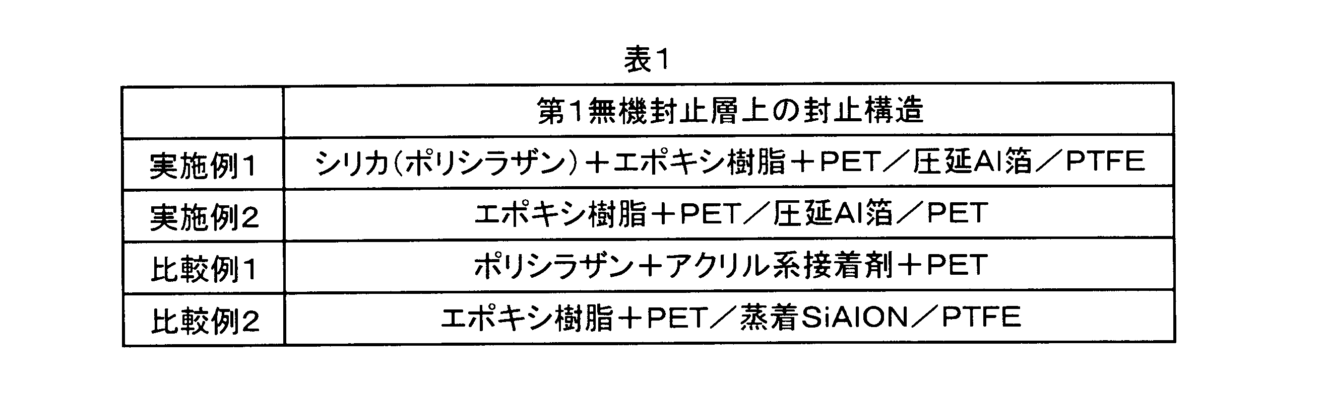
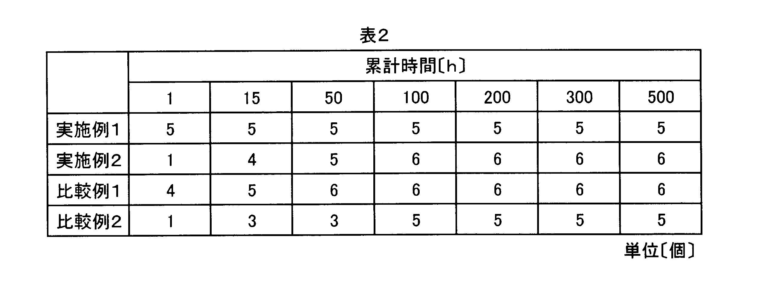


また、表3のように比較例1,2に比べて面内分布が大きく、均熱性が良いため、表4のように輝度分布が小さいという結果につながった。 In the organic EL device of Example 2, as shown in Table 2, the number of dark spots formed at the initial stage of the start of the acceleration test was smaller than that of Comparative Example 1. Further, although dark spots were newly generated as time passed, it was found that the growth rate of dark spots was small as shown in FIG. Specifically, the rate of change (growth rate) of the dark spot after 500 hours with respect to the diameter size of the dark spot after 1 hour was in the range of 1.32 to 1.77.
Further, as shown in Table 3, the in-plane distribution is larger than that of Comparative Examples 1 and 2 and the heat uniformity is good, leading to the result that the luminance distribution is small as shown in Table 4.
2 透明基板(透明絶縁基板)
3 第1電極層(透明酸化物電極層)
5 機能層(有機発光層)
6 第2電極層(金属電極層)
7 無機封止層
8 接着材層
10 有機EL素子
11 金属箔
12,13 絶縁性樹脂膜
15 伝熱封止層
20,22 陽極給電部(導電層,第1電極連通部)
21 陰極給電部(導電層,第2電極連通部)
25 発光素子
30 発光領域
31 給電領域(第1給電領域)
32 給電領域(第2給電領域)
33,35 補助電極領域
34 発光面
40 電極固定部
41,42 補助電極層(導電層)
48 孤立部
50 第1無機封止層
51 第2無機封止層
52 通電領域
60 伝熱封止積層構造 1
3 First electrode layer (transparent oxide electrode layer)
5 Functional layer (organic light-emitting layer)
6 Second electrode layer (metal electrode layer)
7
21 Cathode feeding part (conductive layer, second electrode communication part)
25
32 Power supply area (second power supply area)
33, 35
48
Claims (21)
- 多角形状の透明基板の一方の主面上に、第1電極層と、有機発光層と、第2電極層が積層された有機EL素子を有した有機EL装置であって、
前記透明基板を平面視したときに、駆動時に発光する発光領域を備えた有機EL装置において、
少なくとも発光領域の有機EL素子に、無機封止層と、接着材層と、伝熱封止層が積層されており、
さらに、前記透明基板を平面視したときに、発光領域の外側であって発光領域の外縁の一部又は全部に沿って配される通電領域を有し、
通電領域において、発光領域から延伸した第1電極層と、第1電極層よりも熱伝導率の大きい導電層と、前記無機封止層と、前記接着材層と、前記伝熱封止層がこの順に互いに接触するように積層された伝熱封止積層構造が形成されており、
当該伝熱封止積層構造は、線状又は面状であって、透明基板の各辺のいずれか又は全部の近傍に位置し、対応する各辺に沿って延伸していることを特徴とする有機EL装置。 An organic EL device having an organic EL element in which a first electrode layer, an organic light emitting layer, and a second electrode layer are stacked on one main surface of a polygonal transparent substrate,
In the organic EL device provided with a light emitting region that emits light when driven when the transparent substrate is viewed in plan view,
An inorganic sealing layer, an adhesive layer, and a heat transfer sealing layer are laminated on at least the organic EL element in the light emitting region,
Furthermore, when the transparent substrate is viewed in plan, it has a current-carrying region that is arranged along a part or all of the outer edge of the light-emitting region outside the light-emitting region,
In the energized region, the first electrode layer extended from the light emitting region, the conductive layer having a higher thermal conductivity than the first electrode layer, the inorganic sealing layer, the adhesive layer, and the heat transfer sealing layer A heat transfer sealing laminated structure is formed so as to be in contact with each other in this order,
The heat transfer sealing laminated structure is linear or planar, is located near any or all of the sides of the transparent substrate, and extends along the corresponding sides. Organic EL device. - 前記伝熱封止積層構造の延伸長さは、少なくとも前記対応する各辺の長さの半分以上の長さであることを特徴とする請求項1に記載の有機EL装置。 2. The organic EL device according to claim 1, wherein the stretched length of the heat transfer sealing laminated structure is at least half the length of each corresponding side.
- 前記伝熱封止層は、少なくとも絶縁性樹脂膜と金属箔を有し、
当該絶縁性樹脂膜は、前記接着材層と当該金属箔の間に介在していることを特徴とする請求項1に記載の有機EL装置。 The heat transfer sealing layer has at least an insulating resin film and a metal foil,
The organic EL device according to claim 1, wherein the insulating resin film is interposed between the adhesive layer and the metal foil. - 前記伝熱封止層は、2層の絶縁性樹脂膜と金属箔を有し、
当該金属箔は、前記2層の絶縁性樹脂膜の間に介在していることを特徴とする請求項1乃至3のいずれかに記載の有機EL装置。 The heat transfer sealing layer has two insulating resin films and a metal foil,
The organic EL device according to claim 1, wherein the metal foil is interposed between the two insulating resin films. - 前記絶縁性樹脂膜は、ポリエチレンテレフタレート、ポリ塩化ビニリデン、及びポリテトラフルオロエチレンからなる群より選ばれた少なくとも1種によって形成されていることを特徴とする請求項3又は4に記載の有機EL装置。 5. The organic EL device according to claim 3, wherein the insulating resin film is formed of at least one selected from the group consisting of polyethylene terephthalate, polyvinylidene chloride, and polytetrafluoroethylene. .
- 前記通電領域は、外部電源と電気的に接続可能な給電領域を有し、
前記給電領域は、少なくとも透明基板の一辺側にあって、発光領域の第1電極層と電気的に接続された第1電極連通部と、発光領域の第2電極層と電気的に接続された第2電極連通部が位置していることを特徴とする請求項1乃至5のいずれかに記載の有機EL装置。 The energization region has a power supply region that can be electrically connected to an external power source,
The power supply region is at least on one side of the transparent substrate, and is electrically connected to the first electrode communication portion electrically connected to the first electrode layer of the light emitting region and to the second electrode layer of the light emitting region. 6. The organic EL device according to claim 1, wherein the second electrode communication portion is located. - 前記通電領域は、外部電源と電気的に接続可能な給電領域を有し、
前記給電領域は、少なくとも透明基板の一辺側にあって、発光領域の第1電極層と電気的に接続された2つの第1電極連通部と、発光領域の第2電極層と電気的に接続された第2電極連通部が位置しており、
さらに、前記透明基板の一辺に沿って、第1電極連通部、第2電極連通部、第1電極連通部の順に並列していることを特徴とする請求項1乃至6のいずれかに記載の有機EL装置。 The energization region has a power supply region that can be electrically connected to an external power source,
The power supply region is at least on one side of the transparent substrate, and is electrically connected to two first electrode communication portions electrically connected to the first electrode layer of the light emitting region, and to the second electrode layer of the light emitting region. The second electrode communicating portion is located,
Furthermore, along the one side of the said transparent substrate, it has arranged in parallel in order of the 1st electrode communication part, the 2nd electrode communication part, and the 1st electrode communication part. Organic EL device. - 前記通電領域は、外部電源と電気的に接続可能な給電領域を有し、
前記給電領域は、第1電極層の一部であって発光領域の第1電極層と物理的に分離された島状の孤立部が位置しており、
前記給電領域において、前記孤立部と発光領域から延びた第2電極層が物理的に接続される電極固定部を備えることを特徴とする請求項1乃至7のいずれかに記載の有機EL装置。 The energization region has a power supply region that can be electrically connected to an external power source,
The feeding region is a part of the first electrode layer, and an island-shaped isolated portion physically separated from the first electrode layer of the light emitting region is located,
8. The organic EL device according to claim 1, further comprising: an electrode fixing portion that physically connects the isolated portion and the second electrode layer extending from the light emitting region in the power feeding region. 9. - 前記通電領域は、外部電源と電気的に接続可能な給電領域を有し、
当該給電領域は、透明基板の一辺側に位置する第1給電領域と、透明基板の一辺と対辺側に位置する第2給電領域からなり、
前記第1給電領域は、発光領域の第1電極層と電気的に接続された第1電極連通部と、発光領域の第2電極層と電気的に接続された第2電極連通部が位置しており、
さらに、前記第2給電領域にも、発光領域の第1電極層と電気的に接続された第1電極連通部と、発光領域の第2電極層と電気的に接続された第1電極連通部が位置していることを特徴とする請求項1乃至8のいずれかに記載の有機EL装置。 The energization region has a power supply region that can be electrically connected to an external power source,
The power supply area includes a first power supply area located on one side of the transparent substrate and a second power supply area located on one side and the opposite side of the transparent substrate,
The first power supply region includes a first electrode communication portion electrically connected to the first electrode layer in the light emitting region and a second electrode communication portion electrically connected to the second electrode layer in the light emission region. And
Furthermore, the first electrode communication portion electrically connected to the first electrode layer in the light emitting region and the first electrode communication portion electrically connected to the second electrode layer in the light emitting region are also provided in the second power feeding region. The organic EL device according to claim 1, wherein the organic EL device is located. - 前記通電領域は、第1電極層内の電気伝導を補助する補助電極領域を有し、
前記補助電極領域は、前記第1給電領域と前記第2給電領域を結ぶように延伸しており、
前記伝熱封止積層構造は、補助電極領域の延伸方向に延びていることを特徴とする請求項9に記載の有機EL装置。 The energization region has an auxiliary electrode region that assists electrical conduction in the first electrode layer,
The auxiliary electrode region extends so as to connect the first feeding region and the second feeding region,
The organic EL device according to claim 9, wherein the heat transfer sealing laminated structure extends in the extending direction of the auxiliary electrode region. - 前記通電領域は、外部電源と電気的に接続可能な給電領域と、第1電極層内の電気伝導を補助する補助電極領域から形成されており、
前記給電領域は、透明基板の一辺側に、第1電極層と電気的に接続された第1電極連通部と、第2電極層と電気的に接続された第2電極連通部を有し、
前記補助電極領域は、前記透明基板の一辺に対して直交する方向に延伸し、かつ、前記発光領域及び当該給電領域に隣接するものであり、
発光領域から延びて補助電極領域に位置する第1電極層が、積層体の積層方向で導電層と直接接触することによって伝熱封止積層構造が形成されるものであることを特徴とする請求項1乃至10のいずれかに記載の有機EL装置。 The energization region is formed of a power supply region that can be electrically connected to an external power source, and an auxiliary electrode region that assists electrical conduction in the first electrode layer,
The power supply region has a first electrode communication portion electrically connected to the first electrode layer and a second electrode communication portion electrically connected to the second electrode layer on one side of the transparent substrate,
The auxiliary electrode region extends in a direction perpendicular to one side of the transparent substrate, and is adjacent to the light emitting region and the power feeding region,
The first electrode layer extending from the light emitting region and positioned in the auxiliary electrode region is in direct contact with the conductive layer in the stacking direction of the stacked body to form a heat transfer sealing stacked structure. Item 11. An organic EL device according to any one of Items 1 to 10. - 前記無機封止層は、酸素、炭素、窒素の中から選ばれた1種類以上の元素と、ケイ素元素とからなるシリコン合金により形成される無機合金層を有していることを特徴とする請求項1乃至11のいずれかに記載の有機EL装置。 The inorganic sealing layer has an inorganic alloy layer formed of a silicon alloy composed of one or more elements selected from oxygen, carbon, and nitrogen and a silicon element. Item 12. The organic EL device according to any one of Items 1 to 11.
- 前記無機封止層は、湿式法によって形成されてなる第1無機封止層と、乾式法によって形成されてなる第2無機封止層から形成されていることを特徴とする請求項1乃至12のいずれかに記載の有機EL装置。 13. The inorganic sealing layer is formed of a first inorganic sealing layer formed by a wet method and a second inorganic sealing layer formed by a dry method. The organic EL device according to any one of the above.
- 前記接着材層は、エポキシ樹脂であることを特徴とする請求項1乃至13のいずれかに記載の有機EL装置。 The organic EL device according to any one of claims 1 to 13, wherein the adhesive layer is an epoxy resin.
- 透明基板の他方の主面に駆動時に発光する発光面を有し、
当該発光面の面内輝度分布は、90パーセント以上98パーセント以内に収まっていることを特徴とする請求項1乃至14のいずれかに記載の有機EL装置。 The other main surface of the transparent substrate has a light emitting surface that emits light when driven,
15. The organic EL device according to claim 1, wherein the in-plane luminance distribution of the light emitting surface is within 90% to 98%. - 四角形状の透明絶縁基板の一方の主面上に、透明酸化物電極層と、有機発光層と、金属電極層が積層された有機EL素子を有した有機EL装置であって、
前記透明絶縁基板を平面視したときに、駆動時に発光する発光領域を有する有機EL装置において、
少なくとも発光領域の有機EL素子に、無機封止層と、接着材層と、伝熱封止層が積層されており、
さらに、前記透明絶縁基板を平面視したときに、発光領域の外側であって発光領域の外縁の一部又は全部に沿って配される通電領域を有し、
通電領域において、発光領域から延伸した前記透明酸化物電極層と、前記金属電極層と、前記無機封止層と、前記接着材層と、前記伝熱封止層がこの順に互いに接触するように積層された伝熱封止積層構造が形成されており、
当該伝熱封止積層構造は、線状又は面状であって、透明絶縁基板の各辺のいずれか又は全部の近傍に位置し、対応する各辺に沿って延伸していることを特徴とする有機EL装置。 An organic EL device having an organic EL element in which a transparent oxide electrode layer, an organic light emitting layer, and a metal electrode layer are laminated on one main surface of a rectangular transparent insulating substrate,
In the organic EL device having a light emitting region that emits light when driven when the transparent insulating substrate is viewed in plan view,
An inorganic sealing layer, an adhesive layer, and a heat transfer sealing layer are laminated on at least the organic EL element in the light emitting region,
Furthermore, when the transparent insulating substrate is viewed in plan, it has a current-carrying region that is arranged along a part or all of the outer edge of the light-emitting region outside the light-emitting region,
In the energized region, the transparent oxide electrode layer, the metal electrode layer, the inorganic sealing layer, the adhesive layer, and the heat transfer sealing layer that are extended from the light emitting region are in contact with each other in this order. A laminated heat transfer sealing laminated structure is formed,
The heat transfer sealing laminated structure is linear or planar, is located in the vicinity of any or all of the sides of the transparent insulating substrate, and extends along the corresponding sides. Organic EL device. - 請求項1乃至15のいずれかに記載の有機EL装置の製造方法であって、
透明基板上に有機EL素子を形成する有機EL素子形成工程と、
無機封止層を形成する無機封止層形成工程と、
接着材層によって無機封止層に伝熱封止層を接着する伝熱封止層接着工程を含んでおり、
前記有機EL素子形成工程は、第1電極層より上方の積層体を部分的に除去する第1除去工程と、
当該除去部位上に第2電極層を積層する第2電極積層工程を含んでいることを特徴とする有機EL装置の製造方法。 It is a manufacturing method of the organic EL device according to any one of claims 1 to 15,
An organic EL element forming step of forming an organic EL element on a transparent substrate;
An inorganic sealing layer forming step of forming the inorganic sealing layer;
A heat transfer sealing layer adhesion step of adhering the heat transfer sealing layer to the inorganic sealing layer by the adhesive layer,
The organic EL element formation step includes a first removal step of partially removing the stacked body above the first electrode layer;
A method of manufacturing an organic EL device, comprising a second electrode stacking step of stacking a second electrode layer on the removal site. - 前記導電層は、第2電極層であり、
前記除去部位上に積層した第2電極層は、伝熱封止積層構造の一部を形成することを特徴とする請求項17に記載の有機EL装置の製造方法。 The conductive layer is a second electrode layer;
18. The method of manufacturing an organic EL device according to claim 17, wherein the second electrode layer laminated on the removal site forms a part of a heat transfer sealing laminated structure. - 前記有機EL素子形成工程は、発光領域の第1電極層と物理的に分離された孤立部を形成する孤立部形成工程と、
少なくとも孤立部上に有機発光層を積層する有機発光層積層工程と、
有機発光層を部分的に除去する有機発光層除去工程と、
当該除去部位上に第2電極層を積層する第2電極積層工程を含んでいることを特徴とする請求項17又は18に記載の有機EL装置の製造方法。 The organic EL element forming step includes an isolated portion forming step of forming an isolated portion physically separated from the first electrode layer of the light emitting region,
An organic light emitting layer laminating step of laminating an organic light emitting layer on at least the isolated portion;
An organic light emitting layer removing step of partially removing the organic light emitting layer;
19. The method of manufacturing an organic EL device according to claim 17 or 18, further comprising a second electrode stacking step of stacking a second electrode layer on the removal site. - 請求項12又は13に記載の有機EL装置の製造方法であって、
透明基板上に有機EL素子を形成する有機EL素子形成工程と、
無機封止層を形成する無機封止層形成工程と、
接着材層によって無機封止層に伝熱封止層を接着する伝熱封止層接着工程を含んでおり、
前記無機封止層形成工程は、CVD法によって第1無機封止層を形成する工程と、シリカ転化によって第2無機封止層を形成する工程を有することを特徴とする有機EL装置の製造方法。 It is a manufacturing method of the organic EL device according to claim 12 or 13,
An organic EL element forming step of forming an organic EL element on a transparent substrate;
An inorganic sealing layer forming step of forming the inorganic sealing layer;
A heat transfer sealing layer adhesion step of adhering the heat transfer sealing layer to the inorganic sealing layer by the adhesive layer,
The inorganic sealing layer forming step includes a step of forming a first inorganic sealing layer by a CVD method and a step of forming a second inorganic sealing layer by silica conversion. . - 前記第2無機封止層は、ポリシラザンを原料とすることを特徴とする請求項20に記載の有機EL装置の製造方法。 21. The method of manufacturing an organic EL device according to claim 20, wherein the second inorganic sealing layer is made of polysilazane as a raw material.
Priority Applications (3)
| Application Number | Priority Date | Filing Date | Title |
|---|---|---|---|
| US14/399,896 US9508959B2 (en) | 2012-05-10 | 2013-04-26 | Organic EL device and method for manufacturing same |
| JP2014514690A JP6163483B2 (en) | 2012-05-10 | 2013-04-26 | Organic EL device and manufacturing method thereof |
| EP13787451.7A EP2849534A4 (en) | 2012-05-10 | 2013-04-26 | Organic el device and method for manufacturing same |
Applications Claiming Priority (4)
| Application Number | Priority Date | Filing Date | Title |
|---|---|---|---|
| JP2012-108106 | 2012-05-10 | ||
| JP2012108106 | 2012-05-10 | ||
| JP2012135238 | 2012-06-14 | ||
| JP2012-135238 | 2012-06-14 |
Publications (1)
| Publication Number | Publication Date |
|---|---|
| WO2013168619A1 true WO2013168619A1 (en) | 2013-11-14 |
Family
ID=49550664
Family Applications (1)
| Application Number | Title | Priority Date | Filing Date |
|---|---|---|---|
| PCT/JP2013/062453 WO2013168619A1 (en) | 2012-05-10 | 2013-04-26 | Organic el device and method for manufacturing same |
Country Status (4)
| Country | Link |
|---|---|
| US (1) | US9508959B2 (en) |
| EP (1) | EP2849534A4 (en) |
| JP (1) | JP6163483B2 (en) |
| WO (1) | WO2013168619A1 (en) |
Cited By (6)
| Publication number | Priority date | Publication date | Assignee | Title |
|---|---|---|---|---|
| WO2015129892A1 (en) * | 2014-02-28 | 2015-09-03 | コニカミノルタ株式会社 | Organic electroluminescent element manufacturing method and manufacturing device |
| EP2995850A1 (en) * | 2014-09-15 | 2016-03-16 | Valeo Vision | Multifunctional light module with segmented oled diode |
| WO2016139209A1 (en) * | 2015-03-03 | 2016-09-09 | Osram Oled Gmbh | Optoelectronic component and a method for producing an optoelectronic component |
| CN107112436A (en) * | 2015-01-13 | 2017-08-29 | 欧司朗Oled股份有限公司 | Organic luminescent device |
| EP3109918A4 (en) * | 2014-02-18 | 2017-10-25 | LG Chem, Ltd. | Encapsulation film, and organic electronic device comprising same |
| WO2020184329A1 (en) * | 2019-03-12 | 2020-09-17 | ソニーセミコンダクタソリューションズ株式会社 | Display device and electronic instrument |
Families Citing this family (7)
| Publication number | Priority date | Publication date | Assignee | Title |
|---|---|---|---|---|
| DE102012200485A1 (en) * | 2012-01-13 | 2013-07-18 | Osram Opto Semiconductors Gmbh | Organic light-emitting device and method for processing an organic light-emitting device |
| CN105470409A (en) | 2016-01-04 | 2016-04-06 | 京东方科技集团股份有限公司 | Organic light-emitting diode (OLED) package structure, fabrication method thereof and display device |
| JP6654913B2 (en) | 2016-01-26 | 2020-02-26 | 住友化学株式会社 | Method for manufacturing organic EL element and organic EL element |
| KR20180077939A (en) * | 2016-12-29 | 2018-07-09 | 엘지디스플레이 주식회사 | Lighting apparatus using organic light emitting device and method of fabricating thereof |
| KR102581656B1 (en) * | 2016-12-29 | 2023-09-21 | 엘지디스플레이 주식회사 | Lighting apparatus using organic light emitting device and method of fabricating thereof |
| CN206774584U (en) * | 2017-06-06 | 2017-12-19 | 京东方科技集团股份有限公司 | Thin-film packing structure and display device |
| CN109638053B (en) | 2018-12-15 | 2021-05-07 | 武汉华星光电半导体显示技术有限公司 | Heat radiation structure of flexible display |
Citations (6)
| Publication number | Priority date | Publication date | Assignee | Title |
|---|---|---|---|---|
| JP2002093573A (en) * | 2000-09-14 | 2002-03-29 | Nisshin Steel Co Ltd | Insulating sealing component for organic el device |
| JP2007080569A (en) * | 2005-09-12 | 2007-03-29 | Toyota Industries Corp | Method for manufacturing organic electroluminescence element |
| JP2010198980A (en) * | 2009-02-26 | 2010-09-09 | Panasonic Electric Works Co Ltd | Planar light-emitting device |
| JP2010231977A (en) * | 2009-03-26 | 2010-10-14 | Panasonic Electric Works Co Ltd | Thin sealed organic el element |
| JP2010245026A (en) | 2009-03-16 | 2010-10-28 | Konica Minolta Holdings Inc | Organic electronics panel |
| JP2011096374A (en) * | 2009-10-27 | 2011-05-12 | Rohm Co Ltd | Organic el device |
Family Cites Families (6)
| Publication number | Priority date | Publication date | Assignee | Title |
|---|---|---|---|---|
| US8486487B2 (en) * | 2005-02-17 | 2013-07-16 | Konica Minolta Holdings, Inc. | Gas barrier film, gas barrier film manufacturing method, resin substrate for organic electroluminescent device using the aforesaid gas barrier film, and organic electroluminescent device using the aforementioned gas barrier film |
| JP4830411B2 (en) * | 2005-09-07 | 2011-12-07 | 株式会社豊田自動織機 | Manufacturing method of organic EL device |
| US20070222908A1 (en) * | 2006-02-07 | 2007-09-27 | Joo-Han Kim | Thin film transistor substrate, display panel having the same and method of manufacturing the same |
| KR100811473B1 (en) * | 2006-10-17 | 2008-03-07 | 엘지전자 주식회사 | Light emitting panel and light source comprising the same |
| KR20130069602A (en) * | 2010-04-27 | 2013-06-26 | 루미오텍 가부시키가이샤 | Organic el illumination device |
| KR20130004829A (en) * | 2011-07-04 | 2013-01-14 | 삼성디스플레이 주식회사 | Organic light emitting diode lighting apparatus |
-
2013
- 2013-04-26 US US14/399,896 patent/US9508959B2/en active Active
- 2013-04-26 EP EP13787451.7A patent/EP2849534A4/en not_active Withdrawn
- 2013-04-26 JP JP2014514690A patent/JP6163483B2/en active Active
- 2013-04-26 WO PCT/JP2013/062453 patent/WO2013168619A1/en active Application Filing
Patent Citations (6)
| Publication number | Priority date | Publication date | Assignee | Title |
|---|---|---|---|---|
| JP2002093573A (en) * | 2000-09-14 | 2002-03-29 | Nisshin Steel Co Ltd | Insulating sealing component for organic el device |
| JP2007080569A (en) * | 2005-09-12 | 2007-03-29 | Toyota Industries Corp | Method for manufacturing organic electroluminescence element |
| JP2010198980A (en) * | 2009-02-26 | 2010-09-09 | Panasonic Electric Works Co Ltd | Planar light-emitting device |
| JP2010245026A (en) | 2009-03-16 | 2010-10-28 | Konica Minolta Holdings Inc | Organic electronics panel |
| JP2010231977A (en) * | 2009-03-26 | 2010-10-14 | Panasonic Electric Works Co Ltd | Thin sealed organic el element |
| JP2011096374A (en) * | 2009-10-27 | 2011-05-12 | Rohm Co Ltd | Organic el device |
Non-Patent Citations (1)
| Title |
|---|
| See also references of EP2849534A4 |
Cited By (10)
| Publication number | Priority date | Publication date | Assignee | Title |
|---|---|---|---|---|
| EP3109918A4 (en) * | 2014-02-18 | 2017-10-25 | LG Chem, Ltd. | Encapsulation film, and organic electronic device comprising same |
| US10096797B2 (en) | 2014-02-18 | 2018-10-09 | Lg Chem, Ltd. | Encapsulation film and organic electronic device comprising the same |
| US10181577B1 (en) | 2014-02-18 | 2019-01-15 | Lg Chem, Ltd. | Encapsulation film and organic electronic device comprising the same |
| WO2015129892A1 (en) * | 2014-02-28 | 2015-09-03 | コニカミノルタ株式会社 | Organic electroluminescent element manufacturing method and manufacturing device |
| EP2995850A1 (en) * | 2014-09-15 | 2016-03-16 | Valeo Vision | Multifunctional light module with segmented oled diode |
| FR3025942A1 (en) * | 2014-09-15 | 2016-03-18 | Valeo Vision | MULTIFUNCTION LUMINOUS MODULE WITH SEGMENTED OLED DIODE |
| US9936562B2 (en) | 2014-09-15 | 2018-04-03 | Valeo Vision | Multifunction luminous module with segmented OLED diode |
| CN107112436A (en) * | 2015-01-13 | 2017-08-29 | 欧司朗Oled股份有限公司 | Organic luminescent device |
| WO2016139209A1 (en) * | 2015-03-03 | 2016-09-09 | Osram Oled Gmbh | Optoelectronic component and a method for producing an optoelectronic component |
| WO2020184329A1 (en) * | 2019-03-12 | 2020-09-17 | ソニーセミコンダクタソリューションズ株式会社 | Display device and electronic instrument |
Also Published As
| Publication number | Publication date |
|---|---|
| US9508959B2 (en) | 2016-11-29 |
| JP6163483B2 (en) | 2017-07-12 |
| JPWO2013168619A1 (en) | 2016-01-07 |
| EP2849534A4 (en) | 2016-02-10 |
| US20150123095A1 (en) | 2015-05-07 |
| EP2849534A1 (en) | 2015-03-18 |
Similar Documents
| Publication | Publication Date | Title |
|---|---|---|
| JP6163483B2 (en) | Organic EL device and manufacturing method thereof | |
| JP5106413B2 (en) | Organic LED element | |
| US9054334B2 (en) | Organic EL device | |
| TW200915909A (en) | Substrate with barrier layer, display device and manufacturing method thereof | |
| US9608229B2 (en) | Organic EL lighting panel substrate, organic EL lighting panel, and organic EL lighting device | |
| US9373815B2 (en) | Sealing layer of organic EL device | |
| EP3349267B1 (en) | Lighting apparatus using organic light emitting device and method of fabricating thereof | |
| JP2015111505A (en) | Organic electroluminescent device | |
| WO2012114615A1 (en) | Organic el device | |
| KR20160024395A (en) | Method for processing an electronic component and electronic component arrangement | |
| US20130334958A1 (en) | Planar light emitting device and manufacturing method thereof | |
| JP6124622B2 (en) | Organic EL device | |
| JP6106466B2 (en) | Organic EL device and manufacturing method thereof | |
| US8704443B2 (en) | Organic EL device | |
| JP2012212555A (en) | Light-emitting device | |
| WO2012114618A1 (en) | Organic el device | |
| JP6091233B2 (en) | Organic EL device | |
| JP5842088B2 (en) | Organic EL device and method for manufacturing organic EL device | |
| WO2012120746A1 (en) | Organic el device | |
| JP6192912B2 (en) | Organic EL device | |
| JP6124623B2 (en) | Organic EL device | |
| JP6150492B2 (en) | Organic EL device | |
| JP2017204488A (en) | Organic EL device | |
| WO2012132823A1 (en) | Light-emitting device | |
| JP2014059978A (en) | Organic el device |
Legal Events
| Date | Code | Title | Description |
|---|---|---|---|
| 121 | Ep: the epo has been informed by wipo that ep was designated in this application |
Ref document number: 13787451 Country of ref document: EP Kind code of ref document: A1 |
|
| ENP | Entry into the national phase |
Ref document number: 2014514690 Country of ref document: JP Kind code of ref document: A |
|
| WWE | Wipo information: entry into national phase |
Ref document number: 14399896 Country of ref document: US |
|
| NENP | Non-entry into the national phase |
Ref country code: DE |
|
| WWE | Wipo information: entry into national phase |
Ref document number: 2013787451 Country of ref document: EP |