WO2013164971A1 - X線検査方法及びx線検査装置 - Google Patents
X線検査方法及びx線検査装置 Download PDFInfo
- Publication number
- WO2013164971A1 WO2013164971A1 PCT/JP2013/062127 JP2013062127W WO2013164971A1 WO 2013164971 A1 WO2013164971 A1 WO 2013164971A1 JP 2013062127 W JP2013062127 W JP 2013062127W WO 2013164971 A1 WO2013164971 A1 WO 2013164971A1
- Authority
- WO
- WIPO (PCT)
- Prior art keywords
- image
- ray
- shape
- simulation
- inspection
- Prior art date
Links
Images


Classifications
-
- G—PHYSICS
- G01—MEASURING; TESTING
- G01N—INVESTIGATING OR ANALYSING MATERIALS BY DETERMINING THEIR CHEMICAL OR PHYSICAL PROPERTIES
- G01N23/00—Investigating or analysing materials by the use of wave or particle radiation, e.g. X-rays or neutrons, not covered by groups G01N3/00 – G01N17/00, G01N21/00 or G01N22/00
- G01N23/02—Investigating or analysing materials by the use of wave or particle radiation, e.g. X-rays or neutrons, not covered by groups G01N3/00 – G01N17/00, G01N21/00 or G01N22/00 by transmitting the radiation through the material
- G01N23/04—Investigating or analysing materials by the use of wave or particle radiation, e.g. X-rays or neutrons, not covered by groups G01N3/00 – G01N17/00, G01N21/00 or G01N22/00 by transmitting the radiation through the material and forming images of the material
-
- G—PHYSICS
- G01—MEASURING; TESTING
- G01B—MEASURING LENGTH, THICKNESS OR SIMILAR LINEAR DIMENSIONS; MEASURING ANGLES; MEASURING AREAS; MEASURING IRREGULARITIES OF SURFACES OR CONTOURS
- G01B15/00—Measuring arrangements characterised by the use of electromagnetic waves or particle radiation, e.g. by the use of microwaves, X-rays, gamma rays or electrons
- G01B15/04—Measuring arrangements characterised by the use of electromagnetic waves or particle radiation, e.g. by the use of microwaves, X-rays, gamma rays or electrons for measuring contours or curvatures
-
- G—PHYSICS
- G06—COMPUTING; CALCULATING OR COUNTING
- G06T—IMAGE DATA PROCESSING OR GENERATION, IN GENERAL
- G06T7/00—Image analysis
- G06T7/0002—Inspection of images, e.g. flaw detection
- G06T7/0004—Industrial image inspection
- G06T7/0006—Industrial image inspection using a design-rule based approach
-
- G—PHYSICS
- G06—COMPUTING; CALCULATING OR COUNTING
- G06T—IMAGE DATA PROCESSING OR GENERATION, IN GENERAL
- G06T7/00—Image analysis
- G06T7/0002—Inspection of images, e.g. flaw detection
- G06T7/0004—Industrial image inspection
- G06T7/001—Industrial image inspection using an image reference approach
-
- H—ELECTRICITY
- H01—ELECTRIC ELEMENTS
- H01L—SEMICONDUCTOR DEVICES NOT COVERED BY CLASS H10
- H01L22/00—Testing or measuring during manufacture or treatment; Reliability measurements, i.e. testing of parts without further processing to modify the parts as such; Structural arrangements therefor
- H01L22/10—Measuring as part of the manufacturing process
- H01L22/12—Measuring as part of the manufacturing process for structural parameters, e.g. thickness, line width, refractive index, temperature, warp, bond strength, defects, optical inspection, electrical measurement of structural dimensions, metallurgic measurement of diffusions
-
- G—PHYSICS
- G01—MEASURING; TESTING
- G01N—INVESTIGATING OR ANALYSING MATERIALS BY DETERMINING THEIR CHEMICAL OR PHYSICAL PROPERTIES
- G01N2223/00—Investigating materials by wave or particle radiation
- G01N2223/40—Imaging
- G01N2223/418—Imaging electron microscope
-
- G—PHYSICS
- G01—MEASURING; TESTING
- G01N—INVESTIGATING OR ANALYSING MATERIALS BY DETERMINING THEIR CHEMICAL OR PHYSICAL PROPERTIES
- G01N2223/00—Investigating materials by wave or particle radiation
- G01N2223/60—Specific applications or type of materials
- G01N2223/611—Specific applications or type of materials patterned objects; electronic devices
- G01N2223/6113—Specific applications or type of materials patterned objects; electronic devices printed circuit board [PCB]
-
- G—PHYSICS
- G06—COMPUTING; CALCULATING OR COUNTING
- G06T—IMAGE DATA PROCESSING OR GENERATION, IN GENERAL
- G06T2207/00—Indexing scheme for image analysis or image enhancement
- G06T2207/10—Image acquisition modality
- G06T2207/10072—Tomographic images
- G06T2207/10081—Computed x-ray tomography [CT]
-
- G—PHYSICS
- G06—COMPUTING; CALCULATING OR COUNTING
- G06T—IMAGE DATA PROCESSING OR GENERATION, IN GENERAL
- G06T2207/00—Indexing scheme for image analysis or image enhancement
- G06T2207/10—Image acquisition modality
- G06T2207/10116—X-ray image
-
- G—PHYSICS
- G06—COMPUTING; CALCULATING OR COUNTING
- G06T—IMAGE DATA PROCESSING OR GENERATION, IN GENERAL
- G06T2207/00—Indexing scheme for image analysis or image enhancement
- G06T2207/20—Special algorithmic details
- G06T2207/20024—Filtering details
-
- G—PHYSICS
- G06—COMPUTING; CALCULATING OR COUNTING
- G06T—IMAGE DATA PROCESSING OR GENERATION, IN GENERAL
- G06T2207/00—Indexing scheme for image analysis or image enhancement
- G06T2207/30—Subject of image; Context of image processing
- G06T2207/30108—Industrial image inspection
- G06T2207/30148—Semiconductor; IC; Wafer
Definitions
- the present invention relates to an X-ray inspection method and an X-ray inspection apparatus for measuring the shape of an inspection object based on an X-ray image.
- a semiconductor inspection method for quickly and accurately counting semiconductor cells using a scanning electron microscope (SEM) is known (see, for example, Patent Document 1). Also known is a method for measuring and inspecting the shape of an inspection object such as a through-silicon via (hereinafter referred to as “TSV”) formed on a silicon wafer using an SEM or an X-ray CT apparatus. Yes.
- SEM scanning electron microscope
- the present invention has been made in view of the above, and an object of the present invention is to provide an X-ray inspection method and an X-ray inspection apparatus that can perform non-destructive measurement of the shape of an inspection object at high speed.
- a simulation image generation step of generating a plurality of simulation images having different shape parameters of the inspection target an X-ray imaging step of capturing the X-ray image of the inspection target,
- an X-ray inspection method and an X-ray inspection apparatus that can perform non-destructive measurement of the shape of an inspection object at high speed.
- FIG. 1 is a diagram illustrating a schematic configuration of an X-ray inspection apparatus 100 according to the present embodiment.
- an X-ray inspection apparatus 100 includes an image processing apparatus 101 and an X-ray imaging apparatus 120.
- the X-ray imaging apparatus 120 captures an X-ray image to be inspected, and Based on the X-ray image, the image processing apparatus 101 estimates the shape of the inspection object by estimation.
- the image processing apparatus 101 includes an imaging control unit 102, an image generation unit 103, an image processing unit 104, an image database 105, an image matching unit 106, and the like.
- the imaging control unit 102 controls the entire operation including the X-ray source 125, the stage 126, the X-ray camera 127, and the like of the X-ray imaging apparatus 120 that captures an X-ray image to be inspected, and the X-ray imaging apparatus 120 performs imaging. An X-ray image to be inspected is acquired.
- the image generation unit 103 is an example of a simulation image generation unit, and generates X-ray images with different shapes of TSVs of silicon wafers to be inspected by simulation.
- the image generation unit 103 generates a plurality of simulation images based on shape parameters representing the shape of the TSV. A method for generating a simulation image will be described later.
- the image processing unit 104 performs image processing such as distortion correction, contrast correction, and resolution correction on the simulation image generated by the image generation unit 103 and the X-ray image captured by the X-ray imaging apparatus 120.
- the image database 105 is generated by the image generation unit 103, and a plurality of simulation images subjected to image processing by the image processing unit 104 are registered as a library.
- the image matching unit 106 is an example of a shape estimation unit, and performs a matching process between an X-ray image captured by the X-ray imaging apparatus 120 and a simulation image registered in the image database 105, thereby generating a TSV shape. Is estimated. A TSV shape estimation method by matching processing will be described later.
- the X-ray imaging apparatus 120 is an example of an X-ray imaging unit, and includes a fork 121, a notch aligner 122, an optical microscope 123, a thickness measuring device 124, an X-ray source 125, a stage 126, an X-ray camera 127, and the like. It is connected to the processing device 101.
- the X direction shown in the figure is the left-right direction in the drawing parallel to the surface of the stage 126
- the Y direction is parallel to the surface of the stage 126 and perpendicular to the X direction
- the Z direction is perpendicular to the surface of the stage 126.
- the fork 121 holds a silicon wafer having a TSV, and the notch aligner 122 adjusts the notch position.
- the optical microscope 123 can observe the appearance of a silicon wafer placed on the stage 126.
- the thickness measuring device 124 is a spectral interference type thickness measuring device, for example, and can measure the thickness of the silicon wafer.
- the X-ray source 125 irradiates a silicon wafer placed on the stage 126 with X-rays, and an X-ray camera 127 provided on the opposite side of the X-ray source 125 with the stage 126 interposed therebetween, An X-ray image of a silicon wafer is acquired.
- the X-ray camera 127 is configured to include, for example, an image intensifier, a CCD image sensor, and the like.
- the image intensifier converts X-rays that have passed through the inspection target into visible light, and visible light that is incident on the CCD image sensor. Is converted into an electrical signal.
- the output of the X-ray camera 127 is input to the imaging control unit 102 of the image processing apparatus 101 and acquired as an X-ray image to be inspected.
- the X-ray camera 127 is provided so as to be movable in the X and Y directions in the figure, and by moving in the X and Y directions, an X-ray image to be inspected placed on the stage 126 is set in a predetermined direction with respect to the Z direction, for example. It can be taken as a tilted image inclined at an angle ⁇ .
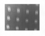
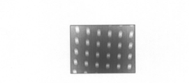
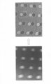
- FIG. 2 illustrates an X-ray image captured by the X-ray imaging apparatus 120 according to the present embodiment.
- FIG. 2 is an X-ray image taken from a direction inclined 15 degrees with respect to the Z direction by the X-ray camera 127.
- the entire shape of the TSV formed on the silicon wafer is determined in this way.
- the shape estimation of TSV is performed using the tilted image of the X-ray image that can be generated.
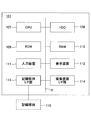
- FIG. 3 is a diagram illustrating a hardware configuration of the image processing apparatus 101 according to the embodiment.
- the image processing apparatus 101 includes a CPU 107, an HDD (Hard Disk Drive) 108, a ROM (Read Only Memory) 109, a RAM (Read and Memory) 110, an input device 111, a display device 112, and a recording medium I. / F unit 113, imaging device I / F unit 114, and the like, which are connected to each other via a bus B.
- a CPU 107 an HDD (Hard Disk Drive) 108, a ROM (Read Only Memory) 109, a RAM (Read and Memory) 110, an input device 111, a display device 112, and a recording medium I. / F unit 113, imaging device I / F unit 114, and the like, which are connected to each other via a bus B.
- an HDD Hard Disk Drive
- ROM Read Only Memory
- RAM Read and Memory
- the CPU 107 is an arithmetic device that implements control of the X-ray imaging apparatus 120 and functions of the image processing apparatus 101 by reading a program and data from a storage device such as the HDD 108 and the ROM 109 onto the RAM 110 and executing processing. is there.
- the CPU 107 functions as the imaging control unit 102, the image generation unit 103, the image processing unit 104, the image matching unit 106, and the like.
- the HDD 108 is a non-volatile storage device that stores programs and data.
- the stored programs and data include an OS (Operating System) that is basic software for controlling the entire image processing apparatus 101, and application software that provides various functions on the OS.
- the HDD 108 functions as an image database 105 in which a plurality of simulation images generated by the image generation unit 103 are registered.
- the ROM 109 is a nonvolatile semiconductor memory (storage device) that can retain programs and data even when the power is turned off.
- the ROM 109 stores programs and data such as BIOS (Basic Input / Output System), OS settings, and network settings that are executed when the image processing apparatus 101 is activated.
- BIOS Basic Input / Output System
- OS Operating System
- network settings that are executed when the image processing apparatus 101 is activated.
- the RAM 110 is a volatile semiconductor memory (storage device) that temporarily stores programs and data.
- the input device 111 includes, for example, a keyboard and a mouse, and is used to input each operation signal to the image processing device 101.
- the display device 112 includes, for example, a display, and displays an X-ray image to be inspected, a simulation image, a shape measurement result, and the like imaged by the X-ray imaging device 120.
- the recording medium I / F unit 113 is an interface with the recording medium.
- the image processing apparatus 101 can read and / or write the recording medium 115 via the recording medium I / F 113.
- the recording medium 115 includes a flexible disk, CD, DVD (Digital Versatile Disk), SD memory card (SD Memory card), USB memory (Universal Serial Bus memory).
- the imaging device I / F unit 114 is an interface connected to the X-ray imaging device 120.
- the image processing apparatus 101 can perform data communication with the X-ray imaging apparatus 120 via the imaging apparatus I / F unit 114.
- the image processing apparatus 101 may be provided with a communication I / F or the like as an interface for connecting to a network so as to perform data communication with other devices.
- the image generation unit 103 of the image processing apparatus 101 generates a plurality of simulation images corresponding to the X-ray images captured by the X-ray imaging apparatus 120 based on the shape parameter of the TSV to be inspected.
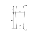
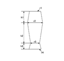
- 4A and 4B are diagrams illustrating the shape parameters of the TSV in the present embodiment.
- the shape parameters of the TSV in this embodiment are as follows: the opening radius r1, the hole middle maximum radius r2, the bottom radius r3, the radius r4 of the portion hemispherically etched at the bottom, up to the maximum radius portion
- the depth h1 is the depth h2 from the maximum radius to the bottom.
- the types and number of parameters used for generating the simulation image are not limited to the above example.
- the parameters may be set corresponding to the shape of the TSV as shown in FIG. It can be set as appropriate according to the configuration of the X-ray imaging apparatus 120 and the like.
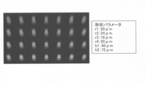
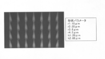
- FIG. 5A and FIG. 5B are diagrams illustrating simulation images generated based on different shape parameters.
- the image generation unit 103 can generate a simulation image corresponding to an X-ray image captured by the X-ray imaging apparatus 120 based on different shape parameters.
- FIG. 6 is a diagram for explaining a simulation image generation method according to this embodiment.
- the image generation unit 103 When generating a simulation image, the image generation unit 103 first generates an aggregate of voxels 51 having different X-ray transmittances according to input shape parameters. Next, when the aggregate of voxels 51 is irradiated with X-rays from an X-ray source 50 defined as a point light source, the amount of X-ray transmission is calculated based on the transmittance of each voxel 51, and the detector 52 A simulation image is generated by reproducing the amount reached as an image.
- the voxels 51 As shown in FIG. 6, for example, materials such as Air, Cu, and Si are defined as the voxels 51, and the voxels 51 are transmitted through the voxels 51 using the transmittances measured individually for the respective materials to the detector 52. Calculate the X-ray dose reached.
- the voxel 51 is a cube of 0.1 ⁇ m, for example, and a simulation image can be generated by setting the transmittance of each voxel 51 to, for example, Air: 1, Cu: 0.981 / 1 ⁇ m, Si: 0.999 / 1 ⁇ m. .
- the values such as the type, size, and transmittance of the voxel are not limited to these, and can be set as appropriate.
- the image generation unit 103 calculates the amount of X-ray transmission through the lower surface of each voxel 51 in order from the side closer to the X-ray source 50 in the above setting, and obtains the X-ray dose reaching the detector 52. As shown in FIG. 5A and FIG. 5B, a simulation image corresponding to the shape parameter is generated.
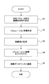
- FIG. 7 shows an example of a flowchart of simulation image generation processing by the image generation unit 103 according to the present embodiment.
- step S1 the shape parameters r1, r2, r3, r4, h1, h2, and the tilt angle for imaging the inspection object (position of the X-ray camera 127) with the TSV design value as the center.
- a plurality of simulation image generation conditions such as the above are set.
- image generation conditions are set at intervals of 0.1 ⁇ m from 19 ⁇ m to 21 ⁇ m with a design value of 20 ⁇ m as the center, and a large number of image generation conditions with different shape parameters are set.
- step S2 the image generation unit 103 generates a plurality of simulation images by the above-described method based on the set plurality of image generation conditions.
- step S3 in order for the image processing unit 104 to match the generated simulation image with the X-ray image captured by the X-ray imaging apparatus 120, image correction processing such as distortion correction described later is performed.
- step S4 a plurality of generated simulation images, a shape parameter, an inclination angle for imaging the inspection object, and the like are made into a library, and in step S5, the data made into the library is registered in the image database 105 for simulation.
- the image generation process ends.
- the image generation unit 103 of the image processing apparatus 101 generates in advance a large number of simulation images having different shape parameters and registers them in the image database 105 by the above-described processing.
- Image distortion correction for the simulation image performed by the image processing unit 104 will be described.
- the X-ray image captured by the X-ray imaging apparatus 120 of the X-ray inspection apparatus 100 may have distortion in the peripheral part due to, for example, an image intensifier provided in the X-ray camera 127. Therefore, the image processing unit 104 performs image distortion correction in order to match the simulation image generated in advance with the X-ray image captured by the X-ray imaging apparatus 120.
- FIG. 8 is a diagram illustrating a flowchart of image distortion correction processing by the image processing unit 104 in the present embodiment.
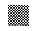
- step S11 an X-ray image of a checkerboard pattern (Checker Board Pattern, hereinafter referred to as “CBP”) captured by the X-ray imaging apparatus 120 is acquired.
- CBP Checker Board Pattern
- the CBP is a sample formed by arranging materials having different amounts of X-ray transmission in a predetermined pattern.
- step S12 XY coordinates of intersections of materials having different X-ray transmission amounts are extracted from the CBP X-ray image.
- step S13 for example, an approximate expression of a quadratic polynomial is obtained from the extracted XY coordinates of the intersection, and in step S14, based on the obtained quadratic polynomial, the actual intersection coordinates of the CBP and X Data for converting the image distortion amount is generated from the difference from the coordinates of the intersection in the line image.
- step S15 based on the generated image distortion amount conversion data, image distortion correction is performed on the simulation image generated by the image generation unit 103, and the process ends.
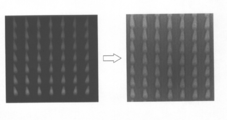
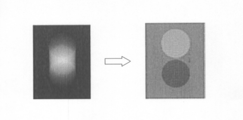
- FIG. 10 is a diagram illustrating image distortion correction of a simulation image in the embodiment.
- the image shown on the left in FIG. 10 is a simulation image generated by the image generation unit 103, and the image shown on the right in FIG. 10 is an example of a simulation image subjected to image distortion correction.
- the matching process with the X-ray image captured by the X-ray imaging apparatus 120 is performed, so that the shape of the TSV to be inspected can be obtained with high accuracy. It becomes possible to estimate.
- the CBP for obtaining the amount of distortion of the X-ray image by the X-ray imaging apparatus 120 is not limited to the example shown in FIG. 9 as long as the amount of distortion of the X-ray image can be grasped.
- image distortion correction is performed on the simulation image generated by the image generation unit 103.
- image distortion correction is performed on the X-ray image captured by the X-ray imaging apparatus 120. May be.
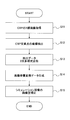
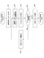
- FIG. 11 is a diagram illustrating a flowchart of the shape estimation process of the inspection target in the present embodiment.
- step S21 the X-ray imaging apparatus 120 captures an X-ray image of a TSV formed on a silicon wafer.
- step S22 the image processing unit 104 of the image processing apparatus 101 performs image correction such as contrast correction and image distortion correction on the captured X-ray image.
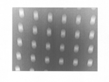
- the image processing unit 104 generates a super-resolution image by performing super-resolution processing on the X-ray image in step S23, and generates a reduced image of the super-resolution image in step S24.
- FIG. 12 illustrates a super-resolution image generated from an X-ray image by the X-ray imaging apparatus 120
- FIG. 13 illustrates a reduced image of the super-resolution image.
- an image of 3770 ⁇ 2830 pixels is created from the X-ray image as the super-resolution image, and an image of 377 ⁇ 283 pixels, which is 1/10 of the super-resolution image, is created as the reduced image.
- the image generation unit 103 described above generates a simulation image having a resolution corresponding to the super-resolution image and the reduced image.
- step S ⁇ b> 25 the image matching unit 106 of the image processing apparatus 101 performs matching between the generated reduced image and the simulation image registered in the image database 105, thereby estimating the TSV shape parameter. I do.
- FIG. 14 shows an example of a flowchart of matching processing in the present embodiment.
- step S31 initial shape parameters for estimating TSV shape parameters are input.
- an initial shape parameter when matching processing is performed using a reduced image for example, a design value of TSV can be used.
- step S32 a simulation image of the shape parameter input from the image database 105 is acquired.
- step S33 a matching score is calculated as an evaluation value representing the similarity between the reduced image of the X-ray image and the simulation image.
- normalized correlation is used in the present embodiment, but geometric correlation, orientation code inquiry (OCM: Orientation Code Matching), etc. may be used, for example.
- step S34 the calculated matching score is compared with a reference value (for example, 0.95). If the matching score is less than or equal to the reference value, the shape parameter is optimized in step S35, and the simulation image of the shape parameter optimized in step S32 is obtained again from the image database 105, and then in step S33. A matching score is calculated.
- a reference value for example 0.95
- FIG. 15 shows an example of a matching score calculation result.
- the matching score is calculated using the simulation image of the input shape parameter.
- the matching score is calculated again using the simulation image having a different shape parameter. Do.
- step S35 the process from step S32 to step S35 is repeated until the value of the matching score exceeds the reference value, and the shape parameter is optimized.
- an optimization algorithm such as a genetic algorithm or a gradient method can be used.
- step S34 If the matching score exceeds the reference value in step S34, the shape parameter is acquired in step S36, and the process ends.
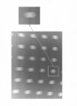
- step S26 the coordinate data of the TSV having the highest matching score is extracted from the reduced image matching score calculation result, and the coordinates extracted from the super-resolution image are extracted. Cut out the image corresponding to the data.
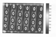
- FIG. 16 is a diagram illustrating a matching score calculation result between the reduced image of the X-ray image and the simulation image.
- the coordinate data of TSV with the highest matching score is extracted from the matching score calculation result of the reduced image as shown in FIG.
- image data at a position corresponding to the extracted coordinate data is cut out from the super-resolution image.
- step S ⁇ b> 26 the matching process is performed using the image cut out from the super-resolution image in step S ⁇ b> 27.
- the shape parameter estimated using the reduced image is input as the initial shape parameter.
- the shape parameter can be estimated at higher speed.
- step S28 the shape parameter obtained by performing the matching process using the super-resolution image is output, and the process ends.
- a super-resolution image and a reduced image of an X-ray image are generated, and first, shape parameters are estimated based on the reduced image, and then the shape parameters estimated from the reduced image are used.
- the shape parameter is estimated based on the super-resolution image.
- the reduced image has smaller image data than the super-resolution image and can perform matching processing at high speed.
- the shape of the reduced image is shorter than when the shape parameter is estimated using only the super-resolution image.
- the parameter can be estimated.
- the shape parameter can be estimated at higher speed.
- the shape can be estimated with a resolution of 0.1 ⁇ m, which is about 1/10 of the resolution of the X-ray image acquired by the X-ray imaging apparatus 120 of 1.0 ⁇ m. is there. In this way, the shape of the inspection object can be estimated with a resolution higher than that of the X-ray imaging apparatus 120.
- the edge of an image can be emphasized by applying a sobel filter process to the X-ray image and the simulation image as an example of an edge enhancement filter.
- FIG. 18 is a diagram illustrating an example of a sobel filter process for an X-ray image in the present embodiment.
- the image shown on the left in FIG. 18 is an example in which the sobel filter processing is performed in the depth direction of the TSV in the X-ray image, and the image shown on the right in FIG. 18 is the X-ray image after the sobel filter processing. .
- FIG. 19 shows an example in which a sobel filter process is performed on a simulation image.
- FIG. 19 shows an example in which the sobel filter process is performed in the depth direction of the TSV as in FIG. 18, and the image before the filter process is shown on the left of FIG. 19, and the image after the filter process is shown on the right of FIG. Yes.
- the sobel filter processing is performed on the X-ray image and the simulation image, and the matching processing is performed using the image subjected to the sobel filter processing.
- the shape parameters illustrated in FIG. The radius r3 is estimated.
- the opening radius r1 and the bottom radius r3 can be estimated with high accuracy among the shape parameters.
- FIG. 20 is a diagram illustrating an example of extracting shape parameters from the X-ray image in the embodiment.
- FIG. 20 exemplifies profiles at A-A ′ of the X-ray image subjected to the sobel filter processing in the width direction of the TSV and the X-ray image subjected to the filter processing.
- the simulation image is subjected to the sobel filter processing in the TSV width direction in the same manner as the X-ray image shown in FIG. It becomes possible to do.
- the shape parameter can be obtained by measuring the maximum radius r2 of the hole middle portion of the TSV from the X-ray image.
- TSV shape estimation can be performed in a short time.
- the present embodiment it is possible to measure the shape of the TSV to be inspected with high resolution and high speed without cutting the silicon wafer without cutting it.
- the X-ray inspection method and the X-ray inspection apparatus 100 according to the present embodiment can be used for in-line inspection in a semiconductor manufacturing process, for example, because the shape of an inspection target can be measured at high speed and inspection can be performed without cutting. be able to.
- a server apparatus When performing in-line inspection in a semiconductor manufacturing process or the like, a server apparatus connected to the image processing apparatus 101 of the plurality of X-ray inspection apparatuses 100 via a network or the like is provided, and matching processing or the like is performed in the server apparatus. It is also possible to configure.
- the server apparatus can be provided with the image database 105, the image matching unit 106, etc., and the server apparatus can collectively perform inspections and collect and manage inspection results and the like.
Landscapes
- Engineering & Computer Science (AREA)
- Physics & Mathematics (AREA)
- General Physics & Mathematics (AREA)
- Quality & Reliability (AREA)
- Computer Vision & Pattern Recognition (AREA)
- Theoretical Computer Science (AREA)
- Health & Medical Sciences (AREA)
- Immunology (AREA)
- Pathology (AREA)
- General Health & Medical Sciences (AREA)
- Biochemistry (AREA)
- Life Sciences & Earth Sciences (AREA)
- Chemical & Material Sciences (AREA)
- Analytical Chemistry (AREA)
- Electromagnetism (AREA)
- Manufacturing & Machinery (AREA)
- Power Engineering (AREA)
- Computer Hardware Design (AREA)
- Microelectronics & Electronic Packaging (AREA)
- Analysing Materials By The Use Of Radiation (AREA)
Abstract
【課題】非破壊で検査対象の形状計測を高速に行うことが可能なX線検査方法を提供すること。 【解決手段】検査対象の形状パラメータが異なる複数のシミュレーション画像を生成するシミュレーション画像生成ステップと、前記検査対象のX線画像を撮像するX線撮像ステップと、前記複数のシミュレーション画像のうち、前記X線画像との類似性を表す評価値が所定の条件を満たす前記シミュレーション画像の前記形状パラメータを、前記検査対象の形状として推定する形状推定ステップとを備えるX線検査方法。
Description
本発明は、X線画像に基づいて検査対象の形状計測を行うX線検査方法及びX線検査装置に関する。
近年の半導体プロセスの進化に伴い、シリコンウェハ等に形成される各種パターンの微細化、高密度化が進んでいる。この様に微細に形成される各種パターンの形状を計測して検査を行うために、様々な方法が提案されている。
例えば、走査型電子顕微鏡(SEM)を用いて迅速且つ正確に半導体セルのカウントを行う半導体検査方法が知られている(例えば特許文献1参照)。また、例えばシリコンウェハに形成されるシリコン貫通電極(through-silicon via、以下「TSV」という)等の検査対象の形状を、SEMやX線CT装置を用いて計測及び検査する方法が知られている。
しかしながら、例えばSEMを用いて検査を行う場合には、FIB(Focused Ion Beam)等によりシリコンウェハを切削する必要があり、切断面と検査対象の中心位置とのずれ等により、計測する形状の寸法に誤差が生じる可能性がある。また、SEM観察時には切断面でエッジのチャージアップ効果等により輝度が誇張されることによる計測誤差が生じる虞がある。さらに、SEM像を取得するためにシリコンウェハの切削等の作業を要するため、多数の検査対象を全て計測するのは困難な場合がある。
また、例えばX線CT装置を用いて検査を行う場合には、撮像可能な大きさにシリコンウェハを切断する必要があり、SEMを用いて検査する場合と同様に煩雑な作業を要し、検査対象全てを計測するのは困難な場合がある。また、CT像の再現には、高度且つ膨大な画像処理アルゴリズムを必要とし、検査対象の形状測定に多大な時間を要すると共に、アプリケーションソフトウェアや処理を行うコンピュータ等のコストが増大する虞がある。
本発明は上記に鑑みてなされたものであって、非破壊で検査対象の形状計測を高速に行うことが可能なX線検査方法及びX線検査装置を提供することを目的とする。
本発明の一態様のX線検査方法によれば、検査対象の形状パラメータが異なる複数のシミュレーション画像を生成するシミュレーション画像生成ステップと、前記検査対象のX線画像を撮像するX線撮像ステップと、前記複数のシミュレーション画像のうち、前記X線画像との類似性を表す評価値が所定の条件を満たす前記シミュレーション画像の前記形状パラメータを、前記検査対象の形状として推定する形状推定ステップとを備える。
本発明の実施形態によれば、非破壊で検査対象の形状計測を高速に行うことが可能なX線検査方法及びX線検査装置を提供できる。
以下、図面を参照して発明を実施するための形態について説明する。なお、本実施形態では、検査対象としてシリコンウェハに形成されているTSVの形状を計測する方法について説明するが、検査対象はこれに限るものではない。
<X線検査装置の構成>
本実施形態に係るX線検査装置100の構成について説明する。図1は、本実施形態に係るX線検査装置100の概略構成を例示する図である。
本実施形態に係るX線検査装置100の構成について説明する。図1は、本実施形態に係るX線検査装置100の概略構成を例示する図である。
図1に示す様に、X線検査装置100は、画像処理装置101とX線撮像装置120とを備え、X線撮像装置120が検査対象のX線画像を撮像し、撮像された検査対象のX線画像に基づいて、画像処理装置101が推定により検査対象の形状を計測する。
画像処理装置101は、撮像制御部102、画像生成部103、画像処理部104、画像データベース105、画像マッチング部106等を備える。
撮像制御部102は、検査対象のX線画像を撮像するX線撮像装置120のX線源125、ステージ126、X線カメラ127等を含む全体の動作を制御し、X線撮像装置120が撮像する検査対象のX線画像を取得する。
画像生成部103は、シミュレーション画像生成手段の一例であり、検査対象となるシリコンウェハのTSVの形状が異なるX線画像を、シミュレーションにより生成する。画像生成部103は、TSVの形状を表す形状パラメータに基づいて、複数のシミュレーション画像を生成する。シミュレーション画像の生成方法については後述する。
画像処理部104は、画像生成部103により生成されるシミュレーション画像や、X線撮像装置120によって撮像されるX線画像に対して、歪補正、コントラスト補正、解像度補正等の画像処理を行う。
画像データベース105は、画像生成部103によって生成され、画像処理部104によって画像処理が施された複数のシミュレーション画像がライブラリ化されて登録される。
画像マッチング部106は、形状推定手段の一例であり、X線撮像装置120によって撮像されたX線画像と、画像データベース105に登録されているシミュレーション画像とのマッチング処理を行うことで、TSVの形状を推定する。マッチング処理によるTSVの形状推定方法については後述する。
X線撮像装置120は、X線撮像手段の一例であり、フォーク121、ノッチアライナ122、光学顕微鏡123、厚さ測定器124、X線源125、ステージ126、X線カメラ127等を備え、画像処理装置101に接続されている。図中に示すX方向はステージ126の表面に平行な図中左右方向で、Y方向は、ステージ126の表面に平行且つX方向に垂直な方向、Z方向はステージ126の表面に対する垂直方向である。
X線撮像装置120では、フォーク121がTSVを有するシリコンウェハを保持し、ノッチアライナ122がノッチ位置の調整を行う。光学顕微鏡123は、ステージ126上に載置されるシリコンウェハの外観観察等を行うことができる。また、厚さ測定器124は、例えば分光干渉式の厚さ測定器であり、シリコンウェハの厚さを測定できる。
X線源125は、ステージ126上に載置されるシリコンウェハに対してX線を照射し、X線源125に対してステージ126を挟んで反対側に設けられているX線カメラ127が、シリコンウェハのX線画像を取得する。
X線カメラ127は、例えばイメージインテンシファイア、CCDイメージセンサ等を備えて構成され、イメージインテンシファイアが検査対象を透過したX線を可視光に変換し、CCDイメージセンサが入射される可視光を電気信号に変換する。X線カメラ127の出力は画像処理装置101の撮像制御部102に入力され、検査対象のX線画像として取得される。
X線カメラ127は、図中XY方向に移動可能に設けられており、XY方向に移動することで、ステージ126に載置される検査対象のX線画像を、例えばZ方向に対して所定の角度α傾いた傾斜像として撮像することができる。
図2に、本実施形態に係るX線撮像装置120によって撮像されるX線画像を例示する。
図2は、X線カメラ127によってZ方向に対して15度傾斜した方向から撮像されたX線画像であり、本実施形態では、この様にシリコンウェハに形成されているTSVの全体形状を判別できるX線画像の傾斜像を用いて、TSVの形状推定を行う。
<画像処理装置のハードウェア構成>
図3は、実施形態に係る画像処理装置101のハードウェア構成を例示する図である。
図3は、実施形態に係る画像処理装置101のハードウェア構成を例示する図である。
図3に示す様に、画像処理装置101は、CPU107、HDD(Hard Disk Drive)108、ROM(Read Only Memory)109、RAM(Read and Memory)110、入力装置111、表示装置112、記録媒体I/F部113、撮像装置I/F部114等を備え、それぞれがバスBで相互に接続されている。
CPU107は、HDD108やROM109等の記憶装置からプログラムやデータをRAM110上に読み出し、処理を実行することで、X線撮像装置120の制御や、画像処理装置101が備える各機能を実現する演算装置である。CPU107は、撮像制御部102、画像生成部103、画像処理部104、画像マッチング部106等として機能する。
HDD108は、プログラムやデータを格納している不揮発性の記憶装置である。格納されるプログラムやデータには、画像処理装置101全体を制御する基本ソフトウェアであるOS(Operating System)、及びOS上において各種機能を提供するアプリケーションソフトウェアなどがある。また、HDD108は、画像生成部103にて生成される複数のシミュレーション画像が登録される画像データベース105として機能する。
ROM109は、電源を切ってもプログラムやデータを保持することができる不揮発性の半導体メモリ(記憶装置)である。ROM109には、画像処理装置101の起動時に実行されるBIOS(Basic Input/Output System)、OS設定、及びネットワーク設定などのプログラムやデータが格納されている。RAM110は、プログラムやデータを一時保持する揮発性の半導体メモリ(記憶装置)である。
入力装置111は、例えばキーボードやマウスなどを含み、画像処理装置101に各操作信号を入力するのに用いられる。表示装置112は、例えばディスプレイ等を含み、X線撮像装置120により撮像された検査対象のX線画像や、シミュレーション画像、形状計測結果等を表示する。
記録媒体I/F部113は、記録媒体とのインタフェースである。画像処理装置101は記録媒体I/F113を介して、記録媒体115の読み取り及び/又は書き込みを行うことができる。記録媒体115にはフレキシブルディスク、CD、DVD(Digital Versatile Disk)、SDメモリカード(SD Memory card)、USBメモリ(Universal
Serial Bus memory)等がある。
Serial Bus memory)等がある。
撮像装置I/F部114は、X線撮像装置120に接続するインタフェースである。画像処理装置101は、撮像装置I/F部114を介してX線撮像装置120との間でデータの通信を行うことができる。
また、画像処理装置101にネットワークに接続するインタフェースとして通信I/F等を設け、他の機器とデータ通信を行う様に構成しても良い。
<シミュレーション画像の生成>
次に、画像処理装置101の画像生成部103によるシミュレーション画像の生成方法について説明する。
次に、画像処理装置101の画像生成部103によるシミュレーション画像の生成方法について説明する。
画像処理装置101の画像生成部103は、検査対象となるTSVの形状パラメータに基づいて、X線撮像装置120によって撮像されるX線画像に対応する複数のシミュレーション画像を生成する。
図4A及び図4Bは、本実施形態におけるTSVの形状パラメータを例示する図である。
本実施形態では、シリコンウェハに形成されているTSVの形状を表す形状パラメータとして、図4Aに例示する6種類のパラメータを用い、さらにX線画像の傾斜角度αを決定するためのX線カメラ127のX方向位置及びY方向位置をパラメータとして用いる。本実施形態におけるTSVの形状パラメータは、図4Aに示す様に、開口部半径r1、ホール中間部最大半径r2、底部半径r3、底部に半球状にエッチングされた部分の半径r4、最大半径部分までの深さh1、最大半径部から底部までの深さh2である。なお、シミュレーション画像の生成に用いるパラメータの種類、数等は上記例に限るものではなく、例えば図4Bに示す様なTSVの形状に対応させてパラメータを設定しても良く、検査対象の形状、X線撮像装置120の構成等に応じて適宜設定することが可能である。
図5A及び図5Bは、異なる形状パラメータに基づいて生成されるシミュレーション画像を例示する図である。
図5Aは、形状パラメータをr1=20μm、r2=24μm、r3=18μm、r4=20μm、h1=40μm、h2=72μmとした時に画像生成部103によって生成されたシミュレーション画像である。また、図5Bは、形状パラメータをr1=10μm、r2=20μm、r3=6μm、r4=5μm、h1=20μm、h2=85μmとした時に画像生成部103によって生成されたシミュレーション画像である。
図5A及び図5Bに示す様に、画像生成部103は、異なる形状パラメータに基づいて、X線撮像装置120で撮像されるX線画像に対応するシミュレーション画像を生成することができる。
図6は、本実施形態におけるシミュレーション画像の生成方法を説明する図である。
画像生成部103は、シミュレーション画像を生成する際に、まず入力される形状パラメータに応じてX線の透過率が異なるボクセル(Voxel)51の集合体を生成する。次に、ボクセル51の集合体に、点光源として定義されるX線源50からX線を照射した時に、各ボクセル51の透過率に基づいてX線の透過量を算出し、検出器52に到達する量を画像として再現することにより、シミュレーション画像を生成する。
ボクセル51としては、図6に示す様に、例えばAir、Cu、Si等の材料を定義し、それぞれの材料について個別に測定される透過率を用いて各ボクセル51を透過して検出器52に到達するX線量を算出する。ボクセル51は、例えば0.1μmの立方体とし、各ボクセル51の透過率を、例えばAir:1、Cu:0.981/1μm、Si:0.999/1μmと設定することでシミュレーション画像を生成できる。なお、ボクセルの種類、大きさ、透過率等の各値はこれらに限るものではなく、適宜設定することができる。
画像生成部103は、上記の設定においてX線源50に近い方から順に、各ボクセル51の下面でのX線の透過量を算出し、検出器52に到達するX線量を求めることで、図5A及び図5Bに示す様に、形状パラメータに対応するシミュレーション画像を生成する。
図7に、本実施形態における画像生成部103によるシミュレーション画像の生成処理のフローチャートの一例を示す。
画像生成部103では、まずステップS1にて、TSVの設計値を中心として、各形状パラメータr1、r2、r3、r4、h1、h2及び検査対象を撮像する傾斜角度(X線カメラ127の位置)等のシミュレーション画像生成条件を複数設定する。例えば、形状パラメータr1を、設計値である20μmを中心に19μmから21μmまで、0.1μm間隔で画像生成条件を設定し、各形状パラメータ等が異なる多数の画像生成条件を設定する。
次に、ステップS2にて、画像生成部103が、設定された複数の画像生成条件に基づいて、上記した方法により複数のシミュレーション画像を生成する。
ステップS3では、生成されたシミュレーション画像に対して、画像処理部104がX線撮像装置120によって撮像されるX線画像に合わせるために、後述する歪補正等の画像補正処理を行う。
続いて、ステップS4にて、生成した複数のシミュレーション画像と、形状パラメータ及び検査対象を撮像する傾斜角度等とをライブラリ化し、ステップS5にて、画像データベース105にライブラリ化したデータを登録してシミュレーション画像の生成処理を終了する。
画像処理装置101の画像生成部103は、上記した処理によって、形状パラメータが異なる多数のシミュレーション画像を予め生成し、画像データベース105に登録する。
<画像歪補正>
ここで、画像処理部104が行うシミュレーション画像に対する画像歪補正について説明する。
ここで、画像処理部104が行うシミュレーション画像に対する画像歪補正について説明する。
X線検査装置100のX線撮像装置120によって撮像されるX線画像は、例えばX線カメラ127が備えるイメージインテンシファイアに起因して、周辺部に歪みを有する場合がある。そこで、予め生成するシミュレーション画像に対して、X線撮像装置120により撮像されるX線画像に合わせるために、画像処理部104が画像歪補正を行う。
図8は、本実施形態における画像処理部104による画像歪補正処理のフローチャートを例示する図である。
図8に示す様に、まずステップS11にて、X線撮像装置120によって撮像されるチェッカーボードパターン(Checker Board Pattern、以下「CBP」という)のX線画像を取得する。CBPは、例えば図9に示す様に、X線の透過量が異なる材料を所定のパターンで配列することにより形成される試料である。次に、ステップS12にて、CBPのX線画像からX線の透過量が異なる材料の交差点のXY座標を抽出する。
続いて、ステップS13にて、抽出された交差点のXY座標から、例えば2次多項式の近似式を求め、ステップS14にて、求められた2次多項式に基づき、CBPの実際の交差点の座標とX線画像における交差点の座標との差異から、画像歪量を変換するためのデータを生成する。
最後に、ステップS15にて、生成した画像歪量変換データに基づいて、画像生成部103にて生成されたシミュレーション画像に対して画像歪補正を行い、処理を終了する。
図10は、実施形態におけるシミュレーション画像の画像歪補正を例示する図である。図10の左に示す画像は、画像生成部103にて生成されたシミュレーション画像であり、図10の右に示す画像は、画像歪補正が施されたシミュレーション画像の例である。
図10に示す様に、シミュレーション画像に画像補正処理を施した後、X線撮像装置120により撮像されるX線画像とのマッチング処理を行うことにより、検査対象となるTSVの形状を高精度に推定することが可能になる。
なお、X線撮像装置120によるX線画像の歪量を得るためのCBPは、X線画像の歪量を把握できれば良く、図9に示す例に限るものではない。また、本実施形態では、画像生成部103にて生成されるシミュレーション画像に対して画像歪補正を行っているが、X線撮像装置120によって撮像されるX線画像に対して画像歪補正を行っても良い。
<検査対象の形状推定>
次に、X線撮像装置120により撮像されるX線画像と、画像生成部103により生成されるシミュレーション画像とに基づいて、シリコンウェハに形成されているTSVの形状を推定する方法について説明する。
次に、X線撮像装置120により撮像されるX線画像と、画像生成部103により生成されるシミュレーション画像とに基づいて、シリコンウェハに形成されているTSVの形状を推定する方法について説明する。
図11は、本実施形態における検査対象の形状推定処理のフローチャートを例示する図である。
図11に示す様に、まずステップS21にて、X線撮像装置120がシリコンウェハに形成されているTSVのX線画像を撮像する。次に、ステップS22にて、画像処理装置101の画像処理部104が、撮像されたX線画像に対して、例えばコントラスト補正、画像歪補正等の画像補正を施す。
続いて画像処理部104が、ステップS23にて、X線画像に超解像処理を施すことにより超解像画像を生成し、ステップS24では、超解像画像の縮小画像を生成する。
図12に、X線撮像装置120によるX線画像から生成される超解像画像を例示し、図13に、超解像画像の縮小画像を例示する。
超解像画像は、例えば3770×2830ピクセルの画像をX線画像から作成し、縮小画像としては、超解像画像の1/10である377×283ピクセルの画像を作成する。なお、上記した画像生成部103では、超解像画像及び縮小画像に対応する解像度のシミュレーション画像を生成するものとする。
次に、ステップS25にて、画像処理装置101の画像マッチング部106が、生成された縮小画像と、画像データベース105に登録されているシミュレーション画像とのマッチングを行うことによって、TSVの形状パラメータの推定を行う。
図14に、本実施形態におけるマッチング処理のフローチャートの例を示す。
画像マッチング部106におけるマッチング処理では、まずステップS31にて、TSVの形状パラメータの推定を行うための初期形状パラメータを入力する。縮小画像を用いてマッチング処理を行う場合の初期形状パラメータとしては、例えばTSVの設計値等を用いることができる。
次にステップS32にて、画像データベース105から入力された形状パラメータのシミュレーション画像を取得する。続いて、ステップS33にて、X線画像の縮小画像とシミュレーション画像との間の類似性を表す評価値としてのマッチングスコアの算出を行う。マッチングスコアの算出には、本実施形態では正規化相関を用いたが、例えば幾何学相関、方向符号照会(OCM:Orientation Code Matching)等を用いても良い。
次に、ステップS34にて、算出されたマッチングスコアと基準値(例えば0.95)とを比較する。マッチングスコアが基準値以下の場合には、ステップS35にて形状パラメータの最適化を行い、再びステップS32にて最適化された形状パラメータのシミュレーション画像を画像データベース105から取得した後、ステップS33にてマッチングスコアを算出する。
図15に、マッチングスコアの算出結果の例を示す。図15に示す様に、入力した形状パラメータのシミュレーション画像を用いてマッチングスコアの算出を行い、マッチングスコアが基準値以下の場合には、形状パラメータが異なるシミュレーション画像を用いて再度マッチングスコアの算出を行う。
図14に示すマッチング処理のフローチャートにおいて、マッチングスコアの値が基準値を超えるまで、ステップS32からステップS35の処理を繰り返し行い、形状パラメータの最適化を行う。ステップS35における形状パラメータの最適化には、例えば遺伝的アルゴリズム、勾配法等の最適化アルゴリズムを用いることができる。
ステップS34にてマッチングスコアが基準値を超えた場合には、ステップS36にて、その形状パラメータを取得して、処理を終了する。
図11に示す形状推定処理のフローチャートに戻り、次に、ステップS26にて、縮小画像のマッチングスコア算出結果において、最もマッチングスコアが高いTSVの座標データを抽出し、超解像画像から抽出した座標データに対応する位置の画像を切り出す。
図16は、X線画像の縮小画像とシミュレーション画像との間のマッチングスコア算出結果を例示する図である。図16に示す様な縮小画像のマッチングスコア算出結果から、最もマッチングスコアが高いTSVの座標データを抽出する。次に、図17に示す様に、超解像画像から、抽出した座標データに対応する位置の画像データを切り出す。
図11に示す形状推定処理のフローチャートに戻り、ステップS26にて超解像画像の切り出しを行った後、ステップS27にて、超解像画像から切り出した画像を用いてマッチング処理を行う。
ステップS27における超解像画像から切り出した画像を用いるマッチング処理では、初期形状パラメータとして、縮小画像を用いて推定した形状パラメータを入力する。縮小画像を用いて推定した形状パラメータを初期条件として入力することにより、より高速に形状パラメータの推定を行うことができる。
最後に、ステップS28にて、超解像画像を用いてマッチング処理を行って取得された形状パラメータを出力して処理を終了する。
この様に、本実施形態では、X線画像の超解像画像及び縮小画像を生成し、まず縮小画像に基づいて形状パラメータの推定を行った後、縮小画像から推定された形状パラメータを用いて超解像画像に基づいて形状パラメータの推定を行っている。
縮小画像は、超解像画像に比べて画像データが小さく、マッチング処理を高速に行うことが可能であり、超解像画像のみを用いて形状パラメータの推定を行う場合に比べて短時間で形状パラメータを推定することが可能となる。
また、縮小画像のマッチングスコア算出結果に基づいて、超解像画像から部分的に切り出した画像を用いて形状パラメータを推定することで、超解像画像全体に対して処理を行う場合に比べてより高速に形状パラメータの推定が可能となる。
さらに、本実施形態によれば、X線撮像装置120によって取得されるX線画像の分解能1.0μmに対して、約10分の1の0.1μmの分解能で形状を推定することが可能である。この様に、X線撮像装置120の分解能以上で検査対象の形状を推定することが可能となる。
<フィルタ処理を用いた形状パラメータの推定>
次に、X線画像及びシミュレーション画像にフィルタ処理を施し、フィルタ処理が施されたX線画像及びシミュレーション画像に基づいて検査対象の形状パラメータを推定する方法を説明する。
次に、X線画像及びシミュレーション画像にフィルタ処理を施し、フィルタ処理が施されたX線画像及びシミュレーション画像に基づいて検査対象の形状パラメータを推定する方法を説明する。
X線画像及びシミュレーション画像に、例えばエッジ強調フィルタの一例としてsobelフィルタ処理を施すことにより、画像のエッジを強調することができる。
図18は、本実施形態におけるX線画像のsobelフィルタ処理例を示す図である。図18の左に示す画像は、X線画像におけるTSVの深さ方向に対してsobelフィルタ処理を行った例であり、図18の右に示す画像は、sobelフィルタ処理後のX線画像である。
図18に示すフィルタ処理後のX線画像の様に、TSVの深さ方向にsobelフィルタ処理を施したことにより、TSVの開口部と底部の形状が明確に画像中に表れていることが分かる。
また、図19に、シミュレーション画像にsobelフィルタ処理を施した例を示す。図19は、図18と同様にTSVの深さ方向に対してsobelフィルタ処理を施した例であり、図19の左にフィルタ処理前、図19の右にはフィルタ処理後の画像を示している。
図19に示す様に、図18と同様にTSVの開口部及び底部の形状が明確に表れていることが分かる。
この様に、X線画像及びシミュレーション画像にsobelフィルタ処理を施し、sobelフィルタ処理が施された画像を用いてマッチング処理を行い、例えば、図4Aに示す形状パラメータのうち、開口部半径r1及び底部半径r3の推定を行う。
sobelフィルタ処理により、TSVの開口部及び底部が強調されたX線画像及びシミュレーション画像を用いることで、形状パラメータのうち開口部半径r1及び底部半径r3を高精度に推定できる。
この様に、フィルタ処理後の画像を用いて開口部半径r1及び底部半径r3を予め求めた後、フィルタ処理前の画像を用いたマッチング処理により、他の形状パラメータの推定を行う。他の形状パラメータの推定は、マッチング処理により全ての形状パラメータを一度に推定する場合に比べて、より高速に行うことが可能である。したがって、エッジ強調された画像を用いることで高精度な形状パラメータの推定が可能になると共に、形状パラメータを推定する全体の処理時間を短縮できる。
図20は、実施形態におけるX線画像から形状パラメータを抽出する例を示す図である。図20は、TSVの幅方向にsobelフィルタ処理を施したX線画像と、フィルタ処理を施したX線画像のA-A’におけるプロファイルを例示している。
図20に示す様に、X線画像に対してTSVの幅方向にsobelフィルタ処理を施すことで、例えば図4Aに示す形状パラメータのうち、TSVのホール中間部最大半径r2が強調された画像を得ることができる。
そこで、シミュレーション画像に対して、図20に示すX線画像と同様にTSVの幅方向にsobelフィルタ処理を施してマッチング処理を行うことで、例えばTSVのホール中間部最大半径r2の推定を高精度に行うことが可能になる。
また、図20に示す様に、X線画像からTSVのホール中間部最大半径r2を計測することによって形状パラメータを求めることもできる。
この様に、フィルタ処理を施すことで、TSVの複数の形状パラメータのうち、ホール中間部最大半径r2を予め高精度に求めることが可能になり、マッチング処理により推定する形状パラメータの数を減らし、TSVの形状推定を短時間で行うことが可能になる。
以上で説明した様に、本実施形態によれば、シリコンウェハを切削等することなく非破壊で、検査対象となるTSVの形状計測を高分解能で、且つ高速に行うことが可能となる。
本実施形態に係るX線検査方法及びX線検査装置100は、検査対象の形状計測を高速に行い、切削等することなく検査することが可能であるため、例えば半導体製造プロセスにおけるインライン検査に用いることができる。
なお、半導体製造プロセス等においてインライン検査を行う場合には、複数のX線検査装置100の画像処理装置101にネットワーク等を介して接続するサーバ装置を設け、サーバ装置においてマッチング処理等を行う様に構成することも可能である。この場合には、例えばサーバ装置に画像データベース105、画像マッチング部106等を設け、サーバ装置において検査を一括して行い、検査結果等を集約して管理することが可能になる。
以上、本発明の実施形態について説明したが、上記実施形態に挙げた構成等に、その他の要素との組み合わせなど、ここで示した構成に本発明が限定されるものではない。これらの点に関しては、本発明の趣旨を逸脱しない範囲で変更することが可能であり、その応用形態に応じて適切に定めることができる。
本国際出願は、2012年5月1日に出願された日本国特許出願2012-104953号に基づく優先権を主張するものであり、日本国特許出願2012-104953号の全内容を本国際出願に援用する。
100 X線検査装置
101 画像処理装置
111 画像生成部(シミュレーション画像生成手段)
113 画像マッチング部(形状推定手段)
116 画像処理部
120 X線撮像装置(X線撮像手段)
101 画像処理装置
111 画像生成部(シミュレーション画像生成手段)
113 画像マッチング部(形状推定手段)
116 画像処理部
120 X線撮像装置(X線撮像手段)
Claims (10)
- 検査対象の形状パラメータが異なる複数のシミュレーション画像を生成するシミュレーション画像生成ステップと、
前記検査対象のX線画像を撮像するX線撮像ステップと、
前記複数のシミュレーション画像のうち、前記X線画像との類似性を表す評価値が所定の条件を満たす前記シミュレーション画像の前記形状パラメータを、前記検査対象の形状として推定する形状推定ステップとを備える
ことを特徴とするX線検査方法。 - 前記X線画像から、超解像処理による超解像画像及び前記超解像画像の縮小画像を生成する画像生成ステップを備え、
前記形状推定ステップは、前記縮小画像を用いて前記形状パラメータを推定した後、前記超解像画像を用いて前記形状パラメータを推定する
ことを特徴とする請求項1に記載のX線検査方法。 - 前記シミュレーション画像生成ステップは、
前記検査対象の前記形状パラメータに応じて形成される、X線の透過率が異なるボクセルの集合体に、X線を照射した時に前記透過率に基づいて前記ボクセルの集合体を透過する前記X線の透過量を算出することで、前記シミュレーション画像を生成する
ことを特徴とする請求項1に記載のX線検査方法。 - 前記X線画像及び前記複数のシミュレーション画像にエッジ強調フィルタ処理を施すフィルタ処理ステップを備え、
前記形状推定ステップは、前記エッジ強調フィルタ処理が施された前記X線画像に基づいて少なくとも1つ以上の前記形状パラメータを推定する
ことを特徴とする請求項1に記載のX線検査方法。 - X線の透過量が異なる材料を所定のパターンで配列することにより形成された試料のX線撮像結果に基づき、前記X線画像又は前記シミュレーション画像の歪補正を行う歪補正ステップを備える
ことを特徴とする請求項1に記載のX線検査方法。 - 前記評価値は、正規化相関、幾何学相関及び方向符号照会の何れかにより算出される値であることを特徴とする請求項1に記載のX線検査方法。
- 前記形状推定ステップは、最適化アルゴリズムを用いて前記評価値が前記所定の条件を満たす前記形状パラメータを推定する
ことを特徴とする請求項1に記載のX線検査方法。 - 検査対象のX線画像との類似性を表す評価値に基づく前記検査対象の形状推定に用いられ、前記検査対象の形状パラメータが異なる複数のシミュレーション画像を生成するシミュレーション画像生成ステップを備える
ことを特徴とするX線検査方法。 - 検査対象のX線画像を撮像するX線撮像ステップと、
前記検査対象の形状パラメータが異なる複数のシミュレーション画像のうち、前記X線画像との類似性を表す評価値が所定の条件を満たす前記シミュレーション画像の前記形状パラメータを、前記検査対象の形状として推定する形状推定ステップとを備える
ことを特徴とするX線検査方法。 - 検査対象の形状パラメータが異なる複数のシミュレーション画像を生成するシミュレーション画像生成手段と、
前記検査対象のX線画像を撮像するX線撮像手段と、
前記複数のシミュレーション画像のうち、前記X線画像との類似性を表す評価値が所定の条件を満たす前記シミュレーション画像の前記形状パラメータを、前記検査対象の形状として推定する形状推定手段とを備える
ことを特徴とするX線検査装置。
Priority Applications (2)
| Application Number | Priority Date | Filing Date | Title |
|---|---|---|---|
| KR1020147030762A KR20150003783A (ko) | 2012-05-01 | 2013-04-24 | X선 검사 방법 및 x선 검사 장치 |
| US14/529,483 US20150055754A1 (en) | 2012-05-01 | 2014-10-31 | X-ray inspection method and x-ray inspection device |
Applications Claiming Priority (2)
| Application Number | Priority Date | Filing Date | Title |
|---|---|---|---|
| JP2012-104953 | 2012-05-01 | ||
| JP2012104953A JP2013231700A (ja) | 2012-05-01 | 2012-05-01 | X線検査方法及びx線検査装置 |
Related Child Applications (1)
| Application Number | Title | Priority Date | Filing Date |
|---|---|---|---|
| US14/529,483 Continuation US20150055754A1 (en) | 2012-05-01 | 2014-10-31 | X-ray inspection method and x-ray inspection device |
Publications (1)
| Publication Number | Publication Date |
|---|---|
| WO2013164971A1 true WO2013164971A1 (ja) | 2013-11-07 |
Family
ID=49514370
Family Applications (1)
| Application Number | Title | Priority Date | Filing Date |
|---|---|---|---|
| PCT/JP2013/062127 WO2013164971A1 (ja) | 2012-05-01 | 2013-04-24 | X線検査方法及びx線検査装置 |
Country Status (5)
| Country | Link |
|---|---|
| US (1) | US20150055754A1 (ja) |
| JP (1) | JP2013231700A (ja) |
| KR (1) | KR20150003783A (ja) |
| TW (1) | TW201350788A (ja) |
| WO (1) | WO2013164971A1 (ja) |
Cited By (2)
| Publication number | Priority date | Publication date | Assignee | Title |
|---|---|---|---|---|
| CN104266594A (zh) * | 2014-08-01 | 2015-01-07 | 江苏大学 | 一种基于不同视觉技术块冻虾净含量检测的厚度补偿方法 |
| CN112504144A (zh) * | 2020-12-04 | 2021-03-16 | 南京大学 | 一种海冰表面积雪厚度的遥感估算方法 |
Families Citing this family (6)
| Publication number | Priority date | Publication date | Assignee | Title |
|---|---|---|---|---|
| WO2015125395A1 (ja) * | 2014-02-24 | 2015-08-27 | 東京エレクトロン株式会社 | X線検査システム、制御方法、制御プログラム及び制御装置 |
| EP2927948A1 (en) * | 2014-04-04 | 2015-10-07 | Nordson Corporation | X-ray inspection apparatus for inspecting semiconductor wafers |
| JP2018087699A (ja) * | 2015-03-31 | 2018-06-07 | 東京エレクトロン株式会社 | シリコン貫通ビア形成生産管理システム、シリコン貫通ビア形成生産管理方法、記録媒体及びプログラム |
| KR101806026B1 (ko) * | 2016-05-23 | 2017-12-07 | 건양대학교산학협력단 | 엑스선 촬영 실습용 가상 엑스선 촬영 시스템 |
| EP3734261A4 (en) * | 2017-12-28 | 2021-09-08 | Rigaku Corporation | X-RAY INSPECTION DEVICE |
| JP7451306B2 (ja) | 2020-05-29 | 2024-03-18 | 株式会社東芝 | 非破壊構造解析装置、非破壊構造検査装置および非破壊構造解析方法 |
Citations (4)
| Publication number | Priority date | Publication date | Assignee | Title |
|---|---|---|---|---|
| JP2001215202A (ja) * | 2000-02-02 | 2001-08-10 | Matsushita Electric Ind Co Ltd | 放射線検出方法における特定構造の位置特定方法、放射線検出装置、及び基準スケール |
| JP2006105794A (ja) * | 2004-10-05 | 2006-04-20 | Nagoya Electric Works Co Ltd | X線検査装置、x線検査方法およびx線検査プログラム |
| JP2007218711A (ja) * | 2006-02-16 | 2007-08-30 | Hitachi High-Technologies Corp | 電子顕微鏡装置を用いた計測対象パターンの計測方法 |
| JP2010034138A (ja) * | 2008-07-25 | 2010-02-12 | Toshiba Corp | パターン検査装置、パターン検査方法およびプログラム |
Family Cites Families (5)
| Publication number | Priority date | Publication date | Assignee | Title |
|---|---|---|---|---|
| US6061469A (en) * | 1998-06-22 | 2000-05-09 | Mitsubishi Electric Information Technology Center America, Inc (Ita) | Object rendering system to produce X-ray like images |
| US6442234B1 (en) * | 2000-10-03 | 2002-08-27 | Advanced Micro Devices, Inc. | X-ray inspection of ball contacts and internal vias |
| JP4519434B2 (ja) * | 2003-09-24 | 2010-08-04 | 株式会社東芝 | 超解像処理装置及び医用画像診断装置 |
| JP4851240B2 (ja) * | 2006-06-05 | 2012-01-11 | 株式会社トプコン | 画像処理装置及びその処理方法 |
| JP2015025759A (ja) * | 2013-07-26 | 2015-02-05 | Hoya株式会社 | 基板検査方法、基板製造方法および基板検査装置 |
-
2012
- 2012-05-01 JP JP2012104953A patent/JP2013231700A/ja not_active Ceased
-
2013
- 2013-04-24 KR KR1020147030762A patent/KR20150003783A/ko not_active Application Discontinuation
- 2013-04-24 WO PCT/JP2013/062127 patent/WO2013164971A1/ja active Application Filing
- 2013-04-30 TW TW102115339A patent/TW201350788A/zh unknown
-
2014
- 2014-10-31 US US14/529,483 patent/US20150055754A1/en not_active Abandoned
Patent Citations (4)
| Publication number | Priority date | Publication date | Assignee | Title |
|---|---|---|---|---|
| JP2001215202A (ja) * | 2000-02-02 | 2001-08-10 | Matsushita Electric Ind Co Ltd | 放射線検出方法における特定構造の位置特定方法、放射線検出装置、及び基準スケール |
| JP2006105794A (ja) * | 2004-10-05 | 2006-04-20 | Nagoya Electric Works Co Ltd | X線検査装置、x線検査方法およびx線検査プログラム |
| JP2007218711A (ja) * | 2006-02-16 | 2007-08-30 | Hitachi High-Technologies Corp | 電子顕微鏡装置を用いた計測対象パターンの計測方法 |
| JP2010034138A (ja) * | 2008-07-25 | 2010-02-12 | Toshiba Corp | パターン検査装置、パターン検査方法およびプログラム |
Non-Patent Citations (2)
| Title |
|---|
| SUEOKA, K ET AL.: "TSV Diagnostics by X-ray Microscopy", ELECTRONICS PACKAGING TECHNOLOGY CONFERENCE, vol. 13TH, 7 December 2011 (2011-12-07), pages 695 - 698 * |
| ZHANG, X ET AL.: "Development of Through Silicon Via (TSV) Interposer Technology for Large Die (21x21mm) Fine-pitch Cu/low-k FCBGA Package", ELECTRONIC COMPONENTS AND TECHNOLOGY CONFERENCE, vol. 59TH, 26 May 2009 (2009-05-26), pages 305 - 312 * |
Cited By (3)
| Publication number | Priority date | Publication date | Assignee | Title |
|---|---|---|---|---|
| CN104266594A (zh) * | 2014-08-01 | 2015-01-07 | 江苏大学 | 一种基于不同视觉技术块冻虾净含量检测的厚度补偿方法 |
| CN112504144A (zh) * | 2020-12-04 | 2021-03-16 | 南京大学 | 一种海冰表面积雪厚度的遥感估算方法 |
| CN112504144B (zh) * | 2020-12-04 | 2021-10-29 | 南京大学 | 一种海冰表面积雪厚度的遥感估算方法 |
Also Published As
| Publication number | Publication date |
|---|---|
| KR20150003783A (ko) | 2015-01-09 |
| JP2013231700A (ja) | 2013-11-14 |
| US20150055754A1 (en) | 2015-02-26 |
| TW201350788A (zh) | 2013-12-16 |
Similar Documents
| Publication | Publication Date | Title |
|---|---|---|
| WO2013164971A1 (ja) | X線検査方法及びx線検査装置 | |
| JP6929330B2 (ja) | 多層構造体の層間のオーバレイを測定する技法 | |
| TWI517210B (zh) | Pattern evaluation method and pattern evaluation device | |
| KR101768493B1 (ko) | 마스크 검사 장치, 마스크 평가 방법 및 마스크 평가 시스템 | |
| CN110121732B (zh) | 用于从低分辨率检验图像重建高分辨率点扩散函数的系统及方法 | |
| TWI668582B (zh) | 用於判定由一檢查子系統在設計資料空間中產生之輸出之一位置的系統、方法及非暫時性電腦可讀媒體 | |
| JP4061289B2 (ja) | 画像検査方法及び装置 | |
| JP5525421B2 (ja) | 画像撮像装置および画像撮像方法 | |
| JP6099635B2 (ja) | 検査装置を用いたコンターベースの欠陥検出 | |
| TW201602565A (zh) | 使用高解析度全晶粒圖像資料進行檢查 | |
| TW201132962A (en) | Inspection device and method | |
| TW202036475A (zh) | 取樣檢驗的方法及其系統 | |
| WO2014208202A1 (ja) | パターン形状評価装置及び方法 | |
| WO2014010421A1 (ja) | X線検査方法及びx線検査装置 | |
| KR20230031849A (ko) | 중첩 구조물 상의 후방산란 전자를 모델링하여 오버레이를 측정하는 타겟 및 알고리즘 | |
| TWI751233B (zh) | 用於從低解析度檢測影像重建高解析度點擴散函數之系統及方法 | |
| TWI611162B (zh) | 相對臨界尺寸之量測的方法及裝置 | |
| TWI723930B (zh) | 重疊計測系統及重疊計測裝置 | |
| TWI831744B (zh) | 在圖案化結構中基於x射線的測量 | |
| JP6207893B2 (ja) | 試料観察装置用のテンプレート作成装置 | |
| JP2015099062A (ja) | パターン外観検査装置 | |
| AU2013273789A1 (en) | Thickness estimation for Microscopy | |
| WO2023248583A1 (ja) | 情報処理装置、情報処理方法、及び情報処理プログラム | |
| JP5389840B2 (ja) | パターン形状評価方法及びパターン形状評価装置 | |
| TW202240636A (zh) | 帶電粒子束檢測系統中之基於拓撲之影像演現 |
Legal Events
| Date | Code | Title | Description |
|---|---|---|---|
| 121 | Ep: the epo has been informed by wipo that ep was designated in this application |
Ref document number: 13785250 Country of ref document: EP Kind code of ref document: A1 |
|
| ENP | Entry into the national phase |
Ref document number: 20147030762 Country of ref document: KR Kind code of ref document: A |
|
| NENP | Non-entry into the national phase |
Ref country code: DE |
|
| 122 | Ep: pct application non-entry in european phase |
Ref document number: 13785250 Country of ref document: EP Kind code of ref document: A1 |