WO2013161002A1 - 発光素子及びその製造方法 - Google Patents
発光素子及びその製造方法 Download PDFInfo
- Publication number
- WO2013161002A1 WO2013161002A1 PCT/JP2012/060932 JP2012060932W WO2013161002A1 WO 2013161002 A1 WO2013161002 A1 WO 2013161002A1 JP 2012060932 W JP2012060932 W JP 2012060932W WO 2013161002 A1 WO2013161002 A1 WO 2013161002A1
- Authority
- WO
- WIPO (PCT)
- Prior art keywords
- layer
- light
- refractive index
- transmissive electrode
- light emitting
- Prior art date
- Legal status (The legal status is an assumption and is not a legal conclusion. Google has not performed a legal analysis and makes no representation as to the accuracy of the status listed.)
- Ceased
Links
Images




Classifications
-
- H—ELECTRICITY
- H10—SEMICONDUCTOR DEVICES; ELECTRIC SOLID-STATE DEVICES NOT OTHERWISE PROVIDED FOR
- H10K—ORGANIC ELECTRIC SOLID-STATE DEVICES
- H10K50/00—Organic light-emitting devices
- H10K50/80—Constructional details
- H10K50/85—Arrangements for extracting light from the devices
- H10K50/856—Arrangements for extracting light from the devices comprising reflective means
-
- H—ELECTRICITY
- H10—SEMICONDUCTOR DEVICES; ELECTRIC SOLID-STATE DEVICES NOT OTHERWISE PROVIDED FOR
- H10K—ORGANIC ELECTRIC SOLID-STATE DEVICES
- H10K50/00—Organic light-emitting devices
- H10K50/80—Constructional details
- H10K50/85—Arrangements for extracting light from the devices
- H10K50/854—Arrangements for extracting light from the devices comprising scattering means
Definitions
- the present invention relates to a light emitting device such as an organic electroluminescence device (hereinafter referred to as an organic EL device) and a method for producing the same.
- a light emitting device such as an organic electroluminescence device (hereinafter referred to as an organic EL device) and a method for producing the same.
- An organic EL element in which an organic layer including a light emitting layer is sandwiched between an anode layer and a cathode electrode layer on a glass substrate is known.
- this organic EL element when a voltage is applied between the anode and the cathode, a current flows and the light emitting layer emits light.
- the emitted light is extracted from the glass substrate by making the anode transparent, for example. Since a part of the light emitted from the light emitting layer is confined and extinguished by total reflection between the anode-glass interface and the glass-air interface, only about 20% of the light generated in the light emitting layer is emitted. There is a problem that the light extraction efficiency is low because the light cannot be extracted outside.
- a structure is formed on a glass substrate on the light extraction side (see Patent Document 1), a structure is formed on the outermost surface of the glass substrate (see Patent Document 2), or glass.
- Proposals have been made to improve the light extraction efficiency, such as forming a structure on the substrate (see Patent Document 3) or forming a concave mirror for each element on the opposite side of the light extraction side (see Patent Document 3). I came.
- a reflective layer subjected to a condensing type atypical process is provided on the side opposite to the light extraction side of the electrode, but between the organic layer and the reflective layer.
- the present invention has been made in view of the above-described problems and has a simple structure, and an object thereof is to provide a light-emitting element with high light extraction efficiency and a method for manufacturing the same.
- a light emitting device includes a light emitting portion comprising an organic layer including a light emitting layer and first and second light transmissive electrode layers sandwiching the organic layer, and the light emitting portion is interposed through the first light transmissive electrode layer. And a transparent substrate to be supported.
- the light-emitting element has a refractive index higher than that of the light scattering structure and the transparent substrate and is in contact with the second light-transmissive electrode layer, together with the second light-transmissive electrode layer, It further has a reflection layer sandwiching the high refractive index layer, and a support substrate carrying the reflection layer.
- a method of manufacturing a light emitting device comprising: forming a reflective layer on a support substrate; and a first light transmissive electrode layer, an organic layer, and a second light transmissive layer sequentially laminated on the transparent substrate. Forming a light emitting portion comprising an electrode layer; laminating a high refractive index layer material on the second light transmissive electrode layer; and the second light transmissive electrode layer through the high refractive index layer. And the step of bonding the reflective layer together to integrate the light emitting part and the reflective layer.
- FIG. 1 shows a configuration of a light-emitting element 1 of an organic EL element that is an embodiment of the present invention.
- a light emitting unit 6 including a first light transmissive electrode layer 3, an organic layer 4, and a second light transmissive electrode layer 5 is formed on a light transmissive substrate 2.
- the high refractive index layer 7, the reflective layer 8, and the support substrate 9 are sequentially disposed on the light emitting unit 6.
- the organic layer 4 is typically formed by laminating a hole injection layer 4a, a hole transport layer 4b, a light emitting layer 4c, an electron transport layer 4d, and an electron injection layer 4e.
- the laminated structure of the organic layer 4 it is also possible to laminate
- the organic layer 4 is a light-emitting laminated body, and is not limited to these laminated structures, and a laminated structure including at least a light-emitting layer or a charge transport layer that can also be used is also included in the present invention.
- the organic layer 4 may be configured by omitting the hole transport layer 4b, the hole injection layer 4a, or the hole injection layer 4a and the electron transport layer 4d from the stacked structure. May be.
- the light emitting layer 4c is made of an organic EL material.
- the organic EL material for example, any known material such as a fluorescent material or a phosphorescent material can be applied.
- Examples of fluorescent materials that emit blue light include naphthalene, perylene, and pyrene.
- fluorescent materials that give green light emission include quinacridone derivatives, coumarin derivatives, and aluminum complexes such as Alq3 (tris (8-hydroxy-quinoline) aluminum).
- Examples of fluorescent materials that give yellow light include rubrene and perimidone derivatives.
- Examples of fluorescent materials that give red light emission include DCM (4- (dicyanomethylene) -2-methyl-6- (p-dimethylaminostyryl) -4H-pyran) compounds, benzopyran derivatives, rhodamine derivatives, and the like.
- Examples of the phosphorescent material include ruthenium, rhodium, and palladium. Specific examples of the phosphorescent material include tris (2-phenylpyridine) iridium (so-called Ir (ppy) 3), tris (2-phenylpyridine) ruthenium, and the like.
- a first light transmissive electrode layer 3 is formed on one surface of the organic layer 4, and a second light transmissive electrode layer 5 is formed on the other surface.
- the first light transmissive electrode layer 3 is an anode
- the second light transmissive electrode layer 5 is a cathode.
- Each of the first light-transmissive electrode layer 3 and the second light-transmissive electrode layer 5 includes a light-transmissive electrode layer.
- ITO Indium-tin-oxide
- FTO fluorine-tin-oxide
- ZnO, ZnO—Al 2 O 3 (so-called AZO), InGaZnO x (so-called IGZO), In 2 O 3 —ZnO (so-called IZO), SnO 2 —Sb 2 O 3 (so-called ATO), RuO 2
- AZO InGaZnO x
- IGZO InGaZnO x
- IZO In 2 O 3 —ZnO
- SnO 2 —Sb 2 O 3 (so-called ATO), RuO 2
- An oxide-based material such as can also be used.
- the first light-transmissive electrode layer 3 and the second light-transmissive electrode layer 5 are present at positions where the organic layer 4 is sandwiched.
- a metal with a low work function is preferable, for example, tin, magnesium, indium, calcium, aluminum, silver
- a suitable metal such as or an alloy thereof is used.
- Specific examples include low work function alloy electrodes such as magnesium-silver alloy, magnesium-indium alloy, and aluminum-lithium alloy.
- the second light transmissive electrode layer 5 is made of an electric conductor having an electric conductivity of 10 6 S / m or more, and is about 360 nm or less, which is the shortest wavelength of visible light, that is, a wavelength range of ultra soft X-rays to ultraviolet rays
- a thin film having a thickness of 1 mm can be stacked on the above oxide-based material or metal-based thin film.
- the material of the thin film to be laminated with the second light transmissive electrode layer 5 includes carbon such as metal, graphite, and graphene.
- a silver thin film with a thickness of 20 nm as a thin film of the second light transmissive electrode layer 5 has a transmittance of 50%.
- the Al film having a thickness of 10 nm as the thin film has a transmittance of 50%.
- the 20 nm-thick MgAg alloy film as the thin film has a transmittance of 50%.
- a thin film made of an electric conductor and having a thickness of a thin film having a thickness in the range of ultra-soft X-ray to ultraviolet wavelength and having a transmittance of at least 50% may be adopted. preferable.
- the second light transmissive electrode layer 5 is formed of a thin film, the conductivity can be ensured if the lower limit of the thin film thickness is 1 nm.
- the transparent substrate 2 carries the light emitting part 6 via the first light transmissive electrode layer 3.
- the transparent substrate 2 is made of a light transmissive material such as a resin film such as glass, polyester, polymethacrylate, polycarbonate, or polysulfone.
- Light 20 emitted from the light emitting unit 6 is output via the transparent substrate 2.
- a high refractive index layer 7 is formed on the second light transmissive electrode layer 5.
- the high refractive index layer 7 is in contact with the second light transmissive electrode layer 5 at a flat interface.
- the material for the high refractive index layer 7 include nanoparticles such as acrylic, epoxy, and styrene compound resins, and metal oxides such as titanium oxide, niobium oxide, tantalum oxide, zirconium oxide, and cerium oxide.
- the added transparent material is used, and is selected from those having a refractive index higher than that of the transparent substrate 2.
- the high refractive index layer 7 has a refractive index within a range of ⁇ 30% of the refractive index of the second light transmissive electrode layer 5 in order to suppress the reflection of light rays at the interface with the second light transmissive electrode layer 5. It is desirable to select from those having
- the refractive index of the transparent substrate 2 is 1.5, for example.
- the refractive index of the organic layer 4 is, for example, 1.0 to 1.8.
- the refractive index of each of the first light transmissive electrode layer 3 and the second light transmissive electrode layer 5 is, for example, 1.8 to 2.0.
- the refractive index of the high refractive index layer 7 is, for example, 1.26 to 2.6.
- a reflective layer 8 is disposed via an uneven interface 7b which is a light scattering structure. That is, an uneven interface 7 b is formed in the reflective layer 8 that contacts the high refractive index layer 7.
- the uneven interface 7b composed of a plurality of concave portions and convex portions is, for example, a microlens array shape interface.
- the uneven interface 7b may be a predetermined rough surface, and is an uneven surface that becomes a non-flat interface including a pyramid array shape, a V-groove shape, a V-groove shape, a saw shape, a pillar array shape in addition to the microlens array shape. is there.
- the concave / convex interface 7b is configured as a concave mirror having a concave lens or pyramid in addition to the convex shape of the lens or pyramid on the high refractive index layer 7 side. You may do it.
- the reflective layer 8 sandwiches the high refractive index layer 7 together with the second light transmissive electrode layer 5.
- a material of the reflective layer 8 for example, a metal such as aluminum or silver is used.
- the thickness of the reflective layer 8 is not limited as long as the reflective action of the reflective layer 8 is maintained.
- the thickness of the high refractive index layer 7 is, for example, 1 ⁇ m to 50 ⁇ m.
- the film thickness of the high refractive index layer 7 is not limited to this, and can be determined as appropriate as long as it exceeds the maximum depth or height of each concave or convex surface of the concave-convex interface 7b. Further, it is desirable that the uneven interface 7b is uniformly distributed throughout the high refractive index layer 7.
- the plurality of microlenses on the uneven interface 7b may have the same shape and size. Further, the shape, size, and height of each microlens of the uneven interface 7b may be configured randomly. In the case of such a random arrangement of microlenses, random reflection is obtained and the light scattering effect is increased. Note that the microlenses may be arranged with a gap between adjacent ones.
- the first light transmissive electrode layer 3 is formed on the transparent substrate 2, and then the organic layer 4 is laminated to form the second light transmissive electrode layer 5.
- 6 is formed.
- a concavo-convex reflective layer 8 having a concavo-convex surface to be the concavo-convex interface 7b is formed in advance on the support substrate 9.
- the transparent substrate 2 and the support substrate 9 are bonded together by the high refractive index layer 7 so that the light emitting unit 6 and the reflective layer 8 are integrated via the high refractive index layer 7.
- the light emitting element 1 shown in FIG. 1 in which the light emitting unit 6 is hermetically protected by disposing the sealing unit 10 such as an adhesive around the light emitting unit 6 between the transparent substrate 2 and the support substrate 9 is manufactured. .
- the high refractive index layer 7 has a refractive index equivalent to that of the second light transmissive electrode layer 5 so as to optically couple the light emitting portion 6 and the uneven interface 7b and to function physically as an adhesive layer. Is possible.
- the uneven surface to be the uneven interface 7b can be formed on the reflective layer 8 by a process different from that of the light emitting unit 6.
- corrugated interface can be reduced, the breadth of the material selection of a high refractive index layer can be expanded.
- the optical path length during multiple reflection in light extraction can be shortened. Therefore, thinning the high refractive index layer 7 is advantageous in terms of light attenuation.
- the uneven interface 7b is small in the order of submicron.
- the thinning of the high refractive index layer 7 is also advantageous in terms of the effect of shortening the processing time in the manufacturing process.
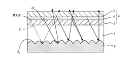
- FIG. 3 shows the light-emitting portion 6, the high refractive index layer 7, the reflective layer 8, and how the light beams 21 and 22 are reflected by these configurations.
- the light beam 21 from the organic layer 4 is reflected by the reflective layer 8 at the same angle as the incident angle, as indicated by a broken line in FIG.
- light incident on the light beam 21 at an angle greater than the critical angle repeats total reflection between the first light-transmissive electrode layer 3 and the reflective layer 8 and is not extracted to the transparent substrate 2 side. End up.
- the light beam 22 from the organic layer 4 is reflected by the reflective layer 8 and the uneven surface as shown by the solid line in FIG. The reflection is repeated by the interface 7b.
- the interface 7b By repeating the reflection, most of the light beam 22 can be incident on the second light transmissive electrode layer 5 at an angle that can be taken out.
- the light emitting element 1 of this example not only the first light transmissive electrode layer 3 but also the second light transmissive electrode layer 5 is used as the light transmissive electrode layer.
- a high refractive index layer 7 is formed on the second light transmissive electrode layer 5, and a reflective layer 8 is further formed thereon.
- the high refractive index layer 7 includes a plurality of uneven interfaces 7b having a high refractive index. Many of the light rays 22 from the organic layer 4 are repeatedly reflected at random by the reflective layer 8 and the uneven interface 7b, and can be incident on the second light-transmissive electrode layer 5 at an angle that can be taken out. Thereby, the extraction efficiency of the light beam 22 to the transparent substrate 2 side can be improved.
- each concave or convex interface of the concavo-convex interface 7b into a shape having a curvature inside the high refractive index layer 7 using a resin having a refractive index higher than that of the transparent substrate, the organic layer 4
- the light beam 22 is easily reflected. Moreover, it becomes easy to reflect the light beam 22 at various angles by making the concave or convex curvatures of the concave-convex interface 7b nonuniform.
- the light emitting device 1 of the present embodiment further includes a reflecting plate 7c whose both surfaces act as reflecting surfaces.
- the reflecting plate 7c is preferably provided in the high refractive index layer 7 so as to extend perpendicularly to the flat interface on the second light transmissive electrode layer 5, and two or more reflecting plates 7c are preferably provided.
- the reflection plates 7c may be provided at equal intervals, or may be provided at any position, for example, the interval becomes wider as the end of the light emitting element 1 is approached.
- the reflection surface of the reflection plate 7 c is provided so as to cross the direction perpendicular to the thickness direction of the high refractive index layer 7.
- the reflecting plate 7c may be a lattice-like body such as a disk-shaped honeycomb structure made of a thin metal plate such as aluminum or silver.
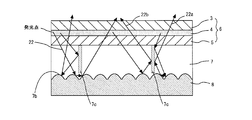
- FIG. 5 shows the second light transmissive electrode layer 5, the high refractive index layer 7, the reflective layer 8, and how light is reflected by these configurations.
- the light beam 22 from the organic layer 4 is reflected not only by the reflection layer 8 and the uneven interface 7b but also by the reflection plate 7c.
- the light rays 22a and 22b which are incident on the second light-transmissive electrode layer 5 at an angle that can be taken out can be increased.
- the extraction efficiency of the light beam 22 to the transparent substrate 2 side can be further improved.
- a light emitting unit 6 including a first light transmissive electrode layer 3, an organic layer 4, and a second light transmissive electrode layer 5 is formed on a transparent substrate 2.
- a first light transmissive electrode layer 3 made of a light transmissive electrode material such as ITO is formed on the transparent substrate 2 made of a light transmissive material such as glass or a resin film, for example, by sputtering.
- a plasma treatment for modifying the surface of the first light transmissive electrode layer 3 may be performed.
- the efficiency of hole injection into the organic layer 4 formed on the first light transmissive electrode layer 3 is improved by performing such plasma treatment. To do.
- an organic layer 4 including a light emitting layer (not shown) containing an organic compound exhibiting electroluminescence characteristics is formed on the first light transmissive electrode layer 3.
- a dry coating method such as a sputtering method or a vacuum deposition method, or a wet coating method such as a screen printing, a spray method, an ink jet method, a spin coating method, a gravure printing, or a roll coater method. It has been known.
- the organic layer material is a low molecular organic compound
- a dry film forming method such as vapor deposition
- a wet method such as spin coating
- a film forming method is used.
- the hole injection layer 4a, the hole transport layer 4b, and the light emitting layer 4c (FIG. 2) are formed by a wet coating method
- the electron transport layer 4d and the electron injection layer 4e are respectively dry-type.
- a film may be sequentially formed by a coating method. Further, all these layers may be sequentially formed by a wet coating method.
- a thin film having a film thickness of the order of nm of magnesium, calcium, potassium, sodium, lithium or an alloy thereof is formed by, for example, vapor deposition, and further, for example, ITO or the like is formed by sputtering.
- a second light transmissive electrode layer 5 made of a light transmissive electrode material is formed.
- an uncured resin layer is formed on the second light-transmissive electrode layer 5 as a high refractive index layer material having a predetermined film thickness by, for example, a spin coating method or an inkjet method. 7d is formed.
- a reflector 7c may be further formed in the high refractive index layer 7 shown in FIG.
- the high refractive index layer 7 including the reflecting plate 7c is, for example, an opaque disk-shaped member made of, for example, aluminum having a height (thickness) less than the thickness of the resin layer 7d on the second light transmitting electrode layer 5. It can be formed by previously bonding the honeycomb structure and injecting an uncured resin thereon.
- an uneven reflection layer 8 having an uneven surface M7 to be an uneven interface is formed in advance on the main surface, and a support substrate 9 is prepared.
- the concavo-convex surface M7 can be formed by, for example, forming a mold in which a reverse shape of the concavo-convex surface is formed in advance using a known surface processing technique, and applying the pressure by overlapping the mold on the flat metal film on the support substrate 9.
- the uneven surface M7 is transferred to the flat metal film.
- the transparent substrate 2 and the support substrate 9 are supported so that the high refractive index layer 7d on the light emitting portion 6 and the reflective layer 8 face each other.
- the transparent substrate 2 and the support substrate 9 are bonded together by the resin layer 7d so that the light emitting portion 6 and the reflective layer 8 are integrated via the resin layer 7d.
- the light emitting element 1 shown in FIG. 1 in which the light emitting unit 6 is hermetically protected by disposing the sealing unit 10 such as an adhesive around the light emitting unit 6 between the transparent substrate 2 and the support substrate 9 is manufactured. .
- the light emitting device 1 of this example uses a plurality of light scattering particles 7 f dispersed in the high refractive index layer 7 as a light scattering structure instead of the uneven interface which is a light scattering structure. .
- the first light-transmissive electrode layer 3 is formed on the transparent substrate 2 and then the organic layer 4 is laminated to form the second light-transmissive electrode layer 5.
- the light emitting part 6 is formed.
- a fluid state resin layer of a high refractive index layer material in which a plurality of light scattering particles 7 f is dispersed is formed on the second light transmissive electrode layer 5.
- the flat reflective layer 8 b is formed on the support substrate 9 in advance. Then, the transparent substrate 2 and the support substrate 9 are bonded together by the high refractive index layer 7 so that the light emitting unit 6 and the flat reflective layer 8 b are integrated via the high refractive index layer 7. At this time, the light emitting device 1 shown in FIG. 7 in which the light emitting portion 6 is hermetically protected by disposing the sealing portion 10 such as an adhesive around the light emitting portion 6 between the transparent substrate 2 and the support substrate 9 is manufactured. .
- each of the plurality of light scattering particles 7f has a refractive index different from that of the high refractive index layer.
- the light scattering particles 7f may be, for example, particles of an inorganic material having a higher refractive index than that of the high refractive index layer 7 such as glass beads or zirconia or titania.
- the light scattering particle 7f has a shape in which the particle surface has a curvature, for example, a spherical shape or an elliptical shape.
- the particle diameter of the light scattering particle 7f is, for example, 10 nm to 200 nm.
- the particle diameter of each of the light scattering particles 7f is uniform or nonuniform.
- Each of the light scattering particles 7f is made of the same material or two or more materials. Further, it is desirable that the light scattering particles 7f be uniformly distributed over the entire high refractive index layer 7. Further, by making the light scattering particles 7f have a spherical shape such as a spherical surface, the light from the organic layer 4 can be easily reflected and refracted. It is also easy to reflect and refract the light from the organic layer 4 by making the particle size of the light scattering particles 7f non-uniform.
- the high refractive index layer 7 includes a plurality of light scattering particles 7f having a high refractive index, but is not limited thereto.
- a high refractive index layer 7 in which a plurality of low refractive index bubbles such as inert gas are dispersed may be used.
- the same effect can be obtained by reflection and refraction of the bubbles, which are light scattering particles, by the light scattering particles 7f.
- the refractive index between the concave and convex reflective layer 8 or the flat reflective layer 8b and the second light transmissive electrode layer 5 is approximately the same as that of the second light transmissive electrode layer 5.
- the light-emitting portion 6 and the reflective layer are integrated by being coupled by a high refractive index layer 7 having the same.
- the reflective layer is supported on a support substrate 9 that is separate from the transparent substrate 2 that supports the light emitting unit 6.
- the organic layer 4 is laminated, and the second light transmissive electrode layer 5 is formed.
- the light emitting unit 6 is formed.
- the uneven reflection layer 8 or the flat reflection layer 8 b having the uneven surface M 7 to be the uneven interface 7 b is formed on the support substrate 9.
- the transparent substrate 2 and the support substrate 9 are bonded together by the high refractive index layer 7 so that the light emitting unit 6 and the reflective layer are integrated via the high refractive index layer 7.
- the sealing unit 10 such as an adhesive around the light emitting unit 6.
- the light emitting device can be manufactured by a simple process, and the light extraction efficiency of the light emitting device can be improved.
- Light emitting element 1 Transparent substrate 2 First light transmissive electrode layer 3 Organic layer 4 Second light transmissive electrode layer 5 Light emitting part 6 High refractive index layer 7 Uneven interface 7b Reflector 7c Reflective layer 8 Support substrate 9 Sealing part 10
Landscapes
- Physics & Mathematics (AREA)
- Optics & Photonics (AREA)
- Electroluminescent Light Sources (AREA)
Description
本発明は、有機エレクトロルミネッセンス素子(以下、有機EL素子と称する)などの発光素子及びその製造方法に関する。
ガラス基板上の陽極と陰極の電極層の間に発光層を含む有機層が挟持された有機EL素子が知られている。この有機EL素子は、陽極と陰極の間に電圧を印加すると電流が流れて発光層が発光する。発光光は例えば陽極を透明とすることによりガラス基板から取り出される。発光層から発せられた光の一部は陽極-ガラス界面間及びガラス-空気界面間での全反射により閉じ込められ消衰する故に、発光層で生成された光のうち約20%程度の光しか外部に取り出すことができず、光取り出し効率が低いという問題がある。
この問題に対して、例えば、光取り出し側のガラス基板に構造体を形成したり(特許文献1、参照)、ガラス基板の最表面に構造体を形成したり(特許文献2、参照)、ガラス基板に構造体を形成したり(特許文献3、参照)、光取り出し側の反対側に素子ごとに凹面鏡を形成したり(特許文献3、参照)、するなど光取り出し効率を向上させる提案がなされてきた。
しかしながら、特許文献1に開示される構造の場合には、有機層内に低屈折率層が存在した場合には、当該低屈折率層と、裏面反射層として作用する陰極層との間が導波路構造になり、光取出し効率を向上させる目的でガラス基板上面に設けられた屈折材料層にまで光が十分に届かないという問題がある。
また、特許文献2に開示される構造の場合には、ガラス基板の光取り出し表面(最表面)に構造体を形成しても、当該基板は有機層よりも遥かに厚いので、光路長が長くなり、発光領域外へ光が導波してしまうという問題がある。
さらに、特許文献3に開示される構造の場合には、ガラス基板と有機層間に構造体を形成しているが故に、その凹凸が有機層の凹凸になってしまい、印加電圧ムラが発生してしまう。それを防ぐために有機EL素子形成面に平坦化処理を行う必要があ
り、プロセスが複雑化するという問題がある。
り、プロセスが複雑化するという問題がある。
さらにまた、特許文献4に開示される構造の場合には、電極の光取り出し側とは逆側に集光タイプの異型処理を行った反射層を設けているが、有機層と反射層の間は空気層であるため屈折率が低く、反射されて素子に戻る際の効率が悪くまた、素子と反射面の中心合わせ工程が必要で、製造歩留まりが悪いという問題がある。
そこで、簡素な構造を有し且つ本発明は上記した如き問題点に鑑みてなされたものであって、光取り出し効率の高い発光素子及びその製造方法を提供することを目的とする。
本発明による発光素子は、発光層を含む有機層と前記有機層を挟む第1及び第2光透過性電極層とからなる発光部と、前記発光部を前記第1光透過性電極層を介して担持する透明基板と、を含む。当該発光素子は、光散乱構造体及び前記透明基板の屈折率より高い屈折率を有しかつ前記第2光透過性電極層に接する高屈折率層と、前記第2光透過性電極層と共に前記高屈折率層を挟む反射層と、前記反射層を担持する支持基板と、を更に有することを特徴とする。
本発明による上記の発光素子の製造方法であって、支持基板上に反射層を形成するステップと、透明基板上に順に積層された第1光透過性電極層、有機層及び第2光透過性電極層からなる発光部を形成するステップと、前記第2光透過性電極層上に高屈折率層材料を積層するステップと、前記高屈折率層を介して、前記第2光透過性電極層と前記反射層とを貼り合わせて前記発光部と前記反射層を一体化するステップと、を含むことを特徴とする。
以下、本発明に係る実施例について添付の図面を参照しつつ詳細に説明する。
<第1の実施例>
図1には、本発明の実施例である有機EL素子の発光素子1の構成が示されている。
図1には、本発明の実施例である有機EL素子の発光素子1の構成が示されている。
発光素子1において、透光性基板2上に、第1光透過性電極層3、有機層4及び第2光透過性電極層5とからなる発光部6が形成されている。次いで、発光部6上に高屈折率層7、反射層8及び支持基板9が順に配置されている。有機層4は、典型的には図2に示されるように、正孔注入層4a、正孔輸送層4b、発光層4c、電子輸送層4d、及び電子注入層4eが積層されて構成される。なお、有機層4の積層構成において、基板以外の構成要素を逆の順に積層することも可能である。いずれにしても、有機層4は発光積層体であり、これら積層構成に限定されることなく、少なくとも発光層を含み、或いは兼用できる電荷輸送層を含む積層構成も本発明に含まれる。有機層4は、上記積層構造から正孔輸送層4bを省いて構成しても、正孔注入層4aを省いて構成しても、正孔注入層4aと電子輸送層4dを省いて構成してもよい。
発光層4cは、有機EL材料からなる。有機EL材料としては、例えば、蛍光材料や燐光材料などの任意の公知の材料を適用可能である。
青色発光を与える蛍光材料としては、例えば、ナフタレン、ペリレン、ピレンなどが挙げられる。緑色発光を与える蛍光材料としては、例えば、キナクリドン誘導体、クマリン誘導体、Alq3(tris (8-hydroxy-quinoline) aluminum) などのアルミニウム錯体などが挙げられる。黄色発光を与える蛍光材料としては、例えば、ルブレン、ペリミドン誘導体などが挙げられる。赤色発光を与える蛍光材料としては、例えば、DCM(4-(dicyanomethylene)-2-methyl-6-(p-dimethylaminostyryl)-4H-pyran)系化合物、ベンゾピラン誘導体、ローダミン誘導体などが挙げられる。燐光材料としては、例えば、ルテニウム、ロジウム、パラジウムなどが挙げられる。燐光材料として、具体的には、トリス(2-フェニルピリジン)イリジウム(所謂、Ir(ppy)3)、トリス(2-フェニルピリジン)ルテニウム、などが挙げられる。
有機層4の一方の面上には第1光透過性電極層3が形成され、他方の面上には第2光透過性電極層5が形成されている。第1光透過性電極層3は陽極であり、第2光透過性電極層5は陰極である。第1光透過性電極層3及び第2光透過性電極層5の各々は、光透過性電極層からなる。例えばITO(Indium-tin-oxide)やFTO(fluorine-tin-oxide)が光透過性電極材料として用いられる。また、ZnO、ZnO-Al2O3(所謂、AZO)、InGaZnOx(所謂IGZO)、In2O3-ZnO(所謂、IZO)、SnO2-Sb2O3(所謂、ATO)、RuO2などの酸化物系材料を用いることもできる。第1光透過性電極層3及び第2光透過性電極層5は、有機層4を挟む位置に存在する。
なお、電子を供給する陰極の第2光透過性電極層5の材料としては、効率良く電子注入を行う為に仕事関数の低い金属が好ましく、例えば、スズ、マグネシウム、インジウム、カルシウム、アルミニウム、銀などの適当な金属又はそれらの合金が用いられる。具体例としては、マグネシウム-銀合金、マグネシウム-インジウム合金、アルミニウム-リチウム合金などの低仕事関数合金電極が挙げられる。
第2光透過性電極層5には、106S/m以上の電気伝導率を有する電気伝導体からなり、可視光の最短波長の略360nm以下すなわち、超軟X線から紫外線の波長の範囲の膜厚を有する薄膜を、上記酸化物系材料や金属系の薄膜に積層して用いることができる。第2光透過性電極層5と積層する当該薄膜の材料には、金属やグラファイト、グラフェン(graphene)などの炭素が含まれる。第2光透過性電極層5の薄膜としての膜厚20nmの銀薄膜は透過率50%を有する。同薄膜としての膜厚10nmのAl膜は透過率50%を有する。同薄膜としての膜厚20nmのMgAg合金膜は透過率50%を有する。透光性導電薄膜は、電気伝導体からなり且つ超軟X線から紫外線の波長の範囲の膜厚を有する薄膜の膜厚を有し且つ少なくとも50%の透過率を有する薄膜を採用することが好ましい。なお、薄膜で第2光透過性電極層5を構成する場合、その薄膜膜厚の下限値は1nmあれば導電性を確保することができる。
透明基板2は、第1光透過性電極層3を介して発光部6を担持している。透明基板2は、例えばガラスやポリエステル、ポリメタクリレート、ポリカーボネート、ポリスルホンなどの樹脂フィルムなどの光透過性材料からなる。発光部6から発せられた光20が透明基板2を介して出力される。
第2光透過性電極層5上には高屈折率層7が形成されている。高屈折率層7は、第2光透過性電極層5に平坦界面にて接している。高屈折率層7の材料としては、例えばアクリル系、エポキシ系、スチレン系の化合物樹脂や、それらに酸化チタン、酸化ニオブ、酸化タンタル、酸化ジルコニウム、酸化セリウム等の金属酸化物等のナノパーティクルを添加した透過性材料が用いられ、透明基板2の屈折率より高い屈折率を有するものから選択される。さらに、高屈折率層7は光線が第2光透過性電極層5との界面での反射を低く抑えるために第2光透過性電極層5の屈折率の±30%以内の範囲の屈折率を有するものから選択されることが望ましい。
透明基板2の屈折率は例えば1.5である。有機層4の屈折率は例えば1.0~1.8である。第1光透過性電極層3及び第2光透過性電極層5の各々の屈折率は例えば1.8~2.0である。高屈折率層7の屈折率は例えば、1.26~2.6である。
高屈折率層7上には光散乱構造体である凹凸界面7bを介して反射層8が配置されている。すなわち、高屈折率層7に接触する反射層8には凹凸界面7bが形成されている。複数の凹部と凸部からなる凹凸界面7bは例えばマイクロレンズアレイ形状界面である。なお、凹凸界面7bは所定の粗面であればよく、マイクロレンズアレイ形状の他にピラミッドアレイ形状、V溝形状、V溝形状、鋸形状、ピラーアレイ形状などを含む非平坦界面となる凹凸面である。さらに、マイクロレンズアレイ形状やピラミッドアレイ形状などの場合、凹凸界面7bは、高屈折率層7側に各々レンズやピラミッドが凸である形状の他に、各々レンズやピラミッドが凹である凹面鏡として構成しても良い。反射層8は、第2光透過性電極層5と共に高屈折率層7を挟んでいる。反射層8の材料としては、例えばアルミニウムや銀などの金属が用いられる。なお、反射層8の反射作用を維持する厚さであれば膜厚は限定されない。一方、高屈折率層7の厚さは例えば1μm~50μmである。高屈折率層7の膜厚はこれに限られず、凹凸界面7bの各凹又は凸の各深さ又は高さの最大値を超えれば適宜定めることができる。また、凹凸界面7bは、高屈折率層7内に均一に且つ全体に亘って分布していることが望ましい。
凹凸界面7bの複数のマイクロレンズ形状や大きさが同一に形成されてもよい。また、凹凸界面7bのそれぞれのマイクロレンズ形状、大きさ、高さはランダムに構成してもよい。かかるマイクロレンズのランダム配置の場合はランダムな反射が得られ光の散乱効果を大きくする。なお、マイクロレンズは、隣接するもの同士の間に間隙を有して配置してもよい。
発光素子1の製造工程においては、透明基板2上に第1光透過性電極層3を成膜後、有機層4を積層して、第2光透過性電極層5を形成して、発光部6が形成される。一方、凹凸界面7bとなるべき凹凸表面を備えた凹凸反射層8が支持基板9上に予め形成される。そして、発光部6と当該反射層8とが高屈折率層7を介して一体化するように、透明基板2と支持基板9を高屈折率層7により貼り合わせる。このとき、透明基板2と支持基板9の間の発光部6の周囲に接着剤などの封止部10を配置することにより発光部6を密閉保護した図1に示す発光素子1が製造される。
高屈折率層7は第2光透過性電極層5と同等の屈折率を有することで光学的に発光部6と凹凸界面7bとを結合させると共に、物理的にも接着層として機能させることも可能である。
本実施例によれば、発光部6とは別プロセスにて凹凸界面7bとなるべき凹凸表面を反射層8に形成することができる。これにより、凹凸界面を形成するプロセスに起因する高屈折率層7から発光部6への出ガスなどによる影響が低減可能なため、高屈折率層の材料選択の幅を拡げることができる。また、発光部6と反射層8の間の高屈折率層7を薄膜化することで、光取り出しにおける多重反射時の光路長を短くすることができる。よって、高屈折率層7の薄膜化は光減衰の点で有利である。同様に凹凸界面7bもサブミクロンオーダーの小さなものでも、大きな光路変更効果が見込める。高屈折率層7の薄膜化は製造工程におけるプロセス処理時間の短縮効果の点でも有利である。
図3には、発光部6、高屈折率層7、反射層8、及びこれらの構成による光線21及び22の反射の様子が示されている。
仮に、凹凸界面7bが存在しない場合には、図3に破線で示されるように、有機層4からの光線21は反射層8で入射角と同じ角度で反射する。その結果、光線21のうち、臨界角以上の角度で入射する光は、第1光透過性電極層3と反射層8との間で全反射を繰り返して、透明基板2側には取り出されなくなってしまう。
これに対して、凹凸界面7bを有する高屈折率層7を有する本実施例の発光素子1においては、図3に実線で示されるように、有機層4からの光線22は反射層8及び凹凸界面7bにより反射を繰り返す。反射の繰り返しにより、光線22の大部分が第2光透過性電極層5に対して取出し可能な角度で入射し得る。
上記したように、本実施例の発光素子1においては、第1光透過性電極層3のみならず、第2光透過性電極層5をも光透過性電極層としている。そして、第2光透過性電極層5上には高屈折率層7と、更に、その上に反射層8が形成されている。高屈折率層7は、複数の高屈折率の凹凸界面7bを含んでいる。有機層4からの光線22の多くは反射層8及び凹凸界面7bによりランダムに反射を繰り返し、第2光透過性電極層5に対して取出し可能な角度で入射し得る。これにより、透明基板2側への光線22の取出し効率を向上させることができる。
透明基板の屈折率よりも高い屈折率の樹脂などを用いた高屈折率層7の内部にて、凹凸界面7bの各凹又は凸の界面を曲率を有する形状とすることにより、有機層4からの光線22を反射させ易くなる。また、凹凸界面7bの各凹又は凸の曲率を不均一とすることによっても光線22を様々な角度で反射させ易くなる。
<第2の実施例>
以下、第2の実施例について第1の実施例と異なる部分について主に説明する。
以下、第2の実施例について第1の実施例と異なる部分について主に説明する。
図4には、本実施例の発光素子1は、両面が反射面として作用する反射板7cを更に含む。反射板7cは、第2光透過性電極層5に平坦界面に対し垂直に拡がるように高屈折率層7内に設けられ、2つ以上の反射板7cが設けられることが望ましい。この場合、反射板7cは、等間隔に設けられても良いし、例えば発光素子1の端部に近付く程間隔が広くなるなど任意の位置に設けることができる。反射板7cの反射面は、高屈折率層7の厚さ方向に垂直な方向をよぎるように設けられている。反射板7cは例えばアルミニウムや銀などの金属の薄板からなる盤状のハニカム構造体などの格子状体でもよい。
図5には、第2光透過性電極層5、高屈折率層7、反射層8、及びこれらの構成による光線の反射の様子が示されている。有機層4からの光線22は、反射層8及び凹凸界面7bのみならず、反射板7cによっても反射される。これにより、第2光透過性電極層5に対して取出し可能な角度で入射する光線22a及び22bを増加させることができる。これにより、透明基板2側への光線22の取出し効率を更に向上させることができる。
<発光素子の製造方法>
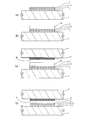
以下、図6を参照しつつ、発光素子1の製造方法について説明する。
以下、図6を参照しつつ、発光素子1の製造方法について説明する。
先ず、図6(a)に示すように、透明基板2上に第1光透過性電極層3、有機層4、及び第2光透過性電極層5からなる発光部6を形成する。
例えばガラスや樹脂フィルムなどの光透過性材料からなる透明基板2上に、例えばスパッタリング法により、例えばITOなどの光透過性電極材料からなる第1光透過性電極層3を成膜する。なお、第1光透過性電極層3の形成後に、第1光透過性電極層3の表面を改質するためのプラズマ処理が行われても良い。例えば、第1光透過性電極層3がITOからなる場合、かかるプラズマ処理を施すことによって、この後に第1光透過性電極層3上に形成される有機層4への正孔注入効率が向上する。
そして、第1光透過性電極層3上に、エレクトロルミネセンス特性を呈する有機化合物を含有する発光層(図示せず)を含む有機層4を形成する。有機ELパネルの機能層を成膜する手法として、スパッタリング法や真空蒸着法などの乾式塗布法や、スクリーン印刷、スプレイ法、インクジェット法、スピンコート法、グラビア印刷、ロールコータ法などの湿式塗布法が知られている。一般的に、有機層の材料が低分子有機化合物である場合には蒸着法などの乾式成膜法が用いられ、有機層の材料が高分子有機化合物である場合にはスピンコート法などの湿式成膜法が用いられる。また、例えば、正孔注入層4a、正孔輸送層4b、発光層4c(図2)を湿式塗布法により成膜して、電子輸送層4d及び電子注入層4e(図2)を、それぞれ乾式塗布法により順次成膜しても良い。また、これらの全ての層を湿式塗布法により順次成膜しても良い。
そして、有機層4上に、例えば蒸着法などにより、マグネシウム、カルシウム、カリウム、ナトリウム、リチウム又はこれらの合金の膜厚nmオーダーの薄膜を成膜し、さらに、スパッタリング法などにより、例えばITOなどの光透過性電極材料からなる第2光透過性電極層5を成膜する。
次に、図6(b)に示すように、第2光透過性電極層5上に、例えばスピンコート法、インクジェット法などにより、所定膜厚の高屈折率層材料として例えば未硬化の樹脂層7dを成膜する。なお、この工程において図4に示す高屈折率層7内に反射板7cを更に形成しても良い。反射板7cを含む高屈折率層7は、例えば、第2光透過性電極層5上に樹脂層7dの厚さ未満の高さ(厚さ)を有する例えばアルミニウムなどからなる不透明な盤状のハニカム構造体を予め接着しておいて、その上から未硬化の樹脂を注入することにより形成することができる。
次に、図6(c)に示すように、凹凸界面となるべき凹凸表面M7を備えた凹凸反射層8が主面上に予め形成され支持基板9を用意する。凹凸表面M7は、例えば、公知の表面加工技術を用いて当該凹凸表面の反転形状を形成したモールドを予め形成して、該モールドを支持基板9上の平坦金属膜に重ねて圧力をかければ、凹凸表面M7が平坦金属膜に転写される。
次に、図6(c)に示すように、発光部6上の高屈折率層7dと反射層8とが対向するように、透明基板2と支持基板9透明基板2を支持する。
次に、図6(d)に示すように、発光部6と反射層8とが樹脂層7dを介して一体化するように、透明基板2と支持基板9を樹脂層7dにより貼り合わせる。このとき、透明基板2と支持基板9の間の発光部6の周囲に接着剤などの封止部10を配置することにより発光部6を密閉保護した図1に示す発光素子1が製造される。
<第3の実施例>
以下、第3の実施例について第1の実施例と異なる部分について主に説明する。
以下、第3の実施例について第1の実施例と異なる部分について主に説明する。
図7には、本実施例の発光素子1は、光散乱構造体である凹凸界面に代えて光散乱構造体として高屈折率層内7に分散された複数の光散乱粒子7fを用いている。
高屈折率層7と平坦反射層8bの界面に複数の光散乱粒子7fを配置することで、第1の実施例の反射層8の凹凸界面7bの代わりとすることも可能である。
本実施例の発光素子1の製造工程においては、透明基板2上に第1光透過性電極層3を成膜後、有機層4を積層して、第2光透過性電極層5を形成して、発光部6が形成される。複数の光散乱粒子7fが分散された高屈折率層材料の流動体状態の樹脂層が第2光透過性電極層5上に成膜される。一方、平坦反射層8bが支持基板9上に予め形成される。そして、発光部6と当該平坦反射層8bとが高屈折率層7を介して一体化するように、透明基板2と支持基板9を高屈折率層7により貼り合わせる。このとき、透明基板2と支持基板9の間の発光部6の周囲に接着剤などの封止部10を配置することにより発光部6を密閉保護した図7に示す発光素子1が製造される。
光散乱粒子7fを配する本実施例の場合、反射層8bに直接加工する必要が無くなるため、製造の歩留まり向上が期待できる。複数の光散乱粒子7fの各々は高屈折率層の屈折率と異なる屈折率を有する。光散乱粒子7fは、例えば、ガラスビーズや、あるいはジルコニア、チタニアなどの高屈折率層7より高い屈折率の無機材料の粒子でもよい。光散乱粒子7fは、例えば球形や楕円形などの粒子表面が曲率を有する形状からなる。光散乱粒子7fの粒径は例えば10nm~200nmである。光散乱粒子7fの各々の粒径は均一又は不均一である。また、光散乱粒子7fの各々は、同一の材料又は2以上の材料からなる。また、光散乱粒子7fは、高屈折率層7の全体に亘って均一分布していることが望ましい。また、光散乱粒子7fを球形などの粒子表面が曲率を有する形状とすることにより、有機層4からの光線を反射及び屈折させ易くなる。光散乱粒子7fの粒径を不均一とすることによっても有機層4からの光線を反射及び屈折させ易くなる。
また、上記の実施例は、高屈折率層7が複数の高屈折率の光散乱粒子7fを含む場合の例であるが、これに限られない。光散乱粒子7fとして不活性ガスなどの複数の低屈折率の気泡を分散させた高屈折率層7用いてもよい。この場合にも光散乱粒子である当該気泡の光散乱粒子7fによる反射及び屈折により、同様の効果を奏することができる。
以上のように、上記の実施例に何れによっても、凹凸反射層8又は平坦反射層8bと第2光透過性電極層5の間は第2光透過性電極層5と同程度の屈折率を有する高屈折率層7で結合されて発光部6と前記反射層が一体化されている。また、前記反射層は発光部6を担持する透明基板2とは別体の支持基板9上に担持されている。
また、上記の実施例の方法によれば、透明基板2上に第1光透過性電極層3を成膜後、有機層4を積層し、第2光透過性電極層5を形成して、発光部6が形成される。一方、凹凸界面7bとなるべき凹凸表面M7を備えた凹凸反射層8、もしくは平坦反射層8bを支持基板9上に形成する。発光部6と当該反射層とが高屈折率層7を介して一体化するように、透明基板2と支持基板9を高屈折率層7により貼り合わせる。このとき発光部6の周囲に接着剤などの封止部10を配置することにより発光部6を密閉保護することが可能となる。
よって本発明による発光素子及びその製造方法によれば、簡素な工程で製造でき、発光素子の光取り出し効率を向上させることができる。
発光素子1
透明基板2
第1光透過性電極層3
有機層4
第2光透過性電極層5
発光部6
高屈折率層7
凹凸界面7b
反射板7c
反射層8
支持基板9
封止部10
透明基板2
第1光透過性電極層3
有機層4
第2光透過性電極層5
発光部6
高屈折率層7
凹凸界面7b
反射板7c
反射層8
支持基板9
封止部10
Claims (7)
- 発光層を含む有機層と前記有機層を挟む第1及び第2光透過性電極層とからなる発光部と、前記発光部を前記第1光透過性電極層を介して担持する透明基板と、を含む発光素子であって、
光散乱構造体及び前記透明基板の屈折率より高い屈折率を有しかつ前記第2光透過性電極層に接する高屈折率層と、前記第2光透過性電極層と共に前記高屈折率層を挟む反射層と、前記反射層を担持する支持基板と、を更に有することを特徴とする発光素子。 - 前記光散乱構造体は、前記高屈折率層及び前記反射層の間の凹凸界面であって、前記凹凸界面が非平坦界面であることを特徴とする請求項1に記載の発光素子。
- 前記光散乱構造体は、前記高屈折率層内に分散された複数の光散乱粒子であって、前記光散乱粒子の各々が前記高屈折率層の屈折率と異なる屈折率を有することを特徴とする請求項1に記載の発光素子。
- 前記高屈折率層は、前記第2光透過性電極層の屈折率の±30%以内の範囲の屈折率を有することを特徴とする請求項2乃至請求項3に記載の発光素子。
- 前記高屈折率層は、その厚さ方向に垂直な方向をよぎる両面が反射面として作用する少なくとも1つの反射部を更に含むことを特徴とする請求項2乃至請求項3に記載の発光素子。
- 発光層を含む有機層と前記有機層を挟む第1及び第2光透過性電極層とからなる発光部と、前記発光部を前記第1光透過性電極層を介して担持する透明基板と、光散乱構造体及び前記透明基板の屈折率より高い屈折率を有しかつ前記第2光透過性電極層に接する高屈折率層と、前記第2光透過性電極層と共に前記高屈折率層を挟む反射層とを有する発光素子の製造方法であって、
支持基板上に反射層を形成するステップと、
透明基板上に順に積層された第1光透過性電極層、有機層及び第2光透過性電極層からなる発光部を形成するステップと、
前記第2光透過性電極層上に高屈折率層材料の流動体状態の樹脂層を成膜するステップと、
前記樹脂層を介して、前記第2光透過性電極層と前記反射層とを貼り合わせて前記発光部と前記反射層を一体化するステップと、を含むことを特徴とする発光素子の製造方法。 - 前記支持基板と前記透明基板とを封止部を介して接合して前記発光部を密閉するステップと、を更に含むことを特徴とする請求項6に記載の有機EL発光素子の製造方法。
Priority Applications (1)
| Application Number | Priority Date | Filing Date | Title |
|---|---|---|---|
| PCT/JP2012/060932 WO2013161002A1 (ja) | 2012-04-24 | 2012-04-24 | 発光素子及びその製造方法 |
Applications Claiming Priority (1)
| Application Number | Priority Date | Filing Date | Title |
|---|---|---|---|
| PCT/JP2012/060932 WO2013161002A1 (ja) | 2012-04-24 | 2012-04-24 | 発光素子及びその製造方法 |
Publications (1)
| Publication Number | Publication Date |
|---|---|
| WO2013161002A1 true WO2013161002A1 (ja) | 2013-10-31 |
Family
ID=49482373
Family Applications (1)
| Application Number | Title | Priority Date | Filing Date |
|---|---|---|---|
| PCT/JP2012/060932 Ceased WO2013161002A1 (ja) | 2012-04-24 | 2012-04-24 | 発光素子及びその製造方法 |
Country Status (1)
| Country | Link |
|---|---|
| WO (1) | WO2013161002A1 (ja) |
Citations (5)
| Publication number | Priority date | Publication date | Assignee | Title |
|---|---|---|---|---|
| JP2002231444A (ja) * | 2001-01-30 | 2002-08-16 | Toppan Printing Co Ltd | 高分子el素子およびその製造方法 |
| JP2003303677A (ja) * | 2002-04-09 | 2003-10-24 | Dainippon Printing Co Ltd | 自発光素子 |
| JP2006294491A (ja) * | 2005-04-13 | 2006-10-26 | Seiko Epson Corp | エレクトロルミネッセンス装置、エレクトロルミネッセンス装置の製造方法、電子機器 |
| WO2009131019A1 (ja) * | 2008-04-22 | 2009-10-29 | 日本ゼオン株式会社 | 有機エレクトロルミネッセンス光源装置 |
| JP2010182449A (ja) * | 2009-02-03 | 2010-08-19 | Fujifilm Corp | 有機el表示装置 |
-
2012
- 2012-04-24 WO PCT/JP2012/060932 patent/WO2013161002A1/ja not_active Ceased
Patent Citations (5)
| Publication number | Priority date | Publication date | Assignee | Title |
|---|---|---|---|---|
| JP2002231444A (ja) * | 2001-01-30 | 2002-08-16 | Toppan Printing Co Ltd | 高分子el素子およびその製造方法 |
| JP2003303677A (ja) * | 2002-04-09 | 2003-10-24 | Dainippon Printing Co Ltd | 自発光素子 |
| JP2006294491A (ja) * | 2005-04-13 | 2006-10-26 | Seiko Epson Corp | エレクトロルミネッセンス装置、エレクトロルミネッセンス装置の製造方法、電子機器 |
| WO2009131019A1 (ja) * | 2008-04-22 | 2009-10-29 | 日本ゼオン株式会社 | 有機エレクトロルミネッセンス光源装置 |
| JP2010182449A (ja) * | 2009-02-03 | 2010-08-19 | Fujifilm Corp | 有機el表示装置 |
Similar Documents
| Publication | Publication Date | Title |
|---|---|---|
| KR101471501B1 (ko) | 면상 발광 장치 | |
| US8890136B2 (en) | Planar light emitting device | |
| US8987767B2 (en) | Light emitting device having improved light extraction efficiency | |
| CN111834545A (zh) | 显示面板和显示装置 | |
| TWI517473B (zh) | 有機電致發光裝置,照明器具裝置,及用於製造有機電致發光裝置之方法 | |
| JP5523870B2 (ja) | 面発光素子 | |
| JP5179392B2 (ja) | 有機el発光装置 | |
| WO2013051633A1 (ja) | 発光装置 | |
| CN101176214A (zh) | 电致发光光源 | |
| JP2013054837A (ja) | 発光装置及びその製造方法 | |
| JP5421843B2 (ja) | 発光装置 | |
| WO2013042784A1 (ja) | 発光装置 | |
| JP5452691B2 (ja) | 発光装置 | |
| KR102538050B1 (ko) | 광 추출 장치 및 oled 디스플레이 | |
| WO2013161000A1 (ja) | 発光素子及びその製造方法 | |
| US10763456B2 (en) | EL device use front plate and lighting device | |
| KR20140074446A (ko) | 광추출 효율이 향상된 발광 소자 및 그 제조 방법 | |
| WO2013065177A1 (ja) | 発光装置 | |
| WO2013161002A1 (ja) | 発光素子及びその製造方法 | |
| JP6488593B2 (ja) | 照明装置 | |
| CN111599932B (zh) | 一种oled显示面板及oled显示器 | |
| WO2013161001A1 (ja) | 有機el発光素子 | |
| WO2013190623A1 (ja) | エレクトロルミネッセンス素子 | |
| WO2013190621A1 (ja) | エレクトロルミネッセンス素子 | |
| WO2013065172A1 (ja) | 発光装置および発光装置の製造方法 |
Legal Events
| Date | Code | Title | Description |
|---|---|---|---|
| 121 | Ep: the epo has been informed by wipo that ep was designated in this application |
Ref document number: 12875124 Country of ref document: EP Kind code of ref document: A1 |
|
| NENP | Non-entry into the national phase |
Ref country code: DE |
|
| 122 | Ep: pct application non-entry in european phase |
Ref document number: 12875124 Country of ref document: EP Kind code of ref document: A1 |
|
| NENP | Non-entry into the national phase |
Ref country code: JP |