WO2013147010A1 - 有機elパネル - Google Patents
有機elパネル Download PDFInfo
- Publication number
- WO2013147010A1 WO2013147010A1 PCT/JP2013/059232 JP2013059232W WO2013147010A1 WO 2013147010 A1 WO2013147010 A1 WO 2013147010A1 JP 2013059232 W JP2013059232 W JP 2013059232W WO 2013147010 A1 WO2013147010 A1 WO 2013147010A1
- Authority
- WO
- WIPO (PCT)
- Prior art keywords
- organic
- conductive member
- panel
- contact
- power feeding
- Prior art date
- Legal status (The legal status is an assumption and is not a legal conclusion. Google has not performed a legal analysis and makes no representation as to the accuracy of the status listed.)
- Ceased
Links
Images













Classifications
-
- F—MECHANICAL ENGINEERING; LIGHTING; HEATING; WEAPONS; BLASTING
- F21—LIGHTING
- F21V—FUNCTIONAL FEATURES OR DETAILS OF LIGHTING DEVICES OR SYSTEMS THEREOF; STRUCTURAL COMBINATIONS OF LIGHTING DEVICES WITH OTHER ARTICLES, NOT OTHERWISE PROVIDED FOR
- F21V23/00—Arrangement of electric circuit elements in or on lighting devices
- F21V23/06—Arrangement of electric circuit elements in or on lighting devices the elements being coupling devices, e.g. connectors
-
- F—MECHANICAL ENGINEERING; LIGHTING; HEATING; WEAPONS; BLASTING
- F21—LIGHTING
- F21V—FUNCTIONAL FEATURES OR DETAILS OF LIGHTING DEVICES OR SYSTEMS THEREOF; STRUCTURAL COMBINATIONS OF LIGHTING DEVICES WITH OTHER ARTICLES, NOT OTHERWISE PROVIDED FOR
- F21V19/00—Fastening of light sources or lamp holders
-
- H—ELECTRICITY
- H01—ELECTRIC ELEMENTS
- H01R—ELECTRICALLY-CONDUCTIVE CONNECTIONS; STRUCTURAL ASSOCIATIONS OF A PLURALITY OF MUTUALLY-INSULATED ELECTRICAL CONNECTING ELEMENTS; COUPLING DEVICES; CURRENT COLLECTORS
- H01R33/00—Coupling devices specially adapted for supporting apparatus and having one part acting as a holder providing support and electrical connection via a counterpart which is structurally associated with the apparatus, e.g. lamp holders; Separate parts thereof
- H01R33/05—Two-pole devices
- H01R33/18—Two-pole devices having only abutting contacts
-
- F—MECHANICAL ENGINEERING; LIGHTING; HEATING; WEAPONS; BLASTING
- F21—LIGHTING
- F21S—NON-PORTABLE LIGHTING DEVICES; SYSTEMS THEREOF; VEHICLE LIGHTING DEVICES SPECIALLY ADAPTED FOR VEHICLE EXTERIORS
- F21S8/00—Lighting devices intended for fixed installation
- F21S8/04—Lighting devices intended for fixed installation intended only for mounting on a ceiling or the like overhead structures
-
- F—MECHANICAL ENGINEERING; LIGHTING; HEATING; WEAPONS; BLASTING
- F21—LIGHTING
- F21Y—INDEXING SCHEME ASSOCIATED WITH SUBCLASSES F21K, F21L, F21S and F21V, RELATING TO THE FORM OR THE KIND OF THE LIGHT SOURCES OR OF THE COLOUR OF THE LIGHT EMITTED
- F21Y2105/00—Planar light sources
-
- F—MECHANICAL ENGINEERING; LIGHTING; HEATING; WEAPONS; BLASTING
- F21—LIGHTING
- F21Y—INDEXING SCHEME ASSOCIATED WITH SUBCLASSES F21K, F21L, F21S and F21V, RELATING TO THE FORM OR THE KIND OF THE LIGHT SOURCES OR OF THE COLOUR OF THE LIGHT EMITTED
- F21Y2115/00—Light-generating elements of semiconductor light sources
- F21Y2115/10—Light-emitting diodes [LED]
- F21Y2115/15—Organic light-emitting diodes [OLED]
-
- F—MECHANICAL ENGINEERING; LIGHTING; HEATING; WEAPONS; BLASTING
- F21—LIGHTING
- F21Y—INDEXING SCHEME ASSOCIATED WITH SUBCLASSES F21K, F21L, F21S and F21V, RELATING TO THE FORM OR THE KIND OF THE LIGHT SOURCES OR OF THE COLOUR OF THE LIGHT EMITTED
- F21Y2115/00—Light-generating elements of semiconductor light sources
- F21Y2115/20—Electroluminescent [EL] light sources
-
- H—ELECTRICITY
- H01—ELECTRIC ELEMENTS
- H01R—ELECTRICALLY-CONDUCTIVE CONNECTIONS; STRUCTURAL ASSOCIATIONS OF A PLURALITY OF MUTUALLY-INSULATED ELECTRICAL CONNECTING ELEMENTS; COUPLING DEVICES; CURRENT COLLECTORS
- H01R12/00—Structural associations of a plurality of mutually-insulated electrical connecting elements, specially adapted for printed circuits, e.g. printed circuit boards [PCB], flat or ribbon cables, or like generally planar structures, e.g. terminal strips, terminal blocks; Coupling devices specially adapted for printed circuits, flat or ribbon cables, or like generally planar structures; Terminals specially adapted for contact with, or insertion into, printed circuits, flat or ribbon cables, or like generally planar structures
- H01R12/70—Coupling devices
- H01R12/71—Coupling devices for rigid printing circuits or like structures
- H01R12/72—Coupling devices for rigid printing circuits or like structures coupling with the edge of the rigid printed circuits or like structures
- H01R12/721—Coupling devices for rigid printing circuits or like structures coupling with the edge of the rigid printed circuits or like structures cooperating directly with the edge of the rigid printed circuits
Definitions
- the present invention relates to an organic EL (Electro Luminescence) panel mainly used as illumination.
- organic EL panels have attracted attention as a lighting device that can replace incandescent and fluorescent lamps, and many studies have been made.
- the organic EL panel is obtained by attaching accessories such as a frame to an organic EL device having a planar shape.
- the organic EL device is formed by laminating an organic EL element on a substrate such as a glass substrate, a transparent resin film, or a metal sheet, and forming a power feeding structure for feeding power to the organic EL element.
- an organic EL element makes two electrodes which one or both have translucency oppose, and laminated
- the organic EL device emits light by the energy of recombination of electrically excited electrons and holes.
- the organic EL panel is a self-luminous device and can emit light of various wavelengths by appropriately selecting the material of the light emitting layer.
- the organic EL panel has a feature that the thickness is extremely small and lighter than incandescent lamps, fluorescent lamps, and LED lighting, and light is emitted in a planar shape.
- the organic EL panel has higher luminous efficiency than incandescent lamps and fluorescent lamps, the organic EL panel has features that it consumes less power and generates less heat.
- an anisotropic conductive film (anisotropic conductive film) (ACF) is thermocompression bonded to an electrode as a conductive member with low-temperature heat, and connected to a flexible wiring board (FPC).
- the external power supply and the organic EL panel are electrically connected. That is, a method is adopted in which ACF is used as an adhesive between the FPC and the electrode and power is supplied from an external power source to the organic EL panel via the FPC.
- ACF anisotropic conductive film
- FPC flexible wiring board
- an object of the present invention is to provide an organic EL panel that can reliably supply power to the organic EL device from the outside of the organic EL panel.
- two electrode layers and an organic light-emitting layer sandwiched between the electrode layers are laminated on a substrate having a planar shape, and at least one plane serves as a light-emitting surface.
- the organic EL panel having an organic EL device and a frame member that covers at least one side of the base material, the organic EL device has a power feeding portion that is electrically connected to the electrode layer, and the frame member has an opening.
- the current-carrying member is composed of one or a plurality of conductive members, and a part of the current-carrying member is on the organic EL device side
- the frame member covers part or all of the power supply unit, the frame member presses the power supply member against the power supply unit of the organic EL device, and the other part of the power supply member is the opening or notch. Projecting outside the frame member via An organic EL panel according to symptoms.
- the other one part of the said electricity supply member has protruded to the outer side of the frame member via the said opening or notch.
- the other part of the energization member is in a state of being inserted through the opening or notch, and a part of the energization member is exposed outside the frame member. Therefore, by connecting an external power source to the exposed portion of the energization member, it is possible to supply power to the organic EL device from the outside of the organic EL panel via the energization member.
- a part of said electricity supply member exists in the organic EL apparatus side, and has covered a part or all of the said electric power feeding part, and a frame member is used as the electric power feeding part of an organic EL apparatus. Is pressed.
- the energization member is always pressed against the power supply unit of the organic EL device by the frame member and is in contact with the power supply unit. For this reason, the power feeding unit of the organic EL device and the energization member can always be maintained in contact with each other and can be electrically connected.
- no heat is generated during assembly, and the organic light emitting layer is not thermally affected. Therefore, thermal influence on the organic EL panel can be prevented, and power can be reliably supplied to the organic EL device from the outside of the organic EL panel.
- the organic EL panel having an organic EL device that is a surface and a frame member that covers at least one side of the base material
- the organic EL device has a power feeding portion electrically connected to the electrode layer
- the frame has an opening or a notch
- a current-carrying member composed of one or a plurality of conductive members having electrical conductivity, and a part of the current-carrying member is a part of the power feeding unit or
- the frame member covers the whole, and the frame member presses the current-carrying member against the power feeding portion of the organic EL device, and the other part of the current-carrying member is exposed from the opening or notch. It is an organic EL panel.
- Still another invention for solving the same problem is that a substrate having a planar shape is laminated with two electrode layers and an organic light emitting layer sandwiched between the electrode layers, and at least one plane emits light.
- the organic EL panel having an organic EL device that is a surface and a frame member that covers at least one side of the base material
- the organic EL device has a power feeding portion electrically connected to the electrode layer
- the frame has an opening or a notch, has a current-carrying member having electrical conductivity, the current-carrying member has a metal exposed portion having a planar extension, and the power feeding portion is also planar.
- Characteristic organic EL Is Le.
- the above-described organic EL panel has an outer frame member that covers the outer side of the frame member, and a first conductive member that can be electrically connected to an external power source.
- a space is formed, and the first conductive member is disposed in the space and extends in the extending direction of the space, and a part of the energizing member enters the space. However, it is desirable to be in contact with the first conductive member.
- the first conductive member is a member that is connected to an external power source and transmits power to the organic EL device. Therefore, the above-described invention has an outer frame member that covers the outer side of the frame member, and a conductive member for power transmission that can be electrically connected to an external power source, and a predetermined amount is provided between the outer frame member and the frame member. A space is formed, the conductive member for power transmission is disposed in the space, and extends in the extending direction of the space, and a part of the energizing member enters the space. However, the structure is in contact with the conductive member for power transmission.
- a predetermined space is formed between the outer frame member and the frame member. That is, in the part where the frame member is arranged, a double structure of the outer frame member and the frame member is formed, and there is a gap between the outer frame member and the frame member.
- the first conductive member (conductive member for power transmission) disposed in the space (gap) is the outer frame member. Is hidden from the outside and is invisible or difficult to view from the outside. Therefore, the organic EL panel of the present invention is good looking.
- the energizing member may include a power feeding unit contact side conductive member in contact with the power feeding unit and a lead-out side conductive member in contact with the power feeding unit contact side conductive member.
- the energizing member includes a foil-like third conductive member that is in direct contact with the power feeding unit, and a second conductive member that is in contact with the third conductive member and projects outside the frame member through the opening or notch.
- the second conductive member may have a pressing portion that urges the third conductive member to press the power feeding portion.
- the third conductive member is in contact with the power feeding unit of the organic EL device, and corresponds to the power feeding unit contact side conductive member.
- the second conductive member corresponds to a lead-out side conductive member. Therefore, in the above-described invention, the energizing member is a foil-shaped power feeding unit contact side conductive member that is in direct contact with the power feeding unit, and the outer side of the frame member through the opening or notch that contacts the power feeding unit contact side.
- the lead-out side conductive member is an organic EL panel having a pressing portion that presses the power-feeding portion contact-side conductive member against the power-feeding portion.
- the second conductive member (lead-out side conductive member) has a pressing portion that urges the third conductive member (feeding portion contact-side conductive member) to press against the power feeding portion. . That is, the third conductive member (power feeding unit contact side conductive member) is pressed against the power feeding unit of the organic EL device also by the second conductive member (leading side conductive member). Therefore, a part of the energization member (third conductive member) can be brought into contact with the power feeding portion of the organic EL device more reliably, and the contact resistance can be further reduced.
- the above-described energization member may include a power supply unit contact side conductive member that is in contact with the power supply unit, and the power supply unit contact side conductive member may have a plurality of systems of current supply that are insulated from each other.
- the energizing member described above has a power feeding unit contact side conductive member in contact with the power feeding unit and a lead-out side conductive member in contact with the power feeding unit contact side conductive member. You may have an electricity supply system.
- One of the energization members may be one in which a plurality of conductive foils are arranged in a plane and insulating resin is provided on both the front and back surfaces of the plurality of conductive foils.
- One or more conductive foils are electrically connected to one of the two electrode layers of the organic EL device, and the other one or more conductive foils are electrically connected to the other of the two electrode layers of the organic EL device. May be.
- One of the current-carrying members is a sheet-like member in which insulating resin is provided on both the front and back surfaces of the metal foil, and the metal foil is exposed at the end portion, and the exposed portion is in contact with the power feeding portion. Good.
- One of the current-carrying members is a sheet-like member in which an insulating resin is provided on both the front and back surfaces of the metal foil, the front and back surfaces of the metal foil are exposed at the end, and one surface of the exposed portion is It may be in contact with the power feeding unit and the other surface may be in contact with another conductive member.
- At least one of the current-carrying members has a metal exposed part having a planar extension
- the power supply part also has a conductive member exposed part having a planar extension
- the current-carrying member is in surface contact with the power supply part. May be.
- the energizing member includes a power feeding unit contact side conductive member that contacts the power feeding unit and a lead side conductive member that contacts the power feeding unit contact side conductive member.
- the power feeding unit contact side conductive member is also fed by the lead side conductive member. It may be pressed.
- the lead-out side conductive member may press the power feeding unit contact side conductive member against the power feeding unit by its own elasticity.
- biasing member that biases the lead-side conductive member to the power feeding unit contact side conductive member, and the lead-side conductive member may be pressed against the power unit contact side conductive member by the biasing member.
- a part of the energizing member projects from the opening or the notch of the frame member, and the projecting direction may be the front surface direction or the back surface direction of the base material.
- a part of the energizing member projects from the opening or notch of the frame member, and the projecting direction may be the end face direction of the base material.
- the conductive member for power transmission has a positive conductor connected to the positive pole of the power source and a negative conductor connected to the negative pole of the power source It may be.
- It has a conductive member for power transmission that can be electrically connected to an external power source, and an outer frame member that constitutes the outline of the organic EL panel, and the power transmission between at least one side of the substrate and the inner peripheral surface of the outer frame member A member may be arranged, and power may be supplied from the power transmission member to the power supply unit via the current supply member.
- It has a conductive member for power transmission that can be electrically connected to an external power source, and the power transmission member may be a long metal partly or entirely exposed.
- the power feeding unit may be at least one of the front and back surfaces of the base material and exposed in the vicinity of the side of the base material.
- the power feeding unit is at least one of the front and back surfaces of the base material, and is exposed in the vicinity of the side of the base material.
- One of the energization members has an exposed metal foil, and the metal foil is the base material. You may cover 3 surfaces, a surface, an end surface, and a back surface.
- the power feeding part is at least one of the front and back surfaces of the base material, and is exposed in the vicinity of two opposite sides of the base material.
- One of the energizing members is provided with an insulating resin on the front and back surfaces of the metal foil.
- the metal foil is exposed at both end portions, and the exposed portion may be in contact with the power feeding portion.
- the power feeding unit may be on one side of the base and the side facing the side, and the frame member may cover at least the two sides.
- the frame member has a concave groove that covers the surface in the vicinity of the side of the substrate, the end surface, and the three surfaces of the back surface, and the substrate and the energizing member are sandwiched in the recessed groove so that the energizing member is You may be pressing on the electric power feeding part.
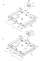
- FIG. 1 is a perspective view illustrating an organic EL panel according to a first embodiment of the present invention. It is a disassembled perspective view showing the organic electroluminescent panel of FIG. It is the disassembled perspective view which decomposed
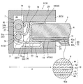
- FIG. 2 is an AA cross-sectional view showing a part of the organic EL panel of FIG. It is the perspective view seen from the back surface side of the board
- FIG. 3 is a side view of a second conductive member (lead-out side conductive member) in FIG. 2.
- FIG. 3 is an exploded perspective view in which a second conductive member (lead-out side conductive member) is removed from the inner frame member of FIG. 2.
- FIG. 3 is a perspective view illustrating a first conductive member (a power transmission conductive member) in FIG. 2. It is a disassembled perspective view showing the notch part vicinity of FIG.
- FIG. 15 is a schematic diagram showing a flow of current in the electric circuit of FIG. 14.
- the upper drawing is a cross-sectional view taken along the line AA of the organic EL panel in FIG. It is sectional drawing.
- FIG. 20 is an exploded perspective view showing the vicinity of the fixed frame part of FIG. 19.
- FIG. 20 is a CC cross-sectional view of the organic EL panel of FIG.
- FIG. 3 is an exploded perspective view of the organic EL device in FIG. 2.
- FIG. 33 is a sectional view taken along line AA in FIG. 32. It is sectional drawing in the state which mounted
- the organic EL panel 1 of the first embodiment is an organic EL panel mainly used as illumination.
- an organic EL device 2 a second conductive member (leading-side conductive member) 61, , A third conductive member (feeding portion contact side conductive member) 60, an inner frame member 5 (frame member), an outer frame member 6, and a first conductive member (power transmission conductive member) 7.
- the third conductive member (feeding portion contact-side conductive member) 60 and the second conductive member (lead-out side conductive member) 61 are collectively referred to as “the current-carrying member 3”.
- the organic EL device 2 of the present embodiment is obtained by laminating an organic EL element 10 on a substrate 8 (base material) having translucency as shown in FIG. 3 and actually emits light when driven in the plane. It has a light emitting region 11 and a plurality of power feeding regions 12 that are fed during driving. Specifically, the light emitting region 11 is located at the center in the longitudinal direction 1 of the organic EL device 2. The power feeding area 12 is arranged around the light emitting area 11 and on two sides of the light emitting area 11.
- the organic EL device 2 of the present embodiment is a so-called “bottom emission” type organic EL device that extracts light from at least the substrate 8 side.
- the organic EL device 2 includes one or a plurality of organic EL elements 10 in the light emitting region 11.
- the organic EL device 2 of the present embodiment employs a structure in which a plurality of organic EL elements 10 are built in correspondence with the light emitting region 11.
- a large number of organic EL elements 10 are planarly distributed on one surface of the substrate 8, and each organic EL element 10 is electrically connected in series on the substrate 8. That is, the organic EL device 2 used in the present embodiment is a so-called integrated organic EL device. Therefore, it is possible to reduce power loss due to a voltage drop between the electrode layers of the organic EL element 10. Moreover, the light emission uniformity within the surface of the light emitting region 11 can also be improved.
- a plurality of power feeding portions 15 are exposed on the side opposite to the substrate 8 (the third conductive member 60 side) as shown in FIG. More specifically, six power supply portions 15 are formed on the back side of the substrate 8 as shown in FIG. That is, power supply portions 15a, 15b, and 15c are provided at both ends and the center of one side. In addition, three power feeding portions 15a, 15b, and 15c are provided on opposite sides.
- the power feeding unit 15 is a portion where a conductive film 45 to be described later is exposed, and has an area of about several square millimeters to several square centimeters.
- the power feeding unit 15 is electrically connected to the first electrode layer 41 or the second electrode layer 43 in the organic EL element 10. In FIG.
- a portion where the power feeding unit 15 is electrically connected to the second electrode layer 43 is illustrated as in an enlarged view in a circle.
- the feeding portions 15 at the opposing positions are each connected to one of the first electrode layer 41 and the second electrode layer 43 in the organic EL element 10.
- the power feeding unit 15 electrically connected to the same electrode layer in the organic EL element 10 is provided in parallel.
- both power supply portions 15 a and 15 c located at one end of one side that is, at the end of one side in the longitudinal direction 1 of the substrate 8 are connected to the first electrode layer 41, they face each other.
- the power feeding units 15 a and 15 c located at opposite sides are also connected to the first electrode layer 41.
- the power feeding unit 15 (15b) located at the center of one side is connected to the second electrode layer 43
- the power feeding unit 15 (15b) located at the center of the opposite side is also connected to the second electrode layer 43. ing.
- the power feeding portions 15a, 15b, and 15a that are electrically connected to different electrode layers in the organic EL element 10 are alternately arranged.
- the power feeding unit 15 electrically connected to the first electrode layer 41 is also referred to as a power feeding unit 15a
- the power feeding unit electrically connected to the second electrode layer 43. 15 is also referred to as a power feeding unit 15b.
- the organic EL element 10 includes a functional layer 42 between at least the first electrode layer 41 and the second electrode layer 43 as shown in FIG. Further, in the organic EL element 10, a conductive film 45 (45a, 45b, 45c) electrically connected to the first electrode layer 41 or the second electrode layer 43 is laminated inside the organic EL element as shown in FIG. Yes.
- FIG. 22 is an exploded perspective view of a part of the organic EL element 10 in the organic EL device 2 of FIG.
- the conductive film 45 is an electrically conductive thin film that forms the power feeding unit 15.
- the conductive film 45 (45a, 45b, 45c) extends in the entire longitudinal direction l of the organic EL device 2.
- an insulating film 46 is laminated over the three conductive films 45a, 45b, and 45c in a region other than the power feeding unit 15.
- the power feeding portion 15 is a portion where the conductive film 45 as a conductive member is exposed.
- 4 is a portion where the conductive film 45 serving as the conductive member is exposed in the power feeding portion 15, and therefore the insulating film 46 does not exist.
- the power feeding units 15a and 15a, the power feeding units 15b and 15b, and the power feeding units 15a and 15a are electrically connected by the conductive films 45a, 45b, and 45c.
- the material of the first electrode layer 41 is not particularly limited.
- a metal such as indium tin oxide (ITO), indium zinc oxide (IZO), tin oxide (SnO 2 ), zinc oxide (ZnO), or the like.
- An oxide or a metal such as silver (Ag) or chromium (Cr) is employed.
- ITO or IZO which has high transparency, is particularly preferable in that light generated from the light emitting layer in the functional layer 42 can be effectively extracted. In this embodiment, ITO is adopted.
- the functional layer 42 is a layer provided between the first electrode layer 41 and the second electrode layer 43 and having at least one light emitting layer.
- the functional layer 42 is composed of a plurality of layers mainly made of an organic compound.
- the functional layer 42 can be formed of a known material such as a low molecular dye material or a conjugated polymer material used in a general organic EL device.
- the functional layer 42 may have a multilayer structure including a plurality of layers such as a hole injection layer, a hole transport layer, a light emitting layer, an electron transport layer, and an electron injection layer.
- the material of the second electrode layer 43 is not particularly limited, and examples thereof include silver (Ag) and aluminum (Al).
- the second electrode layer 43 of this embodiment is made of Al.
- the energization member 3 is formed of a third conductive member (feeding portion contact side conductive member) 60 and a second conductive member (leading side conductive member) 61, and the third conductive member (feeding portion contact).
- the side conductive member 60 and the second conductive member 61 (leading side conductive member) are separate bodies, they are in contact with each other and can be energized to each other.
- the third conductive member (feeding portion contact side conductive member) 60 is an abbreviation on the side opposite to the substrate 8 of the organic EL device 2 (the side facing the substrate 8 across the organic EL element 10) as shown in FIGS. It is a member that covers the entire surface.
- the third conductive member (feeding portion contact side conductive member) 60 is in the form of a sheet as shown in FIG. 6, and metal conductive foils 62 are embedded in resin in three rows in parallel.
- FIG. 6 is an explanatory diagram in which the conductive foil 62 of the third conductive member (feeding portion contact side conductive member) 60 is extended in a planar shape.
- the third conductive member 60 is formed by a plurality of conductive foils 62 and insulating resin films 63 a and 63 b that cover both the front and back surfaces of the conductive foil 62.
- the resin film 63 covers the three conductive foils 62 and intermediate portions of the conductive foils 62.
- the third conductive member (feeding portion contact side conductive member) 60 can conduct electricity through the conductive foil 62.
- the resin film 63 exists between the conductive foils 62, and the conductive foils 62 are insulated from each other by the resin film 63.
- the conductive foil 62 is a rectangular foil body as shown in FIG. 6, and the long side thereof is orthogonal to the longitudinal direction l of the organic EL device 2 (first conductive member (electrically conductive member for power transmission) 7). (Direction to do) is arranged along. Further, the respective conductive foils 62 are arranged in parallel with a predetermined interval in the width direction w, and are integrated by a resin film 63.
- the conductive foil 62 is not particularly limited as long as it is a conductive foil body. For example, a copper foil, a silver foil, a gold foil, a platinum foil, or the like can be employed. In the conductive foil 62 of this embodiment, a copper foil is used.
- the resin film 63 spreads in the direction w in which the conductive foils 62 are juxtaposed (the direction orthogonal to the longitudinal direction 1 of the conductive foil 62), and covers the three conductive foils 62a, 62b, and 62c.
- the third conductive member (feeding portion contact side conductive member) 60 the two resin films 63a and 63b are in close contact, and the conductive foil 62 is inserted between the resin films 63a and 63b.
- the resin film 63 is not particularly limited as long as it is an insulating resin thin film, and as a material, for example, a thin film such as polyethylene terephthalate (PET) or polyethylene (PE) can be adopted.
- PET polyethylene terephthalate
- PE polyethylene
- the third conductive member (feeding portion contact side conductive member) 60 includes an insulating region 65 in which the front and back surfaces of the conductive foil 62 are covered with the resin film 63 as shown in FIG.
- the conductive foil 62 is divided into an exposed conductive region 66.
- the conductive foil 62 of the conductive region 66 of the third conductive member (feeding portion contact side conductive member) 60 is bent and processed multiple times according to the side extending in the longitudinal direction l of the organic EL device 2 as shown in FIG. Has been.
- the conductive foil 62 of the conductive region 66 is bent twice so as to cover the end face of one side of the organic EL device 2 and has a “U” shape. That is, as shown in FIGS.
- the conductive foil 62 of the conductive region 66 is substantially flush with the insulating region 65 and faces the lower surface of the organic EL device 2 (the substrate 8 and the organic EL element 10 sandwiched therebetween).
- an end surface protection unit 68 that projects upward with respect to the lower surface protection unit 67 to protect the end surface of the organic EL device 2, and a projection of the end surface protection unit 68.
- An upper surface protection unit 69 that is folded back from the end in the direction l toward the organic EL device 2 side and protects the upper surface (substrate 8 side) of the organic EL device 2 is provided.
- the second conductive member (lead-out side conductive member) 61 bends one conductive plate having electrical conductivity. It is formed by processing, and has a continuous stepped cross-sectional shape as shown in FIGS. That is, the second conductive member (lead-out side conductive member) 61a is based on the state in which the organic EL panel 1 is assembled as shown in FIG.
- the first pressing portion 70, the energizing portion 71, and the second pressing portion 72 are provided toward the portion 21 side.
- the second conductive member (lead-out side conductive member) 61b is obtained by reversing the top of the second conductive member (lead-out side conductive member) 61a. Is described with reference to the second conductive member (lead-out side conductive member) 61a.
- the 1st press part 70 is a site
- the first pressing portion 70 is a standing wall portion 22 (FIG. 11) of the inner frame member 5 in the vicinity of the apex on the top surface portion 20 side of the inner frame member 5 as shown in FIGS.
- the first pressing portion 70 includes an organic EL side contact portion 73 that contacts the end surface protection portion 68 and a protection side contact portion 75 that contacts the protection member 50 of the first conductive member (power transmission conductive member) 7. Have. A predetermined space is formed between the organic EL side contact portion 73 and the protection side contact portion 75.
- the organic EL side contact portion 73 is inclined at a predetermined angle with respect to the top surface portion 20 of the inner frame member 5 as shown in FIG.
- the energization part 71 is a part that is in contact with and electrically connected to the first conductive member (conductive member for power transmission) 7.
- the energization part 71 is a portion curved in an arc shape, and the arc faces the outer frame member 6 side, and a part of the first conductive member (power transmission conductive member) 7 can be fitted inside.
- An arc portion 76 is provided. That is, the current-carrying unit 71 contacts a part of the first conductive member (power transmission conductive member) 7 with the arc part 76 as shown in FIG. It is possible to cover.
- the space inside the arc portion 76 is open in a direction inclined at a predetermined angle with respect to the bottom surface portion 26 of the outer frame member 6 as shown in FIG.
- the second pressing part 72 is a part that urges the third conductive member (power feeding part contact side conductive member) 60 in a direction approaching the power feeding part 15 of the organic EL device 2 by self-restoring force. That is, the 2nd press part 72 is a site
- the second pressing portion 72 includes an organic EL side contact portion 77 that contacts the lower surface protection portion 67 and a bottom surface side contact that contacts the bottom surface portion 26 of the outer frame member 6 when the organic EL panel 1 is assembled.
- a portion 78 is provided.
- a predetermined space is formed between the organic EL side contact portion 77 and the bottom surface side contact portion 78.
- the organic EL side contact portion 77 and the bottom surface side contact portion 78 are substantially parallel to each other.
- the inner frame member 5 is a member that can integrally hold the organic EL device 2 and the third conductive member (feeding portion contact side conductive member) 60 as shown in FIG. 4, and is a third conductive member for the organic EL device 2. (Feeding part contact side conductive member) A member that regulates the relative separation of 60.
- the third conductive member (power feeding unit contact side conductive member) 60 is pressed against the power feeding unit 15 of the organic EL device 2 by the inner frame member 5.
- the inner frame member 5 is a frame having a U-shaped cross section as shown in FIG. 8, and has a fixed space 17 into which at least one side of the organic EL device 2 can be inserted.
- the inner frame member 5 has a top surface portion 20, a bottom surface portion 21, and a standing wall portion 22 that connects the top surface portion 20 and the bottom surface portion 21, and the top surface portion 20, the bottom surface portion 21, and the standing wall portion 22. And a fixed space 17 surrounded by.
- the inner frame member 5 has a plurality of cutout portions communicating in the width direction w across the inner side (fixed space 17 side) and the outer side (outer frame member 6 side) of the inner frame member 5.
- 16 is formed.
- the inner frame member 5 includes a plurality of lower cutout portions 16 a cut out across the bottom surface portion 21 and the standing wall portion 22, and upper cutout portions cut out across the top surface portion 20 and the standing wall portion 22. It has a portion 16b. And the upper notch part 16b and the lower notch part 16a are alternately formed in the width direction w at predetermined intervals.
- the upper notch 16b is provided at the center in the width direction w, and two lower notches 16a are provided outside the upper notch 16b.
- interval between adjacent notch part 16a, 16b (16b, 16a) is the insulation area
- the notch widths of the notches 16a, 16b, and 16a are substantially equal to the widths of the corresponding exposed regions 52a, 52b, and 52a (see FIG. 9) of the first conductive member (conductive member for power transmission) 7. It has become.
- the length (height of the fixed space 17) H1 from the inner wall surface of the bottom surface portion 21 of the inner frame member 5 to the inner wall surface of the top surface portion 20 is substantially equal to the member thickness of the organic EL device 2 as shown in FIG. That is, the organic EL device 2 can be mounted inside the inner frame member 5.
- the length (height) H2 from the outer wall surface of the bottom surface portion 21 of the inner frame member 5 to the outer wall surface of the top surface portion 20 is the length from the inner wall surface of the bottom surface portion 26 of the outer frame member 6 to the inner wall surface of the top surface portion 25. Equal to height (height).
- the protruding length of the top surface portion 20 of the inner frame member 5 (length from the standing wall portion 22 to the end surface l in the protruding direction of the top surface portion 20) L1 is the protruding length of the bottom surface portion 21 of the inner frame member 5 (standing wall portion). 22 to the length in the protruding direction l of the bottom surface portion 21) and shorter than the length of the bottom surface portion 26 of the fixed frame portion 31 of the outer frame member 6. That is, the inner frame member 5 can be fitted inside the outer frame member 6.
- the outer frame member 6 constitutes the outline of the organic EL panel 1.
- the outer frame member 6 is a frame-shaped member that covers the outer peripheral edge of the organic EL device 2 as shown in FIG.
- the outer frame member 6 is formed of an “U” -shaped attachment frame portion 30 and a “I” -shaped fixed frame portion 31 in plan view.
- the attachment frame portion 30 is a frame having a substantially “U” cross-sectional shape, and is a member that covers the end faces of the three sides of the organic EL device 2.
- the attachment frame portion 30 can be attached along the edge of the organic EL device 2.
- the fixed frame portion 31 is a frame having a U-shaped cross section, and is a member that mainly covers the end face of the remaining one side of the organic EL device 2. That is, the fixed frame portion 31 has a top surface portion 25, a bottom surface portion 26, and a standing wall portion 27 that connects the top surface portion 25 and the bottom surface portion 26 as in the case of the inner frame member 5 as shown in FIG. 4.
- the end portion of the outer frame member 6 in the width direction w has a power supply hole 32 through which a part of the first conductive member (conductive member for power transmission) 7 can be inserted as shown in FIG.
- the opening shape of the power supply hole 32 has a shape along the outer shape of the first conductive member (conductive member for power transmission) 7.
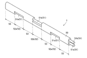
- the first conductive member (conductive member for power transmission) 7 is a linear body having an oval cross section as shown in FIG. 9, and a protective member 50 is covered around a plurality of long conductive wires 51. A plurality of conductive wires 51 are integrally formed by 50. That is, the first conductive member (conductive member for power transmission) 7 is a member that can conduct electricity through the conductive wire 51.
- the “oval shape” is a superordinate concept such as an egg shape, an oval shape, or an oval shape
- the first conductive member (conductive member for power transmission) 7 of the present embodiment has a rounded rectangular shape in cross section. It has a shape.
- the first conductive member (conductive member for power transmission) 7 has an exposed region 52 in which at least one (or one bundle) of the plurality of conductors 51 is exposed and the remaining conductors 51 are covered with the protective member 50. And an insulating region 53 whose periphery is covered with the protective member 50 with all the conductive wires 51. That is, at least one (or one bundle) of conductive wires 51 are exposed in the exposed region 52, and in the insulating region 53, the protective member 50 is covered with all of the conductive wires 51, and the internal conductive wire 51 is connected to the outside. It is electrically disconnected from (outside of the protective member 50).
- the two conductive wires 51 are each covered with a protective member 50, and the respective protective members 50 are integrally formed.
- the two conducting wires 51 are arranged in a line in the vertical direction (vertical direction). And the long axis of the section of the 1st conductive member (conductive member for power transmission) 7 has turned upside down.
- the exposed region 52 is an exposed region 52a in which only one conductor 51 (conductor 51a positioned downward in the vertical direction) is exposed, and an exposure in which only the other conductor 51 (conductor 51b positioned in the vertical direction) is exposed. Region 52b exists.
- the exposed regions 52a and the exposed regions 52b are alternately arranged at predetermined intervals in the width direction w.
- the first conductive member (conductive member for power transmission) 7 of this embodiment is arranged in the order of the exposed regions 52a, 52b, 52a in the width direction w.
- the protective member 50 located in the exposed region 52a has a substantially half-moon shape whose cross-sectional shape has an upward arc
- the protective member 50 located in the exposed region 52b has a substantially half-moon shape whose cross-sectional shape has a downward arc. It has become a shape.
- the longitudinal end w of the first conductive member (conductive member for power transmission) 7 protrudes to the outside of the outer frame member 6 as shown in FIG. Near the end in the longitudinal direction w of the first conductive member (power transmission conductive member) 7 and outside the outer frame member 6, all of the plurality of conducting wires 51 are exposed. That is, it is possible to supply electricity to the inside of the outer frame member 6 by attaching an external power source to the bare wire 51.
- the conducting wire 51 is not particularly limited as long as it is a linear body having electrical conductivity, and as a material, for example, a copper wire, a silver wire, a platinum wire, or the like can be adopted. Moreover, even if the conducting wire 51 is formed of one single wire, a plurality of single wires may be formed together.
- the protective member 50 is not particularly limited as long as it is an insulating resin film, and as a material, for example, insulating rubber or the like can be adopted.
- the outer frame member 6 covers the inner frame member 5 as shown in FIG. In other words, the inner frame member 5 is located inside the outer frame member 6. Most of the second conductive member (leading-side conductive member) 61 is housed in the notch 16 of the inner frame member 5 as shown in FIG. That is, in the organic EL panel 1, second conductive members (leading-side conductive members) 61 whose top and bottom are reversed in the width direction w are alternately arranged as shown in FIGS.
- the first pressing portion 70 is a positively-conducting second conductive member (leading-side conductive member) 61a positioned above the second pressing portion 72 in the vertical direction, and the second conductive A second conductive member (lead-out side conductive member) 61b obtained by reversing the top of the member (lead-out side conductive member) 61a, and a second conductive member (lead-out side conductive member) 61a in a normal posture are arranged.
- the standing wall portion 27 of the outer frame member 6 and the standing wall portion 22 of the inner frame member 5 are arranged at a predetermined interval as shown in FIG. 4, and the inner wall surface and the inner frame member of the standing wall portion 27 of the outer frame member 6 are arranged.
- a space 35 is formed between the five standing wall portions 22 and the outer wall surface. Further, most of the first conductive member (conductive member for power transmission) 7 is accommodated in the space 35.
- the space 35 extends in the width direction w, and the power feed hole 32 (see FIG. 2) of the outer frame member 6 is located on the extension of the extension direction w.
- the power supply hole 32 of the outer frame member 6 is inserted through the end of the first conductive member (power transmission conductive member) 7 in the longitudinal direction w, and the first conductive member (power transmission conductive member) 7 in the longitudinal direction.
- the end of w projects from the outer frame member 6.
- the projecting portion of the energization portion 71 is located in the exposed region 52 of the first conductive member (power transmission conductive member) 7 as shown in FIG. 10, and a conducting wire 51a is disposed therein. That is, a part of the arc portion 76 of the energization portion 71 is located in the exposed region 52 of the first conductive member (power transmission conductive member) 7, and the conductive wire 51 a is disposed therein. And the arc part 76 of the electricity supply part 71 is contacting the outer peripheral wall of the conducting wire 51a, and it has mutually engaged. Therefore, it is possible to energize between the conducting wire 51 a and the energization unit 71.
- the first conductive member (power transmission conductive member) 7 when viewed from the first conductive member (power transmission conductive member) 7 side, the first conductive member (power transmission conductive member) 7 is located at a position corresponding to the inside of the notch 16a as shown in FIGS.
- the exposed region 52a is located.
- the exposed region 52 of the first conductive member (conductive member for power transmission) 7 is located on the flat projection surface of the cutout portion 16a, which is a cutout of the standing wall portion 22 of the inner frame member 5. That is, at the position corresponding to the notch 16a, the conducting wire 51a is exposed as shown in FIG. 12, and the current-carrying part 71 of the second conductive member (leading-side conductive member) 61 is wound around the exposed part. In contact.
- the first pressing portion 70 of the second conductive member (leading-side conductive member) 61 is partially located in the exposed region 52a of the first conductive member (power transmission conductive member) 7 as shown in FIGS. It contacts the protective member 50a.
- the other part of the first pressing part 70 is in contact with the end face protection part 68 of the third conductive member (power feeding part contact side conductive member) 60.
- the protection-side contact portion 75 of the first pressing portion 70 is in contact with the protection member 50a
- the organic EL-side contact portion 73 of the first pressing portion 70 is the third conductive member (feeding portion contact).
- the side conductive member 60 is in contact with the end face protection portion 68.
- the 1st press part 70 is urging
- the first pressing part 70 presses the third conductive member (power feeding part contact side conductive member) 60 so as to be relatively close to the end face of the organic EL device 2.
- the second pressing portion 72 of the second conductive member (leading-side conductive member) 61 is housed in the notched portion 16a of the bottom surface portion 21 of the inner frame member 5 in a bent state as shown in FIGS. Moreover, the 2nd press part 72 is interposed between the bottom face part 26 of the outer frame member 6, and the lower surface protection part 67 of the 3rd electrically-conductive member (electric power feeding part contact side electrically-conductive member) 60 like FIG. Further, the bottom surface side contact portion 78 of the second pressing portion 72 is in contact with the bottom surface portion 26, and the organic EL side contact portion 77 of the second pressing portion 72 is in contact with the bottom surface protection portion 67.
- the second pressing portion 72 is biased in a direction in which the bottom surface portion 26 of the outer frame member 6 and the lower surface protection portion 67 of the third conductive member (feeding portion contact side conductive member) 60 are separated from each other. In other words, the second pressing portion 72 presses the third conductive member (feeding portion contact side conductive member) 60 relatively to the top surface portion 20 side of the inner frame member 5.
- the organic EL device 2 is pressed to the top surface portion 20 side of the inner frame member 5 through a third conductive member (feeding portion contact side conductive member) 60.
- a third conductive member (feeding portion contact side conductive member) 60 As shown in FIG. Further, the insulating region 65 of the third conductive member (feeding portion contact side conductive member) 60 covers at least the light emitting region 11. That is, the resin film 63 of the third conductive member (feeding portion contact side conductive member) 60 is positioned below the light emitting region 11 of the organic EL device 2 in the member thickness direction. Two sides facing the longitudinal direction 1 of the organic EL device 2 are covered with a conductive region 66 of a third conductive member (feeding portion contact side conductive member) 60. Specifically, as illustrated in FIG.
- the lower surface protection unit 67 is in surface contact with the power feeding unit 15 of the organic EL device 2
- the end surface protection unit 68 is in surface contact with the end surface of the organic EL device 2.
- the unit 69 is in surface contact with the upper surface of the organic EL device 2.
- the top surface portion 20 and the bottom surface portion 21 of the inner frame member 5 are covered from the outside in the vertical direction, and the inner frame member 5 includes the organic EL device 2 and the third conductive member (feeding portion contact side).
- Conductive member) 60 is sandwiched integrally.
- the lower surface protection part 67, the organic EL device 2, and the upper surface protection part 69 are interposed between the bottom surface part 21 and the top surface part 20 of the inner frame member 5 in this order from the bottom surface part 21 side. That is, the upper surface protection part 69 is sandwiched between the organic EL device 2 and the top surface part 20.
- the inner wall of the top surface portion 20 of the inner frame member 5 is pressed from the upper surface protection portion 69.
- the end face protection part 68 is pressed by the second conductive member (leading side conductive member) 61.
- the lower surface protection part 67 is pressed against the bottom surface part 21 of the inner frame member 5.
- the third conductive member (feeding portion contact side conductive member) 60 is pressed against the feeding portion 15 of the organic EL device 2 by the inner frame member 5.
- the third conductive member (feeding portion contact side conductive member) 60 is also pressed by the power feeding portion 15 of the organic EL device 2 by the second pressing portion 72 of the second conductive member (leading side conductive member) 61.
- the second conductive member (lead-out side conductive member) 61 and the third conductive member (feeding portion contact side conductive member) 60 are in contact with each other at two points, that is, the end surface protection portion 68 and the bottom surface protection portion 67. Further, as shown in FIG. 4, a part of the resin film 63 of the third conductive member (feeding portion contact side conductive member) 60 overlaps the inner frame member 5. That is, the exposed portion of the conductive foil 62 is contained in the inner frame member 5 and is not exposed to the outside of the inner frame member 5. Therefore, the outside of the organic EL panel 1 and the conductive foil 62 of the third conductive member (feeding portion contact side conductive member) 60 do not come into contact.
- the upper surface protection part 69 is pressed against the top surface part 20 of the inner frame member 5 around the notch part 16b cut out between the top surface part 20 and the standing wall part 22 of the inner frame member 5, and Except for being pressed by the second pressing portion 72 of the two conductive member (leading conductive member) 61, the structure around the notch portion 16a is substantially the same except that the structure is reversed upside down, and the description is redundant. Therefore, explanation is omitted.
- the second conductive member (lead-out conductive member) 61 that is a part of the energizing member 3 projects from the notch portion 16.
- a third conductive member (feeding portion contact-side conductive member) 60 that is a part of the energizing member 3 can be seen through the notch portion 16.
- the attachment frame part 30 is attached to three sides other than the side to which the fixed frame part 31 of the organic EL device 2 is attached, as shown in FIG. 13, and the fixed frame part 31 and the attachment frame are connected by a known fastening element. The part 30 is fastened.
- the inner frame member 5 is mounted in the fixed frame portion 31 of the outer frame member 6, and the first conductive member (conductive member for power transmission) 7 is placed in the space 35 positioned between the fixed frame portion 31 and the inner frame member 5.
- the second conductive member (lead-out side conductive member) 61 is attached in the notch 16, and the current-carrying portion 71 of the second conductive member (lead-out side conductive member) 61 is outside the inner frame member 5 and is the outer frame member. 6 is engaged with the first conductive member (conductive member for power transmission) 7.
- the second conductive member (lead-out side conductive member) 61 and the first conductive member (power transmission conductive member) 7 are engaged in the space 35.
- the third conductive member (feeding portion contact side conductive member) 60 is attached to the organic EL device 2 by a separate process. At this time, the conductive region 66 of the third conductive member (feeding portion contact side conductive member) 60 is bent along the edge of the organic EL device 2, and the third conductive member (feeding portion contact side conductive member) 60 and the organic EL device 2 are bent. And unite. Then, the organic EL device 2 and the conductive region 66 of the third conductive member (feeding portion contact side conductive member) 60 are integrally fitted into the attachment frame portion 30. That is, the attachment frame portion 30 is attached to the three sides of the organic EL device 2.
- the third conductive member (feeding portion contact side conductive member) 60 is regulated by the attachment frame portion 30.
- the third conductive member (power feeding unit contact side conductive member) 60 is pressed against the power feeding unit 15 of the organic EL device 2 by the inner frame member 5.
- the organic EL device 2 and the third conductive member (feeding portion contact side conductive member) 60 are integrally inserted into the inner frame member 5, and the fixed frame portion 31, the attachment frame portion 30, and the like. Is fixed by a known fastening element.
- the second conductive member (lead-out side conductive member) 61 is in a state in which the first pressing portion 70 is bent in the insertion direction 1 of the organic EL device 2, and the organic EL device 2 is separated from the inner frame member 5.
- the organic EL device 2 does not move away from the inner frame member 5, and the first pressing portion 70 presses the organic EL device 2.
- the second conductive member (lead-out side conductive member) 61 is in a state in which the second pressing portion 72 is bent in the vertical direction, and the organic EL device 2 and the third conductive member (feeding portion contact-side conductive member) 60 are disposed inside. Biasing is performed in a direction away from the bottom surface portion 21 of the frame member 5.
- the inner frame member 5 is an integral object, the organic EL device 2 and the third conductive member (feeding portion contact side conductive member) 60 are separated from the bottom surface portion 21 of the inner frame member 5 by the rigidity of the inner frame member 5.
- the organic EL device 2 and the third conductive member (feeding portion contact side conductive member) 60 are kept in close proximity and in contact with each other without being separated.
- the current flowing from the external power source passes through the conducting wire 51a of the first conductive member (power transmitting conductive member) 7 and reaches the energizing portion 71 of the second conductive member (lead-out side conductive member) 61 as shown in the upper diagram of FIG. . That is, the conducting wire 51a is connected to a positive pole of a power source (not shown). Further, the conducting wire 51b of the first conductive member (power transmitting conductive member) 7 is connected to a negative pole of a power source (not shown).
- the second conductive member (leading-side conductive member) 61 reaches the third conductive member (power-feeding portion contact-side conductive member) 60 via the second pressing portion 72 and the first pressing portion 70, and the power-feeding portion of the conductive region 66. It is transmitted from 15 a to the first electrode layer 41 of the organic EL device 2. Then, as shown in FIG. 16, the current spreads in a planar shape in the first electrode layer 41, travels through the organic EL device 2, and the functional layer 42 emits light. From the second electrode layer 43 through the power feeding unit 15 b, a third current flows. It is transmitted to the conductive region 66 of the conductive member (feeding portion contact side conductive member) 60. As shown in the lower diagram of FIG.
- the conductive region 66 of the third conductive member (feeding portion contact side conductive member) 60 passes through the first pressing portion 70 and the second pressing portion 72 of the second conductive member (leading side conductive member) 61.
- the electricity supply part 71 of the 2nd conductive member (leading-out side conductive member) 61 it leads to an external power supply via the conducting wire 51b of the 1st conductive member (conductive member for power transmission) 7.
- the second conductive member (lead-out side conductive member) 61 is provided between the first conductive member (conductive member for power transmission) 7 and the third conductive member (conductive portion contact-side conductive member) 60.
- the two conductive paths are provided.
- the first pressing portion 70 and the second pressing portion 72 of the second conductive member (leading-side conductive member) 61 is the first conductive member (power-transmitting conductive member) 7 or the third conductive member (feeding portion contact) Even if the contact with the side conductive member 60 is insufficient, the other functions as a conductive path, so that the current can be reliably supplied to the organic EL device 2.
- the power feeding unit 15 that is electrically connected to the same electrode layer is provided on the opposite side across the light emitting region 11, and a part of the power feeding unit 15 or Since the conductive region 66 of the third conductive member 60 (the power supply unit contact side conductive member) covers the power supply unit 15 so as to cover the whole, a current is generated in the functional layer in the organic EL device 2 as shown in FIG. Even if the organic EL panel 1 has a large area, it is difficult to produce a luminance distribution as a whole.
- the second conductive member (lead-out side conductive member) 61 is provided in the notch portion 16 of the inner frame member 5 in a state where the top and bottom are alternately reversed in the width direction w,
- the second pressing portion 72 of the second conductive member (leading-side conductive member) 61 presses the organic EL device 2 in the vertical direction.
- each second conductive member (leading side conductive member) 61 arranged in the width direction w is pressed toward the center side in the member thickness direction of the organic EL device 2, the organic EL The device 2 is unlikely to be detached from the inner frame member 5, and the contact between the power supply unit 15 and the third conductive member (power supply unit contact side conductive member) 60 can be maintained.
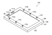
- the organic EL panel 100 of the second embodiment includes an organic EL device 102, a third conductive member (feeding portion contact side conductive member) 103, and a frame body 105 (frame member) as shown in FIGS. Yes.
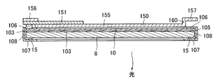
- the organic EL panel 100 includes a base member 150 including a mounting portion 151 that can be electrically connected to an external power source. It can be suitably attached to.
- the mounting portion 151 may have a circuit board including a rectifier circuit therein. Therefore, in the description of this embodiment, a case will be described in which a base member 150 that can be attached to a wall surface or the like is used as an instrument for fixing the organic EL panel 100.
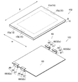
- the organic EL device 102 has substantially the same configuration as the organic EL device 2 of the first embodiment, but the number of power feeding units 15 is different. Specifically, the organic EL device 102 includes four power feeding units 15 (15a, 15a, 15b, 15b) as shown in FIG.
- the third conductive member (feeding portion contact side conductive member) 103 has substantially the same configuration as the third conductive member (feed portion contact side conductive member) 60 of the first embodiment, but the number of conductive foils 62 is the same. Is different. Specifically, the number of conductive foils 62 is determined in accordance with the number of power supply units 15 installed in the organic EL device 102. More specifically, in the third conductive member (feeding portion contact side conductive member) 103, the number of conductive foils 62 is half of the number of installed feeding portions 15 as shown in FIG. 27, and the two conductive foils 62a. , 62b. And the space
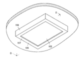
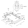
- the frame 105 is a frame-shaped member that covers the outer peripheral edge of the organic EL device 102 as shown in FIG.
- the frame 105 has a “B” shape in plan view, and is a frame having a substantially “U” cross-sectional shape as shown in FIG. That is, the frame body 105 is a member that covers the end faces of the four sides of the organic EL device 102 and can be mounted along the edge of the organic EL device 102.
- the material of the frame 105 is not particularly limited as long as it is a material having elasticity and flexibility. For example, silicone resin or rubber can be employed.
- the frame body 105 is preferably formed by integral molding.
- the size of the single frame 105 is slightly smaller than the size of the frame 105 when attached to the organic EL panel 100.
- the vertical, horizontal, or height of the frame 105 alone is 90% or more of the corresponding size among the vertical, horizontal, and height when attached to the organic EL panel 100. It is less than 100 percent, preferably 95 percent or more and 99 percent or less, and more preferably 96 percent or more and 98 percent or less.
- the frame 105 has a top surface portion 106, a bottom surface portion 107, and a standing wall portion 108 that connects the top surface portion 106 and the bottom surface portion 107.
- the fixed space 110 is surrounded by the standing wall 108.
- the top surface portion 106 has through holes 111a and 111b on one side (side extending in the width direction w).
- the through holes 111a and 111b have a rectangular opening shape, and are arranged in a line in the width direction w with a predetermined interval.
- the through holes 111a and 111b are the top surface portion 106, and the top and bottom of the conductive region 66 of the third conductive member (feeding portion contact side conductive member) 103 when the organic EL panel 100 is assembled as shown in FIG. Located on the direction projection plane.
- the through holes 111 a and 111 b are holes that penetrate the top surface portion 106 in the member thickness direction, and are continuous with the fixed space 110.
- two sides (sides extending in the longitudinal direction 1) of the top surface portion 106 sandwiching the one side having the through holes 111a and 111b each have one or a plurality of protrusions 112. .
- three protrusions 112 are arranged on each side in total, six in number.
- the protrusions 112 are arranged in a line in the longitudinal direction l at a predetermined interval.
- the protruding portion 112 has a first shaft portion 115, a second shaft portion 116, and a third shaft portion 117 from the base end side (the top surface portion 106 side) toward the distal end in the protruding direction. is doing.
- the first shaft portion 115, the second shaft portion 116, and the third shaft portion 117 are all cylindrical, and the respective central axes are on the same straight line. Further, the side surface of the first shaft portion 115 and the side surface of the second shaft portion 116, and the side surface of the second shaft portion 116 and the side surface of the third shaft portion 117 are respectively continuous in steps.
- the outer diameter L1 of the first shaft portion 115 is smaller than the outer diameter L2 of the second shaft portion 116 and is equal to the outer diameter L3 of the third shaft portion 117.
- the outer diameter L2 of the second shaft portion 116 is smaller than the maximum diameter R3 of the large diameter hole 163 of the fixing hole 161 of the base member 150 shown in FIG. 30 and larger than the maximum diameter R1 of the small diameter hole 162.
- the outer diameter L1 of the first shaft portion 115 is slightly smaller than the width R2 of the narrowed portion of the fixing hole 161 (the boundary portion between the large diameter hole 163 and the small diameter hole 162).
- the base member 150 is formed by a support member 154, a mounting portion 151, and connector portions 152 and 153.
- the support member 154 is formed of a main body portion 155, fixing portions 156 and 157, and connection portions 158 and 160 connecting the main body portion 155 and the fixing portions 156 and 157.
- the main body 155 protrudes with respect to the fixing portions 156 and 157.
- the main body 155 has a plurality of fixing holes 161 (161a to 161f) as shown in FIG.
- the opening shape of the fixing hole 161 is a shape in which two circles having different diameters intersect each other as shown in FIG. That is, the fixed hole 161 is a dharma hole having an opening shape like a bowl. More specifically, the fixing hole 161 is formed of a large diameter hole 163 and a small diameter hole 162. The fixing holes 161 are all directed in the same direction, and the large diameter hole 163 is located on the mounting portion 151 side (connector portions 152 and 153 side) with respect to the small diameter hole 162.
- the fixing holes 161 (161a, 161c, 161e, 161b, 161d, 161f) are arranged in a row near the side extending in the longitudinal direction l.
- the connecting portion 158 has a slit-shaped insertion hole 165 extending in the width direction w.
- the insertion hole 165 is a through hole into which a part of the mounting portion 151 described later can be inserted.
- the mounting unit 151 is mounted with known mounting components such as a direct current stabilized power supply, dimming, toning, and signal transmission / reception.
- the mounting portion 151 is electrically connected to the connector portions 152 and 153.
- the connector portions 152 and 153 are members that electrically connect the power feeding portions 15 a and 15 b of the organic EL device 102 in the organic EL panel 100 and the mounting portion 151 when the organic EL panel 100 is attached.
- the positional relationship of the base member 150 will be described. As shown in FIGS. 26 and 29, most of the mounting portion 151 is located on the main body portion 155, and the remaining portion is located below the fixed portion 156. Yes. That is, it extends over the main body 155 side and the fixed portion 156 side via the insertion hole 165 of the connection portion 158.
- the connector portions 152 and 153 are respectively connected to the mounting portion 151 located on the fixed portion 156 side, and the mounting portion 151 can supply power to the organic EL panel 100 from the connector portions 152 and 153.
- a third conductive member (feeding portion contact side conductive member) 103 is attached to and integrated with the organic EL device 102. Then, the frame body 105 is attached so as to cover the edges of the integrated organic EL device 102 and the third conductive member (feeding portion contact side conductive member) 103. Specifically, the elasticity and flexibility of the frame body 105 are used to expand (extend) the frame body 105 so as to be larger than the outer shape of the organic EL device 102, and the organic matter is fixed in the fixed space 110 of the frame body 105. The edge of the EL device 102 is fitted.
- the through holes 111a and 111b are attached so that the openings of the through holes 111a and 111b are located above the conductive region 66 of the third conductive member (feeding portion contact side conductive member) 103 as shown in FIG. That is, it is attached so that a part of the conductive region 66 of the third conductive member (feeding portion contact side conductive member) 103 is exposed from the openings of the through holes 111a and 111b.
- the lower surface protection portion 67 (see FIG. 26) of the third conductive member (feeding portion contact side conductive member) 103 is attached so as to be exposed from the openings of the through holes 111a and 111b.
- the lower surface protection portion 67 see FIG.
- the organic EL panel 100 prevents the third conductive member (feeding portion contact side conductive member) 103 from separating from the organic EL device 102. Further, since the organic EL panel 100 has the elastic and flexible frame 105 expanded and the organic EL device 102 is fitted therein, the organic EL device 102 is pressed by the restoring force of the frame 105. In addition, the frame 105 is unlikely to be detached from the organic EL device 102. In this embodiment as well, a part of the conductive region 66 of the third conductive member (feeding portion contact side conductive member) 103 can be seen through the openings of the through holes 111a and 111b of the frame 105.
- the protrusion 112 is inserted into the fixing hole 161 until the first shaft 115 (see FIG. 28) is positioned, and the organic EL panel 100 is slid in the longitudinal direction l.
- the first shaft portion 115 moves into the small-diameter hole 162 beyond the narrowed portion of the fixing hole 161 (the boundary portion between the large-diameter hole 163 and the small-diameter hole 162).
- the second shaft portion 116 is locked by the small-diameter hole 162 and prevents the organic EL panel 100 from separating from the base member 150 in the vertical direction. Further, the first shaft portion 115 is fitted in the small diameter hole 162.
- the second shaft portion 116 When viewed from the whole, the second shaft portion 116 is locked by the small-diameter hole 162 of the fixing hole 161, so that the connector portions 152 and 153 are connected to the conductive region 66 of the third conductive member (feeding portion contact side conductive member) 103. , 66 is kept pressed through the through holes 111a, 111b. That is, the connector parts 152 and 153 are electrically connected to the power feeding parts 15 a and 15 b of the organic EL device 102 via the third conductive member (power feeding part contact side conductive member) 103. Therefore, it is possible to reliably energize the organic EL device 102 from the outside.
- the second conductive member (lead-out side conductive member) 61 is electrically connected to the first conductive member (conductive member for power transmission) 7 via the notch portion 16 of the inner frame member 5.
- the present invention is not limited to this, and the notch 16 may be an opening.
- the conductive wire 51 is collectively arranged on one side of the organic EL panel.
- the present invention is not limited to this, and the position where the conductive wire 51 is folded is not particularly limited.
- the conductive wires 51 may be provided on two sides facing each other across the organic EL device 2.
- the lead wire 51 extends from the outer frame member 6 so that it can be electrically connected to an external power source.
- Power may be supplied from a middle portion of the outer frame member 6 by a connector or the like.
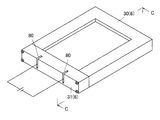
- a notch 80 is provided in the fixed frame portion 31 of the outer frame member 6, a connector 81 is inserted into the notch, and the lead wire 51 is electrically connected within the outer frame member 6.
- the protective member 50 is peeled off in accordance with the notch 80, so that the conducting wire 51 is exposed. .
- the organic EL panel 200 according to the third embodiment will be described.
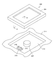
- 32 to 34 show an organic EL panel 200 according to the third embodiment.
- the organic EL panel 200 has a frame member 201 that covers four sides.
- An opening 203 is provided on the back side of the frame member 201 as shown in FIGS.
- An organic EL device 205 is attached to the frame member 201 as shown in FIGS.
- the layer configuration of the organic EL device 205 is substantially the same as that of the organic EL device 2 described above.
- the conductive region 66 of the third conductive member (feeding portion contact side conductive member) 60 covers the three surfaces of the substrate 8, whereas the organic EL of the present embodiment.
- the apparatus 205 only the back side of the substrate 8 is in surface contact as shown in FIGS.
- an iron plate 210 is mounted on the back side of the substrate 8 as shown in FIGS.
- a third conductive member (feeding portion contact side conductive member) 60 that is a part of the energizing member 3 can be seen through the opening 203 of the frame member 201.
- the organic EL device 205 of this embodiment is mounted on a base member 211 as shown in FIG.
- the base member 211 has a recess 212 into which the organic EL panel 200 fits, and a mounting portion 215 is provided in the recess 212.
- the mounting unit 215 may have a circuit board including a rectifier circuit therein.
- the mounting portion 215 is provided with contact pins 216.
- the contact pin 216 is a conductor that itself has elasticity.
- a magnet 220 is fixed to the base member 211.
- the organic EL device 205 is attached to the base member 211 by magnetic force.
- the contact pin 216 enters the opening 203 of the frame member 201 and comes into contact with the third conductive member (feeding portion contact side conductive member) 60 that is a part of the energizing member 3.
- the organic EL device 205 is attached to the base member 211 by the magnet 220 and is electrically connected.
- the organic EL device 205 and the base member 211 are integrated. However, it is attached to a mounting surface such as a wall by this magnetic force.
- the contact pin 216 (for example, a spring probe) is contracted through the opening 203 (for example, a notch portion) of the frame member 201 (for example, the frame).
- the third conductive member 60 which is a copper foil electrically connected to the base member 211, and the circuit board provided on the base member 211 are in electrical contact with high reliability, and power can be supplied from the outside.
- the contact pin 216 can also be provided on the third conductive member 60 side.
- a contact member having elasticity (for example, a coil connector manufactured by Yokoo Co., Ltd.) is attached so that the contact pin 216 can be accommodated in the opening 203, and the coil is magnetically attached. It is also a preferable form to conduct with the circuit board by shrinking.
- the frame member 201 presses the third conductive member (power feeding portion contact side conductive member) 60 against the power feeding portion 15 of the organic EL frame device 205.
- the third conductive member (power feeding unit contact side conductive member) 60 is also pressed by the power feeding unit 15 of the organic EL frame device 205 by the contact pin 216.
Landscapes
- Engineering & Computer Science (AREA)
- General Engineering & Computer Science (AREA)
- Electroluminescent Light Sources (AREA)
- Arrangement Of Elements, Cooling, Sealing, Or The Like Of Lighting Devices (AREA)
- Connecting Device With Holders (AREA)
Description
本発明は、主に照明として用いられる有機EL(Electro Luminescence)パネルに関するものである。
近年、白熱灯や蛍光灯に代わる照明装置として有機ELパネルが注目され、多くの研究がなされている。
ここで、有機ELパネルは、面状に広がりを持った有機EL装置にフレームなどの付属品を取り付けたものである。また、有機EL装置は、ガラス基板や透明樹脂フィルム、金属シート等の基材に、有機EL素子を積層し、この有機EL素子に給電するための給電構造を形成したものである。
そして、有機EL素子は、一方又は双方が透光性を有する2つの電極を対向させ、この電極の間に有機化合物からなる発光層を積層したものである。有機EL装置は、電気的に励起された電子と正孔との再結合のエネルギーによって発光する。
すなわち、有機ELパネルは自発光デバイスであり、発光層の材料を適宜選択することにより、種々の波長の光を発光することができる。
また、有機ELパネルは、白熱灯や蛍光灯、LED照明に比べて厚さが極めて小さくて軽量であり、且つ面状に発光するので、設置場所の制約が少ないという特長を有している。さらに、有機ELパネルは、白熱灯や蛍光灯に比べて発光効率が高いので消費電力が少なく、発熱が少ないという特長も有している。
そして、有機EL素子は、一方又は双方が透光性を有する2つの電極を対向させ、この電極の間に有機化合物からなる発光層を積層したものである。有機EL装置は、電気的に励起された電子と正孔との再結合のエネルギーによって発光する。
すなわち、有機ELパネルは自発光デバイスであり、発光層の材料を適宜選択することにより、種々の波長の光を発光することができる。
また、有機ELパネルは、白熱灯や蛍光灯、LED照明に比べて厚さが極めて小さくて軽量であり、且つ面状に発光するので、設置場所の制約が少ないという特長を有している。さらに、有機ELパネルは、白熱灯や蛍光灯に比べて発光効率が高いので消費電力が少なく、発熱が少ないという特長も有している。
ところで、白熱灯や蛍光灯、LED照明と同様に、有機ELパネルを発光させるためには、外部の電源から有機EL装置に給電し、上記した2つの電極間に電圧を印加する必要がある。すなわち、有機ELパネル外部の電源と、有機ELパネル内部の有機EL装置とを電気的に繋ぎ、有機EL装置に給電する給電構造が必要である。ところが、有機EL装置は、発光層として熱に弱い有機化合物を使用しているため、半田付けなどの高温で加熱する方法では、外部電源と電気的に接続された配線を有機EL装置内の電極に固着することができない。そのため、従来から、外部から有機EL装置に給電するための給電構造が模索されてきた(例えば、特許文献1)。
特許文献1の有機ELパネルでは、導電部材として電極に異方性導電膜(異方性導電フイルム)(ACF)を低温の熱で熱圧着させ、フレキシブル配線基板(FPC)に接続することで、外部電源と有機ELパネルを電気的に接続している。すなわち、ACFをFPCと電極との接着材として用い、FPCを介して外部電源から有機ELパネルに給電する方法が採用されている。
ところが、接着材としてACFを用いる場合でも、接着時に電極に対して、低温ではあるが熱を加える必要があるため、熱に弱い発光層に少なからず影響がある。そのため、有機EL装置の発光欠陥等の故障要因になるおそれがあった。また、接着材としてACFを用いると、半田等の接着手段に比べて高コストとなる。さらに接着材としてACFを用いると、電極との接触抵抗が大きくなる。そのため、有機ELパネルを発光させるためには過剰に電圧をかける必要が生じ、信頼性を低下させるという問題があった。そして、ACFとFPCと組み合わせる場合、有機ELパネルのサイズに合わせてFPCの形状等をその都度設計する必要があった。そのため、ACFとFPCを用いるとコストと手間がかかり、ACFとFPCの組み合わせに替わる給電構造の開発という市場からの要望があった。
ところが、接着材としてACFを用いる場合でも、接着時に電極に対して、低温ではあるが熱を加える必要があるため、熱に弱い発光層に少なからず影響がある。そのため、有機EL装置の発光欠陥等の故障要因になるおそれがあった。また、接着材としてACFを用いると、半田等の接着手段に比べて高コストとなる。さらに接着材としてACFを用いると、電極との接触抵抗が大きくなる。そのため、有機ELパネルを発光させるためには過剰に電圧をかける必要が生じ、信頼性を低下させるという問題があった。そして、ACFとFPCと組み合わせる場合、有機ELパネルのサイズに合わせてFPCの形状等をその都度設計する必要があった。そのため、ACFとFPCを用いるとコストと手間がかかり、ACFとFPCの組み合わせに替わる給電構造の開発という市場からの要望があった。
そこで、本発明は、有機ELパネルの外部から有機EL装置へ確実に給電できる有機ELパネルを提供することを課題とするものである。
上記課題を解決するための発明は、面状に広がりを有する基材に、2層の電極層と、前記電極層に挟まれた有機発光層が積層され、少なくとも一方の平面が発光面となる有機EL装置と、基材の少なくとも一辺を覆う枠部材を有する有機ELパネルにおいて、前記有機EL装置は、電極層に電気的に接続される給電部を有しており、前記枠部材は、開口又は切り欠きを有するものであり、電気伝導性を有した通電部材を有し、当該通電部材は、1又は複数の導電部材で構成されており、前記通電部材の一部は、有機EL装置側にあって前記給電部の一部又は全部を覆っており、枠部材は、通電部材を有機EL装置の給電部に押圧しており、前記通電部材の他の一部は、前記開口又は切り欠きを経由して枠部材の外側に張り出していることを特徴とする有機ELパネルである。
本発明の構成によれば、前記通電部材の他の一部は、前記開口又は切り欠きを経由して枠部材の外側に張り出している。言い換えると、通電部材の他の一部は、開口又は切り欠き内を挿通された状態となっており、枠部材の外側に通電部材の一部が露出している。
そのため、通電部材の露出部分に外部電源を接続させることで、有機ELパネルの外部から通電部材を介して有機EL装置に給電することが可能である。
さらに本発明の構成によれば、前記通電部材の一部は、有機EL装置側にあって前記給電部の一部又は全部を覆っており、枠部材は、通電部材を有機EL装置の給電部に押圧している。言い換えると、通電部材は、常時、枠部材によって有機EL装置の給電部に押しつけられており、給電部と接触している。そのため、常に有機EL装置の給電部と通電部材が接触した状態に維持でき、電気的に接続可能となっている。また、接触によって電気的に接続しているため、組み立て時に熱が発生せず、有機発光層に熱的な影響がない。
それ故に、有機ELパネルへの熱的な影響を防ぐとともに、有機ELパネルの外部から有機EL装置へ確実に給電することができる。
そのため、通電部材の露出部分に外部電源を接続させることで、有機ELパネルの外部から通電部材を介して有機EL装置に給電することが可能である。
さらに本発明の構成によれば、前記通電部材の一部は、有機EL装置側にあって前記給電部の一部又は全部を覆っており、枠部材は、通電部材を有機EL装置の給電部に押圧している。言い換えると、通電部材は、常時、枠部材によって有機EL装置の給電部に押しつけられており、給電部と接触している。そのため、常に有機EL装置の給電部と通電部材が接触した状態に維持でき、電気的に接続可能となっている。また、接触によって電気的に接続しているため、組み立て時に熱が発生せず、有機発光層に熱的な影響がない。
それ故に、有機ELパネルへの熱的な影響を防ぐとともに、有機ELパネルの外部から有機EL装置へ確実に給電することができる。
また同様の課題を解決するもう一つの発明は、面状に広がりを有する基材に、2層の電極層と、前記電極層に挟まれた有機発光層が積層され、少なくとも一方の平面が発光面となる有機EL装置と、基材の少なくとも一辺を覆う枠部材を有する有機ELパネルにおいて、前記有機EL装置は、前記電極層に電気的に接続された給電部を有しており、前記枠部材は、開口又は切り欠きを有するものであり、電気伝導性を有した1又は複数の導電部材で構成された通電部材を有し、前記通電部材の一部は、前記給電部の一部又は全部を覆っており、枠部材は、前記通電部材を有機EL装置の給電部に押圧しており、前記通電部材の他の一部は、前記開口又は切り欠きから露出していることを特徴とする有機ELパネルである。
同様の課題を解決するさらにもう一つの発明は、面状に広がりを有する基材に、2層の電極層と、前記電極層に挟まれた有機発光層が積層され、少なくとも一方の平面が発光面となる有機EL装置と、基材の少なくとも一辺を覆う枠部材を有する有機ELパネルにおいて、前記有機EL装置は、前記電極層に電気的に接続された給電部を有しており、前記枠部材は、開口又は切り欠きを有するものであり、電気伝導性を有した通電部材を有し、当該通電部材は、平面的な広がりを有する金属露出部を有し、給電部についても平面的な広がりを有する導電部材露出部を有し、前記給電部に通電部材が押圧された状態で面接触していると共に、前記通電部材の一部が前記開口又は切り欠きから覗き見える状態であることを特徴とする有機ELパネルである。
前記した有機ELパネルは、枠部材の外側を覆う外枠部材と、外部電源と電気的に接続可能な第1導電部材を有し、当該外枠部材と前記枠部材の間には、所定の空間が形成されており、前記第1導電部材は、当該空間に配されるものであって、当該空間の延伸方向に延在しており、前記通電部材の一部は、当該空間内に進入し、第1導電部材と接触していることが望ましい。
ここで第1導電部材は、外部の電源に接続されて有機EL装置に送電する部材である。従って、前記した発明は、枠部材の外側を覆う外枠部材と、外部電源と電気的に接続可能な送電用導電部材を有し、当該外枠部材と前記枠部材の間には、所定の空間が形成されており、前記送電用導電部材は、当該空間に配されるものであって、当該空間の延伸方向に延在しており、前記通電部材の一部は、当該空間内に進入し、送電用導電部材と接触していること構造である。
本発明の構成によれば、外枠部材と枠部材の間には、所定の空間が形成されている。すなわち、枠部材の配された部位では、外枠部材と枠部材との2重構造を形成しており、外枠部材と枠部材の間に隙間がある。
そして、本発明の構成によれば、外枠部材は、枠部材の外側を覆っているため、当該空間(隙間)内に配された第1導電部材(送電用導電部材)は、外枠部材によって外部から隠され、外部から視認不能又は視認困難となっている。そのため、本発明の有機ELパネルは見栄えがよい。
そして、本発明の構成によれば、外枠部材は、枠部材の外側を覆っているため、当該空間(隙間)内に配された第1導電部材(送電用導電部材)は、外枠部材によって外部から隠され、外部から視認不能又は視認困難となっている。そのため、本発明の有機ELパネルは見栄えがよい。
通電部材は、給電部と接する給電部接触側導電部材と、当該給電部接触側導電部材と接触する導出側導電部材とを有するものであってもよい。
また前記通電部材は、給電部と直接接触する箔状の第3導電部材と、当該第3導電部材と接触し前記開口又は切り欠きを経由して枠部材の外側に張り出した第2導電部材を有し、第2導電部材は、第3導電部材を給電部に押圧するように付勢する押圧部を有しているものであってもよい。
ここで、第3導電部材は、有機EL装置の給電部と接するものであり、給電部接触側導電部材に相当する。また第2導電部材は、導出側導電部材に相当する。
従って、前記した発明は、前記通電部材は、給電部と直接接触する箔状の給電部接触側導電部材と、当該給電部接触側と接触し前記開口又は切り欠きを経由して枠部材の外側に張り出した導出側導電部材を有し、導出側導電部材は、給電部接触側導電部材を給電部に押圧する押圧部を有した構成の有機ELパネルである。
従って、前記した発明は、前記通電部材は、給電部と直接接触する箔状の給電部接触側導電部材と、当該給電部接触側と接触し前記開口又は切り欠きを経由して枠部材の外側に張り出した導出側導電部材を有し、導出側導電部材は、給電部接触側導電部材を給電部に押圧する押圧部を有した構成の有機ELパネルである。
本発明の構成によれば、第2導電部材(導出側導電部材)は、第3導電部材(給電部接触側導電部材)を給電部に押圧するように付勢する押圧部を有している。すなわち、第2導電部材(導出側導電部材)によっても、第3導電部材(給電部接触側導電部材)は有機EL装置の給電部に押しつけられている。そのため、より確実に有機EL装置の給電部に通電部材(第3導電部材)の一部を接触させることが可能であり、接触抵抗をさらに低減することができる。
前記した通電部材は、給電部と接する給電部接触側導電部材を有し、当該給電部接触側導電部材は互いに絶縁状態にある複数系統の通電系統を有するものであってもよい。
前記した通電部材は、給電部と接する給電部接触側導電部材と、当該給電部接触側導電部材と接触する導出側導電部材とを有し、導出側導電部材は互いに絶縁状態にある複数系統の通電系統を有するものであってもよい。
通電部材の一つは、複数の導電箔が平面的に配置され、前記複数の導電箔の表裏両面に絶縁性の樹脂が設けられたものであってもよい。
1以上の導電箔が有機EL装置の前記2層の電極層の一方に電気的に接続され、他の1以上の導電箔が有機EL装置の前記2層の電極層の他方に電気的に接続されていてもよい。
通電部材の一つは、金属箔の表裏両面に絶縁性の樹脂が設けられて成るシート状の部材であり、端部に前記金属箔が露出し、当該露出部分が給電部と接していてもよい。
通電部材の一つは、金属箔の表裏両面に絶縁性の樹脂が設けられて成るシート状の部材であり、端部に前記金属箔の表裏面が露出し、当該露出部分の一方の面が給電部と接し、他方の面が他の導電部材と接していてもよい。
通電部材の少なくとも一つは、平面的な広がりを有する金属露出部を有し、給電部についても平面的な広がりを有する導電部材露出部を有し、前記給電部に通電部材が面接触していてもよい。
通電部材は、給電部と接する給電部接触側導電部材と、当該給電部接触側導電部材と接触する導出側導電部材とを有し、導出側導電部材によっても給電部接触側導電部材が給電部に押圧されていてもよい。
導出側導電部材は、自己の持つ弾性によって給電部接触側導電部材を給電部に押圧するものであってもよい。
導出側導電部材を給電部接触側導電部材に付勢する付勢部材を有し、当該付勢部材によって導出側導電部材が電部接触側導電部材を給電部に押圧されていてもよい。
通電部材の一部が枠部材の前記開口又は切り欠きから張り出し、当該張り出し方向は、基材の表面方向又は裏面方向であってもよい。
通電部材の一部が枠部材の前記開口又は切り欠きから張り出し、当該張り出し方向は、基材の端面方向であってもよい。
外部電源と電気的に接続可能な送電用導電部材を有し、送電用導電部材は、電源のプラス極に接続されるプラス側導体と、電源のマイナス極に接続されるマイナス側導体を有するものであってもよい。
外部電源と電気的に接続可能な送電用導電部材と、有機ELパネルの外郭を構成する外枠部材を有し、基材の少なくとも一辺と、外枠部材の内周面との間に前記送電部材が配され、当該送電部材から通電部材を経て前記給電部に給電されるものであってもよい。
外部電源と電気的に接続可能な送電用導電部材を有し、前記送電部材は、一部又は全部が露出した長尺状の金属であってもよい。
給電部は、基材の表裏面の少なくとも一方であって、基材の辺の近傍に露出しているものであってもよい。
給電部は、基材の表裏面の少なくとも一方であって、基材の辺の近傍に露出しており、通電部材の一つは、露出した金属箔を有し、当該金属箔が基材の表面と、端面と、裏面の3面を覆っていてもよい。
給電部は、基材の表裏面の少なくとも一方であって、基材の対向する2辺の近傍に露出しており、通電部材の一つは、金属箔の表裏面に絶縁性の樹脂が設けられて成るシート状の部材であり、両端部に前記金属箔が露出し、当該露出部分が給電部と接していてもよい。
給電部は、基材の一辺とこれに対向する辺にあり、枠部材は、少なくとも前記2辺を覆うものであってもよい。
枠部材は、基材の辺の近傍の表面と、端面と、裏面の3面を覆う凹溝を有し、前記凹溝内に、基材と通電部材が挟まれて通電部材を基材の給電部に押圧しているものであってもよい。
整流回路を含む回路基板を有していてもよい。
磁力によって他の部材に取り付け可能であってもよい。
本発明の構成によれば、外部から有機ELパネル内の有機EL装置に確実に給電できる。
以下、本発明の実施形態について詳細に説明する。
なお、以下の説明において、特に断りがない限り、有機ELパネル1の上下左右の位置関係は、図1の姿勢を基準に説明する。
なお、以下の説明において、特に断りがない限り、有機ELパネル1の上下左右の位置関係は、図1の姿勢を基準に説明する。
第1実施形態の有機ELパネル1は、主に照明として使用される有機ELパネルであり、図1~図3のように有機EL装置2と、第2導電部材(導出側導電部材)61と、第3導電部材(給電部接触側導電部材)60と、内枠部材5(枠部材)と、外枠部材6と、第1導電部材(送電用導電部材)7とを備えている。なお本実施形態では、第3導電部材(給電部接触側導電部材)60と、第2導電部材(導出側導電部材)61をまとめて「通電部材3」と称している。
以下、有機ELパネル1を形成する各部材の構成について説明する。
本実施形態の有機EL装置2は、図3のように透光性を有した基板8(基材)に有機EL素子10を積層したものであり、その面内において、駆動時に実際に発光する発光領域11と、駆動時に給電される複数の給電領域12を有している。具体的には、発光領域11は、有機EL装置2の長手方向lの中央に位置している。給電領域12は、発光領域11の周囲であって、発光領域11を挟んだ2辺側にそれぞれ配されている。また、本実施形態の有機EL装置2は、少なくとも基板8側から光を取り出す、いわゆる「ボトムエミッション」型の有機EL装置である。
本実施形態の有機EL装置2は、図3のように透光性を有した基板8(基材)に有機EL素子10を積層したものであり、その面内において、駆動時に実際に発光する発光領域11と、駆動時に給電される複数の給電領域12を有している。具体的には、発光領域11は、有機EL装置2の長手方向lの中央に位置している。給電領域12は、発光領域11の周囲であって、発光領域11を挟んだ2辺側にそれぞれ配されている。また、本実施形態の有機EL装置2は、少なくとも基板8側から光を取り出す、いわゆる「ボトムエミッション」型の有機EL装置である。
有機EL装置2には、発光領域11に1又は複数の有機EL素子10が内蔵されている。本実施形態の有機EL装置2は、発光領域11に対応して複数の有機EL素子10が内蔵された構造が採用されている。本実施形態では、多数の有機EL素子10が基板8の一面に平面的に分布しており、各有機EL素子10が基板8上で電気的に直列に接続されている。すなわち、本実施形態で使用する有機EL装置2は、いわゆる集積型の有機EL装置である。そのため、有機EL素子10の電極層間の電圧降下による電力ロスを低減することが可能である。また、発光領域11面内の発光均一性を高めることもできる。
給電領域12においては、図3のように基板8と反対側(第3導電部材60側)に複数の給電部15が露出している。より具体的には、図6の様に基板8の裏面側に給電部15が6個形成されている。即ち一つの辺の両端と中央に給電部15a,15b,15cが設けられている。また対向する辺にも3個の給電部15a,15b,15cが設けられている。
給電部15は、後記する導電膜45が露出した部分であり、数平方ミリから数平方センチ程度の面積を有している。
給電部15は、有機EL素子10内の第1電極層41又は第2電極層43に電気的に接続されている。図4では、円内の拡大図の様に、給電部15が第2電極層43に電気的に接続された部分を図示している。
対向する位置にある給電部15は、それぞれ有機EL素子10内の第1電極層41又は第2電極層43の内の一方に接続されている。言い換えると、内枠部材5の取り付け時における基板8の挿入方向lにおいては、有機EL素子10内の同一電極層と電気的に接続された給電部15が並設されている。
本実施形態では、一つの辺の両端部すなわち、基板8の長手方向lにおいて、一方の辺の端部に位置する給電部15a,15cが第1電極層41と接続されていると、対向する辺の対向する位置にある給電部15a,15cも第1電極層41と接続されている。
また一方辺の中央に位置する給電部15(15b)が第2電極層43と接続されていると、対向する辺の中央に位置する給電部15(15b)も第2電極層43と接続されている。
給電部15は、後記する導電膜45が露出した部分であり、数平方ミリから数平方センチ程度の面積を有している。
給電部15は、有機EL素子10内の第1電極層41又は第2電極層43に電気的に接続されている。図4では、円内の拡大図の様に、給電部15が第2電極層43に電気的に接続された部分を図示している。
対向する位置にある給電部15は、それぞれ有機EL素子10内の第1電極層41又は第2電極層43の内の一方に接続されている。言い換えると、内枠部材5の取り付け時における基板8の挿入方向lにおいては、有機EL素子10内の同一電極層と電気的に接続された給電部15が並設されている。
本実施形態では、一つの辺の両端部すなわち、基板8の長手方向lにおいて、一方の辺の端部に位置する給電部15a,15cが第1電極層41と接続されていると、対向する辺の対向する位置にある給電部15a,15cも第1電極層41と接続されている。
また一方辺の中央に位置する給電部15(15b)が第2電極層43と接続されていると、対向する辺の中央に位置する給電部15(15b)も第2電極層43と接続されている。
言い換えると、基板8の幅方向wにおいては、有機EL素子10内の異なる電極層と電気的に接続された給電部15a,15b,15aが交互に並んでいる。
なお、以下の説明において、理解を容易にするため、第1電極層41と電気的に接続された給電部15を給電部15aともいい、第2電極層43と電気的に接続された給電部15を給電部15bともいう。
なお、以下の説明において、理解を容易にするため、第1電極層41と電気的に接続された給電部15を給電部15aともいい、第2電極層43と電気的に接続された給電部15を給電部15bともいう。
また、有機EL素子10は、図4のように少なくとも第1電極層41と第2電極層43との間に機能層42を備えたものである。さらに、有機EL素子10は図22のように第1電極層41又は第2電極層43に電気的に接続された導電膜45(45a,45b,45c)が有機EL素子の内部に積層されている。なお、図22は、図3の有機EL装置2について有機EL素子10の一部を分解した斜視図である。導電膜45は給電部15を形成する電気伝導性を有した薄膜である。導電膜45(45a,45b,45c)は有機EL装置2の長手方向l全体に延びている。また、給電部15以外の領域には、3枚の導電膜45a,45b,45cに亘って絶縁膜46が積層している。逆に言えば、給電部15は導電部材たる導電膜45が露出した部分である。
なお図4の円内は、給電部15であって導電部材たる導電膜45が露出する部分であるから、絶縁膜46は存在しない。
有機EL装置2では、導電膜45a,45b,45cによって、給電部15a,15a、給電部15b,15b、給電部15a,15a間を電気的に接続している。
なお図4の円内は、給電部15であって導電部材たる導電膜45が露出する部分であるから、絶縁膜46は存在しない。
有機EL装置2では、導電膜45a,45b,45cによって、給電部15a,15a、給電部15b,15b、給電部15a,15a間を電気的に接続している。
第1電極層41の素材は、特に限定されるものではなく、例えば、インジウム錫酸化物(ITO)、インジウム亜鉛酸化物(IZO)、酸化錫(SnO2 )、酸化亜鉛(ZnO)等の金属酸化物や、銀(Ag)、クロム(Cr)等のような金属などが採用される。機能層42内の発光層から発生した光を効果的に取り出せる点では、透明性が高いITOあるいはIZOが特に好ましい。本実施形態では、ITOを採用している。
機能層42は、第1電極層41と第2電極層43との間に設けられ、少なくとも一つの発光層を有している層である。機能層42は、主に有機化合物からなる複数の層から構成されている。この機能層42は、一般的な有機EL装置に用いられている低分子系色素材料や、共役系高分子材料などの公知のもので形成することができる。また、この機能層42は、ホール注入層、ホール輸送層、発光層、電子輸送層、電子注入層などの複数の層からなる積層多層構造であってもよい。
第2電極層43の素材は、特に限定されるものではなく、例えば銀(Ag)やアルミニウム(Al)などが挙げられる。本実施形態の第2電極層43は、Alで形成されている。
続いて、通電部材3について説明する。
通電部材3は、図4のように第3導電部材(給電部接触側導電部材)60と、第2導電部材(導出側導電部材)61から形成されており、第3導電部材(給電部接触側導電部材)60と第2導電部材(導出側導電部材)61は別体であるが、両者は接触して相互に通電可能となっている。
第3導電部材(給電部接触側導電部材)60は、図5,図6のように有機EL装置2の基板8と反対側(有機EL素子10を挟んで基板8と対向する側)の略全面を覆う部材である。
第3導電部材(給電部接触側導電部材)60は図6の様にシート状であり、樹脂の中に金属製の導電箔62が3列平行に埋設されたものである。
図6は、第3導電部材(給電部接触側導電部材)60の導電箔62を平面状に引き延ばした説明図である。
第3導電部材60は、図6のように複数の導電箔62と、導電箔62の表裏の両面を覆った絶縁性の樹脂膜63a,63bとによって、形成されている。本実施形態では、3枚の導電箔62と、その導電箔62のそれぞれの中間部を樹脂膜63が覆っている。すなわち、第3導電部材(給電部接触側導電部材)60は、導電箔62を介して電気伝導が可能となっている。各導電箔62同士の間には前記した様に樹脂膜63が存在し、樹脂膜63によって各導電箔62同士が絶縁されている。
通電部材3は、図4のように第3導電部材(給電部接触側導電部材)60と、第2導電部材(導出側導電部材)61から形成されており、第3導電部材(給電部接触側導電部材)60と第2導電部材(導出側導電部材)61は別体であるが、両者は接触して相互に通電可能となっている。
第3導電部材(給電部接触側導電部材)60は、図5,図6のように有機EL装置2の基板8と反対側(有機EL素子10を挟んで基板8と対向する側)の略全面を覆う部材である。
第3導電部材(給電部接触側導電部材)60は図6の様にシート状であり、樹脂の中に金属製の導電箔62が3列平行に埋設されたものである。
図6は、第3導電部材(給電部接触側導電部材)60の導電箔62を平面状に引き延ばした説明図である。
第3導電部材60は、図6のように複数の導電箔62と、導電箔62の表裏の両面を覆った絶縁性の樹脂膜63a,63bとによって、形成されている。本実施形態では、3枚の導電箔62と、その導電箔62のそれぞれの中間部を樹脂膜63が覆っている。すなわち、第3導電部材(給電部接触側導電部材)60は、導電箔62を介して電気伝導が可能となっている。各導電箔62同士の間には前記した様に樹脂膜63が存在し、樹脂膜63によって各導電箔62同士が絶縁されている。
導電箔62は、図6のように長方形状の箔体であり、その長辺が有機EL装置2の長手方向l(第1導電部材(送電用導電部材)7の延伸方向wに対して直交する方向)に沿うように配置されている。また、それぞれの導電箔62は、幅方向wに所定の間隔を空けて平行に配されており、樹脂膜63によって一体化されている。
導電箔62は、導電性を有した箔体であれば特に限定されるものではなく、例えば、銅箔や銀箔、金箔、白金箔などが採用できる。なお、本実施形態の導電箔62では、銅箔を用いている。
導電箔62は、導電性を有した箔体であれば特に限定されるものではなく、例えば、銅箔や銀箔、金箔、白金箔などが採用できる。なお、本実施形態の導電箔62では、銅箔を用いている。
樹脂膜63は、導電箔62の並設方向w(導電箔62の長手方向lに対して直交する方向)に広がっており、3枚の導電箔62a,62b,62cに亘って覆う。第3導電部材(給電部接触側導電部材)60は、2枚の樹脂膜63a,63bが密着しており、樹脂膜63a,63bの間に導電箔62が挿通された状態となっている。
樹脂膜63は、絶縁性を有した樹脂薄膜であれば特に限定されるものではなく、素材としては、例えば、ポリエチレンテレフタレート(PET)、ポリエチレン(PE)などの薄膜が採用できる。
樹脂膜63は、絶縁性を有した樹脂薄膜であれば特に限定されるものではなく、素材としては、例えば、ポリエチレンテレフタレート(PET)、ポリエチレン(PE)などの薄膜が採用できる。
また、第3導電部材(給電部接触側導電部材)60は、図6のように導電箔62の表裏両面を樹脂膜63が覆った絶縁領域65と、絶縁領域65の長手方向lの両外側であって、導電箔62が露出した導電領域66とに分けられる。
また、第3導電部材(給電部接触側導電部材)60の導電領域66の導電箔62は、図3のように有機EL装置2の長手方向lに延びる辺に合わせて、複数回折り曲げて加工されている。具体的には、導電領域66の導電箔62は、有機EL装置2の一辺の端面を覆うように2回折り曲げられ「コ」の字状になっている。
すなわち、導電領域66の導電箔62は、図3,図4のように、絶縁領域65と略同一平面上であって、有機EL装置2の下面(基板8と有機EL素子10を挟んで対向する側)に配された下面保護部67(図4)と、下面保護部67に対して上方に向けて突出し有機EL装置2の端面を保護する端面保護部68と、端面保護部68の突出方向l端部から有機EL装置2側に折り返され有機EL装置2の上面(基板8側)を保護する上面保護部69を有している。
また、第3導電部材(給電部接触側導電部材)60の導電領域66の導電箔62は、図3のように有機EL装置2の長手方向lに延びる辺に合わせて、複数回折り曲げて加工されている。具体的には、導電領域66の導電箔62は、有機EL装置2の一辺の端面を覆うように2回折り曲げられ「コ」の字状になっている。
すなわち、導電領域66の導電箔62は、図3,図4のように、絶縁領域65と略同一平面上であって、有機EL装置2の下面(基板8と有機EL素子10を挟んで対向する側)に配された下面保護部67(図4)と、下面保護部67に対して上方に向けて突出し有機EL装置2の端面を保護する端面保護部68と、端面保護部68の突出方向l端部から有機EL装置2側に折り返され有機EL装置2の上面(基板8側)を保護する上面保護部69を有している。
第2導電部材(導出側導電部材)61に目を移すと、第2導電部材(導出側導電部材)61(61a,61b,61a)は、電気伝導性を有した1枚の導電板を折り曲げ加工することによって形成されており、図7,図8に示すように、連続した段状の断面形状を有している。すなわち、第2導電部材(導出側導電部材)61aは、図7のように有機ELパネル1を組み立てた状態を基準に、内枠部材5の天地方向上方(天面部20側)から下方(底面部21側)に向けて、第1押圧部70と、通電部71と、第2押圧部72とを有している。なお、第2導電部材(導出側導電部材)61bは、第2導電部材(導出側導電部材)61aの天地を逆転したものであるため、第2導電部材(導出側導電部材)61の各部位の説明については、第2導電部材(導出側導電部材)61aを基準に説明する。
第1押圧部70は、自己復元力によって有機EL装置2の端面を内枠部材5から離反する方向に付勢する部位である。すなわち、第1押圧部70は、図4のように後述する第1導電部材(送電用導電部材)7と有機EL装置2の端面との間に介在する部位であり、弾性によって、長手方向l中央側に有機EL装置2の端面を付勢することができる。
第1押圧部70は、有機ELパネル1を組み立てた際に、図4,図7のように内枠部材5の天面部20側の頂点近傍において内枠部材5の立壁部22(図11)側に円弧状に折り返されている。また、第1押圧部70は、端面保護部68に当接する有機EL側当接部73と、第1導電部材(送電用導電部材)7の保護部材50と当接する保護側当接部75を有している。有機EL側当接部73と保護側当接部75との間には、所定の空間が形成されている。有機EL側当接部73は、図4のように内枠部材5の天面部20に対して所定の角度で傾斜している。
第1押圧部70は、有機ELパネル1を組み立てた際に、図4,図7のように内枠部材5の天面部20側の頂点近傍において内枠部材5の立壁部22(図11)側に円弧状に折り返されている。また、第1押圧部70は、端面保護部68に当接する有機EL側当接部73と、第1導電部材(送電用導電部材)7の保護部材50と当接する保護側当接部75を有している。有機EL側当接部73と保護側当接部75との間には、所定の空間が形成されている。有機EL側当接部73は、図4のように内枠部材5の天面部20に対して所定の角度で傾斜している。
通電部71は、第1導電部材(送電用導電部材)7と接触し電気的に接続される部位である。通電部71は、円弧状に湾曲した部位であり、その弧は外枠部材6側を向いており、内側に第1導電部材(送電用導電部材)7の一部を嵌め込むことが可能な弧部76を有している。すなわち、通電部71は、図4のように弧部76で第1導電部材(送電用導電部材)7の一部に接触しながら、第1導電部材(送電用導電部材)7の一部を覆うことが可能となっている。弧部76の内側の空間は、図4のように外枠部材6の底面部26に対して所定の角度で傾斜した方向に開放している。
第2押圧部72は、自己復元力によって第3導電部材(給電部接触側導電部材)60を有機EL装置2の給電部15に近接する方向に付勢する部位である。すなわち、第2押圧部72は、図4のように内枠部材5の底面部21と有機EL装置2の給電部15との間に介在される部位であり、弾性によって有機EL装置2を天地方向に付勢している。
第2押圧部72は、図4,図7のように内枠部材5の底面部21近傍において外枠部材6の立壁部27側に円弧状に折り返されている。また、第2押圧部72は、有機ELパネル1を組み立てた際に、下面保護部67に当接する有機EL側当接部77と、外枠部材6の底面部26と当接する底面側当接部78を有している。有機EL側当接部77と底面側当接部78との間には、所定の空間が形成されている。有機EL側当接部77と底面側当接部78は、互いにほぼ平行となっている。
第2押圧部72は、図4,図7のように内枠部材5の底面部21近傍において外枠部材6の立壁部27側に円弧状に折り返されている。また、第2押圧部72は、有機ELパネル1を組み立てた際に、下面保護部67に当接する有機EL側当接部77と、外枠部材6の底面部26と当接する底面側当接部78を有している。有機EL側当接部77と底面側当接部78との間には、所定の空間が形成されている。有機EL側当接部77と底面側当接部78は、互いにほぼ平行となっている。
続いて、内枠部材5について説明する。
内枠部材5は、図4のように有機EL装置2と第3導電部材(給電部接触側導電部材)60とを一体的に挟持可能な部材であり、有機EL装置2に対する第3導電部材(給電部接触側導電部材)60の相対的な離反を規制する部材である。また本実施形態では、内枠部材5によって、第3導電部材(給電部接触側導電部材)60が有機EL装置2の給電部15に押圧される。
内枠部材5は、図8のように断面形状が「コ」の字状のフレームであり、有機EL装置2の少なくとも一辺を挿入することが可能な固定空間17を有している。すなわち、内枠部材5は、天面部20と、底面部21と、天面部20と底面部21を接続する立壁部22を有しており、天面部20と、底面部21と、立壁部22とによって囲まれた固定空間17を有している。
内枠部材5は、図4のように有機EL装置2と第3導電部材(給電部接触側導電部材)60とを一体的に挟持可能な部材であり、有機EL装置2に対する第3導電部材(給電部接触側導電部材)60の相対的な離反を規制する部材である。また本実施形態では、内枠部材5によって、第3導電部材(給電部接触側導電部材)60が有機EL装置2の給電部15に押圧される。
内枠部材5は、図8のように断面形状が「コ」の字状のフレームであり、有機EL装置2の少なくとも一辺を挿入することが可能な固定空間17を有している。すなわち、内枠部材5は、天面部20と、底面部21と、天面部20と底面部21を接続する立壁部22を有しており、天面部20と、底面部21と、立壁部22とによって囲まれた固定空間17を有している。
また、内枠部材5は、図8のように、幅方向wに内枠部材5の内側(固定空間17側)と外側(外枠部材6側)とに亘って連通した複数の切り欠き部16が形成されている。具体的には、内枠部材5は、複数の、底面部21と立壁部22に亘って切り欠いた下部切り欠き部16aと、天面部20と立壁部22に亘って切り欠いた上部切り欠き部16bを有している。そして、上部切り欠き部16bと下部切り欠き部16aとが幅方向wに所定の間隔を空けて交互に形成されている。
本実施形態では、幅方向wの中央に上部切り欠き部16bを有し、その外側に2つの下部切り欠き部16aが設けられている。
また、隣接する切り欠き部16a,16b(16b,16a)間の間隔は、有機ELパネル1組み立て時において、第1導電部材(送電用導電部材)7の対応する絶縁領域53(図9参照)の幅とほぼ等しく、切り欠き部16a,16b,16aの切り欠き幅は第1導電部材(送電用導電部材)7の対応する露出領域52a,52b,52a(図9参照)の幅とほぼ等しくなっている。
本実施形態では、幅方向wの中央に上部切り欠き部16bを有し、その外側に2つの下部切り欠き部16aが設けられている。
また、隣接する切り欠き部16a,16b(16b,16a)間の間隔は、有機ELパネル1組み立て時において、第1導電部材(送電用導電部材)7の対応する絶縁領域53(図9参照)の幅とほぼ等しく、切り欠き部16a,16b,16aの切り欠き幅は第1導電部材(送電用導電部材)7の対応する露出領域52a,52b,52a(図9参照)の幅とほぼ等しくなっている。
内枠部材5の底面部21の内壁面から天面部20の内壁面までの長さ(固定空間17の高さ)H1は、図4のように有機EL装置2の部材厚にほぼ等しい。すなわち、内枠部材5の内部に有機EL装置2が装着可能となっている。
内枠部材5の底面部21の外壁面から天面部20の外壁面までの長さ(高さ)H2は、外枠部材6の底面部26の内壁面から天面部25の内壁面までの長さ(高さ)と等しい。そして、内枠部材5の天面部20の突出長さ(立壁部22から天面部20の突出方向l端面までの長さ)L1は、内枠部材5の底面部21の突出長さ(立壁部22から底面部21の突出方向l端面までの長さ)と等しく、外枠部材6の固定枠部31の底面部26の長さよりも短い。すなわち、外枠部材6の内側に内枠部材5を嵌め込むことが可能となっている。
内枠部材5の底面部21の外壁面から天面部20の外壁面までの長さ(高さ)H2は、外枠部材6の底面部26の内壁面から天面部25の内壁面までの長さ(高さ)と等しい。そして、内枠部材5の天面部20の突出長さ(立壁部22から天面部20の突出方向l端面までの長さ)L1は、内枠部材5の底面部21の突出長さ(立壁部22から底面部21の突出方向l端面までの長さ)と等しく、外枠部材6の固定枠部31の底面部26の長さよりも短い。すなわち、外枠部材6の内側に内枠部材5を嵌め込むことが可能となっている。
続いて、外枠部材6について説明する。外枠部材6は、有機ELパネル1の外郭を構成するものである。
外枠部材6は、図2のように有機EL装置2の外周縁を覆う額縁状の部材である。外枠部材6は、平面視で「コ」の字状の取り付け枠部30と、「I」の字状の固定枠部31から形成されている。
取り付け枠部30は、断面形状が略「コ」の字状のフレームであり、有機EL装置2の3辺の端面を覆う部材である。取り付け枠部30は、有機EL装置2の縁に沿って装着可能となっている。
固定枠部31は、断面形状が「コ」の字状のフレームであり、主に有機EL装置2の残りの1辺の端面を覆う部材である。すなわち、固定枠部31は、図4のように内枠部材5と同様、天面部25と、底面部26と、天面部25と底面部26を接続する立壁部27を有している。
外枠部材6の幅方向wの端部は、図2のように第1導電部材(送電用導電部材)7の一部を挿通可能な給電孔32を有している。給電孔32の開口形状は、第1導電部材(送電用導電部材)7の外形に沿った形状をしている。
外枠部材6は、図2のように有機EL装置2の外周縁を覆う額縁状の部材である。外枠部材6は、平面視で「コ」の字状の取り付け枠部30と、「I」の字状の固定枠部31から形成されている。
取り付け枠部30は、断面形状が略「コ」の字状のフレームであり、有機EL装置2の3辺の端面を覆う部材である。取り付け枠部30は、有機EL装置2の縁に沿って装着可能となっている。
固定枠部31は、断面形状が「コ」の字状のフレームであり、主に有機EL装置2の残りの1辺の端面を覆う部材である。すなわち、固定枠部31は、図4のように内枠部材5と同様、天面部25と、底面部26と、天面部25と底面部26を接続する立壁部27を有している。
外枠部材6の幅方向wの端部は、図2のように第1導電部材(送電用導電部材)7の一部を挿通可能な給電孔32を有している。給電孔32の開口形状は、第1導電部材(送電用導電部材)7の外形に沿った形状をしている。
続いて、第1導電部材(送電用導電部材)7について説明する。
第1導電部材(送電用導電部材)7は、図9のように断面形状がオーバル状の線状体であり、複数の長尺状の導線51の周りに保護部材50が被覆され、保護部材50によって複数の導線51を一体的に形成したものである。すなわち、第1導電部材(送電用導電部材)7は、導線51を介して電気伝導が可能な部材である。
なお、ここでいう「オーバル状」は、卵形状、長円形状、楕円形状などの上位概念であり、本実施形態の第1導電部材(送電用導電部材)7は、断面形状が角丸長方形状をしている。
第1導電部材(送電用導電部材)7は、図9のように断面形状がオーバル状の線状体であり、複数の長尺状の導線51の周りに保護部材50が被覆され、保護部材50によって複数の導線51を一体的に形成したものである。すなわち、第1導電部材(送電用導電部材)7は、導線51を介して電気伝導が可能な部材である。
なお、ここでいう「オーバル状」は、卵形状、長円形状、楕円形状などの上位概念であり、本実施形態の第1導電部材(送電用導電部材)7は、断面形状が角丸長方形状をしている。
第1導電部材(送電用導電部材)7は、複数の導線51の内少なくとも1本(又は1束)の導線51が露出し、残りの導線51の周りを保護部材50で被覆した露出領域52と、全ての導線51で周りを保護部材50で被覆した絶縁領域53と、に分けられる。すなわち、露出領域52では、少なくとも1本(又は1束)の導線51が剥きだしとなっており、絶縁領域53では、導線51全てで保護部材50が覆っており、内部の導線51は、外部(保護部材50の外側)と電気的に遮断されている。
なお、本実施形態の第1導電部材(送電用導電部材)7は、2本の導線51にそれぞれ保護部材50が被覆され、それぞれの保護部材50が一体となって形成されている。また、2本の導線51は天地方向(上下方向)に1列に並んで配されている。そして、第1導電部材(送電用導電部材)7の断面の長軸は天地方向を向いている。
なお、本実施形態の第1導電部材(送電用導電部材)7は、2本の導線51にそれぞれ保護部材50が被覆され、それぞれの保護部材50が一体となって形成されている。また、2本の導線51は天地方向(上下方向)に1列に並んで配されている。そして、第1導電部材(送電用導電部材)7の断面の長軸は天地方向を向いている。
また、露出領域52は、一方の導線51(天地方向下方に位置する導線51a)のみが露出した露出領域52aと、もう一方の導線51(天地方向上方に位置する導線51b)のみが露出した露出領域52bが存在する。そして、露出領域52aと、露出領域52bとが、幅方向wに交互に所定の間隔を空けて配されている。本実施形態の第1導電部材(送電用導電部材)7は、幅方向wに露出領域52a,52b,52aの順に配されている。
そして、露出領域52aに位置する保護部材50は断面形状が上方に円弧を有した略半月状となっており、露出領域52bに位置する保護部材50は断面形状が下方に円弧を有した略半月状となっている。
そして、露出領域52aに位置する保護部材50は断面形状が上方に円弧を有した略半月状となっており、露出領域52bに位置する保護部材50は断面形状が下方に円弧を有した略半月状となっている。
また、有機ELパネル1の組み立て時において、第1導電部材(送電用導電部材)7の長手方向w端部は、図1のように、外枠部材6の外部へ張り出している。第1導電部材(送電用導電部材)7の長手方向w端部近傍であって、外枠部材6の外側においては、複数の導線51全てが露出している。すなわち、裸線状態の導線51に外部電源を取り付けることで、外枠部材6の内部へ電気を給電することが可能となっている。
導線51は、電気伝導性を有した線状体であれば、特に限定されるものではなく、素材としては、例えば、銅線、銀線、白金線などが採用できる。
また、導線51は、1本の単線で形成されていても、複数の単線が集まって形成されていてもよい。
また、導線51は、1本の単線で形成されていても、複数の単線が集まって形成されていてもよい。
保護部材50は、絶縁性を有した樹脂膜であれば特に限定されるものではなく、素材としては、例えば、絶縁ゴムなどが採用できる。
続いて、有機ELパネル1を構成する各部材の位置関係について説明する。
外枠部材6は、図10のように内枠部材5を覆っている。言い換えると、内枠部材5は、外枠部材6の内側に位置している。
第2導電部材(導出側導電部材)61の大部分は、図11のように内枠部材5の切り欠き部16内に収納されている。すなわち、有機ELパネル1は、図2,図8のように幅方向wに天地が逆転した第2導電部材(導出側導電部材)61が交互に配されている。具体的には、給電孔32側から順に、第1押圧部70が第2押圧部72に対して天地方向上方に位置する正姿勢の第2導電部材(導出側導電部材)61a、第2導電部材(導出側導電部材)61aの天地を逆転した第2導電部材(導出側導電部材)61b、正姿勢の第2導電部材(導出側導電部材)61aが配されている。
第2導電部材(導出側導電部材)61の大部分は、図11のように内枠部材5の切り欠き部16内に収納されている。すなわち、有機ELパネル1は、図2,図8のように幅方向wに天地が逆転した第2導電部材(導出側導電部材)61が交互に配されている。具体的には、給電孔32側から順に、第1押圧部70が第2押圧部72に対して天地方向上方に位置する正姿勢の第2導電部材(導出側導電部材)61a、第2導電部材(導出側導電部材)61aの天地を逆転した第2導電部材(導出側導電部材)61b、正姿勢の第2導電部材(導出側導電部材)61aが配されている。
外枠部材6の立壁部27と内枠部材5の立壁部22は、図4のように所定の間隔を空けて配されており、外枠部材6の立壁部27の内壁面と内枠部材5の立壁部22の外壁面との間に空間35が形成されている。また、空間35内に、第1導電部材(送電用導電部材)7の大部分が収納されている。空間35は幅方向wに延伸しており、その延伸方向wの延長上に、外枠部材6の給電孔32(図2参照)が位置している。そして、外枠部材6の給電孔32は、第1導電部材(送電用導電部材)7の長手方向wの端部が挿通されており、第1導電部材(送電用導電部材)7の長手方向wの端部は、外枠部材6から張り出している。
内枠部材5の底面部21と立壁部22に亘って切り欠いた切り欠き部16a周辺に注目すると、第2導電部材(導出側導電部材)61の通電部71の一部は、図11のように切り欠き部16aを経由して、長手方向lの外枠部材6側に内枠部材5の立壁部22から張り出している。すなわち本実施形態では、第2導電部材(導出側導電部材)61の一部が、基板8の裏面方向と端面方向に突出している。
また、通電部71の張り出し部分は、図10のように第1導電部材(送電用導電部材)7の露出領域52に位置しており、その内部に、導線51aが配されている。すなわち、通電部71の弧部76の一部は、第1導電部材(送電用導電部材)7の露出領域52に位置しており、その内部に、導線51aが配されている。そして、導線51aの外周壁に通電部71の弧部76が接触しており、互いに係合している。そのため、導線51aと通電部71間で通電可能となっている。
また、通電部71の張り出し部分は、図10のように第1導電部材(送電用導電部材)7の露出領域52に位置しており、その内部に、導線51aが配されている。すなわち、通電部71の弧部76の一部は、第1導電部材(送電用導電部材)7の露出領域52に位置しており、その内部に、導線51aが配されている。そして、導線51aの外周壁に通電部71の弧部76が接触しており、互いに係合している。そのため、導線51aと通電部71間で通電可能となっている。
また、第1導電部材(送電用導電部材)7側から視ると、図10,図11のように切り欠き部16aの内部に対応する位置に、第1導電部材(送電用導電部材)7の露出領域52aが位置している。言い換えると、内枠部材5の立壁部22の切り欠きであって、切り欠き部16aの平面投影面上に第1導電部材(送電用導電部材)7の露出領域52が位置している。すなわち、切り欠き部16aに対応する位置では、図12のように導線51aが露わになっており、当該露出部分に第2導電部材(導出側導電部材)61の通電部71が巻き付いており、接触している。
また、第2導電部材(導出側導電部材)61の第1押圧部70は、図10,図11のようにその一部が第1導電部材(送電用導電部材)7の露出領域52aに位置する保護部材50aに当接している。一方、第1押圧部70の他の一部は、第3導電部材(給電部接触側導電部材)60の端面保護部68に当接している。具体的には、第1押圧部70の保護側当接部75が保護部材50aに当接しており、第1押圧部70の有機EL側当接部73は、第3導電部材(給電部接触側導電部材)60の端面保護部68に当接している。そして、第1押圧部70は、第1導電部材(送電用導電部材)7と第3導電部材(給電部接触側導電部材)60とが互いに離反する方向に付勢している。言い換えると、第1押圧部70は、第3導電部材(給電部接触側導電部材)60を相対的に有機EL装置2の端面に近接するように押圧している。
第2導電部材(導出側導電部材)61の第2押圧部72は、図4,図11のように内枠部材5の底面部21の切り欠き部16aに湾屈状態で収納されている。また、第2押圧部72は、図4のように外枠部材6の底面部26と第3導電部材(給電部接触側導電部材)60の下面保護部67との間に介在している。さらに、第2押圧部72の底面側当接部78は底面部26と当接しており、第2押圧部72の有機EL側当接部77は下面保護部67と当接している。すなわち、第2押圧部72は、外枠部材6の底面部26と第3導電部材(給電部接触側導電部材)60の下面保護部67が離反する方向に付勢している。言い換えると、第2押圧部72は、第3導電部材(給電部接触側導電部材)60を相対的に内枠部材5の天面部20側に押圧している。有機ELパネル1全体で視ると、第3導電部材(給電部接触側導電部材)60を介して有機EL装置2を内枠部材5の天面部20側に押圧している。
有機EL装置2の下面(図5では上面)の大部分は、図5のように第3導電部材(給電部接触側導電部材)60によって覆われている。また、第3導電部材(給電部接触側導電部材)60の絶縁領域65は、少なくとも発光領域11を覆っている。すなわち、第3導電部材(給電部接触側導電部材)60の樹脂膜63が有機EL装置2の発光領域11の部材厚方向下方に位置している。
有機EL装置2の長手方向lに対向する2辺は、第3導電部材(給電部接触側導電部材)60の導電領域66によって覆われている。具体的には、図10のように下面保護部67は有機EL装置2の給電部15と面接触しており、端面保護部68は有機EL装置2の端面と面接触しており、上面保護部69は有機EL装置2の上面と面接触している。
有機EL装置2の長手方向lに対向する2辺は、第3導電部材(給電部接触側導電部材)60の導電領域66によって覆われている。具体的には、図10のように下面保護部67は有機EL装置2の給電部15と面接触しており、端面保護部68は有機EL装置2の端面と面接触しており、上面保護部69は有機EL装置2の上面と面接触している。
そして、図4のようにそれらの天地方向外側から内枠部材5の天面部20及び底面部21が覆い被さっており、内枠部材5が有機EL装置2と第3導電部材(給電部接触側導電部材)60を一体的に挟持している。具体的には、内枠部材5の底面部21と天面部20との間には、底面部21側から順に、下面保護部67、有機EL装置2、上面保護部69が介在している。すなわち、上面保護部69は、有機EL装置2と天面部20に挟まれている。内枠部材5側から視ると、内枠部材5の天面部20の内壁は、上面保護部69から押圧されている。端面保護部68は、第2導電部材(導出側導電部材)61によって押圧されている。また、下面保護部67は、内枠部材5の底面部21に押圧されている。従って第3導電部材(給電部接触側導電部材)60は内枠部材5によって有機EL装置2の給電部15に押圧されている。
また第3導電部材(給電部接触側導電部材)60は、第2導電部材(導出側導電部材)61の第2押圧部72によっても、有機EL装置2の給電部15に押圧されている。
第2導電部材(導出側導電部材)61と第3導電部材(給電部接触側導電部材)60は、端面保護部68と下面保護部67の2点で接触している。
また、図4のように第3導電部材(給電部接触側導電部材)60の樹脂膜63の一部が内枠部材5と重なっている。すなわち、導電箔62の露出部分は、内枠部材5の内部に収まっており、内枠部材5の外部に露出していない。そのため、有機ELパネル1の外部と第3導電部材(給電部接触側導電部材)60の導電箔62とが接触することがない。
また第3導電部材(給電部接触側導電部材)60は、第2導電部材(導出側導電部材)61の第2押圧部72によっても、有機EL装置2の給電部15に押圧されている。
第2導電部材(導出側導電部材)61と第3導電部材(給電部接触側導電部材)60は、端面保護部68と下面保護部67の2点で接触している。
また、図4のように第3導電部材(給電部接触側導電部材)60の樹脂膜63の一部が内枠部材5と重なっている。すなわち、導電箔62の露出部分は、内枠部材5の内部に収まっており、内枠部材5の外部に露出していない。そのため、有機ELパネル1の外部と第3導電部材(給電部接触側導電部材)60の導電箔62とが接触することがない。
一方、内枠部材5の天面部20と立壁部22に亘って切り欠いた切り欠き部16b周辺については、上面保護部69が内枠部材5の天面部20に押圧されており、さらに、第2導電部材(導出側導電部材)61の第2押圧部72によって押圧されていること以外は、切り欠き部16a周辺の構造が天地逆転したことを除いてはほぼ同じであり、説明が重複するため説明を省略する。
本実施形態では、有機EL装置2に内枠部材5を取り付けた状態のとき、通電部材3の一部たる第2導電部材(導出側導電部材)61が切り欠き部16から張り出している。
仮に第2導電部材(導出側導電部材)61を取り除いた状態を想定すると、通電部材3の一部たる第3導電部材(給電部接触側導電部材)60が、切り欠き部16から覗き見える。
仮に第2導電部材(導出側導電部材)61を取り除いた状態を想定すると、通電部材3の一部たる第3導電部材(給電部接触側導電部材)60が、切り欠き部16から覗き見える。
また、有機EL装置2の固定枠部31が取り付けられた辺以外の3辺には、図13のように取り付け枠部30が取り付けられており、公知の締結要素によって固定枠部31と取り付け枠部30とが締結されている。
以下、有機ELパネル1の一般的な組み立て手順に沿って各部材の位置関係について説明する。
あらかじめ、外枠部材6の固定枠部31内に内枠部材5を取りつけ、固定枠部31と内枠部材5との間に位置する空間35に第1導電部材(送電用導電部材)7を介在させる。また第2導電部材(導出側導電部材)61を切り欠き部16内に取り付け、第2導電部材(導出側導電部材)61の通電部71を内枠部材5の外側であって、外枠部材6の内側で第1導電部材(送電用導電部材)7と係合させる。すなわち、空間35内で第2導電部材(導出側導電部材)61と第1導電部材(送電用導電部材)7とを係合させる。
また別途工程によって、有機EL装置2に第3導電部材(給電部接触側導電部材)60を取り付ける。
このとき、第3導電部材(給電部接触側導電部材)60の導電領域66を有機EL装置2の縁に沿って折り曲げ、第3導電部材(給電部接触側導電部材)60と有機EL装置2とを一体化させる。
そして、取り付け枠部30に有機EL装置2と第3導電部材(給電部接触側導電部材)60の導電領域66を一体的に嵌め込む。すなわち、有機EL装置2の3辺に取り付け枠部30を取り付ける。
このとき、取り付け枠部30によって、有機EL装置2に対する第3導電部材(給電部接触側導電部材)60の離反が規制される。また第3導電部材(給電部接触側導電部材)60は、内枠部材5によって有機EL装置2の給電部15に押圧される。
このとき、第3導電部材(給電部接触側導電部材)60の導電領域66を有機EL装置2の縁に沿って折り曲げ、第3導電部材(給電部接触側導電部材)60と有機EL装置2とを一体化させる。
そして、取り付け枠部30に有機EL装置2と第3導電部材(給電部接触側導電部材)60の導電領域66を一体的に嵌め込む。すなわち、有機EL装置2の3辺に取り付け枠部30を取り付ける。
このとき、取り付け枠部30によって、有機EL装置2に対する第3導電部材(給電部接触側導電部材)60の離反が規制される。また第3導電部材(給電部接触側導電部材)60は、内枠部材5によって有機EL装置2の給電部15に押圧される。
次に、図13のように内枠部材5内に有機EL装置2と第3導電部材(給電部接触側導電部材)60を一体的に挿入し、固定枠部31と、取り付け枠部30とを公知の締結要素によって固定する。
このとき、第2導電部材(導出側導電部材)61は、第1押圧部70が有機EL装置2の挿入方向lに湾屈した状態となり、有機EL装置2が内枠部材5から離反する方向に付勢する。ところが、締結要素によって固定枠部31と取り付け枠部30が締結されているため、有機EL装置2は内枠部材5から離反せず、第1押圧部70が有機EL装置2を押圧した状態を維持する。
また、第2導電部材(導出側導電部材)61は、第2押圧部72が天地方向に湾屈した状態となり、有機EL装置2及び第3導電部材(給電部接触側導電部材)60を内枠部材5の底面部21から離反する方向に付勢する。ところが、内枠部材5は、一体物であるため、内枠部材5の剛性によって、有機EL装置2及び第3導電部材(給電部接触側導電部材)60が内枠部材5の底面部21から離反せず、有機EL装置2と第3導電部材(給電部接触側導電部材)60が極めて近接し接触した状態を維持する。
このとき、第2導電部材(導出側導電部材)61は、第1押圧部70が有機EL装置2の挿入方向lに湾屈した状態となり、有機EL装置2が内枠部材5から離反する方向に付勢する。ところが、締結要素によって固定枠部31と取り付け枠部30が締結されているため、有機EL装置2は内枠部材5から離反せず、第1押圧部70が有機EL装置2を押圧した状態を維持する。
また、第2導電部材(導出側導電部材)61は、第2押圧部72が天地方向に湾屈した状態となり、有機EL装置2及び第3導電部材(給電部接触側導電部材)60を内枠部材5の底面部21から離反する方向に付勢する。ところが、内枠部材5は、一体物であるため、内枠部材5の剛性によって、有機EL装置2及び第3導電部材(給電部接触側導電部材)60が内枠部材5の底面部21から離反せず、有機EL装置2と第3導電部材(給電部接触側導電部材)60が極めて近接し接触した状態を維持する。
最後に、本発明の有機ELパネル1を図14のように外部電源に繋いだ場合の予想される電流の流れについて説明する。
外部電源から流れる電流は、図15の上図のように第1導電部材(送電用導電部材)7の導線51aを通過して第2導電部材(導出側導電部材)61の通電部71に至る。即ち導線51aは図示しない電源のプラス極に接続される。また第1導電部材(送電用導電部材)7の導線51bは、図示しない電源のマイナス極に接続される。
また、第2導電部材(導出側導電部材)61の第2押圧部72及び第1押圧部70を介して第3導電部材(給電部接触側導電部材)60に至り、導電領域66の給電部15aから有機EL装置2の第1電極層41に伝わる。そして、電流は、図16のように第1電極層41を面状に広がり、有機EL装置2内を伝わって機能層42が発光し、第2電極層43から給電部15bを介して第3導電部材(給電部接触側導電部材)60の導電領域66に伝わる。図15の下図のように第3導電部材(給電部接触側導電部材)60の導電領域66から第2導電部材(導出側導電部材)61の第1押圧部70及び第2押圧部72を介して第2導電部材(導出側導電部材)61の通電部71に至る。そして、第2導電部材(導出側導電部材)61の通電部71から第1導電部材(送電用導電部材)7の導線51bを介して外部電源に至る。
すなわち、本実施形態の構成によれば、第1導電部材(送電用導電部材)7と第3導電部材(給電部接触側導電部材)60間に第2導電部材(導出側導電部材)61を介して電流が伝わる際に、第2導電部材(導出側導電部材)61内で、2つの導電経路を有している。そのため、たとえ第2導電部材(導出側導電部材)61の第1押圧部70及び第2押圧部72の一方が、第1導電部材(送電用導電部材)7又は第3導電部材(給電部接触側導電部材)60との接触が不十分となっていても、もう一方が導電経路として機能するため、確実に有機EL装置2へ確実に電流を供給することができる。
また、第2導電部材(導出側導電部材)61の第2押圧部72及び第1押圧部70を介して第3導電部材(給電部接触側導電部材)60に至り、導電領域66の給電部15aから有機EL装置2の第1電極層41に伝わる。そして、電流は、図16のように第1電極層41を面状に広がり、有機EL装置2内を伝わって機能層42が発光し、第2電極層43から給電部15bを介して第3導電部材(給電部接触側導電部材)60の導電領域66に伝わる。図15の下図のように第3導電部材(給電部接触側導電部材)60の導電領域66から第2導電部材(導出側導電部材)61の第1押圧部70及び第2押圧部72を介して第2導電部材(導出側導電部材)61の通電部71に至る。そして、第2導電部材(導出側導電部材)61の通電部71から第1導電部材(送電用導電部材)7の導線51bを介して外部電源に至る。
すなわち、本実施形態の構成によれば、第1導電部材(送電用導電部材)7と第3導電部材(給電部接触側導電部材)60間に第2導電部材(導出側導電部材)61を介して電流が伝わる際に、第2導電部材(導出側導電部材)61内で、2つの導電経路を有している。そのため、たとえ第2導電部材(導出側導電部材)61の第1押圧部70及び第2押圧部72の一方が、第1導電部材(送電用導電部材)7又は第3導電部材(給電部接触側導電部材)60との接触が不十分となっていても、もう一方が導電経路として機能するため、確実に有機EL装置2へ確実に電流を供給することができる。
本実施形態の構成によれば、図16のように発光領域11を挟んだ対辺側に同一電極層と電気的に接続された給電部15が設けられており、当該給電部15の一部又は全部を覆うように第3導電部材(給電部接触側導電部材)60の導電領域66が給電部15を覆っているため、図16に示す様に有機EL装置2内の機能層内で電流が行き渡りやすく、たとえ大面積の有機ELパネル1であっても、全体として、輝度分布が生じにくい。
また、本実施形態の構成によれば、第2導電部材(導出側導電部材)61が幅方向wに交互に天地が逆転した状態で内枠部材5の切り欠き部16に設けられており、第2導電部材(導出側導電部材)61の第2押圧部72は天地方向に有機EL装置2を押圧している。すなわち、幅方向wに配されたそれぞれの第2導電部材(導出側導電部材)61の第2押圧部72によって、有機EL装置2の部材厚方向の中心側に押圧されているため、有機EL装置2が内枠部材5から外れにくく、給電部15と第3導電部材(給電部接触側導電部材)60の接触を維持できる。
続いて、第2実施形態における有機ELパネル100について説明する。なお、第1実施形態と同様のものは同じ符番を付して説明を省略する。
第2実施形態の有機ELパネル100は、図25,図26のように有機EL装置102と、第3導電部材(給電部接触側導電部材)103と、枠体105(枠部材)を備えている。
第2実施形態の有機ELパネル100は、図25,図26のように有機EL装置102と、第3導電部材(給電部接触側導電部材)103と、枠体105(枠部材)を備えている。
また、本実施形態の有機ELパネル100の使用方法の一例として、図23,図24のように、有機ELパネル100は、外部電源と電気的に接続可能な実装部151を備えたベース部材150に好適に取り付け可能となっている。なお実装部151は内部に整流回路を含む回路基板を有するものであってもよい。
そこで、本実施形態の説明において、有機ELパネル100を固定する器具として、壁面等に取り付け可能なベース部材150を使用する場合について説明する。
そこで、本実施形態の説明において、有機ELパネル100を固定する器具として、壁面等に取り付け可能なベース部材150を使用する場合について説明する。
まず、有機ELパネル100の各構成部材及びベース部材150について説明する。
有機EL装置102は、第1実施形態の有機EL装置2とほぼ同様の構成を有しているが、給電部15の個数が異なる。具体的には、有機EL装置102は、図27のように4つの給電部15(15a,15a,15b,15b)を備えている。
有機EL装置102は、第1実施形態の有機EL装置2とほぼ同様の構成を有しているが、給電部15の個数が異なる。具体的には、有機EL装置102は、図27のように4つの給電部15(15a,15a,15b,15b)を備えている。
第3導電部材(給電部接触側導電部材)103は、第1実施形態の第3導電部材(給電部接触側導電部材)60とほぼ同様の構成を有しているが、導電箔62の個数が異なる。具体的には、導電箔62の枚数は、有機EL装置102の給電部15の設置数に対応して決まる。より具体的には、第3導電部材(給電部接触側導電部材)103は、図27のように導電箔62の枚数が給電部15の設置数の半数となっており、2つの導電箔62a,62bを備えている。そして、隣接する導電箔62a,62b間の間隔は、幅方向wの給電部15a,15b間の距離と等しい。
枠体105は、図25のように有機EL装置102の外周縁を覆う額縁状の部材である。枠体105は、平面視すると「ロ」字状であり、図24のように断面形状が略「コ」の字状のフレームである。すなわち、枠体105は、有機EL装置102の4辺の端面を覆う部材であり、有機EL装置102の縁に沿って装着可能となっている。
枠体105の材質は、弾性及び可撓性を有した材質であれば、特に限定されるものではなく、例えば、シリコーン製の樹脂やゴムなどが採用できる。また、枠体105は一体成形によって成形され形成されていることが好ましい。
枠体105の材質は、弾性及び可撓性を有した材質であれば、特に限定されるものではなく、例えば、シリコーン製の樹脂やゴムなどが採用できる。また、枠体105は一体成形によって成形され形成されていることが好ましい。
枠体105単体の大きさは、有機ELパネル100に取り付けた際の枠体105の大きさに比べて、一回り小さい。具体的には、枠体105単体の縦、横、高さのいずれかの大きさは、有機ELパネル100に取り付けた際の縦、横、高さの内、対応する大きさの90パーセント以上100パーセント未満となっており、95パーセント以上99パーセント以下であることが好ましく、96パーセント以上98パーセント以下であることがより好ましい。
また、枠体105は、図28のように天面部106と、底面部107と、天面部106と底面部107を接続する立壁部108を有しており、天面部106と、底面部107と、立壁部108とによって囲まれた固定空間110を有している。
天面部106は、1辺(幅方向wに延伸する辺)に貫通孔111a,111bを有している。貫通孔111a,111bは開口形状が方形状となっており、所定の間隔を空けて幅方向wに1列に並んでいる。具体的には、貫通孔111a,111bは、天面部106であって、図25のように有機ELパネル100の組み立てる時に第3導電部材(給電部接触側導電部材)103の導電領域66の天地方向の投影面上に位置している。また、貫通孔111a,111bは、天面部106の部材厚方向に貫通した孔であり、固定空間110と連続している。
一方、天面部106であって、前記貫通孔111a,111bを有した前記1辺を挟んだ2辺(長手方向lに延伸する辺)は、それぞれ1又は複数の突起部112を有している。本実施形態では、突起部112が3つずつ、両辺で計6つ配されている。そして、突起部112は、所定の間隔を空けて長手方向lに1列に並んでいる。
天面部106は、1辺(幅方向wに延伸する辺)に貫通孔111a,111bを有している。貫通孔111a,111bは開口形状が方形状となっており、所定の間隔を空けて幅方向wに1列に並んでいる。具体的には、貫通孔111a,111bは、天面部106であって、図25のように有機ELパネル100の組み立てる時に第3導電部材(給電部接触側導電部材)103の導電領域66の天地方向の投影面上に位置している。また、貫通孔111a,111bは、天面部106の部材厚方向に貫通した孔であり、固定空間110と連続している。
一方、天面部106であって、前記貫通孔111a,111bを有した前記1辺を挟んだ2辺(長手方向lに延伸する辺)は、それぞれ1又は複数の突起部112を有している。本実施形態では、突起部112が3つずつ、両辺で計6つ配されている。そして、突起部112は、所定の間隔を空けて長手方向lに1列に並んでいる。
突起部112は、図28のように基端側(天面部106側)から突出方向先端側に向けて、第1軸部115と、第2軸部116と、第3軸部117とを有している。第1軸部115と、第2軸部116と、第3軸部117は、いずれも円柱状をしており、それぞれの中心軸が同一直線上にある。また、第1軸部115の側面と第2軸部116の側面及び、第2軸部116の側面と第3軸部117の側面は、それぞれ段状に連続している。
第1軸部115の外径L1は、第2軸部116の外径L2よりも小さく、第3軸部117の外径L3と等しい。第2軸部116の外径L2は、図30に示されるベース部材150の固定孔161の大径孔163の最大径R3よりも小さく、小径孔162の最大径R1よりも大きい。また、第1軸部115の外径L1は、固定孔161の狭窄部(大径孔163と小径孔162との境界部分)の幅R2よりもやや小さい。
第1軸部115の外径L1は、第2軸部116の外径L2よりも小さく、第3軸部117の外径L3と等しい。第2軸部116の外径L2は、図30に示されるベース部材150の固定孔161の大径孔163の最大径R3よりも小さく、小径孔162の最大径R1よりも大きい。また、第1軸部115の外径L1は、固定孔161の狭窄部(大径孔163と小径孔162との境界部分)の幅R2よりもやや小さい。
続いて、ベース部材150について説明する。
ベース部材150は、図26,図29のように支持部材154と、実装部151と、コネクター部152,153によって形成されている。
支持部材154は、本体部155と、固定部156,157と、本体部155と固定部156,157を接続する接続部158,160から形成されている。また、本体部155は、固定部156,157に対して突出している。
ベース部材150は、図26,図29のように支持部材154と、実装部151と、コネクター部152,153によって形成されている。
支持部材154は、本体部155と、固定部156,157と、本体部155と固定部156,157を接続する接続部158,160から形成されている。また、本体部155は、固定部156,157に対して突出している。
本体部155は、図29のように複数の固定孔161(161a~161f)を有している。固定孔161の開口形状は、図30のように直径が異なる2つの円が交わり連なった形状をしている。すなわち、固定孔161は、開口形状が瓢箪状をしたダルマ穴である。詳説すると、固定孔161は、大径孔163と小径孔162とから形成されている。そして、固定孔161は、いずれも同一方向を向いており、小径孔162に対して大径孔163が実装部151側(コネクター部152,153側)に位置している。
また、固定孔161(161a,161c,161e、161b,161d,161f)は、長手方向lに延伸する辺の近傍に1列に配されている。
また、固定孔161(161a,161c,161e、161b,161d,161f)は、長手方向lに延伸する辺の近傍に1列に配されている。
接続部158は、幅方向wに延びたスリット状の挿通孔165を有している。挿通孔165は、後述する実装部151の一部を挿通可能な貫通孔である。
実装部151には、直流安定化電源や調光、調色、信号送受信等の公知の実装部品が実装されている。また、実装部151は、コネクター部152,153と電気的に接続されている。
コネクター部152,153は、有機ELパネル100を取り付けた際に、有機ELパネル100内の有機EL装置102の給電部15a,15bと実装部151とを電気的に接続する部材である。
コネクター部152,153は、有機ELパネル100を取り付けた際に、有機ELパネル100内の有機EL装置102の給電部15a,15bと実装部151とを電気的に接続する部材である。
ベース部材150の位置関係について説明すると、実装部151は、図26,図29のように、大部分が本体部155上に位置しており、残りの部分が固定部156の下方に位置している。すなわち、接続部158の挿通孔165を経由して本体部155側と固定部156側に跨がっている。そして、コネクター部152,153は、固定部156側に位置する実装部151にそれぞれ接続されており、実装部151は、コネクター部152,153から有機ELパネル100に給電可能となっている。
続いて、有機ELパネル100の一般的な組み立て手順に沿って有機ELパネル100の各構成部材の位置関係について説明する。なお、第1実施形態の有機ELパネル1と同様の箇所については説明が重複するため、説明を省略する。
有機EL装置102に第3導電部材(給電部接触側導電部材)103を取り付けて一体化する。そして、一体となった有機EL装置102と第3導電部材(給電部接触側導電部材)103の縁を覆うように枠体105を取り付ける。具体的には、枠体105の弾性と可撓性を利用して枠体105を有機EL装置102の外形よりも大きくなるように広げ(伸ばして)、枠体105の固定空間110内に有機EL装置102の縁を嵌める。
このとき、図25のように貫通孔111a,111bの開口が第3導電部材(給電部接触側導電部材)103の導電領域66の上部に位置するように取り付ける。すなわち、貫通孔111a,111bの開口から第3導電部材(給電部接触側導電部材)103の導電領域66の一部が露出するように取り付けている。具体的には、第3導電部材(給電部接触側導電部材)103の下面保護部67(図26参照)が貫通孔111a,111bの開口から露出するように取り付けている。
具体的には、第3導電部材(給電部接触側導電部材)103の下面保護部67(図26参照)が、常に枠体105の弾性によって、第3導電部材(給電部接触側導電部材)103と密着するように付勢されている。そのため、有機ELパネル100は、有機EL装置102から第3導電部材(給電部接触側導電部材)103が離反することが防止されている。
また、有機ELパネル100は、弾性と可撓性を有した枠体105を広げて有機EL装置102を嵌め込んでいるため、枠体105の復元力によって、有機EL装置102を押しつけているため、有機EL装置102から枠体105が外れにくい。
なお本実施形態においても、枠体105の貫通孔111a,111bの開口から第3導電部材(給電部接触側導電部材)103の導電領域66の一部が覗き見える。
このとき、図25のように貫通孔111a,111bの開口が第3導電部材(給電部接触側導電部材)103の導電領域66の上部に位置するように取り付ける。すなわち、貫通孔111a,111bの開口から第3導電部材(給電部接触側導電部材)103の導電領域66の一部が露出するように取り付けている。具体的には、第3導電部材(給電部接触側導電部材)103の下面保護部67(図26参照)が貫通孔111a,111bの開口から露出するように取り付けている。
具体的には、第3導電部材(給電部接触側導電部材)103の下面保護部67(図26参照)が、常に枠体105の弾性によって、第3導電部材(給電部接触側導電部材)103と密着するように付勢されている。そのため、有機ELパネル100は、有機EL装置102から第3導電部材(給電部接触側導電部材)103が離反することが防止されている。
また、有機ELパネル100は、弾性と可撓性を有した枠体105を広げて有機EL装置102を嵌め込んでいるため、枠体105の復元力によって、有機EL装置102を押しつけているため、有機EL装置102から枠体105が外れにくい。
なお本実施形態においても、枠体105の貫通孔111a,111bの開口から第3導電部材(給電部接触側導電部材)103の導電領域66の一部が覗き見える。
続いて、上記した手順によって形成された有機ELパネル100をベース部材150に取り付ける場合について、一般的な取り付け手順に沿って有機ELパネル100の各部材と、ベース部材150との位置関係について説明する。
図31(a)から図31(b)のように、突起部112を固定孔161内部に第1軸部115(図28参照)が位置するまで差し込み、有機ELパネル100を長手方向lにスライドさせる。
このとき、第1軸部115は、固定孔161の狭窄部(大径孔163と小径孔162との境界部分)を超えて小径孔162内に移動する。第2軸部116は、小径孔162によって係止されており、ベース部材150に対する有機ELパネル100の天地方向の離反を防止されている。また、第1軸部115は、小径孔162内に嵌っている。
全体からみると、第2軸部116が固定孔161の小径孔162によって係止されることによって、コネクター部152,153は、第3導電部材(給電部接触側導電部材)103の導電領域66,66に貫通孔111a,111bを経由して押しつけられた状態を維持している。すなわち、コネクター部152,153は、第3導電部材(給電部接触側導電部材)103を介して、有機EL装置102の給電部15a,15bと電気的に接続されている。そのため、外部から有機EL装置102に確実に通電させることが可能である。
このとき、第1軸部115は、固定孔161の狭窄部(大径孔163と小径孔162との境界部分)を超えて小径孔162内に移動する。第2軸部116は、小径孔162によって係止されており、ベース部材150に対する有機ELパネル100の天地方向の離反を防止されている。また、第1軸部115は、小径孔162内に嵌っている。
全体からみると、第2軸部116が固定孔161の小径孔162によって係止されることによって、コネクター部152,153は、第3導電部材(給電部接触側導電部材)103の導電領域66,66に貫通孔111a,111bを経由して押しつけられた状態を維持している。すなわち、コネクター部152,153は、第3導電部材(給電部接触側導電部材)103を介して、有機EL装置102の給電部15a,15bと電気的に接続されている。そのため、外部から有機EL装置102に確実に通電させることが可能である。
上記した第1実施形態では、第2導電部材(導出側導電部材)61は、内枠部材5の切り欠き部16を経由して、第1導電部材(送電用導電部材)7と電気的に接続したが、本発明はこれに限定されるものではなく、切り欠き部16が開口であってもよい。
上記した第1実施形態では、有機ELパネルの一辺側に導線51をまとめて配していたが、本発明はこれに限定されるものではなく、導線51の這わす位置は特に限定されない。例えば、図17,図18のように有機EL装置2を挟んで対向する2辺にそれぞれ導線51を這わしてもよい。
上記した第1実施形態では、外枠部材6から導線51を張り出すことによって外部の電源と電気的に接続可能としたが、本発明ではこれに限定されるものではなく、図19のように外枠部材6の中間部からコネクター等によって、給電してもよい。
具体的には、図20のように外枠部材6の固定枠部31に切り欠き80を設け、その切り欠き内にコネクター81を挿入し、外枠部材6内で導線51と電気的に接続する。このとき、図21のように外枠部材6と内枠部材5との間の空間35内では、当該切り欠き80に合わせて、保護部材50を剥がし、導線51が剥きだしの状態にしている。
具体的には、図20のように外枠部材6の固定枠部31に切り欠き80を設け、その切り欠き内にコネクター81を挿入し、外枠部材6内で導線51と電気的に接続する。このとき、図21のように外枠部材6と内枠部材5との間の空間35内では、当該切り欠き80に合わせて、保護部材50を剥がし、導線51が剥きだしの状態にしている。
次に第3実施形態における有機ELパネル200について説明する。なお、第1実施形態と同様のものは同じ符番を付して説明を省略する。
図32乃至34は、第3実施形態における有機ELパネル200を示している。有機ELパネル200は、図32の様に、4辺を覆う枠部材201を有している。
枠部材201の裏面側には、図33、図34の様に開口203が設けられている。
図32乃至34は、第3実施形態における有機ELパネル200を示している。有機ELパネル200は、図32の様に、4辺を覆う枠部材201を有している。
枠部材201の裏面側には、図33、図34の様に開口203が設けられている。
枠部材201には、図33、図34の様に有機EL装置205が装着されている。有機EL装置205の層構成は、前記した有機EL装置2と略同一である。
ただし第1実施形態の有機EL装置2では、第3導電部材(給電部接触側導電部材)60の導電領域66が、基板8の3面を覆っていたのに対し、本実施形態の有機EL装置205では、図33、図34の様に基板8の裏面側とだけ面接触している。
本実施形態の有機EL装置205では、図33、図34の様に基板8の裏面側に鉄板210が装着されている。
ただし第1実施形態の有機EL装置2では、第3導電部材(給電部接触側導電部材)60の導電領域66が、基板8の3面を覆っていたのに対し、本実施形態の有機EL装置205では、図33、図34の様に基板8の裏面側とだけ面接触している。
本実施形態の有機EL装置205では、図33、図34の様に基板8の裏面側に鉄板210が装着されている。
本実施形態では、通電部材3の一部たる第3導電部材(給電部接触側導電部材)60が、枠部材201の開口203から覗き見える。
本実施形態の有機EL装置205は、図32の様なベース部材211に装着される。
ベース部材211は、有機ELパネル200がスッポリと入る凹部212を有し、当該凹部212内に実装部215が設けられている。実装部215は、内部に整流回路を含む回路基板を有するものであってもよい。
また実装部215には、接触ピン216が設けられている。接触ピン216は、それ自身が弾性を有する導体である。
またベース部材211には、磁石220が固定されている。
ベース部材211は、有機ELパネル200がスッポリと入る凹部212を有し、当該凹部212内に実装部215が設けられている。実装部215は、内部に整流回路を含む回路基板を有するものであってもよい。
また実装部215には、接触ピン216が設けられている。接触ピン216は、それ自身が弾性を有する導体である。
またベース部材211には、磁石220が固定されている。
本実施形態では、有機EL装置205が磁力によってベース部材211に取り付けられる。そしてその状態に際に、接触ピン216が、枠部材201の開口203内に入り、通電部材3の一部たる第3導電部材(給電部接触側導電部材)60と接触する。
具体的には、有機EL装置205は、この磁石220により、ベース部材211に取り付けられ、また、前記電気的導通がとられると共に、好ましくは、有機EL装置205およびベース部材211が一体化したものが、この磁力により、壁等の被載置面に取り付けられる。
また、この磁力による固定の過程で、枠部材201(例えば、フレーム)の開口203(例えば、切欠き部)を介して、接触ピン216(例えば、スプリングプローブ)が縮むことで、例えば、電極層と電気接続した銅箔である第3導電部材60と、ベース部材211に設けられてなる回路基板とが、高信頼性で電気的に接触することとなり、外部から給電可能となる。
接触ピン216は、第3導電部材60側に設けることもでき、前記開口203内に収まる様に、伸縮性を有するコンタクト部材(例えば、株式会社ヨコオ製コイルコネクタ)を取り付け、このコイルが磁力により縮むことで回路基板と導通をとることも好ましい形態である。
具体的には、有機EL装置205は、この磁石220により、ベース部材211に取り付けられ、また、前記電気的導通がとられると共に、好ましくは、有機EL装置205およびベース部材211が一体化したものが、この磁力により、壁等の被載置面に取り付けられる。
また、この磁力による固定の過程で、枠部材201(例えば、フレーム)の開口203(例えば、切欠き部)を介して、接触ピン216(例えば、スプリングプローブ)が縮むことで、例えば、電極層と電気接続した銅箔である第3導電部材60と、ベース部材211に設けられてなる回路基板とが、高信頼性で電気的に接触することとなり、外部から給電可能となる。
接触ピン216は、第3導電部材60側に設けることもでき、前記開口203内に収まる様に、伸縮性を有するコンタクト部材(例えば、株式会社ヨコオ製コイルコネクタ)を取り付け、このコイルが磁力により縮むことで回路基板と導通をとることも好ましい形態である。
本実施形態においても、枠部材201によって、第3導電部材(給電部接触側導電部材)60が有機EL枠装置205の給電部15に押圧される。
また接触ピン216によっても第3導電部材(給電部接触側導電部材)60が有機EL枠装置205の給電部15に押圧される。
また接触ピン216によっても第3導電部材(給電部接触側導電部材)60が有機EL枠装置205の給電部15に押圧される。
1,100 200 有機ELパネル
2,102 205 有機EL装置
3 通電部材
5 内枠部材(枠部材)
6 外枠部材
7 第1導電部材(送電用導電部材)
8 基板(基材)
11 発光領域(発光面)
15 給電部
16 切り欠き部(切り欠き)
35 空間
41 第1電極層
42 機能層(有機発光層)
43 第2電極層
60,103 第3導電部材(給電部接触側導電部材)
61 第2導電部材(導出側導電部材)
72 第2押圧部(押圧部)
105 枠体(枠部材)
201 枠部材
2,102 205 有機EL装置
3 通電部材
5 内枠部材(枠部材)
6 外枠部材
7 第1導電部材(送電用導電部材)
8 基板(基材)
11 発光領域(発光面)
15 給電部
16 切り欠き部(切り欠き)
35 空間
41 第1電極層
42 機能層(有機発光層)
43 第2電極層
60,103 第3導電部材(給電部接触側導電部材)
61 第2導電部材(導出側導電部材)
72 第2押圧部(押圧部)
105 枠体(枠部材)
201 枠部材
Claims (28)
- 面状に広がりを有する基材に、2層の電極層と、前記電極層に挟まれた有機発光層が積層され、少なくとも一方の平面が発光面となる有機EL装置と、基材の少なくとも一辺を覆う枠部材を有する有機ELパネルにおいて、
前記有機EL装置は、電極層に電気的に接続される給電部を有しており、
前記枠部材は、開口又は切り欠きを有するものであり、
電気伝導性を有した通電部材を有し、
当該通電部材は、1又は複数の導電部材で構成されており、
前記通電部材の一部は、有機EL装置側にあって前記給電部の一部又は全部を覆っており、
枠部材は、通電部材を有機EL装置の給電部に押圧しており、
前記通電部材の他の一部は、前記開口又は切り欠きを経由して枠部材の外側に張り出していることを特徴とする有機ELパネル。 - 面状に広がりを有する基材に、2層の電極層と、前記電極層に挟まれた有機発光層が積層され、少なくとも一方の平面が発光面となる有機EL装置と、基材の少なくとも一辺を覆う枠部材を有する有機ELパネルにおいて、
前記有機EL装置は、前記電極層に電気的に接続された給電部を有しており、
前記枠部材は、開口又は切り欠きを有するものであり、
電気伝導性を有した1又は複数の導電部材で構成された通電部材を有し、
前記通電部材の一部は、前記給電部の一部又は全部を覆っており、
枠部材は、前記通電部材を有機EL装置の給電部に押圧しており、
前記通電部材の他の一部は、前記開口又は切り欠きから露出していることを特徴とする有機ELパネル。 - 面状に広がりを有する基材に、2層の電極層と、前記電極層に挟まれた有機発光層が積層され、少なくとも一方の平面が発光面となる有機EL装置と、基材の少なくとも一辺を覆う枠部材を有する有機ELパネルにおいて、
前記有機EL装置は、前記電極層に電気的に接続された給電部を有しており、
前記枠部材は、開口又は切り欠きを有するものであり、
電気伝導性を有した通電部材を有し、当該通電部材は、平面的な広がりを有する金属露出部を有し、給電部についても平面的な広がりを有する導電部材露出部を有し、前記給電部に通電部材が押圧された状態で面接触していると共に、前記通電部材の一部が前記開口又は切り欠きから覗き見える状態であることを特徴とする有機ELパネル。 - 枠部材の外側を覆う外枠部材と、外部電源と電気的に接続可能な送電用導電部材を有し、
当該外枠部材と前記枠部材の間には、所定の空間が形成されており、
前記送電用導電部材は、当該空間に配されるものであって、当該空間の延伸方向に延在しており、
前記通電部材の一部は、当該空間内に進入し、送電用導電部材と接触していることを特徴とする請求項1乃至3のいずれかに記載の有機ELパネル。 - 通電部材は、給電部と接する給電部接触側導電部材と、当該給電部接触側導電部材と接触する導出側導電部材とを有することを特徴とする請求項1乃至4のいずれかに記載の有機ELパネル。
- 前記通電部材は、給電部と直接接触する箔状の給電部接触側導電部材と、当該給電部接触側と接触し前記開口又は切り欠きを経由して枠部材の外側に張り出した導出側導電部材を有し、
導出側導電部材は、給電部接触側導電部材を給電部に押圧する押圧部を有していることを特徴とする請求項1乃至5のいずれかに記載の有機ELパネル。 - 通電部材は、給電部と接する給電部接触側導電部材を有し、当該給電部接触側導電部材は互いに絶縁状態にある複数系統の通電系統を有することを特徴とする請求項1乃至6のいずれかに記載の有機ELパネル。
- 通電部材は、給電部と接する給電部接触側導電部材と、当該給電部接触側導電部材と接触する導出側導電部材とを有し、導出側導電部材は互いに絶縁状態にある複数系統の通電系統を有することを特徴とする請求項1乃至7のいずれかに記載の有機ELパネル。
- 通電部材の一つは、複数の導電箔が平面的に配置され、前記複数の導電箔の表裏両面に絶縁性の樹脂が設けられたものであることを特徴とする請求項1乃至8のいずれかに記載の有機ELパネル。
- 1以上の導電箔が有機EL装置の前記2層の電極層の一方に電気的に接続され、他の1以上の導電箔が有機EL装置の前記2層の電極層の他方に電気的に接続されていることを特徴とする請求項9に記載の有機ELパネル。
- 通電部材の一つは、金属箔の表裏両面に絶縁性の樹脂が設けられて成るシート状の部材であり、端部に前記金属箔が露出し、当該露出部分が給電部と接していることを特徴とする請求項1乃至10のいずれかに記載の有機ELパネル。
- 通電部材の一つは、金属箔の表裏両面に絶縁性の樹脂が設けられて成るシート状の部材であり、端部に前記金属箔の表裏面が露出し、当該露出部分の一方の面が給電部と接し、他方の面が他の導電部材と接していることを特徴とする請求項1乃至11のいずれかに記載の有機ELパネル。
- 通電部材の少なくとも一つは、平面的な広がりを有する金属露出部を有し、給電部についても平面的な広がりを有する導電部材露出部を有し、前記給電部に通電部材が面接触していることを特徴とする請求項1乃至12のいずれかに記載の有機ELパネル。
- 通電部材は、給電部と接する給電部接触側導電部材と、当該給電部接触側導電部材と接触する導出側導電部材とを有し、導出側導電部材によっても給電部接触側導電部材が給電部に押圧されていることを特徴とする請求項1乃至13のいずれかに記載の有機ELパネル。
- 導出側導電部材は、自己の持つ弾性によって給電部接触側導電部材を給電部に押圧することを特徴とする請求項1乃至12のいずれかに記載の有機ELパネル。
- 導出側導電部材を給電部接触側導電部材に付勢する付勢部材を有し、当該付勢部材によって導出側導電部材が電部接触側導電部材を給電部に押圧されていることを特徴とする請求項1乃至15のいずれかに記載の有機ELパネル。
- 通電部材の一部が枠部材の前記開口又は切り欠きから張り出し、当該張り出し方向は、基材の表面方向又は裏面方向であることを特徴とする請求項1乃至16のいずれかに記載の有機ELパネル。
- 通電部材の一部が枠部材の前記開口又は切り欠きから張り出し、当該張り出し方向は、基材の端面方向であることを特徴とする請求項1乃至17のいずれかに記載の有機ELパネル。
- 外部電源と電気的に接続可能な送電用導電部材を有し、送電用導電部材は、電源のプラス極に接続されるプラス側導体と、電源のマイナス極に接続されるマイナス側導体を有することを特徴とする請求項1乃至18のいずれかに記載の有機ELパネル。
- 外部電源と電気的に接続可能な送電用導電部材と、有機ELパネルの外郭を構成する外枠部材を有し、基材の少なくとも一辺と、外枠部材の内周面との間に前記送電部材が配され、当該送電部材から通電部材を経て前記給電部に給電されることを特徴とする請求項1乃至19のいずれかに記載の有機ELパネル。
- 外部電源と電気的に接続可能な送電用導電部材を有し、前記送電部材は、一部又は全部が露出した長尺状の金属であることを特徴とする請求項1乃至20のいずれかに記載の有機ELパネル。
- 給電部は、基材の表裏面の少なくとも一方であって、基材の辺の近傍に露出していることを特徴とする請求項1乃至21のいずれかに記載の有機ELパネル。
- 給電部は、基材の表裏面の少なくとも一方であって、基材の辺の近傍に露出しており、通電部材の一つは、露出した金属箔を有し、当該金属箔が基材の表面と、端面と、裏面の3面を覆っていることを特徴とする請求項1乃至22のいずれかに記載の有機ELパネル。
- 給電部は、基材の表裏面の少なくとも一方であって、基材の対向する2辺の近傍に露出しており、通電部材の一つは、金属箔の表裏面に絶縁性の樹脂が設けられて成るシート状の部材であり、両端部に前記金属箔が露出し、当該露出部分が給電部と接していることを特徴とする請求項1乃至23のいずれかに記載の有機ELパネル。
- 給電部は、基材の一辺とこれに対向する辺にあり、枠部材は、少なくとも前記2辺を覆うものであることを特徴とする請求項1乃至24のいずれかに記載の有機ELパネル。
- 枠部材は、基材の辺の近傍の表面と、端面と、裏面の3面を覆う凹溝を有し、前記凹溝内に、基材と通電部材が挟まれて通電部材を基材の給電部に押圧していることを特徴とする請求項1乃至25のいずれかに記載の有機ELパネル。
- 整流回路を含む回路基板を有することを特徴とする請求項1乃至26のいずれかに記載の有機ELパネル。
- 磁力によって他の部材に取り付け可能であることを特徴とする請求項1乃至27のいずれかに記載の有機ELパネル。
Applications Claiming Priority (2)
| Application Number | Priority Date | Filing Date | Title |
|---|---|---|---|
| JP2012-077588 | 2012-03-29 | ||
| JP2012077588A JP2015111496A (ja) | 2012-03-29 | 2012-03-29 | 有機elパネル |
Publications (1)
| Publication Number | Publication Date |
|---|---|
| WO2013147010A1 true WO2013147010A1 (ja) | 2013-10-03 |
Family
ID=49260258
Family Applications (1)
| Application Number | Title | Priority Date | Filing Date |
|---|---|---|---|
| PCT/JP2013/059232 Ceased WO2013147010A1 (ja) | 2012-03-29 | 2013-03-28 | 有機elパネル |
Country Status (2)
| Country | Link |
|---|---|
| JP (1) | JP2015111496A (ja) |
| WO (1) | WO2013147010A1 (ja) |
Cited By (3)
| Publication number | Priority date | Publication date | Assignee | Title |
|---|---|---|---|---|
| JP2016207333A (ja) * | 2015-04-17 | 2016-12-08 | 株式会社カネカ | 有機elパネル用コネクタ |
| EP3372891A1 (en) * | 2013-12-25 | 2018-09-12 | Koito Manufacturing Co., Ltd. | Vehicle lamp |
| EP2921349B1 (fr) * | 2014-03-17 | 2021-05-12 | Valeo Vision | Module lumineux comportant plusieurs sources lumineuses surfaciques |
Families Citing this family (2)
| Publication number | Priority date | Publication date | Assignee | Title |
|---|---|---|---|---|
| JP2019050289A (ja) * | 2017-09-11 | 2019-03-28 | 日東工業株式会社 | 固定部材 |
| KR102593312B1 (ko) * | 2018-11-07 | 2023-10-23 | 엘지디스플레이 주식회사 | 스트레쳐블 표시 장치 |
Citations (2)
| Publication number | Priority date | Publication date | Assignee | Title |
|---|---|---|---|---|
| JP2006331856A (ja) * | 2005-05-26 | 2006-12-07 | Matsushita Electric Works Ltd | 照明装置 |
| JP2010146821A (ja) * | 2008-12-18 | 2010-07-01 | Yamagata Promotional Organization For Industrial Technology | 有機elパネル |
-
2012
- 2012-03-29 JP JP2012077588A patent/JP2015111496A/ja active Pending
-
2013
- 2013-03-28 WO PCT/JP2013/059232 patent/WO2013147010A1/ja not_active Ceased
Patent Citations (2)
| Publication number | Priority date | Publication date | Assignee | Title |
|---|---|---|---|---|
| JP2006331856A (ja) * | 2005-05-26 | 2006-12-07 | Matsushita Electric Works Ltd | 照明装置 |
| JP2010146821A (ja) * | 2008-12-18 | 2010-07-01 | Yamagata Promotional Organization For Industrial Technology | 有機elパネル |
Cited By (4)
| Publication number | Priority date | Publication date | Assignee | Title |
|---|---|---|---|---|
| EP3372891A1 (en) * | 2013-12-25 | 2018-09-12 | Koito Manufacturing Co., Ltd. | Vehicle lamp |
| US10462858B2 (en) | 2013-12-25 | 2019-10-29 | Koito Manufacturing Co., Ltd. | Vehicle lamp |
| EP2921349B1 (fr) * | 2014-03-17 | 2021-05-12 | Valeo Vision | Module lumineux comportant plusieurs sources lumineuses surfaciques |
| JP2016207333A (ja) * | 2015-04-17 | 2016-12-08 | 株式会社カネカ | 有機elパネル用コネクタ |
Also Published As
| Publication number | Publication date |
|---|---|
| JP2015111496A (ja) | 2015-06-18 |
Similar Documents
| Publication | Publication Date | Title |
|---|---|---|
| JP6193217B2 (ja) | 有機elモジュール、並びに、有機elモジュールの給電構造 | |
| JP6587508B2 (ja) | 発光装置 | |
| CN104012174A (zh) | 有机el模块以及有机el模块的供电构造 | |
| CN108644732A (zh) | 车辆用灯具 | |
| RU2456704C1 (ru) | Устройство освещения | |
| JP2015111496A (ja) | 有機elパネル | |
| TWI556484B (zh) | 有機發光二極體模組 | |
| JP5308274B2 (ja) | 発光装置 | |
| JP4679922B2 (ja) | El光源体 | |
| US9013096B2 (en) | Light emitting module | |
| WO2016132870A1 (ja) | 有機elパネル | |
| EP3285549B1 (en) | Planar light emitting device | |
| JP4559248B2 (ja) | El光源体およびel光源装置 | |
| KR101514114B1 (ko) | Oled 조명 모듈 | |
| JP5957266B2 (ja) | 有機elモジュール | |
| JP5624088B2 (ja) | 有機elモジュール | |
| CN103733370A (zh) | 有机发光元件及包括其的发光装置 | |
| KR101408384B1 (ko) | Oled 조명 모듈 | |
| JP6058352B2 (ja) | 有機elパネルの給電構造 | |
| JP5984495B2 (ja) | 有機el装置、有機el装置の製造方法、及び有機elモジュール | |
| JP2012099519A (ja) | 照明装置 |
Legal Events
| Date | Code | Title | Description |
|---|---|---|---|
| 121 | Ep: the epo has been informed by wipo that ep was designated in this application |
Ref document number: 13769263 Country of ref document: EP Kind code of ref document: A1 |
|
| 122 | Ep: pct application non-entry in european phase |
Ref document number: 13769263 Country of ref document: EP Kind code of ref document: A1 |
|
| NENP | Non-entry into the national phase |
Ref country code: DE |
|
| NENP | Non-entry into the national phase |
Ref country code: JP |