WO2013146494A1 - 電力伝送の装置及び方法、並びにそれに用いる共振装置 - Google Patents
電力伝送の装置及び方法、並びにそれに用いる共振装置 Download PDFInfo
- Publication number
- WO2013146494A1 WO2013146494A1 PCT/JP2013/057962 JP2013057962W WO2013146494A1 WO 2013146494 A1 WO2013146494 A1 WO 2013146494A1 JP 2013057962 W JP2013057962 W JP 2013057962W WO 2013146494 A1 WO2013146494 A1 WO 2013146494A1
- Authority
- WO
- WIPO (PCT)
- Prior art keywords
- waveguide
- dielectric resonator
- power transmission
- transmission
- mode
- Prior art date
Links
Images


Classifications
-
- H—ELECTRICITY
- H02—GENERATION; CONVERSION OR DISTRIBUTION OF ELECTRIC POWER
- H02J—CIRCUIT ARRANGEMENTS OR SYSTEMS FOR SUPPLYING OR DISTRIBUTING ELECTRIC POWER; SYSTEMS FOR STORING ELECTRIC ENERGY
- H02J50/00—Circuit arrangements or systems for wireless supply or distribution of electric power
- H02J50/70—Circuit arrangements or systems for wireless supply or distribution of electric power involving the reduction of electric, magnetic or electromagnetic leakage fields
-
- H—ELECTRICITY
- H01—ELECTRIC ELEMENTS
- H01P—WAVEGUIDES; RESONATORS, LINES, OR OTHER DEVICES OF THE WAVEGUIDE TYPE
- H01P5/00—Coupling devices of the waveguide type
- H01P5/02—Coupling devices of the waveguide type with invariable factor of coupling
- H01P5/022—Transitions between lines of the same kind and shape, but with different dimensions
- H01P5/024—Transitions between lines of the same kind and shape, but with different dimensions between hollow waveguides
-
- H—ELECTRICITY
- H02—GENERATION; CONVERSION OR DISTRIBUTION OF ELECTRIC POWER
- H02J—CIRCUIT ARRANGEMENTS OR SYSTEMS FOR SUPPLYING OR DISTRIBUTING ELECTRIC POWER; SYSTEMS FOR STORING ELECTRIC ENERGY
- H02J50/00—Circuit arrangements or systems for wireless supply or distribution of electric power
- H02J50/10—Circuit arrangements or systems for wireless supply or distribution of electric power using inductive coupling
- H02J50/12—Circuit arrangements or systems for wireless supply or distribution of electric power using inductive coupling of the resonant type
-
- H—ELECTRICITY
- H02—GENERATION; CONVERSION OR DISTRIBUTION OF ELECTRIC POWER
- H02J—CIRCUIT ARRANGEMENTS OR SYSTEMS FOR SUPPLYING OR DISTRIBUTING ELECTRIC POWER; SYSTEMS FOR STORING ELECTRIC ENERGY
- H02J50/00—Circuit arrangements or systems for wireless supply or distribution of electric power
- H02J50/20—Circuit arrangements or systems for wireless supply or distribution of electric power using microwaves or radio frequency waves
Definitions
- the present invention relates to a power transmission device and method for wirelessly transmitting power using high-frequency electromagnetic waves such as microwaves, and a resonance device used therefor.
- electromagnetic induction type wireless power transmission is mainly used.
- a pair of coils are arranged close to each other, and the magnetic field lines generated by one coil are passed through the other coil.
- This method has already been put into practical use because it has a relatively high transmission efficiency and enables downsizing of the apparatus.
- Non-Patent Document 1 When the frequency band of electromagnetic waves is about 100 KHz to several hundreds of MHz, the electromagnetic resonance method is suitable.
- Non-Patent Document 1 two spiral antenna resonators that are open at both ends are arranged opposite to each other, and power transmission is performed mainly by magnetic field coupling.
- an experiment was conducted using three types of spiral antennas having resonance frequencies of 122 KHz, 13.56 MHz, and 1.49 GHz, respectively, and the relationship between the transmission distance and the transmission efficiency was compared in power transmission at each resonance frequency. Has been made.
- the transmission efficiency is 90% or less even when the transmission distance is 100 mm because the Q value of the resonator constituted by the coil is low, and the transmission efficiency is up to 50% when the transmission distance is 1000 mm.
- the transmission efficiency decreases rapidly.
- the resonance frequency is 13.56 MHz
- the transmission efficiency of 90% or more is maintained until the transmission distance is about 220 mm. If the transmission distance is further increased, the transmission efficiency rapidly decreases, and the transmission distance at which the transmission efficiency becomes 50% is It is about 300 mm.
- the transmission efficiency is 90% or less due to the low Q value of the coil resonator or due to radiation, and when the transmission distance is 3 mm or more, the transmission efficiency is rapidly increased.
- the transmission distance at which the transmission efficiency is reduced to 50% is about 4 mm. From these experiments, it can be seen that the transmission efficiency is the highest in the frequency band near ten and several MHz for the resonance type power transmission using the coil. Note that this method is relatively forgiving to the axial displacement of the two coil resonators, and therefore does not require as much accuracy in arranging the coil resonators as the electromagnetic induction method.
- the above two methods transmit power to a region called a near field (near field) corresponding to a distance before the generated electromagnetic field is formed as an electromagnetic wave that is still a radio wave.
- a far field (far field) corresponding to a region far from the near field is a region where electromagnetic waves are radiated as radio waves.
- the transmission distance at which the transmission efficiency is about 50% is ⁇ ⁇ 1/2460 when the resonance frequency is 122 KHz, ⁇ ⁇ 0.014 when the resonance frequency is 13.56 MHz, and the resonance frequency is 1 It is ⁇ ⁇ 0.02 at .49 GHz, and power is transmitted in the near field range.
- Non-Patent Document 2 in the wireless power transmission experiment by MIT (Massachettes Institute of Technology) announced in 2007, the power to turn on a 60 W bulb was transmitted at a transmission distance of 2 m. Since the resonance frequency at that time is 9.90 MHz, the transmission distance is only ⁇ ⁇ 0.066, which is also the power transmission in the near field.
- Patent Document 1 proposes a method of transferring energy using a spherical dielectric resonator.
- energy transmission is performed by constructing and arranging two spherical dielectric resonators in the near-field region such that one is coupled under conditions in the other radiant fire surface.
- Patent Document 2 discloses a resonator device in which a dielectric resonator is disposed in a cutoff waveguide so that the axis of the dielectric resonator coincides with the propagation direction of electromagnetic energy in the cutoff waveguide. Yes.
- the maximum transmission efficiency between the first resonator and the second resonator is such that Q of the first resonator is Q1, Q of the second resonator is Q2, and
- the coupling coefficient with the second resonator is K, [2 + K 2 ⁇ Q1 ⁇ Q2-2 ⁇ (1 + K 2 ⁇ Q1 ⁇ Q2) 1/2 ] / [K 2 ⁇ Q1 ⁇ Q2] It is said that it is represented by.
- the coupling coefficient K generally tends to decrease as the distance between the two resonators increases, it can be seen that a resonator having a high Q value may be used to increase the transmission distance.
- the coupling coefficient K needs to be about 0.9 to 0.1 in order to obtain a transmission efficiency of 80% or more.
- the coupling coefficient K should be 0.08 to 0.04 in order to obtain a transmission efficiency of 80% or more.
- the coupling coefficient K decreases, so that it is necessary to increase the transmission efficiency.
- the Q value of the resonator must be increased. In order to increase the Q value, it is sufficient to increase the cross-sectional area of the coil. In this case, however, there are practical limitations such as an increase in coil weight and material costs.
- Patent Document 1 paragraph [0041] states that “a method based on resonance for wireless non-radiation type energy transfer is provided”, and paragraph [0023] indicates that a near-field region is used in the case of non-radiation type. And the size of the region is roughly set by the wavelength ⁇ , ”and paragraph [0014] states that“ attenuation is long enough to make the tail vibrate (radioactive).
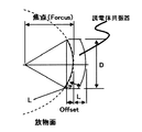
- the limiting surface (the place where this change occurs due to electromagnetic wave behavior) is called the “radiation fire surface”.
- the distance between the objects to be joined must be such that one is within the other radiant surface.
- the distance between the “near field” and the “radiant fire surface” is not clear, but power transmission in the region before becoming “radiative” according to the “coupled mode theory” in paragraph [0009] It is related to.
- the present invention has been made in view of the above circumstances, and a power transmission apparatus and method capable of transmitting power with high transmission efficiency over a wide range from a near field to a far field with a simple configuration, and It is an object of the present invention to provide a resonance device used therefor.
- a power transmission device that wirelessly transmits power from a first resonance device to a second resonance device,
- the first resonance device excites the first waveguide, the first dielectric resonator arranged coaxially with the first waveguide, and the first dielectric resonator.
- a first excitation structure for The first waveguide has one end as an open end and the other end as a short-circuit end,
- the first dielectric resonator has two first end faces located on opposite sides, and is insulated from the first waveguide in the vicinity of the open end of the first waveguide.
- a thickness that is disposed in the first waveguide and is a distance between the two first end faces is constant regardless of a radial position of the first dielectric resonator;
- the second resonance device excites the second waveguide, a second dielectric resonator arranged coaxially with the second waveguide, and the second dielectric resonator.
- a second excitation structure for The second waveguide has one end as an open end and the other end as a short-circuit end,
- the second dielectric resonator has two second end faces located on opposite sides, and is insulated from the second waveguide in the vicinity of the open end of the second waveguide.
- the second dielectric resonator is disposed in the second waveguide, and a thickness that is a distance between the two second end faces is constant regardless of a radial position of the second dielectric resonator;
- the first resonance device and the second resonance device are arranged such that an open end of the first waveguide and an open end of the second waveguide face each other, and
- the two first end faces or the two second end faces are substantially in a waveguide direction of the first waveguide or a waveguide direction of the second waveguide.
- the planes are mutually orthogonal planes parallel to each other.
- the two first end faces or the two second end faces are located farther from the second dielectric resonator or the first dielectric resonator at the center than at the outer periphery.
- at least one of the two first end faces or at least one of the two second end faces is at least at an outer peripheral portion, with the first waveguide or the second waveguide. It consists of at least a part of a conical surface, a pyramid surface, a spherical surface, a paraboloid or an ellipsoid having a coaxial symmetry axis.
- the shape of the first dielectric resonator or the second dielectric resonator is a polygonal column, a polygonal cylinder, or a cylinder having both end surfaces of the first end surface or the second end surface. Or it is a cylinder.
- a cross-sectional shape of the first waveguide or the second waveguide is a polygonal cylinder or a cylinder.
- the first waveguide or the second waveguide has a tapered shape in which a cross-sectional area gradually decreases from the open end to the short-circuit end.
- the first excitation structure or the second excitation structure is configured such that the first waveguide is short-circuited at the first waveguide or at the short-circuited end of the second waveguide.
- a conductor is disposed insulated from the wave tube or the second waveguide, and includes a conductor extending in the waveguide direction inside the first waveguide or inside the second waveguide. .
- the object as described above is achieved.
- the first resonance device and the second resonance device are arranged so that an open end of the first waveguide and an open end of the second waveguide face each other, and the first A power transmission method characterized by inputting power to the excitation structure and outputting power from the second excitation structure; Is provided.
- the object as described above is achieved.
- a resonant device used to configure the power transmission device or to implement the power transmission method described above A waveguide, a dielectric resonator disposed coaxially with the waveguide, and an excitation structure for exciting the dielectric resonator;
- the waveguide has an open end at one end and a short-circuited end at the other end,
- the dielectric resonator has two end faces located opposite to each other, and is disposed in the waveguide so as to be insulated from the waveguide in the vicinity of the open end of the waveguide, The thickness, which is the distance between the two end faces, is constant regardless of the radial position of the dielectric resonator,
- a power transmission device capable of transmitting power with high transmission efficiency over a wide range from a near field to a far field with a simple configuration.
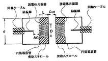
- Embodiment 1 of a power transmission device by the present invention. It is a figure which shows the relationship between the transmission distance in Embodiment 1, and transmission efficiency. It is a figure which shows the relationship between the transmission distance in Embodiment 1, and the frequency where transmission efficiency becomes the maximum. It is a figure which shows the relationship between an excitation line gap and transmission efficiency when the excitation line gap in Embodiment 1 is changed. It is a figure which shows the relationship between the length of an excitation line and transmission efficiency when the transmission distance in Embodiment 1 is 7.5 mm. It is a figure which shows S parameter when the transmission distance in Embodiment 1 is 7.5 mm.
- FIG. 10 is a diagram showing a relationship between transmission distance and transmission efficiency when the axial direction position of the dielectric resonator with respect to the cylindrical waveguide is set from the same plane to the inside or outside of the cylindrical waveguide in the TM02 ⁇ mode in the third embodiment.
- FIG. 10 is a diagram showing the relationship between transmission distance and transmission efficiency when the axial position of the dielectric resonator with respect to the cylindrical waveguide is set from the same plane to the inside or outside of the cylindrical waveguide for the TM03 ⁇ mode in the third embodiment. .
- FIG. 10 is a diagram showing S parameters when the waveguide distance in the fourth embodiment is between 10 mm and 50 mm.
- FIG. 9 is a schematic perspective view showing Embodiment 5 of the power transmission device according to the present invention and showing a dielectric resonator having a regular pentagonal prism shape. It is typical see-through
- FIG. 10 is a schematic perspective view showing an excitation structure in an eighth embodiment.
- FIG. 20 is a diagram illustrating a relationship between transmission distance and transmission efficiency in the eighth embodiment. It is a figure which shows the S parameter in Embodiment 8. It is a figure which shows the result of the electromagnetic field analysis by the electromagnetic field simulation in Embodiment 8. It is a typical see-through
- Embodiment 1A It is a typical see-through
- Embodiment 1A It is explanatory drawing of the effect
- a coil or an antenna is used as a resonator.
- a parallel plate type dielectric resonator having a highest Q value or a similar dielectric resonator is used in the microwave.
- An electric power transmission apparatus that further increases the transmission distance.
- a dielectric resonator similar to a parallel plate dielectric resonator is not a parallel plate shape, but a shape in which the thickness, which is the distance between two end faces, is constant regardless of the radial position of the dielectric resonator.
- the dielectric resonator of FIG. the parallel plate type dielectric resonator will be mainly described. However, the same applies to a dielectric resonator similar to the parallel plate type dielectric resonator.
- each parallel plate type dielectric resonator the parallel end face is provided in order to realize the required electromagnetic shielding. Of these, only the surface facing the parallel end surface of the other parallel plate type dielectric resonator is opened, and the other surface is covered with a waveguide.
- a resonator having a high Q value since a resonator having a high Q value is provided, even if the coupling coefficient K is small, K ⁇ Q (or KQ), which is an index of transmission efficiency, can be kept large, and high transmission efficiency can be achieved. Can keep. Furthermore, according to the present invention, since the parallel plate type dielectric resonator has various resonance modes, the facing area can be made larger than that of the coil or the antenna, and the coupling coefficient K can be increased. KQ can be further increased. Thus, according to the present invention, a power transmission device is provided in which transmission efficiency does not decrease even when the transmission distance is further increased.
- the Q value of the resonance system is large by adopting a structure that radiates electromagnetic waves in one direction, even if the coupling coefficient K is extremely small, the radiation is radiated from one dielectric resonator.
- a power transmission device that can efficiently receive electromagnetic waves at the other dielectric resonator, and can therefore transmit power to a far field with high transmission efficiency.
- a transmission apparatus can be provided at low cost with a small number of parts.
- the two first end faces or the two second end faces are located farther from the outer periphery than the second dielectric resonator or the first dielectric resonator.
- At least one of the one end faces or at least one of the two second end faces at least at the outer periphery, a conical surface having a symmetry axis coaxial with the first waveguide or the second waveguide, a pyramid surface, a spherical surface,
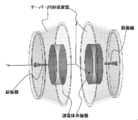
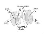
- FIG. 1 is a schematic cross-sectional view showing the first embodiment.
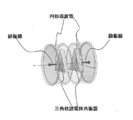
- the power transmission device of the present embodiment wirelessly transmits power from the first resonance device (arranged on the left side in FIG. 1) to the second resonance device (arranged on the right side in FIG. 1). It is a power transmission device.
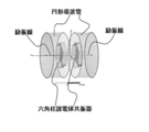
- the first resonance device includes a first waveguide (a cylindrical waveguide having a cylindrical cross section (also referred to as “circular waveguide”) located on the left side in FIG. 1), and a first dielectric resonator ( 1 includes a cylindrical dielectric resonator located on the left side and a first excitation structure for exciting the first dielectric resonator (in FIG. 1, the central conductor of the coaxial cable located on the left side). Excitation line).
- the first waveguide, the first dielectric resonator, and the first excitation structure are arranged coaxially.
- coaxial refers to a state in which they are arranged “so that they share a shaft”.
- the first waveguide has one end (right end in FIG.
- the first dielectric resonator has two first parallel end faces parallel to each other and located on opposite sides (both end faces located on the left side and the right side in FIG. 1), and the first parallel end faces are the first parallel end faces. Insulated from the first waveguide in the vicinity of the open end of the first waveguide so as to be substantially orthogonal to the waveguide direction (left-right direction in FIG. 1) of the waveguide (FIG. 1). 1 is arranged in the first waveguide (with a cylindrical foam polystyrene located on the left side).
- the second resonance device has a structure equivalent to that of the first resonance device as described above, but is arranged in the opposite direction to the first resonance device. That is, the second resonance device includes a second waveguide (cylindrical waveguide having a cylindrical cross section located on the right side in FIG. 1) and a second dielectric resonator (a cylinder located on the right side in FIG. 1). And a second excitation structure for exciting the second dielectric resonator (excitation line composed of the central conductor of the coaxial cable located on the right side in FIG. 1). .
- the second waveguide, the second dielectric resonator, and the second excitation structure are arranged coaxially. One end (left end in FIG.
- the second dielectric resonator has two second parallel end faces (both end faces located on the left and right sides in FIG. 1) that are parallel to each other and opposite to each other, and the first parallel end faces are the second parallel end faces. Insulated from the second waveguide in the vicinity of the open end of the second waveguide so as to be substantially orthogonal to the waveguide direction of the waveguide (left-right direction in FIG. 1) (FIG. 1). 1 is disposed in the second waveguide (with a cylindrical foam polystyrene located on the right).
- the first resonance device and the second resonance device are arranged coaxially so that the open end of the first waveguide and the open end of the second waveguide face each other.
- the electric power input to the second excitation structure is output from the second excitation structure.
- the resonance frequency is set near 2.45 GHz and the TM01 ⁇ mode is used.
- the resonator is a parallel plate type dielectric resonator, its thickness is equal to the axial dimension, ie, length L of the resonator.
- a coaxial cable with a center conductor that is, a center conductor having an excitation line length of about 30.6 mm) having a length of about 1/4 wavelength (about 30.6 mm at 2.45 GHz) is exposed to a cylindrical waveguide and a cylindrical shape.
- the transmission distance (M) is a distance between two resonance devices, and in particular, the first waveguide of the first resonance device or the second waveguide of the first dielectric resonator and the second resonance device. It is the minimum distance among the distances between the tube and the second dielectric resonator.
- the transmission distance (M) is typically the smaller one of the distance Cut between the two waveguides facing each other and the distance between the two dielectric resonators facing each other. In the present embodiment, typically, the distance Cut between two cylindrical waveguides facing each other is equal to the distance between two dielectric resonators facing each other.
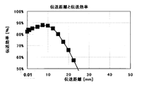
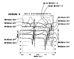
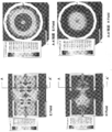
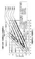
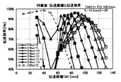
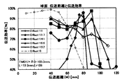
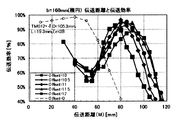
- Fig. 2 shows the transmission characteristics (relationship between transmission distance and transmission efficiency) measured as the transmission efficiency, which is the ratio of output power to input power.
- the transmission efficiency reaches a maximum of about 88% near a transmission distance of 7.5 mm, and the transmission efficiency becomes small whether the distance is closer or further away.
- the transmission distance at which the transmission efficiency is 50% is about 25 mm.
- This transmission distance is 0.20 times the wavelength ⁇ (in Table 1, the number of times this wavelength ⁇ is indicated in the column “Wavelength ( ⁇ )”), and the wavelength ⁇ which is the limit of the near field It is larger than 0.16 times and reaches the far field.
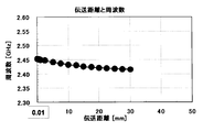
- FIG. 3 shows the relationship between the transmission distance and the frequency that maximizes the transmission efficiency. It can be seen that the change in resonance frequency is as small as 40 MHz.
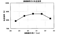
- FIG. 4 shows transmission characteristics (relationship between excitation line gap and transmission efficiency) when the gap (axial distance: excitation line gap) between the excitation line and the dielectric resonator is changed.
- the transmission efficiency reaches almost the maximum in the vicinity of the gap of 23 mm.
- Fig. 5 shows the relationship between the length of the excitation line and the transmission efficiency when the transmission distance is 7.5 mm. Since the actual frequency is lower than 2.45 GHz, the transmission efficiency reaches almost the maximum in the vicinity of the excitation line length of 30.6 mm.
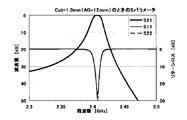
- FIG. 6 shows S parameters when the transmission distance is 7.5 mm.
- the first peak has a frequency of 2.437 GHz, the attenuation of S21 is 0.56 dB, and the return loss of S11 is 24 dB.
- the second peak has a frequency of 2.364 GHz, S21 is 16 dB, and S11 is 1.5 dB.
- the two opposing dielectric resonators are electric field coupled, and the coupling coefficient K is 0.030.
- FIG. 7 shows the relationship between the transmission distance and the transmission efficiency when the two units are changed from coaxial to the inter-axis distances of 5 mm, 10 mm, and 15 mm (that is, the axes are shifted).
- the transmission efficiency drops sharply when the axis is shifted by 5 mm, and falls below 50%.
- FIG. 8 shows the relationship between the transmission distance and the transmission efficiency when it is set to be one (same position), but set to the inside or outside of the cylindrical waveguide from the same plane. If the dielectric resonator is placed 5 mm outside the circular waveguide, the transmission efficiency decreases, and decreases rapidly with the transmission distance. If the dielectric resonator is placed about 5 to 10 mm from the inside of the circular waveguide, the transmission efficiency increases and the transmission distance also increases. However, the dielectric resonator is flush with the inside of the circular waveguide. 15 mm, the transmission efficiency increases up to a transmission distance of about 7.5 mm, but after that, the transmission efficiency is almost the same as in the case of the same level.
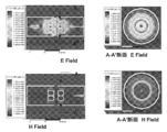
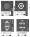
- Fig. 9 shows the result of electromagnetic field analysis performed in electromagnetic field simulation. Since there is no circumferential electromagnetic field change, one radial electromagnetic field change and one axial electromagnetic field change, it can be confirmed that the mode of the dielectric resonator is the TE01 ⁇ mode. Further, since the electric field between the waveguides is strong, it can be confirmed that the dielectric resonators are mainly coupled by the electric field.
- Patent Document 2 it is assumed that a dielectric resonator is inserted into the cutoff waveguide, but in Embodiment 1 of the present invention, the diameter of the cylindrical waveguide is 50.6 mm, and the cutoff frequency of the TM01 mode of the cylindrical waveguide is Is 4.54 GHz, TM11 mode cutoff frequency is 7.23 GHz, TM02 mode cutoff frequency is 10.40 GHz, TE11 mode cutoff frequency is 3.47 GHz, TE21 mode cutoff frequency is 5.77 GHz, TE01 mode cutoff frequency Since it is 7.23 GHz, it is a condition below the cut-off frequency.
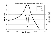
- FIG. 10A shows the S parameter when the interval (Cut) between the waveguides is 0.5 mm.
- FIG. 10b shows the S parameter when the gap (AG) between the end of the coaxial cable (ie, the end of the excitation line) and the dielectric resonator is changed from 23 mm to 12 mm.
- This characteristic is a two-stage bandpass filter having a center frequency of 2.407 GHz, a bandwidth of about 6 MHz, and an insertion loss of about 0.2 dB (transmission efficiency of about 95%).
- FIG. 10C shows the S parameter when the interval between the cylindrical waveguides is 1.0 mm.
- This characteristic is a two-stage bandpass filter having a center frequency of 2.4075 GHz, a bandwidth of about 5 MHz, and an insertion loss of about 0.2 dB (transmission efficiency of about 95%).
- a power transmission device having a waveguide distance of 0.5 mm or 1.0 mm can be applied to applications that require low loss and noise reduction, such as non-contact connectors and waveguide rotary joints.
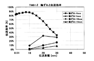
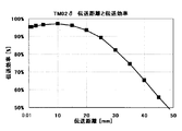
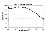
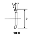
- a cylindrical dielectric resonator using a dielectric ceramic material having a relative dielectric constant of 38 is used, and a TM02 ⁇ mode and a TM03 ⁇ mode designed in the vicinity of 2.45 GHz are used.
- the TM02 ⁇ mode dielectric resonator has a diameter D of 55.6 mm, a length L of 16.0 mm, and a cylindrical waveguide has a diameter d of 100.1 mm.
- the TM03 ⁇ mode dielectric resonator has a diameter D of 80.4 mm, the length L is 16.3 mm, and the diameter d of the cylindrical waveguide is 144.8 mm.
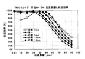
- the transmission distance at which the transmission efficiency of the TM02 ⁇ mode is 50% is around 48 mm. This transmission distance is 0.40 times the wavelength ⁇ , which is larger than 0.16 times the wavelength ⁇ , which is the limit of the near field, and is far field.
- the transmission distance at which the transmission efficiency of the TM03 ⁇ mode is 50% is around 66 mm, and this transmission distance is 0.54 times the wavelength ⁇ and is larger than 0.16 times the wavelength ⁇ , which is the limit of the near field. You can see that the far field has been reached.
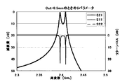
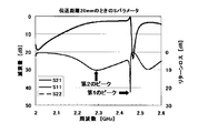
- S-parameters of the TM02 ⁇ mode and the TM03 ⁇ mode when the waveguide distance, that is, the transmission distance is 20 mm are shown in FIGS. 13 and 14, respectively.
- the first peak has a frequency of 2.450 GHz, the attenuation of S21 is 0.53 dB, and the litter loss of S11 is 50 dB.
- the second peak has a frequency of 2.371 GHz, S21 is 5 dB, and S11 is 6.5 dB.
- the first peak has a frequency of 2.486 GHz, the attenuation of S21 is 0.35 dB, and the litter loss of S11 is 37 dB.
- the second peak has a frequency of 2.441 GHz, S21 is 9 dB, and S11 is 3 dB.
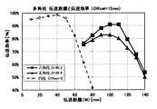
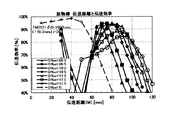
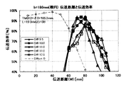
- FIG. 15 shows the relationship between the transmission distance and the transmission efficiency when the two units are changed from coaxial to 5 mm, 10 mm, 15 mm, 20 mm, 25 mm, and 30 mm (ie, the axes are shifted) for the TM02 ⁇ mode.
- the TM03 ⁇ mode is shown in FIG. In the TM02 ⁇ mode, when the transmission distance is 30 mm, the transmission efficiency is reduced by several percent compared to when the axis is displaced by 5 mm, and the transmission efficiency is maintained at 50% or more even when the axis is displaced by 15 mm.
- the transmission efficiency is reduced by several percent compared to when the axis is displaced by 5 mm, and even if the axis is displaced by 20 mm, the transmission efficiency is maintained at 50% or more. Yes.
- the end face of the dielectric resonator on the side facing the other unit is not flush with the open end of the cylindrical waveguide.
- the relationship between the transmission distance and the transmission efficiency when set inside or outside the cylindrical waveguide is shown in FIG. 17 for the TM02 ⁇ mode and in FIG. 18 for the TM03 ⁇ mode.
- the transmission efficiency is reduced by 10%, and the transmission efficiency is further reduced as the transmission distance is increased.
- the transmission efficiency decreases by several percent every time about 5 mm from the surface.
- the transmission efficiency is reduced by several percent in the range from 5 mm to 5 mm inside the dielectric resonator on the outer side of the cylindrical waveguide. .
- the results of the electromagnetic field analysis performed in the electromagnetic field simulation are shown in FIG. 19 for the TM02 ⁇ mode and in FIG. 20 for the TM03 ⁇ mode.
- the TM02 ⁇ mode there is no change in the magnetic field in the circumferential direction, two changes in the magnetic field in the radial direction, and one change in the electromagnetic field in the axial direction, so it can be confirmed that the mode of the dielectric resonator is the TE02 ⁇ mode. Further, since the electric field between the waveguides is strong, it can be confirmed that the dielectric resonators are mainly coupled by the electric field.
- the mode of the dielectric resonator is the TE03 ⁇ mode. Further, since the electric field between the waveguides is strong, it can be confirmed that the dielectric resonators are mainly coupled by the electric field.
- the cutoff frequency is Is also a high frequency condition. Since a TE03 ⁇ mode circular waveguide having a diameter of 144.8 mm is used, the TM01 of the cylindrical waveguide mode, which is the same mode as the dielectric resonator, and the TE11 mode / TE21 mode are higher than the cutoff frequency. This is a frequency condition.
- the dielectric resonator having a diameter D of 60.6 mm, a length L of 14.0 mm, and a cylindrical waveguide having a diameter d of 109.1 mm was also implemented (Table 1). reference).
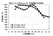
- Embodiment 4 a cylindrical dielectric resonator using a dielectric ceramic material having a relative dielectric constant of 38 is used, and a TM012 + ⁇ mode designed in the vicinity of 2.45 GHz is used.
- the dielectric resonator has a diameter D of 100.0 mm, a length L of 26.51 mm, and a cylindrical waveguide having a diameter d of 180 mm.
- FIG. 21 shows the relationship between the transmission distance and the transmission efficiency when the unit is changed from the coaxial shape (that is, the axis is shifted).
- the transmission distance at which the transmission efficiency is 50% when there is no axis deviation is 72.5 mm.
- This transmission distance is 0.59 times the wavelength ⁇ , and is larger than 0.16 times the wavelength ⁇ , which is the limit of the near field, and reaches the far field.
- the maximum transmission efficiency is shown near a transmission distance of 50 mm. The greater the shaft misalignment, the lower the transmission efficiency. Over 70 mm.
- the S parameter when the waveguide distance is between 10 mm and 50 mm is shown in FIG.
- the frequency of the first peak of S11 decreases as the waveguide distance increases.
- the second peak becomes slightly higher as the waveguide distance increases, and is not visible when the waveguide distance is 20 mm to 30 mm, and is not observed at all at 40 mm or 50 mm. That is, the coupling coefficient is not observed from near 19 mm which is 0.16 times the wavelength ⁇ , which is the limit of the near field, and power is transmitted even if there is no coupling coefficient.
- FIG. 23 shows the relationship between the transmission distance and the transmission efficiency when set inside or outside the cylindrical waveguide. Up to a transmission distance of 30 mm, the transmission efficiency is maintained at 90% or more except when the dielectric resonator is set to 5 mm outside the cylindrical waveguide, and after the transmission distance of 40 mm, the resonator moves inward from the open end of the waveguide. Transmission efficiency decreases rapidly in order from one.
- the dielectric resonator when the transmission distance (distance between the waveguides) is 60 mm, the dielectric resonator is placed 0 mm, 5 mm, 10 mm, and 15 mm inside (the distance between the dielectric resonators is 60 mm, 65 mm, 70 mm, and 75 mm). And the coupling between the dielectric resonators is reduced, and the transmission efficiency is drastically reduced. However, even if the resonator is 15 mm inside from the open end of the waveguide, the transmission efficiency is 50% or more up to a transmission distance of 60 mm.
- FIG. 24 shows the result of the electromagnetic field analysis performed in the electromagnetic field simulation.
- the TM01 mode, the TM11 mode, the TE11 mode, the TE21 mode, and the TE01 mode which are the same cylindrical waveguide modes as the dielectric resonator.
- a cutoff waveguide a filter is configured with a frequency equal to or lower than the cutoff frequency
- the cutoff frequency is used in any mode.
- a TM012 + ⁇ mode designed in the vicinity of 2.45 GHz is used by using a polygonal columnar dielectric resonator using a dielectric ceramic material having a relative dielectric constant of 38.
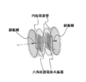
- FIG. 25 shows a schematic perspective view when the dielectric resonator has a regular triangular prism shape
- FIG. 26 shows a schematic perspective view when the dielectric resonator has a regular square prism shape
- FIG. 27 shows a schematic perspective view in the case where is a regular pentagonal prism shape
- FIG. 28 shows a schematic perspective view in the case where the dielectric resonator is a regular hexagonal prism shape.
- Table 1 The dimensions of the dielectric resonator of each shape are shown in Table 1 described later.
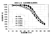
- FIG. 29 shows the relationship between the transmission distance and the transmission efficiency depending on the shape of the dielectric resonator in the present embodiment.
- the diameter D of the resonator shown in the fourth embodiment is about 100 mm
- the length L of the resonator is about 19 mm
- the cylindrical waveguide has a cylindrical shape.
- the diameter d is 180 mm.
- the transmission distance at which the transmission efficiency is 50% is 68 mm when the dielectric resonator shape is a quadrangular prism and a pentagonal prism, and this transmission distance is 0.56 times the wavelength ⁇ , which is the limit of the near field. It can be seen that it is larger than 0.16 times the wavelength ⁇ and reaches the far field.
- the transmission distance at which the transmission efficiency is 50% is 72 mm when the dielectric resonator shape is a triangular prism and a hexagonal prism, and this transmission distance is 0.59 times the wavelength ⁇ , which is the limit of the near field. It can be seen that it is larger than 0.16 times ⁇ and reaches the far field.
- the resonance mode can be changed to the TM012 + ⁇ mode by designing the diameter of the inscribed circle to be about 100 mm.
- the loss can be maintained at 90% or more up to a transmission distance of 50 mm.
- the triangular prism and the quadrangular prism many modes are generated, and there are many regions that do not directly contribute to resonance, and this region is close to the inner cylinder of the cylindrical waveguide, so that the Q value is deteriorated. Due to these factors, the transmission loss is gradually reduced.
- FIG. 30 shows the result of electromagnetic field analysis performed in electromagnetic field simulation to confirm that the hexagonal column-shaped dielectric resonator is resonating with TM012 + ⁇ as in the fourth embodiment. Since there is no circumferential magnetic field change, one radial magnetic field change and two axial electromagnetic field changes, it can be confirmed that the mode of the dielectric resonator is the TE012 + ⁇ mode. Further, since the electric field between the waveguides is strong, it can be confirmed that the dielectric resonators are mainly coupled by the electric field.
- the coupling between the resonators is not observed when the transmission distance is around 20 to 30 mm.
- the waveguide having an outer diameter of 187 to 216 mm since the waveguide having an outer diameter of 187 to 216 mm is used, the TM01 mode, the TM11 mode, the TE11 mode, the TE21 mode, and the TE01, which are the same cylindrical waveguide modes as the dielectric resonator.
- the condition is equal to or higher than the cut-off frequency
- Patent Document 2 it is assumed that a cut-off waveguide (a filter is configured with a frequency lower than the cut-off frequency) is used.
- a power transmission device that maintains high transmission efficiency at a frequency higher than the frequency has been realized.
- Embodiment 6 a cylindrical dielectric resonator using a dielectric ceramic material having a relative dielectric constant of 20 is used, and a TM012 + ⁇ mode designed in the vicinity of 2.45 GHz is used.
- Dielectric resonator diameter D is 100 mm and length L is 26.51 mm
- cylindrical waveguide diameter d is 180 mm
- dielectric resonator diameter D is 140 mm and length L is 29.5 mm
- cylinder A waveguide having a diameter d of 216 mm was used.
- FIG. 31 shows the relationship between the transmission distance and the transmission efficiency in this embodiment.
- the transmission distance when the transmission efficiency is 50% is 103 mm.
- This transmission distance is 0.84 times the wavelength ⁇ , and the wavelength ⁇ is the limit of the near field. It is larger than 0.16 times and reaches the far field.
- the diameter of the dielectric resonator is 140 mm, the transmission distance when the transmission efficiency is 50% is 120 mm.
- This transmission distance is 0.98 times the wavelength ⁇ , and the wavelength ⁇ is the limit of the near field. It is larger than 0.16 times and reaches the far field.
- Example 6 since a circular waveguide having a diameter of 216 mm is used, the TM01 mode, the TM11 mode, the TE11 mode, the TE21 mode, and the TE01 mode, which are the same cylindrical waveguide modes as the dielectric resonator, are used.
- a cutoff waveguide (a filter is configured with a frequency equal to or lower than the cutoff frequency) is used in Patent Document 2, but in the present embodiment, the cutoff frequency is used in any mode.
- the cutoff frequency is used in any mode.
- FIG. 32 shows a resonance mode when the transmission distance is 50 mm in a dielectric resonator having a diameter D of 100 mm
- FIG. 33 shows a resonance mode when the transmission distance is 20 mm in a dielectric resonator having a diameter D of 140 mm
- FIG. 34 shows a resonance mode when the transmission distance is 70 mm in a dielectric resonator having a diameter D of 140 mm.
- the mode of the dielectric resonator is TE012 + ⁇ .
- the mode can be confirmed.
- a dielectric resonator having a diameter D of 140 mm and a transmission distance of 20 mm there is no circumferential magnetic field change, one radial magnetic field change and two axial electromagnetic field changes.
- This mode can be confirmed to be the TE012 + ⁇ mode.
- a dielectric resonator having a diameter D of 140 mm and a transmission distance of 70 mm when the phase is 0 degree, there is no circumferential magnetic field change, one radial magnetic field change, and an axial electromagnetic field change.
- the mode of the dielectric resonator is the TE012 + ⁇ mode, but when the phase is around 90 degrees, there is no circumferential magnetic field change, four radial magnetic field changes, and an axial electromagnetic field. Since the change is one, the resonance mode of the TE04 ⁇ mode is also generated, and it can be seen that the mode of the dielectric resonator is a hybrid mode of the TE012 + ⁇ mode and the TE04 ⁇ mode.
- FIG. 35 shows a schematic perspective view of the apparatus of this embodiment.
- FIG. 36 shows the relationship between the transmission distance and the transmission efficiency in this embodiment.
- the transmission efficiency is 50%
- the transmission distance is 27 mm.
- This transmission distance is 1.08 times the wavelength ⁇ and is larger than 0.16 times the wavelength ⁇ , which is the limit of the near field, and reaches a sufficiently far field.
- the transmission efficiency is 80%
- the transmission distance is 21 mm.
- This transmission distance is 0.84 times the wavelength ⁇ , which is larger than 0.16 times the wavelength ⁇ , which is the limit of the near field, and reaches the far field. I understand that.
- FIG. 37 shows the S parameter when the transmission distance is 21 mm.
- the first peak has a frequency of 11.256 GHz, the value of S11 is 20 dB, and the value of S21 is 1.09 dB. 1.09 dB is 77.7% in transmission efficiency.
- the second peak is not observed. This is probably because the transmission distance far exceeds 4 mm, which is 0.16 times the wavelength ⁇ , which is the limit of the near field.
- the condition is equal to or higher than the cut-off frequency.
- a cut-off waveguide a filter is configured with a frequency equal to or lower than the cut-off frequency
- FIG. 38 shows the result of electromagnetic field analysis performed by electromagnetic field simulation.
- FIG. 38 shows the electromagnetic field distribution when the transmission distance is 21 mm. Since there is no circumferential magnetic field change, two radial magnetic field changes and one axial electromagnetic field change, it can be confirmed that the mode of the dielectric resonator is the TM02 ⁇ mode.
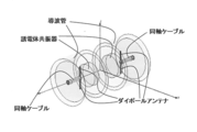
- a TE012 + ⁇ mode designed in the vicinity of 12 GHz is used using a cylindrical dielectric resonator using a dielectric ceramic material having a relative dielectric constant of 24.
- a cylindrical dielectric resonator having a diameter D of 14 mm and a length L of 3.75 mm was used.
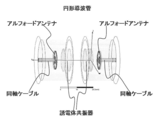
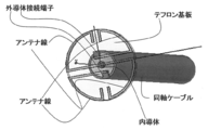
- a schematic perspective view of the apparatus of the present embodiment is shown in FIG.
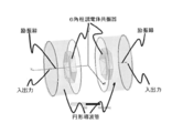
- FIG. 40 shows a schematic perspective view of the excitation structure in the present embodiment.
- This excitation structure is for exciting a cylindrical dielectric resonator in the TE mode, and is called an Alford antenna.
- An Alford antenna was attached to the tip of the cable, and the distance (gap) between the Alford antenna and the dielectric resonator was fixed at 3.0 mm.
- This is a unit (resonance device). Two of these are manufactured, the open ends of the cylindrical waveguides are made to face each other so as to be coaxial, and an arbitrary distance is maintained, and the coaxial cable of one unit (first resonance device) is placed near 12 GHz. The power is turned on, and the power is taken out from the coaxial cable of the other unit (second resonance device).
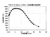
- FIG. 41 shows the relationship between the transmission distance and the transmission efficiency in this embodiment.
- the transmission efficiency is a maximum of about 90% within the transmission distance range of 3 mm to 9 mm, and the transmission efficiency is small regardless of whether the transmission distance is shorter or larger.
- the transmission distance at which the transmission efficiency is 50% is about 15.5 mm. This transmission distance is 0.62 times the wavelength ⁇ , and is larger than 0.16 times the wavelength ⁇ , which is the limit of the near field, and reaches the far field.
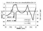
- the S parameter when the transmission distance is 105 mm is shown in FIG.
- the first peak has a frequency of 11.045 GHz, the attenuation of S21 is 0.86 dB, and the retard loss of S11 is 29 dB.
- the second peak has a frequency of 10.845 GHz, S21 is 2 dB, and S11 is 13 dB.
- the opposing dielectric resonators are magnetically coupled. If the first peak and the second peak indicate coupling, the coupling coefficient K is 0.0183.
- FIG. 43 shows the result of the electromagnetic field analysis performed in the electromagnetic field simulation. Since there is no circumferential electromagnetic field change, one radial electromagnetic field change and one axial electromagnetic field change, it can be confirmed that the mode of the dielectric resonator is the TE012 + ⁇ mode. Further, since the magnetic field between the waveguides is strong, it can be confirmed that the dielectric resonator is coupled mainly by the magnetic field.
- Patent Document 2 it is assumed that a dielectric resonator is inserted into the cutoff waveguide.
- the diameter of the cylindrical waveguide is 25.2 mm, and the cylinder is in the same mode as the dielectric resonator.
- the TE01 mode has a cutoff frequency of 14.52 GHz with a diameter of 25.2 mm
- the TE21 mode has a cutoff frequency of 11.58 GHz
- the TE11 mode has a cutoff frequency of 6.98 GHz
- the TM01 mode has a cutoff frequency of 9.11 GHz
- the filter is configured with a frequency equal to or lower than the cut-off frequency. Power transmission device is realized to maintain a high transmission efficiency by the number or frequency.
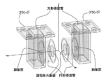
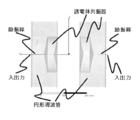
- a structure including a coaxial cable and a half-wavelength dipole antenna connected thereto may be used as the excitation structure of the dielectric resonator.
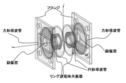
- the excitation structure of the dielectric resonator a structure that supplies power from a rectangular waveguide as shown in FIG. 45 may be used.
- the resonator can be excited in the TM mode.
- the excitation structure of the dielectric resonator a structure that supplies power from a rectangular waveguide as shown in FIG. 46 may be used. In this case, the resonator can be excited in the TE mode.
- an excitation line having a wavelength of about 1/4 is extended from the inner surface of the waveguide so as to be orthogonal to the radial direction as shown in FIG. 47, and power is supplied from a tap in the middle of the excitation line. It is also possible to use one that supplies. In this case, the resonator can be excited in the TE mode.
- the first or second waveguide may have a tapered shape in which the cross-sectional area gradually decreases from the open end to the short-circuit end.
- the relative dielectric constant of the dielectric resonator used in the resonator is larger.
- the diameter D of the dielectric resonator is 100 mm and the resonance mode is TE012 + ⁇ mode.
- the transmission distance at which the transmission efficiency is 50% is 72.5 mm in the fourth embodiment.
- the transmission distance is 103 mm when the relative dielectric constant is 20.
- the transmission distance is increased as the diameter D of the dielectric resonator is larger. be able to.
- FIG. 49 shows a graph in which the diameter D and the length L of the dielectric resonator can be calculated by setting the frequency and the resonance mode of the cylindrical dielectric resonator.
- the resonance mode By selecting the resonance mode, determining one point on the graph (straight line) corresponding to the selected mode, reading the numerical value on the vertical axis of this point, and determining the value of wavelength ⁇ and the value of relative dielectric constant Er, the diameter The value of D is obtained.
- the value of the length L is obtained by reading the numerical value on the horizontal axis at one point and using the obtained D value.
- the example shown in the embodiment is plotted.
- the electromagnetic field generated from a conductor or the like which is called a near field in the conventional technology, is in a state before the electromagnetic wave of the radio wave is still in an electromagnetic wave state.
- the coupling efficiency K and the transmission distance are related by the coupling coefficient K and the resonator Q, but according to the present invention, the coupling is achieved by using a parallel plate dielectric resonator in the resonance system.
- An apparatus is provided in which power is transmitted continuously even at distances greater than the minimum distance formed, i.e., from the near field to the far field.
- the use of a dielectric resonator makes it easy to face the surfaces of the dielectric resonator larger than the wavelength or the length of wavelength 1 ⁇ 2.
- a dielectric resonator having a diameter of about 122.5 mm can be placed in a cylindrical waveguide to obtain a transmission distance of more than half a wavelength.
- the present invention is an apparatus that can continuously transmit power from the near field to the far field regardless of whether the waveguide is in the cutoff region or not as shown in Patent Document 2.
- the present invention is a power transmission device that can handle large power because of its high transmission efficiency.
- the two first end faces or the two second end faces are parallel to each other substantially perpendicular to the waveguide direction of the first waveguide or the waveguide direction of the second waveguide. It consisted of a single flat surface. That is, in the above embodiment, the first end face is the first parallel end face, and the second end face is the second parallel end face.
- the two first end faces or the two second end faces are centered from the second dielectric resonator or the first dielectric resonator from the outer peripheral portion. Those located further away are shown below with individual example numbers.
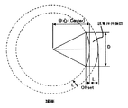
- Embodiment A1 Configuration diagrams of Embodiment A1 are shown in FIGS. 50a and 50b.
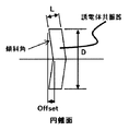
- each dielectric resonator the first dielectric resonator or the second dielectric resonator
- one of the two end surfaces is a concave conical surface, and the surface normal direction of the one end surface That is, the thickness L, which is the distance between the two end faces, is constant regardless of the radial position of the dielectric resonator.
- the dielectric resonator has a relative dielectric constant of 38, a diameter D of 105.3 mm, and a thickness L of 19.3 mm.
- the diameter of the short-circuited circular waveguide is 1.8 times the diameter D of the dielectric resonator, that is, 189.5 mm.
- the dielectric resonator is located at substantially the same axial position as the open side of the circular waveguide.
- a conductor having a length of about 1 ⁇ 4 wavelength (30.6 mm) is positioned as an excitation line in the axial direction of the dielectric resonator from the center of the waveguide short-circuit surface, and between the excitation line and the dielectric resonator.
- An interval of 23 mm is set, the respective centers are aligned with the central axis of the dielectric resonator, and the open sides of the two cylindrical waveguides are faced to keep an arbitrary distance.
- the excitation line is attached to substantially the center of the short-circuit surface of the circular waveguide, and the central conductor of the coaxial connector is connected to the excitation line.
- a microwave of about 2.45 GHz is supplied to the excitation line through one coaxial connector.
- Microwave power resonates one dielectric resonator from one excitation line, resonates the other dielectric resonator maintained at an arbitrary distance, and the power transmitted to the other excitation line is the other. It is taken out from the coaxial connector. In this way, microwave power is transmitted from the connector of one circular waveguide to the connector of the other circular waveguide.
- the transmission characteristics are shown in FIG.
- the dielectric resonators resonate in the TM mode with excitation lines, and the dielectric resonators are coupled by electric field coupling and operate like a two-stage filter.
- FIG. 52 describes the operation or function of this embodiment.
- 52A to 52C show a case where the distance between two dielectric resonators, that is, the transmission distance M is approximately half the diameter D of the dielectric resonator.
- 52 (a) and 52 (b) since the end face of the dielectric resonator is a flat surface, the electromagnetic field generated from the outer peripheral portion of one of the dielectric resonators, particularly the outer peripheral edge, spreads outward in the radial direction. Thus, an electromagnetic field portion that does not pass through the other dielectric resonator is generated.
- FIG. 52 shows the operation or function of this embodiment.
- 52 (c) since the end surfaces facing each other of the two dielectric resonators are conical surfaces, the electromagnetic field generated from the outer peripheral portion of one dielectric resonator, particularly the outer peripheral edge, is Compared with the cases of FIGS. 52A and 52B, many portions including the expanded portion D ′ pass through the other dielectric resonator without expanding outward in the radial direction.
- 52D and 52E show a case where the distance between two dielectric resonators, that is, the transmission distance M is substantially equal to the diameter D of the dielectric resonator. Similarly in this case, in FIG.
- the transmission distance with a transmission efficiency of 50% reaches 115 mm, which is 40 mm longer than when the end face is not inclined (transmission distance 75 mm).
- the end face of the dielectric resonator is formed of a conical surface over the entire radial region from the outer peripheral portion to the central portion, but as one modification, as shown in FIG. Only the outer peripheral area is composed of a conical surface and the central area is configured as a truncated cone surface (conical dish surface) composed of a plane orthogonal to the axial direction, and the opposite end surface is configured so that the thickness of the dielectric resonator is constant. May be. About the boundary position of an outer peripheral part area
- Embodiment A2 The block diagram of Embodiment A2 is shown in FIG. 53 and FIG.
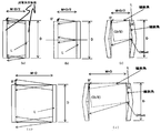
- the outer peripheral surface has a hexagonal prism shape, and one of the two end surfaces is a recessed hexagonal pyramidal surface.
- the thickness L which is the dimension in the surface normal direction of one end face, that is, the distance between the two end faces, is constant regardless of the radial position of the dielectric resonator.
- the dielectric resonator has a relative permittivity of 38, an outer peripheral hexagonal circumscribed circle diameter of 110 mm, an inscribed circle diameter of 99.4 mm, a thickness L of 19 mm, and six in relation to a plane perpendicular to the axial direction.
- the inclination angle of the pyramid surface is 12 °.
- the diameter of the circular waveguide is 209 mm.
- the outer peripheral surface has a pentagonal prism shape, and one of the two end surfaces is recessed.
- the thickness L which is a pentagonal pyramid surface and is the dimension in the surface normal direction of one end face, that is, the distance between the two end faces, is constant regardless of the radial position of the dielectric resonator.
- the dielectric resonator has a relative dielectric constant of 38, a pentagonal outer peripheral diameter of 110 mm, an inscribed circle diameter of 95.3 mm, a thickness L of 19 mm, and a pentagonal pyramid with respect to a plane orthogonal to the axial direction.
- the inclination angle of the surface is 12 °.
- the diameter of the circular waveguide is 187 mm.
- the relationship between transmission efficiency and transmission distance is shown in FIG. The transmission distance with a transmission efficiency of 50% is expanded by 65 mm from 75 mm to 140 mm of the cylindrical dielectric resonator.
- the end face of the dielectric resonator is formed of a pyramid surface (polygonal pyramid surface) over the entire radial region from the outer peripheral part to the center part, but the pyramid is not limited to a pentagonal pyramid or a hexagonal pyramid,
- the outer peripheral region may be formed of a pyramidal surface, and the central region may be configured of a plane orthogonal to the axial direction.
- region it can set suitably so that an effect
- Embodiment A3 Configuration diagrams of Embodiment A3 are shown in FIGS. 56a and 56b.
- the two end faces are both spherical surfaces, and the radius of curvature of one end face is more dielectric than the radius of curvature of the other end face. It is larger by the thickness L of the body resonator. That is, the thickness L, which is the distance between the two end faces, is constant regardless of the radial position of the dielectric resonator.
- the dielectric resonator has a relative dielectric constant of 38, a diameter D of 105.3 mm, and a thickness L of 19 mm.
- the diameter of the circular waveguide is 189.5 mm.
- the relationship between transmission efficiency and transmission distance is shown in FIG.
- the end face of the dielectric resonator is made of a spherical surface over the entire radial region from the outer peripheral portion to the central portion, but as one modified example, only the outer peripheral portion region is made of a spherical surface.
- Embodiment A4 Configuration diagrams of Embodiment A4 are shown in FIGS. 58a and 58b.
- each dielectric resonator the first dielectric resonator or the second dielectric resonator
- one of the two end faces is a concave paraboloid, and the dimension in the surface normal direction of the one end face That is, the thickness L, which is the distance between the two end faces, is constant regardless of the radial position of the dielectric resonator.
- the dielectric resonator has a relative dielectric constant of 38, a diameter D of 105.3 mm, and a thickness L of 19.3 mm.
- the diameter of the circular waveguide is 189.5 mm.
- the end face of the dielectric resonator is made of a paraboloid over the entire radial region from the outer peripheral portion to the central portion, but as one modification, only the outer peripheral region is made of a paraboloid.
- the central region may be configured from a plane orthogonal to the axial direction.
- or a function which were demonstrated in Embodiment A1 may be exhibited favorably.
- FIG. 5 A configuration diagram of the embodiment A5 is shown in FIG.
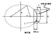
- each dielectric resonator (the first dielectric resonator or the second dielectric resonator)
- one of the two end faces is a concave ellipsoid, and the dimension of the one end face in the surface normal direction, that is, The thickness L, which is the distance between the two end faces, is constant regardless of the radial position of the dielectric resonator.
- the dielectric resonator has a relative dielectric constant of 38, a diameter D of 105.3 mm, and a thickness L of 19.3 mm.
- the diameter of the circular waveguide is 189.5 mm.
- the relationship between the transmission efficiency and the transmission distance is shown in FIG.
- FIG. 61 (ellipse minor axis length b fixed at 160 mm), FIG. 62 (elliptical minor axis length b fixed at 170 mm), and FIG. 63 (elliptical minor axis length).
- b is fixed to 180 mm).
- the end face of the dielectric resonator is made of an elliptical surface over the entire radial region from the outer peripheral part to the central part.
- the outer peripheral part region is made of an elliptical surface.
- You may comprise a partial area from the plane orthogonal to an axial direction.
- region it can set suitably so that an effect
- one of the first dielectric resonator and the second dielectric resonator has one of the end faces of the above embodiments A1 to A5, and the other is different from the above embodiments A1 to A5. It is good also as what has an end surface.
- one of the first dielectric resonator and the second dielectric resonator has one of the end faces of the first to eighth embodiments, and the other has the above-described embodiments A1 to A5. It is good also as having one of these end surfaces.
Abstract
Description
[2+K2×Q1×Q2-2×(1+K2×Q1×Q2)1/2]/[K2×Q1×Q2]
で表されるといわれている。
第1の共振装置から第2の共振装置へと無線で電力を伝送する電力伝送装置であって、
前記第1の共振装置は、第1の導波管と、該第1の導波管と同軸状に配置された第1の誘電体共振器と、該第1の誘電体共振器を励振するための第1の励振構造とを備えており、
前記第1の導波管は、一方端が開放端とされ且つ他方端が短絡端とされており、
前記第1の誘電体共振器は、互いに反対側に位置する2つの第1端面を有し、前記第1の導波管の開放端の近傍にて前記第1の導波管から絶縁されて前記第1の導波管内に配置されており、前記2つの第1端面間の距離である厚みが前記第1の誘電体共振器の径方向位置によらず一定であり、
前記第2の共振装置は、第2の導波管と、該第2の導波管と同軸状に配置された第2の誘電体共振器と、該第2の誘電体共振器を励振するための第2の励振構造とを備えており、
前記第2の導波管は、一方端が開放端とされ且つ他方端が短絡端とされており、
前記第2の誘電体共振器は、互いに反対側に位置する2つの第2端面を有し、前記第2の導波管の開放端の近傍にて前記第2の導波管から絶縁されて前記第2の導波管内に配置されており、前記2つの第2端面間の距離である厚みが前記第2の誘電体共振器の径方向位置によらず一定であり、
前記第1の共振装置と前記第2の共振装置とは、前記第1の導波管の開放端と前記第2の導波管の開放端とが互いに対向するように配置されており、前記第1の励振構造に入力された電力が前記第2の励振構造から出力されることを特徴とする電力伝送装置、
が提供される。
本発明の一態様においては、前記2つの第1端面または前記2つの第2端面は、外周部より中央部が前記第2の誘電体共振器または前記第1の誘電体共振器からより遠くに位置する。本発明の一態様においては、前記2つの第1端面の少なくとも一方または前記2つの第2端面の少なくとも一方は、少なくとも外周部において、前記第1の導波管または前記第2の導波管と同軸状の対称軸を持つ円錐面、角錐面、球面、放物面または楕円面の少なくとも一部からなる。
上記の電力伝送装置を用いて前記第1の共振装置から前記第2の共振装置へと無線で電力を伝送する電力伝送方法であって、
前記第1の共振装置と前記第2の共振装置とを前記第1の導波管の開放端と前記第2の導波管の開放端とが互いに対向するように配置し、前記第1の励振構造に電力を入力し、前記第2の励振構造から電力を出力することを特徴とする電力伝送方法、
が提供される。
また、本発明によれば、以上の如き目的を達成するものとして、
上記の電力伝送装置を構成するのに使用され或いは上記の電力伝送方法を実施するのに使用される共振装置であって、
導波管と、該導波管と同軸状に配置された誘電体共振器と、該誘電体共振器を励振するための励振構造とを備えており、
前記導波管は、一方端が開放端とされ且つ他方端が短絡端とされており、
前記誘電体共振器は、互いに反対側に位置する2つの端面を有し、前記導波管の開放端の近傍にて前記導波管から絶縁されて前記導波管内に配置されており、前記2つの端面間の距離である厚みが前記誘電体共振器の径方向位置によらず一定である、
ことを特徴とする共振装置、
が提供される。
図1は、実施形態1を示す模式的断面図である。本実施形態の電力電送装置は、第1の共振装置(図1では左側に配置されている)から第2の共振装置(図1では右側に配置されている)へと無線で電力を伝送する電力電送装置である。
実施形態1に於いて、円筒導波管に対する誘電体共振器の軸方向位置に関して、誘電体共振器を円筒導波管の内側に7.5mm挿入した2つのユニットを同軸状に配置し、円筒導波管同士の間隔(Cut)を0.5mmとしたときのSパラメータを図10aに示す。同軸ケーブルの先端(即ち励振線の先端)と誘電体共振器との間のギャップ(AG)を23mmから12mmに変更したときのSパラメータを図10bに示す。この特性は、中心周波数が2.407GHz、帯域幅が約6MHz、挿入損失が約0.2dB(伝送効率が約95%)である2段のバンドパスフィルタとなっている。また、円筒導波管同士の間隔を1.0mmとしたときのSパラメータを図10cに示す。この特性は、中心周波数が2.4075GHz、帯域幅が約5MHz、挿入損失が約0.2dB(伝送効率が約95%)である2段のバンドパスフィルタとなっている。導波管距離が0.5mmや1.0mmである電力伝送装置は非接触コネクタや導波管のロータリージョイントなどの、低損失でノイズの軽減が必要な用途に適用することができる。
実施形態3の装置の構造は、実施形態1のものと同等であり、図1に示されるものに該当する。
実施形態4の装置の構造は、実施形態1のものと同等であり、図1に示されるものに該当する。
実施形態5の装置の構造は、実施形態1のものと同等であり、図1に示されるものに該当する。
実施形態6の装置の構造は、実施形態1のものと同等であり、図1に示されるものに該当する。
実施形態7の装置の構造は、実施形態1のものと同等であり、図1に示されるものに該当する。
心導体の先端と誘電体共振器との間の距離(ギャップ)を4.5mmに保って固定した。本実施形態の装置の模式的透視斜視図を図35に示す。
実施形態8の装置の構造は、励振構造が後述のものであることを除いて、実施形態1のものと同等である。
図44に示すように、誘電体共振器の励振構造として、同軸ケーブル及びそれに接続された波長1/2のダイポールアンテナを含むものを用いても良い。

以上の実施形態では、2つの第1端面または2つの第2端面は、第1の導波管の導波方向または第2の導波管の導波方向に対して実質的に直交する互いに平行な単一の平面からなるものとした。即ち、以上の実施形態は、第1端面が第1平行端面であり、第2端面が第2平行端面である。
実施形態A1の構成図を、図50aおよび図50bに示す。ここでは、各誘電体共振器(第1の誘電体共振器または第2の誘電体共振器)において、2つの端面のうちの一方は凹んだ円錐面であり、一方の端面の面法線方向の寸法即ち2つの端面間の距離である厚みLは誘電体共振器の径方向位置によらず一定である。誘電体共振器は、比誘電率が38であり、直径Dが105.3mm、厚みLが19.3mmである。短絡円形導波管(短絡円筒導波管)の直径は誘電体共振器の直径Dの1.8倍すなわち189.5mmである。誘電体共振器は円形導波管の開放側とほぼ同じ軸方向位置に位置する。導波管短絡面の中心から誘電体共振器の軸方向に約1/4波長(30.6mm)の長さの導体を励振線として位置し、該励振線と誘電体共振器との間に23mmの間隔をとり、それぞれの中心を誘電体共振器の中心軸にあわせ、二つの円筒導波管の開放側同士を向き合わせ、任意の距離を保つ構成とする。励振線は円形導波管の短絡面のほぼ中心に取り付けられており、同軸コネクタの中心導体は励振線と接続されている。約2.45GHzのマイクロ波を、一方の同軸コネクタを経て励振線に供給する。マイクロ波電力は一方の励振線から一方の誘電体共振器を共振させ、さらに任意の距離を保ったもう一方の誘電体共振器を共振させ、もう一方の励振線に伝送された電力がもう一方の同軸コネクタより取り出される。このようにして、一方の円形導波管のコネクタから、もう一方の円形導波管のコネクタにマイクロ波電力が伝送される。伝送特性を図51に示す。誘電体共振器は励振線によりTMモードで共振し、誘電体共振器同士は電界結合により結合し2段のフィルタのように動作する。
実施形態A2の構成図を、図53および図54に示す。図53では、各誘電体共振器(第1の誘電体共振器または第2の誘電体共振器)において、外周面は六角柱形状であり、2つの端面のうちの一方は凹んだ六角錐面であり、一方の端面の面法線方向の寸法即ち2つの端面間の距離である厚みLは誘電体共振器の径方向位置によらず一定である。誘電体共振器は、比誘電率が38であり、外周面形状の六角形の外接円直径が110mm、内接円直径が99.4mm、厚みLが19mmで、軸方向に直交する平面に対する六角錐面の傾斜角が12°である。円形導波管の直径は209mmである。同様に、図54では、各誘電体共振器(第1の誘電体共振器または第2の誘電体共振器)において、外周面は五角柱形状であり、2つの端面のうちの一方は凹んだ五角錐面であり、一方の端面の面法線方向の寸法即ち2つの端面間の距離である厚みLは誘電体共振器の径方向位置によらず一定である。誘電体共振器は、比誘電率が38であり、外周面形状の五角形の外接円直径が110mm、内接円直径が95.3mm、厚みLが19mmで、軸方向に直交する平面に対する五角錐面の傾斜角が12°である。円形導波管の直径は187mmである。伝送効率と伝送距離との関係を図55に示す。伝送効率50%の伝送距離は円柱誘電体共振器の75mmから140mmヘと65mm拡大している。
実施形態A3の構成図を、図56aおよび図56bに示す。各誘電体共振器(第1の誘電体共振器または第2の誘電体共振器)において、2つの端面は、いずれも球面であり、一方の端面の曲率半径は他方の端面の曲率半径より誘電体共振器の厚みLだけ大きい。即ち、2つの端面間の距離である厚みLは誘電体共振器の径方向位置によらず一定である。誘電体共振器は、比誘電率が38であり、直径Dが105.3mm、厚みLが19mmである。円形導波管の直径は189.5mmである。伝送効率と伝送距離との関係を図57に示す。伝送効率50%の伝送距離は、Offset=14.1mmでは、Offset=0(凹みなしの円柱誘電体共振器)の75mmから95mmヘと20mm拡大している。
実施形態A4の構成図を、図58aおよび図58bに示す。各誘電体共振器(第1の誘電体共振器または第2の誘電体共振器)において、2つの端面のうちの一方は凹んだ放物面であり、一方の端面の面法線方向の寸法即ち2つの端面間の距離である厚みLは誘電体共振器の径方向位置によらず一定である。誘電体共振器は、比誘電率が38であり、直径Dが105.3mm、厚みLが19.3mmである。円形導波管の直径は189.5mmである。伝送効率と伝送距離との関係を図59に示す。伝送効率50%の伝送距離は、Offset=10.5mmでは、Offset=0(凹みなしの円柱誘電体共振器)の75mmから105mmヘと30mm拡大している。
実施形態A5の構成図を、図60に示す。各誘電体共振器(第1の誘電体共振器または第2の誘電体共振器)において、2つの端面のうちの一方は凹んだ楕円面であり、一方の端面の面法線方向の寸法即ち2つの端面間の距離である厚みLは誘電体共振器の径方向位置によらず一定である。誘電体共振器は、比誘電率が38であり、直径Dが105.3mm、厚みLが19.3mmである。円形導波管の直径は189.5mmである。伝送効率と伝送距離との関係を図61(楕円短軸の長さbを160mmに固定)、図62(楕円短軸の長さbを170mmに固定)及び図63(楕円短軸の長さbを180mmに固定)に示す。伝送効率50%の伝送距離は、楕円短軸の長さbのいずれに対しても、Offset=10~11mmにおいて、Offset=0(凹みなしの円柱誘電体共振器)の75mmから105mmヘと30mm拡大している。
本発明においては、第1の誘電体共振器及び第2の誘電体共振器を、一方が上記実施形態A1~A5のいずれかの端面を持つものとし、他方がそれと異なる上記実施形態A1~A5の端面を持つものとしてもよい。
Claims (10)
- 第1の共振装置から第2の共振装置へと無線で電力を伝送する電力伝送装置であって、
前記第1の共振装置は、第1の導波管と、該第1の導波管と同軸状に配置された第1の誘電体共振器と、該第1の誘電体共振器を励振するための第1の励振構造とを備えており、
前記第1の導波管は、一方端が開放端とされ且つ他方端が短絡端とされており、
前記第1の誘電体共振器は、互いに反対側に位置する2つの第1端面を有し、前記第1の導波管の開放端の近傍にて前記第1の導波管から絶縁されて前記第1の導波管内に配置されており、前記2つの第1端面間の距離である厚みが前記第1の誘電体共振器の径方向位置によらず一定であり、
前記第2の共振装置は、第2の導波管と、該第2の導波管と同軸状に配置された第2の誘電体共振器と、該第2の誘電体共振器を励振するための第2の励振構造とを備えており、
前記第2の導波管は、一方端が開放端とされ且つ他方端が短絡端とされており、
前記第2の誘電体共振器は、互いに反対側に位置する2つの第2端面を有し、前記第2の導波管の開放端の近傍にて前記第2の導波管から絶縁されて前記第2の導波管内に配置されており、前記2つの第2端面間の距離である厚みが前記第2の誘電体共振器の径方向位置によらず一定であり、
前記第1の共振装置と前記第2の共振装置とは、前記第1の導波管の開放端と前記第2の導波管の開放端とが互いに対向するように配置されており、前記第1の励振構造に入力された電力が前記第2の励振構造から出力されることを特徴とする電力伝送装置。 - 前記2つの第1端面または前記2つの第2端面は、前記第1の導波管の導波方向または前記第2の導波管の導波方向に対して実質的に直交する互いに平行な平面からなることを特徴とする、請求項1に記載の電力伝送装置。
- 前記2つの第1端面または前記2つの第2端面は、外周部より中央部が前記第2の誘電体共振器または前記第1の誘電体共振器からより遠くに位置することを特徴とする、請求項1に記載の電力伝送装置。
- 前記2つの第1端面の少なくとも一方または前記2つの第2端面の少なくとも一方は、少なくとも外周部において、前記第1の導波管または前記第2の導波管と同軸状の対称軸を持つ円錐面、角錐面、球面、放物面または楕円面の少なくとも一部からなることを特徴とする、請求項3に記載の電力伝送装置。
- 前記第1の誘電体共振器または前記第2の誘電体共振器の形状は、前記第1端面または前記第2端面を両端面とする多角柱、多角筒、円柱または円筒であることを特徴とする、請求項2に記載の電力伝送装置。
- 前記第1の導波管または前記第2の導波管の断面形状は、多角筒または円筒であることを特徴とする、請求項1乃至5のいずれか一項に記載の電力伝送装置。
- 前記第1の導波管または前記第2の導波管は、前記開放端から前記短絡端へと次第に断面積が小さくなるテーパー形状をなしていることを特徴とする、請求項1乃至5のいずれか一項に記載の電力伝送装置。
- 前記第1の励振構造または前記第2の励振構造は、前記第1の導波管の短絡端または前記第2の導波管の短絡端において前記第1の導波管または前記第2の導波管から絶縁されて配置され、前記第1の導波管の内部または前記第2の導波管の内部にて導波方向に延在する導体を含んでなることを特徴とする、請求項1乃至7のいずれか一項に記載の電力伝送装置。
- 請求項1乃至8のいずれか一項に記載の電力伝送装置を用いて前記第1の共振装置から前記第2の共振装置へと無線で電力を伝送する電力伝送方法であって、
前記第1の共振装置と前記第2の共振装置とを前記第1の導波管の開放端と前記第2の導波管の開放端とが互いに対向するように配置し、前記第1の励振構造に電力を入力し、前記第2の励振構造から電力を出力することを特徴とする電力伝送方法。 - 請求項1乃至8のいずれか一項に記載の電力伝送装置を構成するのに使用され或いは請求項9に記載の電力伝送方法を実施するのに使用される共振装置であって、
導波管と、該導波管と同軸状に配置された誘電体共振器と、該誘電体共振器を励振するための励振構造とを備えており、
前記導波管は、一方端が開放端とされ且つ他方端が短絡端とされており、
前記誘電体共振器は、互いに反対側に位置する2つの端面を有し、前記導波管の開放端の近傍にて前記導波管から絶縁されて前記導波管内に配置されており、前記2つの端面間の距離である厚みが前記誘電体共振器の径方向位置によらず一定である、
ことを特徴とする共振装置。
Priority Applications (3)
| Application Number | Priority Date | Filing Date | Title |
|---|---|---|---|
| JP2014507764A JP5850282B2 (ja) | 2012-03-30 | 2013-03-21 | 電力伝送の装置及び方法、並びにそれに用いる共振装置 |
| EP13769519.3A EP2833512B1 (en) | 2012-03-30 | 2013-03-21 | Method and device for power transmission and resonance device used in same |
| US14/389,748 US9577477B2 (en) | 2012-03-30 | 2013-03-21 | Power transmission apparatus and method, and resonance device used therein |
Applications Claiming Priority (4)
| Application Number | Priority Date | Filing Date | Title |
|---|---|---|---|
| JP2012-082365 | 2012-03-30 | ||
| JP2012082365 | 2012-03-30 | ||
| JP2012199469 | 2012-09-11 | ||
| JP2012-199469 | 2012-09-11 |
Publications (1)
| Publication Number | Publication Date |
|---|---|
| WO2013146494A1 true WO2013146494A1 (ja) | 2013-10-03 |
Family
ID=49259751
Family Applications (1)
| Application Number | Title | Priority Date | Filing Date |
|---|---|---|---|
| PCT/JP2013/057962 WO2013146494A1 (ja) | 2012-03-30 | 2013-03-21 | 電力伝送の装置及び方法、並びにそれに用いる共振装置 |
Country Status (4)
| Country | Link |
|---|---|
| US (1) | US9577477B2 (ja) |
| EP (1) | EP2833512B1 (ja) |
| JP (1) | JP5850282B2 (ja) |
| WO (1) | WO2013146494A1 (ja) |
Cited By (1)
| Publication number | Priority date | Publication date | Assignee | Title |
|---|---|---|---|---|
| JP2014003773A (ja) * | 2012-06-15 | 2014-01-09 | Ryukoku Univ | 無線電力伝送装置及び無線電力伝送方式 |
Families Citing this family (6)
| Publication number | Priority date | Publication date | Assignee | Title |
|---|---|---|---|---|
| WO2015199077A1 (ja) * | 2014-06-25 | 2015-12-30 | 宇部興産株式会社 | 誘電体非接触伝送装置及び非接触伝送方法 |
| KR102522441B1 (ko) * | 2015-11-09 | 2023-04-18 | 삼성전자주식회사 | 근거리 통신 안테나 장치 및 이를 구비한 전자 장치 |
| US10547350B2 (en) * | 2016-05-05 | 2020-01-28 | Texas Instruments Incorporated | Contactless interface for mm-wave near field communication |
| US10613254B2 (en) | 2017-05-24 | 2020-04-07 | Uchicago Argonne, Llc | Ultrathin, polarization-independent, achromatic metalens for focusing visible light |
| US10324314B2 (en) * | 2017-05-24 | 2019-06-18 | Uchicago Argonne, Llc | Ultra-flat optical device with high transmission efficiency |
| CN111164827B (zh) * | 2017-11-14 | 2021-09-14 | 华为技术有限公司 | 介质谐振器及滤波器 |
Citations (4)
| Publication number | Priority date | Publication date | Assignee | Title |
|---|---|---|---|---|
| JPS58219802A (ja) | 1982-06-14 | 1983-12-21 | Komatsu Ltd | ホ−ンアンテナ |
| JP2000031727A (ja) | 1998-07-07 | 2000-01-28 | Ricoh Co Ltd | テーパードスロットアンテナ,1次元アンテナアレイおよび2次元アンテナアレイ |
| JP2009501510A (ja) * | 2005-07-12 | 2009-01-15 | マサチューセッツ インスティテュート オブ テクノロジー | 無線非放射型エネルギー転送 |
| JP2010148273A (ja) * | 2007-12-14 | 2010-07-01 | Darfon Electronics Corp | エネルギー転送システム及びエネルギー転送方法 |
Family Cites Families (8)
| Publication number | Priority date | Publication date | Assignee | Title |
|---|---|---|---|---|
| JPH0652841B2 (ja) | 1988-02-15 | 1994-07-06 | 株式会社村田製作所 | 共振器装置 |
| JPH02111107A (ja) * | 1988-10-19 | 1990-04-24 | Murata Mfg Co Ltd | フィルタ内蔵型電磁ラッパアンテナ |
| JP3160348B2 (ja) * | 1992-02-07 | 2001-04-25 | 日本原子力研究所 | 高周波加熱装置の障壁窓 |
| JPH10335096A (ja) * | 1997-06-03 | 1998-12-18 | Hitachi Ltd | プラズマ処理装置 |
| JP3692273B2 (ja) * | 2000-02-03 | 2005-09-07 | アルプス電気株式会社 | 一次放射器 |
| US8264417B2 (en) * | 2007-06-19 | 2012-09-11 | The United States Of America As Represented By The Secretary Of The Navy | Aperture antenna with shaped dielectric loading |
| DE102008020036B4 (de) * | 2008-04-21 | 2010-04-01 | Krohne Meßtechnik GmbH & Co KG | Dielektrische Antenne |
| JP5971703B2 (ja) * | 2012-06-15 | 2016-08-17 | 石崎 俊雄 | 無線電力伝送装置 |
-
2013
- 2013-03-21 US US14/389,748 patent/US9577477B2/en active Active
- 2013-03-21 EP EP13769519.3A patent/EP2833512B1/en active Active
- 2013-03-21 JP JP2014507764A patent/JP5850282B2/ja not_active Expired - Fee Related
- 2013-03-21 WO PCT/JP2013/057962 patent/WO2013146494A1/ja active Application Filing
Patent Citations (4)
| Publication number | Priority date | Publication date | Assignee | Title |
|---|---|---|---|---|
| JPS58219802A (ja) | 1982-06-14 | 1983-12-21 | Komatsu Ltd | ホ−ンアンテナ |
| JP2000031727A (ja) | 1998-07-07 | 2000-01-28 | Ricoh Co Ltd | テーパードスロットアンテナ,1次元アンテナアレイおよび2次元アンテナアレイ |
| JP2009501510A (ja) * | 2005-07-12 | 2009-01-15 | マサチューセッツ インスティテュート オブ テクノロジー | 無線非放射型エネルギー転送 |
| JP2010148273A (ja) * | 2007-12-14 | 2010-07-01 | Darfon Electronics Corp | エネルギー転送システム及びエネルギー転送方法 |
Non-Patent Citations (5)
| Title |
|---|
| A. KURS: "Wireless power transfer via strongly coupled magnetic resonances", SCIENCE, vol. 317, no. 5834, 2007, pages 83 - 86 |
| ALFORD, A.; KANDOIAN, A: "Ultrahigh-frequency loop antenna", IEE TRANCE.., vol. 59, 1940, pages 843 - 848 |
| KENTA NISHIKAWA ET AL.: "Ceramic Kyoshinki o Mochiita Micro-hatai Musen Denryoku Denso System", 2012 NEN PROCEEDINGS OF THE SOCIETY CONFERENCE OF IEICE, THE INSTITUTE OF ELECTRONICS, INFORMATION AND COMMUNICATION ENGINEERS, 28 August 2012 (2012-08-28), pages C-2-71 * |
| TAKEHIRO IMURA ET AL.: "Proposal of antenna for wireless power transfer via magnetic resonant coupling in kHz-MHz-GHz", THE INSTITUTE OF ELECTRONICS, INFORMATION AND COMMUNICATION ENGINEERS, vol. BS-9-5, 2010 |
| YOSHIAKI FUJIYAMA: "Micro-ha Yudotai Kyoshinki o Mochiita Wireless Denryoku Denso", 2012 NEN PROCEEDINGS OF THE SOCIETY CONFERENCE OF IEICE, THE INSTITUTE OF ELECTRONICS, INFORMATION AND COMMUNICATION ENGINEERS, 28 August 2012 (2012-08-28), pages B-1-55 * |
Cited By (1)
| Publication number | Priority date | Publication date | Assignee | Title |
|---|---|---|---|---|
| JP2014003773A (ja) * | 2012-06-15 | 2014-01-09 | Ryukoku Univ | 無線電力伝送装置及び無線電力伝送方式 |
Also Published As
| Publication number | Publication date |
|---|---|
| JP5850282B2 (ja) | 2016-02-03 |
| EP2833512B1 (en) | 2019-06-05 |
| US9577477B2 (en) | 2017-02-21 |
| EP2833512A4 (en) | 2015-11-25 |
| US20150048692A1 (en) | 2015-02-19 |
| JPWO2013146494A1 (ja) | 2015-12-10 |
| EP2833512A1 (en) | 2015-02-04 |
Similar Documents
| Publication | Publication Date | Title |
|---|---|---|
| JP5850282B2 (ja) | 電力伝送の装置及び方法、並びにそれに用いる共振装置 | |
| Xia et al. | 3-D-printed wideband multi-ring dielectric resonator antenna | |
| US8786135B2 (en) | Wireless energy transfer with anisotropic metamaterials | |
| Rashidian et al. | Compact wideband multimode dielectric resonator antennas fed with parallel standing strips | |
| WO2016109920A1 (zh) | 径向线馈电介质谐振天线阵列 | |
| CN111180885B (zh) | 极化模态复合捷变式轨道角动量天线 | |
| CN104600419A (zh) | 径向线馈电介质谐振天线阵列 | |
| US10916849B2 (en) | Dual-band antenna | |
| US8564490B2 (en) | Antenna device and radar apparatus | |
| Mruk et al. | A directly fed Ku-to W-band 2-arm Archimedean spiral antenna | |
| Motevasselian et al. | A helix excited circularly polarized hollow cylindrical dielectric resonator antenna | |
| WO2016195738A1 (en) | Excitation and use of guided surface waves | |
| KR20170057534A (ko) | 다면체 구조를 이용한 무선 전력 전송용 3차원 전 방향 공진기, 이를 포함하는 무선 전력 전송 장치 및 무선 전력 전송 시스템 | |
| Ray et al. | Multilayer multiresonator circular microstrip antennas for broadband and dual‐band operations | |
| US4443804A (en) | Modified difference mode coaxial antenna with flared aperture | |
| Du et al. | A compact KU/E band horn antenna | |
| WO2014049400A1 (en) | Omnidirectional circularly polarized waveguide antenna | |
| Song et al. | Wireless power transfer through multipole coupling in dielectric resonators | |
| SH et al. | Design and realization of tracking feed antenna system | |
| US9979085B2 (en) | Ferrite-loaded circular waveguide antenna for 3D scanning | |
| Juntong et al. | High-gradient SRF cavity with minimized surface EM fields and superior bandwidth for the ILC | |
| Duan et al. | A high-efficiency magnetically coupled charging and communication platform for microsensors | |
| Chaman et al. | Design of a Stacked Dielectric Resonator Antenna for X-band Applications | |
| Pollock et al. | Miniaturized circular waveguide probe antennas using ENNZ metamaterial liners | |
| Hiep et al. | Flexible Magnetic Metasurface with Defect Cavity for Wireless Power Transfer System. Materials 2022, 15, 6583 |
Legal Events
| Date | Code | Title | Description |
|---|---|---|---|
| 121 | Ep: the epo has been informed by wipo that ep was designated in this application |
Ref document number: 13769519 Country of ref document: EP Kind code of ref document: A1 |
|
| ENP | Entry into the national phase |
Ref document number: 2014507764 Country of ref document: JP Kind code of ref document: A |
|
| WWE | Wipo information: entry into national phase |
Ref document number: 2013769519 Country of ref document: EP |
|
| WWE | Wipo information: entry into national phase |
Ref document number: 14389748 Country of ref document: US |
|
| NENP | Non-entry into the national phase |
Ref country code: DE |