WO2013128551A1 - Development device, process cartridge, and image formation device - Google Patents
Development device, process cartridge, and image formation device Download PDFInfo
- Publication number
- WO2013128551A1 WO2013128551A1 PCT/JP2012/054799 JP2012054799W WO2013128551A1 WO 2013128551 A1 WO2013128551 A1 WO 2013128551A1 JP 2012054799 W JP2012054799 W JP 2012054799W WO 2013128551 A1 WO2013128551 A1 WO 2013128551A1
- Authority
- WO
- WIPO (PCT)
- Prior art keywords
- toner
- dielectric
- forming apparatus
- dielectric portion
- image forming
- Prior art date
Links
Images


Classifications
-
- G—PHYSICS
- G03—PHOTOGRAPHY; CINEMATOGRAPHY; ANALOGOUS TECHNIQUES USING WAVES OTHER THAN OPTICAL WAVES; ELECTROGRAPHY; HOLOGRAPHY
- G03G—ELECTROGRAPHY; ELECTROPHOTOGRAPHY; MAGNETOGRAPHY
- G03G15/00—Apparatus for electrographic processes using a charge pattern
- G03G15/06—Apparatus for electrographic processes using a charge pattern for developing
- G03G15/08—Apparatus for electrographic processes using a charge pattern for developing using a solid developer, e.g. powder developer
- G03G15/0806—Apparatus for electrographic processes using a charge pattern for developing using a solid developer, e.g. powder developer on a donor element, e.g. belt, roller
- G03G15/0812—Apparatus for electrographic processes using a charge pattern for developing using a solid developer, e.g. powder developer on a donor element, e.g. belt, roller characterised by the developer regulating means, e.g. structure of doctor blade
-
- G—PHYSICS
- G03—PHOTOGRAPHY; CINEMATOGRAPHY; ANALOGOUS TECHNIQUES USING WAVES OTHER THAN OPTICAL WAVES; ELECTROGRAPHY; HOLOGRAPHY
- G03G—ELECTROGRAPHY; ELECTROPHOTOGRAPHY; MAGNETOGRAPHY
- G03G15/00—Apparatus for electrographic processes using a charge pattern
- G03G15/06—Apparatus for electrographic processes using a charge pattern for developing
- G03G15/08—Apparatus for electrographic processes using a charge pattern for developing using a solid developer, e.g. powder developer
- G03G15/0806—Apparatus for electrographic processes using a charge pattern for developing using a solid developer, e.g. powder developer on a donor element, e.g. belt, roller
- G03G15/0818—Apparatus for electrographic processes using a charge pattern for developing using a solid developer, e.g. powder developer on a donor element, e.g. belt, roller characterised by the structure of the donor member, e.g. surface properties
-
- G—PHYSICS
- G03—PHOTOGRAPHY; CINEMATOGRAPHY; ANALOGOUS TECHNIQUES USING WAVES OTHER THAN OPTICAL WAVES; ELECTROGRAPHY; HOLOGRAPHY
- G03G—ELECTROGRAPHY; ELECTROPHOTOGRAPHY; MAGNETOGRAPHY
- G03G2215/00—Apparatus for electrophotographic processes
- G03G2215/06—Developing structures, details
- G03G2215/0634—Developing device
- G03G2215/0636—Specific type of dry developer device
- G03G2215/0651—Electrodes in donor member surface
Definitions
- the present invention relates to a developing device used in an image forming apparatus using an electrophotographic system.
- a so-called ghost phenomenon in which an image formation history appears as an afterimage in later image formation is known.
- a trace of the solid image tends to appear on the halftone image.
- a phenomenon is known in which the density at the rear end of an image is lowered when a so-called solid image having a high density is formed.
- a supply roller contacting with the developing roller (toner carrier) for supplying and removing the toner (a configuration in which a toner supply member is provided is generally employed. That is, ghosting can be suppressed by erasing the image forming history remaining on the developing roller by the peeling action of the supply roller. In addition, by supplying new toner to the developing roller with the supply roller, it is possible to suppress a decrease in density at the trailing edge of the solid image.
- Patent Documents 1 and 2 propose a developing device that employs a configuration in which a dielectric portion is scattered on the surface of a toner carrier and omits a supply roller. That is, the dielectric layer on the surface of the toner carrying member is rubbed directly or via the toner by the toner layer thickness regulating unit (regulating unit) to charge the dielectric unit, so that the dielectric unit and its surroundings A minute closed electric field is formed between them.
- the toner conveyed to the surface of the toner carrier is attracted and carried on the surface of the toner carrier by receiving a gradient force due to a minute closed electric field.
- Patent Documents 1 and 2 for the purpose of stabilizing the charge amount of the toner on the toner carrier, the dielectric portion is charged with a normal charging polarity of the toner (the electrostatic latent image is developed more than the regulating portion on the charging series). It is described that the structure should be located on the opposite polarity side to the charging polarity). For example, it is described that when the charging polarity of the toner is negative, the structure should be such that ( ⁇ ) toner ⁇ regulating portion ⁇ dielectric portion (+) on the charging series.
- a first invention according to the present application includes a container for storing toner, a toner carrier having a dielectric portion scattered on the surface, and carrying the toner, and the toner carrier. And a regulating unit that regulates the layer thickness of the toner, wherein the dielectric unit is positioned on the same polarity side as the regular charging polarity of the toner with respect to the regulating unit in a charging series.
- the developing device includes a container for storing toner, a toner carrier having a dielectric portion scattered on the surface, and carrying the toner, and the toner carrier.
- a regulating unit that regulates the layer thickness of the toner, wherein the dielectric unit is positioned on the same polarity side as the regular charging polarity of the toner with respect to the regulating unit in a charging series.
- a second invention includes a container for storing toner, a toner carrier having a dielectric part scattered on the surface, and carrying the toner, and the toner carrier. And a developing device that regulates the layer thickness of the toner, and a potential difference obtained by subtracting the potential of the dielectric portion from the potential of the regulating portion is opposite to the normal charging polarity of the toner.
- An image forming apparatus comprising: a voltage applying device that applies a voltage to the restricting portion.
- the developing device that omits the toner supply member that contacts and removes the toner in contact with the toner carrying member, the density of the solid image trailing edge is reduced and the ghost is generated. Can be suppressed.
- FIG. 1 is a schematic configuration diagram of an image forming apparatus according to a first embodiment.
- 1 is a schematic configuration diagram of a developing device and the like according to Embodiment 1.
- Layer configuration, plan view, and sectional view of the developing roller according to Example 1 Explanatory drawing of the developing system according to Embodiment 1.
- Explanatory drawing of the toner adhesion mechanism concerning Example 1 Explanatory drawing of the toner layer regulating mechanism according to Embodiment 1.
- Explanatory drawing of other regulation methods according to Embodiment 1 FIG.
- FIG. 4 is a plan view and a cross-sectional view illustrating the configuration of another developing roller according to the first embodiment.
- Schematic configuration diagram of other developing apparatus according to Embodiment 1 Plan view and sectional view of knurled developing roller according to Embodiment 1 Layer configuration, plan view, and cross-sectional view of a developing roller having irregularities on the surface according to Example 2
- Explanatory drawing of the development system concerning Example 2 Explanatory drawing of the toner adhesion mechanism concerning Example 2
- Explanatory drawing of the developing system according to Example 3 Explanatory drawing of the toner adhesion mechanism concerning Example 3
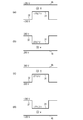
- FIG. 4 Schematic configuration diagram of a developing device and the like according to Embodiment 4 Schematic diagram of electric potential of conductor part 32, dielectric part 31, and regulating blade 4b according to the fourth embodiment. Schematic diagram of electric potential of conductor part 32, dielectric part 31, and regulating blade 4b according to the fifth embodiment. Schematic diagram of electric potential of conductor part 32, dielectric part 31, and regulating blade 4b according to the fifth embodiment. Schematic diagram of electric potential of conductor part 32, dielectric part 31, and regulating blade 4b according to Example 6
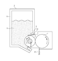
- the image forming apparatus 100 includes a photosensitive drum 1, a developing device 2, a cleaning device 8, a charging roller 7, an exposure device 91, a transfer roller 93, a fixing device 94, and the like as main components.
- the photosensitive drum 1, the developing device 2, the cleaning device 8, and the charging roller 7 are integrated as a process cartridge P, and the image forming apparatus main body (the portion of the image forming apparatus 100 excluding the process cartridge P) is integrated. It is configured to be detachable.
- the developing device 2 has a negative normal charging polarity (charging polarity for developing an electrostatic latent image. In this embodiment, since the negative electrostatic latent image is reversely developed, the normal charging polarity of the toner is negative). Contains toner with
- the exposure device 91 and the reflection mirror 92 are arranged so that the laser beam transmitted from the exposure device 91 reaches the exposure position A on the photosensitive drum 1 via the reflection mirror 92.
- a transfer roller 93 is disposed below the photosensitive drum 1.
- the transfer material S after the transfer is sent to the fixing device 94.
- a cleaning device 8 is installed downstream of the transfer position in the moving direction of the photosensitive drum.
- An attached blade is disposed so as to scrape off the toner on the photosensitive drum 1.
- the controller unit 70 comprehensively controls the following image forming operations according to a predetermined control program and reference table.
- the charging roller 7 charges the surface of the photosensitive drum 1 rotating at 100 mm / sec in the direction of the arrow R1 to a predetermined potential.
- an electrostatic latent image is formed on the photosensitive drum 1 by a laser beam transmitted from the exposure device 91 according to the image signal.
- the formed electrostatic latent image is developed by the developing device 2 at the development position C to form a toner image.
- the toner image formed on the photosensitive drum 1 is transferred to the transfer material S at the transfer position B.
- the transfer material S as a recording medium to which the toner image is transferred is sent to the fixing device 94.
- the fixing device 94 pressurizes and heats the toner image on the transfer material S to fix the toner image on the transfer material S to obtain a final image.
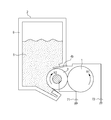
- FIG. 2 is a schematic configuration diagram of the developing device 2 and the like according to the present embodiment.
- the photosensitive drum 1 as an image carrier has an outer diameter of 24 mm and is driven to rotate in the direction of arrow R1 at a peripheral speed of 150 mm / sec.
- a developing device 2 is disposed on the left side of the photosensitive drum 1.
- the developing device 2 of the present embodiment includes a developing container 6, a developing roller 3, and a regulating blade 4, as shown in FIG.
- the developing container 6 stores toner 5 that is a non-magnetic one-component developer.
- the developing roller 3 as a toner carrier has an outer diameter of 12 mm and is driven to rotate in the direction of arrow R2 at a peripheral speed of 180 mm / sec.
- the developing roller 3 is disposed in contact with the surface of the photosensitive drum 1.
- the regulating blade 4 functions as a regulating unit that regulates the toner layer thickness on the developing roller.
- the regulation blade 4 includes a charging layer 41, a charge applying unit that applies a predetermined charge to the dielectric portion on the developing roller 3 via the toner 5, and a toner charging unit that applies a predetermined charge to the toner 5. As a function.
- the present invention has a configuration in which the toner supply member in contact with the developing roller 3 is omitted, and the above-described gradient force is used to carry a multilayer toner on the surface of the developing roller 3. Therefore, a dielectric portion and a conductor portion are provided on the surface of the developing roller 3, and the regulating blade 4 is rubbed through the toner to charge the dielectric portion, and a minute closed electric field is formed on a portion adjacent to the conductor portion. Form.
- the toner conveyed to the surface of the developing roller 3 receives a gradient force due to a minute closed electric field, and is sucked and carried on the surface of the developer carrying member.
- the surface of the developing roller 3 is configured such that a dielectric portion capable of holding electric charge and a conductor portion adjacent to the dielectric portion are exposed in a minute area.
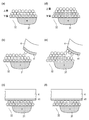
- the developing roller 3 is configured to have an elastic layer 30b made of a conductive rubber material and a surface layer 30c on the outer periphery of the shaft core 30a.
- the developing roller 3 can be manufactured by forming a surface layer 30c made of a conductive resin material in which dielectric particles are dispersed on the elastic layer 30b by, for example, coating and polishing the surface.
- 3B is a plan view of the developing roller 3
- FIG. 3C is a cross-sectional view thereof.
- the size of the dielectric part 31 is preferably about 5 to 500 ⁇ m in outer diameter. This is an optimum value for holding charges on the surface and suppressing image unevenness.
- the outer diameter is greater than 5 ⁇ m, a sufficient charge can be retained on the surface of the dielectric portion 31 and a sufficiently small closed electric field can be formed.
- the outer diameter is smaller than 500 ⁇ m, the potential difference between the dielectric portion 31 and the conductor portion 32 does not become too large, and image unevenness can be suppressed.
- the dielectric portion 31 passes through the toner layer thickness regulation position by the regulation blade 4 and then passes through the toner layer thickness regulation position (during the rotation period T of the developing roller 3). Therefore, it is necessary to maintain a small electric field difference to some extent.
- the electric resistance value R and the electrostatic capacity C of the dielectric portion 31 satisfy CR ⁇ T / Ln10 (Ln: natural logarithm) with respect to the rotation period T of the developing roller 3.
- the dielectric part 31 charged at the toner layer thickness regulating position by the regulating blade 4 can maintain a charge amount of at least 10% after the rotation period T elapses.
- CR ⁇ 0.091 satisfies the above relationship and maintains a minute closed electric field.
- the electric resistance value R and the electrostatic capacitance C of the conductor portion 32 satisfy CR ⁇ T / Ln100 (Ln: natural logarithm) with respect to the rotation period T of the developing roller 3, for example.
- CR ⁇ 0.045 is satisfied so that the above relationship is satisfied and a minute closed electric field is formed.
- the volume resistivity of the dielectric particles was measured in a 23 ° C./50% RH environment by using a resistance measuring device “Hiresta-UP” manufactured by Mitsubishi Chemical Corporation and applying a voltage of 1000 V to the measurement target sample for 30 seconds. .
- the amount of the sample to be measured is preferably adjusted appropriately in consideration of the density of the particles to be measured. For example, when measuring acrylic resin particles, 0.6 g is used, and 2000 kgf / A sample to be measured was compressed by applying a pressure of cm 2 .
- the relative dielectric constant of the dielectric particles is measured as follows. First, a powder sample is put in a cylinder with a bottom area of 2.26 cm 2 and 15 kg of pressure is applied to the upper and lower electrodes.
- the CR measurement of the dielectric portion 31 on the surface of the developing roller 3 can be substituted by charging the dielectric portion 31 by a predetermined method and measuring the attenuation rate. For example, a measurement sample having a surface of 1 cm ⁇ 1 cm and a thickness of 3 mm is cut out from the developing roller 3, and + ions are emitted by a zero stat 3 manufactured by MILTY. Then, the potential of the dielectric portion 31 can be measured at a predetermined time interval in the KFM mode of a scanning probe microscope (SPA300, manufactured by SII Nanotechnology Co., Ltd.), and CR can be calculated from the potential decay rate.
- SPA300 scanning probe microscope
- acrylic resin particles are dispersed in a urethane resin as a binder.
- a conductive material used for imparting conductivity to the surface layer 30c carbon black or an ion conductive material can be used in the same manner.
- the urethane resin part functions as the conductor part 32 by setting the content of the conductive material of the surface layer 30c to 0.20 part by mass with respect to 100 parts by mass of the urethane resin.
- the dielectric part 31 is made of acrylic resin particles having an average particle diameter of 30 ⁇ m.
- the average particle diameter is 20 ° C., 0.01 mass% solid content concentration, 50% cumulative particle diameter value (d50) and 90% cumulative particle diameter value measured by DLS, particularly the microtrack method
- the content ratio of the acrylic resin particles is 70 parts by mass with respect to 100 parts by mass of the urethane resin, thereby obtaining the area ratio of the dielectric part / conductor part. In this case, the area of the dielectric portion is about 50% of the whole.
- the developing system in this embodiment uses the relationship between the dielectric portion 31 on the surface of the developing roller 3, the charging layer 41 of the regulating blade 4, and the work function of the toner.
- the work function of the material used for the dielectric portion on the surface of the developing roller 3 was 5.7 eV when measured using a surface analyzer (AC-2 type, manufactured by Riken Keiki Co., Ltd.) with an irradiation light amount of 250 nW.
- the regulating blade 4 in the present example was provided with a charging layer 41a.
- the above polyamide resin is laminated on a phosphor bronze metal sheet.
- the thickness of the phosphor bronze metal sheet was 0.1 mm
- the thickness of the polyamide resin was 0.1 mm.
- the work function of the charging layer 41 was 5.42 eV by the above-described measuring method.
- toner 5 in this example a negatively charged toner using a nonmagnetic styrene acrylic type + polyester type resin was used.
- the work function of Toner 5 was 6.01 eV by the measurement method described above.
- a DC voltage of ⁇ 300 V is applied from the DC power supply 61 to the developing roller 3 as a developing bias for contact development, and the photosensitive drum 1 is set to ⁇ 500 V for the solid white image portion and ⁇ 100 V for the solid image portion.
- the latent image was designed so that In this embodiment, in order to obtain a suitable image density, the toner coat amount on the photosensitive drum 1 at the time of solid image formation requires 0.54 mg / cm 2, so that the toner coat amount on the developing roller 3 is 0.45 mg / cm 2. Cost.
- FIG. 4 solid image formation
- FIG. 5 solid white image formation
- all the toner on the developing roller 3 is used for development for solid image formation.
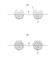
- the white toner of the toner 5 shown in FIGS. 4 and 5 is an uncharged or low-charged toner
- the minus ( ⁇ )-labeled toner is a charged toner regulated by the surface of the developing roller 3 and the charged layer 41.
- a toner coat amount of about two layers can be obtained. That is, when the solid image is formed and the solid white image is formed, the amount of toner coating after passing through the restriction position is made equal, so that the occurrence of the ghost image described above can be suppressed. (Details will be described later)
- the white toner of the toner 5 shown in FIGS. 6 and 7 is an uncharged or low-charged toner, and the toner indicated by ⁇ (minus) is charged by the surface of the developing roller 3 and the charged layer 41, and the developing roller 3. This is a toner whose surface is rolled and charged.
- FIGS. 6A, 6B, and 6C a mechanism in which toner adheres to the surface of the developing roller 3 during solid image formation, and a solid white image formation in FIGS. 6D, 6E, and 6F.
- the toner adhesion mechanism will be described.
- the surface of the developing roller 3 returns to the developing container 6 without the toner coat as shown in FIG.
- the uncharged or low-charged toner is attracted to the surface of the dielectric portion 31 where the minute closed electric field E is generated by a gradient force, and the toner that contacts the surface of the developing roller 3 is ⁇ Is charged.
- the adhered toner forms irregularities on the roller surface as shown in FIG.
- FIGS. 7A, 7B, and 7C a mechanism for regulating the toner layer on the surface of the developing roller 3 by the regulating blade 4 during solid image formation is shown in FIGS. 7D, 7E, and 7F.
- a mechanism for regulating the toner layer when forming a solid white image will be described.
- a toner layer of about four layers is formed on the surface of the developing roller 3 to be regulated.
- the minus toner on the surface of the developing roller 3 is easily peeled off from the surface of the developing roller 3 by the electric field between the charging layer 41 and the dielectric portion 31. At this time, the amount of toner that is peeled off by the electric field is larger because minus toner is laminated on the upper layer as compared with the case of solid image formation.
- the toner coating amount after passing through the regulation position at the time of solid image formation is made equal by the toner adhesion mechanism on the surface of the developing roller 3 and the toner layer regulation mechanism described above.
- ghost image generation can be greatly improved.
- the details of the comparison between the solid image formation and the solid white image formation in which the difference in the toner coat state on the surface of the developing roller 3 is most likely to appear are described.
- the subsequent toner coat amount can be made equal.
- the A4 size of 1000 sheets was formed by the image forming apparatus of FIG. 1 of the present embodiment, a favorable image was obtained while maintaining a suitable image density and without causing image defects.
- the image forming apparatus includes the developing roller 3 in which the dielectric portions 31 are scattered on the surface, and the dielectric portion 31 has the same regular charging polarity of toner as the regulation blade 4 in the charging series.
- Each member is configured to be positioned on the polar side. Accordingly, it is possible to provide an image forming apparatus that suppresses a decrease in density at the rear end of the solid image and suppresses the occurrence of ghosts using the developing device that does not include the developer supply member.
- the developing roller 3, the regulating blade 4, and the toner 5 have the above-described material configurations, but the dielectric portion is positioned on the same polarity side as the regular charging polarity of the toner with respect to the regulating blade 4 in the charging series. What is necessary is just to do and is not restricted to the above-mentioned material amount composition.
- each material is composed of ( ⁇ ) charged layer 41 ⁇ dielectric portion 31 ⁇ toner 5 (+), and the potentials of the conductor portion 32, the dielectric portion 31, and the charged layer 41 are configured. The relationship can be as shown in FIG.
- the conductivity of the charging layer 41 can obtain the effect of the present invention in both cases of conduction and insulation, but it prevents the charge on the elastic blade from being charged up and prevents the toner from having an unnecessary charge. Is preferably conductive.
- the tip surface of the regulating blade 4 is arranged so as to face the normal direction with respect to the developing roller 3 so that the effect of the present invention can be further extracted. That is, the guide blade 4 p that guides the toner to the outside of the facing area X between the control blade 4 and the developing roller 3 is provided at the tip of the control blade 4. The guide portion 4p is positioned on the side opposite to the normal charging polarity of the toner from the dielectric portion 31 on the charging series. As a result, as shown in FIG.
- the upper layer minus toner peeled off by the electric field adheres to the charging layer 41 of the guide portion 4p, and is pushed up by the minus toner conveyed one after another to the direction of the arrow. To be guided to. For this reason, the minus toner peeled off by the electric field does not stay in the vicinity of the regulation position, and the upper layer minus toner on the surface of the developing roller 3 is more reliably peeled off. Therefore, the ghost improvement effect of the present invention can be further enhanced.
- the developing roller 3 in this embodiment uses a configuration in which the dielectric portions 31 are scattered on the surface.
- “scattering” is not limited to the state where the dielectric portions are separated from each other, but is used to include the state where the dielectric portions are continuous as shown in FIG. 10A, for example. . That is, the dielectric part 31 should just be distributed regularly or irregularly in a certain ratio with respect to the whole surface, without solidifying in one place.
- the dielectric portion 31 corresponds to the sea in the sea-island type
- the conductor portion 32 corresponds to the island in the sea-island type.
- the conductor portion 32 is in contact with the lower conductive layer.
- a minute closed electric field is formed as shown by the electric lines of force E in FIG. The same effect as can be achieved.
- the photosensitive drum 1 and the developing roller 3 are arranged in contact with each other.
- the photosensitive drum 1 and the developing roller 3a are arranged in a non-contact manner as shown in FIG. May be.
- the knurled developing roller 3a shown in FIG. 12 it is easy to control the size and area ratio of the dielectric portion / conductor portion.
- an insulating resin for example, is coated. Then, the surface can be cut to expose the cored bar portion as the conductor portion 32 and the resin in the groove as the dielectric portion 31, respectively.
- FIG. 12A is a plan view of the developing roller 3a, and FIG.
- the aforementioned acrylic resin is used for the dielectric particles.
- an elastic blade 4a provided with a charging layer 41a is used as the regulating member.
- development is performed by applying a bias in which an AC bias and a DC bias are superimposed as a development bias from the power source 62.
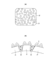
- the image forming apparatus described in the first embodiment has a configuration in which a convex portion is provided on the surface of the developing roller 3 and a dielectric portion 31 is present on the convex portion, as shown in FIG. .
- the tip surface of the regulating blade 4 is arranged so as to face the normal direction with respect to the developing roller 3 so that the unevenness on the surface of the developing roller 3 can be easily followed.
- Other main configurations are the same as those in the first embodiment.
- the dielectric portion 31 by providing the dielectric portion 31 on the convex portion, the dielectric portion 31 can be directly triboelectrically charged to the charging layer 41, and the dielectric portion 31 is charged to-of the same polarity as the toner. Can do.
- the developing roller 3 in this embodiment is configured to have an elastic layer 30b made of a conductive rubber material and a surface layer 30c on the outer periphery of the shaft core 30a.
- FIG. 13B is a plan view of the developing roller 3
- FIG. 13C is a cross-sectional view.
- the surface layer 30c is a sea-island type phase composed of a domain phase containing a polyester copolymer resin consisting of chemical formulas (A) and (B) and a matrix phase of a polyester melamine resin containing chemical formulas (A), (B) and (C). It has a separation structure.
- R 1 is a linear alkylene group having 2 to 9 carbon atoms or a branched alkylene group having 6 to 9 carbon atoms
- R 2 is a linear alkylene group having 2 to 8 carbon atoms. It is a group.
- the surface layer is characterized in that a domain phase composed of a dielectric portion and a matrix phase composed of a conductor portion in which conductive fine particles are unevenly distributed are exposed in a minute area, and the domain phase functions as the dielectric portion 31b.
- the matrix phase functions as the conductor portion 32b.
- the equivalent circle diameter of the dielectric portion 31b is preferably 10 ⁇ m or more. By setting the thickness to 10 ⁇ m or more, it is possible to obtain a charging potential amount sufficient to hold the toner.
- the equivalent circle diameter refers to the diameter of a circle having the same area as the area of the domain phase projected onto the surface of the developing roller.
- the domain phase in the present invention can be identified by a scanning electron microscope (SEM), a scanning transmission electron microscope (STEM), or the like. The area ratio of both parts is such that the area of the dielectric part is about 50% of the whole.
- the thickness of the surface layer 30c is 10 ⁇ m. Further, the surface roughness of the developing roller 3 having a convex dielectric portion can be controlled by controlling the phase separation structure.
- a method of forming a coating film having a sea-island type phase separation structure there is a method of forming a coating film by dissolving a resin material having high crystallinity and a solid state in a supersaturated amount of solvent at room temperature.
- a resin material with high crystallinity exhibits the property that crystals are likely to precipitate partially due to volatilization of the solvent during coating film formation.
- the crystal-like precipitation portion becomes the domain portion, and the portion where the coating film is continuously formed becomes the matrix portion, thereby forming a sea-island type phase separation structure.
- This domain phase that is, crystal precipitation, depends on the crystallinity of the polyester copolymer resin in this embodiment.
- control of the crystal size and the coverage is important to control the crystal size and the coverage by optimizing the molecular structure of the crystallinity of the polyester copolymer resin.
- control of the phase separation structure that is, the size of the domain, can be achieved by the boiling point, evaporation rate, and SP value of the solvent.
- the uneven distribution of the conductive fine particles in the matrix phase was confirmed by performing mapping analysis with a scanning probe microscope (SPM).
- SPM scanning probe microscope
- the domain-like region showed insulation, while the surrounding matrix region was confirmed to be conductive.
- the work function of the material used for the dielectric portion on the surface of the developing roller 3 was 5.6 eV when measured using a surface analyzer (AC-2 type, manufactured by Riken Keiki Co., Ltd.) with an irradiation light amount of 250 nW. It was.
- the dielectric portion 31b when the toner particle size is smaller than the height of the convex portion of the dielectric portion 31b, the dielectric portion 31b is negatively charged by friction with the charging layer 41. To do. As shown in FIG. 14B, when the toner particle diameter is larger than the height of the convex portion of the dielectric portion 31b, the dielectric portion 31b does not rub against the charging layer 41, but is positively charged by friction with the toner. .
- the ghost image improvement mechanism in this embodiment will be described.
- the difference from the first embodiment is that the dielectric portion 31 is present on the convex portion, and can have both positive and negative polarities depending on the relationship between the height of the convex portion and the toner particle size.
- the toner suction to the surface of the developing roller 3 in the present invention is a gradient force due to a minute closed electric field, so the direction of the force received by the toner does not depend on the direction of the electric field, and Receive force in the direction of increasing.
- the case where the dielectric 31 is negative will be described in detail in Example 3. Therefore, the mechanism for improving the ghost image is the same as that in the first embodiment, and a detailed description thereof is omitted.
- FIGS. 15A, 15B, and 15C are explanatory views showing that toner adheres to the surface of the developing roller 3 when a solid image is formed.
- FIGS. 15D, 15E, and 15F when a solid white image is formed.
- the toner adhesion explanatory drawing is shown.
- 16A, 16B, and 16C are explanatory diagrams for regulating the toner layer on the surface of the developing roller 3 during solid image formation by the regulating blade 4, and in FIGS. 16D, 16E, and 16F, FIG. 6 is an explanatory diagram of toner layer regulation during solid white image formation.
- Table 1 shows the relationship between the average toner particle diameter r, the developing roller 3 surface roughness Rzjis (ten-point average roughness), and ghost / fogging when an image of A4 size 10000 sheets is formed using the developing device of this embodiment. Shown in
- the occurrence of ghost when the surface Rzjis of the developing roller 3 is small is because a minute closed electric field cannot be formed due to friction between the dielectric portion 31b and the toner due to toner fusion to the dielectric portion 31.
- the surface Rzjis of the developing roller 3 is increased, the dielectric portion 31b is charged with the same polarity as the toner due to friction with the charging layer 41, so that the occurrence of toner fusion can be suppressed.
- Rzjis increases, the proportion of the dielectric portion 31b charged to the same polarity as the toner increases, and by setting Rzjis ⁇ r (toner average particle diameter), toner fusion can be significantly suppressed.
- the ratio of the dielectric portion 31b charged to the same polarity as the toner is determined by Rzjis and the particle size distribution of the toner.
- the reason why fog occurs when Rzjis> 3r is that three toner layers are easily formed on the unevenness of the surface of the developing roller 3, and the toner and the layer sandwiched between the toners cannot be charged. Therefore, in order to suppress fogging, it is desirable to satisfy Rzjis ⁇ 3r.
- the image forming apparatus includes the developing roller 3 in which the dielectric portions 31 are scattered on the surface, and the dielectric portion 31 has the same regular charging polarity of toner as the regulation blade 4 in the charging series.
- Each member is configured to be positioned on the polar side. Accordingly, it is possible to provide an image forming apparatus capable of realizing a long life by suppressing a decrease in density at the rear end of a solid image and suppressing generation of a ghost by using a developing device without a developer supply member. it can.
- the above-described method is adopted for forming the surface roughness of the developing roller 3, but the effect of the present invention can be achieved if the dielectric portion 31b is convex and a predetermined surface roughness can be obtained. It is not limited to.
- the present embodiment can be applied to a configuration in which a surface layer of a conductive resin in which insulating particles are dispersed is coated on a conductive substrate and the insulating particles are projected by polishing the surface to obtain a predetermined surface roughness. The same effect as can be achieved.
- FIG. 17 a developer in which an external additive 51 is dispersed on the surface of the toner 5 is employed in the image forming apparatus described in the first embodiment.
- an external additive 51 positioned on the opposite side of the normal charging polarity of the toner 5 from the dielectric portion 31 in the charging series is externally added to the surface of the toner 5, and the dielectric portion 31 is externally attached.
- the additive 51 is charged to the same polarity as the normal charging polarity of the toner.
- the dielectric part 31 is normally charged with toner. It is characterized by being charged to the same polarity as-.
- Other main configurations are the same as those in the first embodiment.
- titanium oxide was used as an external additive, and 0.5 parts by mass of the external additive was stirred at a high speed with respect to 100 parts by mass of the toner to prepare a developer by treating the toner surface.
- the development system in this embodiment uses the relationship between the work functions of the dielectric portion 31 on the surface of the developing roller 3, the toner 5, and the external additive 51.
- the work functions of the toner 5 and the external additive 51 were 6.01 eV and 5.41 eV according to the measurement method described above.
- the material of the toner 5 and the external additive 51 are selected so as to have the above-described work function, so that ( ⁇ ) toner 5 ⁇ dielectric portion 31 ⁇ charged layer 41 ⁇ external additive 51 in the charge series. (+).
- the work function difference between the toner 5 and the dielectric part 31 is smaller than the difference between the dielectric part 31 and the external additive 51, and the work function difference between the toner 5 and the charge layer 41 is changed between the charged layer 41 and the external additive 51. It is configured to be larger than the difference.
- the toner 5 is negatively charged and the external additive 51 is positively charged due to friction between the toner 5 and the dielectric part 31, and the dielectric part 31 has an external work function with a larger work function difference. It is negatively charged by friction with the additive 51.
- the charging layer 41 is positively charged due to the friction with the toner 5 having a larger work function difference.
- the ghost image improvement mechanism in this embodiment will be described.
- the difference from the first embodiment is that the dielectric portion 31 has a negative polarity. Since the toner suction to the surface of the developing roller 3 in the present invention is a gradient force due to a minute closed electric field, the direction of the force applied to the toner is not dependent on the direction of the electric field but receives the force in the direction of increasing the electric field. Therefore, as shown in FIGS. 18A and 18B, even if the dielectric portion 31 has the same polarity as that of the toner, the toner can be attracted if a minute closed electric field is formed.
- the mechanism by which toner adheres to the surface of the developing roller 3 during solid image formation and solid white image formation is the same as in the first embodiment.
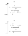
- Vdc developing bias
- the dielectric portion 31 Vdc ⁇
- Layer 41 Vdc + ⁇ .
- the ghost image generation mechanism described above can suppress the generation of ghost images by equalizing the toner coat amount after passing through the regulation position during solid image formation and solid white image formation. it can.
- Table 2 shows the results of image formation on the A4 size 10,000 sheets using the image forming apparatus of FIG. 1 for the developing device of Example 1 and the developing device of this example.
- Example 3 since the dielectric part 31 has the same polarity as the toner, the occurrence of toner fusion can be reduced and a long life can be realized.
- the image forming apparatus includes the developing roller 3 in which the dielectric portions 31 are scattered on the surface, and the dielectric portion 31 has the same regular charging polarity of toner as the regulation blade 4 in the charging series.
- Each member is configured to be positioned on the polar side. Accordingly, it is possible to provide an image forming apparatus that suppresses a decrease in density at the rear end of the solid image and suppresses the occurrence of ghosts using the developing device that does not include the developer supply member.
- the toner 5, the dielectric portion 31, and the charging layer 41 have the above-described material configurations, but are not limited thereto.
- each material is composed of ( ⁇ ) external additive 51 ⁇ charged layer 41 ⁇ dielectric portion 31 ⁇ toner 5 (+), and the conductor portion 32, dielectric portion 31,
- the potential relationship of the charging layer 41 can be as shown in FIG.
- ( ⁇ ) toner 5 ⁇ dielectric portion 31 ⁇ charge layer 41 ⁇ external additive 51 (+) in the charging series is used, but ( ⁇ ) toner 5 ⁇ dielectric portion 31 ⁇ outside.
- the additive 51 ⁇ charged layer 41 (+) may be satisfied.
- the dielectric part 31 can be charged to a negative polarity having the same polarity as the toner. The same effects as in the present embodiment can be obtained.
- titanium oxide is used as the external additive 51, but it is not particularly limited as long as it satisfies the above-mentioned position on the charging series in the following known inorganic powder. Specifically, oxides of metals such as magnesium, zinc and aluminum, composite metal oxides such as calcium titanate, metal salts such as calcium carbonate, etc. satisfying the above position on the charging series Can be used.
- an electric field that causes the toner to be peeled off from the dielectric portion 31 is formed by a blade bias.
- the developing roller 3 is connected to a DC power source 71 for applying a developing bias Vdc.
- Other main configurations are the same as those in the first embodiment.
- Vmf The potential difference (hereinafter referred to as Vmf) between the dielectric part 31 and the conductor part 32 during image formation was measured according to the following procedure.
- SPA300 scanning probe microscope
- the value measured in (2) above is 20V.
- Table 3 shows the results when an image was formed by applying a blade bias in this example.
- the potential difference (Vbr ⁇ Vdc) between the blade bias Vbr and the developing bias Vdc is set to be positive.
- an electric field is generated in the direction in which the toner moves from the surface of the developing roller 3 to the regulating blade 4b.
- the ghost image is improved by changing the potential difference (Vbr ⁇ Vdc) from minus to plus.
- the mechanism for improving the ghost image is the same as in the first embodiment, and is because the upper layer toner in FIGS. 7B and 7E is peeled off by the electric field generated by the potential difference (Vbr ⁇ Vdc).
- Vmf 21.3V
- the ghost image is significantly improved by setting the potential difference (Vbr ⁇ Vdc) to + 25V to + 50V, which is larger than Vmf.
- FIG. 21A is a schematic diagram of the potential of the conductor portion 32, the dielectric portion 31, and the regulating blade 4, which are modified examples of the present embodiment, and FIGS. Show.
- FIG. 21A shows a case where the toner is negative and the developing bias is negative.
- FIG. 21B shows the case where the toner is positive and the developing bias is positive.
- FIG. 21C shows the case where the toner is negative and the developing bias is positive.
- FIG. 21D shows a case where the toner has positive polarity and the developing bias is negative.
- the potential relationship is set such that an electric field for removing the toner from the dielectric portion 31 is generated.
- the electric potential of the conductor portion 32, the dielectric portion 31, and the regulating blade 4 were set as shown in FIG. A suitable image density was maintained, and a good image was obtained without image defects.
- the image forming apparatus includes the developing roller 3 in which the dielectric portions 31 are scattered on the surface, and the potential difference obtained by subtracting the potential of the dielectric portion 31 from the potential of the regulating blade 4b is opposite to the normal charging polarity of the toner.
- a voltage is applied to the regulating blade 4b so as to be polar. Accordingly, it is possible to provide an image forming apparatus that suppresses a decrease in density at the rear end of the solid image and suppresses the occurrence of ghosts using the developing device that does not include the developer supply member.
- Table 4 shows the results when an image was formed by applying a blade bias in this example.
- the potential difference (Vbr ⁇ Vdc) between the blade bias Vbr and the developing bias Vdc is set to be positive.
- an electric field is generated in the direction in which the toner moves from the surface of the developing roller 3 to the regulating blade 4b.
- Vmf 21.3V as in the fourth embodiment.
- the ghost image is improved by changing the potential difference (Vbr ⁇ Vdc) from minus to plus.
- the mechanism for improving the ghost image is the same as in the third embodiment, and is because the upper layer toner in FIGS. 19B and 19E is peeled off by the electric field generated by the potential difference (Vbr ⁇ Vdc).
- the dielectric part 31 is negatively charged by friction with the charging layer 41. Otherwise, the dielectric part 31 is Charges positively due to friction with toner.
- the dielectric portion 31b has a high ratio of being charged to-, but there is also a dielectric portion 31 that is charged to +.
- the potential schematic diagram in the present embodiment employs FIGS. 22A, 22B, 22C, and 22D when the dielectric portion 31b includes both the one that is charged to the same polarity as the toner and the other that are not.
- FIGS. 23A, 23B, 23C, and 23D are employed.
- the mechanism for suppressing the toner fusion to the dielectric portion 31 due to the increase in the number of formed images is the same as in the third embodiment.
- the electric potential of the conductor portion 32, the dielectric portion 31, and the regulating blade 4 were set as shown in FIG. 22A, and image formation of 10,000 sheets of A4 size was performed. A suitable image density was maintained, and a good image was obtained without image defects.
- the image forming apparatus includes the developing roller 3 in which the dielectric portions 31 are scattered on the surface, and the potential difference obtained by subtracting the potential of the dielectric portion 31 from the potential of the regulating blade 4b is opposite to the normal charging polarity of the toner.
- a voltage is applied to the regulating blade 4b so as to be polar. Accordingly, it is possible to provide an image forming apparatus capable of realizing a long life by suppressing a decrease in density at the rear end of a solid image and suppressing generation of a ghost by using a developing device without a developer supply member. it can.
- Table 5 shows the results when an image was formed by applying a blade bias in this example.
- the potential difference (Vbr ⁇ Vdc) is set so that the potential difference (Vbr ⁇ Vdc) between the blade bias Vbr and the developing bias Vdc is positive.
- Vbr ⁇ Vdc potential difference between the blade bias Vbr and the developing bias Vdc
- the ghost image is improved by changing the potential difference (Vbr ⁇ Vdc) from minus to plus.
- the mechanism for improving the ghost image is the same as in the second embodiment, and is because the upper layer toner in FIGS. 7B and 7E is peeled off by the electric field due to the potential difference (Vbr ⁇ Vdc).
- the conductor portion 32 since the dielectric portion 31 is charged with the same polarity ( ⁇ ) as that of the toner, the conductor portion 32 has a potential that is more difficult to peel off by an electric field. Therefore, by setting the potential difference (Vbr ⁇ Vdc)> 0, an electric field that peels off the toner from both the dielectric portion 31 and the conductor portion 32 can be formed, and the ghost image is greatly improved.
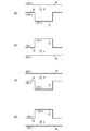
- FIG. 24A shows a potential schematic diagram of the conductor portion 32, the dielectric portion 31, and the regulating blade 4b, which are modified examples of this embodiment, and FIGS. Show. 24A shows the case where the toner has a negative polarity and the development bias is negative, FIG. 24B shows the case where the toner has a positive polarity and the development bias has a positive polarity, and FIG. 24C shows the case where the toner has a negative polarity. When the bias is positive, FIG. 24D shows the case where the toner is positive and negative and the developing bias is negative. In any case, the potential relationship is set such that an electric field for removing the toner from the dielectric portion 31 is generated.
- the mechanism for suppressing the toner fusion to the dielectric portion 31 due to the increase in the number of image formations is the same as in the second embodiment.
- the conductor part 32, the dielectric part 31, and the regulating blade 4 potential are set as shown in FIG. A good image was obtained while maintaining a high image density and without image defects.
- the image forming apparatus includes the developing roller 3 in which the dielectric portions 31 are scattered on the surface, and the potential difference obtained by subtracting the potential of the dielectric portion 31 from the potential of the regulating blade 4b is opposite to the normal charging polarity of the toner.
- a voltage is applied to the regulating blade 4b so as to be polar. Accordingly, it is possible to provide an image forming apparatus capable of realizing a long life by suppressing a decrease in density at the rear end of a solid image and suppressing generation of a ghost by using a developing device without a developer supply member. it can.
Abstract
Provided is an image formation device in which ghosting and density reduction at the trailing end of a solid image are suppressed in a development device having no developer supplying member. A developing roller (3) is provided on which dielectric parts (31) are scattered on the surface thereof, and each member is configured so that the dielectric parts (31) are positioned more on the normal-charging-polarity and same-polarity side of a toner than a regulating blade (4) in a charging series.
Description
本発明は、電子写真方式を利用した画像形成装置に用いられる現像装置に関する。
The present invention relates to a developing device used in an image forming apparatus using an electrophotographic system.
従来の画像形成装置において、画像形成の履歴が残像として後の画像形成に現れる、所謂ゴーストという現象が知られている。ゴーストは、例えば濃度の高いベタ画像形成後にハーフトーン画像を形成すると、ハーフトーン画像上にベタ画像の跡が現れやすい。また、濃度の高い所謂ベタ画像を形成する際に、画像後端の濃度が低下してしまう現象が知られている。
In a conventional image forming apparatus, a so-called ghost phenomenon in which an image formation history appears as an afterimage in later image formation is known. For example, when a halftone image is formed after a solid image having a high density is formed, a trace of the solid image tends to appear on the halftone image. Further, a phenomenon is known in which the density at the rear end of an image is lowered when a so-called solid image having a high density is formed.
このようなゴーストの発生やベタ画像後端の濃度低下を抑制するために、従来の現像装置では、現像ローラ(トナー担持体)に対して接触してトナーの供給および剥ぎ取りを行う供給ローラ(トナー供給部材)を設ける構成が一般的に採用されている。すなわち、現像ローラ上に残る画像形成の履歴を供給ローラの剥ぎ取り作用により消去することで、ゴーストを抑制することができる。また、供給ローラにより現像ローラへ新たなトナーを供給することで、ベタ画像後端の濃度低下を抑制することができる。
In order to suppress the occurrence of such ghosts and the decrease in density at the rear end of the solid image, in the conventional developing device, a supply roller (contacting with the developing roller (toner carrier)) for supplying and removing the toner ( A configuration in which a toner supply member is provided is generally employed. That is, ghosting can be suppressed by erasing the image forming history remaining on the developing roller by the peeling action of the supply roller. In addition, by supplying new toner to the developing roller with the supply roller, it is possible to suppress a decrease in density at the trailing edge of the solid image.
これに対し、現像装置の小型化及び低コスト化のため、上記の供給ローラを省いた現像装置が提案されている。
On the other hand, in order to reduce the size and cost of the developing device, a developing device that omits the supply roller has been proposed.
特許文献1、2では、トナー担持体として、その表面に誘電体部を散在させた構成を採用し、供給ローラを省いた現像装置が提案されている。即ち、トナー担持体表面の誘電体部を、トナー層厚規制部(規制部)が直接、又はトナーを介して摺擦することにより、誘電体部を帯電し、誘電体部とその周りとの間に微小閉電界を形成する。トナー担持体表面へ搬送されたトナーは、微小閉電界によるグラディエント力を受けて、トナー担持体表面に吸引され担持される。特許文献1、2においては、トナー担持体上のトナーの帯電量を安定化することを目的として、誘電体部が帯電系列上で規制部よりもトナーの正規帯電極性(静電潜像を現像するための帯電極性)と逆極性側に位置するような構成にすべきことが記載されている。例えばトナーの帯電極性が負極性の場合には、帯電系列上で(-)トナー<規制部<誘電体部(+)、となるような構成にすべきことが記載されている。
Patent Documents 1 and 2 propose a developing device that employs a configuration in which a dielectric portion is scattered on the surface of a toner carrier and omits a supply roller. That is, the dielectric layer on the surface of the toner carrying member is rubbed directly or via the toner by the toner layer thickness regulating unit (regulating unit) to charge the dielectric unit, so that the dielectric unit and its surroundings A minute closed electric field is formed between them. The toner conveyed to the surface of the toner carrier is attracted and carried on the surface of the toner carrier by receiving a gradient force due to a minute closed electric field. In Patent Documents 1 and 2, for the purpose of stabilizing the charge amount of the toner on the toner carrier, the dielectric portion is charged with a normal charging polarity of the toner (the electrostatic latent image is developed more than the regulating portion on the charging series). It is described that the structure should be located on the opposite polarity side to the charging polarity). For example, it is described that when the charging polarity of the toner is negative, the structure should be such that (−) toner <regulating portion <dielectric portion (+) on the charging series.
しかしながら、上記の従来技術のように誘電体部が帯電系列上で規制部よりもトナーの正規帯電極性と逆極性側に位置するような構成を採用すると、前述のゴーストが発生しやすくなることが本発明者の検討により明らかとなった。上記の従来技術の構成では、トナーが誘電体部に対して静電的に強く付着するためトナー層厚の規制が難しく、現像ローラ上に残る画像形成の履歴を十分に消去できない傾向がある。
However, when the configuration in which the dielectric portion is positioned on the opposite side to the normal charging polarity of the toner with respect to the regulating portion as in the conventional technique as described above, the above-described ghost is likely to occur. It became clear by examination of this inventor. In the above prior art configuration, the toner adheres electrostatically strongly to the dielectric portion, so it is difficult to regulate the thickness of the toner layer, and there is a tendency that the history of image formation remaining on the developing roller cannot be sufficiently erased.
従って本発明の目的は、トナー担持体に接触してトナーの供給および剥ぎ取りを行うトナー供給部材を省いた現像装置において、ベタ画像後端の濃度低下を抑制し、且つゴーストの発生をも抑制することである。
Accordingly, it is an object of the present invention to suppress a decrease in density at the trailing edge of a solid image and also to suppress the occurrence of a ghost in a developing device that omits a toner supply member that contacts and contacts a toner carrier. It is to be.
上記目的を達成するため、本出願に係る第一の発明は、トナーを収納する容器と、表面に散在する誘電体部を有し、前記トナーを担持するトナー担持体と、前記トナー担持体上の前記トナーの層厚を規制する規制部と、を備える現像装置において、前記誘電体部が、帯電系列上で前記規制部よりも前記トナーの正規帯電極性と同極性側に位置することを特徴とする現像装置である。
In order to achieve the above object, a first invention according to the present application includes a container for storing toner, a toner carrier having a dielectric portion scattered on the surface, and carrying the toner, and the toner carrier. And a regulating unit that regulates the layer thickness of the toner, wherein the dielectric unit is positioned on the same polarity side as the regular charging polarity of the toner with respect to the regulating unit in a charging series. The developing device.
上記目的を達成するため、本出願に係る第二の発明は、トナーを収納する容器と、表面に散在する誘電体部を有し、前記トナーを担持するトナー担持体と、前記トナー担持体上の前記トナーの層厚を規制する規制部と、を備える現像装置と、前記規制部の電位から前記誘電体部の電位を減じた電位差が前記トナーの正規帯電極性と逆極性となるように、前記規制部に電圧を印加する電圧印加装置と、を有することを特徴とする画像形成装置である。
In order to achieve the above object, a second invention according to the present application includes a container for storing toner, a toner carrier having a dielectric part scattered on the surface, and carrying the toner, and the toner carrier. And a developing device that regulates the layer thickness of the toner, and a potential difference obtained by subtracting the potential of the dielectric portion from the potential of the regulating portion is opposite to the normal charging polarity of the toner. An image forming apparatus comprising: a voltage applying device that applies a voltage to the restricting portion.
以上説明したように、本発明によれば、トナー担持体に接触してトナーの供給および剥ぎ取りを行うトナー供給部材を省いた現像装置において、ベタ画像後端の濃度低下とゴーストの発生とを抑制することができる。
As described above, according to the present invention, in the developing device that omits the toner supply member that contacts and removes the toner in contact with the toner carrying member, the density of the solid image trailing edge is reduced and the ghost is generated. Can be suppressed.
以下、本発明に係る画像形成装置を図面に則して更に詳しく説明する。以下に説明する実施例は、例示的に本発明を説明するものであって、以下に記載される構成部品の寸法、材質、形状、その相対配置などは、特に特定的な記載がない限りは、本発明の範囲をそれに限定するものではない。
Hereinafter, the image forming apparatus according to the present invention will be described in more detail with reference to the drawings. The examples described below illustrate the present invention by way of example, and the dimensions, materials, shapes, relative arrangements, etc. of the components described below are not particularly specified unless otherwise specified. However, the scope of the present invention is not limited thereto.
<画像形成装置>
本実施例の画像形成装置100の概略構成を図1に示す。本実施例の画像形成装置100は、主な構成として、感光ドラム1、現像装置2、クリーニング装置8、帯電ローラ7、露光装置91、転写ローラ93、定着器94等を有する。感光ドラム1、現像装置2、クリーニング装置8、帯電ローラ7は、プロセスカートリッジPとして一体化されており、画像形成装置本体(画像形成装置100のうち、プロセスカートリッジPを除いた部分)に対して着脱可能に構成されている。現像装置2は負の正規帯電極性(静電潜像を現像するための帯電極性。本実施例では負極性の静電潜像を反転現像するので、トナーの正規帯電極性は負である。)をもつトナーを内包している。 <Image forming apparatus>
A schematic configuration of theimage forming apparatus 100 of the present embodiment is shown in FIG. The image forming apparatus 100 according to the present exemplary embodiment includes a photosensitive drum 1, a developing device 2, a cleaning device 8, a charging roller 7, an exposure device 91, a transfer roller 93, a fixing device 94, and the like as main components. The photosensitive drum 1, the developing device 2, the cleaning device 8, and the charging roller 7 are integrated as a process cartridge P, and the image forming apparatus main body (the portion of the image forming apparatus 100 excluding the process cartridge P) is integrated. It is configured to be detachable. The developing device 2 has a negative normal charging polarity (charging polarity for developing an electrostatic latent image. In this embodiment, since the negative electrostatic latent image is reversely developed, the normal charging polarity of the toner is negative). Contains toner with
本実施例の画像形成装置100の概略構成を図1に示す。本実施例の画像形成装置100は、主な構成として、感光ドラム1、現像装置2、クリーニング装置8、帯電ローラ7、露光装置91、転写ローラ93、定着器94等を有する。感光ドラム1、現像装置2、クリーニング装置8、帯電ローラ7は、プロセスカートリッジPとして一体化されており、画像形成装置本体(画像形成装置100のうち、プロセスカートリッジPを除いた部分)に対して着脱可能に構成されている。現像装置2は負の正規帯電極性(静電潜像を現像するための帯電極性。本実施例では負極性の静電潜像を反転現像するので、トナーの正規帯電極性は負である。)をもつトナーを内包している。 <Image forming apparatus>
A schematic configuration of the
露光装置91から発信されたレーザービームが反射ミラー92を介して感光ドラム1上の露光位置Aに達するように、露光装置91、反射ミラー92は配置されている。感光ドラム1の下部には、転写ローラ93が配置されている。転写後の転写材Sは定着器94に送られる。転写位置に対して感光ドラムの移動方向下流にはクリーニング装置8が設置されている。付属のブレードが感光ドラム1上のトナーを掻き落とせるように接触配置されている。
The exposure device 91 and the reflection mirror 92 are arranged so that the laser beam transmitted from the exposure device 91 reaches the exposure position A on the photosensitive drum 1 via the reflection mirror 92. A transfer roller 93 is disposed below the photosensitive drum 1. The transfer material S after the transfer is sent to the fixing device 94. A cleaning device 8 is installed downstream of the transfer position in the moving direction of the photosensitive drum. An attached blade is disposed so as to scrape off the toner on the photosensitive drum 1.
画像形成装置の画像形成動作について説明する。コントローラ部70が所定の制御プログラムや参照テーブルに従って以下の画像形成動作を統括的に制御する。まず、矢印R1方向に100mm/secで回転している感光ドラム1の表面上を、帯電ローラ7で所定電位に帯電する。露光位置Aにおいて、画像信号に応じて露光装置91から発信されたレーザービームにより、感光ドラム1上に静電潜像を形成する。形成した静電潜像を現像位置Cにおいて現像装置2で現像し、トナー像を形成する。感光ドラム1上に形成されたトナー像は、転写位置Bにて転写材Sに転写される。トナー像を転写された記録媒体としての転写材Sは定着器94に送られる。定着器94は転写材S上のトナー像を加圧及び加熱して転写材Sに定着し、最終画像とする。
The image forming operation of the image forming apparatus will be described. The controller unit 70 comprehensively controls the following image forming operations according to a predetermined control program and reference table. First, the charging roller 7 charges the surface of the photosensitive drum 1 rotating at 100 mm / sec in the direction of the arrow R1 to a predetermined potential. At the exposure position A, an electrostatic latent image is formed on the photosensitive drum 1 by a laser beam transmitted from the exposure device 91 according to the image signal. The formed electrostatic latent image is developed by the developing device 2 at the development position C to form a toner image. The toner image formed on the photosensitive drum 1 is transferred to the transfer material S at the transfer position B. The transfer material S as a recording medium to which the toner image is transferred is sent to the fixing device 94. The fixing device 94 pressurizes and heats the toner image on the transfer material S to fix the toner image on the transfer material S to obtain a final image.
次に、本実施例の現像装置の構成について説明する。
図2は、本実施例に係る現像装置2等の概略構成図である。像担持体としての感光体ドラム1は外径24mmであり、周速150mm/secで、矢印R1方向に回転駆動される。感光体ドラム1の左側に現像装置2が配設されている。感光体ドラム1の周囲には、電子写真プロセスを実施するために、周知の帯電手段、露光手段、転写手段、クリーニング手段、定着装置(いずれも不図示)等が配設されている。 Next, the configuration of the developing device of this embodiment will be described.
FIG. 2 is a schematic configuration diagram of the developingdevice 2 and the like according to the present embodiment. The photosensitive drum 1 as an image carrier has an outer diameter of 24 mm and is driven to rotate in the direction of arrow R1 at a peripheral speed of 150 mm / sec. A developing device 2 is disposed on the left side of the photosensitive drum 1. Around the photosensitive drum 1, a known charging unit, exposure unit, transfer unit, cleaning unit, fixing device (all not shown) and the like are disposed in order to perform the electrophotographic process.
図2は、本実施例に係る現像装置2等の概略構成図である。像担持体としての感光体ドラム1は外径24mmであり、周速150mm/secで、矢印R1方向に回転駆動される。感光体ドラム1の左側に現像装置2が配設されている。感光体ドラム1の周囲には、電子写真プロセスを実施するために、周知の帯電手段、露光手段、転写手段、クリーニング手段、定着装置(いずれも不図示)等が配設されている。 Next, the configuration of the developing device of this embodiment will be described.
FIG. 2 is a schematic configuration diagram of the developing
本実施例の現像装置2は、図2に示すように、現像容器6、現像ローラ3、規制ブレード4を備える。現像容器6は、非磁性一成分系現像剤であるトナー5を収納する。トナー担持体としての現像ローラ3は外径12mmであり、周速180mm/secで矢印R2方向に回転駆動される。本実施例では、現像ローラ3は感光ドラム1表面に接触配置している。また、規制ブレード4は、現像ローラ上のトナーの層厚を規制する規制部として機能する。また、規制ブレード4は、帯電層41を備え、現像ローラ3上の誘電体部にトナー5を介して所定の電荷を付与する電荷付与手段、及びトナー5に所定の電荷を付与するトナー帯電手段としての機能を有している。
The developing device 2 of the present embodiment includes a developing container 6, a developing roller 3, and a regulating blade 4, as shown in FIG. The developing container 6 stores toner 5 that is a non-magnetic one-component developer. The developing roller 3 as a toner carrier has an outer diameter of 12 mm and is driven to rotate in the direction of arrow R2 at a peripheral speed of 180 mm / sec. In this embodiment, the developing roller 3 is disposed in contact with the surface of the photosensitive drum 1. The regulating blade 4 functions as a regulating unit that regulates the toner layer thickness on the developing roller. Further, the regulation blade 4 includes a charging layer 41, a charge applying unit that applies a predetermined charge to the dielectric portion on the developing roller 3 via the toner 5, and a toner charging unit that applies a predetermined charge to the toner 5. As a function.
本発明は現像ローラ3に当接するトナー供給部材を省いた構成であり、現像ローラ3表面に多層のトナーを担持するため、前述のグラディエント力を利用している。そのため現像ローラ3表面に誘電体部と導電体部を設け、規制ブレード4がトナーを介して摺擦することにより、誘電体部を帯電し、導電体部との隣接部上に微小閉電界を形成する。現像ローラ3表面へ搬送されたトナーは、微小閉電界によるグラディエント力を受けて、現像剤担持体表面に吸引され担持される。
The present invention has a configuration in which the toner supply member in contact with the developing roller 3 is omitted, and the above-described gradient force is used to carry a multilayer toner on the surface of the developing roller 3. Therefore, a dielectric portion and a conductor portion are provided on the surface of the developing roller 3, and the regulating blade 4 is rubbed through the toner to charge the dielectric portion, and a minute closed electric field is formed on a portion adjacent to the conductor portion. Form. The toner conveyed to the surface of the developing roller 3 receives a gradient force due to a minute closed electric field, and is sucked and carried on the surface of the developer carrying member.
本実施例における現像ローラ3の表面は、電荷を保持できる誘電体部と、誘電体部に隣接する導電体部とが微小面積で混在露出するように構成されている。具体的には、図3(a)に示すように軸芯体30aの外周上に、導電性ゴム材料からなる弾性層30bと、表面層30cとを有して現像ローラ3が構成される。現像ローラ3は、弾性層30b上に、誘電体粒子を分散した導電性樹脂材料からなる表面層30cを例えばコーティング等で形成して、その表面を研磨して作製することができる。現像ローラ3の平面図を図3(b)、断面図を図3(c)に示す。誘電体部31を所定の方法にて帯電することにより、図3(c)の電気力線Eで示すように微小閉電界(マイクロフィールド)が形成される。
In the present embodiment, the surface of the developing roller 3 is configured such that a dielectric portion capable of holding electric charge and a conductor portion adjacent to the dielectric portion are exposed in a minute area. Specifically, as shown in FIG. 3A, the developing roller 3 is configured to have an elastic layer 30b made of a conductive rubber material and a surface layer 30c on the outer periphery of the shaft core 30a. The developing roller 3 can be manufactured by forming a surface layer 30c made of a conductive resin material in which dielectric particles are dispersed on the elastic layer 30b by, for example, coating and polishing the surface. 3B is a plan view of the developing roller 3, and FIG. 3C is a cross-sectional view thereof. By charging the dielectric portion 31 by a predetermined method, a minute closed electric field (microfield) is formed as indicated by the electric lines of force E in FIG.
誘電体部31の大きさは、外径が5~500μm程度にすることが望ましい。これは、表面に電荷を保持し、画像ムラを抑制するために最適な値である。外径>5μmである場合には、誘電体部31表面に十分な電荷を保持し、十分な微小閉電界を形成することができる。また、外径<500μmとである場合には、誘電体部31と導電体部32の電位差が大きくなり過ぎず、画像のムラを抑制することができる。更に、誘電体部31は、規制ブレード4によるトナー層厚規位置を通過してから次にトナー層厚規制位置を通過するまでの間(現像ローラ3の回転周期Tの間)、導電部32との電位差をある程度維持し、微小閉電界を維持する必要がある。そのため、誘電体部31の電気抵抗値R、静電容量Cは、現像ローラ3の回転周期Tに対して、CR≧T/Ln10(Ln:自然対数)を満たすことが好ましい。これにより、規制ブレード4によるトナー層厚規制位置で帯電された誘電体部31は、回転周期T経過後、少なくとも10%以上の電荷量を維持することができる。本実施例ではCR≧0.091とすることで上述の関係を満たし、微小閉電界を維持している。
The size of the dielectric part 31 is preferably about 5 to 500 μm in outer diameter. This is an optimum value for holding charges on the surface and suppressing image unevenness. When the outer diameter is greater than 5 μm, a sufficient charge can be retained on the surface of the dielectric portion 31 and a sufficiently small closed electric field can be formed. When the outer diameter is smaller than 500 μm, the potential difference between the dielectric portion 31 and the conductor portion 32 does not become too large, and image unevenness can be suppressed. In addition, the dielectric portion 31 passes through the toner layer thickness regulation position by the regulation blade 4 and then passes through the toner layer thickness regulation position (during the rotation period T of the developing roller 3). Therefore, it is necessary to maintain a small electric field difference to some extent. Therefore, it is preferable that the electric resistance value R and the electrostatic capacity C of the dielectric portion 31 satisfy CR ≧ T / Ln10 (Ln: natural logarithm) with respect to the rotation period T of the developing roller 3. Thereby, the dielectric part 31 charged at the toner layer thickness regulating position by the regulating blade 4 can maintain a charge amount of at least 10% after the rotation period T elapses. In the present embodiment, CR ≧ 0.091 satisfies the above relationship and maintains a minute closed electric field.
また、図3(c)の電気力線Eで示す微小閉電界を形成するためには、導電体部32が保持する電荷は小さい方が望ましい。そのため、導電体部32の電気抵抗値R、静電容量Cは、例えば現像ローラ3の回転周期Tに対して、CR<T/Ln100(Ln:自然対数)を満たすことが好ましい。これにより、導電体部31が帯電する材料であったとしても、回転周期T経過後、1%未満の電荷量へと減衰する。本実施例ではCR<0.045とすることで上述の関係を満たし、微小閉電界を形成している。
Further, in order to form the minute closed electric field indicated by the electric lines of force E in FIG. 3C, it is desirable that the electric charge held by the conductor portion 32 is small. Therefore, it is preferable that the electric resistance value R and the electrostatic capacitance C of the conductor portion 32 satisfy CR <T / Ln100 (Ln: natural logarithm) with respect to the rotation period T of the developing roller 3, for example. As a result, even if the conductor portion 31 is a charged material, it attenuates to a charge amount of less than 1% after the rotation period T has elapsed. In the present embodiment, CR <0.045 is satisfied so that the above relationship is satisfied and a minute closed electric field is formed.
誘電体粒子の体積抵抗率は、23℃/50%RH環境下で、三菱化学(株)製の抵抗測定装置Hiresta-UPを用い、測定対象試料に1000Vの電圧を30秒間印加して測定した。測定対象試料の使用量は、測定対象の粒子の密度等を考慮して適宜調整することが好ましく、例えば、アクリル樹脂粒子を測定する場合は、それを0.6g用い、そして、これらに2000kgf/cm2の圧力をかけて圧縮したものを測定対象試料とした。誘電体粒子の比誘電率は、次のようにして測定する。まず、底面積2.26cm2の円筒内に粉体試料を入れ、上下電極に15kgの加圧を行う。同時に、1Vpp、1MHzの交流電圧を印加し、そのときの電流を測定し、その後正規化して比誘電率を算出する。現像ローラ3表面の誘電体部31のCR測定は、誘電体部31を所定の方法で帯電し、その減衰率を測定することで代用できる。例えば、現像ローラ3から表面1cm×1cm、厚み3mmの測定用サンプルを切り出し、MILTY社製ゼロスタット3により+イオンを放射する。そして、誘電体部31の電位を走査型プローブ顕微鏡(SPA300,SIIナノテクノロジー(株)製)のKFMモードにて、所定時間間隔で測定し電位減衰率からCRを算出することができる。
The volume resistivity of the dielectric particles was measured in a 23 ° C./50% RH environment by using a resistance measuring device “Hiresta-UP” manufactured by Mitsubishi Chemical Corporation and applying a voltage of 1000 V to the measurement target sample for 30 seconds. . The amount of the sample to be measured is preferably adjusted appropriately in consideration of the density of the particles to be measured. For example, when measuring acrylic resin particles, 0.6 g is used, and 2000 kgf / A sample to be measured was compressed by applying a pressure of cm 2 . The relative dielectric constant of the dielectric particles is measured as follows. First, a powder sample is put in a cylinder with a bottom area of 2.26 cm 2 and 15 kg of pressure is applied to the upper and lower electrodes. At the same time, an alternating voltage of 1 Vpp and 1 MHz is applied, the current at that time is measured, and then normalized to calculate the relative dielectric constant. The CR measurement of the dielectric portion 31 on the surface of the developing roller 3 can be substituted by charging the dielectric portion 31 by a predetermined method and measuring the attenuation rate. For example, a measurement sample having a surface of 1 cm × 1 cm and a thickness of 3 mm is cut out from the developing roller 3, and + ions are emitted by a zero stat 3 manufactured by MILTY. Then, the potential of the dielectric portion 31 can be measured at a predetermined time interval in the KFM mode of a scanning probe microscope (SPA300, manufactured by SII Nanotechnology Co., Ltd.), and CR can be calculated from the potential decay rate.
図3のような表面層30cを形成するには、例えば、バインダーとしてのウレタン樹脂にアクリル樹脂粒子を分散する。表面層30cに導電性を付与するために用いる導電性物質としては、カーボンブラックやイオン導電性物質を同様に用いることができる。本実施例では、表面層30cの導電性物質の含有量を、ウレタン樹脂100質量部に対して、0.20質量部とすることで、ウレタン樹脂部は導電体部32として機能している。また、誘電体部31には平均粒径30μmのアクリル樹脂粒子を採用している。(本明細書における平均粒径とは、20℃、0.01質量%固形分濃度で、DLS、特にマイクロトラック法で測定した50%累積粒径値(d50)及び90%累積粒径値(d90)のことを意味するものとする)本実施例では、アクリル樹脂粒子の含有量をウレタン樹脂100質量部に対して、70質量部とすることで誘電体部/導電体部の面積比としては、誘電体部の面積が全体の50%程度となるようにしている。
To form the surface layer 30c as shown in FIG. 3, for example, acrylic resin particles are dispersed in a urethane resin as a binder. As a conductive material used for imparting conductivity to the surface layer 30c, carbon black or an ion conductive material can be used in the same manner. In the present embodiment, the urethane resin part functions as the conductor part 32 by setting the content of the conductive material of the surface layer 30c to 0.20 part by mass with respect to 100 parts by mass of the urethane resin. The dielectric part 31 is made of acrylic resin particles having an average particle diameter of 30 μm. (In this specification, the average particle diameter is 20 ° C., 0.01 mass% solid content concentration, 50% cumulative particle diameter value (d50) and 90% cumulative particle diameter value measured by DLS, particularly the microtrack method ( In this embodiment, the content ratio of the acrylic resin particles is 70 parts by mass with respect to 100 parts by mass of the urethane resin, thereby obtaining the area ratio of the dielectric part / conductor part. In this case, the area of the dielectric portion is about 50% of the whole.
詳細は後述するが、本実施例での現像システムには現像ローラ3表面の誘電体部31、規制ブレード4の帯電層41、及びトナーの仕事関数の関係を利用している。現像ローラ3表面の誘電体部に用いた材料の仕事関数は、表面分析装置(AC-2型、理研計器(株)製)を用い、照射光量250nWにて測定すると5.7eVであった。
Although the details will be described later, the developing system in this embodiment uses the relationship between the dielectric portion 31 on the surface of the developing roller 3, the charging layer 41 of the regulating blade 4, and the work function of the toner. The work function of the material used for the dielectric portion on the surface of the developing roller 3 was 5.7 eV when measured using a surface analyzer (AC-2 type, manufactured by Riken Keiki Co., Ltd.) with an irradiation light amount of 250 nW.
本実施例における規制ブレード4は、帯電層41aを設けたものを用いた。具体的には、リン青銅金属薄板上に前述のポリアミド樹脂をラミネート加工したものである。本実施例ではリン青銅の金属薄板の厚みを0.1mm、ポリアミド樹脂の厚みを0.1mmとした。帯電層41の仕事関数は、前述の測定方法により5.42eVであった。
The regulating blade 4 in the present example was provided with a charging layer 41a. Specifically, the above polyamide resin is laminated on a phosphor bronze metal sheet. In this example, the thickness of the phosphor bronze metal sheet was 0.1 mm, and the thickness of the polyamide resin was 0.1 mm. The work function of the charging layer 41 was 5.42 eV by the above-described measuring method.
本実施例におけるトナー5には、非磁性スチレンアクリル系+ポリエステル系樹脂使用の負帯電トナーを用いた。トナー5の仕事関数は、前述の測定方法により6.01eVであった。
As the toner 5 in this example, a negatively charged toner using a nonmagnetic styrene acrylic type + polyester type resin was used. The work function of Toner 5 was 6.01 eV by the measurement method described above.
本実施例では、接触現像用の現像バイアスとして直流電源61から現像ローラ3に-300Vの直流電圧を印加し、感光ドラム1には、ベタ白画像部で-500V、ベタ画像部で-100Vになるように潜像設計を施した。本実施例では、好適な画像濃度を得るため、ベタ画像形成時感光ドラム1上のトナーコート量として0.54mg/cm2必要であり、そのため現像ローラ3上のトナーコート量0.45mg/cm2を要する。
In this embodiment, a DC voltage of −300 V is applied from the DC power supply 61 to the developing roller 3 as a developing bias for contact development, and the photosensitive drum 1 is set to −500 V for the solid white image portion and −100 V for the solid image portion. The latent image was designed so that In this embodiment, in order to obtain a suitable image density, the toner coat amount on the photosensitive drum 1 at the time of solid image formation requires 0.54 mg / cm 2, so that the toner coat amount on the developing roller 3 is 0.45 mg / cm 2. Cost.
本実施例では、現像ローラ3の誘電体部31、規制ブレード4の帯電層41、及びトナー5を、前述した仕事関数となるよう材料選択することで、帯電系列上(-)トナー5<誘電体部31<帯電層41(+)、となるように構成している。このような構成とすることで、トナー5と帯電層41及び誘電体部31との摩擦により、トナー5に負極性の電荷を、帯電層41及び誘電体部31に正極性の電荷を付与することができる。更に、上述の帯電系列上、トナー5と帯電層41及び誘電体部31との摩擦により、現像ローラ3表面と帯電層41表面の間にはトナー5が帯電層41に移動する電位差が生じる。
In this embodiment, by selecting materials for the dielectric portion 31 of the developing roller 3, the charging layer 41 of the regulating blade 4, and the toner 5 so as to have the above-described work function, (−) toner 5 <dielectric on the charging series. The body portion 31 <charged layer 41 (+). With this configuration, negative charge is applied to the toner 5 and positive charge is applied to the charge layer 41 and the dielectric part 31 due to friction between the toner 5 and the charge layer 41 and the dielectric part 31. be able to. Further, due to the friction between the toner 5 and the charging layer 41 and the dielectric portion 31 in the above-described charging series, a potential difference in which the toner 5 moves to the charging layer 41 is generated between the surface of the developing roller 3 and the surface of the charging layer 41.
以下、本実施例での現像システムについて、図4(ベタ画像形成)図5(ベタ白画像形成)を用い説明する。本実施例では、ベタ画像形成に現像ローラ3上の全トナーを現像に使っている。図4、図5に示すトナー5の白抜きトナーは無帯電又は低帯電のトナーで、-(マイナス)表示のトナーは現像ローラ3表面と帯電層41に規制され帯電したトナーである。
Hereinafter, the development system in this embodiment will be described with reference to FIG. 4 (solid image formation) and FIG. 5 (solid white image formation). In this embodiment, all the toner on the developing roller 3 is used for development for solid image formation. The white toner of the toner 5 shown in FIGS. 4 and 5 is an uncharged or low-charged toner, and the minus (−)-labeled toner is a charged toner regulated by the surface of the developing roller 3 and the charged layer 41.
まず、ベタ画像形成について説明する。規制位置にて、図4(a)に示すようにトナー5と帯電層41及び誘電体部31との摩擦により、トナー5に負極性の電荷を、帯電層41及び誘電体部31に正極性の電荷を付与する。これにより、誘電体部31と導電体部32の間に前述の微小閉電界が形成される。現像部にて、図4(b)に示すように、現像ローラ3上の全トナーを現像する。現像後に現像ローラ表面が現像容器6へ回収され、現像容器6内にて、図4(c)に示すように、現像ローラ3上に形成された微小閉電界によるグラディエント力で、3層程度のトナー層を形成する。そして、規制位置にて、図4(a)に示すように、ベタ画像形成時においても、常に現像ローラ3上に2層程度のトナーコート量を得て、前述のベタ画像追従不良を抑制することができる(詳細は後述)。
First, solid image formation will be described. At the restricting position, as shown in FIG. 4A, negative charge is applied to the toner 5 and positive charge is applied to the charged layer 41 and the dielectric part 31 due to friction between the toner 5 and the charged layer 41 and the dielectric part 31. Of charge. As a result, the aforementioned minute closed electric field is formed between the dielectric portion 31 and the conductor portion 32. In the developing unit, as shown in FIG. 4B, all the toner on the developing roller 3 is developed. After the development, the surface of the developing roller is collected into the developing container 6, and in the developing container 6, as shown in FIG. 4C, the gradient force due to the minute closed electric field formed on the developing roller 3 is about 3 layers. A toner layer is formed. At the restricting position, as shown in FIG. 4A, even when a solid image is formed, a toner coat amount of about two layers is always obtained on the developing roller 3 to suppress the above-described solid image following defect. (Details will be described later).
次に、ベタ白画像形成について説明する。ベタ黒画像形成時と同様に、規制位置にて誘電体部31と導電体部32の間に前述の微小閉電界が形成される。現像部にて、図5(b)に示すように、現像ローラ3上の全トナーは現像容器への回収部へ向かう。回収部から現像容器6内にて、図5(c)に示すように、現像ローラ3上に形成された微小閉電界によるグラディエント力で、4層程度のトナー層を形成する。そして、規制位置にて、図5(a)に示すように、ベタ白画像形成時においても、本発明である、現像ローラ3と帯電層41の帯電系列差を利用した規制により、現像ローラ3上に2層程度のトナーコート量を得ることができる。即ち、ベタ画像形成時、ベタ白画像形成時において、規制位置通過後のトナーコート量を同等とすることで、前述のゴースト画像の発生を抑制することができる。(詳細は後述)
Next, solid white image formation will be described. Similar to the solid black image formation, the above-described minute closed electric field is formed between the dielectric portion 31 and the conductor portion 32 at the restriction position. At the developing unit, as shown in FIG. 5B, all the toner on the developing roller 3 goes to the collecting unit for the developing container. As shown in FIG. 5C, about four toner layers are formed in the developing container 6 from the collection unit by a gradient force generated by a minute closed electric field formed on the developing roller 3. Then, at the restricting position, as shown in FIG. 5A, even when a solid white image is formed, the developing roller 3 is regulated by the restriction using the charging series difference between the developing roller 3 and the charging layer 41 according to the present invention. On the top, a toner coat amount of about two layers can be obtained. That is, when the solid image is formed and the solid white image is formed, the amount of toner coating after passing through the restriction position is made equal, so that the occurrence of the ghost image described above can be suppressed. (Details will be described later)
ここで、本発明の特徴である、ゴースト画像良化メカニズムについて図6、図7を用い詳細に説明する。図6、図7に示すトナー5の白抜きトナーは無帯電又は低帯電のトナーで、-(マイナス)表示のトナーは現像ローラ3表面と帯電層41に規制され帯電したトナー、及び現像ローラ3表面を転がり帯電したトナーである。
Here, the ghost image enhancement mechanism, which is a feature of the present invention, will be described in detail with reference to FIGS. The white toner of the toner 5 shown in FIGS. 6 and 7 is an uncharged or low-charged toner, and the toner indicated by − (minus) is charged by the surface of the developing roller 3 and the charged layer 41, and the developing roller 3. This is a toner whose surface is rolled and charged.
まず、図6(a)(b)(c)にて、ベタ画像形成時、現像ローラ3表面にトナーが付着するメカニズム、図6(d)(e)(f)にて、ベタ白画像形成時のトナー付着メカニズムについて説明する。ベタ画像形成時は、図6(a)に示すように現像ローラ3表面は、トナーコートがなくなった状態で現像容器6内に戻ってくる。そして、無帯電又は低帯電のトナーが、図6(b)に示すように、微小閉電界Eが発生する誘電体部31表面にグラディエント力で吸引され、現像ローラ3表面に接触したトナーは-に帯電する。この付着したトナーは、図6(b)に示すようにローラ表面凹凸を形成し、その隙間にトナーを担持し、図6(c)に示す3層程度のトナー層を形成する。一方ベタ白画像形成時は、現像ローラ3表面にトナーコートの-電荷が積層されるため、誘電体部31と導電体部32上のトナー層表面電位は-側にシフトし、図6(d)に示すように、微小閉電界Eを形成する。そして、無帯電又は低帯電のトナーが、図6(e)に示すように、微小閉電界Eが発生する導電体部32表面にグラディエント力で吸引され、ローラ表面凹凸を形成し、その隙間にトナーを担持し、図6(f)に示す4層程度のトナー層を形成する。
First, in FIGS. 6A, 6B, and 6C, a mechanism in which toner adheres to the surface of the developing roller 3 during solid image formation, and a solid white image formation in FIGS. 6D, 6E, and 6F. The toner adhesion mechanism will be described. At the time of solid image formation, the surface of the developing roller 3 returns to the developing container 6 without the toner coat as shown in FIG. Then, as shown in FIG. 6B, the uncharged or low-charged toner is attracted to the surface of the dielectric portion 31 where the minute closed electric field E is generated by a gradient force, and the toner that contacts the surface of the developing roller 3 is − Is charged. The adhered toner forms irregularities on the roller surface as shown in FIG. 6 (b) and carries the toner in the gaps to form a toner layer of about three layers as shown in FIG. 6 (c). On the other hand, when a solid white image is formed, since the toner charge −charge is laminated on the surface of the developing roller 3, the surface potential of the toner layer on the dielectric portion 31 and the conductor portion 32 is shifted to the − side, and FIG. ), A minute closed electric field E is formed. Then, as shown in FIG. 6E, uncharged or low-charged toner is attracted to the surface of the conductor portion 32 where the minute closed electric field E is generated by a gradient force, forming irregularities on the roller surface, and in the gaps. The toner is carried to form a toner layer of about four layers as shown in FIG.
次に、図7(a)(b)(c)にて、ベタ画像形成時、現像ローラ3表面のトナー層を規制ブレード4によって規制するメカニズム、図7(d)(e)(f)にて、ベタ白画像形成時のトナー層規制メカニズムについて説明する。ベタ画像形成時は図7(a)に示すように、現像ローラ3表面に3層程度のトナー層を形成し、図7(b)に示すようにグラディエント力による拘束が弱い上層のトナーは機械的に現像ローラ3表面から剥ぎ取られる。下層のトナーは、図7(c)に示すように、規制位置へ搬送されマイナス帯電する。一方ベタ白画像形成時は、図7(d)に示すように、現像ローラ3表面に4層程度のトナー層を形成し、規制される。ここで、本実施例では、帯電系列上(-)トナー5<誘電体部31<帯電層41(+)、となるように構成している。そのため、導電体部32、誘電体部31、帯電層41の電位関係は、図8(a)に示すように、導電体部32=現像バイアス(以下Vdc)、誘電体部31=Vdc+α、帯電層41=Vdc+βとなる(仕事関数差によりα<β)。これにより、図7(e)に示すように、現像ローラ3表面のマイナストナーは、帯電層41と誘電体部31間の電界により現像ローラ3表面から剥ぎ取られやすくなる。このとき、ベタ画像形成時と比較し、より上層にマイナストナーが積層されているため、電界により剥ぎ取られるトナー量は多くなる。
Next, in FIGS. 7A, 7B, and 7C, a mechanism for regulating the toner layer on the surface of the developing roller 3 by the regulating blade 4 during solid image formation is shown in FIGS. 7D, 7E, and 7F. A mechanism for regulating the toner layer when forming a solid white image will be described. When a solid image is formed, about three toner layers are formed on the surface of the developing roller 3 as shown in FIG. 7A. As shown in FIG. Thus, it is peeled off from the surface of the developing roller 3. As shown in FIG. 7C, the lower layer toner is conveyed to the regulation position and negatively charged. On the other hand, when a solid white image is formed, as shown in FIG. 7D, a toner layer of about four layers is formed on the surface of the developing roller 3 to be regulated. Here, in this embodiment, the configuration is such that (−) toner 5 <dielectric portion 31 <charge layer 41 (+) on the charge series. Therefore, as shown in FIG. 8A, the potential relationship among the conductor portion 32, the dielectric portion 31, and the charging layer 41 is that the conductor portion 32 = developing bias (hereinafter referred to as Vdc), the dielectric portion 31 = Vdc + α, Layer 41 = Vdc + β (α <β due to work function difference). As a result, as shown in FIG. 7E, the minus toner on the surface of the developing roller 3 is easily peeled off from the surface of the developing roller 3 by the electric field between the charging layer 41 and the dielectric portion 31. At this time, the amount of toner that is peeled off by the electric field is larger because minus toner is laminated on the upper layer as compared with the case of solid image formation.
即ち、本実施例では以上説明した、現像ローラ3表面へのトナー付着メカニズム及び、トナー層規制メカニズムにより、ベタ画像形成時ベタ白画像形成時の規制位置通過後のトナーコート量を同等とすることで、ゴースト画像発生を大幅に良化することができる。ここでは、現像ローラ3表面のトナーコート状態に最も違いが表れやすいベタ画像形成とベタ白画像形成との比較について詳細を述べたが、ハーフトーン画像形成時においても、前述のメカニズムにより規制位置通過後のトナーコート量を同等とすることができる。また、本実施例の図1の画像形成装置によりA4サイズ1000枚の画像形成を行ったが、好適な画像濃度を維持し、画像不良の発生無く、良好な画像が得られた。
That is, in this embodiment, the toner coating amount after passing through the regulation position at the time of solid image formation is made equal by the toner adhesion mechanism on the surface of the developing roller 3 and the toner layer regulation mechanism described above. Thus, ghost image generation can be greatly improved. Here, the details of the comparison between the solid image formation and the solid white image formation in which the difference in the toner coat state on the surface of the developing roller 3 is most likely to appear are described. The subsequent toner coat amount can be made equal. In addition, although the A4 size of 1000 sheets was formed by the image forming apparatus of FIG. 1 of the present embodiment, a favorable image was obtained while maintaining a suitable image density and without causing image defects.
以上のように、本実施例の画像形成装置は、表面に誘電体部31が散在する現像ローラ3を備え、誘電体部31が帯電系列上で規制ブレード4よりもトナーの正規帯電極性と同極性側に位置するように各部材が構成される。これにより、現像剤供給部材を省いた現像装置を用いて、ベタ画像後端の濃度低下を抑制し、且つゴーストの発生をも抑制する画像形成装置を提供することができる。
As described above, the image forming apparatus according to the present exemplary embodiment includes the developing roller 3 in which the dielectric portions 31 are scattered on the surface, and the dielectric portion 31 has the same regular charging polarity of toner as the regulation blade 4 in the charging series. Each member is configured to be positioned on the polar side. Accordingly, it is possible to provide an image forming apparatus that suppresses a decrease in density at the rear end of the solid image and suppresses the occurrence of ghosts using the developing device that does not include the developer supply member.
なお、本実施例では、現像ローラ3、規制ブレード4、トナー5を前述の材料構成としているが、誘電体部が帯電系列上で規制ブレード4よりもトナーの正規帯電極性と同極性側に位置すればよく、前述の材量構成に限るものではない。例えばトナーが正帯電極性である場合には(-)帯電層41<誘電体部31<トナー5(+)と各材料を構成し、導電体部32、誘電体部31、帯電層41の電位関係を、図8(b)のようにできる。
In the present embodiment, the developing roller 3, the regulating blade 4, and the toner 5 have the above-described material configurations, but the dielectric portion is positioned on the same polarity side as the regular charging polarity of the toner with respect to the regulating blade 4 in the charging series. What is necessary is just to do and is not restricted to the above-mentioned material amount composition. For example, when the toner has a positive charge polarity, each material is composed of (−) charged layer 41 <dielectric portion 31 <toner 5 (+), and the potentials of the conductor portion 32, the dielectric portion 31, and the charged layer 41 are configured. The relationship can be as shown in FIG.
帯電層41の導電性は、導電、絶縁いずれの場合でも本発明の効果を得ることができるが、弾性ブレード上の電荷のチャージアップを防止し、トナーに不必要な電荷を持たせないためには導電化することが望ましい。
The conductivity of the charging layer 41 can obtain the effect of the present invention in both cases of conduction and insulation, but it prevents the charge on the elastic blade from being charged up and prevents the toner from having an unnecessary charge. Is preferably conductive.
また、本発明の効果をより引き出すことができるように、図9(a)に示すように、規制ブレード4の先端面が現像ローラ3に対して法線方向を向くよう配置している。すなわち、規制ブレード4の先端に、トナーを規制部ブレード4と現像ローラ3との対向領域Xの外へ案内する案内部4pを有する。案内部4pは、帯電系列上で誘電体部31よりもトナーの正規帯電極性と逆極性側に位置する。これにより、図9(b)に示すように、電界により剥ぎ取られた上層のマイナストナーは、案内部4pの帯電層41に付着し、次々と搬送されてくるマイナストナーに押し上げられて矢印方向へ案内される。このため、電界により剥ぎ取られたマイナストナーは規制位置近傍に留まらず、現像ローラ3表面の上層マイナストナーはより確実に剥ぎ取られる。したがって、本発明のゴースト改善効果を一層高めることができる。
Further, as shown in FIG. 9A, the tip surface of the regulating blade 4 is arranged so as to face the normal direction with respect to the developing roller 3 so that the effect of the present invention can be further extracted. That is, the guide blade 4 p that guides the toner to the outside of the facing area X between the control blade 4 and the developing roller 3 is provided at the tip of the control blade 4. The guide portion 4p is positioned on the side opposite to the normal charging polarity of the toner from the dielectric portion 31 on the charging series. As a result, as shown in FIG. 9B, the upper layer minus toner peeled off by the electric field adheres to the charging layer 41 of the guide portion 4p, and is pushed up by the minus toner conveyed one after another to the direction of the arrow. To be guided to. For this reason, the minus toner peeled off by the electric field does not stay in the vicinity of the regulation position, and the upper layer minus toner on the surface of the developing roller 3 is more reliably peeled off. Therefore, the ghost improvement effect of the present invention can be further enhanced.
本実施例における現像ローラ3は、表面に誘電体部31が散在する構成を用いている。ここで、「散在」とは、誘電体部同士が分離している状態に限られず、例えば図10(a)に示すように、誘電体部が連続している状態も含む意味で用いている。すなわち、誘電体部31は、表面全体に対してある程度の割合で、一箇所に固まることなく、規則的に又は不規則に分布していればよい。図10(a)では、誘電体部31が海島型における海に相当し、導電体部32が海島型における島に相当する。図10(b)に示すように導電体部32は下層の導電層と接触している。このような構成においても、誘電体部31を所定の方法にて帯電することにより、図10(b)の電気力線Eで示すように微小閉電界(マイクロフィールド)が形成され、本実施例と同等の効果を奏し得る。
The developing roller 3 in this embodiment uses a configuration in which the dielectric portions 31 are scattered on the surface. Here, “scattering” is not limited to the state where the dielectric portions are separated from each other, but is used to include the state where the dielectric portions are continuous as shown in FIG. 10A, for example. . That is, the dielectric part 31 should just be distributed regularly or irregularly in a certain ratio with respect to the whole surface, without solidifying in one place. In FIG. 10A, the dielectric portion 31 corresponds to the sea in the sea-island type, and the conductor portion 32 corresponds to the island in the sea-island type. As shown in FIG. 10B, the conductor portion 32 is in contact with the lower conductive layer. Even in such a configuration, by charging the dielectric portion 31 by a predetermined method, a minute closed electric field (microfield) is formed as shown by the electric lines of force E in FIG. The same effect as can be achieved.
本実施例では、感光ドラム1と現像ローラ3を接触配置する構成としたが、接触現像時トナーへかかる圧力を無くすため、図11に示すように感光ドラム1と現像ローラ3aを非接触で配置してもよい。この場合、図12に示すローレット型現像ローラ3a採用すると、誘電体部・導電体部の大きさや面積比の制御が容易である。具体的には、芯金ローラの表面をローレット加工して所定の溝を形成した後、絶縁性の例えば樹脂をコートする。その後に表面を切削加工して芯金部が導電体部32として、溝内の樹脂が誘電体部31として、それぞれ表面に露出するようにすることによって形成できる。現像ローラ3aの平面図を図12(a)、断面図を図12(b)に示す。誘電体粒子には、前述のアクリル樹脂を使用している。規制部材には、弾性ブレード4aに帯電層41aを設けたものを用いている。図11に示す構成では、電源62から現像バイアスとして交流バイアスと直流バイアスを重畳したバイアスを印加することで現像を行う。このように非接触現像の場合であっても、現像ローラ、規制部材を上述のような構成とすることで、本実施例と同等の効果を奏し得る。
In this embodiment, the photosensitive drum 1 and the developing roller 3 are arranged in contact with each other. However, in order to eliminate the pressure applied to the toner during contact development, the photosensitive drum 1 and the developing roller 3a are arranged in a non-contact manner as shown in FIG. May be. In this case, when the knurled developing roller 3a shown in FIG. 12 is adopted, it is easy to control the size and area ratio of the dielectric portion / conductor portion. Specifically, after the surface of the cored bar roller is knurled to form a predetermined groove, an insulating resin, for example, is coated. Then, the surface can be cut to expose the cored bar portion as the conductor portion 32 and the resin in the groove as the dielectric portion 31, respectively. FIG. 12A is a plan view of the developing roller 3a, and FIG. The aforementioned acrylic resin is used for the dielectric particles. As the regulating member, an elastic blade 4a provided with a charging layer 41a is used. In the configuration shown in FIG. 11, development is performed by applying a bias in which an AC bias and a DC bias are superimposed as a development bias from the power source 62. Thus, even in the case of non-contact development, the same effects as in the present embodiment can be obtained by configuring the developing roller and the regulating member as described above.
次に、本発明に係る画像形成装置の他の実施例について説明する。
本実施例の特徴は、実施例1にて説明した画像形成装置において、図13に示すように、現像ローラ3表面に凸部を有し、誘電体部31が凸部に存在する構成にある。また本実施例では、現像ローラ3表面の凹凸に追従し易いよう、規制ブレード4の先端面が現像ローラ3に対して法線方向を向くよう配置している。その他の主な構成は実施例1と同様である。本実施例では、誘電体部31を凸部に設けることで、誘電体部31を帯電層41に直接摩擦帯電させることが可能となり、誘電体部31をトナーと同極性の-に帯電することができる。 Next, another embodiment of the image forming apparatus according to the present invention will be described.
A feature of the present embodiment is that the image forming apparatus described in the first embodiment has a configuration in which a convex portion is provided on the surface of the developingroller 3 and a dielectric portion 31 is present on the convex portion, as shown in FIG. . Further, in the present embodiment, the tip surface of the regulating blade 4 is arranged so as to face the normal direction with respect to the developing roller 3 so that the unevenness on the surface of the developing roller 3 can be easily followed. Other main configurations are the same as those in the first embodiment. In this embodiment, by providing the dielectric portion 31 on the convex portion, the dielectric portion 31 can be directly triboelectrically charged to the charging layer 41, and the dielectric portion 31 is charged to-of the same polarity as the toner. Can do.
本実施例の特徴は、実施例1にて説明した画像形成装置において、図13に示すように、現像ローラ3表面に凸部を有し、誘電体部31が凸部に存在する構成にある。また本実施例では、現像ローラ3表面の凹凸に追従し易いよう、規制ブレード4の先端面が現像ローラ3に対して法線方向を向くよう配置している。その他の主な構成は実施例1と同様である。本実施例では、誘電体部31を凸部に設けることで、誘電体部31を帯電層41に直接摩擦帯電させることが可能となり、誘電体部31をトナーと同極性の-に帯電することができる。 Next, another embodiment of the image forming apparatus according to the present invention will be described.
A feature of the present embodiment is that the image forming apparatus described in the first embodiment has a configuration in which a convex portion is provided on the surface of the developing
本実施例における現像ローラ3は、図13(a)に示すように軸芯体30aの外周上に、導電性ゴム材料からなる弾性層30bと、表面層30cとを有して構成される。図13(b)に現像ローラ3の平面図、図13(c)に断面図を示す。表面層30cは化学式(A)及び(B)からなるポリエステル共重合樹脂を含むドメイン相と、化学式(A)、(B)及び(C)を含むポリエステルメラミン樹脂のマトリックス相からなる海島型の相分離構造を有する。
As shown in FIG. 13A, the developing roller 3 in this embodiment is configured to have an elastic layer 30b made of a conductive rubber material and a surface layer 30c on the outer periphery of the shaft core 30a. FIG. 13B is a plan view of the developing roller 3, and FIG. 13C is a cross-sectional view. The surface layer 30c is a sea-island type phase composed of a domain phase containing a polyester copolymer resin consisting of chemical formulas (A) and (B) and a matrix phase of a polyester melamine resin containing chemical formulas (A), (B) and (C). It has a separation structure.

式(B)中、R1は炭素数2以上9以下の直鎖アルキレン基、もしくは炭素数6以上9以下の分岐鎖状アルキレン基であり、R2は炭素数2以上8以下の直鎖アルキレン基である。
In the formula (B), R 1 is a linear alkylene group having 2 to 9 carbon atoms or a branched alkylene group having 6 to 9 carbon atoms, and R 2 is a linear alkylene group having 2 to 8 carbon atoms. It is a group.
この表面層は、誘電体部からなるドメイン相と導電性微粒子が偏在した導電体部からなるマトリックス相が微小面積で混在露出していることを特徴とし、ドメイン相が誘電体部31bとして機能し、マトリックス相が前記導電体部32bとして機能する。誘電体部31bを所定の方法にて帯電することにより、図13(c)の電気力線Eで示すように微小閉電界(マイクロフィールド)が形成される。
The surface layer is characterized in that a domain phase composed of a dielectric portion and a matrix phase composed of a conductor portion in which conductive fine particles are unevenly distributed are exposed in a minute area, and the domain phase functions as the dielectric portion 31b. The matrix phase functions as the conductor portion 32b. By charging the dielectric portion 31b by a predetermined method, a minute closed electric field (microfield) is formed as indicated by the electric lines of force E in FIG.
誘電体部31bの円相当径は10μm以上が好ましい。10μm以上とすることで、トナーを保持するのに充分な帯電電位量を得ることができる。ここで円相当径は、現像ローラ表面に投影されるドメイン相の面積と同じ面積を持つ円の直径を指す。尚、本発明におけるドメイン相は、走査型電子顕微鏡(SEM)や走査型透過電子顕微鏡(STEM)等によって同定可能である。両部の面積比としては、誘電体部の面積が全体の50%程度となるようにしている。本実施例では表面層30cの厚みを10μmとしている。
また、誘電体部が凸となる現像ローラ3の表面粗さコントロールは、相分離構造の制御によって行うことができる。海島型の相分離構造を有する塗膜を形成する方法として、結晶性が高く、常温では固体状態の樹脂材料を過飽和量の溶媒に溶解し、塗膜を形成する方法が挙げられる。結晶性の高い樹脂材料は、塗膜形成中の溶剤の揮発によって部分的に結晶が析出しやすい性質を示す。この、結晶の凸状の析出部がドメイン部となり、連続的に塗膜が形成された部分がマトリックス部となることで海島型の相分離構造を形成する。このドメイン相、つまり、結晶の析出度は、本実施例においては、ポリエステル共重合樹脂の結晶性に依存する。このポリエステル共重合樹脂の結晶性を分子構造の最適化をすることで、結晶サイズの大きさや、被覆率を制御することが重要なポイントである。また、樹脂材料の結晶性の適正化とともに、溶媒の沸点や蒸発速度およびSP値によっても、相分離構造、つまりドメインの大きさの制御を達成することが出来る。 The equivalent circle diameter of thedielectric portion 31b is preferably 10 μm or more. By setting the thickness to 10 μm or more, it is possible to obtain a charging potential amount sufficient to hold the toner. Here, the equivalent circle diameter refers to the diameter of a circle having the same area as the area of the domain phase projected onto the surface of the developing roller. The domain phase in the present invention can be identified by a scanning electron microscope (SEM), a scanning transmission electron microscope (STEM), or the like. The area ratio of both parts is such that the area of the dielectric part is about 50% of the whole. In this embodiment, the thickness of the surface layer 30c is 10 μm.
Further, the surface roughness of the developingroller 3 having a convex dielectric portion can be controlled by controlling the phase separation structure. As a method of forming a coating film having a sea-island type phase separation structure, there is a method of forming a coating film by dissolving a resin material having high crystallinity and a solid state in a supersaturated amount of solvent at room temperature. A resin material with high crystallinity exhibits the property that crystals are likely to precipitate partially due to volatilization of the solvent during coating film formation. The crystal-like precipitation portion becomes the domain portion, and the portion where the coating film is continuously formed becomes the matrix portion, thereby forming a sea-island type phase separation structure. This domain phase, that is, crystal precipitation, depends on the crystallinity of the polyester copolymer resin in this embodiment. It is important to control the crystal size and the coverage by optimizing the molecular structure of the crystallinity of the polyester copolymer resin. In addition to the optimization of the crystallinity of the resin material, control of the phase separation structure, that is, the size of the domain, can be achieved by the boiling point, evaporation rate, and SP value of the solvent.
また、誘電体部が凸となる現像ローラ3の表面粗さコントロールは、相分離構造の制御によって行うことができる。海島型の相分離構造を有する塗膜を形成する方法として、結晶性が高く、常温では固体状態の樹脂材料を過飽和量の溶媒に溶解し、塗膜を形成する方法が挙げられる。結晶性の高い樹脂材料は、塗膜形成中の溶剤の揮発によって部分的に結晶が析出しやすい性質を示す。この、結晶の凸状の析出部がドメイン部となり、連続的に塗膜が形成された部分がマトリックス部となることで海島型の相分離構造を形成する。このドメイン相、つまり、結晶の析出度は、本実施例においては、ポリエステル共重合樹脂の結晶性に依存する。このポリエステル共重合樹脂の結晶性を分子構造の最適化をすることで、結晶サイズの大きさや、被覆率を制御することが重要なポイントである。また、樹脂材料の結晶性の適正化とともに、溶媒の沸点や蒸発速度およびSP値によっても、相分離構造、つまりドメインの大きさの制御を達成することが出来る。 The equivalent circle diameter of the
Further, the surface roughness of the developing
さらに、マトリックス相への導電性微粒子の偏在を、走査型プローブ顕微鏡(SPM)のマッピング分析を行うことにより、確認した。その結果、ドメイン状の領域は、絶縁性を示すのに対して、その周囲のマトリックス領域は、導電性が確認された。また、現像ローラ3表面の誘電体部に用いた材料の仕事関数は、表面分析装置(AC-2型、理研計器(株)製)を用い、照射光量250nWにて測定すると5.6eVであった。
Furthermore, the uneven distribution of the conductive fine particles in the matrix phase was confirmed by performing mapping analysis with a scanning probe microscope (SPM). As a result, the domain-like region showed insulation, while the surrounding matrix region was confirmed to be conductive. The work function of the material used for the dielectric portion on the surface of the developing roller 3 was 5.6 eV when measured using a surface analyzer (AC-2 type, manufactured by Riken Keiki Co., Ltd.) with an irradiation light amount of 250 nW. It was.
本実施例では、図14(a)に示すように、誘電体部31bの凸部の高さよりトナー粒径の方が小さい場合には、誘電体部31bは帯電層41との摩擦により-帯電する。図14(b)に示すように、誘電体部31bの凸部の高さよりトナー粒径が大きい場合には、誘電体部31bは帯電層41と摩擦せず、トナーとの摩擦により+帯電する。
In this embodiment, as shown in FIG. 14A, when the toner particle size is smaller than the height of the convex portion of the dielectric portion 31b, the dielectric portion 31b is negatively charged by friction with the charging layer 41. To do. As shown in FIG. 14B, when the toner particle diameter is larger than the height of the convex portion of the dielectric portion 31b, the dielectric portion 31b does not rub against the charging layer 41, but is positively charged by friction with the toner. .
本実施例でのゴースト画像良化メカニズムについて説明する。実施例1と異なるのは、誘電体部31が凸部に存在する点であり、凸部の高さとトナー粒径の関係により、正負両極性をとりうる点である。ただし、実施例1で述べた通り、本発明での現像ローラ3表面へのトナー吸引は、微小閉電界によるグラディエント力であるため、トナーが受ける力の向きは電界の向きに依らず、電界の大きくなる方向へ力を受ける。誘電体部31が負極性である場合については、実施例3にて詳細に説明する。そのため、ゴースト画像良化のメカニズムについては、実施例1と同様であり、詳細な説明は省略する。図15(a)(b)(c)にて、ベタ画像形成時の現像ローラ3表面にトナーが付着する説明図、図15(d)(e)(f)にて、ベタ白画像形成時のトナー付着説明図を示す。図16(a)(b)(c)にて、ベタ画像形成時の現像ローラ3表面のトナー層を規制ブレード4によって規制する説明図、図16(d)(e)(f)にて、ベタ白画像形成時のトナー層規制説明図を示す。
The ghost image improvement mechanism in this embodiment will be described. The difference from the first embodiment is that the dielectric portion 31 is present on the convex portion, and can have both positive and negative polarities depending on the relationship between the height of the convex portion and the toner particle size. However, as described in the first embodiment, the toner suction to the surface of the developing roller 3 in the present invention is a gradient force due to a minute closed electric field, so the direction of the force received by the toner does not depend on the direction of the electric field, and Receive force in the direction of increasing. The case where the dielectric 31 is negative will be described in detail in Example 3. Therefore, the mechanism for improving the ghost image is the same as that in the first embodiment, and a detailed description thereof is omitted. FIGS. 15A, 15B, and 15C are explanatory views showing that toner adheres to the surface of the developing roller 3 when a solid image is formed. FIGS. 15D, 15E, and 15F, when a solid white image is formed. The toner adhesion explanatory drawing is shown. 16A, 16B, and 16C are explanatory diagrams for regulating the toner layer on the surface of the developing roller 3 during solid image formation by the regulating blade 4, and in FIGS. 16D, 16E, and 16F, FIG. 6 is an explanatory diagram of toner layer regulation during solid white image formation.
本実施例の現像装置を用い、A4サイズ10000枚の画像形成を行った場合のトナー平均粒径r、現像ローラ3表面粗さRzjis(十点平均粗さ)、ゴースト・カブリの関係を表1に示す。
Table 1 shows the relationship between the average toner particle diameter r, the developing roller 3 surface roughness Rzjis (ten-point average roughness), and ghost / fogging when an image of A4 size 10000 sheets is formed using the developing device of this embodiment. Shown in

現像ローラ3表面Rzjisが小さい場合のゴースト発生は、誘電体部31へのトナー融着により、誘電体部31bとトナーの摩擦で微小閉電界を形成できなくなったためである。これに対し、現像ローラ3表面Rzjisを大きくすると、帯電層41との摩擦により誘電体部31bがトナーと同極性に帯電するため、トナー融着発生を抑制できる。そして、Rzjisが大きくなるにつれ、トナーと同極性に帯電する誘電体部31bの割合が増え、Rzjis≧r(トナー平均粒径)とすることで、トナー融着を大幅に抑制できる。トナーと同極性に帯電する誘電体部31bの割合は、Rzjisとトナーの粒度分布によってきまる。また、Rzjis>3rとすることでカブリが発生するのは、現像ローラ3表面の凹凸に3層のトナー層が形成され易くなり、トナーとトナーに挟まれた層は帯電できないためである。従って、カブリを抑制するためにはRzjis≦3rを満たすことが望ましい。
The occurrence of ghost when the surface Rzjis of the developing roller 3 is small is because a minute closed electric field cannot be formed due to friction between the dielectric portion 31b and the toner due to toner fusion to the dielectric portion 31. On the other hand, when the surface Rzjis of the developing roller 3 is increased, the dielectric portion 31b is charged with the same polarity as the toner due to friction with the charging layer 41, so that the occurrence of toner fusion can be suppressed. As Rzjis increases, the proportion of the dielectric portion 31b charged to the same polarity as the toner increases, and by setting Rzjis ≧ r (toner average particle diameter), toner fusion can be significantly suppressed. The ratio of the dielectric portion 31b charged to the same polarity as the toner is determined by Rzjis and the particle size distribution of the toner. The reason why fog occurs when Rzjis> 3r is that three toner layers are easily formed on the unevenness of the surface of the developing roller 3, and the toner and the layer sandwiched between the toners cannot be charged. Therefore, in order to suppress fogging, it is desirable to satisfy Rzjis ≦ 3r.
以上のように、本実施例の画像形成装置は、表面に誘電体部31が散在する現像ローラ3を備え、誘電体部31が帯電系列上で規制ブレード4よりもトナーの正規帯電極性と同極性側に位置するように各部材が構成される。これにより、現像剤供給部材を省いた現像装置を用いて、ベタ画像後端の濃度低下を抑制し、且つゴーストの発生をも抑制し、長寿命を実現可能な画像形成装置を提供することができる。
As described above, the image forming apparatus according to the present exemplary embodiment includes the developing roller 3 in which the dielectric portions 31 are scattered on the surface, and the dielectric portion 31 has the same regular charging polarity of toner as the regulation blade 4 in the charging series. Each member is configured to be positioned on the polar side. Accordingly, it is possible to provide an image forming apparatus capable of realizing a long life by suppressing a decrease in density at the rear end of a solid image and suppressing generation of a ghost by using a developing device without a developer supply member. it can.
本実施例では、現像ローラ3の表面粗さの形成に前述の方法を採用したが、誘電体部31bが凸となり、所定の表面粗さを得られる方法であれば、本発明の効果はこれに限るものではない。例えば、導電性基体上に、絶縁粒子を分散した導電性樹脂の表面層をコートし、その表面を研磨することで絶縁粒子を突出させ、所定の表面粗さを得る構成としても、本実施例と同等の効果を奏し得る。
In the present embodiment, the above-described method is adopted for forming the surface roughness of the developing roller 3, but the effect of the present invention can be achieved if the dielectric portion 31b is convex and a predetermined surface roughness can be obtained. It is not limited to. For example, the present embodiment can be applied to a configuration in which a surface layer of a conductive resin in which insulating particles are dispersed is coated on a conductive substrate and the insulating particles are projected by polishing the surface to obtain a predetermined surface roughness. The same effect as can be achieved.
次に、本発明に係る画像形成装置の他の実施例について説明する。
本実施例では、実施例1にて説明した画像形成装置において、図17に示すように、トナー5表面に外添剤51が分散された現像剤を採用する。本実施例では、帯電系列上で誘電体部31よりもトナー5の正規帯電極性と逆極性側に位置する外添剤51がトナー5の表面に外添されており、誘電体部31が外添剤51によりトナーの正規帯電極性と同極性に帯電されることを特徴としている。すなわち、帯電系列上で(-)トナー5<誘電体部31<外添剤51(+)となる外添剤51をトナーの表面に外添することで、誘電体部31をトナーの正規帯電極性と同極性の-に帯電することを特徴としている。その他の主な構成は実施例1と同様である。 Next, another embodiment of the image forming apparatus according to the present invention will be described.
In the present embodiment, as shown in FIG. 17, a developer in which anexternal additive 51 is dispersed on the surface of the toner 5 is employed in the image forming apparatus described in the first embodiment. In the present embodiment, an external additive 51 positioned on the opposite side of the normal charging polarity of the toner 5 from the dielectric portion 31 in the charging series is externally added to the surface of the toner 5, and the dielectric portion 31 is externally attached. The additive 51 is charged to the same polarity as the normal charging polarity of the toner. That is, by adding external additive 51 to the surface of the toner so that (−) toner 5 <dielectric part 31 <external additive 51 (+) on the charging series, the dielectric part 31 is normally charged with toner. It is characterized by being charged to the same polarity as-. Other main configurations are the same as those in the first embodiment.
本実施例では、実施例1にて説明した画像形成装置において、図17に示すように、トナー5表面に外添剤51が分散された現像剤を採用する。本実施例では、帯電系列上で誘電体部31よりもトナー5の正規帯電極性と逆極性側に位置する外添剤51がトナー5の表面に外添されており、誘電体部31が外添剤51によりトナーの正規帯電極性と同極性に帯電されることを特徴としている。すなわち、帯電系列上で(-)トナー5<誘電体部31<外添剤51(+)となる外添剤51をトナーの表面に外添することで、誘電体部31をトナーの正規帯電極性と同極性の-に帯電することを特徴としている。その他の主な構成は実施例1と同様である。 Next, another embodiment of the image forming apparatus according to the present invention will be described.
In the present embodiment, as shown in FIG. 17, a developer in which an
本実施例では、外添剤に酸化チタンを用い、トナー100質量部に対して、外添剤0.5質量部を高速撹拌し、トナー表面を処理することで現像剤を調製した。詳細は後述するが、本実施例での現像システムには現像ローラ3表面の誘電体部31、トナー5及び外添剤51の仕事関数の関係を利用している。トナー5、外添剤51の仕事関数は、前述の測定方法により6.01eV、5.41eVであった。
In this embodiment, titanium oxide was used as an external additive, and 0.5 parts by mass of the external additive was stirred at a high speed with respect to 100 parts by mass of the toner to prepare a developer by treating the toner surface. Although details will be described later, the development system in this embodiment uses the relationship between the work functions of the dielectric portion 31 on the surface of the developing roller 3, the toner 5, and the external additive 51. The work functions of the toner 5 and the external additive 51 were 6.01 eV and 5.41 eV according to the measurement method described above.
本実施例では、トナー5、及び外添剤51を、前述した仕事関数となるよう材料選択することで、帯電系列上(-)トナー5<誘電体部31<帯電層41<外添剤51(+)、となるように構成している。更に、トナー5と誘電体部31の仕事関数差を誘電体部31と外添剤51との差より小さく、トナー5と帯電層41の仕事関数差を帯電層41と外添剤51との差より大きくなるよう構成している。このような構成とすることで、トナー5と誘電体部31との摩擦により、トナー5は負極性、外添剤51に正極性に帯電し、誘電体部31はより仕事関数差の大きい外添剤51との摩擦により負極性に帯電する。また、トナー5と帯電層41との摩擦により、帯電層41はより仕事関数差の大きいトナー5との摩擦により正極性に帯電する。
In this embodiment, the material of the toner 5 and the external additive 51 are selected so as to have the above-described work function, so that (−) toner 5 <dielectric portion 31 <charged layer 41 <external additive 51 in the charge series. (+). Further, the work function difference between the toner 5 and the dielectric part 31 is smaller than the difference between the dielectric part 31 and the external additive 51, and the work function difference between the toner 5 and the charge layer 41 is changed between the charged layer 41 and the external additive 51. It is configured to be larger than the difference. With this configuration, the toner 5 is negatively charged and the external additive 51 is positively charged due to friction between the toner 5 and the dielectric part 31, and the dielectric part 31 has an external work function with a larger work function difference. It is negatively charged by friction with the additive 51. Further, due to the friction between the toner 5 and the charging layer 41, the charging layer 41 is positively charged due to the friction with the toner 5 having a larger work function difference.
本実施例でのゴースト画像良化メカニズムについて説明する。実施例1と異なるのは、誘電体部31が負極性である点である。本発明での現像ローラ3表面へのトナー吸引は、微小閉電界によるグラディエント力であるため、トナーが受ける力の向きは電界の向きに依らず、電界の大きくなる方向へ力を受ける。そのため、図18(a)(b)に示すように、誘電体部31の極性がトナーと同極性であっても、微小閉電界を形成すれば、トナーを吸引することができる。ベタ画像形成時、ベタ白画像形成時の現像ローラ3表面にトナーが付着するメカニズムについては実施例1と同様である。次に、トナー層を規制ブレード4によって規制するメカニズムについて説明する。導電体部32、誘電体部31、帯電層41の電位関係は、図19(a)に示すように、導電体部32=現像バイアス(以下Vdc)、誘電体部31=Vdc-α、帯電層41=Vdc+βとなる。これにより、実施例1と同様に、現像ローラ3表面のマイナストナーは、電界により現像ローラ3表面から剥ぎ取られやすくなる。
The ghost image improvement mechanism in this embodiment will be described. The difference from the first embodiment is that the dielectric portion 31 has a negative polarity. Since the toner suction to the surface of the developing roller 3 in the present invention is a gradient force due to a minute closed electric field, the direction of the force applied to the toner is not dependent on the direction of the electric field but receives the force in the direction of increasing the electric field. Therefore, as shown in FIGS. 18A and 18B, even if the dielectric portion 31 has the same polarity as that of the toner, the toner can be attracted if a minute closed electric field is formed. The mechanism by which toner adheres to the surface of the developing roller 3 during solid image formation and solid white image formation is the same as in the first embodiment. Next, a mechanism for regulating the toner layer by the regulating blade 4 will be described. As shown in FIG. 19A, the electric potential relationship among the conductor portion 32, the dielectric portion 31, and the charging layer 41 is that the conductor portion 32 = developing bias (hereinafter referred to as Vdc), the dielectric portion 31 = Vdc−α, Layer 41 = Vdc + β. As a result, as in the first embodiment, the negative toner on the surface of the developing roller 3 is easily peeled off from the surface of the developing roller 3 by an electric field.
即ち、本実施例では以上説明した、ゴースト画像良化メカニズムにより、ベタ画像形成時とベタ白画像形成時の規制位置通過後のトナーコート量を同等とすることで、ゴースト画像発生を抑制できることができる。また、実施例1の現像装置と本実施例の現像装置を図1の画像形成装置によりA4サイズ10000枚の画像形成を行った結果を表2に示す。
That is, in this embodiment, the ghost image generation mechanism described above can suppress the generation of ghost images by equalizing the toner coat amount after passing through the regulation position during solid image formation and solid white image formation. it can. Table 2 shows the results of image formation on the A4 size 10,000 sheets using the image forming apparatus of FIG. 1 for the developing device of Example 1 and the developing device of this example.

実施例1での画像形成枚数増加によるゴースト発生は、誘電体部31へのトナー融着により、誘電体部31とトナーの摩擦で微小閉電界を形成できなくなったためである。これに対し、実施例3では誘電体部31がトナーと同極性であるため、トナー融着発生を低減し、長寿命を実現できる。
The occurrence of ghost due to the increase in the number of image formations in Example 1 is because a minute electric field cannot be formed due to friction between the dielectric 31 and the toner due to toner fusion to the dielectric 31. On the other hand, in Example 3, since the dielectric part 31 has the same polarity as the toner, the occurrence of toner fusion can be reduced and a long life can be realized.
以上のように、本実施例の画像形成装置は、表面に誘電体部31が散在する現像ローラ3を備え、誘電体部31が帯電系列上で規制ブレード4よりもトナーの正規帯電極性と同極性側に位置するように各部材が構成される。これにより、現像剤供給部材を省いた現像装置を用いて、ベタ画像後端の濃度低下を抑制し、且つゴーストの発生をも抑制する画像形成装置を提供することができる。
As described above, the image forming apparatus according to the present exemplary embodiment includes the developing roller 3 in which the dielectric portions 31 are scattered on the surface, and the dielectric portion 31 has the same regular charging polarity of toner as the regulation blade 4 in the charging series. Each member is configured to be positioned on the polar side. Accordingly, it is possible to provide an image forming apparatus that suppresses a decrease in density at the rear end of the solid image and suppresses the occurrence of ghosts using the developing device that does not include the developer supply member.
本実施例では、トナー5、誘電体部31、帯電層41を前述の材料構成としているが、これに限るものではない。例えばトナーが正帯電極性である場合には(-)外添剤51<帯電層41<誘電体部31<トナー5(+)と各材料を構成し、導電体部32、誘電体部31、帯電層41の電位関係を、図19(b)のようにできる。
In the present embodiment, the toner 5, the dielectric portion 31, and the charging layer 41 have the above-described material configurations, but are not limited thereto. For example, when the toner has a positively charged polarity, each material is composed of (−) external additive 51 <charged layer 41 <dielectric portion 31 <toner 5 (+), and the conductor portion 32, dielectric portion 31, The potential relationship of the charging layer 41 can be as shown in FIG.
本実施例では、帯電系列上(-)トナー5<誘電体部31<帯電層41<外添剤51(+)、となる構成としているが、(-)トナー5<誘電体部31<外添剤51<帯電層41(+)、であっても構わない。この場合、トナー5と誘電体部31の仕事関数差を誘電体部31と外添剤51との差より小さくすることで、誘電体部31をトナーと同極性の-に帯電するこができ、本実施例と同等の効果を奏し得る。
In the present embodiment, (−) toner 5 <dielectric portion 31 <charge layer 41 <external additive 51 (+) in the charging series is used, but (−) toner 5 <dielectric portion 31 <outside. The additive 51 <charged layer 41 (+) may be satisfied. In this case, by making the work function difference between the toner 5 and the dielectric part 31 smaller than the difference between the dielectric part 31 and the external additive 51, the dielectric part 31 can be charged to a negative polarity having the same polarity as the toner. The same effects as in the present embodiment can be obtained.
本実施例では、外添剤51に酸化チタンを採用したが、以下のような公知の無機粉体中で上記の帯電系列上の位置を満たすものであれば特に限定するものではない。具体的には、マグネシウム、亜鉛、アルミニウム、の如き金属の酸化物、チタン酸カルシウムの如き複合金属酸化物、炭酸カルシウムの如き金属塩、等のもので、上記の帯電系列上の位置を満たすものであれば使用できる。
In this embodiment, titanium oxide is used as the external additive 51, but it is not particularly limited as long as it satisfies the above-mentioned position on the charging series in the following known inorganic powder. Specifically, oxides of metals such as magnesium, zinc and aluminum, composite metal oxides such as calcium titanate, metal salts such as calcium carbonate, etc. satisfying the above position on the charging series Can be used.
次に、本発明に係る画像形成装置の他の実施例について説明する。
本実施例では、実施例1にて説明した画像形成装置において、規制ブレード4の帯電層41を無くし、図20に示すように直流電源72(電圧印加装置)から規制ブレード4bにブレードバイアスVbrを印加することにより、現像ローラ3表面のトナーコート量を制御する。 Next, another embodiment of the image forming apparatus according to the present invention will be described.
In this embodiment, in the image forming apparatus described inEmbodiment 1, the charging layer 41 of the regulating blade 4 is eliminated, and a blade bias Vbr is applied from the DC power source 72 (voltage application device) to the regulating blade 4b as shown in FIG. By applying this, the toner coat amount on the surface of the developing roller 3 is controlled.
本実施例では、実施例1にて説明した画像形成装置において、規制ブレード4の帯電層41を無くし、図20に示すように直流電源72(電圧印加装置)から規制ブレード4bにブレードバイアスVbrを印加することにより、現像ローラ3表面のトナーコート量を制御する。 Next, another embodiment of the image forming apparatus according to the present invention will be described.
In this embodiment, in the image forming apparatus described in
本実施例では、誘電体部31からトナーが剥ぎ取られるような電界をブレードバイアスにて形成する。現像ローラ3には現像バイアスVdcを印加するための直流電源71が接続されている。その他の主な構成は実施例1と同様である。
In this embodiment, an electric field that causes the toner to be peeled off from the dielectric portion 31 is formed by a blade bias. The developing roller 3 is connected to a DC power source 71 for applying a developing bias Vdc. Other main configurations are the same as those in the first embodiment.
画像形成中の誘電体部31と導電体部32の電位差(以降Vmfと呼ぶ)の測定を、以下の手順で行った。
(1)ベタ白画像形成後現像ローラ3を取り出し、表面1cm×1cm、厚み3mmの測定用サンプルを切り出す。
(2)画像形成終了から30分後、走査型プローブ顕微鏡(SPA300,SIIナノテクノロジー(株)製)のKFMモードにて、上記サンプルの誘電体部31と導電体部32の電位差を測定する。
(3)誘電体部31の非誘電率、抵抗率から30分での電位減衰を計算し、Vmfを決定する。 The potential difference (hereinafter referred to as Vmf) between thedielectric part 31 and the conductor part 32 during image formation was measured according to the following procedure.
(1) After the solid white image is formed, the developingroller 3 is taken out, and a measurement sample having a surface of 1 cm × 1 cm and a thickness of 3 mm is cut out.
(2) 30 minutes after completion of image formation, the potential difference between thedielectric part 31 and the conductor part 32 of the sample is measured in the KFM mode of a scanning probe microscope (SPA300, manufactured by SII Nanotechnology Co., Ltd.).
(3) Calculate the potential decay at 30 minutes from the non-dielectric constant and resistivity of thedielectric part 31 to determine Vmf.
(1)ベタ白画像形成後現像ローラ3を取り出し、表面1cm×1cm、厚み3mmの測定用サンプルを切り出す。
(2)画像形成終了から30分後、走査型プローブ顕微鏡(SPA300,SIIナノテクノロジー(株)製)のKFMモードにて、上記サンプルの誘電体部31と導電体部32の電位差を測定する。
(3)誘電体部31の非誘電率、抵抗率から30分での電位減衰を計算し、Vmfを決定する。 The potential difference (hereinafter referred to as Vmf) between the
(1) After the solid white image is formed, the developing
(2) 30 minutes after completion of image formation, the potential difference between the
(3) Calculate the potential decay at 30 minutes from the non-dielectric constant and resistivity of the
本実施例では、上記(2)で測定した値は20Vである。そして、本実施例で採用した誘電体部31のアクリル樹脂粒子は非誘電率=3.5、抵抗率=1E+15(Ω・m)であり、電位減衰は6%であるため画像形成中のVmf=21.3Vである。
In this example, the value measured in (2) above is 20V. The acrylic resin particles of the dielectric portion 31 employed in this example have a non-dielectric constant = 3.5, a resistivity = 1E + 15 (Ω · m), and the potential attenuation is 6%. = 21.3V.
本実施例にてブレードバイアスを印加し、画像形成した場合の結果を表3に示す。本実施例では負帯電極性のトナーを用いているため、ブレードバイアスVbrと現像バイアスVdcとの電位差(Vbr-Vdc)をプラスに設定する。これにより、トナーが現像ローラ3表面から規制ブレード4bへと移動する向きに電界が発生する。
Table 3 shows the results when an image was formed by applying a blade bias in this example. In this embodiment, since negatively charged toner is used, the potential difference (Vbr−Vdc) between the blade bias Vbr and the developing bias Vdc is set to be positive. As a result, an electric field is generated in the direction in which the toner moves from the surface of the developing roller 3 to the regulating blade 4b.

表3に示すように電位差(Vbr-Vdc)をマイナスからプラスへと変化させることで、ゴースト画像が良化する。このゴ-スト画像が良化するメカニズムは実施例1と同様で、図7(b)(e)の上層トナーを電位差(Vbr-Vdc)により発生する電界で剥ぎ取るためである。本実施例ではVmf=21.3Vであるため、電位差(Vbr-Vdc)は、Vmfよりも大きな+25V~+50Vとすることでゴースト画像が大幅に良化する。また、電位差(Vbr-Vdc)をプラスに大きくしすぎる(+100V以上)と、規制ブレード4によるトナーコート量の規制時に、電界による現像ローラ3上トナーの剥ぎ取り効果が大きくなり画像濃度が下がる場合がある。この場合は、現像ローラの回転速度を速めることにより、好適な画像濃度を維持することができる。
As shown in Table 3, the ghost image is improved by changing the potential difference (Vbr−Vdc) from minus to plus. The mechanism for improving the ghost image is the same as in the first embodiment, and is because the upper layer toner in FIGS. 7B and 7E is peeled off by the electric field generated by the potential difference (Vbr−Vdc). In this embodiment, since Vmf = 21.3V, the ghost image is significantly improved by setting the potential difference (Vbr−Vdc) to + 25V to + 50V, which is larger than Vmf. If the potential difference (Vbr−Vdc) is too large (+100 V or more), when the toner coating amount is regulated by the regulating blade 4, the effect of removing the toner on the developing roller 3 by the electric field becomes large and the image density is lowered. There is. In this case, it is possible to maintain a suitable image density by increasing the rotation speed of the developing roller.
ここで、図21(a)に本実施例、(b)(c)(d)に本実施例の変形例となる、導電体部32、誘電体部31、規制ブレード4の電位模式図を示す。図21(a)は、トナーが負極性で現像バイアスが負極性の場合である。図21(b)は、トナーが正極性で現像バイアスが正極性の場合である。図21(c)は、トナーが負極性で現像バイアスが正極性の場合である。図21(d)に、トナー正極性で現像バイアスが負極性の場合である。いずれの場合においても、誘電体部31からトナーが剥ぎ取られる電界が発生する電位関係に設定されている。
Here, FIG. 21A is a schematic diagram of the potential of the conductor portion 32, the dielectric portion 31, and the regulating blade 4, which are modified examples of the present embodiment, and FIGS. Show. FIG. 21A shows a case where the toner is negative and the developing bias is negative. FIG. 21B shows the case where the toner is positive and the developing bias is positive. FIG. 21C shows the case where the toner is negative and the developing bias is positive. FIG. 21D shows a case where the toner has positive polarity and the developing bias is negative. In any case, the potential relationship is set such that an electric field for removing the toner from the dielectric portion 31 is generated.
本実施例の図20の現像装置を用いて、導電体部32、誘電体部31、規制ブレード4の電位を図21(a)の設定とし、A4サイズ1000枚の画像形成を行ったが、好適な画像濃度を維持し、画像不良の発生無く、良好な画像が得られた。
Using the developing device of FIG. 20 of this example, the electric potential of the conductor portion 32, the dielectric portion 31, and the regulating blade 4 were set as shown in FIG. A suitable image density was maintained, and a good image was obtained without image defects.
以上、本実施例の画像形成装置は、表面に誘電体部31が散在する現像ローラ3を備え、規制ブレード4bの電位から誘電体部31の電位を減じた電位差がトナーの正規帯電極性と逆極性となるように、規制ブレード4bに電圧を印加する。これにより、現像剤供給部材を省いた現像装置を用いて、ベタ画像後端の濃度低下を抑制し、且つゴーストの発生をも抑制する画像形成装置を提供することができる。
As described above, the image forming apparatus according to the present exemplary embodiment includes the developing roller 3 in which the dielectric portions 31 are scattered on the surface, and the potential difference obtained by subtracting the potential of the dielectric portion 31 from the potential of the regulating blade 4b is opposite to the normal charging polarity of the toner. A voltage is applied to the regulating blade 4b so as to be polar. Accordingly, it is possible to provide an image forming apparatus that suppresses a decrease in density at the rear end of the solid image and suppresses the occurrence of ghosts using the developing device that does not include the developer supply member.
次に、本発明に係る画像形成装置の他の実施例について説明する。
本実施例では、実施例2にて説明した画像形成装置において規制ブレード4の帯電層41を無くし、図20に示すように直流電源72から規制ブレード4bにブレードバイアスVbrを印加することにより、現像ローラ3表面のトナーコート量を制御する。その他の主な構成は実施例2と同様である。 Next, another embodiment of the image forming apparatus according to the present invention will be described.
In this embodiment, in the image forming apparatus described inEmbodiment 2, the charging layer 41 of the regulating blade 4 is eliminated, and the blade bias Vbr is applied from the DC power source 72 to the regulating blade 4b as shown in FIG. The toner coat amount on the surface of the roller 3 is controlled. Other main configurations are the same as those of the second embodiment.
本実施例では、実施例2にて説明した画像形成装置において規制ブレード4の帯電層41を無くし、図20に示すように直流電源72から規制ブレード4bにブレードバイアスVbrを印加することにより、現像ローラ3表面のトナーコート量を制御する。その他の主な構成は実施例2と同様である。 Next, another embodiment of the image forming apparatus according to the present invention will be described.
In this embodiment, in the image forming apparatus described in
本実施例にてブレードバイアスを印加し、画像形成した場合の結果を表4に示す。本実施例では負帯電極性のトナーを用いているため、ブレードバイアスVbrと現像バイアスVdcとの電位差(Vbr-Vdc)をプラスに設定する。これにより、トナーが現像ローラ3表面から規制ブレード4bへと移動する向きに電界が発生する。本実施例では、現像ローラ3の表面粗さRzjis=6μm、トナー平均粒径6μmを採用している。本実施例では、実施例4と同様Vmf=21.3Vである。
Table 4 shows the results when an image was formed by applying a blade bias in this example. In this embodiment, since negatively charged toner is used, the potential difference (Vbr−Vdc) between the blade bias Vbr and the developing bias Vdc is set to be positive. As a result, an electric field is generated in the direction in which the toner moves from the surface of the developing roller 3 to the regulating blade 4b. In this embodiment, the developing roller 3 has a surface roughness Rzjis = 6 μm and an average toner particle size of 6 μm. In the present embodiment, Vmf = 21.3V as in the fourth embodiment.

表4に示すように電位差(Vbr-Vdc)をマイナスからプラスへと変化させることで、ゴースト画像が良化する。このゴ-スト画像が良化するメカニズムは実施例3と同様で、図19(b)(e)の上層トナーを電位差(Vbr-Vdc)により発生する電界で剥ぎ取るためである。前述の通り、誘電体部31の凹凸高さよりトナー粒径の方が小さい場合には、誘電体部31は帯電層41との摩擦により-帯電し、そうでない場合には、誘電体部31はトナーとの摩擦により+帯電する。本実施例での誘電体部31bは-に帯電する割合が多いが、+に帯電する誘電体部31も存在する。従って、電位差(Vbr-Vdc)は、全ての誘電体部31bに剥ぎ取り電界が生じるように、Vmf=21.3Vよりも大きな電位差とすることでゴースト画像が大幅に良化する。また、電位差(Vbr-Vdc)をプラスに大きくしすぎる(+100V以上)と、規制ブレード4によるトナーコート量の規制時に、電界による現像ローラ3上トナーの剥ぎ取り効果が大きくなり、画像濃度が下がる場合がある。この場合は、現像ローラの回転速度を速めることにより、好適な画像濃度を維持することができる。
As shown in Table 4, the ghost image is improved by changing the potential difference (Vbr−Vdc) from minus to plus. The mechanism for improving the ghost image is the same as in the third embodiment, and is because the upper layer toner in FIGS. 19B and 19E is peeled off by the electric field generated by the potential difference (Vbr−Vdc). As described above, when the particle size of the toner is smaller than the unevenness height of the dielectric part 31, the dielectric part 31 is negatively charged by friction with the charging layer 41. Otherwise, the dielectric part 31 is Charges positively due to friction with toner. In the present embodiment, the dielectric portion 31b has a high ratio of being charged to-, but there is also a dielectric portion 31 that is charged to +. Therefore, the ghost image is significantly improved by setting the potential difference (Vbr−Vdc) to a potential difference larger than Vmf = 21.3 V so that a stripping electric field is generated in all the dielectric portions 31b. If the potential difference (Vbr−Vdc) is too large (+100 V or more), when the toner coating amount is regulated by the regulating blade 4, the effect of removing the toner on the developing roller 3 by the electric field becomes large and the image density is lowered. There is a case. In this case, it is possible to maintain a suitable image density by increasing the rotation speed of the developing roller.
本実施例において、現像ローラ3の表面粗さRzjis=17μm、トナー平均粒径6μmを採用した場合には、全ての誘電体部31が-に帯電するため、電位差(Vbr-Vdc)>0でゴースト画像は発生しなかった。本実施例におけるブレードバイアスの選択はRzjisとトナー平均粒径、粒度分布等から適宜決めると良い。そこで、本実施例での電位模式図は、誘電体部31bがトナーと同極性に帯電するものとそうでないものが混在する場合は図22(a)(b)(c)(d)を採用し、誘電体部31bが全てトナーと同極性に帯電する場合は図23(a)(b)(c)(d)を採用する。
In this embodiment, when the surface roughness Rzjis = 17 μm and the average particle diameter of the toner 6 μm are used, all the dielectric parts 31 are charged negatively, so that the potential difference (Vbr−Vdc)> 0. No ghost image was generated. The selection of the blade bias in this embodiment may be appropriately determined from Rzjis, the average toner particle size, the particle size distribution, and the like. Therefore, the potential schematic diagram in the present embodiment employs FIGS. 22A, 22B, 22C, and 22D when the dielectric portion 31b includes both the one that is charged to the same polarity as the toner and the other that are not. When all the dielectric portions 31b are charged with the same polarity as the toner, FIGS. 23A, 23B, 23C, and 23D are employed.
また、画像形成枚数増加による、誘電体部31へのトナー融着を抑制するメカニズムは実施例3と同様である。
Further, the mechanism for suppressing the toner fusion to the dielectric portion 31 due to the increase in the number of formed images is the same as in the third embodiment.
本実施例の図20の現像装置を用いて、導電体部32、誘電体部31、規制ブレード4の電位を図22(a)の設定とし、A4サイズ10000枚の画像形成を行ったが、好適な画像濃度を維持し、画像不良の発生無く、良好な画像が得られた。
Using the developing device of FIG. 20 of this example, the electric potential of the conductor portion 32, the dielectric portion 31, and the regulating blade 4 were set as shown in FIG. 22A, and image formation of 10,000 sheets of A4 size was performed. A suitable image density was maintained, and a good image was obtained without image defects.
以上、本実施例の画像形成装置は、表面に誘電体部31が散在する現像ローラ3を備え、規制ブレード4bの電位から誘電体部31の電位を減じた電位差がトナーの正規帯電極性と逆極性となるように、規制ブレード4bに電圧を印加する。これにより、現像剤供給部材を省いた現像装置を用いて、ベタ画像後端の濃度低下を抑制し、且つゴーストの発生をも抑制し、長寿命を実現可能な画像形成装置を提供することができる。
As described above, the image forming apparatus according to the present exemplary embodiment includes the developing roller 3 in which the dielectric portions 31 are scattered on the surface, and the potential difference obtained by subtracting the potential of the dielectric portion 31 from the potential of the regulating blade 4b is opposite to the normal charging polarity of the toner. A voltage is applied to the regulating blade 4b so as to be polar. Accordingly, it is possible to provide an image forming apparatus capable of realizing a long life by suppressing a decrease in density at the rear end of a solid image and suppressing generation of a ghost by using a developing device without a developer supply member. it can.
次に、本発明に係る画像形成装置の他の実施例について説明する。
本実施例では、実施例3にて説明した画像形成装置において、規制ブレード4の帯電層41を無くし、図20に示すように規制ブレード4bにブレードバイアスを印加することにより、現像ローラ3表面のトナーコート量を制御する。その他の主な構成は実施例3と同様である。 Next, another embodiment of the image forming apparatus according to the present invention will be described.
In this embodiment, in the image forming apparatus described inEmbodiment 3, the charging layer 41 of the regulating blade 4 is eliminated, and a blade bias is applied to the regulating blade 4b as shown in FIG. Control the toner coat amount. Other main configurations are the same as those in the third embodiment.
本実施例では、実施例3にて説明した画像形成装置において、規制ブレード4の帯電層41を無くし、図20に示すように規制ブレード4bにブレードバイアスを印加することにより、現像ローラ3表面のトナーコート量を制御する。その他の主な構成は実施例3と同様である。 Next, another embodiment of the image forming apparatus according to the present invention will be described.
In this embodiment, in the image forming apparatus described in
本実施例にてブレードバイアスを印加し、画像形成した場合の結果を表5に示す。本実施例では負帯電極性のトナーを用いているため、ブレードバイアスVbrと現像バイアスVdcとの電位差(Vbr-Vdc)がプラスとなるように、電位差(Vbr-Vdc)を設定する。これにより、トナーが現像ローラ3表面から規制ブレード4bへと移動する向きに電界が発生する。
Table 5 shows the results when an image was formed by applying a blade bias in this example. In this embodiment, since negatively charged toner is used, the potential difference (Vbr−Vdc) is set so that the potential difference (Vbr−Vdc) between the blade bias Vbr and the developing bias Vdc is positive. As a result, an electric field is generated in the direction in which the toner moves from the surface of the developing roller 3 to the regulating blade 4b.

表5に示すように電位差(Vbr-Vdc)をマイナス→プラスへと変化させることで、ゴースト画像が良化する。このゴ-スト画像が良化するメカニズムは実施例2と同様で、図7(b)(e)の上層トナーを電位差(Vbr-Vdc)による電界で剥ぎ取るためである。本実施例では誘電体部31がトナーと同極性(-)に帯電するため、導電体部32の方が電界で剥ぎ取りにくい電位となる。そのため、電位差(Vbr-Vdc)>0とすることで誘電体部31と導電体部32の両方からトナーをはぎ取るような電界を形成でき、ゴースト画像が大幅に良化する。また、電位差(Vbr-Vdc)をプラスに大きくしすぎる(+100V以上)と、規制ブレード4によるトナーコート量の規制時に、電界による現像ローラ3上トナーの剥ぎ取り効果が大きくなり、画像濃度が下がる場合がある。この場合は、現像ローラの回転速度を速めることにより、好適な画像濃度を維持することができる。
As shown in Table 5, the ghost image is improved by changing the potential difference (Vbr−Vdc) from minus to plus. The mechanism for improving the ghost image is the same as in the second embodiment, and is because the upper layer toner in FIGS. 7B and 7E is peeled off by the electric field due to the potential difference (Vbr−Vdc). In this embodiment, since the dielectric portion 31 is charged with the same polarity (−) as that of the toner, the conductor portion 32 has a potential that is more difficult to peel off by an electric field. Therefore, by setting the potential difference (Vbr−Vdc)> 0, an electric field that peels off the toner from both the dielectric portion 31 and the conductor portion 32 can be formed, and the ghost image is greatly improved. If the potential difference (Vbr−Vdc) is too large (+100 V or more), when the toner coating amount is regulated by the regulating blade 4, the effect of removing the toner on the developing roller 3 by the electric field becomes large and the image density is lowered. There is a case. In this case, it is possible to maintain a suitable image density by increasing the rotation speed of the developing roller.
ここで、図24(a)に本実施例、(b)(c)(d)に本実施例の変形例となる、導電体部32、誘電体部31、規制ブレード4bの電位模式図を示す。図24(a)はトナーが負極性で現像バイアスが負極性の場合、図24(b)はトナーが正極性で現像バイアスが正極性の場合、図24(c)はトナーが負極性で現像バイアスが正極性の場合、図24(d)はトナー正負極性で現像バイアスが負極性の場合である。いずれの場合においても、誘電体部31からトナーが剥ぎ取られる電界が発生する電位関係に設定されている。
Here, FIG. 24A shows a potential schematic diagram of the conductor portion 32, the dielectric portion 31, and the regulating blade 4b, which are modified examples of this embodiment, and FIGS. Show. 24A shows the case where the toner has a negative polarity and the development bias is negative, FIG. 24B shows the case where the toner has a positive polarity and the development bias has a positive polarity, and FIG. 24C shows the case where the toner has a negative polarity. When the bias is positive, FIG. 24D shows the case where the toner is positive and negative and the developing bias is negative. In any case, the potential relationship is set such that an electric field for removing the toner from the dielectric portion 31 is generated.
また、画像形成枚数増加による、誘電体部31へのトナー融着を抑制するメカニズムは実施例2と同様である。
Further, the mechanism for suppressing the toner fusion to the dielectric portion 31 due to the increase in the number of image formations is the same as in the second embodiment.
本実施例の図20の画像形成装置にて、導電体部32、誘電体部31、規制ブレード4電位を図24(a)の設定とし、A4サイズ10000枚の画像形成を行ったが、好適な画像濃度を維持し、画像不良の発生無く、良好な画像が得られた。
In the image forming apparatus of FIG. 20 of the present embodiment, the conductor part 32, the dielectric part 31, and the regulating blade 4 potential are set as shown in FIG. A good image was obtained while maintaining a high image density and without image defects.
以上、本実施例の画像形成装置は、表面に誘電体部31が散在する現像ローラ3を備え、規制ブレード4bの電位から誘電体部31の電位を減じた電位差がトナーの正規帯電極性と逆極性となるように、規制ブレード4bに電圧を印加する。これにより、現像剤供給部材を省いた現像装置を用いて、ベタ画像後端の濃度低下を抑制し、且つゴーストの発生をも抑制し、長寿命を実現可能な画像形成装置を提供することができる。
As described above, the image forming apparatus according to the present exemplary embodiment includes the developing roller 3 in which the dielectric portions 31 are scattered on the surface, and the potential difference obtained by subtracting the potential of the dielectric portion 31 from the potential of the regulating blade 4b is opposite to the normal charging polarity of the toner. A voltage is applied to the regulating blade 4b so as to be polar. Accordingly, it is possible to provide an image forming apparatus capable of realizing a long life by suppressing a decrease in density at the rear end of a solid image and suppressing generation of a ghost by using a developing device without a developer supply member. it can.
本発明は上記実施の形態に制限されるものではなく、本発明の精神及び範囲から離脱することなく、様々な変更及び変形が可能である。従って、本発明の範囲を公にするために以下の請求項を添付する。
The present invention is not limited to the above embodiment, and various changes and modifications can be made without departing from the spirit and scope of the present invention. Therefore, in order to make the scope of the present invention public, the following claims are attached.
1 感光ドラム
2 現像装置
3 現像ローラ
4 規制ブレード
5 トナー
6 現像容器
31 現像ローラ表面誘電体部
72 直流電源 DESCRIPTION OFSYMBOLS 1 Photosensitive drum 2 Developing apparatus 3 Developing roller 4 Regulating blade 5 Toner 6 Developing container 31 Developing roller surface dielectric part 72 DC power supply
2 現像装置
3 現像ローラ
4 規制ブレード
5 トナー
6 現像容器
31 現像ローラ表面誘電体部
72 直流電源 DESCRIPTION OF
Claims (24)
- トナーを収納する容器と、表面に散在する誘電体部を有し、前記トナーを担持するトナー担持体と、前記トナー担持体上の前記トナーの層厚を規制する規制部と、を備える現像装置において、
前記誘電体部が、帯電系列上で前記規制部よりも前記トナーの正規帯電極性と同極性側に位置することを特徴とする現像装置。 A developing device comprising: a container for storing toner; a dielectric member scattered on a surface; and a toner carrier that carries the toner; and a regulating unit that regulates a layer thickness of the toner on the toner carrier. In
The developing device according to claim 1, wherein the dielectric portion is positioned on the same polarity side as the regular charging polarity of the toner with respect to the regulating portion on the charging series. - 請求項1に記載の現像装置において、
前記トナー担持体は、表面に凸部を有し、
前記誘電体部は前記凸部に存在することを特徴とする請求項1に記載の現像装置。 The developing device according to claim 1,
The toner carrier has a convex portion on the surface,
The developing device according to claim 1, wherein the dielectric portion is present on the convex portion. - 前記トナー担持体の表面の十点平均粗さRzjisと前記トナーの平均粒径rとが、r≦Rzjisを満たすことを特徴とする請求項2に記載の現像装置。 3. The developing device according to claim 2, wherein the ten-point average roughness Rzjis of the surface of the toner carrier and the average particle diameter r of the toner satisfy r ≦ Rzjis.
- 前記トナー担持体の表面の十点平均粗さRzjisと前記トナーの平均粒径rとが、Rzjis≦3rを満たすことを特徴とする請求項2又は3に記載の現像装置。 4. The developing device according to claim 2, wherein the ten-point average roughness Rzjis of the surface of the toner carrier and the average particle diameter r of the toner satisfy Rzjis ≦ 3r.
- 更に、前記トナーの表面に外添され、帯電系列上で前記誘電体部よりも前記トナーの正規帯電極性と逆極性側に位置する外添剤を有し、
前記誘電体部は前記外添剤により前記トナーの正規帯電極性と同極性に帯電されることを特徴とする請求項1に記載の現像装置。 Further, the external additive is externally added to the surface of the toner, and has an external additive positioned on the side opposite to the normal charging polarity of the toner with respect to the dielectric portion on the charging series,
The developing device according to claim 1, wherein the dielectric portion is charged with the same polarity as a normal charging polarity of the toner by the external additive. - 更に、前記トナーの表面に外添され、帯電系列上で前記誘電体部よりも前記トナーの正規帯電極性と逆極性側に位置する外添剤を有し、
前記トナーと前記誘電体部の仕事関数差が前記誘電体部と前記外添剤の仕事関数差より小さいことを特徴とする請求項1に記載の現像装置。 Further, the external additive is externally added to the surface of the toner, and has an external additive positioned on the side opposite to the normal charging polarity of the toner with respect to the dielectric portion on the charging series,
The developing device according to claim 1, wherein a work function difference between the toner and the dielectric portion is smaller than a work function difference between the dielectric portion and the external additive. - 前記トナーと前記規制部の仕事関数差が前記規制部と前記外添剤の仕事関数差より大きいことを特徴とする請求項6に現像装置。 7. The developing device according to claim 6, wherein a work function difference between the toner and the regulating portion is larger than a work function difference between the regulating portion and the external additive.
- 前記規制部の先端に、前記トナーを前記規制部と前記トナー担持体との対向領域の外へ案内する案内部を有し、
該案内部は、帯電系列上で前記誘電体部よりも前記トナーの正規帯電極性と逆極性側に位置することを特徴とする請求項1~7のいずれか1項に記載の現像装置。 A guide portion for guiding the toner to the outside of the facing region between the restriction portion and the toner carrier at the tip of the restriction portion;
The developing device according to any one of claims 1 to 7, wherein the guide portion is positioned on a side opposite to the normal charging polarity of the toner with respect to the dielectric portion on the charging series. - 前記トナー担持体は、前記誘電体部に隣接する導電体部を表面に有することを特徴とする請求項1~8のいずれか1項に記載の現像装置。 9. The developing device according to claim 1, wherein the toner carrier has a conductor portion adjacent to the dielectric portion on a surface thereof.
- 前記トナー担持体の表面は、下記式(A)および(B)からなるポリエステル共重合樹脂を含むドメイン相と、下記式(A)、(B)、および(C)を含むポリエステルメラミン樹脂のマトリックス相とからなる海島型の相分離構造を有し、
前記マトリックス相には導電性微粒子が偏在しており、
前記ドメイン相が前記誘電体部として機能し、前記マトリックス相が前記導電体部として機能することを特徴とする請求項9に記載の現像装置。

(式(B)中、R1は炭素数2以上9以下の直鎖アルキレン基、もしくは炭素数6以上9以下の分岐鎖状アルキレン基であり、R2は炭素数2以上8以下の直鎖アルキレン基である) The surface of the toner carrier has a domain phase containing a polyester copolymer resin composed of the following formulas (A) and (B), and a matrix of a polyester melamine resin containing the following formulas (A), (B), and (C) It has a sea-island type phase separation structure consisting of phases.
Conductive fine particles are unevenly distributed in the matrix phase,
The developing device according to claim 9, wherein the domain phase functions as the dielectric portion, and the matrix phase functions as the conductor portion.
(In the formula (B), R 1 is a straight chain alkylene group having 2 to 9 carbon atoms or a branched alkylene group having 6 to 9 carbon atoms, and R 2 is a straight chain group having 2 to 8 carbon atoms. An alkylene group) - 請求項1~10のいずれか1項に記載の現像装置と、静電潜像を担持する像担持体と、を有し、画像形成装置本体に対し着脱可能に構成されたことを特徴とするプロセスカートリッジ。 A developing device according to any one of claims 1 to 10 and an image carrier that carries an electrostatic latent image, and is configured to be detachable from an image forming apparatus main body. Process cartridge.
- 請求項1~10のいずれか1項に記載の現像装置と、静電潜像を担持する像担持体と、を有し、記録媒体に画像形成を行うことを特徴とする画像形成装置。 An image forming apparatus comprising the developing device according to any one of claims 1 to 10 and an image carrier that carries an electrostatic latent image, and forms an image on a recording medium.
- 請求項11に記載のプロセスカートリッジを備え、記録媒体に画像形成を行うことを特徴とする画像形成装置。 An image forming apparatus comprising the process cartridge according to claim 11, wherein an image is formed on a recording medium.
- トナーを収納する容器と、表面に散在する誘電体部を有し、前記トナーを担持するトナー担持体と、前記トナー担持体上の前記トナーの層厚を規制する規制部と、を備える現像装置と、
前記規制部の電位から前記誘電体部の電位を減じた電位差が前記トナーの正規帯電極性と逆極性となるように、前記規制部に電圧を印加する電圧印加装置と、
を有することを特徴とする画像形成装置。 A developing device comprising: a container for storing toner; a dielectric member scattered on a surface; and a toner carrier that carries the toner; and a regulating unit that regulates a layer thickness of the toner on the toner carrier. When,
A voltage applying device that applies a voltage to the restricting portion such that a potential difference obtained by subtracting the potential of the dielectric portion from the potential of the restricting portion has a polarity opposite to a normal charging polarity of the toner;
An image forming apparatus comprising: - 請求項1に記載の画像形成装置において、
前記トナー担持体は、表面に凸部を有し、
前記誘電体部は前記凸部に存在することを特徴とする請求項14に記載の画像形成装置。 The image forming apparatus according to claim 1.
The toner carrier has a convex portion on the surface,
The image forming apparatus according to claim 14, wherein the dielectric portion is present on the convex portion. - 前記トナー担持体の表面の十点平均粗さRzjisと前記トナーの平均粒径rとが、r≦Rzjisを満たすことを特徴とする請求項15に記載の画像形成装置。 16. The image forming apparatus according to claim 15, wherein the ten-point average roughness Rzjis of the surface of the toner carrier and the average particle diameter r of the toner satisfy r ≦ Rzjis.
- 前記トナー担持体の表面の十点平均粗さRzjisと前記トナーの平均粒径rとが、Rzjis≦3rを満たすことを特徴とする請求項15又は16に記載の画像形成装置。 The image forming apparatus according to claim 15 or 16, wherein the ten-point average roughness Rzjis of the surface of the toner carrier and the average particle diameter r of the toner satisfy Rzjis≤3r.
- 更に、前記トナーの表面に外添され、帯電系列上で前記誘電体部よりも前記トナーの正規帯電極性と逆極性側に位置する外添剤を有し、
前記誘電体部は前記外添剤により前記トナーの正規帯電極性と同極性に帯電されることを特徴とする請求項14に記載の画像形成装置。 Further, the external additive is externally added to the surface of the toner, and has an external additive positioned on the side opposite to the normal charging polarity of the toner with respect to the dielectric portion on the charging series,
The image forming apparatus according to claim 14, wherein the dielectric portion is charged with the same polarity as a normal charging polarity of the toner by the external additive. - 更に、前記トナーの表面に外添され、帯電系列上で前記誘電体部よりも前記トナーの正規帯電極性と逆極性側に位置する外添剤を有し、
前記トナーと前記誘電体部の仕事関数差が前記誘電体部と前記外添剤の仕事関数差より小さいことを特徴とする請求項14に記載の画像形成装置。 Further, the external additive is externally added to the surface of the toner, and has an external additive positioned on the side opposite to the normal charging polarity of the toner with respect to the dielectric portion on the charging series,
The image forming apparatus according to claim 14, wherein a work function difference between the toner and the dielectric portion is smaller than a work function difference between the dielectric portion and the external additive. - 前記トナーと前記規制部の仕事関数差が前記規制部と前記外添剤の仕事関数差より大きいことを特徴とする請求項19に画像形成装置。 20. The image forming apparatus according to claim 19, wherein a work function difference between the toner and the restriction portion is larger than a work function difference between the restriction portion and the external additive.
- 前記規制部の先端に、前記トナーを規制部と前記トナー担持体との対向領域の外へ案内する案内部を有し、
該案内部は、帯電系列上で前記誘電体部よりも前記トナーの正規帯電極性と逆極性側に位置することを特徴とする請求項14~20のいずれか1項に記載の画像形成装置。 A guide portion for guiding the toner to the outside of the facing region between the restriction portion and the toner carrier at the tip of the restriction portion;
The image forming apparatus according to any one of claims 14 to 20, wherein the guide portion is positioned on a side opposite to a polarity opposite to a normal charging polarity of the toner with respect to the dielectric portion on a charging series. - 前記トナー担持体は、前記誘電体部に隣接する導電体部を表面に有することを特徴とする請求項14~21のいずれか1項に記載の画像形成装置。 The image forming apparatus according to any one of claims 14 to 21, wherein the toner carrier has a conductor portion adjacent to the dielectric portion on a surface thereof.
- 前記電圧印加装置は、前記規制部の電位から前記導電体部の電位を減じた電位差が前記トナーの正規帯電極性と逆極性となるように、前記規制部に電圧を印加することを特徴とする請求項22に記載の画像形成装置。 The voltage application device applies a voltage to the regulating unit such that a potential difference obtained by subtracting the potential of the conductor from the potential of the regulating unit has a polarity opposite to a normal charging polarity of the toner. The image forming apparatus according to claim 22.
- 前記トナー担持体の表面は、下記式(A)および(B)からなるポリエステル共重合樹脂を含むドメイン相と、下記式(A)、(B)、および(C)を含むポリエステルメラミン樹脂のマトリックス相とからなる海島型の相分離構造を有し、
前記マトリックス相には導電性微粒子が偏在しており、
前記ドメイン相が前記誘電体部として機能し、前記マトリックス相が前記導電体部として機能することを特徴とする請求項22又は23に記載の画像形成装置。

(式(B)中、R1は炭素数2以上9以下の直鎖アルキレン基、もしくは炭素数6以上9以下の分岐鎖状アルキレン基であり、R2は炭素数2以上8以下の直鎖アルキレン基である) The surface of the toner carrier has a domain phase containing a polyester copolymer resin composed of the following formulas (A) and (B), and a matrix of a polyester melamine resin containing the following formulas (A), (B), and (C) It has a sea-island type phase separation structure consisting of phases.
Conductive fine particles are unevenly distributed in the matrix phase,
24. The image forming apparatus according to claim 22, wherein the domain phase functions as the dielectric part, and the matrix phase functions as the conductor part.
(In the formula (B), R 1 is a straight chain alkylene group having 2 to 9 carbon atoms or a branched alkylene group having 6 to 9 carbon atoms, and R 2 is a straight chain group having 2 to 8 carbon atoms. An alkylene group)
Priority Applications (3)
| Application Number | Priority Date | Filing Date | Title |
|---|---|---|---|
| PCT/JP2012/054799 WO2013128551A1 (en) | 2012-02-27 | 2012-02-27 | Development device, process cartridge, and image formation device |
| JP2014501859A JP5989081B2 (en) | 2012-02-27 | 2012-02-27 | Developing device, process cartridge, and image forming apparatus |
| US13/776,333 US9098010B2 (en) | 2012-02-27 | 2013-02-25 | Development device, process cartridge, and image forming apparatus |
Applications Claiming Priority (1)
| Application Number | Priority Date | Filing Date | Title |
|---|---|---|---|
| PCT/JP2012/054799 WO2013128551A1 (en) | 2012-02-27 | 2012-02-27 | Development device, process cartridge, and image formation device |
Publications (1)
| Publication Number | Publication Date |
|---|---|
| WO2013128551A1 true WO2013128551A1 (en) | 2013-09-06 |
Family
ID=49003015
Family Applications (1)
| Application Number | Title | Priority Date | Filing Date |
|---|---|---|---|
| PCT/JP2012/054799 WO2013128551A1 (en) | 2012-02-27 | 2012-02-27 | Development device, process cartridge, and image formation device |
Country Status (3)
| Country | Link |
|---|---|
| US (1) | US9098010B2 (en) |
| JP (1) | JP5989081B2 (en) |
| WO (1) | WO2013128551A1 (en) |
Cited By (17)
| Publication number | Priority date | Publication date | Assignee | Title |
|---|---|---|---|---|
| JP2013174808A (en) * | 2012-02-27 | 2013-09-05 | Canon Inc | Conductive member, process cartridge and electrophotographic image formation device |
| US9098014B2 (en) | 2013-08-23 | 2015-08-04 | Canon Kabushiki Kaisha | Developing device and image forming apparatus |
| US9213258B2 (en) | 2013-08-23 | 2015-12-15 | Canon Kabushiki Kaisha | Developing assembly, process cartridge, and image-forming apparatus |
| US9250564B2 (en) | 2013-08-23 | 2016-02-02 | Canon Kabushiki Kaisha | Developing device and image forming apparatus |
| US9256156B2 (en) | 2013-08-23 | 2016-02-09 | Canon Kabushiki Kaisha | Developing assembly, process cartridge, and image-forming apparatus |
| JP2016051097A (en) * | 2014-09-01 | 2016-04-11 | キヤノン株式会社 | Image forming apparatus |
| JP2016164654A (en) * | 2015-02-27 | 2016-09-08 | キヤノン株式会社 | Electrophotographic member, process cartridge, and electrophotographic image forming apparatus |
| JP2017090824A (en) * | 2015-11-16 | 2017-05-25 | キヤノン株式会社 | Developing member, method for manufacturing developing member, process cartridge, and electrophotographic apparatus |
| JP2017156745A (en) * | 2016-02-26 | 2017-09-07 | キヤノン株式会社 | Developing roller, process cartridge and electrophotographic image forming apparatus |
| JP2017215458A (en) * | 2016-05-31 | 2017-12-07 | キヤノン株式会社 | Developing member, electrophotographic process cartridge, and electrophotographic image forming apparatus |
| JP2018025767A (en) * | 2016-07-29 | 2018-02-15 | キヤノン株式会社 | Developing device, electrophotographic process cartridge, electrophotographic image forming apparatus |
| JP2020027173A (en) * | 2018-08-10 | 2020-02-20 | キヤノン株式会社 | Image forming apparatus |
| JP2020027172A (en) * | 2018-08-10 | 2020-02-20 | キヤノン株式会社 | Process cartridge and image forming apparatus |
| JP2020067577A (en) * | 2018-10-25 | 2020-04-30 | キヤノン株式会社 | Developing device, developer carrier, process cartridge, and image forming apparatus |
| JP2020067578A (en) * | 2018-10-25 | 2020-04-30 | キヤノン株式会社 | Developer carrier, developing device, process cartridge, and image forming apparatus |
| US10747140B2 (en) | 2018-10-25 | 2020-08-18 | Canon Kabushiki Kaisha | Developing apparatus, developer carrying member, process cartridge, and image forming apparatus |
| JP7433805B2 (en) | 2018-08-30 | 2024-02-20 | キヤノン株式会社 | Developing rollers, process cartridges, and electrophotographic image forming devices |
Families Citing this family (3)
| Publication number | Priority date | Publication date | Assignee | Title |
|---|---|---|---|---|
| JP5952796B2 (en) * | 2013-10-16 | 2016-07-13 | 京セラドキュメントソリューションズ株式会社 | Image forming apparatus and image forming method |
| JP6271958B2 (en) | 2013-11-13 | 2018-01-31 | キヤノン株式会社 | Image forming apparatus |
| US11845127B2 (en) * | 2018-06-08 | 2023-12-19 | Hewlett-Packard Development Company, L.P. | Powder layer former with flowing gas seal |
Citations (4)
| Publication number | Priority date | Publication date | Assignee | Title |
|---|---|---|---|---|
| JPH03233477A (en) * | 1989-12-07 | 1991-10-17 | Fujitsu Ltd | Developing device |
| JPH0713410A (en) * | 1993-06-19 | 1995-01-17 | Ricoh Co Ltd | Developing device |
| JP3162219B2 (en) * | 1992-10-16 | 2001-04-25 | 株式会社リコー | Developing device |
| JP3272056B2 (en) * | 1992-10-15 | 2002-04-08 | 株式会社リコー | Developing device |
Family Cites Families (9)
| Publication number | Priority date | Publication date | Assignee | Title |
|---|---|---|---|---|
| US4200665A (en) * | 1974-06-18 | 1980-04-29 | Koichi Suzuki | Method for controlling the toner concentration of a developer used in a dry type developing system |
| JPH0812510B2 (en) * | 1986-10-17 | 1996-02-07 | ミノルタ株式会社 | Electrostatic latent image developing device |
| KR970003014B1 (en) * | 1992-02-16 | 1997-03-13 | 가부시끼가이샤 리코 | Developing device with a developer carrier capable of forming numerous micro fields thereon |
| US5467175A (en) * | 1992-12-30 | 1995-11-14 | Ricoh Company, Ltd. | Developing device for an image forming apparatus |
| JP3285274B2 (en) * | 1994-05-30 | 2002-05-27 | 株式会社リコー | Developing device |
| US5742885A (en) * | 1996-06-24 | 1998-04-21 | Xerox Corporation | Development system employing acoustic toner fluidization for donor roll |
| JPH10307472A (en) * | 1997-05-08 | 1998-11-17 | Minolta Co Ltd | Developing device |
| JP4939616B2 (en) * | 2010-01-29 | 2012-05-30 | 株式会社沖データ | Developing device and image forming apparatus |
| JP5869912B2 (en) * | 2012-02-27 | 2016-02-24 | キヤノン株式会社 | Conductive member, process cartridge, and electrophotographic image forming apparatus |
-
2012
- 2012-02-27 JP JP2014501859A patent/JP5989081B2/en active Active
- 2012-02-27 WO PCT/JP2012/054799 patent/WO2013128551A1/en active Application Filing
-
2013
- 2013-02-25 US US13/776,333 patent/US9098010B2/en active Active
Patent Citations (4)
| Publication number | Priority date | Publication date | Assignee | Title |
|---|---|---|---|---|
| JPH03233477A (en) * | 1989-12-07 | 1991-10-17 | Fujitsu Ltd | Developing device |
| JP3272056B2 (en) * | 1992-10-15 | 2002-04-08 | 株式会社リコー | Developing device |
| JP3162219B2 (en) * | 1992-10-16 | 2001-04-25 | 株式会社リコー | Developing device |
| JPH0713410A (en) * | 1993-06-19 | 1995-01-17 | Ricoh Co Ltd | Developing device |
Cited By (21)
| Publication number | Priority date | Publication date | Assignee | Title |
|---|---|---|---|---|
| JP2013174808A (en) * | 2012-02-27 | 2013-09-05 | Canon Inc | Conductive member, process cartridge and electrophotographic image formation device |
| US9098014B2 (en) | 2013-08-23 | 2015-08-04 | Canon Kabushiki Kaisha | Developing device and image forming apparatus |
| US9213258B2 (en) | 2013-08-23 | 2015-12-15 | Canon Kabushiki Kaisha | Developing assembly, process cartridge, and image-forming apparatus |
| US9250564B2 (en) | 2013-08-23 | 2016-02-02 | Canon Kabushiki Kaisha | Developing device and image forming apparatus |
| US9256156B2 (en) | 2013-08-23 | 2016-02-09 | Canon Kabushiki Kaisha | Developing assembly, process cartridge, and image-forming apparatus |
| JP2016051097A (en) * | 2014-09-01 | 2016-04-11 | キヤノン株式会社 | Image forming apparatus |
| JP2016164654A (en) * | 2015-02-27 | 2016-09-08 | キヤノン株式会社 | Electrophotographic member, process cartridge, and electrophotographic image forming apparatus |
| JP2017090824A (en) * | 2015-11-16 | 2017-05-25 | キヤノン株式会社 | Developing member, method for manufacturing developing member, process cartridge, and electrophotographic apparatus |
| JP2017156745A (en) * | 2016-02-26 | 2017-09-07 | キヤノン株式会社 | Developing roller, process cartridge and electrophotographic image forming apparatus |
| JP2017215458A (en) * | 2016-05-31 | 2017-12-07 | キヤノン株式会社 | Developing member, electrophotographic process cartridge, and electrophotographic image forming apparatus |
| JP2018025767A (en) * | 2016-07-29 | 2018-02-15 | キヤノン株式会社 | Developing device, electrophotographic process cartridge, electrophotographic image forming apparatus |
| JP2020027173A (en) * | 2018-08-10 | 2020-02-20 | キヤノン株式会社 | Image forming apparatus |
| JP2020027172A (en) * | 2018-08-10 | 2020-02-20 | キヤノン株式会社 | Process cartridge and image forming apparatus |
| JP7150517B2 (en) | 2018-08-10 | 2022-10-11 | キヤノン株式会社 | Process cartridge and image forming device |
| JP7150518B2 (en) | 2018-08-10 | 2022-10-11 | キヤノン株式会社 | image forming device |
| JP7433805B2 (en) | 2018-08-30 | 2024-02-20 | キヤノン株式会社 | Developing rollers, process cartridges, and electrophotographic image forming devices |
| JP2020067577A (en) * | 2018-10-25 | 2020-04-30 | キヤノン株式会社 | Developing device, developer carrier, process cartridge, and image forming apparatus |
| JP2020067578A (en) * | 2018-10-25 | 2020-04-30 | キヤノン株式会社 | Developer carrier, developing device, process cartridge, and image forming apparatus |
| US10747140B2 (en) | 2018-10-25 | 2020-08-18 | Canon Kabushiki Kaisha | Developing apparatus, developer carrying member, process cartridge, and image forming apparatus |
| JP7195871B2 (en) | 2018-10-25 | 2022-12-26 | キヤノン株式会社 | Developing device, developer carrier, process cartridge and image forming apparatus |
| JP7207943B2 (en) | 2018-10-25 | 2023-01-18 | キヤノン株式会社 | developer carrier, developing device, process cartridge and image forming apparatus |
Also Published As
| Publication number | Publication date |
|---|---|
| JPWO2013128551A1 (en) | 2015-07-30 |
| JP5989081B2 (en) | 2016-09-07 |
| US20130223891A1 (en) | 2013-08-29 |
| US9098010B2 (en) | 2015-08-04 |
Similar Documents
| Publication | Publication Date | Title |
|---|---|---|
| JP5989081B2 (en) | Developing device, process cartridge, and image forming apparatus | |
| JP6157276B2 (en) | Developing device, process cartridge, image forming apparatus | |
| JP2015041084A (en) | Developing device, process cartridge, and image forming apparatus | |
| JP3652331B2 (en) | Image forming apparatus | |
| JP6242173B2 (en) | Developer carrier, developing device, process cartridge, image forming apparatus | |
| JP2004170939A (en) | Developer carrier and development device | |
| JP2005173242A (en) | Development apparatus, cartridge and image forming apparatus | |
| JP2008051901A (en) | Cleaning blade and image forming apparatus | |
| US9250564B2 (en) | Developing device and image forming apparatus | |
| JP3332865B2 (en) | Image forming device | |
| JP3320356B2 (en) | Image forming device | |
| JP6207352B2 (en) | Developer carrier, developing device, process cartridge, image forming apparatus | |
| JP2008129401A (en) | Image forming method | |
| JP2015041083A (en) | Developing device, and image forming apparatus | |
| JP2002108099A (en) | Developing device | |
| JP6478671B2 (en) | Image forming apparatus | |
| JP5147578B2 (en) | Developing device, process cartridge, and image forming apparatus | |
| JP3110930B2 (en) | Developer carrier and developing device | |
| JP2007292985A (en) | Image forming method | |
| JP6452106B2 (en) | Image forming apparatus | |
| JP2012159638A (en) | Carrier and developing device using the same | |
| JPH1010857A (en) | Developing roll | |
| JP2006330293A (en) | Image forming apparatus | |
| JP2006091730A (en) | Image forming apparatus | |
| JPH09218571A (en) | Developing roll |
Legal Events
| Date | Code | Title | Description |
|---|---|---|---|
| 121 | Ep: the epo has been informed by wipo that ep was designated in this application |
Ref document number: 12870242 Country of ref document: EP Kind code of ref document: A1 |
|
| ENP | Entry into the national phase |
Ref document number: 2014501859 Country of ref document: JP Kind code of ref document: A |
|
| NENP | Non-entry into the national phase |
Ref country code: DE |
|
| 122 | Ep: pct application non-entry in european phase |
Ref document number: 12870242 Country of ref document: EP Kind code of ref document: A1 |