JP5147578B2 - Developing device, process cartridge, and image forming apparatus - Google Patents
Developing device, process cartridge, and image forming apparatus Download PDFInfo
- Publication number
- JP5147578B2 JP5147578B2 JP2008181697A JP2008181697A JP5147578B2 JP 5147578 B2 JP5147578 B2 JP 5147578B2 JP 2008181697 A JP2008181697 A JP 2008181697A JP 2008181697 A JP2008181697 A JP 2008181697A JP 5147578 B2 JP5147578 B2 JP 5147578B2
- Authority
- JP
- Japan
- Prior art keywords
- developer
- toner
- bias
- developing roller
- developing
- Prior art date
- Legal status (The legal status is an assumption and is not a legal conclusion. Google has not performed a legal analysis and makes no representation as to the accuracy of the status listed.)
- Expired - Fee Related
Links
Images


Description
本発明は、シート等の記録材上に画像を形成する機能を備えた、例えば、複写機、プリンタなどの画像形成装置に関し、特に、これらの装置に適用される現像装置及びプロセスカートリッジに関するものである。 The present invention relates to an image forming apparatus such as a copying machine or a printer having a function of forming an image on a recording material such as a sheet, and more particularly to a developing device and a process cartridge applied to these apparatuses. is there.
従来から、非磁性一成分現像方式の現像装置においては、現像剤担持体としての現像ローラにおいて、現像剤としてのトナーを担持・搬送することなどを目的として、現像ローラ表面に意図的に粗さが設けられていることが一般的である。 Conventionally, in a developing device of a non-magnetic one-component developing system, the surface of the developing roller is intentionally roughened for the purpose of carrying and transporting toner as a developer in a developing roller as a developer carrying member. Is generally provided.
近年では、高画質化や省エネに対応するため、トナーの小粒径化や低融点化が進んでいる。 In recent years, in order to cope with high image quality and energy saving, the toner has been made smaller in particle size and lower in melting point.
しかしながら、これらのトナーにおける共通の課題として、現像部においてトナーがストレスを受け、外添剤がトナーの母体に埋め込まれたり、遊離したりする、所謂トナー劣化に起因する画像劣化が問題となっている。特に、現像ローラ表面の粗さが大きい場合は、現像装置を長期間継続使用していった時に、フィルミング、カブリ、濃度ムラ、ガサツキなどの問題が発生する場合があった。 However, as a common problem in these toners, image degradation caused by so-called toner degradation, in which the toner is stressed in the developing portion and the external additive is embedded in or released from the toner base, is a problem. Yes. In particular, when the surface of the developing roller is large, problems such as filming, fogging, density unevenness, and roughness may occur when the developing device is used continuously for a long period of time.
この問題に対しては、現像ローラの表面粗さを適度に小さくすることが提案されている(特許文献1参照)。
しかしながら、現像ローラの表面粗さを小さくすると、現像剤規制部材としての規制ブレードに付着する微粉や遊離外添剤などの付着物が強固に付着する、所謂ブレード融着が非常に発生しやすくなってしまうことが懸念されていた。 However, when the surface roughness of the developing roller is reduced, so-called blade fusion, in which deposits such as fine powder and free external additives that adhere to the regulating blade as the developer regulating member adhere firmly, is very likely to occur. There was a concern that it would end up.
ブレード融着が発生する原因としては、次のように考えられる。すなわち、規制ブレード表面に、一時的に付着した微粉や遊離外添剤などの付着物を、従来の比較的表面粗さの大きい現像ローラでは、現像ローラの粗さが高い部分で規制ブレードと摺擦し、剥ぎ取っていた作用が小さくなったためであると考えられる。 The cause of blade fusion is considered as follows. That is, deposits such as fine powder and free external additives temporarily adhering to the surface of the regulating blade are rubbed against the regulating blade at a portion where the developing roller has a high roughness in a conventional developing roller having a relatively large surface roughness. This is thought to be because the effect of rubbing and peeling off became smaller.
本発明は上記したような事情に鑑みてなされたものであり、表面粗さが小さい現像ローラであっても、ブレード融着を抑制し、これにより、トナー劣化に起因する、フィルミング、カブリ、濃度ムラ、ガサツキなどの問題の発生を防止することを目的とする。 The present invention has been made in view of the circumstances as described above, and suppresses blade fusion even with a developing roller having a low surface roughness, thereby preventing filming, fogging, The object is to prevent the occurrence of problems such as density unevenness and roughness.
上記目的を達成するために本発明にあっては、
現像剤と、
前記現像剤を担持する現像剤担持体と、
導電性材料により構成され、前記現像剤担持体上の前記現像剤を規制する現像剤規制部材と、
前記現像剤規制部材にバイアスを印加する規制バイアス印加手段と、
前記現像剤担持体にバイアスVdevを印加する現像バイアス印加手段と、
を有する非磁性一成分現像方式の現像装置において、
前記現像剤担持体は、ゴム状弾性体からなる基層と、SiOx薄膜からなる表層とにより構成され、
前記規制バイアス印加手段は、前記現像剤規制部材にAC電圧を印加するものであって、
前記現像剤担持体の表面粗さをRa[μm]とし、
前記規制バイアス印加手段により前記現像剤規制部材に印加される電圧のうち、前記現像剤の帯電極性側の最大の電圧をVb_H、最小の電圧をVb_Lとし、
前記現像剤担持体表面の回転速度をv[m/sec]、前記規制バイアス印加手段により前記現像剤規制部材に印加される前記最小の電圧Vb_Lの印加時間をTl[sec]とした場合に、
0.05≦Ra≦0.2、
|Vdev−Vb_L|≦|Vdev−Vb_H|、
100V≦|Vb_H−Vb_L|≦|Vb_H−Vdev|≦500V、
かつ、
30×10−6/v≦Tl≦120×10−6/v
を満たすことを特徴とする。
In order to achieve the above object, the present invention provides:
Developer,
A developer carrying member carrying the developer;
A developer regulating member that is made of a conductive material and regulates the developer on the developer carrying member;
Regulation bias applying means for applying a bias to the developer regulating member;
Developing bias applying means for applying a bias Vdev to the developer carrying member;
In a developing apparatus of a non-magnetic one-component development system having
The developer carrier is composed of a base layer made of a rubber-like elastic body and a surface layer made of a SiOx thin film,
The regulation bias applying means applies an AC voltage to the developer regulating member,
The surface roughness of the developer carrier is Ra [μm] ,
Of the voltages applied to the developer regulating member by the regulating bias applying means, the maximum voltage on the charging polarity side of the developer is Vb_H, and the minimum voltage is Vb_L.
When the rotation speed of the surface of the developer carrying member is v [m / sec] and the application time of the minimum voltage Vb_L applied to the developer regulating member by the regulating bias applying unit is Tl [sec],
0.05 ≦ Ra ≦ 0.2,
| Vdev−Vb_L | ≦ | Vdev−Vb_H |,
100V ≦ | Vb_H−Vb_L | ≦ | Vb_H− Vdev | ≦ 500V,
And,
30 × 10 −6 / v ≦ Tl ≦ 120 × 10 −6 / v
It is characterized by satisfying.
本発明によれば、表面粗さが小さい現像ローラであっても、ブレード融着を抑制し、これにより、トナー劣化に起因する、フィルミング、カブリ、濃度ムラ、ガサツキなどの問題の発生を防止することが可能となる。 According to the present invention, even with a developing roller having a small surface roughness, blade fusion is suppressed, thereby preventing problems such as filming, fogging, density unevenness, and roughness caused by toner deterioration. It becomes possible to do.
以下に、図面及び実施例を参照して、本発明を実施するための最良の形態を例示的に詳しく説明する。ここで、以下に示す実施形態は、実施例、及び、それに対する比較例を含む、全ての実験例において適用可能な画像形成装置について説明するものである。なお、以下の実施形態に記載されている構成部品の寸法、材質、形状、その相対配置などは、特に特定の記載がない限りは、本発明の範囲をそれらのみに限定するものではない。 The best mode for carrying out the present invention will be exemplarily described in detail below with reference to the drawings and examples. Here, the following embodiments will be described with reference to image forming apparatuses applicable to all experimental examples including examples and comparative examples. Note that the dimensions, materials, shapes, relative arrangements, and the like of the component parts described in the following embodiments do not limit the scope of the present invention to these unless otherwise specified.
[非磁性一成分現像装置を有する画像形成装置]
図2は、本発明の実施形態の画像形成装置1の概略断面図である。本実施形態では、画像形成装置の一例として電子写真技術を用いたプリンタについて説明する。
[Image forming apparatus having non-magnetic one-component developing device]
FIG. 2 is a schematic sectional view of the image forming apparatus 1 according to the embodiment of the present invention. In the present embodiment, a printer using electrophotographic technology will be described as an example of an image forming apparatus.
画像形成装置1はプロセスカートリッジ2を有しており、画像形成装置本体に対して着脱可能に配置されている。プロセスカートリッジ2には、像担持体としての感光ドラム(感光体)4と、帯電装置としての帯電ローラ3と、クリーニング装置としてのクリーニングブレード9と、感光ドラム4に現像作用を行う現像装置100が含まれる。各種プロセスパーツに供給されるバイアスは、図示しない高圧電源からプロセスカートリッジ2を通じて印加される。
The image forming apparatus 1 has a process cartridge 2 and is detachably disposed on the image forming apparatus main body. The process cartridge 2 includes a photosensitive drum (photosensitive member) 4 as an image carrier, a
以下に、画像形成装置1における画像形成プロセスについて説明する。 Hereinafter, an image forming process in the image forming apparatus 1 will be described.
給送部から給送された記録材6は、転写部及び定着部に搬送され、その後、排出部7へ排出される。
The
転写部においては、感光ドラム4上に形成された現像剤としてのトナー101の像が記録材上に転写される。本実施形態では、マイナスの極性を帯びる性質のトナー101である所謂負極性トナーを用いているため、感光ドラム4に対向して配置された転写ローラ5には感光ドラム4からトナー101を引き寄せるようなプラスのバイアスを印加する。
In the transfer portion, an image of
記録材6を介して転写ローラのバイアスに引き付けられた感光ドラム上のトナー像は記録材6の上に付着する。尚、感光ドラム4上に、転写されずに残った所謂転写残トナーは、感光ドラム4の表面に配置されたクリーニングブレード9によって感光ドラム4から引き剥がされて、廃トナー容器8に回収される。
The toner image on the photosensitive drum attracted to the bias of the transfer roller via the
次に、トナー像が転写された記録材6は定着装置10に搬送される。定着装置10では、定着ニップ部において所定の温度に温調されたローラ対によって、トナー像が転写された記録材が挟まれ、熱と圧力を同時に受ける。これにより、トナー101が融けることとなるが、このとき、記録材として例えば紙が使用された場合には、融けたトナーが紙繊維表面に絡みつくこととなる。そして、定着ニップ部を通過した後、外気によって冷やされることで、トナー101はそのままかたまり記録材上に定着することとなる。
Next, the
トナー像が定着した記録材6は排出部7に排出され、ここで一つの画像形成プロセスが完了する。連続して画像形成する場合は、上記のプロセスが順次繰り返される。
The
[プロセスカートリッジ]
図2に示すプロセスカートリッジ2は、現像装置100、感光ドラム4、帯電ローラ3、クリーニングブレード9で構成されている。
[Process cartridge]
The process cartridge 2 shown in FIG. 2 includes a developing
感光ドラム4は、アルミ素管の基層上に形成された20〜25μm程度の半導体薄膜から構成されている。感光ドラム4の表面には帯電ローラ3が押圧配置され従動回転している。感光ドラム4を均一な電位に帯電するために、帯電ローラ3にバイアスを印加して感光ドラム4の導電基層との電位差により放電を発生させる。
The photosensitive drum 4 is composed of a semiconductor thin film of about 20 to 25 μm formed on the base layer of the aluminum base tube. The
帯電ローラ3は芯金のまわりに導電性のゴム層を設け、その表面に化学的な処理をして、クリーニングブレード9をすり抜けたトナー101の外添剤などが付着し難いようにしている。
The charging
感光ドラム上の帯電ローラ3によって帯電された部分は、回転駆動されることにより、露光部に進入する。露光部では、露光装置11からの露光により感光ドラム4の表面電位が部分的に低くなり、600dpi(dot/inch)の静電潜像が順次形成される。
The portion charged by the charging
露光装置11は、半導体レーザを光源としていて、高速回転しているポリゴンミラーにレーザ光を反射させることによって感光ドラム上を走査する構成となっている。
The
クリーニングブレード9は、弾性部材とその支持板金から構成されている。弾性部材は硬質のウレタンやシリコンなどのゴムや樹脂からできていて、感光ドラム4に所定の角度と圧力で当接されている。クリーニングブレード9は、転写残トナーを感光ドラム4上から剥ぎ取り、廃トナー容器8に収容する機能がある。
The cleaning blade 9 is composed of an elastic member and its supporting metal plate. The elastic member is made of rubber or resin such as hard urethane or silicon, and is in contact with the photosensitive drum 4 at a predetermined angle and pressure. The cleaning blade 9 has a function of peeling off the transfer residual toner from the photosensitive drum 4 and storing it in the
[現像装置]
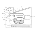
図1は、本実施形態における、非磁性一成分現像方式の現像装置の概略断面図である。
[Developer]
FIG. 1 is a schematic cross-sectional view of a non-magnetic one-component developing type developing apparatus in the present embodiment.
帯電と露光のプロセスによって感光ドラム4に形成された静電潜像をトナー像として顕像化することが、現像装置100の機能である。
The function of the developing
現像装置100には、トナー101が満たされるトナー容器部102があり、攪拌部材としての回転駆動される撹拌羽103によって現像剤供給部材としての供給ローラ104付近へトナー101を搬送しつつ撹拌する。撹拌羽103によって搬送されたトナー101を感光ドラム4上の潜像を形成するための部材としては、供給ローラ104と、現像剤規制部材としての規制ブレード105と、現像剤担持体としての現像ローラ106とがある。
The developing
[トナー]
以下に、本実施形態に適用可能なトナー101について説明する。
[toner]
Hereinafter, the
トナー101は、基本的には規制ブレード105によって擦られることで電荷を持ち、電界で動きをコントロールすることが可能となる。即ち、トナー101は規制ブレード105によって規制されることで、均一なトナー層になるとともに電荷を持ち、現像部で感光ドラム4と現像ローラ106間の電界の作用で潜像を現像することが可能となる。
The
非磁性一成分現像方式の現像装置に用いられるトナー101は、大きく分けてトナー101の母体と外添剤から構成されている。トナー101の母体は次に例示した(1)、(2)、(3)、(4)の各材料を用い、懸濁重合法、乳化重合法、粉砕法などの方法で作製する。
(1)熱可塑性樹脂(結着剤)・・・スチレンアクリル重合体、ポリスチレン、ポリエステル、ポリビニルブラチール、ポリアミド樹脂、ポリエチレン、エポキシ樹脂など。あるいは、上記の混合物。
(2)顔料(着色剤)・・・黒はカーボンブラックなど、イエローならベンジン誘導体など、マゼンタならローダミンBレーキなど、シアンなら銅フタロシアニン、スルホンアミド誘導体など。
(3)荷電制御剤・・・ネガ性トナーの場合は、電子受容性の有機錯体、塩素化パラフィン、塩素化ポリエステル、塩基過剰のポリエステル、塩素化銅フタロシアニンなど。また、ポジ性トナーの場合は、ニグロシン系の電子供与性染料、アルコキシル化アミン、アルキルアミド、キレート、顔料、4級アンモニウム塩など。
(4)充填剤・・・炭酸カルシウム、クレー、タルク、顔料など。
The
(1) Thermoplastic resin (binder): styrene acrylic polymer, polystyrene, polyester, polyvinyl bratil, polyamide resin, polyethylene, epoxy resin, and the like. Alternatively, a mixture of the above.
(2) Pigment (colorant): Black is carbon black, benzine derivative for yellow, rhodamine B lake for magenta, copper phthalocyanine, sulfonamide derivative for cyan.
(3) Charge control agent: In the case of a negative toner, an electron-accepting organic complex, chlorinated paraffin, chlorinated polyester, excess base polyester, chlorinated copper phthalocyanine, and the like. In the case of a positive toner, nigrosine electron donating dyes, alkoxylated amines, alkylamides, chelates, pigments, quaternary ammonium salts, and the like.
(4) Filler: calcium carbonate, clay, talc, pigment, etc.
トナー母体に対しての外添剤の外添は、次に例示した外添剤を用い、攪拌や熱処理などで行う。
外添剤・・・シリカ(疎水性、コロイダルなど)、金属酸化物(酸化チタン、酸化亜鉛、酸化錫)、金属錯体、荷電制御剤、など。
External addition of the external additive to the toner base is performed by stirring, heat treatment or the like using the external additive exemplified below.
External additives: silica (hydrophobic, colloidal, etc.), metal oxides (titanium oxide, zinc oxide, tin oxide), metal complexes, charge control agents, etc.
また、トナー101に関する代表的な物性値としては以下のようなものを用いる。
Further, as the typical physical property values relating to the
トナー101の体積平均粒径は、例えば、ベックマン・コールター株式会社製のコールターカウンターTA−II型で測定した場合、4〜15μm程度である。
The volume average particle diameter of the
測定装置は、体積平均粒径及び個数平均粒径の出力装置とパソコンに接続されている。コールターカウンターによる測定は、まず、1%塩化ナトリウム水溶液中に、測定するトナー101を数g分散させ、界面活性剤を数滴加える。超音波洗浄器を用いると良い分散状態ができる。その後、100μmアパーチャーを用いてトナー101の粒径を測定した後、パソコンによる処理を行い、体積平均粒径と粒度分布を算出する。
The measuring device is connected to a volume average particle size and number average particle size output device and a personal computer. In the measurement using a Coulter counter, first, several g of the
トナー101の形状については、画像解析装置で測定した形状係数SF−1の値が100〜140であり、形状係数SF−2の値が100〜130であることが好ましい。また
、上記の条件を満たしつつ、(SF−2)/(SF−1)の値を1.0以下にすることで、トナー101の諸特性のみならず、画像解析装置とのマッチングが極めて良好なものになる。
Regarding the shape of the
上記係数SF−1及びSF−2は、次のようにして得られた値によって定義されるパラメータである。まず、株式会社日立製作所製FE−SEM(S−800)を用い、倍率500倍に拡大したトナー像を100個無作為抽出する。そして、その画像情報をインターフェースを介してニコレ社製画像解析装置(Luzex3)に導入して解析を行い、次式より算出して得られた値によって係数SF−1及びSF−2が定義される。
SF−1={(MXLNG)2/AREA}×(π/4)×100
SF−2={(PERI)2/AREA}×(1/4π)×100
AREA:トナー投影面積
MXLNG:絶対最大長
PERI:周長
The coefficients SF-1 and SF-2 are parameters defined by values obtained as follows. First, using a FE-SEM (S-800) manufactured by Hitachi, Ltd., 100 toner images enlarged at a magnification of 500 times are randomly extracted. Then, the image information is introduced into the image analysis apparatus (Luxex 3) manufactured by Nicole via the interface and analyzed, and the coefficients SF-1 and SF-2 are defined by values obtained by calculating from the following equations. .
SF-1 = {(MXLNG) 2 / AREA} × (π / 4) × 100
SF-2 = {(PERI) 2 / AREA} × (1 / 4π) × 100
AREA: toner projected area MXLNG: absolute maximum length PERI: circumference
トナー形状係数SF−1はトナー粒子の丸さの度合いを示し、値が大きいほど球形から不定形となる。SF−2はトナー粒子の凹凸度合いを示し、値が大きいほどトナー表面の凹凸が顕著になる。特に、転写性や画質面でSF−1が100〜140で、SF−2が100〜130のトナーを用いると本実施形態の効果が底上げされることもある。 The toner shape factor SF-1 indicates the degree of roundness of the toner particles, and the larger the value, the more spherical the shape becomes irregular. SF-2 indicates the degree of unevenness of the toner particles, and the larger the value, the more prominent the unevenness of the toner surface. In particular, the use of toner having SF-1 of 100 to 140 and SF-2 of 100 to 130 in terms of transferability and image quality may raise the effect of this embodiment.
また、現像剤規制部材通過後のトナー層は、単位面積あたりの質量をM/S[mg/cm2]とすると、M/Sは0.2〜0.8[mg/cm2]程度が好ましい。尚、本実施形態では、負極性トナーを前提として考える。 Further, when the mass per unit area of the toner layer after passing through the developer regulating member is M / S [mg / cm 2 ], the M / S is about 0.2 to 0.8 [mg / cm 2 ]. preferable. In this embodiment, the negative toner is assumed.
[規制ブレード]
以下に、本実施形態に適用可能な規制ブレード105について説明する。
[Regulating blade]
Below, the
規制ブレード105の機能は、現像ローラ106上(現像剤担持体上)のトナー101(の層厚(量))を規制するとともにトナー101を摩擦帯電することで、均一なトナーコーティング層と現像に必要な電荷をトナー101に付与することである。
The function of the
規制ブレード105は、規制ブレード支持板金110に取り付けられている。規制ブレード支持板金110の材質としては、厚さ1mm程度のステンレス鋼などが好ましい。特に、電圧を印加する場合には、導電性の規制ブレード支持板金110を用いることにより、電源から規制ブレード105への導電経路を簡単につくることができる。規制ブレード105の材質としては、ステンレス鋼、リン青銅、樹脂、ゴムといった弾性部材が好ましい。
The
本実施形態では、規制ブレード105には、規制バイアス印加手段としての電源Vbによってバイアスが印加されるため、導電性材料を用いている。本実施形態における規制ブレード105では、金属材料を使用することで、温湿度が変化しても安定な導電性を確保できる。
In the present embodiment, a conductive material is used for the
[供給ローラ]
以下に、本実施形態に適用可能な供給ローラ104について説明する。
[Supply roller]
Below, the
供給ローラ104の機能は、現像ローラ106表面にトナー101を搬送して供給するとともに、現像ローラ106表面の現像されずに戻ってきたトナー101を剥ぎ取ることである。供給ローラ104は現像ローラ106に0〜3mm程度の侵入量で当接され、図1中の矢印で示したように、現像ローラ106に対してカウンター方向に回転駆動される
のが好ましい。
The function of the
供給ローラ104は、芯金と、芯金の周りに設けられたスポンジ層からなる。芯金の材質は、金属(ステンレス鋼、鉄、アルミ、真鋳など)、プラスチック、セラミックスなど、回転駆動時のある程度の負荷に耐えうる材質が好ましい。
The
スポンジ層は、ウレタン、シリコンなどを発泡させたものなどが好ましく、表面の発泡セル径は50〜1000μm程度が好ましい。必要に応じて、導電剤やカーボンを混ぜることで導電性を持たせ、バイアスを印加してもよい。また、スポンジ層は、単層だけではなく、2層、3層のものでも良い。 The sponge layer is preferably made of foamed urethane, silicon or the like, and the surface foam cell diameter is preferably about 50 to 1000 μm. If necessary, a conductive agent or carbon may be mixed to provide conductivity and a bias may be applied. Further, the sponge layer may be not only a single layer but also two or three layers.
供給ローラ104の物性として、硬度は、現像ローラ106への侵入量や外径差などを考慮して適正な硬度にする。また、抵抗値は、バイアスを印加する際には、必要に応じた抵抗値に調整する必要がある。
As the physical properties of the
[現像ローラ]
以下に、本実施形態の現像ローラ106について説明する。
[Development roller]
Hereinafter, the developing
供給ローラ104によって現像ローラ106上に供給されたトナー101は、現像ローラ106の回転によって、現像ローラと規制ブレードとの当接部である規制部に進入し、規制ブレード105で1〜3層程度の均一なトナー層になるように規制される。トナー規制時には、トナー101が規制ブレード105と現像ローラ106との摺擦を受けるため、電荷を持つことができる。
The
規制ブレード105によって形成された現像ローラ106上の均一なトナー層は、現像部において感光ドラム4上の静電潜像を現像する。接触現像方式においては、現像ローラ106は感光ドラム4に対して1.1〜1.6倍程度の周速比をもって回転している。さらに、現像ローラ106には、感光ドラム4上の露光部と非露光部が持つ、各電位の間の値を持つ電位を、電源Vaから印加することで、現像ローラ上において電荷をもっているトナー101を感光ドラム4上に移行させ、潜像を現像することができる。ここで、電源Vaは、現像バイアス印加手段に相当する。
The uniform toner layer on the developing
現像ローラ106は、ステンレス等の金属からなる芯金のまわりに、適度な導電性を持たせた1層以上のゴム状弾性体で構成された基層、及び、SiOx膜により形成される表層により構成されている。ゴム状弾性体(ゴム材料)は、シリコンゴム、ウレタンゴム、アクリルゴム、天然ゴム、EPDM(エチレンプロピレンジエンゴム)など一般的に用いられるゴムである。基層の抵抗値は、カーボンやカーボン樹脂粒子、金属粒子、イオン導電剤などを分散させることで得ることができる。
The developing
現像ローラ106の抵抗値は2×10⁴〜5×10⁸Ω・cmが好ましい。この範囲以下になると弾性層に流れる電流が多くなり、必要な電気容量が大きくなってしまう。また、この範囲以上になると現像時に流れる電流を阻害されやすくなる。
The resistance value of the developing
本実施形態における表面粗さは、現像ローラ106の表面粗さの指標である算術平均粗さRaを用いた。そして、算術平均粗さRaの測定は、JIS B0601に基づいて株式会社小坂研究所製の表面粗さ試験機SE−30を使用した。測定点は、現像ローラ106の回転軸方向(以下、長手方向)の左右端部に近い部分と中央部の3点を周方向に3点測定し、その合計9点の平均値を本実施形態における表面粗さとした。
As the surface roughness in this embodiment, an arithmetic average roughness Ra that is an index of the surface roughness of the developing
本実施形態における現像ローラ106の硬度測定は、日本ゴム協会標準規格SRIS0
101に準拠したアスカーC型スプリング式ゴム硬度計(高分子計器株式会社製)を用いて測定した。常温常湿(23℃、55%RH)の環境中に12時間以上放置した現像ローラ106に対して、上記硬度計を10Nの力で当接させてから30秒後の測定値とする。硬度は、現像ローラ106に対して規制ブレード105が押圧されることで形成されるニップ部が長手方向に渡って安定的に存在するためには、40〜75°が好ましい。また、接触現像方式の場合は、感光ドラムとの当接具合に応じて硬度を調節する必要がある。
The hardness of the developing
This was measured using an Asker C-type spring rubber hardness meter (manufactured by Kobunshi Keiki Co., Ltd.) in accordance with 101. The measured value is taken as 30 seconds after the hardness meter is brought into contact with the developing
後述する実施例及び比較例では、現像ローラ106の表層として、炭素原子を含む酸化ケイ素を主成分とした(SiOx)薄膜層及びウレタン樹脂層を用いている。SiOx層は、化学的気相成長(CVD)法、物理的気相成長(PVD)法、真空蒸着などの乾式法や、ディップコート、スプレーコート、ロールコートなどの湿式法で現像ローラ106の基層上に形成される。また、PVD法の具体例としては、スパッタリング、イオンプレーティングなどが挙げられる。更に、CVD法の具体例としては、プラズマCVD、熱CVD、レーザCVDなどが挙げられる。
In Examples and Comparative Examples described later, as the surface layer of the developing
本実施形態におけるSiOx膜は、プラズマCVD法による製膜を以下の方法で行った。 The SiOx film in the present embodiment was formed by the following method by plasma CVD.
芯金に基層としてのEPDMゴムを被覆した基層のみのローラを真空チャンバ内に置き、これに平行に平板電極を近接設置する。その後、チャンバ内にSiOx膜の原料ガスとなる、ガス状化した有機ケイ素化化合物、及び、必要に応じて、不活性ガス、酸化性ガス等を充満させる。そして、前記基層のみのローラを回転させながら平板電極間に、高周波電力を供給してプラズマを発生させ、原料ガスの分子が基層表面で成長し、表層膜を形成する。尚、このようにして形成するSiOx膜は、原料ガスの組成、原料ガスのチャンバ内での圧力濃度、プラズマ照射時間等のパラメータで厚さや組成を変えることが可能である。 A roller having only a base layer, in which a core metal is coated with EPDM rubber as a base layer, is placed in a vacuum chamber, and a plate electrode is placed in close proximity to the roller. Thereafter, the chamber is filled with a gasified organosilicic compound serving as a source gas for the SiOx film and, if necessary, an inert gas, an oxidizing gas, or the like. Then, high-frequency power is supplied between the flat plate electrodes while rotating the roller having only the base layer to generate plasma, and source gas molecules grow on the surface of the base layer to form a surface layer film. It should be noted that the thickness and composition of the SiOx film formed in this way can be changed by parameters such as the composition of the source gas, the pressure concentration in the chamber of the source gas, and the plasma irradiation time.
SiOとSiCの組成比が異なると物性は変化するが、その特徴的な特性として、硬度の変化が挙げられる。具体的には、組成比が、SiOのみ、もしくは、SiCのみに偏ると、SiOx膜は硬く、柔軟性が失われる傾向を示し、ひび割れ等の問題が発生しやすくなる。本実施形態においては、組成比、及び、膜厚が、後述の範囲内において、上記のひび割れ等の問題が発生しないことを確認している。 If the composition ratio of SiO and SiC is different, the physical properties change, but a characteristic change is a change in hardness. Specifically, when the composition ratio is biased toward SiO alone or SiC alone, the SiOx film tends to be hard and loses flexibility, and problems such as cracking are likely to occur. In the present embodiment, it has been confirmed that the above-described problems such as cracking do not occur within the ranges described below for the composition ratio and the film thickness.
組成比の測定には、X線光電子分光装置「Quantum2000」(アルバック・ファイ株式会社製)を用いた。そして、X線源をAlKαとして、現像ローラ表面のSiの2p軌道、O及びCの1s軌道の結合エネルギーを測定し、それぞれのピーク値から各原子の存在比を算出することで、(O/Si)及び(C/Si)の組成比を求めた。 For measurement of the composition ratio, an X-ray photoelectron spectrometer “Quantum 2000” (manufactured by ULVAC-PHI Co., Ltd.) was used. Then, by using AlKα as the X-ray source, the binding energy of the Si 2p orbit and O and C 1s orbits on the surface of the developing roller are measured, and the abundance ratio of each atom is calculated from each peak value (O / The composition ratio of Si) and (C / Si) was determined.
また、形成されたSiOx膜の膜厚は、薄膜測定装置「F20−EXR」(商品名、FILMETRICS社製)を用いて、現像ローラ106の長手方向を端部より等間隔に3箇所、かつ周方向に等間隔に3箇所の合計9箇所を測定し、得られた値の平均値である。
Further, the thickness of the formed SiOx film was measured at three locations at equal intervals from the end in the longitudinal direction of the developing
(本実施形態の作用)
以下に、本実施形態の作用について、図3を用いて説明する。
(Operation of this embodiment)
Below, the effect | action of this embodiment is demonstrated using FIG.
本実施形態では、ゴム材料の基層からなる弾性ローラの表面に、材料として硬度が高いことを特徴とするSiOx皮膜を形成した現像ローラ106を有し、規制ブレード105に印加するバイアスを変動させることを特徴とする。
In this embodiment, the developing
これによって、規制ブレード105への微粉や外添剤の融着が発生しやすい、表面粗さ
が小さい現像ローラを用いた現像装置であっても、トナー101負荷軽減効果を維持しつつ、前記問題の発生を抑制することができる。以下においては、規制ブレード105への微粉や外添剤の融着をブレード融着と呼称する。
As a result, even with a developing device using a developing roller having a small surface roughness that is likely to cause fusion of fine powder and external additives to the
図3は、現像ローラ106と規制ブレード105が形成するニップ部(規制ブレードニップ)の拡大概略図であって、ニップ部における変動バイアスがトナーに作用している様子を示す概略断面図である。図3(a)が通常の規制ブレード105によるトナーコーティングであるのに対し、図3(b)では瞬間的に規制ブレードバイアスを変動させたためにトナー101がニップ部入り口で詰まり、現像ローラ表面と規制ブレード表面が直接擦れている様子を表している。尚、図3(a),(b)に示す矢印は、現像ローラ106の回転方向を表している。
FIG. 3 is an enlarged schematic view of a nip portion (regulation blade nip) formed by the developing
図3(b)に示すような状態をつくるには、規制ブレード105の電位を現像ローラ106の電位よりトナー101の極性側に高い電位にしておき(図3(a)の状態)、そこから規制ブレード105の電位を現像ローラ106の電位に変動させれば良い。
In order to create the state shown in FIG. 3B, the potential of the
規制ブレード105の電位が高い状態では、トナー101が現像ローラ106に押し付けられるようにニップ部を通過するため、トナー101の規制ブレード通過量が多い。その状態から、規制ブレード105の電位を急激に下げると、トナー101が現像ローラ106に押し付けられる力が弱くなるため流入可能な量が制限され、この電位を維持すればニップ部入り口で流れが滞り、トナーコーティングの空白ができる。
When the potential of the
ブレード融着の発生メカニズムは、現像ローラ表面と関係が深い。 The generation mechanism of blade fusion is closely related to the surface of the developing roller.
表面粗さが粗い場合には、ニップ部において、現像ローラ基層から見て粗しの高い部分がトナー101を介することなく規制ブレード105と直接擦れる確率が高い。このため、規制ブレード105への付着物があったとしても、局所的に強い圧力で剥ぎ取ることができる。
When the surface roughness is rough, there is a high probability that a portion having a high roughness when viewed from the developing roller base layer directly rubs against the
しかし、粗しの高い部分にあるトナー101は、現像ローラ106の搬送力を局所的に受けやすく、トナー劣化の原因となっている。
However, the
そこで、表面の粗しを抑制し、鏡面にするとトナー101へのストレスが軽減されることがわかってきている。ただ、表面の粗しを抑制し、鏡面にした場合には、トナー劣化は抑制できるものの、先に述べたように、付着物を剥ぎ取ることができ難くなる。そのため、始めは付着していただけのものが、トナー規制による熱や摺擦により強固に付着して融着物となる。
Thus, it has been found that the stress on the
SiOx膜は、トナー101の離型性が高く、ゴムや樹脂の表面よりもガラス質に近いため硬い材質である。このため、図3(b)のようにトナー101を介さずに規制ブレード105と直接擦れると、わずかな粗さでも非常に高い研磨性を発揮し、規制ブレード表面に付着した微粉や外添剤をかき落とすと考えられる。
The SiOx film is a hard material because the
一方、例えばウレタンなどの樹脂膜を表層に形成した現像ローラ106を用いた場合は、膜のミクロな視点で見たときの硬度がSiOx膜よりも小さいため、規制ブレード105の付着物に対して十分な剥ぎ取り効果を発揮できないことが懸念される。
On the other hand, for example, when the developing
また、SiOx膜と異なり、表面が樹脂やゴムの材料表面の場合はタック性があるために、トナー101を強く規制する変動バイアスを印加したときでもトナー101が現像ローラ表面に残りやすい。
Further, unlike the SiOx film, when the surface is a resin or rubber material surface, there is tackiness, so that the
ウレタン樹脂膜を表層として形成した現像ローラを用いて、以下の実験例と同様の現像構成で、同様の検討を行ったところ、少なくとも表面粗さRaが0.2μm以下では、ブレード融着は発生していた。すなわち、従来からのウレタン等の樹脂膜では、ブレード融着の発生を抑えることは難しい。 Using a developing roller formed with a urethane resin film as the surface layer, the same examination was performed with the same development configuration as in the following experimental example. At least when the surface roughness Ra was 0.2 μm or less, blade fusion occurred. Was. That is, it is difficult to suppress the occurrence of blade fusion with a conventional resin film such as urethane.
<<実験例>>
以下に、後述の実施例と比較例との差異を検証するための実験例について説明する。
<< Experimental example >>
Hereinafter, experimental examples for verifying differences between examples and comparative examples described later will be described.
実験に使用した現像ローラは、A〜Eの5本で、それぞれが異なる粗さの表層を持つ。 There are five developing rollers A to E used in the experiment, each having a surface layer with a different roughness.
表1に現像ローラA〜Eの表面粗さを示す。なお、これらの5本は、すべて外形をφ12mmに揃え、基層はすべてEPDMゴム材料を用いた。表面粗さは、EPDM基層を狙いの外径であるφ12mmより大きく成型した後、研磨機の研磨条件を変えてRa0.02〜0.3μmの範囲のものを作成した。 Table 1 shows the surface roughness of the developing rollers A to E. All of these five were made to have an outer shape of φ12 mm, and the base layer was made of EPDM rubber material. The surface roughness was made larger than φ12 mm, which is the target outer diameter of the EPDM base layer, and then the polishing conditions of the polishing machine were changed to create a surface roughness within the range of Ra 0.02 to 0.3 μm.

各現像ローラ表層の物性の確認には、マルテンス硬度と膜厚を用いた。本実施形態のポイントの一つは、前述したアスカーC型硬度測定における基層も含めたローラ全体の硬度をそのままに、表層に硬質で薄膜な材料を使うことである。ナノからミクロンオーダーの薄膜の硬度(特に、本実施形態のように材質自体の硬度)を測定することは一般的に困難だが、マルテンス硬度と厚さで概ね把握できると考えられる。 Martens hardness and film thickness were used to confirm the physical properties of the surface layer of each developing roller. One of the points of this embodiment is to use a hard and thin material for the surface layer while maintaining the hardness of the entire roller including the base layer in the above-described Asker C-type hardness measurement. Although it is generally difficult to measure the hardness of a thin film of nano to micron order (particularly, the hardness of the material itself as in this embodiment), it is considered that it can be roughly grasped by the Martens hardness and thickness.
マルテンス硬度とは、ISO14577に基づいた値であり、圧子に荷重をかけながら測定対象物に押し込むことにより求められる物性値であり、
(試験荷重)/(試験荷重下での圧子の表面積)[N/mm2]
として求められる。
Martens hardness is a value based on ISO14577, and is a physical property value obtained by pushing into an object to be measured while applying a load to an indenter,
(Test load) / (Surface area of indenter under test load) [N / mm 2 ]
As required.
マルテンス硬度の測定は、超微小硬さ試験システム ピコデンターHM500(商品名、株式会社フィッシャー・インストルメンツ製)を用いて行うことが可能である。この測定装置では、四角錘の圧子、又は三角錘の圧子を、所定の比較的小さい試験荷重をかけながら測定対象物に押し込み、所定の押し込み深さに達した時点でその押し込み深さから圧子が接触している表面積を求め、上記式よりマルテンス硬度を求めるものである。つまり、定荷重測定条件で圧子を測定対象物に押し込んだ際に、押し込まれた深さに対するそのときの応力をマルテンス硬度として定義するものである。 The Martens hardness can be measured using an ultra micro hardness test system Picodenter HM500 (trade name, manufactured by Fisher Instruments Co., Ltd.). In this measuring device, a square pyramid indenter or a triangular pyramid indenter is pushed into a measurement object while applying a predetermined relatively small test load, and when the predetermined indentation depth is reached, the indenter is removed from the indentation depth. The surface area in contact is obtained, and the Martens hardness is obtained from the above formula. That is, when the indenter is pushed into the measurement object under the constant load measurement condition, the stress at that time with respect to the pushed-in depth is defined as Martens hardness.
本実施形態においては、現像ローラ表面に対し、表面から垂直方向へ、一定荷重印加速度(1mN/mm2/sec)で四角錘形状圧子を深さ0.8μmまで押し込み、測定した。測定点は、現像ローラ106の長手方向を4等分した位置である3箇所にて測定し、その相加平均した値を、現像ローラ表面のマルテンス硬度とした。
In the present embodiment, the measurement was performed by pressing the square pyramid-shaped indenter to a depth of 0.8 μm from the surface of the developing roller in a direction perpendicular to the surface at a constant load application speed (1 mN / mm 2 / sec). The measurement points were measured at three points, which are positions obtained by dividing the longitudinal direction of the developing
現像ローラ表層のSiOx膜厚は、現像ローラA〜Eにおいては、膜厚は約1.75μmに揃えた。 The SiOx film thickness of the developing roller surface layer was set to about 1.75 μm in the developing rollers A to E.
これは、少なくとも、組成比(O/Si)が1.00以上、1.95以下で、且つ、組成比(C/Si)が0.05以上、1.00以下のSiOx膜では、5μmより厚くなると、次のような問題が確認できたためである。すなわち、現像装置にセッティングした時点でゴム弾性体の柔軟な変形に追従できずにひび割れやはがれが生じてしまうことが確認できたためである。また、一方、0.05μm以下だと、均一なコートが難しくなるため、基層からのオイル成分の染み出しなどの問題も発生しやすくなるためである。ここで、SiOx膜においては、組成比(O/Si)が1.00以上、1.95以下で、且つ、組成比(C/Si)が0.05以上、1.00以下であり、膜厚が、0.05μm以上5μm以下であることが好ましい。 This is because the SiOx film having a composition ratio (O / Si) of 1.00 or more and 1.95 or less and a composition ratio (C / Si) of 0.05 or more and 1.00 or less is less than 5 μm. This is because the following problems were confirmed when the thickness was increased. That is, it was confirmed that cracking and peeling occurred without being able to follow the flexible deformation of the rubber elastic body when it was set in the developing device. On the other hand, if the thickness is 0.05 μm or less, uniform coating becomes difficult, and problems such as oil component seepage from the base layer are likely to occur. Here, in the SiOx film, the composition ratio (O / Si) is 1.00 or more and 1.95 or less, and the composition ratio (C / Si) is 0.05 or more and 1.00 or less. The thickness is preferably 0.05 μm or more and 5 μm or less.
ここで、上述した薄膜を形成する前の現像ローラ表面のマルテンス硬度をH1とし、表層としてのSiOx膜を基層上に成膜した状態におけるマルテンス硬度をH2とする。この場合、本実験例で使用した現像ローラA〜Eの表面硬度は、H1が約2.9[N/mm]で、H2が約1.2[N/mm]であった。SiOx膜は非常に薄膜にもかかわらず、マルテンス硬度に明確な差が出ていた。 Here, the Martens hardness on the surface of the developing roller before forming the thin film described above is H1, and the Martens hardness in a state where the SiOx film as the surface layer is formed on the base layer is H2. In this case, the surface hardness of the developing rollers A to E used in this experimental example was about 2.9 [N / mm] for H1 and about 1.2 [N / mm] for H2. Although the SiOx film was very thin, a clear difference was found in the Martens hardness.
一方、現像ローラ全体の硬度を示すアスカーC型硬度計による硬度は、現像ローラA〜Eで、SiOx膜成膜前後にかかわらず、すべて63°であった。 On the other hand, the hardness by the Asker C-type hardness meter indicating the hardness of the entire developing roller was 63 ° with the developing rollers A to E, regardless of whether the SiOx film was formed or not.
表2は、現像ローラ106及び規制ブレード105に印加するACバイアスの電位と周波数を示している。
Table 2 shows the AC bias potential and frequency applied to the developing
規制ブレード105の変動バイアスは必ずしも波形が矩形のバイアスである必要はないが、実施が容易なため、本実施形態では、Duty50%の矩形ACバイアスを変動バイアスとして用いた。そのため、周波数fの値の逆数の半分が、本実施形態における規制ブレード105に印加する最小の電圧Vb_Lの印加時間Tlということになる。
Although the fluctuation bias of the
本実験例においては、周波数は1200Hzに固定した。表2中では現像ローラの電位をバイアスVdevとした。また、規制ブレード105に印加される電圧のうちトナー101の帯電極性側の最大の電圧、最小の電圧をそれぞれVb_H、Vb_Lとし、変動の振幅に相当する電位差を、|Vb_H−Vb_L|とした。また、現像ローラ106と規制ブレード105の間にかかる電位差は、|Vb_H−Vdev|とした。
In this experimental example, the frequency was fixed at 1200 Hz. In Table 2, the potential of the developing roller is the bias Vdev. In addition, among the voltages applied to the
図4は、本実施形態において、各バイアスの相対的な電位関係を示す図である。図5は、従来技術における各バイアスの相対的な電位関係を示す図である。 FIG. 4 is a diagram showing the relative potential relationship of each bias in the present embodiment. FIG. 5 is a diagram showing a relative potential relationship of each bias in the prior art.
バイアスA〜Dまでは、図4に示したような電位関係になる。バイアスEは、振幅が0であるためDCバイアスのみが印加されていることになる。バイアスFは、規制ブレード
電位が現像ローラ電位よりも下、即ち、トナー101の極性と逆極性側に大きい設定となっており、図5に示したような電位関係になっている。
The biases A to D have a potential relationship as shown in FIG. Since the bias E has an amplitude of 0, only the DC bias is applied. The bias F is set such that the regulating blade potential is lower than the developing roller potential, that is, on the side opposite to the polarity of the
表1に示した各現像ローラと表2に示した各バイアスを組み合わせて、通常環境(温度24℃/湿度50%)における耐久実験を行った。 A durability experiment in a normal environment (temperature 24 ° C./humidity 50%) was performed by combining each developing roller shown in Table 1 and each bias shown in Table 2.
規制ブレード105への変動バイアス印加は、現像ローラが回転しているときは常に印加した。耐久実験には、図2に示したような画像形成装置としてのプリンタを用いた。
The variable bias was applied to the
現像ローラ(表面)の回転速度vは、120mm/secであった。トナー充填量は、100gであった。印字率1%の画像パターンで、2枚間欠プリントの通紙耐久テストを行い、11000枚まで通紙したところで画像の評価を行った。 The rotation speed v of the developing roller (surface) was 120 mm / sec. The toner filling amount was 100 g. A two-sheet intermittent printing paper endurance test was performed with an image pattern having a printing rate of 1%, and the image was evaluated when up to 11,000 sheets were passed.
ブレード融着は、ベタ画像におけるスジムラで発生の有無を判断した。また、ガサツキ画像の評価はベタ画像から薄いハーフトーンまでを目視で判断した。尚、ガサツキ画像とは、トナー101の外添剤がはがれたり遊離したりといった、所謂トナー劣化に起因する画像の乱れである。
The presence or absence of occurrence of blade fusion due to unevenness in the solid image was determined. In addition, the evaluation of the rough image was visually judged from a solid image to a thin halftone. Note that the rough image is a disturbance in the image caused by so-called toner deterioration such that the external additive of the
表3に実験条件の組合せ、及び、その結果として発生した問題の概要を示した。表3においては、現像ローラA〜EとバイアスA〜Fの組合せを表している。各組み合わせにおいて発生した最も大きな問題がその位置に記載されている。 Table 3 summarizes the combinations of experimental conditions and the resulting problems. In Table 3, combinations of developing rollers A to E and biases A to F are shown. The biggest problem that occurred in each combination is listed at that location.
バイアスAを用いたものは、現像ローラの構成にかかわらず、放電跡が発生している。 In the case of using the bias A, discharge traces are generated regardless of the configuration of the developing roller.
これは、表2における最大電位差|Vb_H−Vdev|が500Vを超えたためと考えられる。パッシェンの放電開始電圧から推測すると、600V前後が放電閾値となるが、ニップ部にはトナー101が介在していることもあり、局所的には放電が開始されていると考えられる。そのため、画像には斑点のような意図しないパターンが発生してしまった。すなわち、
|Vb_H−Vdev|≦500V
の関係を満たすことで、放電跡の発生を防止することができる。
This is thought to be because the maximum potential difference | Vb_H− Vdev | in Table 2 exceeded 500V. Assuming from Paschen's discharge start voltage, the discharge threshold is around 600 V, but the
| Vb_H- Vdev | ≦ 500V
By satisfying this relationship, the occurrence of discharge traces can be prevented.
バイアスBを用いたものは、現像ローラA〜Cでは大きな問題は発生しなかった。現像ローラDでは、ACバイアスを印加しているにもかかわらずブレード融着が発生した。 In the case of using the bias B, no major problem occurred in the developing rollers A to C. In the developing roller D, blade fusion occurred despite the AC bias being applied.
これは、バイアスによらず、現像ローラ表面粗さが鏡面に近く、規制ブレード表面と擦れたものの、付着物を剥ぎ取るほどの作用を発揮できなかったためと考えられる。また、現像ローラEを用いたものは、バイアスA〜Fによらず、ローラ表面の粗しに起因するガサツキ画像が発生した。 This is presumably because the surface roughness of the developing roller was close to a mirror surface and rubbed against the surface of the regulating blade regardless of the bias, but the effect of peeling off the deposits could not be exhibited. Further, in the case of using the developing roller E, a rough image due to the rough surface of the roller was generated regardless of the biases A to F.
バイアスC,Dを用いたものは、バイアスBと同様に、現像ローラA〜Cにおいて良好
な画像が得られた。
In the case of using the biases C and D, like the bias B, good images were obtained on the developing rollers A to C.
したがって、現像ローラの表面粗さRa[μm]を、
0.05≦Ra≦0.2
と設定することで、大きな問題の発生を防止することができる。
Therefore, the surface roughness Ra [μm] of the developing roller is
0.05 ≦ Ra ≦ 0.2
The occurrence of a major problem can be prevented by setting.
バイアスEを用いたものは、現像ローラA〜Dではブレード融着が発生していた。 In the case of using the bias E, blade fusion occurred in the developing rollers A to D.
これは、バイアスEがDCバイアスであるため、表面粗さが極端に小さい現像ローラ表面と規制ブレード105が擦れることなく耐久が進み、付着物が規制ブレード表面に融着したものと考えられる。現像ローラEの場合は、表面粗さが比較的大きいため、粗しの山が高い部分で規制ブレード105と直接擦れるため、DCバイアスでもブレード融着が発生しなかった。しかし、粗しの作用によりトナー101への負荷は増大し、特にハーフトーン画像においてガサツキが見られた。
This is presumably because the bias E is a DC bias, and the development roller surface with extremely small surface roughness and the
したがって、規制ブレード105に印加するバイアスをACバイアス(AC電圧)とすることで、ブレード融着の発生や、ガサツキの発生を防止することができる。
Therefore, by making the bias applied to the
バイアスFを用いたものは、現像ローラ構成にかかわらず、ガサツキ画像が発生した。 The image using the bias F generated a rough image regardless of the configuration of the developing roller.
これは、次のように考えられる。バイアスFを用いたものは、表2において、ACバイアスの振幅に相当する|Vb_H−Vb_L|の値が、最大電位差|Vb_H−Vdev|よりも大きい状態、即ち、図5に示したような電位関係になる。このため、トナー101の受ける電界の力が逆転することに起因して、従来見られるような攪拌・振動作用の大きいACバイアスとなり、トナー101の母体と外添剤がトナー101から遊離しやすくなったためと考えられる。
This is considered as follows. The bias F is used in Table 2, in which the value of | Vb_H−Vb_L | corresponding to the amplitude of the AC bias is larger than the maximum potential difference | Vb_H− Vdev |, that is, the potential as shown in FIG. Become a relationship. For this reason, the force of the electric field received by the
したがって、図4に示した電位関係、すなわち、
|Vb_H−Vb_L|≦|Vb_H−Vdev|
|Vdev−Vb_L|≦|Vdev−Vb_H|
の関係を満たすことで、ガサツキの発生を防止することができる。
Therefore, the potential relationship shown in FIG.
| Vb_H−Vb_L | ≦ | Vb_H− Vdev |
| Vdev−Vb_L | ≦ | Vdev−Vb_H |
Satisfaction can be prevented by satisfying this relationship.
また、表2から、
100V≦|Vb_H−Vb_L|
の関係が成立していることがわかる。
From Table 2 ,
100V ≦ | Vb_H−Vb_L |
It can be seen that the relationship is established.
以上の実験結果により、現像ローラD,Eは、全てのバイアス条件で問題が発生し、また、バイアスA,E,Fは、全ての現像ローラで問題が発生し、バイアスB〜Dにおいては、現像ローラの表面粗さの設定によって、問題が発生しなかったことが分かる。 From the above experimental results, the developing rollers D and E have problems under all bias conditions, and the biases A, E, and F have problems with all developing rollers. It can be seen that no problem occurred depending on the setting of the surface roughness of the developing roller.
すなわち、これら実験結果から、
0.05≦Ra≦0.2
100V≦|Vb_H−Vb_L|≦|Vb_H−Vdev|≦500V
|Vdev−Vb_L|≦|Vdev−Vb_H|
の関係を満たす場合に、問題の発生を防止できることがわかる。
That is, from these experimental results,
0.05 ≦ Ra ≦ 0.2
100V ≦ | Vb_H−Vb_L | ≦ | Vb_H− Vdev | ≦ 500V
| Vdev−Vb_L | ≦≦ Vdev−Vb_H |
It can be seen that the occurrence of the problem can be prevented when the above relationship is satisfied.
以上の実験例を踏まえて、実施例及び比較例を以下に示す。 Based on the above experimental examples, examples and comparative examples are shown below.
<実施例及び比較例>
表4は、実施例及び比較例の現像ローラ構成、規制ブレード105のバイアス、周波数
などを表したものである。実施例及び比較例においても、実験例と同様の画像評価を行い、その結果概要を画像評価の欄に表している。規制ブレード105に印加しているバイアスも実験例と同様に、DUTY50%のACバイアスである。規制ブレードバイアスの最小電位Vb_Lの印加時間を周波数より換算したものも表中に示してある。
<Examples and Comparative Examples>
Table 4 shows the developing roller configuration, the bias of the
実施例1は、実験例で示した現像ローラAとバイアスBを組合せ、さらに、規制ブレードバイアスの周波数を変えたものである。画像評価は、問題なく良好な画像となった。 In Example 1, the developing roller A and the bias B shown in the experimental example are combined, and the frequency of the regulating blade bias is changed. The image evaluation was a good image without problems.
実施例2は、実験例で示した現像ローラBとバイアスCを組合せ、さらに、規制ブレードバイアスの周波数を変えたものである。画像評価は、問題なく良好な画像となった。 In Example 2, the developing roller B and the bias C shown in the experimental example are combined, and the frequency of the regulating blade bias is changed. The image evaluation was a good image without problems.
実施例3は、実験例で示した現像ローラCとバイアスDを組合せ、さらに、規制ブレードバイアスの周波数を変えたものである。画像評価は、問題なく良好な画像となった。 In Example 3, the developing roller C and the bias D shown in the experimental example are combined, and the frequency of the regulating blade bias is changed. The image evaluation was a good image without problems.
実施例4,5は、実施例1においてVb_L印加時間Tlを変更したものである。 In the fourth and fifth embodiments, the Vb_L application time Tl is changed in the first embodiment.
実施例4においては、時間Tlが長く、目視では存在を確認するのが困難な程度のラインが画像上で観察された。 In Example 4, the time Tl was long, and a line that was difficult to confirm by visual observation was observed on the image.
実施例5においては、時間Tlが短く、ブレード融着はなかったものの、ブレードへの微粉の付着が若干確認された。問題ない程度のスジムラが画像上で観察された。 In Example 5, although the time Tl was short and there was no blade fusion, a slight amount of fine powder adhered to the blade was confirmed. A non-problematic level of unevenness was observed on the image.
比較例1は、実験例で示した現像ローラAとバイアスBを組合せ、さらに、規制ブレードバイアスの周波数を変えたものである。画像評価において、ブレード融着に起因したと思われるスジムラが発生したので、規制ブレード表面を観察したところ、ブレード融着が確認できた。 In Comparative Example 1, the developing roller A and the bias B shown in the experimental example are combined, and the frequency of the regulating blade bias is changed. In the image evaluation, stripe unevenness, which was thought to be caused by blade fusion, occurred, and when the regulated blade surface was observed, blade fusion was confirmed.
比較例2は、実験例で示した現像ローラAとバイアスBを組合せ、さらに、規制ブレードバイアスの周波数を変えたものである。画像評価において、通紙耐久結果を待たずして、ACバイアス周期に起因する明確なラインが発生していた。 In Comparative Example 2, the developing roller A and the bias B shown in the experimental example are combined, and the frequency of the regulating blade bias is changed. In the image evaluation, a clear line due to the AC bias cycle was generated without waiting for the paper passing durability result.
表4より、現像ローラの回転速度v=120×10−3[m/sec]におけるVb_L印加時間Tlの適正範囲は、
0.00025≦Tl[sec]≦0.001
であると考えられる。これは、印加時間Tlの間に現像ローラ表面がブレードに対して進む長さに換算すると、
30×10−6≦(Tl×v(=120×10−3))[m]≦120×10−6
と表現できる。
From Table 4, the appropriate range of the Vb_L application time Tl at the rotation speed v = 120 × 10 −3 [m / sec] of the developing roller is
0.00025 ≦ Tl [sec] ≦ 0.001
It is thought that. This is converted into the length that the developing roller surface advances with respect to the blade during the application time Tl.
30 × 10 −6 ≦ (Tl × v (= 120 × 10 −3 )) [m] ≦ 120 × 10 −6
Can be expressed.
本発明の効果は、Vb_L印加時間Tlの間に現像ローラ表面とブレード表面が擦れる
ことで得られる。よって、実施例で使用したv=120×10−3[m/sec]における印加時間Tlの適正範囲そのものではなく、印加時間Tlの間に現像ローラ表面がブレードに対して進む長さ、即ち、Tlとvの積の値が適正範囲であればTlとvを変えても同様の効果が得られると考えられる。
The effect of the present invention is obtained by rubbing the developing roller surface and the blade surface during the Vb_L application time Tl. Therefore, not the proper range of the application time Tl at v = 120 × 10 −3 [m / sec] used in the example, but the length that the developing roller surface advances with respect to the blade during the application time Tl, that is, If the value of the product of Tl and v is in an appropriate range, it is considered that the same effect can be obtained even if Tl and v are changed.
つまり、本実施例から得られた値を用いて、任意のTlとvに対して、
30×10−6≦(Tl×v)[m]≦120×10−6
が満たされていれば良い。
In other words, using the values obtained from this example, for any Tl and v,
30 × 10 -6 ≦ (Tl × v) [m] ≦ 120 × 10 -6
As long as is satisfied.
上記のことから、任意の現像ローラ回転速度vを決定した場合、適正なVb_L印加時間Tlの範囲は、
30×10−6/v≦Tl[sec]≦120×10−6/v
の式によって決めることができる。
From the above, when an arbitrary developing roller rotation speed v is determined, the appropriate range of the Vb_L application time Tl is
30 × 10 −6 / v ≦ Tl [sec] ≦ 120 × 10 −6 / v
It can be determined by the following formula.
(作用に関する考察)
実施例1〜5においては、現像ローラの表面粗さ、バイアスの電位設定、バイアスの周波数が適正なため、画像評価において良好な結果となった。これは、バイアスの変動によってできた現像ローラ表面のトナーコーティングの空白領域において、硬質で適度な粗さを持ったSiOx薄膜の現像ローラ表面が規制ブレード表面と擦れたため、規制ブレード表面の付着物を押し流すことができたからと考えられる。
(Consideration on action)
In Examples 1 to 5, since the surface roughness of the developing roller, the bias potential setting, and the bias frequency were appropriate, good results were obtained in image evaluation. This is because, in the blank area of the toner coating on the surface of the developing roller due to the fluctuation of the bias, the hard and moderately rough SiOx thin film developing roller surface rubbed against the regulating blade surface. It is thought that it was able to be washed away.
一方、比較例1においては、実施例1と同じ現像ローラとバイアス設定を使用しているにもかかわらず、ブレード融着が発生してしまった。これは、現像ローラの回転速度vに対してバイアスの周波数が高すぎたため(Vb_Lが短すぎたため)、充分なトナーコーティングの空白領域が得られなかったためであると考えられる。 On the other hand, in Comparative Example 1, although the same developing roller and bias setting as in Example 1 were used, blade fusion occurred. This is presumably because a sufficient blank area of the toner coating could not be obtained because the bias frequency was too high with respect to the rotation speed v of the developing roller (Vb_L was too short).
また、比較例2については、周波数が低すぎたため、トナーコーティングの空白領域が目立ったと考えられる。 In Comparative Example 2, it is considered that the blank area of the toner coating was conspicuous because the frequency was too low.
この他、表面粗さが最も小さい現像ローラDにおいて周波数を変えてみたが、この場合も、ブレード融着は発生してしまった。これは、鏡面のような面では、充分な摩擦が得られず、規制ブレード上の付着物を押し流すことができなかったためであると考えられる。 In addition, although the frequency was changed in the developing roller D having the smallest surface roughness, blade fusion also occurred in this case. This is presumably because sufficient friction could not be obtained on a mirror-like surface and the deposit on the regulating blade could not be swept away.
以上の実験例及び実施例から、表層が表面粗さRaが0.05〜0.2で、SiOx薄膜から形成され、基層が弾性体の現像ローラを用いて、規制ブレード105の電位を、次のように設定することで、良好な画像が得られることがわかる。 From the above experimental examples and examples, the surface layer is formed of a SiOx thin film having a surface roughness Ra of 0.05 to 0.2, and the base layer is made of an elastic developing roller. It can be seen that a good image can be obtained by setting as described above.
すなわち、
100V≦|Vb_H−Vb_L|≦|Vb_H−Vdev|≦500V、
30×10−6/v≦Tl[sec]≦120×10−6/v
の関係を満足するように設定することで、良好な画像が得られることがわかる。
That is,
100V ≦ | Vb_H−Vb_L | ≦ | Vb_H− Vdev | ≦ 500V,
30 × 10 −6 / v ≦ Tl [sec] ≦ 120 × 10 −6 / v
It can be seen that a good image can be obtained by setting so as to satisfy the above relationship.
以上説明したように、本実施形態では、硬質で薄膜な表層とゴム弾性体の基層とを有する現像ローラ106を備え、規制ブレード105に変動バイアスを印加する構成としている。このような構成とすることで、規制ブレード105に付着した付着物を擦り取る作用を得ることができる。したがって、現像装置において、高画質化又は高耐久性のために粗さの小さい表面を持つ現像ローラを用いた場合であっても、所謂ブレード融着に起因するスジムラ画像などの発生を防止することができる。これにより、トナー劣化に起因するフィルミング、カブリ、濃度ムラ、ガサツキなどの問題の発生を防止することができ、良好な画像を得ることができる。
As described above, in the present embodiment, the developing
なお、本実施形態では、現像ローラ回転中は、常に変動バイアスを用いる構成を述べたが、非画像形成時もしくは画像形成時のみに同様の変動バイアスを用いることでも同様の効果が得られる。 In this embodiment, the configuration in which the variable bias is always used while the developing roller is rotating is described. However, the same effect can be obtained by using the same variable bias only during non-image formation or image formation.
また、本実施形態の現像装置及びプロセスカートリッジは、カラーの画像形成装置などにも適用可能である。 Further, the developing device and the process cartridge according to the present embodiment can be applied to a color image forming apparatus.
1 画像形成装置
100 現像装置
101 トナー
104 供給ローラ
105 規制ブレード
106 現像ローラ
DESCRIPTION OF SYMBOLS 1
Claims (3)
前記現像剤を担持する現像剤担持体と、
導電性材料により構成され、前記現像剤担持体上の前記現像剤を規制する現像剤規制部材と、
前記現像剤規制部材にバイアスを印加する規制バイアス印加手段と、
前記現像剤担持体にバイアスVdevを印加する現像バイアス印加手段と、
を有する非磁性一成分現像方式の現像装置において、
前記現像剤担持体は、ゴム状弾性体からなる基層と、SiOx薄膜からなる表層とにより構成され、
前記規制バイアス印加手段は、前記現像剤規制部材にAC電圧を印加するものであって、
前記現像剤担持体の表面粗さをRa[μm]とし、
前記規制バイアス印加手段により前記現像剤規制部材に印加される電圧のうち、前記現像剤の帯電極性側の最大の電圧をVb_H、最小の電圧をVb_Lとし、
前記現像剤担持体表面の回転速度をv[m/sec]、前記規制バイアス印加手段により前記現像剤規制部材に印加される前記最小の電圧Vb_Lの印加時間をTl[sec]とした場合に、
0.05≦Ra≦0.2、
|Vdev−Vb_L|≦|Vdev−Vb_H|、
100V≦|Vb_H−Vb_L|≦|Vb_H−Vdev|≦500V、
かつ、
30×10−6/v≦Tl≦120×10−6/v
を満たすことを特徴とする現像装置。 Developer,
A developer carrying member carrying the developer;
A developer regulating member that is made of a conductive material and regulates the developer on the developer carrying member;
Regulation bias applying means for applying a bias to the developer regulating member;
Developing bias applying means for applying a bias Vdev to the developer carrying member;
In a developing apparatus of a non-magnetic one-component development system having
The developer carrier is composed of a base layer made of a rubber-like elastic body and a surface layer made of a SiOx thin film,
The regulation bias applying means applies an AC voltage to the developer regulating member,
The surface roughness of the developer carrier is Ra [μm] ,
Of the voltages applied to the developer regulating member by the regulating bias applying means, the maximum voltage on the charging polarity side of the developer is Vb_H, and the minimum voltage is Vb_L.
When the rotation speed of the surface of the developer carrying member is v [m / sec] and the application time of the minimum voltage Vb_L applied to the developer regulating member by the regulating bias applying unit is Tl [sec],
0.05 ≦ Ra ≦ 0.2,
| Vdev−Vb_L | ≦ | Vdev−Vb_H |,
100V ≦ | Vb_H−Vb_L | ≦ | Vb_H− Vdev | ≦ 500V,
And,
30 × 10 −6 / v ≦ Tl ≦ 120 × 10 −6 / v
A developing device characterized by satisfying the above.
前記像担持体に現像作用を行う請求項1に記載の現像装置と、
を備えることを特徴とする画像形成装置。 An image carrier;
The developing device according to claim 1, which performs a developing action on the image carrier;
An image forming apparatus comprising:
Priority Applications (1)
| Application Number | Priority Date | Filing Date | Title |
|---|---|---|---|
| JP2008181697A JP5147578B2 (en) | 2008-07-11 | 2008-07-11 | Developing device, process cartridge, and image forming apparatus |
Applications Claiming Priority (1)
| Application Number | Priority Date | Filing Date | Title |
|---|---|---|---|
| JP2008181697A JP5147578B2 (en) | 2008-07-11 | 2008-07-11 | Developing device, process cartridge, and image forming apparatus |
Publications (3)
| Publication Number | Publication Date |
|---|---|
| JP2010020168A JP2010020168A (en) | 2010-01-28 |
| JP2010020168A5 JP2010020168A5 (en) | 2011-08-25 |
| JP5147578B2 true JP5147578B2 (en) | 2013-02-20 |
Family
ID=41705119
Family Applications (1)
| Application Number | Title | Priority Date | Filing Date |
|---|---|---|---|
| JP2008181697A Expired - Fee Related JP5147578B2 (en) | 2008-07-11 | 2008-07-11 | Developing device, process cartridge, and image forming apparatus |
Country Status (1)
| Country | Link |
|---|---|
| JP (1) | JP5147578B2 (en) |
Families Citing this family (2)
| Publication number | Priority date | Publication date | Assignee | Title |
|---|---|---|---|---|
| JP5517522B2 (en) * | 2008-09-12 | 2014-06-11 | キヤノン株式会社 | Developing roller, electrophotographic process cartridge, and electrophotographic image forming apparatus |
| JP5328287B2 (en) * | 2008-10-17 | 2013-10-30 | キヤノン株式会社 | Electrophotographic image forming apparatus |
-
2008
- 2008-07-11 JP JP2008181697A patent/JP5147578B2/en not_active Expired - Fee Related
Also Published As
| Publication number | Publication date |
|---|---|
| JP2010020168A (en) | 2010-01-28 |
Similar Documents
| Publication | Publication Date | Title |
|---|---|---|
| US6389254B2 (en) | Charging member holding charge accelerating particles in a continuous bubble | |
| KR100730679B1 (en) | Developing apparatus, cartridge and image forming apparatus | |
| JP3292156B2 (en) | Charging member, charging method, charging device, image forming apparatus, and process cartridge | |
| JP4920981B2 (en) | Image forming apparatus | |
| JP2001042641A (en) | Developer, developing method, developing device and component therefor, and image forming device | |
| JP2003316115A (en) | Charging member, charging device, and image forming apparatus | |
| JP5196871B2 (en) | Developing roller, developing device using the same, electrophotographic apparatus, and process cartridge | |
| JP5147578B2 (en) | Developing device, process cartridge, and image forming apparatus | |
| JP2010230772A (en) | Image forming apparatus | |
| JP2010020168A5 (en) | ||
| JP2002023480A (en) | Image forming device | |
| JP2013073003A (en) | Developing device and image forming apparatus | |
| JP3647409B2 (en) | Charging device, process cartridge, image forming apparatus, roller-shaped charging member | |
| JP4307034B2 (en) | Image forming apparatus | |
| JP2001042646A (en) | Image forming device | |
| JP5279361B2 (en) | Image forming apparatus | |
| JP3780068B2 (en) | Image forming method | |
| JP2002365828A (en) | Image forming method | |
| JP2006284728A (en) | Development apparatus and image forming method | |
| JP7183029B2 (en) | Cleaning device, cartridge and image forming device | |
| JP4208395B2 (en) | Developing apparatus, apparatus unit, and image forming apparatus | |
| JP5550490B2 (en) | Discharge device | |
| JPH037972A (en) | Developing and cleaning method | |
| JPH11119547A (en) | Developing device, process cartridge and image forming device | |
| JP2009288539A (en) | Image forming apparatus |
Legal Events
| Date | Code | Title | Description |
|---|---|---|---|
| A521 | Written amendment |
Free format text: JAPANESE INTERMEDIATE CODE: A523 Effective date: 20110707 |
|
| A621 | Written request for application examination |
Free format text: JAPANESE INTERMEDIATE CODE: A621 Effective date: 20110707 |
|
| TRDD | Decision of grant or rejection written | ||
| A977 | Report on retrieval |
Free format text: JAPANESE INTERMEDIATE CODE: A971007 Effective date: 20121024 |
|
| A01 | Written decision to grant a patent or to grant a registration (utility model) |
Free format text: JAPANESE INTERMEDIATE CODE: A01 Effective date: 20121030 |
|
| A61 | First payment of annual fees (during grant procedure) |
Free format text: JAPANESE INTERMEDIATE CODE: A61 Effective date: 20121127 |
|
| FPAY | Renewal fee payment (event date is renewal date of database) |
Free format text: PAYMENT UNTIL: 20151207 Year of fee payment: 3 |
|
| LAPS | Cancellation because of no payment of annual fees |