WO2013061735A1 - Light-emitting diode, method for manufacturing light-emitting diode, light-emitting diode lamp and illumination device - Google Patents
Light-emitting diode, method for manufacturing light-emitting diode, light-emitting diode lamp and illumination device Download PDFInfo
- Publication number
- WO2013061735A1 WO2013061735A1 PCT/JP2012/075572 JP2012075572W WO2013061735A1 WO 2013061735 A1 WO2013061735 A1 WO 2013061735A1 JP 2012075572 W JP2012075572 W JP 2012075572W WO 2013061735 A1 WO2013061735 A1 WO 2013061735A1
- Authority
- WO
- WIPO (PCT)
- Prior art keywords
- layer
- light emitting
- emitting diode
- light
- substrate
- Prior art date
Links
Images


Classifications
-
- H—ELECTRICITY
- H01—ELECTRIC ELEMENTS
- H01L—SEMICONDUCTOR DEVICES NOT COVERED BY CLASS H10
- H01L33/00—Semiconductor devices with at least one potential-jump barrier or surface barrier specially adapted for light emission; Processes or apparatus specially adapted for the manufacture or treatment thereof or of parts thereof; Details thereof
- H01L33/005—Processes
- H01L33/0062—Processes for devices with an active region comprising only III-V compounds
- H01L33/0066—Processes for devices with an active region comprising only III-V compounds with a substrate not being a III-V compound
-
- H—ELECTRICITY
- H01—ELECTRIC ELEMENTS
- H01L—SEMICONDUCTOR DEVICES NOT COVERED BY CLASS H10
- H01L33/00—Semiconductor devices with at least one potential-jump barrier or surface barrier specially adapted for light emission; Processes or apparatus specially adapted for the manufacture or treatment thereof or of parts thereof; Details thereof
- H01L33/02—Semiconductor devices with at least one potential-jump barrier or surface barrier specially adapted for light emission; Processes or apparatus specially adapted for the manufacture or treatment thereof or of parts thereof; Details thereof characterised by the semiconductor bodies
- H01L33/14—Semiconductor devices with at least one potential-jump barrier or surface barrier specially adapted for light emission; Processes or apparatus specially adapted for the manufacture or treatment thereof or of parts thereof; Details thereof characterised by the semiconductor bodies with a carrier transport control structure, e.g. highly-doped semiconductor layer or current-blocking structure
-
- H—ELECTRICITY
- H01—ELECTRIC ELEMENTS
- H01L—SEMICONDUCTOR DEVICES NOT COVERED BY CLASS H10
- H01L33/00—Semiconductor devices with at least one potential-jump barrier or surface barrier specially adapted for light emission; Processes or apparatus specially adapted for the manufacture or treatment thereof or of parts thereof; Details thereof
- H01L33/36—Semiconductor devices with at least one potential-jump barrier or surface barrier specially adapted for light emission; Processes or apparatus specially adapted for the manufacture or treatment thereof or of parts thereof; Details thereof characterised by the electrodes
- H01L33/38—Semiconductor devices with at least one potential-jump barrier or surface barrier specially adapted for light emission; Processes or apparatus specially adapted for the manufacture or treatment thereof or of parts thereof; Details thereof characterised by the electrodes with a particular shape
-
- H—ELECTRICITY
- H01—ELECTRIC ELEMENTS
- H01L—SEMICONDUCTOR DEVICES NOT COVERED BY CLASS H10
- H01L21/00—Processes or apparatus adapted for the manufacture or treatment of semiconductor or solid state devices or of parts thereof
- H01L21/02—Manufacture or treatment of semiconductor devices or of parts thereof
- H01L21/02104—Forming layers
- H01L21/02365—Forming inorganic semiconducting materials on a substrate
- H01L21/02367—Substrates
- H01L21/0237—Materials
- H01L21/02387—Group 13/15 materials
- H01L21/02395—Arsenides
-
- H—ELECTRICITY
- H01—ELECTRIC ELEMENTS
- H01L—SEMICONDUCTOR DEVICES NOT COVERED BY CLASS H10
- H01L21/00—Processes or apparatus adapted for the manufacture or treatment of semiconductor or solid state devices or of parts thereof
- H01L21/02—Manufacture or treatment of semiconductor devices or of parts thereof
- H01L21/02104—Forming layers
- H01L21/02365—Forming inorganic semiconducting materials on a substrate
- H01L21/02436—Intermediate layers between substrates and deposited layers
- H01L21/02439—Materials
- H01L21/02455—Group 13/15 materials
- H01L21/02461—Phosphides
-
- H—ELECTRICITY
- H01—ELECTRIC ELEMENTS
- H01L—SEMICONDUCTOR DEVICES NOT COVERED BY CLASS H10
- H01L21/00—Processes or apparatus adapted for the manufacture or treatment of semiconductor or solid state devices or of parts thereof
- H01L21/02—Manufacture or treatment of semiconductor devices or of parts thereof
- H01L21/02104—Forming layers
- H01L21/02365—Forming inorganic semiconducting materials on a substrate
- H01L21/02436—Intermediate layers between substrates and deposited layers
- H01L21/02439—Materials
- H01L21/02455—Group 13/15 materials
- H01L21/02463—Arsenides
-
- H—ELECTRICITY
- H01—ELECTRIC ELEMENTS
- H01L—SEMICONDUCTOR DEVICES NOT COVERED BY CLASS H10
- H01L21/00—Processes or apparatus adapted for the manufacture or treatment of semiconductor or solid state devices or of parts thereof
- H01L21/02—Manufacture or treatment of semiconductor devices or of parts thereof
- H01L21/02104—Forming layers
- H01L21/02365—Forming inorganic semiconducting materials on a substrate
- H01L21/02518—Deposited layers
- H01L21/02521—Materials
- H01L21/02538—Group 13/15 materials
- H01L21/02543—Phosphides
-
- H—ELECTRICITY
- H01—ELECTRIC ELEMENTS
- H01L—SEMICONDUCTOR DEVICES NOT COVERED BY CLASS H10
- H01L21/00—Processes or apparatus adapted for the manufacture or treatment of semiconductor or solid state devices or of parts thereof
- H01L21/02—Manufacture or treatment of semiconductor devices or of parts thereof
- H01L21/02104—Forming layers
- H01L21/02365—Forming inorganic semiconducting materials on a substrate
- H01L21/02518—Deposited layers
- H01L21/02521—Materials
- H01L21/02538—Group 13/15 materials
- H01L21/02546—Arsenides
-
- H—ELECTRICITY
- H01—ELECTRIC ELEMENTS
- H01L—SEMICONDUCTOR DEVICES NOT COVERED BY CLASS H10
- H01L21/00—Processes or apparatus adapted for the manufacture or treatment of semiconductor or solid state devices or of parts thereof
- H01L21/02—Manufacture or treatment of semiconductor devices or of parts thereof
- H01L21/02104—Forming layers
- H01L21/02365—Forming inorganic semiconducting materials on a substrate
- H01L21/02518—Deposited layers
- H01L21/0257—Doping during depositing
- H01L21/02573—Conductivity type
- H01L21/02576—N-type
-
- H—ELECTRICITY
- H01—ELECTRIC ELEMENTS
- H01L—SEMICONDUCTOR DEVICES NOT COVERED BY CLASS H10
- H01L21/00—Processes or apparatus adapted for the manufacture or treatment of semiconductor or solid state devices or of parts thereof
- H01L21/02—Manufacture or treatment of semiconductor devices or of parts thereof
- H01L21/02104—Forming layers
- H01L21/02365—Forming inorganic semiconducting materials on a substrate
- H01L21/02518—Deposited layers
- H01L21/0257—Doping during depositing
- H01L21/02573—Conductivity type
- H01L21/02579—P-type
-
- H—ELECTRICITY
- H01—ELECTRIC ELEMENTS
- H01L—SEMICONDUCTOR DEVICES NOT COVERED BY CLASS H10
- H01L21/00—Processes or apparatus adapted for the manufacture or treatment of semiconductor or solid state devices or of parts thereof
- H01L21/02—Manufacture or treatment of semiconductor devices or of parts thereof
- H01L21/02104—Forming layers
- H01L21/02365—Forming inorganic semiconducting materials on a substrate
- H01L21/02612—Formation types
- H01L21/02617—Deposition types
- H01L21/0262—Reduction or decomposition of gaseous compounds, e.g. CVD
-
- H—ELECTRICITY
- H01—ELECTRIC ELEMENTS
- H01L—SEMICONDUCTOR DEVICES NOT COVERED BY CLASS H10
- H01L33/00—Semiconductor devices with at least one potential-jump barrier or surface barrier specially adapted for light emission; Processes or apparatus specially adapted for the manufacture or treatment thereof or of parts thereof; Details thereof
- H01L33/005—Processes
- H01L33/0093—Wafer bonding; Removal of the growth substrate
-
- H—ELECTRICITY
- H01—ELECTRIC ELEMENTS
- H01L—SEMICONDUCTOR DEVICES NOT COVERED BY CLASS H10
- H01L33/00—Semiconductor devices with at least one potential-jump barrier or surface barrier specially adapted for light emission; Processes or apparatus specially adapted for the manufacture or treatment thereof or of parts thereof; Details thereof
- H01L33/02—Semiconductor devices with at least one potential-jump barrier or surface barrier specially adapted for light emission; Processes or apparatus specially adapted for the manufacture or treatment thereof or of parts thereof; Details thereof characterised by the semiconductor bodies
- H01L33/14—Semiconductor devices with at least one potential-jump barrier or surface barrier specially adapted for light emission; Processes or apparatus specially adapted for the manufacture or treatment thereof or of parts thereof; Details thereof characterised by the semiconductor bodies with a carrier transport control structure, e.g. highly-doped semiconductor layer or current-blocking structure
- H01L33/145—Semiconductor devices with at least one potential-jump barrier or surface barrier specially adapted for light emission; Processes or apparatus specially adapted for the manufacture or treatment thereof or of parts thereof; Details thereof characterised by the semiconductor bodies with a carrier transport control structure, e.g. highly-doped semiconductor layer or current-blocking structure with a current-blocking structure
-
- H—ELECTRICITY
- H01—ELECTRIC ELEMENTS
- H01L—SEMICONDUCTOR DEVICES NOT COVERED BY CLASS H10
- H01L33/00—Semiconductor devices with at least one potential-jump barrier or surface barrier specially adapted for light emission; Processes or apparatus specially adapted for the manufacture or treatment thereof or of parts thereof; Details thereof
- H01L33/36—Semiconductor devices with at least one potential-jump barrier or surface barrier specially adapted for light emission; Processes or apparatus specially adapted for the manufacture or treatment thereof or of parts thereof; Details thereof characterised by the electrodes
- H01L33/38—Semiconductor devices with at least one potential-jump barrier or surface barrier specially adapted for light emission; Processes or apparatus specially adapted for the manufacture or treatment thereof or of parts thereof; Details thereof characterised by the electrodes with a particular shape
- H01L33/387—Semiconductor devices with at least one potential-jump barrier or surface barrier specially adapted for light emission; Processes or apparatus specially adapted for the manufacture or treatment thereof or of parts thereof; Details thereof characterised by the electrodes with a particular shape with a plurality of electrode regions in direct contact with the semiconductor body and being electrically interconnected by another electrode layer
-
- H—ELECTRICITY
- H01—ELECTRIC ELEMENTS
- H01L—SEMICONDUCTOR DEVICES NOT COVERED BY CLASS H10
- H01L33/00—Semiconductor devices with at least one potential-jump barrier or surface barrier specially adapted for light emission; Processes or apparatus specially adapted for the manufacture or treatment thereof or of parts thereof; Details thereof
- H01L33/36—Semiconductor devices with at least one potential-jump barrier or surface barrier specially adapted for light emission; Processes or apparatus specially adapted for the manufacture or treatment thereof or of parts thereof; Details thereof characterised by the electrodes
- H01L33/40—Materials therefor
- H01L33/405—Reflective materials
-
- H—ELECTRICITY
- H01—ELECTRIC ELEMENTS
- H01L—SEMICONDUCTOR DEVICES NOT COVERED BY CLASS H10
- H01L33/00—Semiconductor devices with at least one potential-jump barrier or surface barrier specially adapted for light emission; Processes or apparatus specially adapted for the manufacture or treatment thereof or of parts thereof; Details thereof
- H01L33/44—Semiconductor devices with at least one potential-jump barrier or surface barrier specially adapted for light emission; Processes or apparatus specially adapted for the manufacture or treatment thereof or of parts thereof; Details thereof characterised by the coatings, e.g. passivation layer or anti-reflective coating
Definitions
- the present invention relates to a light-emitting diode, a method for manufacturing a light-emitting diode, a light-emitting diode lamp, and a lighting device, and more particularly, a light-emitting diode having excellent light extraction efficiency and a method for manufacturing the same, About.
- This application claims priority based on Japanese Patent Application No. 2011-234005 filed in Japan on October 25, 2011, the contents of which are incorporated herein by reference.
- a light-emitting diode that emits red and infrared light
- a known light emitting layer made of gallium is known.
- a light emitting diode that emits red, orange, yellow, or yellowish green visible light
- aluminum phosphide gallium, indium (composition formula (Al X Ga 1-X ) Y In 1-YP ; 0 ⁇ X ⁇
- a light emitting layer composed of 1,0 ⁇ Y ⁇ 1) is known.
- Some light emitting diodes having such a light emitting layer are provided with a surface electrode comprising a bonding pad and a linear portion connected to the bonding pad on the surface opposite to the substrate.
- a surface electrode comprising a bonding pad and a linear portion connected to the bonding pad on the surface opposite to the substrate.
- a hole is formed through the active layer and the upper layer thereof, and a wire bonding portion is provided via an insulating film in a portion where the active layer and the upper layer in the hole are removed, A semiconductor light emitting device in which a wire bonding portion is connected to a linear electrode is described.
- the present invention has been made in view of the above circumstances, and an object of the present invention is to provide a light-emitting diode capable of obtaining excellent light extraction efficiency, a method for manufacturing the light-emitting diode, a light-emitting diode lamp and an illumination device including the light-emitting diode.
- the present inventor conducted intensive studies focusing on light absorption on the surface opposite to the substrate.
- the current supplied to the light emitting layer arranged in a region overlapping with the bonding pad which is a part of the surface electrode in a plan view is prevented, and the light emission intensity just below the bonding pad is weakened to reduce the bonding
- the inventors have found that the light absorbed by the pad may be reduced, and have arrived at the present invention. That is, the present invention employs the following configuration.
- a compound semiconductor layer sequentially including a light emitting layer and an etching stop layer provided on a substrate, an ohmic contact electrode provided between the substrate and the compound semiconductor layer, and the substrate of the compound semiconductor layer
- a surface electrode including an ohmic electrode provided on the opposite side, a branch provided to cover a surface of the ohmic electrode, and a pad connected to the branch, and the pad portion of the light emitting layer Is provided between the light emitting layer under the pad disposed in a region overlapping in plan view and the light emitting layer disposed in the region excluding the region overlapping with the pad portion in plan view, and supplied to the light emitting layer under pad.
- a light-emitting diode comprising: a current interrupting unit that blocks current.
- the present inventor has conducted earnest research by paying attention to light absorption on the surface opposite to the substrate.
- the light absorbed by the bonding pad can be reduced by forming a light emitting layer only in a region that does not overlap in plan view with the bonding pad that is part of the surface electrode, and preventing light emission directly under the bonding pad.
- the present invention has been conceived. That is, the present invention employs the following configuration.
- a compound semiconductor layer sequentially including a light emitting layer and an etching stop layer provided on the substrate, an ohmic contact electrode provided between the substrate and the compound semiconductor layer, and the substrate of the compound semiconductor layer
- the light-emitting diode according to any one of (1), (2), (4), and (5), wherein the current interrupting portion is formed by embedding an insulating material.
- the current blocking section includes a reflective layer and a transparent insulating material layer disposed between the reflective layer and the compound semiconductor layer. (1) (2) (4) (5) The light emitting diode in any one of.
- the ohmic contact electrode is formed in a region that does not overlap the pad portion in plan view.
- a light-emitting diode lamp comprising the light-emitting diode according to any one of (1) to (11).
- An illumination device including a plurality of light emitting diodes according to any one of (1) to (11).
- a method of manufacturing a light emitting diode including a surface electrode having a pad portion the step of forming a compound semiconductor layer including an etching stop layer and a light emitting layer in order on a growth substrate, a dry etching method, And sequentially performing a wet etching method to provide a current blocking portion including a recess penetrating the light emitting layer around the pad portion in plan view of the compound semiconductor layer, and an ohmic contact on the compound semiconductor layer.
- a branch part so as to cover the surface of the ohmic electrode and connecting to the branch part
- the step of forming the ohmic contact electrode includes a step of forming a translucent film on the compound semiconductor layer so that the ohmic contact electrode penetrates, and the embedding of the insulating material includes the translucent film.
- the current blocking portion is formed by depositing a transparent insulating material on a bottom surface and an inner wall of the concave portion and embedding a metal material in the concave portion through the transparent insulating material. Manufacturing method of the light emitting diode.
- the step of forming the ohmic contact electrode includes forming a light-transmitting film on the compound semiconductor layer so as to penetrate the ohmic contact electrode, and before performing the step of removing the growth substrate.
- a method of manufacturing a light emitting diode including a surface electrode having a pad portion the step of forming a compound semiconductor layer including an etching stop layer and a light emitting layer in order on a growth substrate, a dry etching method, And sequentially performing a wet etching method to provide a current blocking portion including a concave portion penetrating the light emitting layer immediately below the pad portion in plan view of the compound semiconductor layer, and an ohmic contact on the compound semiconductor layer.
- a method of manufacturing a light emitting diode characterized in that it comprises a step of forming a surface electrode.
- the step of forming the ohmic contact electrode includes a step of forming a translucent film on the compound semiconductor layer so that the ohmic contact electrode penetrates, and the embedding of the insulating material includes the translucent film (20)
- the current interrupting portion is formed by depositing a transparent insulating material on a bottom surface and an inner wall of the concave portion and embedding a metal material in the concave portion through the transparent insulating material. Manufacturing method of the light emitting diode.
- the step of forming the ohmic contact electrode includes forming a light-transmitting film on the compound semiconductor layer so as to penetrate the ohmic contact electrode, and before performing the step of removing the growth substrate.
- the current blocking part is formed by depositing a transparent insulating material on a bottom surface and an inner wall of the recess, and sequentially embedding a metal material and an insulating material through the transparent insulating material in the recess.
- a known functional layer can be appropriately added between the “substrate” and the “ohmic electrode” in addition to the “bonding layer” and the “reflective layer”. Layers can be added as appropriate.
- the light emitting diode of the present invention it is possible to weaken the light emission intensity immediately below the bonding pad or not to emit light immediately below the bonding pad. Therefore, the light emitted from the light emitting layer is absorbed by the bonding pad. The amount of light emitted can be reduced. Therefore, the light-emitting diode of the present invention is excellent in light extraction efficiency, and can be suitably used for a light-emitting diode that emits light with high brightness by driving with a large current.
- a dry etching method capable of controlling a planar shape with high accuracy and a wet etching method capable of controlling a depth dimension with high accuracy by using an etching stop layer are combined to form a predetermined shape.
- the dry etching method is an etching method in which it is difficult to form a recess having a desired depth with high accuracy. For this reason, when the recess is provided only by the dry etching method, the dimensional accuracy in the depth direction of the recess becomes insufficient, and the depth of the recess may be too deep. In addition, it is difficult to form the vertical recesses on the side surfaces with high accuracy by the wet etching method. For this reason, if the recess is provided only by the wet etching method, the compound semiconductor layer may be removed more than necessary in order to form the recess having a desired depth.
- a necessary range is etched in a vertical direction with high accuracy in plan view by a dry etching method, and then etching stop is performed by a wet etching method using an etching stop layer. By etching until reaching the layer, a recess having a predetermined planar shape and depth is formed with high accuracy.
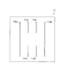
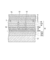
- FIG. 1 is a schematic cross-sectional view showing an example of a light emitting diode of the present invention.
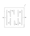
- FIG. 2A is a schematic plan view showing a surface electrode and a current interrupting portion of the light emitting diode shown in FIG. 2B is a schematic plan view showing an ohmic electrode of the light emitting diode shown in FIG.
- FIG. 2C is a schematic plan view showing an ohmic contact electrode of the light emitting diode shown in FIG. 2D is a schematic plan view illustrating the surface electrode, the current blocking unit, the ohmic electrode, and the ohmic contact electrode of the light emitting diode illustrated in FIG.
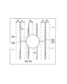
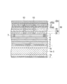
- FIG. 3 is a schematic cross-sectional view showing an example in which a Ge substrate is used as a substrate in the light emitting diode of the present invention.
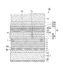
- FIG. 4 is a schematic cross-sectional view showing another example of the light emitting diode of the present invention.
- FIG. 5A to FIG. 5C are schematic cross-sectional views of a part of the metal substrate for explaining the manufacturing process of the metal substrate.
- 6 is a schematic cross-sectional view for explaining one step of the method of manufacturing the light-emitting diode shown in FIG. 1, and is a cross-sectional view at a position corresponding to the cross-sectional view shown in FIG. 7A is a schematic cross-sectional view for explaining one step of the method of manufacturing the light-emitting diode shown in FIG.
- FIG. 7B is a schematic cross-sectional view for explaining one step of the method of manufacturing the light-emitting diode shown in FIG. 1, and is a cross-sectional view at a position corresponding to the cross-sectional view shown in FIG.
- FIG. 8 is a schematic cross-sectional view for explaining one step of the manufacturing method of the light-emitting diode shown in FIG. 1, and is a cross-sectional view at a position corresponding to the cross-sectional view shown in FIG.
- FIG. 9 is a schematic cross-sectional view for explaining one step of the method of manufacturing the light-emitting diode shown in FIG.
- FIG. 10 is a schematic cross-sectional view for explaining one step of the manufacturing method of the light-emitting diode shown in FIG. 1, and is a cross-sectional view at a position corresponding to the cross-sectional view shown in FIG.
- FIG. 11 is a schematic cross-sectional view for explaining one step of the method of manufacturing the light-emitting diode shown in FIG. 1, and is a cross-sectional view at a position corresponding to the cross-sectional view shown in FIG.
- FIG. 12 is a schematic cross-sectional view showing another example of the light emitting diode of the present invention.
- FIG. 1 is a schematic cross-sectional view showing an example of a light emitting diode of the present invention.
- FIG. 2A is a schematic plan view showing a surface electrode and a current interrupting portion of the light emitting diode shown in FIG.
- FIG. 1 is a cross-sectional view corresponding to the line AA ′ shown in FIG. 2A.
- the light emitting diode 100 of this embodiment includes a metal substrate 1 (substrate), a compound semiconductor layer 10 including a light emitting layer 24, an ohmic contact electrode 7, an ohmic electrode 11, a surface electrode 12, and a current blocking unit 13. I have.
- a bonding layer 4, a barrier layer 5, and a reflective layer 6 are provided in this order from the metal substrate 1 side between the metal substrate 1 and the compound semiconductor layer 10.
- the ohmic contact electrode 7 shown in FIG. 1 is made of a plurality of dot-like conductive members in plan view, and a transparent film 8 is filled between the ohmic contact electrodes 7.
- the light-emitting diode shown in FIG. 1 is an example in which a metal substrate is used as a substrate, but in the present invention, a substrate made of a material having a thermal expansion coefficient close to that of a growth substrate can be used without being limited to a metal substrate.
- the light-emitting diode of the present invention is manufactured by forming a compound semiconductor layer including a light-emitting layer on a growth substrate and then replacing (bonding) the growth substrate with another substrate (bonding substrate). However, if the substrate (bonding substrate) has a thermal expansion coefficient significantly different from that of the growth substrate, the positional deviation between the current blocking portion formed before bonding and the pad portion formed after bonding becomes large.
- Is preferably made of a material having a thermal expansion coefficient close to that of the growth substrate.
- the difference in thermal expansion coefficient between the growth substrate and the bonding substrate is , ⁇ 1.5 ppm / K is preferable.
- a substrate normally used as a growth substrate for example, a GaAs substrate (thermal expansion coefficient: 6.0 ppm / K)
- a Ge substrate thermal expansion coefficient: 5.5 ppm / K
- the light emitting diode 100 has a metal protection having resistance against an etchant that covers a plurality of (three layers in the present embodiment) metal layers 1a, 1b, and 1b, and an upper surface 1ba and a lower surface 1bb as a substrate.
- a metal substrate 1 composed of a film 2 is provided.
- the side surface of the metal substrate 1 is preferably covered with a metal protective film 2. Since the metal protective film 2 is resistant to the etchant, corrosion of the metal substrate can be suppressed during etching using the etchant that removes the growth substrate of the compound semiconductor layer 10 including the light emitting layer 24.
- a metal substrate that is not covered with the metal protective film 2 can also be used.
- the thickness of the metal substrate 1 is preferably 50 ⁇ m or more and 150 ⁇ m or less. When the thickness of the metal substrate 1 is thicker than 150 ⁇ m, the manufacturing cost of the light emitting diode 100 increases, which is not preferable. In addition, when the thickness of the metal substrate 1 is less than 50 ⁇ m, cracks, hooks, warping, etc. easily occur during handling of the metal substrate 1, which may reduce the manufacturing yield.
- the plurality of metal layers of the metal substrate 1 are preferably formed by alternately laminating first metal layers and second metal layers.
- the number of the first metal layer and the second metal layer in the metal substrate 1 is preferably 3 to 9 layers including the first metal layer and the second metal layer, preferably 3 to 5 layers. More preferably.
- the number of the first metal layer and the second metal layer is two, the thermal expansion in the thickness direction becomes unbalanced, and the warp of the metal substrate 1 occurs.
- the total number of the first metal layer and the second metal layer is more than nine, it is necessary to reduce the thickness of each of the first metal layer and the second metal layer. .
- the number of the first metal layer and the second metal layer in the metal substrate 1 is an odd number in total.
- the outermost metal layer is preferably made of the same metal material. In this case, for example, when etching a portion corresponding to the planned cutting line of the metal substrate 1 from the outside, the outermost metal layers on the front and back surfaces can be removed by wet etching using the same etchant, which is preferable.
- the first metal layer is disposed in the outermost layer when the number of metal layers is an odd number (in the metal substrate 1 shown in FIG. 1, the first metal layer is indicated by reference numeral 1 b in this embodiment).
- the first metal layer is preferably made of a material having at least a larger thermal expansion coefficient than that of the compound semiconductor layer 10.
- the first metal layer is preferably made of a material having at least a smaller thermal expansion coefficient than that of the compound semiconductor layer 10.
- the first metal layer is made of aluminum, copper, silver, gold, nickel, or an alloy thereof, the heat dissipation is excellent, and cracking of the substrate during bonding can be further suppressed, and a high voltage is applied. Thus, light can be emitted with high brightness.
- the thickness of the first metal layer is preferably 5 ⁇ m or more and 50 ⁇ m or less, and more preferably 5 ⁇ m or more and 20 ⁇ m or less.
- the layer thickness of the first metal layer and the layer thickness of the second metal layer may be different.
- the layer thickness of each layer may be different.
- the total thickness of the first metal layer is preferably 5% or more and 50% or less of the thickness of the metal substrate 1, more preferably 10% or more and 30% or less, and 15% or more and 25% or less. More preferably.
- the total thickness of the first metal layer is less than 5% of the thickness of the metal substrate 1, the effect of increasing the thermal expansion coefficient of the first metal layer is reduced, and the heat sink function is lowered.
- the thickness of the first metal layer exceeds 50% of the thickness of the metal substrate 1, cracking of the metal substrate 1 due to heat when the metal substrate 1 is connected to the compound semiconductor layer 10 cannot be suppressed. .
- a large difference in thermal expansion coefficient between the first metal layer and the compound semiconductor layer 10 may cause cracking of the metal substrate 1 due to heat, resulting in a bonding failure.
- the total thickness of copper is preferably 5% to 40% of the thickness of the metal substrate 1, and is preferably 10% to 30%. More preferably, it is 15% or more and 25% or less.
- the layer thickness of the first metal layer is preferably 5 ⁇ m or more and 30 ⁇ m or less, and more preferably 5 ⁇ m or more and 20 ⁇ m or less.
- the second metal layer is disposed on the inner side when the number of metal layers is an odd number (in the metal substrate 1 shown in FIG. 1, the second metal layer is indicated by reference numeral 1 a in the present embodiment).
- the second metal layer is preferably made of a material having a thermal expansion coefficient smaller than that of the compound semiconductor layer 10. .
- the second metal layer is made of a material having a thermal expansion coefficient larger than that of the compound semiconductor layer 10. Is preferred.
- the material of the second metal layer is preferably a material having a thermal expansion coefficient that is within ⁇ 1.5 ppm / K of the thermal expansion coefficient of the compound semiconductor layer 10.
- the heat dissipation is excellent, and the crack of the metal substrate 1 when the compound semiconductor layer 10 and the metal substrate 1 are bonded can be further suppressed.
- molybdenum 5.1 ppm / K
- tungsten thermal coefficient
- expansion coefficient 4.3 ppm / K
- chromium 4.9 ppm / K)
- Metal protective film As the material of the metal protective film 2, copper, silver, nickel, chromium, platinum, gold or the like can be used, and at least one of chromium or nickel having excellent adhesion and chemically stable platinum or gold is used. A metal film containing at least one of them is preferably used, and a laminated film in which a nickel film having good adhesion to the metal layer and a gold film having excellent chemical resistance are laminated in order from the metal layer side is optimal.
- the thickness of the metal protective film 2 is not particularly limited, but it is 0.2 to 5 ⁇ m, preferably 0.5 to 3 ⁇ m, in an appropriate range from the balance between the resistance to the etchant and the cost. In the case of expensive gold, the thickness is desirably 2 ⁇ m or less.
- the light emitting diode 100 of this embodiment is obtained by bonding a metal substrate 1 to a compound semiconductor layer 10 including a light emitting layer 24.
- the metal substrate 1 includes a plurality of metal layers, and upper and lower surfaces of the plurality of metal layers.
- the metal protective film 2 covers the metal, so that it has excellent heat dissipation, can be driven with a large current to emit high luminance light, and is grown by etching after the metal substrate 1 is bonded to the compound semiconductor layer 10. In the step of removing the substrate for use, the metal substrate 1 is hardly deteriorated.
- the first metal layer and the second metal layer are alternately stacked, and one of the first metal layer and the second metal layer.
- the coefficient of thermal expansion of the entire metal substrate is the heat of the compound semiconductor layer. Since it becomes a thing close
- the first metal layer is made of copper
- the second metal layer is made of molybdenum
- the number of layers of the first metal layer and the second metal layer is the number of layers. 3 and 9 or less, it is excellent in heat dissipation, and can further suppress the cracking of the metal substrate 1 when the compound semiconductor layer 10 and the metal substrate 1 are joined, and can increase the high voltage.
- light can be emitted with high brightness.
- molybdenum having high mechanical strength is sandwiched between copper that can be easily processed, processing such as cutting is easy, and the light emitting diode 100 with high dimensional accuracy is obtained.
- a eutectic metal layer may be formed on the surface of the metal substrate 1 for die bonding.
- the bonding with the metal substrate 1 that is the bonding surface can be a stable eutectic bonding with electrical contact.
- the bonding layer 4 is a layer for bonding the compound semiconductor layer 10 and the like to the metal substrate 1.
- an Au-based eutectic metal having a low melting point that is chemically stable and extremely strong in bonding with the metal substrate 1 is used.
- the Au-based eutectic metal include eutectic compositions of alloys such as AuGe, AuSn, AuSi, and AuIn.
- the bonding layer 4 it is preferable to use AuSi when the metal protective film 2 of the metal substrate 1 is formed of a Ni film and an Au film in this order from the metal substrate 1 side.
- the barrier layer 5 prevents the metal contained in the metal substrate 1 from diffusing and reacting with the reflective layer 6.
- nickel, titanium, platinum, chromium, tantalum, tungsten, molybdenum, or the like can be used as a material of the barrier layer 5.
- the barrier layer 5 in which two or more kinds of metals are combined may be an alloy layer made of two or more kinds of metals, or may be a laminate formed by laminating two or more kinds of metal films.
- the bonding layer 4 may also serve as the barrier layer 5 by adding the above-described material that can be used for the barrier layer 5 to the material of the bonding layer 4. In this case, it is not necessary to provide the barrier layer 5, and the manufacturing process can be simplified.
- the reflective layer 6 reflects the light from the light emitting layer 24 and improves the light extraction efficiency. Since the reflective layer 6 is provided, the light emitting diode 100 can have higher luminance.
- a metal such as an AgPdCu alloy (APC), gold, copper, silver, aluminum, or an alloy thereof can be used. These materials have high light reflectance, and the light reflectance can be 90% or more.
- the translucent layer 8 is formed so as to fill the space between the dot-like conductive members constituting the ohmic contact electrode 7.
- ITO ITO, SiO 2 , IZO, Si 3 N 4 , TiO 2 , TiN, or the like can be used.
- the compound semiconductor layer 10 includes the light emitting layer 24 and is a compound semiconductor stacked structure formed by stacking a plurality of epitaxially grown layers.
- the compound semiconductor layer 10 for example, an AlGaInP layer or an AlGaInAs layer that has high light emission efficiency and has established a substrate bonding technique can be used.
- the AlGaInP layer is a layer made of a material represented by the general formula (Al X Ga 1-X ) Y In 1-YP (0 ⁇ X ⁇ 1, 0 ⁇ Y ⁇ 1). This composition is determined according to the emission wavelength of the light emitting diode.
- the composition of the constituent material is determined according to the light emission wavelength of the light emitting diodes 100.
- the compound semiconductor layer 10 is an n-type or p-type compound semiconductor, and a pn junction is formed therein.
- AlGaInAs includes AlGaAs, GaInAs, GaAs, and the like. Note that the polarity of the surface of the compound semiconductor layer 10 may be either p-type or n-type.
- the compound semiconductor layer 10 shown in FIG. 1 includes a contact layer 22c, a surface roughened layer 23aa, an etching stop layer 31, a cladding layer 23ab, a light emitting layer 24, a cladding layer 23b, and a current diffusion layer 25.
- the contact layer 22c is a layer for reducing the contact resistance of the ohmic electrode.
- the contact layer 22c can be made of, for example, Si-doped n-type GaAs, have a carrier concentration of 1 ⁇ 10 18 cm ⁇ 3 , and a layer thickness of 0.05 ⁇ m.
- the contact layer 22c has the same shape as the ohmic electrode 11 in plan view. Therefore, as shown in FIG. 1, the surface on which the ohmic electrode 11 and the surface electrode 12 are provided is the surface of the surface roughening layer 23aa.
- the contact layer 22c has the same shape as the ohmic electrode 11 in plan view, but the planar shape of the contact layer 22c is not limited to the example shown in FIG.
- the contact layer 22c may have the same planar shape as the surface roughening layer 23aa.
- the surface on which the ohmic electrode 11 and the surface electrode 12 are provided is the surface of the contact layer 22c.
- the surface roughened layer 23aa is formed by roughening the surface in order to improve the light extraction efficiency.
- the surface roughening layer 23aa is made of, for example, n-type (Al 0.5 Ga 0.5 ) 0.5 In 0.5 P doped with Si, and has a carrier concentration of 3 ⁇ 10 18 cm ⁇ 3 .
- the layer thickness can be 3 ⁇ m.
- the etching stop layer 31 functions as a stopper in etching in which a concave portion penetrating the light emitting layer 24 is formed in the compound semiconductor layer 10 performed when the current blocking portion 13 is formed.
- the material used for the etching stop layer 31 is n-type (Al 0.5 Ga 0.5 ) 0.5 In 0.5 P doped with Si, and n-type (Al 0.7 Ga 0 doped with Si. .3 ) 0.5 As can be used, and can be determined as appropriate according to the conditions for etching the compound semiconductor layer 10.
- the material used for the etching stop layer 31 is, for example, AlGaAs (functions as an etching stop layer regardless of the composition) when a recess penetrating the light emitting layer 24 is wet-etched using hydrochloric acid (may be diluted).
- the Al composition is preferably 0.7 or more), and a recess penetrating the light emitting layer 24 is formed with sulfuric acid / hydrogen peroxide (mixed solution of sulfuric acid and hydrogen peroxide), ammonia.
- excess water a mixed solution of ammonia water and hydrogen peroxide
- it is preferably made of AlGaInP.
- the etching stop layer 31 is preferably an As-based material (for example, AlGaAs).
- the etching stop layer 31 is preferably a P-based material (for example, AlGaInP).
- the etching stop layer can be made of the same material as the surface roughening. In that case, it is preferable to increase the thickness by etching.
- the etching stop layer 31 can be made of the same material as the surface roughening layer 23aa.
- the surface roughened layer 23aa also serves as the etching stop layer 31, and since the etching stop layer 31 can be formed simultaneously with the surface roughened layer 23aa, the etching stop layer 31 and the surface roughened layer 23aa are different. Compared with the case of being made of a material, the productivity is excellent.
- the clad layer 23ab is an element of a double hetero structure.
- the clad layer 23ab is made of, for example, Si-doped n-type Al 0.5 In 0.5 P, has a carrier concentration of 3 ⁇ 10 18 cm ⁇ 3 , and a layer thickness of 0.5 ⁇ m. be able to.
- the light emitting layer 24 is preferably made of any one of AlGaAs, GaInAs, or AlGaInP.
- undoped (Al 0.1 Ga 0.9 ) 0.5 In 0.5 P / (Al 0. 5 Ga 0.5 ) 0.5 In 0.5 P may be a laminated structure of 20 pairs, and the layer thickness may be 0.2 ⁇ m.
- the light emitting layer 24 may have a structure such as a double hetero structure (Double Hetero: DH), a single quantum well structure (Single Quantum Well: SQW), or a multiple quantum well structure (Multi Quantum Well: MQW).
- the double heterostructure is a structure in which carriers responsible for radiative recombination can be confined.
- the quantum well structure has a well layer and two barrier layers sandwiching the well layer.
- the SQW has one well layer, and the MQW has two or more well layers. In order to obtain light emission excellent in monochromaticity from the light emitting layer 24, it is preferable to use an MQW structure as the light emitting layer 24.
- the clad layer 23b is made of, for example, p-type Al 0.5 In 0.5 P doped with Mg, has a carrier concentration of 8 ⁇ 10 17 cm ⁇ 3 , and a layer thickness of 0.5 ⁇ m. be able to.
- the current diffusion layer 25 is made of, for example, a p-type GaP layer doped with Mg, has a carrier concentration of 5 ⁇ 10 18 cm ⁇ 3 , and a layer thickness of 2 ⁇ m.
- the configuration of the compound semiconductor layer 10 is not limited to the structure described above, and may include, for example, a current blocking layer or a current constricting layer for limiting a region through which an element driving current flows. .
- a guide layer may be provided between the cladding layer 23ab and the light emitting layer 24. Further, for example, the contact layer 22c, the etching stop layer 31, and the surface roughening layer 23aa are preferably provided, but may not be provided.
- FIG. 2B is a schematic plan view showing an ohmic electrode of the light emitting diode shown in FIG. 1
- FIG. 2C is a schematic plan view showing an ohmic contact electrode of the light emitting diode shown in FIG. 1
- FIG. 2 is a schematic plan view illustrating a surface electrode, a current blocking portion, an ohmic electrode, and an ohmic contact electrode of the light emitting diode shown in FIG. 2B to 2D are plan views showing regions corresponding to the schematic plan view of FIG. 2A.
- the surface electrode 12 includes a pad portion 12a which is a bonding pad and a linear portion (branch portion) 12b.
- the linear portion 12b is provided so as to cover the surface of the ohmic electrode.
- the pad portion 12a is connected to and integrated with the linear portion 12b.
- the surface electrode 12 is preferably made of a laminate formed by laminating two or more kinds of metal films. Specifically, a stacked body of an Au film, a Ti film, and Au (hereinafter, sometimes referred to as “Au / Ti / Au”. The stacked body of other metal films is also expressed in the same manner). Au / Pt / Au, Au / Cr / Au, Au / Ta / Au, Au / W / Au, Au / Mo / Au, etc. can be used.
- the pad portion 12a has a circular shape in plan view because it is easy to wire bond, but may have a shape other than a circular shape.
- the size of the pad portion 12a can be set to, for example, about 50 to 150 ⁇ m in diameter when the pad portion 12a is circular in plan view.
- two linear portions 12b extend in opposite directions from peripheral ends (peripheral end portions) 12aaa and 12aab across the diameter on a straight line passing through the center of the circular pad portion 12a.
- First straight portions 12baa, 12bab and six second straight portions 12bba, 12bbb, 12bca, 12bcb, 12bcc, 12bcd extending in a direction orthogonal to the first straight portions 12baa, 12bab.
- the linear portion 12b is composed of two first straight portions and six second straight portions, but the first straight portion and the second straight portion
- the number of straight portions is not particularly limited.
- the second straight line portions 12bba and 12bbb are connected to the ends of the first straight line portions 12baa and 12ba opposite to the peripheral ends 12aaa and 12aab, respectively, and are spaced apart from the pad portion 12a.
- the second linear portions 12bca, 12bcb, 12bcc, 12bcd are respectively two circumferential end portions 12aba, 12abb, 12abc on one arc side between the two peripheral end portions 12aaa, 12aab and the other arc side, respectively. , 12abd.
- the two second straight portions 12bca and 12bcb extending from the peripheral end portions 12aba and 12abb and the two second straight portions 12bcc and 12bcd extending from the peripheral end portions 12abc and 12abd are on a straight line.
- the second linear portions 12bba and 12bbb extend in a direction parallel to the extending direction.
- the width of the linear portion 12b is wider than the width to cover the linear portion of the ohmic electrode 11, and can be, for example, about 2 to 20 ⁇ m.
- the width of the linear portion 12b does not have to be the same for all of the first linear portion and the second linear portion, but in order to emit light uniformly, the center of the light emitting diode 100 (circular shape in FIG. 2A). It is preferable that the width of the linear portion 12b at the symmetrical position from the center of the pad portion 12a is the same.
- the ohmic electrode 11 is provided on the opposite side of the compound semiconductor layer 10 from the metal substrate 1, and as shown in FIG. 2B, six linear portions 11 ba, 11 bb, 11 ca are provided. , 11cb, 11cc, 11cd.
- a material for the ohmic electrode an AuGeNi alloy, an AuGe alloy, an AuNiSi alloy, an AuSi alloy, or the like can be used.
- the ohmic electrode 11 is composed of six linear portions as an example, but the number of linear portions is not particularly limited.
- the ohmic electrode 11 is not limited to one having a plurality of linear portions, but has a shape discontinuously arranged under the linear portion 12b of the surface electrode 12, for example, a plurality of dot shapes. There may be.
- the ohmic electrode 11 is formed in a region which does not overlap with the pad portion 12a of the surface electrode 12 in plan view.
- the pad under the pad disposed in the region overlapping the pad portion 12a in the light emitting layer 24 in plan view The light emission intensity in the light emitting layer 24a can be weakened.
- the ohmic electrode 11 is disposed at a position overlapping the pad portion 12a, it is possible to avoid the light emitted from the under-pad light emitting layer 24a being absorbed by the pad portion 12a and lowering the light extraction efficiency. The light extraction efficiency can be improved.
- each of the six linear portions of the ohmic electrode 11 includes six second linear portions 12bba, 12bbb of the linear portion 12b of the surface electrode 12, 12bca, 12bcb, 12bcc, and 12bcd are disposed at positions covered by each. That is, the two long linear portions 11ba and 11bb arranged on the outer side in the plan view are arranged directly below the second linear portions 12bba and 12bbb, respectively, and the four short pieces arranged on the inner side in the plan view.
- the linear portions 11ca, 11cb, 11cc, and 11cd are respectively disposed immediately below the second linear portions 12bca, 12bcb, 12bcc, and 12bcd.
- the width of the linear portion of the ohmic electrode 11 is narrower than the width of the linear portion 12b so as to be covered by the linear portion 12b of the surface electrode 12, and is, for example, about 1 to 10 ⁇ m.
- the widths of the linear portions of the ohmic electrode 11 need not all be the same, but in order to emit light uniformly, a symmetrical position from the center of the light emitting diode 100 (the center of the circular pad portion 12a in FIG. 2A). It is preferable to make the widths of the linear portions in the same.
- the shortest distance between the linear portions 11ca, 11cb, 11cc, 11cd closest to the pad portion 12a of the surface electrode 12 and the pad portion 12a is 5 ⁇ m or more and 100 ⁇ m or less. It is preferable.
- the ohmic contact electrode 7 is provided between the metal substrate 1 and the compound semiconductor layer 10. As shown in FIG. 2C, the ohmic contact electrode 7 has a circular dot shape (dot shape) in plan view. A plurality of conductive members.
- the planar shape of each ohmic contact electrode 7 may be a circular shape, an elliptical shape, a donut shape, a linear shape, or the like.
- an AuBe alloy, an AuZn alloy, or the like can be used as a material for the ohmic contact electrode.
- the dot-shaped conductive members constituting the ohmic contact electrode 7 are arranged at positions that do not overlap the pad portions 12a of the surface electrode 12 in plan view.
- the light emission intensity in the lower light emitting layer 24a can be weakened.
- the ohmic contact electrode 7 when the ohmic contact electrode 7 is disposed at a position overlapping the pad portion 12a, it is possible to avoid the light emitted from the under-pad light emitting layer 24a being absorbed by the pad portion 12a and reducing the light extraction efficiency.
- the light extraction efficiency can be further improved.
- the dot-shaped conductive members constituting the ohmic contact electrode 7 are formed on the intermediate positions between the linear portions of the ohmic electrode 11 and the linear portions at both ends of the ohmic electrode 11.
- 11ba, the outer 11bb, the linear portions 11ba, the position on the the distance d 1, d 3 and comparable distance d 2 is to an intermediate position between the linear portion from 11bb, are arranged in linear arrangement Has been.
- the group 7ba of dot-like conductive members arranged in a straight line is an intermediate between the linear portion 11ba and the linear portion 11ca of the ohmic electrode 11 in plan view. It is arranged on the position. Further, the group of dot-shaped conductive members 7bc arranged in a straight line is disposed on an intermediate position between the linear portion 11ba and the linear portion 11cc of the ohmic electrode 11. Moreover, the group 7bb of dot-shaped conductive members arranged in a straight line is disposed on an intermediate position between the linear portion 11bb and the linear portion 11cb of the ohmic electrode 11 in plan view. The group 7bd of dot-like conductive members arranged in a straight line is disposed on an intermediate position between the linear portion 11bb and the minim portion 11 in plan view.
- the group of dot-shaped conductive members 7 ca arranged in a straight line is disposed on an intermediate position between the linear portion 11 ca and the linear portion 11 cb of the ohmic electrode 11 in plan view.
- the group of dot-like conductive members 7 cb arranged in a straight line is disposed on an intermediate position between the linear portion 11 cc and the linear portion 11 cd of the ohmic electrode 11.
- the distance d 2 is linear region from the linear portion 11ba It is arranged at a position approximately the same as the distances d 1 and d 3 to the intermediate position.
- the group 7ab of linearly aligned dot-like conductive member in plan view, outside the left end of the linear portion 11bb ohmic electrode 11, the distance d 2 is linear region from the linear portion 11bb It is arranged at a position approximately the same as the distances d 1 and d 3 to the intermediate position.
- the distances d 1 and d 3 to the intermediate position between the linear parts of the ohmic electrode 11 and the distance d from the linear parts 11ba and 11bb outside the linear parts 11ba and 11bb at both ends of the ohmic electrode 11 It is preferable that the distances 2 are equal to each other so that the current spreads uniformly.
- the dot-like conductive member constituting the ohmic contact electrode 7 can be, for example, a cylindrical member having a diameter of about 5 to 20 ⁇ m. In the group of dot-like conductive members arranged in a straight line, the distance between adjacent conductive members can be set to about 5 to 50 ⁇ m, for example.
- the shortest distance between the dot-like conductive member of the ohmic contact electrode 7 and the pad portion 12a of the surface electrode 12 is preferably 5 ⁇ m or more and 100 ⁇ m or less.
- the current interrupting unit 13 blocks current supplied to the under-pad light emitting layer 24a disposed in a region of the light emitting layer 24 that overlaps the pad portion 12a in plan view. As shown in FIG. 1, the current interrupting unit 13 is provided between the light emitting layer 24 disposed in a region excluding the region overlapping the pad unit 12a in plan view and the under pad light emitting layer 24a.
- the current blocking unit 13 is formed through the cladding layer 23 ab, the light emitting layer 24, the cladding layer 23 b, and the current diffusion layer 25 of the compound semiconductor layer 10, and is integrated with the light transmitting layer 8. It has become. Further, as shown in FIGS. 1, 2A and 2D, the current interrupting part 13 is concentric with the pad part 12a in a plan view, and is annularly arranged in a plan view so as to surround the under-pad light emitting layer 24a. Preferably it is. As a result, the current supplied to the underpad light emitting layer 24a can be more effectively prevented.
- the current interrupting unit 13 is arranged in an annular shape in plan view so as to surround the under-pad light emitting layer 24 a
- the planar shape of 13 is not limited to the example shown in FIG. 2A.
- the current interrupting portion 13 is disposed in a position overlapping the edge of the pad portion 12a in plan view, and the pad portion in plan view.
- An insulating material is embedded in a groove (concave portion) that is disposed on the outer side of 12a and is surrounded by an outer wall 13b that is disposed substantially parallel to the inner wall 13a.
- one end surface 13 c in the thickness direction of the light emitting diode 100 of the current interrupting unit 13 is in contact with the etching stop layer 31, and the other end surface 13 d is on the compound semiconductor layer 10 side of the light transmitting layer 8. It touches the surface.
- the distance between the inner wall 13a and the outer wall 13b is not particularly limited, but the light emitting layer 24 disposed in a region excluding the region overlapping the pad portion 12a in plan view and the pad light emitting layer 24a can be effectively insulated. At the same time, it is preferably 1 ⁇ m or more and more preferably 5 ⁇ m or more so that an insulating material can be easily filled between the inner wall 13a and the outer wall 13b. Further, in order to ensure a sufficient luminance by securing a flat area of the light emitting layer 24 disposed in a region excluding a region overlapping with the pad portion 12a in plan view, a distance between the inner wall 13a and the inner wall 13a. (Spacing between innermost walls of the annular recess: equivalent to the diameter of the under-pad light emitting layer 24a) is preferably 50 ⁇ m or less, and more preferably 10 ⁇ m or less.
- the insulating material used for the current interrupting portion 13 is not particularly limited as long as it can insulate the light emitting layer 24 disposed in the region excluding the region overlapping the pad portion 12a in plan view and the light emitting layer 24a under the pad.
- SiO 2 , Si 3 N 4 , TiO 2 , and TiN can be used.
- the insulating material used for the current interrupting unit 13 has a light transmitting property.
- the current interrupting part 13 can be formed simultaneously with the light-transmitting layer 8 and the productivity is excellent.
- the current interrupting portion 13 is described as an example in which an insulating material is embedded, but the current interrupting portion may be a space. Even when the current interrupting portion is a space, the light emitting layer 24 disposed in a region excluding the region overlapping the pad portion 12a in plan view and the under pad light emitting layer 24a can be insulated, and the under pad light emitting layer The current supplied to 24a can be prevented. Therefore, even when the current interrupting part is made of a space, the light emission intensity immediately below the pad part 12a can be reduced, and the light absorbed by the pad part 12a can be reduced.
- the interval between the inner wall 13a and the outer wall 13b is such that the light emitting layer 24 disposed in a region excluding the region overlapping the pad portion 12a in plan view, and the light emitting layer under the pad In order to effectively insulate from 24a, it is preferably 0.1 ⁇ m or more, and more preferably 1 ⁇ m or more.
- the light emitting layer 24 disposed in a region excluding the region overlapping the pad portion 12a in plan view has a sufficient plane area so that sufficient luminance can be obtained, and the strength of the light emitting diode 100 due to the space.
- the distance between the inner wall 13a and the inner wall 13a is preferably 30 ⁇ m or less, and more preferably 10 ⁇ m or less.
- the current blocking unit 13 is provided between the light emitting layer 24 disposed in a region excluding the region overlapping the pad portion 12a in plan view and the underpad light emitting layer 24a, the underpad light emission.
- the current supplied to layer 24a is interrupted.
- the light emission intensity in the under-pad light emitting layer 24a can be weakened, and a decrease in light extraction efficiency due to the light emitted from the under-pad light emitting layer 24a being absorbed by the pad portion 12a can be avoided. Therefore, according to the light emitting diode 100 of the present embodiment, excellent light extraction efficiency can be obtained.
- FIG. 3 is a schematic cross-sectional view of an example in which the bonding substrate is a Ge substrate 41 in the light emitting diode of the first embodiment.
- the light emitting diode 200 shown in FIG. 3 is different from the light emitting diode 100 shown in FIG. 1 in that a Ge substrate 41 is provided.
- a metal layer (for example, Pt layer) 42 having good adhesion to Ge is provided on the upper and lower surfaces of the Ge substrate 41, and the upper and lower surfaces of the metal layer 42 are excellent in chemical resistance.
- a metal layer (for example, Au layer) 43 is provided.
- a metal layer 42 and a metal layer 43 are sequentially formed on the upper surface of the Ge substrate 41, and then a Ge substrate is formed on the ohmic contact electrode 7 side (on the bonding layer 4) of the compound semiconductor layer 10. 41 is joined. Thereafter, a metal layer 42 and a metal layer 43 are sequentially formed on the lower surface of the Ge substrate 41.
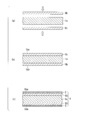
- FIG. 5A to FIG. 5C are schematic cross-sectional views of a part of the metal substrate for explaining the manufacturing process of the metal substrate.
- the metal substrate 1 for example, the first metal layer 1 b whose thermal expansion coefficient is larger than the material of the compound semiconductor layer 10, and the second metal layer 1 b whose thermal expansion coefficient is smaller than the material of the compound semiconductor layer 10, And using a method of hot pressing.
- first metal layers 1b and one substantially flat plate-like second metal layer 1a are prepared.
- a Cu layer having a thickness of 10 ⁇ m is used as the first metal layer 1b
- a Mo layer having a thickness of 75 ⁇ m is used as the second metal layer 1a.
- a single second metal layer 1a is disposed between the two first metal layers 1b to form a laminate.
- a laminated body composed of two first metal layers 1b and one second metal layer 1a is placed in a predetermined pressurizing device, and the first metal layer 1b and the second metal layer 1b are heated at a high temperature.
- a load is applied to the metal layer 1a in the direction of the arrow shown in FIG.
- the first metal layer 1b is a Cu layer
- the second metal layer 1a is a Mo layer
- Such a metal substrate has a thermal expansion coefficient of about 5.7 ppm / K and a thermal conductivity of about 220 W / m ⁇ K.
- the metal protective film 2 is formed on the entire surface of the metal substrate shown in FIG.
- the side surface covered by the metal protective film 2 is the outer peripheral side surface of the metal substrate (plate). . Therefore, when covering the side surface of the metal substrate 1 of each light-emitting diode after separation into pieces with the metal protective film 2, a step of covering the side surface with the metal protective film 2 is performed separately.
- FIG. 5C shows a part of the metal substrate (plate) that is not on the outer peripheral end side, and FIG. 5C does not show the metal protective film on the outer peripheral side surface.
- the metal protective film 2 can be formed using a known film forming method, and it is most preferable to use a plating method capable of forming a film on the entire surface including the side surfaces.
- a plating method it is convenient and desirable to use an electroless plating method in which known techniques and chemicals can be used and no electrode is required.
- the metal substrate shown in FIG. 5 (b) is plated with nickel using an electroless plating method, and then plated with gold, whereby the upper surface, side surfaces, and lower surface of the metal substrate are made of a nickel film and a gold film.
- the metal substrate 1 covered with the protective film 2 can be produced.
- the metal protective film 2 is formed using the electroless plating method
- a known metal such as copper, silver, nickel, chromium, platinum, or gold can be used as the material of the metal protective film 2, but nickel having good adhesion and It is preferable to combine with gold having excellent chemical resistance.
- ⁇ Step of forming compound semiconductor layer> 6 to 10 are schematic cross-sectional views for explaining one step of the method for manufacturing the light-emitting diode shown in FIG. 1, and are cross-sectional views at positions corresponding to the cross-sectional view shown in FIG.
- a semiconductor substrate (growth substrate) 21 is prepared, and an epitaxial multilayer 30 is formed on the semiconductor substrate 21.
- the semiconductor substrate 21 is for forming the epitaxial laminated body 30 shown in FIG.
- the semiconductor substrate 21 for example, a Si-doped n-type GaAs single crystal substrate whose one surface 21 a is inclined by 15 ° from the (100) plane can be used.
- a gallium arsenide (GaAs) single crystal substrate can be used as the semiconductor substrate (growth substrate) 21.
- an epitaxial stacked body 30 including the compound semiconductor layer 10 is formed by growing a plurality of epitaxial layers on one surface 21 a of the semiconductor substrate (growth substrate) 21.
- a method for forming the compound semiconductor layer 10 a metal organic chemical vapor deposition (MOCVD) method, a molecular beam epitaxy (MBE) method, or a liquid phase epitaxy (liquid phase epitaxy) method is used. Etc. can be used.
- the low pressure MOCVD method using trimethylaluminum ((CH 3 ) 3 Al), trimethylgallium ((CH 3 ) 3 Ga), and trimethylindium ((CH 3 ) 3 In) as group III constituent elements are used to epitaxially grow the layers constituting the epitaxial multilayer 30.
- Biscyclopentadienylmagnesium ((C 5 H 5 ) 2 Mg) can be used as the Mg doping material.
- disilane (Si 2 H 6 ) can be used as a Si doping raw material.
- phosphine (PH 3 ) or arsine (AsH 3 ) can be used as a group V constituent element material.
- the temperature at which the epitaxial multilayer 30 is grown is, for example, 750 ° C. when the current diffusion layer 25 is grown, and is 730 ° C. when other epitaxial layers are grown. be able to.
- a buffer layer 22 a made of n-type GaAs doped with Si is formed on one surface 21 a of the semiconductor substrate 21.
- the buffer layer 22a for example, it is preferable to use n-type GaAs doped with Si, have a carrier concentration of about 2 ⁇ 10 18 cm ⁇ 3 , and a layer thickness of about 0.2 to 0.5 ⁇ m.
- the substrate etching stop layer 22b made of Si-doped n-type (Al 0.5 Ga 0.5 ) 0.5 In 0.5 P is formed on the buffer layer 22a.
- the substrate etching stop layer 22b is a layer for preventing the surface roughening layer 23aa from being etched when the semiconductor substrate 21 is removed by etching.
- the substrate etching stop layer 22b preferably has a carrier concentration of about 1 ⁇ 10 18 cm ⁇ 3 and a layer thickness of about 0.5 ⁇ m.
- a contact layer 22c made of Si-doped n-type GaAs is formed on the substrate etching stop layer 22b.
- a surface roughening layer 23aa made of n-type (Al 0.5 Ga 0.5 ) 0.5 In 0.5 P doped with Si is formed on the contact layer 22c.
- the contact layer 22c preferably has a carrier concentration of about 1 ⁇ 10 18 cm ⁇ 3 and a layer thickness of about 0.05 ⁇ m.
- an etching stop layer 31 made of n-type Al 0.7 Ga 0.3 As doped with Si is formed on the surface roughened layer 23aa.
- the etching stop layer 31 preferably has a carrier concentration of about 1 ⁇ 10 18 cm ⁇ 3 and a layer thickness of about 1.0 ⁇ m.
- a cladding layer 23ab made of n-type Al 0.5 In 0.5 P doped with Si is formed on the etching stop layer 31.
- the clad layer 23ab preferably has a thickness of about 0.5 ⁇ m.
- the upper cladding layer 23ab for example, of the order of undoped layer thickness 0.005 ⁇ m (Al 0.1 Ga 0.9) 0.5 In 0.5 and the well layer made of P, undoped layer thickness 0.
- Light emission having a laminated structure of 20 well layers and 19 barrier layers, in which barrier layers made of (Al 0.7 Ga 0.3 ) 0.5 In 0.5 P of about 005 ⁇ m are alternately laminated.
- Layer 24 is deposited.
- a cladding layer 23b made of p-type Al 0.5 In 0.5 P doped with Mg is formed on the light emitting layer 24.
- the clad layer 23b preferably has a thickness of about 0.5 ⁇ m.
- a Mg-doped p-type GaP film having a thickness of about 3 ⁇ m is formed on the clad layer 23b and mirror-polished to a depth of 1 to 2 ⁇ m from the surface.
- the current diffusion layer 25 having a surface roughness of the surface 25a opposite to the semiconductor substrate 21 within 0.18 nm, for example, is obtained.
- the current blocking unit 13 including a recess penetrating the light emitting layer 24 is provided around the pad unit 12a in plan view of the compound semiconductor layer 10.
- a part of the compound semiconductor layer 10 is etched in a groove (concave portion) that is substantially circular in plan view and whose bottom surface 130 a reaches the etching stop layer 31.
- it is provided so as to surround the under-pad light emitting layer 24a.
- a space 130 (concave portion) is formed between the underpad light emitting layer 24a and the light emitting layer 24 disposed in a region excluding a region overlapping the pad portion 12a in plan view.
- both a dry etching method capable of controlling the planar shape with high accuracy and a wet etching method capable of controlling the depth direction with high accuracy are performed.
- a resist layer is selectively formed in a region other than a region that becomes a space in plan view using a photolithography technique, for example, dry etching using SiCl 4 as an etching gas under a bias of 50 W and 10 min. Etch by 2 to 4 ⁇ m by the method.
- hydrochloric acid diluted by 1: 1 is etched to the etching stop layer by a wet etching method at 40 ° C.
- the dry etching method is finished before reaching a predetermined depth by etching in a vertical direction with high accuracy to a predetermined shape in a plan view, and thereafter, an etching stop layer is formed by a wet etching method.
- Etching is performed until it reaches a recess having a predetermined depth. Therefore, in this embodiment, the space 130 having a predetermined planar shape and depth dimension can be formed with high accuracy. For example, when only the dry etching method is performed, the depth of the groove may become deeper than necessary. In addition, when only the wet etching method is performed, the accuracy of the planar shape may be lowered.
- the inner wall 13a of the space 130 is disposed at a position overlapping the edge of the pad portion 12a in plan view, and the outer wall 13b of the space 130 is padded in plan view.
- the inner wall 13a and the outer wall 13b of the space 130 are arranged concentrically with the pad portion 12a in plan view.
- an insulating material is embedded in the space 130 thus obtained.
- the SiO 2 film is formed on the entire surface of the current diffusion layer 25 by using, for example, the CVD method, thereby forming the translucent layer 8 and simultaneously forming the translucent layer 8 in the space 130.
- the current interrupting part 13 is formed by embedding an insulating material.
- a space 130 is formed between the light emitting layer 24 disposed in a region excluding the region overlapping the pad portion 12a in plan view and the pad light emitting layer 24a, and an insulating material is formed in the space 130.
- the case where the current interrupting part 13 is provided by embedding is described as an example. However, when the current interrupting part 13 includes the space 130, it is not necessary to embed an insulating material in the space 130. This is preferable because the manufacturing process can be simplified as compared with the case where an insulating material is embedded in the space 130.
- the current interrupting part 13 is formed before the metal substrate 1 and the compound semiconductor layer 10 are joined.
- the current blocking portion is formed after the metal substrate 1 and the compound semiconductor layer 10 are joined, in the step of forming the current blocking portion, the surface of the compound semiconductor layer 10 opposite to the metal substrate 1 is used. It is necessary to form a space by etching toward the metal substrate 1. For this reason, there exists a possibility that a reflection layer may be exposed by the etching for forming space. If the reflective layer is exposed, the metal that is the material of the reflective layer adheres to the inner surface of the space, and the current may leak.
- the current blocking portion 13 is formed before the metal substrate 1 and the compound semiconductor layer 10 are joined, the reflective layer is not exposed by etching for forming a space, and is easy.
- the current interrupting part 13 can be formed.
- the ohmic contact electrode 7 is formed on the current diffusion layer 25 made of a p-type GaP layer.
- the light transmitting layer 8 through which the ohmic contact electrode 7 penetrates is formed on the compound semiconductor layer 10.
- a plurality of through holes for embedding a conductive member constituting the ohmic contact electrode 7 are formed in the light transmitting layer 8 by using a photolithography technique and an etching technique.
- a photoresist pattern having holes corresponding to the above-described through holes is formed on the light transmitting layer 8, and the light transmitting layer 8 corresponding to the through holes is formed using a hydrofluoric acid-based etchant.
- a plurality of through holes are formed in the translucent layer 8 by removing.
- the plurality of through holes formed in the light transmissive layer 8 are formed at positions corresponding to the positions of the ohmic contact electrodes 7 shown in FIG. That is, the plurality of through holes are positions that do not overlap with the pad portion 12a of the surface electrode 12 formed in the subsequent process in plan view, and are intermediate positions between the linear portions of the ohmic electrode 11 formed in the subsequent process. on, or both ends of the linear portions 11ba ohmic electrode 11, the outer 11bb, the linear portions 11ba, the position of the same degree as the distance d 1 to the intermediate position of the distance d 2 is linear site from 11bb And are arranged in a straight line.
- the ohmic contact electrode 7 is formed on the compound semiconductor layer 10 as shown in FIG. 7B by filling the plurality of through holes of the light transmitting layer 8 with an AuBe alloy by using, for example, a vapor deposition method.
- the reflective layer 6 is formed on the ohmic contact electrode 7 and the translucent layer 8.
- the reflective layer 6 made of APC or Au is formed on the ohmic contact electrode 7 and the light transmitting layer 8 by vapor deposition.
- the barrier layer 5 is formed on the reflective layer 6.
- the barrier layer 5 made of a nickel film, a Ti film, or the like is formed on the reflective layer 6 by vapor deposition.
- the bonding layer 4 is formed on the barrier layer 5.
- the bonding layer 4 made of AuGe which is an Au-based eutectic metal, is formed on the barrier layer 5 by vapor deposition.
- Metal substrate bonding process Next, the metal substrate 1 is bonded to the ohmic contact electrode 7 side of the compound semiconductor layer 10.
- any known technique such as eutectic bonding, diffusion bonding, adhesive, and room temperature bonding may be used.
- the semiconductor substrate 21 on which the epitaxial laminate 30, the reflective layer 6, and the like are formed, and the metal substrate 1 are carried into a decompression device, and a bonding layer is formed on the metal substrate 1.
- the four joint surfaces 4a are arranged so as to face each other.
- the inside of the decompression device is evacuated to 3 ⁇ 10 ⁇ 5 Pa, a load of 500 kg is applied in a state where the stacked semiconductor substrate 21 and the metal substrate 1 are heated to 400 ° C., and the bonding surface 4a of the bonding layer 4 is applied. And the joining surface of the metal substrate 1 are joined to form a joined structure 40.
- the semiconductor substrate 21 and the buffer layer 22 a are selectively removed from the bonded structure 40 with an ammonia-based etchant.
- the resistance to the etchant for removing the semiconductor substrate 21 and the buffer layer 22a is high, and the semiconductor substrate 21 and the buffer layer 22a are removed. This can prevent the quality of the metal substrate 1 from deteriorating.
- the substrate etching stop layer 22b is selectively removed with a hydrochloric acid-based etchant.
- the resistance to the etchant for removing the substrate etching stop layer 22b is high, and the substrate etching stop layer 22b is removed. Therefore, it is possible to prevent the quality of the metal substrate 1 from deteriorating.
- the ohmic electrode 11 is formed on the opposite side of the compound semiconductor layer 10 from the ohmic contact electrode 7. Specifically, for example, an AuGeNi alloy film having a thickness of 0.1 ⁇ m is formed on the entire surface of the contact layer 22c of the compound semiconductor layer 10 using a vapor deposition method, and an AuGeNi alloy film is formed using a photolithography technique and an etching technique.
- the ohmic electrode 11 including the six linear portions 11ba, 11bb, 11ca, 11cb, 11cc, and 11cd shown in FIG. 2B is formed.
- portions of the contact layer 22 c other than the portion overlapping the ohmic electrode 11 in a plan view are replaced with ammonia water (NH 4 OH). It is removed by etching using a mixed solution of hydrogen peroxide (H 2 O 2 and pure water (H 2 O), whereby the planar shape of the contact layer 22c is shown in FIG.
- the planar shape of the ohmic electrode 11 is substantially the same.
- the linear portion 12b is formed so as to cover the surface of the ohmic electrode 11, and the pad portion 12a connected to the linear portion 12b is formed.
- an Au layer having a thickness of 0.3 ⁇ m, a Ti layer having a thickness of 0.3 ⁇ m, and a Ti layer having a thickness of 1 ⁇ m are formed on the entire surface of the compound semiconductor layer 10 on which the ohmic electrode 11 is formed by vapor deposition.
- An Au layer is sequentially formed, and the Au / Ti / Au film is patterned using a photolithography technique and an etching technique.
- the under-pad light emitting layer 24a disposed in a region overlapping with the pad portion 12a in the light emitting layer 24 in a plan view and the region overlapping with the pad portion 12a in a plan view are excluded.
- the pad portion 12a is formed so that the current blocking portion 13 is disposed between the light emitting layer 24 disposed in the region.
- the annular current blocking portion 13 is formed in a plan view in the step of providing the current blocking portion 13
- the step of forming the surface electrode 12 is provided inside the current blocking portion 13 in the plan view.
- the pad portion 12a is formed.
- the surface electrode 12 shown in FIG. 2A including the pad portion 12a and the branch portion 12b connected to the pad portion 12a is formed.
- the plurality of light emitting diodes 100 formed on the metal substrate 1 are separated into pieces. Specifically, for example, there is a method in which each layer formed on the metal substrate 1 to be cut is removed and cut at intervals of 350 ⁇ m using a laser.
- the metal protective film 2 is not formed on the side surface of the metal substrate 1.
- the metal protective film is formed by using a method similar to the method in which the metal protective film 2 is formed on the upper surface and the lower surface of the metal substrate 1 on the side surface of the metal substrate 1 of each individual light-emitting diode 100. 2 may be formed.
- the light emitting diode 100 is disposed in the light emitting layer 24 in a region excluding the pad light emitting layer 24a disposed in the region overlapping the pad portion 12a in plan view and the region overlapping the pad portion 12a in plan view. Since the current blocking part 13 that prevents the current supplied to the under-pad light-emitting layer 24a is provided between the light-emitting layer 24 and the light-emitting intensity immediately below the pad part 12a, the light emission intensity can be reduced. Absorbed light can be reduced. Therefore, the light emitting diode 100 of the present embodiment has excellent light extraction efficiency, and can be suitably used particularly when high luminance light is emitted by a large current drive.
- the current interrupting unit 13 is arranged in an annular shape in plan view so as to surround the under pad light emitting layer 24a, so that the current supplied to the under pad light emitting layer 24a. Can be effectively prevented, the light emission intensity immediately below the pad portion 12a can be further reduced, and the light absorbed by the pad portion 12a can be further reduced.
- the light emitting diode 100 of this embodiment is provided with what the insulating material was embedded as the electric current interruption part 13, compared with the case where an electric current interruption part consists of space, it has the outstanding intensity
- the strength of the light emitting diode 100 can be reduced because the strength of the light emitting diode 100 can be prevented from being reduced due to the current interrupting part 13 being formed.
- the shape of the current interrupting part 13 (space) and the insulating material used for the current interrupting part 13 can be appropriately selected to enhance the insulation of the current interrupting part 13.
- the compound semiconductor layer 10 including the light emitting layer 24 is formed with a recess 130 that penetrates the light emitting layer 24, and an insulating material is embedded in the space 130.
- the under-pad light emitting layer 24a and the pad portion 12a The pad portion 12a is formed so that the current blocking portion 13 is disposed between the light emitting layer 24 disposed in a region excluding the region overlapping in plan view.
- the under-pad light emitting layer 24a is supplied between the under pad light emitting layer 24a and the light emitting layer 24 disposed in a region excluding the region overlapping the pad portion 12a in plan view.
- the light emitting diode 100 having the current blocking part 13 that prevents the current to be generated and having excellent light extraction efficiency can be obtained.
- the annular current blocking unit 13 is formed in plan view, and in the step of forming the surface electrode 12, current blocking is performed in plan view. Since the pad portion 12a is formed inside the portion 13, the current interrupting portion 13 is arranged in an annular shape in plan view so as to surround the under-pad light emitting layer 24a, so that more light absorbed by the pad portion 12a can be obtained. The light emitting diode 100 that can be further reduced is obtained.
- the method for manufacturing the light emitting diode 100 includes the step of forming the etching stop layer 31 on the semiconductor substrate 21 which is a growth substrate before the light emitting layer 24 is formed.
- the etching stop layer 31 By etching the portion using the etching stop layer 31, a method of providing a recess that becomes the space 130, the depth of the recess can be controlled easily and reliably, and an insulating material is embedded in the space 130, The current interrupting part 13 can be formed with high accuracy.
- the current blocking portion 13 is provided in the compound semiconductor layer 10 and the ohmic contact electrode 7 is formed on the compound semiconductor layer 10, and then the ohmic contact electrode 7 of the compound semiconductor layer 10. Since the metal substrate 1 is bonded to the side, the quality of the metal substrate 1 is preferably not deteriorated by the etching for providing the current blocking part 13.
- FIG. 4 is a schematic cross-sectional view showing another example of the light emitting diode of the present invention.
- the light emitting diode 101 shown in FIG. 4 is different from the light emitting diode 100 shown in FIG. For this reason, in this embodiment, only the electric current interruption
- a bonding substrate made of a material having a thermal expansion coefficient close to that of the growth substrate, and a metal substrate including a Ge substrate, a GaP substrate, a GaAs substrate, and a metal substrate with an adjusted thermal expansion coefficient. Etc. can be used.
- the current interrupting part 131 of the light emitting diode 101 includes a reflective layer 133 and a transparent insulating material layer 132 as shown in FIG. As shown in FIG. 4, the transparent insulating material layer 132 is disposed between the reflective layer 133 and the compound semiconductor layer 10.
- the reflective layer 133 shown in FIG. 4 is formed so as to penetrate the light transmitting layer 8 and is integrated with the reflective layer 6.
- the reflective material used for the reflective layer 133 of the electric current interruption part 131 is not specifically limited, It is preferable that a 90% or more high reflectance is obtained. Specifically, for example, Au, Ag, Al, Cu, APC (AgPdCu alloy), or the like can be used.
- the material of the reflective layer 133 of the current interrupting unit 131 is preferably the same as the material of the reflective layer 6. When the material of the reflective layer 133 of the current interrupting part 131 and the material of the reflective layer 6 are the same, the reflective layer 133 can be formed at the same time as the reflective layer 6 and the productivity is excellent.
- the transparent insulating material used for the transparent insulating material layer 132 of the current interrupting part 131 can insulate the under-pad light emitting layer 24a from the light emitting layer 24 disposed in an area excluding the area overlapping the pad part 12a in plan view. Any material can be used as long as it is not particularly limited. For example, SiO 2 , Si 3 N 4 , TiO 2 , or TiN can be used. In addition, the material of the transparent insulating material layer 132 of the current interrupting part 131 is preferably the same as the material of the translucent layer 8.
- the transparent insulating material layer 132 of the current interrupting part 131 and the material of the light transmissive layer 8 are the same, the transparent insulating material layer 132 can be formed at the same time as the light transmissive layer 8, and the productivity is excellent. It will be a thing.
- the thickness of the transparent insulating material layer 132 of the current interrupting part 131 (the interval between the reflective layer 133 and the light emitting layer 24) can be appropriately determined according to the material of the transparent insulating material layer 132 and the material of the reflective layer 133.
- the layer 133 has conductivity, it is preferably 0.05 ⁇ m or more, and more preferably 0.2 ⁇ m or more.
- the distance between the inner wall 13a and the outer wall 13b is The thickness is preferably 0.2 ⁇ m or more, and more preferably 1.0 ⁇ m or more.
- the inner wall (on the inner wall 13a in FIG. 1) is obtained.
- the distance between the inner wall and the inner wall is preferably 30 ⁇ m or less, and more preferably 10 ⁇ m or less.
- the current blocking unit 131 is provided between the under-pad light emitting layer 24a and the light emitting layer 24 arranged in a region excluding the region overlapping the pad portion 12a in plan view, the under-pad light emission The current supplied to layer 24a is blocked.
- the light emission intensity in the under-pad light emitting layer 24a can be weakened, and a decrease in light extraction efficiency due to the light emitted from the under-pad light emitting layer 24a being absorbed by the pad portion 12a can be avoided. Therefore, according to the light emitting diode 101 of the present embodiment, excellent light extraction efficiency can be obtained.
- the current blocking unit 131 since the current blocking unit 131 includes the reflective layer 133 and the transparent insulating material layer 132 disposed between the reflective layer 133 and the compound semiconductor layer 10, the pad portion 12a The light emitted from the light emitting layer 24 disposed in a region excluding the region overlapping in plan view is reflected by the reflective layer 133 of the current blocking unit 131, thereby preventing the light from entering directly below the pad portion 12a. . Therefore, according to the light emitting diode 101 of the present embodiment, further excellent light extraction efficiency can be obtained.
- the bottom surface 130a is an etching stop layer having a substantially annular shape in plan view so as to surround the underpad light emitting layer 24a. Grooves 31 are provided, and a space 130 (concave portion) shown in FIG. 7A is formed between the under-pad light emitting layer 24a and the light emitting layer 24 disposed in a region excluding the region overlapping the pad portion 12a in plan view. .
- a transparent insulating material is deposited on the bottom surface and the inner wall in the space 130 thus obtained.
- a transparent insulating material is formed along the inner wall of the space 130 simultaneously with the formation of the light-transmitting layer 8 by forming a SiO 2 film on the entire surface of the current diffusion layer 25 using, for example, the CVD method.
- Layer 132 is formed.
- the ohmic contact electrode 7 is formed in the same manner as the method for manufacturing the light emitting diode 100 shown in FIG.
- the reflective layer 6 made of APC or Au is formed on the ohmic contact electrode 7 and the translucent layer 8 by using, for example, a vapor deposition method, and at the same time, the transparent insulating material layer 132 is interposed in the space 130 (concave portion).
- the reflective layer 133 is formed in the space 130, and the current blocking portion 131 is formed.
- the light-emitting diode 101 of the present embodiment overlaps the pad-under-light-emitting layer 24a disposed in a region overlapping the pad portion 12a in the light-emitting layer 24 in plan view and the pad portion 12a in plan view. Since the current blocking unit 131 that blocks the current supplied to the underpad light emitting layer 24a is provided between the light emitting layer 24 disposed in a region other than the region, the light emission intensity immediately below the pad unit 12a is weakened. Therefore, the light absorbed by the pad portion 12a can be reduced, and the light extraction efficiency is excellent.
- the current interrupting unit 13 includes the reflective layer 133 and the transparent insulating material layer 132 disposed between the reflective layer 133 and the compound semiconductor layer 10. 133 can block light incident from the light emitting layer 24 directly under the pad portion 12a. As a result, the light absorbed by the pad portion 12a can be further reduced, and a more excellent light extraction efficiency can be obtained.
- the compound semiconductor layer 10 including the light-emitting layer 24 is provided with a recess that penetrates the light-emitting layer 24, thereby forming the space 130 and transparent along the bottom surface and the inner wall of the space 130.
- a step of providing the current blocking unit 13 by forming the insulating material layer 132 and embedding the reflective layer 133 made of a reflective material in the space surrounded by the transparent insulating material layer 132; and the linear portion 12b and the pad portion 12a A step of forming the surface electrode 12 having, and in the step of forming the surface electrode 12, the under-pad light emitting layer 24a and the light emitting layer 24 disposed in a region excluding the region overlapping the pad portion 12a in plan view In this method, the pad portion 12a is formed so that the current interrupting portion 13 is disposed therebetween.
- the under-pad light emitting layer 24a is supplied between the under pad light emitting layer 24a and the light emitting layer 24 disposed in a region excluding the region overlapping the pad portion 12a in plan view.
- the light-emitting diode 101 that includes the current blocking unit 13 that prevents the generated current and has excellent light extraction efficiency can be obtained.
- FIG. 12 is a schematic cross-sectional view showing another example of the light emitting diode of the present invention.
- the light-emitting diode 102 shown in FIG. 12 differs from the light-emitting diode 100 shown in FIG. 1 only in the planar shape of the clad layer 23ab, the light-emitting layer 240, the clad layer 23b, the current diffusion layer 25, and the current blocking portion. It is. For this reason, in this embodiment, only a different point from the light emitting diode 100 shown in FIG. 1 is demonstrated, and the description about another member is abbreviate
- a bonding substrate made of a material having a thermal expansion coefficient close to that of the growth substrate, and a metal substrate including a Ge substrate, a GaP substrate, a GaAs substrate, and a metal substrate with an adjusted thermal expansion coefficient. Etc. can be used.
- a light emitting diode 102 shown in FIG. 12 is a surface electrode 12 including a compound semiconductor layer 10, an ohmic contact electrode 7, an ohmic electrode 11, a linear portion 12b, and a pad portion 12a, similarly to the light emitting diode shown in FIG. And.
- the light-emitting diode 102 shown in FIG. 12 is different from the light-emitting diode 100 shown in FIG. 1 in that the light-emitting layer 240 is not formed in a region overlapping the pad portion 12a in plan view. It is formed only in areas that do not overlap.
- the light emitting diode 102 shown in FIG. 12 is different from the light emitting diode 100 shown in FIG. 1 in that a current blocking portion 231 is formed in a region overlapping the pad portion 12a in plan view.
- the light emitting layer 240 is arrange
- the planar shape of the current interrupting portion 231 is substantially concentric, which is larger than the planar shape of the pad portion 12a.
- the planar shape of the current interrupting portion 231 is that the current interrupting portion 231 is the pad portion 12a. And may be the same as the planar shape of the pad portion 12a, or may be larger or smaller.
- the current interrupting portion 231 includes a filling layer 234, a reflective layer 233, and a transparent insulating material layer 232 as shown in FIG.
- the transparent insulating material layer 232 is disposed between the reflective layer 233 and the compound semiconductor layer 10 as shown in FIG.
- the reflective layer 233 is formed so as to penetrate the light transmitting layer 8 and is integrated with the reflective layer 6.
- the reflective layer 233 has a concave shape having an opening on the metal substrate 1 side, and the filling layer 234 is filled in the concave portion formed of the reflective layer 233. In the example shown in FIG. 12, the filling layer 234 is formed so as to penetrate the reflective layer 6.
- the filling layer 234 may be formed integrally with the reflection layer 233 (in this case, the filling layer 234 is also integrated with the reflection layer 6).
- the reflective material used for the reflective layer 233 of the current interrupting portion 231 is not particularly limited, but preferably has a high reflectance of 90% or more. Specifically, for example, Au, Ag, Al, Cu, APC (AgPdCu alloy), or the like can be used. Moreover, it is preferable that the material of the reflective layer 233 of the current interrupting portion 231 is the same as the material of the reflective layer 6. When the material of the reflective layer 233 and the material of the reflective layer 6 of the current interrupting portion 231 are the same, the reflective layer 233 can be formed at the same time as the reflective layer 6 and the productivity is excellent.
- the transparent insulating material used for the transparent insulating material layer 232 of the current interrupting portion 231 is not particularly limited as long as it can insulate the reflective layer 233 and the compound semiconductor layer 10.
- SiO 2 , Si 3 N 4 , TiO 2 , TiN or the like can be used.
- the material of the transparent insulating material layer 232 of the current interrupting portion 231 is preferably the same as the material of the light transmissive layer 8.
- the transparent insulating material layer 232 of the current interrupting portion 231 and the material of the light transmissive layer 8 are the same, the transparent insulating material layer 232 can be formed at the same time as the light transmissive layer 8, and the productivity is excellent. It will be a thing.
- the filling layer 234 of the current interrupting unit 231 is not particularly limited, but for example, a metal such as SiO 2 , Si 3 N 4 , TiO 2 , TiN or Au, Ag, Al, Cu, APC, Pt, Ni, Ti, or the like is used. be able to. Also, it may be a space.
- a metal such as SiO 2 , Si 3 N 4 , TiO 2 , TiN or Au, Ag, Al, Cu, APC, Pt, Ni, Ti, or the like is used. be able to. Also, it may be a space.
- the current blocking consisting of a space (concave portion) penetrating the light emitting layer 24 immediately below the compound semiconductor layer 10 in plan view is performed by sequentially performing a dry etching method and a wet etching method.
- a portion 231 is provided.
- the concave portion can be formed in the light emitting layer 240 in a region overlapping the pad portion 12a in plan view in the same manner as the method for manufacturing the light emitting diode shown in FIG.
- a transparent insulating material is deposited on the bottom surface and the inner wall in the space.
- a transparent insulating material layer is formed along the inner wall of the space at the same time as forming the translucent layer 8 by forming a SiO 2 film on the entire surface of the current diffusion layer 25 using, for example, a CVD method. 232 is formed.
- the ohmic contact electrode 7 is formed in the same manner as the method for manufacturing the light emitting diode 100 shown in FIG.
- the reflective layer 6 made of APC or Au is formed on the ohmic contact electrode 7 and the translucent layer 8 by using, for example, a vapor deposition method, and at the same time, the space (concave portion) surrounded by the transparent insulating material layer 232 is formed.
- the reflective layer 233 is formed in the space by embedding a metal material to be the reflective layer 233 through the transparent insulating material layer 232.
- the filling layer 234 is formed on the reflective layer 233 so as to fill the space (concave portion), and the current blocking portion 231 is formed.
- the filling layer 234 can be formed by a CVD method or the like using a photoresist having a pattern in which only a filling portion is opened as a mask.
- a plating method can be used.
- the filling layer 234 is formed of the same material as that of the reflective layer 6, the concave layer may be filled with the material simultaneously with the formation of the reflective layer 6.
- the filling layer 234 is a space, the barrier layer 5 and the bonding layer 6 are formed in this order after the reflective layer 233 is formed.
- the light emitting layer 240 is formed only in a region that does not overlap with the pad portion 12a in plan view. Therefore, the light emitting diode 240 does not emit light immediately below the pad portion 12a, and light absorbed by the pad portion 12a. And has excellent light extraction efficiency.
- the light emitting layer 240 is disposed so as to surround the current blocking portion 231 disposed in a region overlapping the pad portion 12a in plan view. It can be easily manufactured by removing the light emitting layer in the region to be the current blocking portion 231 of the layer and forming the current blocking portion 231.
- the compound semiconductor layer 10 including the light emitting layer 240 is provided with a recess that penetrates the light emitting layer 240 to form the space 130 and is transparent along the bottom surface and the inner wall of the space 130.
- a step of forming a current blocking portion 231 by forming an insulating material layer 232 and embedding a reflective layer 233 made of a reflective material in a space surrounded by the transparent insulating material layer 232; a linear portion 12b and a pad portion 12a; Forming the surface electrode 12, and in the step of forming the surface electrode 12, the pad portion 12a is formed in a region overlapping the current interrupting portion 231 in plan view.
- the pad portion 12a is arranged in a region overlapping the current interrupting portion 231 in plan view, only the light emitting layer 240 does not overlap with the pad portion 12a in plan view.
- the light emitting diode 102 having excellent light extraction efficiency is obtained.
- the current blocking portion 231 is provided in the compound semiconductor layer 10 and the ohmic contact electrode 7 is formed on the compound semiconductor layer 10, and then the ohmic contact electrode 7 of the compound semiconductor layer 10. Since the metal substrate 1 is bonded to the side, the quality of the metal substrate 1 is preferably not deteriorated by the etching for providing the current blocking portion 231.
- the light-emitting diode lamp of this embodiment is obtained by mounting (die-bonding) the light-emitting diode of any of the first to third embodiments described above on a mount substrate. Since the light emitting diode lamp of this embodiment is provided with the light emitting diode which has the outstanding light extraction efficiency, it becomes a high-intensity thing.
- the illuminating device of this embodiment has a plurality of light-emitting diode lamps mounted by mounting (die-bonding) the light-emitting diodes of any of the first to third embodiments described above on a mount substrate. Since the lighting device of this embodiment is equipped with a plurality of light emitting diodes having excellent light extraction efficiency, it has high luminance.
- Example 1 The light emitting diode lamp shown in FIG. 1 was produced and evaluated for characteristics.
- ⁇ Manufacturing process of metal substrate> A 75 ⁇ m thick Mo layer (foil, plate) is sandwiched between two 10 ⁇ m thick Cu layers (foil, plate) and thermocompression bonded to form a 95 ⁇ m thick metal plate plate (before cutting into individual pieces). Formed. After polishing the upper surface and the lower surface of the obtained metal plate plate, it was washed with an organic solvent to remove dirt. Next, a 2 ⁇ m Ni film and a 1 ⁇ m Au film are sequentially formed on the entire surface of the metal plate plate as a metal protective film 2 by an electroless plating method to form a metal substrate (metal substrate before cutting into individual pieces) 1.
- a metal substrate metal substrate before cutting into individual pieces
- an epitaxial layer is sequentially stacked on a semiconductor substrate (growth substrate) 21 made of Si-doped n-type GaAs single crystal and having a diameter of 50 mm and a thickness of 350 ⁇ m.
- Epitaxial laminated body 30 was produced.
- the semiconductor substrate 21 has a growth surface that is inclined by 15 ° from the (100) plane in the (0-1-1) direction, and has a carrier concentration of 1 ⁇ 10 18 cm ⁇ 3 .
- contact layer 22c made of Si-doped n-type GaAs
- surface roughened layer 23aa made of Si-doped n-type (Al 0.5 Ga 0.5 ) 0.5 In 0.5 P
- Si Etching stop layer 31 made of doped n-type (Al 0.7 Ga 0.3 ) 0.5 As
- Cladding layer 23b made of Al 0.5 In 0.5 P of p-type doped optical layer 24, Mg, a current diffusion layer 25
- the buffer layer 22a had a carrier concentration of 2 ⁇ 10 18 cm ⁇ 3 and a layer thickness of 0.5 ⁇ m.
- the substrate etching stop layer 22b has a carrier concentration of 1 ⁇ 10 18 cm ⁇ 3 and a layer thickness of 0.5 ⁇ m.
- the contact layer 22c has a carrier concentration of about 1 ⁇ 10 18 cm ⁇ 3 and a layer thickness of 0.05 ⁇ m.
- the surface roughened layer 23aa has a carrier concentration of 1 ⁇ 10 18 cm ⁇ 3 and a layer thickness of 3 ⁇ m.
- the etching stop layer 31 has a carrier concentration of 1 ⁇ 10 18 cm ⁇ 3 and a layer thickness of 1.0 ⁇ m.
- the cladding layer 23ab has a carrier concentration of 2 ⁇ 10 18 cm ⁇ 3 and a layer thickness of 0.5 ⁇ m.
- the well layer and the barrier layer of the light emitting layer 24 are undoped and have a thickness of 5 nm.
- the clad layer 23b had a carrier concentration of 8 ⁇ 10 17 cm ⁇ 3 and a layer thickness of 0.5 ⁇ m.
- the current diffusion layer 25 has a carrier concentration of 5 ⁇ 10 18 cm ⁇ 3 and a layer thickness of 3 ⁇ m.
- the epitaxial laminated body 30 including the compound semiconductor layer 10 was formed on the semiconductor substrate 21 by using a low pressure metal organic chemical vapor deposition (MOCVD) method.
- MOCVD metal organic chemical vapor deposition
- trimethylaluminum ((CH 3 ) 3 Al), trimethylgallium ((CH 3 ) 3 Ga), and trimethylindium ((CH 3 ) 3 In) were used as the raw materials for the group III constituent elements.
- biscyclopentadienyl magnesium bis- (C 5 H 5 ) 2 Mg
- disilane (Si 2 H 6 ) was used as a Si doping material.
- phosphine (PH 3 ) and arsine (AsH 3 ) were used as raw materials for the group V constituent elements.
- the current spreading layer 25 was grown at 750 ° C., and the other layers were grown at 700 ° C.
- the surface 25a opposite to the semiconductor substrate 21 of the current diffusion layer 25 was mirror-polished to a depth of 2 ⁇ m from the surface to make the surface roughness 0.18 nm.
- the inner wall 13a of the space 130 is disposed at a position overlapping the edge of the pad portion 12a in plan view, and the outer wall 13b of the space 130 is disposed substantially parallel to the outer side of the pad portion 12a in plan view, facing the inner wall 13a.
- the inner wall 13a of the space 130 was circular in plan view with a diameter of 100 ⁇ m
- the outer wall 13b was circular in plan view with a diameter of 110 ⁇ m
- the distance between the inner wall 13a and the outer wall 13b was 5 ⁇ m.
- etching for forming the space 130 both a dry etching method and a wet etching method were used. Specifically, a resist layer is selectively formed in a region other than a region that is a space in a plan view using a photolithography technique, and dry etching is performed using SiCl4 as an etching gas under a bias of 50 W and 10 min. Etch 2-4 ⁇ m. Thereafter, hydrochloric acid diluted 1: 1 was etched up to the etching stop layer by a wet etching method at 40 ° C.
- a SiO 2 film is formed on the entire surface of the current diffusion layer 25 by using the CVD method to form the light-transmitting layer 8 having a thickness of 0.3 ⁇ m, and at the same time, an insulating material is embedded in the space 130.
- the current interruption part 13 was formed.
- a plurality of through holes for embedding a conductive member constituting the ohmic contact electrode 7 were formed in the light transmitting layer 8 by using a photolithography technique and an etching technique.
- a plurality of cylindrical ohmic contact electrodes 7 having a height of 0.3 ⁇ m and a diameter of 9 ⁇ m are formed on the compound semiconductor layer 10 by filling the plurality of through-holes of the light-transmitting layer 8 with an AuBe alloy by vapor deposition. Formed.
- the ohmic contact electrode 7 was formed at a position where the shortest distance from the conductive member closest to the pad portion 12a of the surface electrode 12 was 10 ⁇ m.
- a 0.7 ⁇ m-thick reflective layer 6 made of Au was formed on the ohmic contact electrode 7 and the light-transmitting layer 8 by vapor deposition.
- the barrier layer 5 made of a Ti film having a thickness of 0.5 ⁇ m was formed on the reflective layer 6 by vapor deposition.
- the bonding layer 4 made of AuGe and having a thickness of 1.0 ⁇ m was formed on the barrier layer 5 by vapor deposition.
- the semiconductor substrate 21 and the buffer layer 22a are selectively removed from the bonding structure 40 with an ammonia-based etchant, the substrate etching stop layer 22b is selectively removed with a hydrochloric acid-based etchant, and the compound semiconductor layer 10 including the light emitting layer 24 did.
- ⁇ Omic electrode formation process Next, an AuGeNi alloy film having a thickness of 0.1 ⁇ m is formed on the entire surface of the contact layer 22c of the compound semiconductor layer 10 by vapor deposition, and the AuGeNi alloy film is patterned by using a photolithography technique and an etching technique.
- the ohmic electrode 11 including the six linear portions 11ba, 11bb, 11ca, 11cb, 11cc, and 11cd shown in FIG. 2B was formed.
- the widths of the six linear parts were all 4 ⁇ m, the lengths of the linear parts 11ba and 11bb were 270 ⁇ m, and the lengths of the linear parts 11ca, 11cb, 11cc and 11cd were 85 ⁇ m.
- the closest distance between the linear portions 11ba and 11bb and the pad portion 12a of the surface electrode 12 is 45 ⁇ m, and the closest distance between the linear portions 11ca, 11cb, 11cc and 11cd and the pad portion 12a of the surface electrode 12 is 10 ⁇ m. It was.
- the closest distance between the linear portions 11ba and 11bb and the pad portion 12a of the surface electrode 12 is equal to the length of the first straight portions 12baa and 12bab of the surface electrode 12.
- portions of the contact layer 22 c other than the portion overlapping the ohmic electrode 11 in a plan view are replaced with ammonia water (NH 4 OH). It is removed by etching using a mixed solution of hydrogen peroxide (H 2 O 2 and pure water (H 2 O), and the planar shape of the contact layer 22c is substantially the same as the planar shape of the ohmic electrode 11. did.
- the pad portion 12a has a circular shape in a plan view with a diameter of 100 ⁇ m, and is formed inside the current interrupting portion 13 in a plan view.
- the width of the linear portion 12b was 8 ⁇ m for both the first straight portion and the second straight portion.
- the length of the first straight portions 12baa and 12bab is 43 ⁇ m
- the length of the second straight portions 12bba and 12bbb is 270 ⁇ m
- the length of the second straight portions 12bca, 12bcb, 12bcc and 12bcd is 100 ⁇ m. did.
- each layer formed on the metal substrate 1 at a portion to be cut is removed, and a plurality of light emitting diodes 100 formed on the metal substrate 1 are individually cut by cutting into squares at intervals of 350 ⁇ m using a laser. Turned into. Next, the individual light emitting diodes 100 were mounted on a mount substrate to obtain the light emitting diode lamp of Example 1.
- the characteristics of the lamp provided with the light emitting diode 100 of Example 1 shown in FIG. 1 obtained as described above were evaluated as follows. When a current was passed between the ohmic contact electrode 7 and the ohmic electrode 11, red light having a dominant wavelength of 620 nm was emitted.
- the forward voltage (V F ) when a current of 20 milliamperes (mA) is passed through the light emitting diode lamp in the forward direction is 1.95. V.
- the light emission output when the forward current was 20 mA was 9.44 mW.
- Example 2 The light emitting diode lamp 101 shown in FIG. 4 was produced and evaluated for characteristics. First, in the same manner as in the method for manufacturing the light emitting diode 100 of Example 1, the steps up to the step before forming the current interrupting portion 131 were performed. Next, in the step of forming the current interrupting part 131, the space 130 was formed in the same manner as in the method for manufacturing the light emitting diode 100 of Example 1.
- the inner wall 13a of the space 130 is circular in plan view with a diameter of 100 ⁇ m
- the outer wall 13b is circular in plan view with a diameter of 120 ⁇ m
- the distance between the inner wall 13a and the outer wall 13b is 10 ⁇ m.
- an SiO 2 film was formed on the entire surface of the current diffusion layer 25 by using the CVD method, thereby forming the light-transmitting layer 8 and simultaneously forming the transparent insulating material layer 132 along the inner wall of the space 130.
- the inner wall of the space 130 in which the transparent insulating material layer 132 was formed was circular in plan view with a diameter of 101 ⁇ m.
- the ohmic contact electrode 7 was formed in the same manner as in the light emitting diode manufacturing method 100 of Example 1.
- the reflective layer 6 made of Au is formed on the ohmic contact electrode 7 and the light transmitting layer 8 by vapor deposition, and at the same time, the reflective layer 133 is formed in the space 130 in which the transparent insulating material layer 132 is formed. did.
- the characteristics of the lamp provided with the light emitting diode 101 of Example 2 shown in FIG. 4 thus obtained were evaluated as follows.
- a current was passed between the ohmic contact electrode 7 and the ohmic electrode 11, red light having a dominant wavelength of 620 nm was emitted.
- the forward voltage (V F ) when a current of 20 milliamperes (mA) was passed through the light emitting diode lamp in the forward direction was 1.95V.
- the light emission output when the forward current was 20 mA was 9.60 mW.
- Example 3 The steps until the light emitting diodes 100 are separated into pieces are the same as in the method of manufacturing the light emitting diodes 100 according to the first embodiment, except that an insulating material is not embedded in the spaces 130 and the current blocking portions made of spaces are provided. went. Next, each of the separated light emitting diodes was mounted on a mount substrate to obtain a light emitting diode lamp of Example 3.
- the characteristics of the light-emitting diode lamp of Example 3 obtained in this way were evaluated as follows. When a current was passed between the ohmic contact electrode 7 and the ohmic electrode 11, red light having a dominant wavelength of 620 nm was emitted.
- the forward voltage (V F ) when a current of 20 milliamperes (mA) was passed through the light emitting diode lamp in the forward direction was 1.95V.
- the light emission output when the forward current was 20 mA was 9.44 mW.
- Example 4 The light emitting diode lamp 102 shown in FIG. 12 was produced and evaluated for characteristics. First, in the same manner as in the method for manufacturing the light emitting diode 100 of Example 1, the steps before the step of forming the current interrupting portion 231 were performed. In Example 4, the materials and / or thicknesses of the etching stop layer 31, the cladding layer 23ab, the light emitting layer 240, and the cladding layer 23b are different, and the materials and / or thicknesses shown below are used.
- the etching stop layer 31 has a carrier concentration of 1 ⁇ 10 18 cm ⁇ 3 and a layer thickness of 1.0 ⁇ m.
- the barrier layer and well layer of the light emitting layer 240 were undoped and had a layer thickness of 7 nm.
- a recess whose bottom surface reaches the etching stop layer 31 is provided in the same manner as in the method of manufacturing the light emitting diode 100 of Example 1, and the pad portion 12 a of the light emitting layer 240 is viewed in plan view.
- a space was formed in the overlapping area.
- the inner wall of the recess was circular in plan view with a diameter of 100 ⁇ m.
- both the dry etching method and the wet etching method were used for the etching for forming the space.
- a resist layer is selectively formed in a region other than a region that is a space in a plan view using a photolithography technique, and dry etching is performed using SiCl4 as an etching gas under a bias of 50 W and 10 min. Etch 2-4 ⁇ m.
- a mixed solution of sulfuric acid: hydrogen peroxide: water was etched to the etching stop layer by a wet etching method at 30 ° C.
- a SiO 2 film was formed on the entire surface of the current diffusion layer 25 by CVD, thereby forming the light-transmitting layer 8 and simultaneously forming the transparent insulating material layer 232 along the inner wall of the space.
- the inner wall of the space surrounded by the transparent insulating material layer 232 was circular in a plan view with a diameter of 99 ⁇ m.
- an ohmic contact electrode 7 was formed in the same manner as in the light emitting diode manufacturing method of Example 1.
- the reflective layer 6 made of Au was formed on the ohmic contact electrode 7 and the translucent layer 8 by vapor deposition, and at the same time, the reflective layer 233 was formed in the space surrounded by the transparent insulating material layer 232.
- the inner wall of the space surrounded by the transparent insulating material layer 232 and the reflective layer 233 was circular in plan view with a diameter of 98 ⁇ m.
- the current blocking portion 231 was formed by filling the space surrounded by the reflective layer 233 with an insulating material to form the filling layer 234. Thereafter, in the same manner as in the method for manufacturing the light emitting diode 100 of Example 1, the steps until the surface electrode 12 is formed are performed. In the step of forming the surface electrode 12, the pad is formed in the region overlapping the current interrupting portion 231 in plan view. Part 12a was formed. Thereafter, in the same manner as in the method for manufacturing the light emitting diode 100 of Example 1, steps until the light emitting diodes 102 were separated into pieces were performed. Next, each of the separated light emitting diodes 102 was mounted on a mount substrate to obtain a light emitting diode lamp of Example 4.
- the characteristics of the lamp provided with the light emitting diode 102 of Example 4 shown in FIG. 12 thus obtained were evaluated as follows. When a current was passed between the ohmic contact electrode 7 and the ohmic electrode 11, infrared light having a peak wavelength of 850 nm was emitted.
- the forward voltage (V F ) when a current of 20 mA (mA) was passed through the light emitting diode lamp in the forward direction was 1.45V.
- the light emission output when the forward current was 20 mA was 8.40 mW.
- the characteristics of the comparative light-emitting diode lamp thus obtained were evaluated as follows. When a current was passed between the ohmic contact electrode 7 and the ohmic electrode 11, red light having a dominant wavelength of 620 nm was emitted.
- the forward voltage (V F ) when a current of 20 milliamperes (mA) was passed through the light emitting diode lamp in the forward direction was 1.95V.
- the light emission output when the forward current was 20 mA was 8.00 mW.
- the light output efficiency is improved by providing the current blocking unit that blocks the current supplied to the light emitting layer under the pad, and thus the light emission output is improved.
Abstract
Description
本願は、2011年10月25日に、日本に出願された特願2011-234005号に基づき優先権を主張し、その内容をここに援用する。 The present invention relates to a light-emitting diode, a method for manufacturing a light-emitting diode, a light-emitting diode lamp, and a lighting device, and more particularly, a light-emitting diode having excellent light extraction efficiency and a method for manufacturing the same, About.
This application claims priority based on Japanese Patent Application No. 2011-234005 filed in Japan on October 25, 2011, the contents of which are incorporated herein by reference.
例えば、特許文献1には、活性層およびその上側層を貫通して孔部を形成し、この孔部内の活性層およびその上側層を除去した部分に絶縁膜を介してワイヤボンディング部を設け、ワイヤボンディング部を線状電極に接続した半導体発光装置が記載されている。 Some light emitting diodes having such a light emitting layer are provided with a surface electrode comprising a bonding pad and a linear portion connected to the bonding pad on the surface opposite to the substrate.
For example, in
本発明は、上記事情を鑑みてなされたものであり、優れた光取り出し効率が得られる発光ダイオードおよびその製造方法、これを備えた発光ダイオードランプ及び照明装置を提供することを目的とする。 Conventional light emitting diodes are required to further improve the light extraction efficiency. In particular, there is an increasing demand for improving the light extraction efficiency in a light emitting diode that emits light with high brightness by driving with a large current.
The present invention has been made in view of the above circumstances, and an object of the present invention is to provide a light-emitting diode capable of obtaining excellent light extraction efficiency, a method for manufacturing the light-emitting diode, a light-emitting diode lamp and an illumination device including the light-emitting diode.
(3)前記電流遮断部が、空間からなることを特徴とする(1)または(2)に記載の発光ダイオード。 (2) The light-emitting diode according to (1), wherein the current interrupting portion is annularly arranged in a plan view so as to surround the light emitting layer under the pad.
(3) The light-emitting diode according to (1) or (2), wherein the current interrupting unit is a space.
(7)前記電流遮断部が、反射層と、前記反射層と前記化合物半導体層との間に配置された透明絶縁材料層とを含むものであることを特徴とする(1)(2)(4)(5)のいずれかに記載の発光ダイオード。 (6) The light-emitting diode according to any one of (1), (2), (4), and (5), wherein the current interrupting portion is formed by embedding an insulating material.
(7) The current blocking section includes a reflective layer and a transparent insulating material layer disposed between the reflective layer and the compound semiconductor layer. (1) (2) (4) (5) The light emitting diode in any one of.
(9)前記パッド部が、平面視で円形状であることを特徴とする(1)~(8)のいずれかに記載の発光ダイオード。
(10)前記発光層が、AlGaAs、InGaAs、又は、AlGaInPのいずれかからなることを特徴とする前項(1)~(9)のいずれかに記載の発光ダイオード。
(11)前記オーミックコンタクト電極が、前記パッド部と平面視で重ならない領域に形成されていることを特徴とする(1)~(10)のいずれかに記載の発光ダイオード。 (8) The light-emitting diode according to any one of (1) to (7), wherein the substrate is any one of a Ge substrate, a GaP substrate, a GaAs substrate, and a metal substrate.
(9) The light-emitting diode according to any one of (1) to (8), wherein the pad portion has a circular shape in plan view.
(10) The light emitting diode as described in any one of (1) to (9) above, wherein the light emitting layer is made of any one of AlGaAs, InGaAs, and AlGaInP.
(11) The light-emitting diode according to any one of (1) to (10), wherein the ohmic contact electrode is formed in a region that does not overlap the pad portion in plan view.
(13)(1)~(11)のいずれかに記載の発光ダイオードを複数個搭載した照明装置。 (12) A light-emitting diode lamp comprising the light-emitting diode according to any one of (1) to (11).
(13) An illumination device including a plurality of light emitting diodes according to any one of (1) to (11).
(16)前記オーミックコンタクト電極を形成する工程は、前記オーミックコンタクト電極が貫設するように前記化合物半導体層上に透光膜を形成する工程を含み、前記絶縁材料の埋め込みは前記透光膜を形成する工程において前記凹部内に該透光膜を埋め込むことにより行うことを特徴とする(15)に記載の発光ダイオードの製造方法。
(17)前記凹部の底面及び内壁に透明絶縁材料を堆積し、前記凹部に前記透明絶縁材料を介して金属材料を埋め込むことにより前記電流遮断部を形成することを特徴とする(14)に記載の発光ダイオードの製造方法。 (15) The method for manufacturing a light-emitting diode according to (14), wherein the current interrupting portion is formed by embedding an insulating material in the recess.
(16) The step of forming the ohmic contact electrode includes a step of forming a translucent film on the compound semiconductor layer so that the ohmic contact electrode penetrates, and the embedding of the insulating material includes the translucent film (15) The method for producing a light-emitting diode according to (15), wherein the step of forming is performed by embedding the light-transmitting film in the recess.
(17) The current blocking portion is formed by depositing a transparent insulating material on a bottom surface and an inner wall of the concave portion and embedding a metal material in the concave portion through the transparent insulating material. Manufacturing method of the light emitting diode.
(21)前記オーミックコンタクト電極を形成する工程は、前記オーミックコンタクト電極が貫設するように前記化合物半導体層上に透光膜を形成する工程を含み、前記絶縁材料の埋め込みは前記透光膜を形成する工程において前記凹部内に該透光膜を埋め込むことにより行うことを特徴とする(20)に記載の発光ダイオードの製造方法。
(22)前記凹部の底面及び内壁に透明絶縁材料を堆積し、前記凹部に前記透明絶縁材料を介して金属材料を埋め込むことにより前記電流遮断部を形成することを特徴とする(19)に記載の発光ダイオードの製造方法。 (20) The method for manufacturing a light-emitting diode according to (19), wherein the current interrupting portion is formed by embedding an insulating material in the recess.
(21) The step of forming the ohmic contact electrode includes a step of forming a translucent film on the compound semiconductor layer so that the ohmic contact electrode penetrates, and the embedding of the insulating material includes the translucent film (20) The method for producing a light-emitting diode according to (20), wherein the light-transmitting film is embedded in the recess in the forming step.
(22) The current interrupting portion is formed by depositing a transparent insulating material on a bottom surface and an inner wall of the concave portion and embedding a metal material in the concave portion through the transparent insulating material. Manufacturing method of the light emitting diode.
(24)前記凹部の底面及び内壁に透明絶縁材料を堆積し、前記凹部に前記透明絶縁材料を介して金属材料及び絶縁材料を順に埋め込むことにより前記電流遮断部を形成することを特徴とする(19)に記載の発光ダイオードの製造方法。 (23) The step of forming the ohmic contact electrode includes forming a light-transmitting film on the compound semiconductor layer so as to penetrate the ohmic contact electrode, and before performing the step of removing the growth substrate. A step of forming a reflective layer on the light-transmitting film, the transparent insulating material being deposited when the light-transmitting film is formed, and the embedding of the metal material in the step of forming the reflective layer. The manufacturing method of the light emitting diode as described in (22) characterized by performing.
(24) The current blocking part is formed by depositing a transparent insulating material on a bottom surface and an inner wall of the recess, and sequentially embedding a metal material and an insulating material through the transparent insulating material in the recess. The manufacturing method of the light emitting diode as described in 19).
また、ウェットエッチング法では、側面の垂直な凹部を高精度で形成することは困難である。このため、ウェットエッチング法のみで凹部を設けると、所望の深さの凹部を形成するために必要以上に化合物半導体層を除去せざる得なくなるおそれがある。
これに対して、本発明の発光ダイオードの製造方法では、ドライエッチング法により平面視して必要な範囲を高精度で垂直方向にエッチングし、その後、エッチングストップ層を用いるウェットエッチング法により、エッチングストップ層に達するまでエッチングすることにより、所定の平面形状および深さの凹部が高精度で形成される。 More specifically, the dry etching method is an etching method in which it is difficult to form a recess having a desired depth with high accuracy. For this reason, when the recess is provided only by the dry etching method, the dimensional accuracy in the depth direction of the recess becomes insufficient, and the depth of the recess may be too deep.
In addition, it is difficult to form the vertical recesses on the side surfaces with high accuracy by the wet etching method. For this reason, if the recess is provided only by the wet etching method, the compound semiconductor layer may be removed more than necessary in order to form the recess having a desired depth.
In contrast, in the method of manufacturing a light emitting diode according to the present invention, a necessary range is etched in a vertical direction with high accuracy in plan view by a dry etching method, and then etching stop is performed by a wet etching method using an etching stop layer. By etching until reaching the layer, a recess having a predetermined planar shape and depth is formed with high accuracy.
〔発光ダイオード〕
図1は、本発明の発光ダイオードの一例を示す断面模式図である。図2Aは、図1に示す発光ダイオードの表面電極と電流遮断部とを示す平面摸式図である。図1は、図2Aに示すA-A’線に対応する断面図である。 “First Embodiment”
[Light emitting diode]
FIG. 1 is a schematic cross-sectional view showing an example of a light emitting diode of the present invention. FIG. 2A is a schematic plan view showing a surface electrode and a current interrupting portion of the light emitting diode shown in FIG. FIG. 1 is a cross-sectional view corresponding to the line AA ′ shown in FIG. 2A.
接合前に形成した電流遮断部と接合後に形成されるパッド部との位置ズレが本発明の効果を損ねない範囲内とするためには、成長用基板と接合基板との熱膨張係数の違いは、±1.5ppm/Kであることが好ましい。具体的には、成長用基板として通常用いられる基板(例えば、GaAs基板(熱膨張係数:6.0ppm/K)を用いる場合には、接合基板として、Ge基板(熱膨張係数:5.5ppm/K)、GaP基板(熱膨張係数:5.3ppm/K)、GaAs基板、熱膨張係数を調整した金属基板(後述)等を用いることができる。以下では、接合基板として金属基板を用いた例について詳述する。 The light-emitting diode shown in FIG. 1 is an example in which a metal substrate is used as a substrate, but in the present invention, a substrate made of a material having a thermal expansion coefficient close to that of a growth substrate can be used without being limited to a metal substrate. The light-emitting diode of the present invention is manufactured by forming a compound semiconductor layer including a light-emitting layer on a growth substrate and then replacing (bonding) the growth substrate with another substrate (bonding substrate). However, if the substrate (bonding substrate) has a thermal expansion coefficient significantly different from that of the growth substrate, the positional deviation between the current blocking portion formed before bonding and the pad portion formed after bonding becomes large. Is preferably made of a material having a thermal expansion coefficient close to that of the growth substrate.
In order that the positional deviation between the current interrupting portion formed before bonding and the pad portion formed after bonding is within a range that does not impair the effects of the present invention, the difference in thermal expansion coefficient between the growth substrate and the bonding substrate is , ± 1.5 ppm / K is preferable. Specifically, when using a substrate normally used as a growth substrate (for example, a GaAs substrate (thermal expansion coefficient: 6.0 ppm / K)), a Ge substrate (thermal expansion coefficient: 5.5 ppm / K) is used as a bonding substrate. K), GaP substrate (thermal expansion coefficient: 5.3 ppm / K), GaAs substrate, metal substrate with adjusted thermal expansion coefficient (described later), etc. Hereinafter, an example in which a metal substrate is used as a bonding substrate. Will be described in detail.
本実施形態の発光ダイオード100は、基板として、複数(本実施形態においては3層)の金属層1a,1b,1bと、その上面1ba及び下面1bbを覆う、エッチャントに対して耐性を有する金属保護膜2とからなる金属基板1を備えている。金属基板1の側面は、金属保護膜2で覆われていることが好ましい。金属保護膜2はエッチャントに対して耐性を有するので、発光層24を含む化合物半導体層10の成長用基板を除去するエッチャントを用いたエッチングの際に、金属基板の腐食を抑制できる。
なお、金属保護膜2で被覆されていない金属基板を用いることもできる。 <Metal substrate>
The
A metal substrate that is not covered with the metal
金属基板1の複数の金属層は、第1の金属層と第2の金属層とが交互に積層されてなるものであることが好ましい。金属基板1における第1の金属層および第2の金属層の層数は、第1の金属層と第2の金属層とを合わせて3~9層とすることが好ましく、3~5層とすることがより好ましい。第1の金属層と第2の金属層の層数を合わせて2層とした場合には、厚さ方向での熱膨張が不均衡となり、金属基板1の反りが発生する。逆に、第1の金属層と第2の金属層の層数を合わせて9層より多くした場合には、第1の金属層と第2の金属層の層厚をそれぞれ薄くする必要が生じる。第1の金属層または第2の金属層からなる単層基板の層厚を薄くして作製することは困難であり、各層の層厚を不均一にして、発光ダイオード100の特性をばらつかせるおそれが発生する。さらに、単層基板の製造が困難であることから、発光ダイオード100の製造コストを上昇させるおそれも生じる。 (Metal layer)
The plurality of metal layers of the
第1の金属層は、金属層の数が奇数である場合に最外層に配置される(図1に示す金属基板1においては本実施形態においては符号1bで示す)。第1の金属層は、第2の金属層として化合物半導体層10より熱膨張係数が小さい材料を用いる場合には、少なくとも化合物半導体層10より熱膨張係数が大きい材料からなることが好ましい。この構成とすることにより、金属基板1全体としての熱膨張係数が化合物半導体層10の熱膨張係数に近いものとなるため、化合物半導体層10と金属基板1とを接合する際の金属基板1の反りや割れを抑制することができ、発光ダイオード100の製造歩留まりを向上させることができる。したがって、第2の金属層として化合物半導体層10より熱膨張係数が大きい材料を用いる場合には、第1の金属層は少なくとも化合物半導体層10より熱膨張係数が小さい材料からなることが好ましい。 <First metal layer>
The first metal layer is disposed in the outermost layer when the number of metal layers is an odd number (in the
なお、第1の金属層の層厚と第2の金属層の層厚とは異なっていてもよい。さらに、金属基板1の第1の金属層および/または第2の金属層が複数である場合、各層の層厚はそれぞれ異なっていてもよい。 The thickness of the first metal layer is preferably 5 μm or more and 50 μm or less, and more preferably 5 μm or more and 20 μm or less.
The layer thickness of the first metal layer and the layer thickness of the second metal layer may be different. Furthermore, when there are a plurality of the first metal layer and / or the second metal layer of the
また、第1の金属層の層厚は、5μm以上30μm以下とすることが好ましく、5μm以上20μm以下とすることがより好ましい。 In particular, when copper is used as the first metal layer, the total thickness of copper is preferably 5% to 40% of the thickness of the
The layer thickness of the first metal layer is preferably 5 μm or more and 30 μm or less, and more preferably 5 μm or more and 20 μm or less.
第2の金属層は、金属層が奇数である場合に内側に配置される(図1に示す金属基板1においては本実施形態においては符号1aで示す)。第2の金属層は、第1の金属層として化合物半導体層10より熱膨張係数が大きい材料を用いる場合には、熱膨張係数が化合物半導体層10の熱膨張係数より小さい材料からなることが好ましい。この構成とすることにより、金属基板1全体としての熱膨張係数が化合物半導体層10の熱膨張係数に近いものとなるため、化合物半導体層10と金属基板1とを接合する際の金属基板1の反りや割れを抑制することができ、発光ダイオード100の製造歩留まりを向上させることができる。したがって、第1の金属層として化合物半導体層10より熱膨張係数が小さい材料を用いる場合には、第2の金属層は、熱膨張係数が化合物半導体層10の熱膨張係数より大きい材料からなることが好ましい。 <Second metal layer>
The second metal layer is disposed on the inner side when the number of metal layers is an odd number (in the
例えば、化合物半導体層10としてAlGaInP層(熱膨張係数=約5.3ppm/K)を用いた場合には、第2の金属層としてモリブデン(熱膨張係数=5.1ppm/K)、タングステン(熱膨張係数=4.3ppm/K)、クロム(熱膨張係数=4.9ppm/K)およびこれらの合金などを用いることが好ましい。 The material of the second metal layer is preferably a material having a thermal expansion coefficient that is within ± 1.5 ppm / K of the thermal expansion coefficient of the
For example, when an AlGaInP layer (thermal expansion coefficient = about 5.3 ppm / K) is used as the
金属保護膜2の材料としては、銅、銀、ニッケル、クロム、白金、金などを用いることができ、密着性に優れるクロムまたはニッケルの少なくともいずれか一つと、化学的に安定な白金または金の少なくともいずれか一つとを含む金属膜を用いることが好ましく、金属層側から順に、金属層との密着性のよいニッケル膜と耐薬品に優れる金膜とが積層された積層膜が最適である。
金属保護膜2の厚さは特に制限はないが、エッチャントに対する耐性とコストのバランスから、0.2~5μm、好ましくは、0.5~3μmが適正な範囲である。高価な金の場合は、厚さは2μm以下が望ましい。 (Metal protective film)
As the material of the metal
The thickness of the metal
接合層4は、化合物半導体層10等を金属基板1に接合するための層である。接合層4の材料としては、化学的に安定であり、金属基板1との接合が非常に強固なものとなる融点の低いAu系の共晶金属などが用いられる。Au系の共晶金属としては、例えば、AuGe、AuSn、AuSi、AuInなどの合金の共晶組成を挙げることができる。また、接合層4としては、金属基板1の金属保護膜2が、金属基板1側からNi膜とAu膜とがこの順で形成されたものである場合、AuSiを用いることが好ましい。 <Junction layer>
The
バリア層5は、金属基板1に含まれる金属が拡散して、反射層6と反応するのを抑制するものである。バリア層5の材料としては、ニッケル、チタン、白金、クロム、タンタル、タングステン、モリブデン等を用いることができる。バリア層5の材料として、2種類以上の金属を組み合わせる、たとえば白金とチタンとを組み合わせることにより、バリア性能を向上させることができる。2種類以上の金属を組み合わせたバリア層5は、2種類以上の金属からなる合金層であってもよいし、2種類以上の金属膜を積層してなる積層体であってもよい。 <Barrier layer>
The
反射層6は、発光層24からの光を反射させて、光取り出し効率を向上させるものである。反射層6が設けられていることにより、発光ダイオード100をより高輝度化できる。反射層6の材料としては、AgPdCu合金(APC)、金、銅、銀、アルミニウムなどの金属およびそれらの合金等を用いることができる。これらの材料は光反射率が高く、光反射率を90%以上とすることができる。 <Reflective layer>
The
透光層8は、オーミックコンタクト電極7を構成するドット状の導電性部材間を充填するように形成されている。透光層8の材料としては、ITO、SiO2、IZO、Si3N4、TiO2、TiNなどを用いることができる。 <Translucent layer>
The
化合物半導体層10は、発光層24を含むものであり、複数のエピタキシャル成長させた層を積層してなる化合物半導体の積層構造体である。
化合物半導体層10としては、例えば、発光効率が高く、基板接合技術が確立されているAlGaInP層またはAlGaInAs層などを利用できる。AlGaInP層は、一般式(AlXGa1-X)YIn1-YP(0≦X≦1,0<Y≦1)で表される材料からなる層である。この組成は、発光ダイオードの発光波長に応じて、決定される。例えば、赤および赤外発光の発光ダイオード100を作製する際に用いられるAlGaInAs層の場合も、構成材料の組成は発光ダイオード100の発光波長に応じて決定される。
化合物半導体層10は、n型またはp型の何れか一の伝導型の化合物半導体であり、内部でpn接合が形成される。AlGaInAsにはAlGaAs、GaInAs、GaAs等も含まれる。
なお、化合物半導体層10の表面の極性はp型、n型のどちらでもよい。 <Compound semiconductor layer>
The
As the
The
Note that the polarity of the surface of the
コンタクト層22cは、オーミック(Ohmic)電極の接触抵抗を下げるための層である。コンタクト層22cは、例えば、Siドープしたn型のGaAsからなり、キャリア濃度が1×1018cm-3であり、層厚が0.05μmであるものとすることができる。 The
The
なお、本実施形態においては、コンタクト層22cを平面視してオーミック電極11と同じ形状としたが、コンタクト層22cの平面形状は、図1に示す例に限定されるものではない。例えば、コンタクト層22cは、表面粗面化層23aaと同じ平面形状としてもよい。この場合、オーミック電極11と表面電極12とが設けられる面はコンタクト層22cの表面となる。 The
In the present embodiment, the
電流拡散層25は、例えば、Mgをドープしたp型GaP層からなり、キャリア濃度が5×1018cm-3であり、層厚が2μmであるものとすることができる。 The
The
図2Bは、図1に示す発光ダイオードのオーミック電極を示す平面摸式図であり、図2Cは、図1に示す発光ダイオードのオーミックコンタクト電極を示す平面摸式図であり、図2Dは、図1に示す発光ダイオードの表面電極、電流遮断部、オーミック電極、オーミックコンタクト電極を重ねて描いた平面摸式図である。なお、図2B~図2Dは、図2Aの平面摸式図に対応する領域を示した平面図である。 (Electrode structure)
2B is a schematic plan view showing an ohmic electrode of the light emitting diode shown in FIG. 1, FIG. 2C is a schematic plan view showing an ohmic contact electrode of the light emitting diode shown in FIG. 1, and FIG. 2 is a schematic plan view illustrating a surface electrode, a current blocking portion, an ohmic electrode, and an ohmic contact electrode of the light emitting diode shown in FIG. 2B to 2D are plan views showing regions corresponding to the schematic plan view of FIG. 2A.
図1および図2Aに示すように、表面電極12は、ボンディングパッドであるパッド部12aと線状部(枝部)12bとからなる。線状部12bは、オーミック電極の表面を覆うように設けられている。パッド部12aは、線状部12bに連結されて一体化されている。
表面電極12は、2種類以上の金属膜を積層してなる積層体からなるものであることが好ましい。具体的には、Au膜とTi膜とAuとの積層体(以下、「Au/Ti/Au」と表記する場合がある。他の金属膜の積層体についても同様にして表記する。)、Au/Pt/Au、Au/Cr/Au、Au/Ta/Au、Au/W/Au、Au/Mo/Auなどを用いることができる。 <Surface electrode>
As shown in FIGS. 1 and 2A, the
The
パッド部12aの寸法は、パッド部12aが平面視で円形状である場合、例えば直径50~150μm程度とすることができる。 It is preferable that the
The size of the
オーミック電極11は、図1に示すように、化合物半導体層10の金属基板1の反対側に設けられているものであり、図2Bに示すように、6本の線状部位11ba、11bb、11ca、11cb、11cc、11cdからなる。
オーミック電極の材料としては、AuGeNi合金、AuGe合金、AuNiSi合金、AuSi合金などを用いることができる。 <Omic electrode>
As shown in FIG. 1, the
As a material for the ohmic electrode, an AuGeNi alloy, an AuGe alloy, an AuNiSi alloy, an AuSi alloy, or the like can be used.
また、オーミック電極11は、複数の線状部位からなるものに限定されるものではなく、表面電極12の線状部12b下に不連続に配列されている形状、たとえば複数のドット形状のものであってもよい。 In the present embodiment, the case where the
In addition, the
すなわち、平面視外側に配置された長い2本の線状部位11ba、11bbはそれぞれ、第2の直線部12bba、12bbbのそれぞれの直下に配置されており、平面視内側に配置された短い4本の線状部位11ca、11cb、11cc、11cdはそれぞれ、第2の直線部12bca、12bcb、12bcc、12bcdのそれぞれの直下に配置されている。 In addition, as shown in FIGS. 1, 2A, and 2B, each of the six linear portions of the
That is, the two long linear portions 11ba and 11bb arranged on the outer side in the plan view are arranged directly below the second linear portions 12bba and 12bbb, respectively, and the four short pieces arranged on the inner side in the plan view. The linear portions 11ca, 11cb, 11cc, and 11cd are respectively disposed immediately below the second linear portions 12bca, 12bcb, 12bcc, and 12bcd.
また、オーミック電極11を構成する線状部位のうち、表面電極12のパッド部12aに最近接する線状部位11ca、11cb、11cc、11cdとパッド部12aとの最短距離は5μm以上、100μm以下とすることが好ましい。 The width of the linear portion of the
Further, among the linear portions constituting the
オーミックコンタクト電極7は、図1に示すように、金属基板1と化合物半導体層10との間に設けられているものであり、図2Cに示すように、平面視円形のドット状(点状)の複数の導電性部材からなる。各オーミックコンタクト電極7の平面形状は、円形状、楕円形状、ドーナツ状、線状等であってもよい。
オーミックコンタクト電極の材料としては、AuBe合金、AuZn合金などを用いることができる。 <Omic contact electrode>
As shown in FIG. 1, the
As a material for the ohmic contact electrode, an AuBe alloy, an AuZn alloy, or the like can be used.
その結果、オーミックコンタクト電極7をパッド部12aに重なる位置に配置した場合に、パッド下発光層24aで発光した光がパッド部12aで吸収されて、光取り出し効率が低下することを回避できるので、より一層、光取り出し効率を向上させることができる。 As shown in FIGS. 1, 2C, and 2D, the dot-shaped conductive members constituting the
As a result, when the
また、直線状に並ぶドット状の導電性部材の群において、隣接する導電性部材間の距離は、例えば、5~50μm程度とすることができる。
また、オーミックコンタクト電極7のドット状の導電性部材と、表面電極12のパッド部12aとの最短距離は5μm以上、100μm以下とすることが好ましい。 The dot-like conductive member constituting the
In the group of dot-like conductive members arranged in a straight line, the distance between adjacent conductive members can be set to about 5 to 50 μm, for example.
The shortest distance between the dot-like conductive member of the
電流遮断部13は、発光層24のうちパッド部12aと平面視で重なる領域に配置されたパッド下発光層24aに供給される電流を妨げるものである。電流遮断部13は、図1に示すように、パッド部12aに平面視で重なる領域を除く領域に配置された発光層24と、パッド下発光層24aとの間に設けられている。 <Current interrupter>
The current interrupting
また、電流遮断部13は、図1、図2A、図2Dに示すように、平面視でパッド部12aと同心円形状とされ、パッド下発光層24aを取り囲むように平面視で環状に配置されていることが好ましい。このことにより、パッド下発光層24aに供給される電流をより効果的に妨げることができる。 As shown in FIG. 1, the
Further, as shown in FIGS. 1, 2A and 2D, the current interrupting
図3に示す発光ダイオード200が図1に示す発光ダイオード100と異なる点は、Ge基板41を備える点である。図3に示す例では、Ge基板41の上面及び下面にはGeと密着性がよい金属層(例えば、Pt層)42が備えられ、その金属層42の上面及び下面には耐薬品性に優れる金属層(例えば、Au層)43が備えられている。
図3に示す発光ダイオード200を製造する場合、Ge基板41の上面に金属層42及び金属層43を順に形成した後、化合物半導体層10のオーミックコンタクト電極7側(接合層4上)にGe基板41を接合する。その後、Ge基板41の下面に、金属層42及び金属層43を順に形成する。 FIG. 3 is a schematic cross-sectional view of an example in which the bonding substrate is a
The
When the light-emitting
次に、本発明の発光ダイオードの製造方法の一例として、図1に示す発光ダイオードの製造方法を例に挙げて説明する。
本実施形態の発光ダイオードの製造方法では、成長用基板上に化合物半導体層10を成長させ、化合物半導体層10に金属基板1を接合した後、成長用基板を除去する方法を用いる。 [Method for manufacturing light-emitting diode]
Next, as an example of the manufacturing method of the light emitting diode of the present invention, the manufacturing method of the light emitting diode shown in FIG. 1 will be described as an example.
In the method of manufacturing the light emitting diode according to the present embodiment, a method is used in which the
図5(a)~図5(c)は、金属基板の製造工程を説明するための金属基板の一部の断面模式図である。
金属基板1を製造するには、例えば、熱膨張係数が化合物半導体層10の材料より大きい第1の金属層1bと、熱膨張係数が化合物半導体層10の材料より小さい第2の金属層1bとを用意して、ホットプレスを行う方法を用いる。 <Manufacturing process of metal substrate>
FIG. 5A to FIG. 5C are schematic cross-sectional views of a part of the metal substrate for explaining the manufacturing process of the metal substrate.
In order to manufacture the
次に、図5(a)に示すように、2枚の第1の金属層1bの間に1枚の第2の金属層1aを配置して積層体とする。 Specifically, two substantially flat plate-like
Next, as shown in FIG. 5A, a single
例えば、図5(b)に示す金属基板に、無電解めっき法を用いてニッケルをめっきした後、金をめっきすることにより、金属基板の上面、側面、下面がニッケル膜及び金膜からなる金属保護膜2で覆われた金属基板1を作製できる。無電解めっき法を用いて金属保護膜2を形成する場合、金属保護膜2の材料として、銅、銀、ニッケル、クロム、白金、金など公知の金属を使用できるが、密着性のよいニッケルと耐薬品に優れる金とを組み合わせることが好ましい。 The metal
For example, the metal substrate shown in FIG. 5 (b) is plated with nickel using an electroless plating method, and then plated with gold, whereby the upper surface, side surfaces, and lower surface of the metal substrate are made of a nickel film and a gold film. The
図6~10は、図1に示す発光ダイオードの製造方法の一工程を説明するための断面摸式図であって、図1に示す断面図に対応する位置の断面図である。
図1に示す発光ダイオードの化合物半導体層10を形成するには、まず、半導体基板(成長用基板)21を用意し、半導体基板21上にエピタキシャル積層体30を形成する。 <Step of forming compound semiconductor layer>
6 to 10 are schematic cross-sectional views for explaining one step of the method for manufacturing the light-emitting diode shown in FIG. 1, and are cross-sectional views at positions corresponding to the cross-sectional view shown in FIG.
In order to form the
化合物半導体層10の形成方法としては、有機金属化学気相成長(Metal Organic Chemical Vapor Deposition:MOCVD)法、分子線エピタキシャル(Molecular Beam Epitaxicy:MBE)法や液相エピタキシャル(Liquid Phase Epitaxicy:LPE)法などを用いることができる。 Next, as shown in FIG. 6, an epitaxial
As a method for forming the
Mgのドーピング原料にはビスシクロペンタジエニルマグネシウム((C5H5)2Mg)を用いることができる。また、Siのドーピング原料にはジシラン(Si2H6)を用いることができる。また、V族構成元素の原料としては、ホスフィン(PH3)又はアルシン(AsH3)を用いることができる。 In the present embodiment, the low pressure MOCVD method using trimethylaluminum ((CH 3 ) 3 Al), trimethylgallium ((CH 3 ) 3 Ga), and trimethylindium ((CH 3 ) 3 In) as group III constituent elements. Are used to epitaxially grow the layers constituting the
Biscyclopentadienylmagnesium ((C 5 H 5 ) 2 Mg) can be used as the Mg doping material. Further, disilane (Si 2 H 6 ) can be used as a Si doping raw material. In addition, phosphine (PH 3 ) or arsine (AsH 3 ) can be used as a group V constituent element material.
次に、コンタクト層22c上に、Siをドープしたn型の(Al0.5Ga0.5)0.5In0.5Pからなる表面粗面化層23aaを成膜する。コンタクト層22cは、例えば、キャリア濃度を1×1018cm-3程度とし、層厚を0.05μm程度とすることが好ましい。 Next, a
Next, a surface roughening layer 23aa made of n-type (Al 0.5 Ga 0.5 ) 0.5 In 0.5 P doped with Si is formed on the
次に、クラッド層23ab上に、例えば、アンドープの層厚0.005μm程度の(Al0.1Ga0.9)0.5In0.5Pからなる井戸層と、アンドープの層厚0.005μm程度の(Al0.7Ga0.3)0.5In0.5Pからなるバリア層とを交互に積層し、20層の井戸層と19層のバリア層との積層構造からなる発光層24を成膜する。
次に、発光層24上に、Mgをドープしたp型のAl0.5In0.5Pからなるクラッド層23bを成膜する。クラッド層23bは、例えば、層厚を0.5μm程度とすることが好ましい。 Next, a cladding layer 23ab made of n-type Al 0.5 In 0.5 P doped with Si is formed on the
Then, the upper cladding layer 23ab, for example, of the order of undoped layer thickness 0.005μm (Al 0.1 Ga 0.9) 0.5 In 0.5 and the well layer made of P, undoped layer thickness 0. Light emission having a laminated structure of 20 well layers and 19 barrier layers, in which barrier layers made of (Al 0.7 Ga 0.3 ) 0.5 In 0.5 P of about 005 μm are alternately laminated.
Next, a
次に、ドライエッチング法とウェットエッチング法を順に行うことにより、化合物半導体層10の平面視してパッド部12aの周囲に、発光層24を貫通する凹部からなる電流遮断部13を設ける。
本実施形態においては、図7Aおよび図2Aに示すように、平面視略円形の環状であって底面130aがエッチングストップ層31に達する溝(凹部)を、化合物半導体層10の一部をエッチングすることによりパッド下発光層24aを取り囲むように設ける。このことにより、パッド下発光層24aと、パッド部12aと平面視で重なる領域を除く領域に配置された発光層24との間に空間130(凹部)が形成される。 <Formation process of current interruption part>
Next, by sequentially performing a dry etching method and a wet etching method, the
In this embodiment, as shown in FIGS. 7A and 2A, a part of the
具体的には、フォトリソグラフィー技術を用いて平面視で空間となる領域以外の領域に選択的にレジスト層を形成し、例えば、エッチングガスとしてSiCl4を用いてバイアス50W、10minの条件でドライエッチング法により、2~4μmエッチングする。その後、例えば、1:1で希釈した塩酸を40℃の条件でウェットエッチング法により、エッチングストップ層までエッチングする。
このように本実施形態では、ドライエッチング法により平面視して所定の形状に高精度で垂直方向にエッチングして所定の深さに達する前に終了し、その後、ウェットエッチング法によりエッチングストップ層に達するまでエッチングすることにより、所定の深さの凹部とする。したがって、本実施形態では、高精度で所定の平面形状および深さ寸法の空間130を形成できる。例えば、ドライエッチング法のみを行った場合、溝の深さが必要以上に深くなってしまう恐れがある。また、ウェットエッチング法のみを行った場合、平面形状の精度が低くなってしまう恐れがある。 As an etching method for forming the
Specifically, a resist layer is selectively formed in a region other than a region that becomes a space in plan view using a photolithography technique, for example, dry etching using SiCl 4 as an etching gas under a bias of 50 W and 10 min. Etch by 2 to 4 μm by the method. Thereafter, for example, hydrochloric acid diluted by 1: 1 is etched to the etching stop layer by a wet etching method at 40 ° C.
As described above, in the present embodiment, the dry etching method is finished before reaching a predetermined depth by etching in a vertical direction with high accuracy to a predetermined shape in a plan view, and thereafter, an etching stop layer is formed by a wet etching method. Etching is performed until it reaches a recess having a predetermined depth. Therefore, in this embodiment, the
次に、図7Bに示すように、p型のGaP層からなる電流拡散層25上にオーミックコンタクト電極7を形成する。本実施形態においては、オーミックコンタクト電極7を形成する前に、オーミックコンタクト電極7が貫設する透光層8が、化合物半導体層10上に形成されている。オーミックコンタクト電極7を形成するには、まず、透光層8に、フォトリソグラフィー技術及びエッチング技術を用いて、オーミックコンタクト電極7を構成する導電性部材を埋め込むための複数の貫通孔を形成する。具体的には、例えば、透光層8上に、上記の貫通孔に対応する孔を有するフォトレジストパターンを形成し、フッ酸系のエッチャントを用いて貫通孔に対応する箇所の透光層8を除去することにより、透光層8に複数の貫通孔を形成する。 <Ohm contact electrode formation process>
Next, as shown in FIG. 7B, the
次に、図8に示すように、オーミックコンタクト電極7及び透光層8上に反射層6を形成する。具体的には、例えば、蒸着法を用いて、APC若しくはAuからなる反射層6をオーミックコンタクト電極7及び透光層8上に形成する。 <Reflective layer formation process>
Next, as shown in FIG. 8, the
次に、図8に示すように、反射層6上にバリア層5を形成する。具体的には、例えば、蒸着法を用いて、ニッケル膜やTi膜などからなるバリア層5を反射層6上に形成する。
<接合層の形成工程>
次に、図8に示すように、バリア層5上に接合層4を形成する。具体的には、例えば、蒸着法を用いて、Au系の共晶金属であるAuGeからなる接合層4をバリア層5上に形成する。 <Barrier layer formation process>
Next, as shown in FIG. 8, the
<Junction layer formation process>
Next, as shown in FIG. 8, the
次に、化合物半導体層10のオーミックコンタクト電極7側に金属基板1を接合する。
化合物半導体層10に金属基板1を接合する方法としては、共晶接合、拡散接合、接着剤、常温接合などの公知の如何なる技術を用いてもよい。 <Metal substrate bonding process>
Next, the
As a method for bonding the
次に、図10に示すように、接合構造体40から、半導体基板21及び緩衝層22aをアンモニア系エッチャントにより選択的に除去する。
本実施形態においては、金属基板1の表面が金属保護膜2に覆われているので、半導体基板21及び緩衝層22aを除去するためのエッチャントに対する耐性が高く、半導体基板21及び緩衝層22aを除去することによって金属基板1の品質が劣化することを防止できる。 <Semiconductor substrate and buffer layer removal step>
Next, as shown in FIG. 10, the
In the present embodiment, since the surface of the
次に、図10に示すように、基板エッチングストップ層22bを塩酸系エッチャントにより選択的に除去する。
なお、本実施形態においては、金属基板1の表面が金属保護膜2に覆われているので、基板エッチングストップ層22bを除去するためのエッチャントに対する耐性が高く、基板エッチングストップ層22bを除去することによって金属基板1の品質が劣化することを防止できる。 <Substrate etching stop layer removal process>
Next, as shown in FIG. 10, the substrate
In the present embodiment, since the surface of the
次に、図11に示すように、化合物半導体層10のオーミックコンタクト電極7と反対側に、オーミック電極11を形成する。
具体的には例えば、化合物半導体層10のコンタクト層22c上の全面に、蒸着法を用いて厚さ0.1μmのAuGeNi合金膜を成膜し、フォトリソグラフィー技術及びエッチング技術を用いてAuGeNi合金膜をパターニングすることにより、図2Bに示す6本の線状部位11ba、11bb、11ca、11cb、11cc、11cdからなるオーミック電極11を形成する。 <Omic electrode formation process>
Next, as shown in FIG. 11, the
Specifically, for example, an AuGeNi alloy film having a thickness of 0.1 μm is formed on the entire surface of the
次に、オーミック電極11の表面を覆うように線状部12bを形成するとともに、線状部12bに連結されたパッド部12aを形成する。
具体的には例えば、オーミック電極11の形成された化合物半導体層10上の全面に、蒸着法を用いて、厚さ0.3μmのAu層、厚さ0.3μmのTi層、厚さ1μmのAu層を順に成膜し、フォトリソグラフィー技術及びエッチング技術を用いて、Au/Ti/Au膜をパターニングする。 <Formation process of surface electrode>
Next, the
Specifically, for example, an Au layer having a thickness of 0.3 μm, a Ti layer having a thickness of 0.3 μm, and a Ti layer having a thickness of 1 μm are formed on the entire surface of the
以上の工程により、金属基板1上に複数の発光ダイオード100が形成される。 In the present embodiment, in the step of forming the
Through the above steps, a plurality of
次に、金属基板1上に形成された複数の発光ダイオード100を個片化する。具体的には例えば、切断予定部分の金属基板1上に形成されている各層を除去し、レーザを用いて350μm間隔で切断する方法が挙げられる。 <Individualization process>
Next, the plurality of
個片化された各発光ダイオード100では、金属基板1の側面に金属保護膜2が形成されていない。本実施形態においては、個片化された各発光ダイオード100の金属基板1の側面に、金属基板1の上面及び下面に金属保護膜2を形成した方法と同様の方法を用いて、金属保護膜2を形成してもよい。 <Metal protective film forming step on the metal substrate side>
In each of the separated
〔発光ダイオード〕
図4は、本発明の発光ダイオードの他の例を示す断面模式図である。図4に示す発光ダイオード101が、図1に示す発光ダイオード100と異なる点は、電流遮断部131のみである。このため、本実施形態においては、電流遮断部131についてのみ説明し、その他の部材についての説明を省略する。
なお、接合基板としては上述した通り、成長用基板と熱膨張係数が近い材料からなるものを用いることが好ましく、Ge基板、GaP基板、GaAs基板、熱膨張係数を調整した金属基板を含む金属基板等を用いることができる。 “Second Embodiment”
[Light emitting diode]
FIG. 4 is a schematic cross-sectional view showing another example of the light emitting diode of the present invention. The
As described above, it is preferable to use a bonding substrate made of a material having a thermal expansion coefficient close to that of the growth substrate, and a metal substrate including a Ge substrate, a GaP substrate, a GaAs substrate, and a metal substrate with an adjusted thermal expansion coefficient. Etc. can be used.
次に、図4に示す発光ダイオード101の製造方法の一例を説明する。
本実施形態の発光ダイオードの製造方法101では、図1に示す発光ダイオード100の製造方法と異なる工程のみ説明する。
図4に示す発光ダイオード101を製造するには、図1に示す発光ダイオード100の製造方法と同様にして、電流遮断部を形成する工程までの工程を行う。 [Method for manufacturing light-emitting diode]
Next, an example of a manufacturing method of the
In the light emitting
In order to manufacture the
〔発光ダイオード〕
図12は、本発明の発光ダイオードの他の例を示す断面模式図である。図12に示す発光ダイオード102が、図1に示す発光ダイオード100と異なる点は、化合物半導体層のクラッド層23abと発光層240とクラッド層23bと電流拡散層25と、電流遮断部の平面形状のみである。このため、本実施形態においては、図1に示す発光ダイオード100と異なる点についてのみ説明し、その他の部材についての説明を省略する。
なお、接合基板としては上述した通り、成長用基板と熱膨張係数が近い材料からなるものを用いることが好ましく、Ge基板、GaP基板、GaAs基板、熱膨張係数を調整した金属基板を含む金属基板等を用いることができる。 “Third Embodiment”
[Light emitting diode]
FIG. 12 is a schematic cross-sectional view showing another example of the light emitting diode of the present invention. The light-emitting
As described above, it is preferable to use a bonding substrate made of a material having a thermal expansion coefficient close to that of the growth substrate, and a metal substrate including a Ge substrate, a GaP substrate, a GaAs substrate, and a metal substrate with an adjusted thermal expansion coefficient. Etc. can be used.
しかし、図12に示す発光ダイオード102は、図1に示す発光ダイオード100と異なり、発光層240が、パッド部12aと平面視で重なる領域には形成されておらず、パッド部12aと平面視で重ならない領域にのみ形成されている。また、図12に示す発光ダイオード102は、図1に示す発光ダイオード100と異なり、パッド部12aと平面視で重なる領域には電流遮断部231が形成されている。そして、図12に示すように、電流遮断部231を取り囲むように発光層240が配置されている。 A
However, the light-emitting
電流遮断部231の反射層233の材料と反射層6の材料とが同じである場合、反射層233を反射層6と同時に形成することが可能となり、生産性に優れたものとなる。 The reflective material used for the
When the material of the
次に、図12に示す発光ダイオード102の製造方法の一例を説明する。
本実施形態の発光ダイオード102の製造方法では、図1に示す発光ダイオード100の製造方法と異なる工程のみ説明する。
図12に示す発光ダイオード102を製造するには、図1に示す発光ダイオード100の製造方法と同様にして、電流遮断部231を形成する工程の前までの工程を行う。 [Method for manufacturing light-emitting diode]
Next, an example of a manufacturing method of the
In the manufacturing method of the
To manufacture the
次に、空間内の底面及び内壁に透明絶縁材料を堆積する。本実施形態においては、電流拡散層25上の全面に、例えば、CVD法を用いてSiO2膜を形成することにより、透光層8を形成すると同時に、空間の内壁に沿って透明絶縁材料層232を形成する。 In the step of forming the
Next, a transparent insulating material is deposited on the bottom surface and the inner wall in the space. In the present embodiment, a transparent insulating material layer is formed along the inner wall of the space at the same time as forming the
次に、オーミックコンタクト電極7及び透光層8上に、例えば、蒸着法を用いて、APC若しくはAuからなる反射層6を形成すると同時に、透明絶縁材料層232に囲まれた空間(凹部)に、透明絶縁材料層232を介して反射層233となる金属材料を埋め込むことにより、空間内に反射層233を形成する。次に、空間(凹部)を充填するように反射層233の上に充填層234を形成して、電流遮断部231とする。なお、充填層234は、充填部分のみ開口としたパターンのフォトレジストをマスクとしてCVD法等で形成することができる。また、充填層234を金属で形成する場合はメッキ法を用いることもできる。
充填層234を反射層6と同じ材料で形成する場合は反射層6を形成すると同時に、その材料で凹部を充填すればよい。
また、充填層234を空間とする場合、反射層233を形成後、バリア層5、接合層6を順に形成する。 Next, the
Next, the
When the
When the
その後、図1に示す発光ダイオードの製造方法100と同様にして、発光ダイオード102を個片化するまでの工程を行う。 Then, using the same method as the manufacturing method of the
Thereafter, in the same manner as in the light emitting
また、本実施形態の発光ダイオード102は、発光層240が、パッド部12aと平面視で重なる領域に配置された電流遮断部231を取り囲むように配置されているものであるので、例えば、化合物半導体層の電流遮断部231となる領域の発光層を除去して電流遮断部231を形成することにより、容易に製造できる。 In the
In the
本実施形態の発光ダイオードランプは、上述した第1実施形態~第3実施形態のいずれかの発光ダイオードをマウント基板上に実装(ダイボンボンディング)してなるものである。本実施形態の発光ダイオードランプは、優れた光取り出し効率を有する発光ダイオードを備えるものであるので、高輝度のものとなる。 "Light-emitting diode lamp"
The light-emitting diode lamp of this embodiment is obtained by mounting (die-bonding) the light-emitting diode of any of the first to third embodiments described above on a mount substrate. Since the light emitting diode lamp of this embodiment is provided with the light emitting diode which has the outstanding light extraction efficiency, it becomes a high-intensity thing.
本実施形態の照明装置は、上述した第1実施形態~第3実施形態のいずれかの発光ダイオードをマウント基板上に実装(ダイボンボンディング)してなる発光ダイオードランプを複数個搭載したものである。本実施形態の照明装置は、優れた光取り出し効率を有する発光ダイオードを複数個搭載したものであるので、高輝度のものとなる。 "Lighting device"
The illuminating device of this embodiment has a plurality of light-emitting diode lamps mounted by mounting (die-bonding) the light-emitting diodes of any of the first to third embodiments described above on a mount substrate. Since the lighting device of this embodiment is equipped with a plurality of light emitting diodes having excellent light extraction efficiency, it has high luminance.
図1に示す発光ダイオードランプを作製して、特性評価を行った。
<金属基板の製造工程>
厚さ75μmのMo層(箔、板)を、2枚の厚さ10μmのCu層(箔、板)で挟み、加熱圧着して厚さ95μmの金属板プレート(個片化の切断前)を形成した。得られた金属板プレートの上面と下面を研磨した後、有機溶剤で洗浄し、汚れを除去した。
次に、この金属板プレートの全面に、無電解めっき法により金属保護膜2として2μmのNi膜と1μmのAu膜とを順に形成して金属基板(個片化の切断前の金属基板)1を作製した。 Example 1
The light emitting diode lamp shown in FIG. 1 was produced and evaluated for characteristics.
<Manufacturing process of metal substrate>
A 75 μm thick Mo layer (foil, plate) is sandwiched between two 10 μm thick Cu layers (foil, plate) and thermocompression bonded to form a 95 μm thick metal plate plate (before cutting into individual pieces). Formed. After polishing the upper surface and the lower surface of the obtained metal plate plate, it was washed with an organic solvent to remove dirt.
Next, a 2 μm Ni film and a 1 μm Au film are sequentially formed on the entire surface of the metal plate plate as a metal
次に、Siをドープしたn型のGaAs単結晶からなる直径50mm、厚さ350μmの半導体基板(成長用基板)21上に、エピタキシャル層を順次積層して化合物半導体層10を含む発光波長620nmのエピタキシャル積層体30を作製した。半導体基板21は、(100)面から(0-1-1)方向に15°傾けた面を成長面とし、キャリア濃度を1×1018cm-3とした。 <Step of forming compound semiconductor layer>
Next, an epitaxial layer is sequentially stacked on a semiconductor substrate (growth substrate) 21 made of Si-doped n-type GaAs single crystal and having a diameter of 50 mm and a thickness of 350 μm. Epitaxial
また、電流拡散層25は、750℃で成長させ、その他の各層は、700℃で成長させた。 In this example, the epitaxial
The current spreading
次に、化合物半導体層10の一部をエッチングすることにより、平面視略円形の環状であって底面130aがエッチングストップ層31に達する溝を、パッド下発光層24aを取り囲むように設けて、パッド下発光層24aと、パッド部12aと平面視で重なる領域を除く領域に配置された発光層24との間に空間130(凹部)を形成した。 <Formation process of current interruption part>
Next, by etching a part of the
次に、フォトリソグラフィー技術及びエッチング技術を用いて、オーミックコンタクト電極7を構成する導電性部材を埋め込むための複数の貫通孔を透光層8に形成した。次いで、蒸着法を用いて、透光層8の複数の貫通孔にAuBe合金を充填することにより、化合物半導体層10上に高さ0.3μm、直径9μmの複数の円柱状のオーミックコンタクト電極7を形成した。なお、オーミックコンタクト電極7は、表面電極12のパッド部12aに最近接する導電性部材との最短距離が10μmとなる位置に形成した。 <Ohm contact electrode formation process>
Next, a plurality of through holes for embedding a conductive member constituting the
次に、オーミックコンタクト電極7及び透光層8上に、蒸着法を用いて、Auからなる厚さ0.7μmの反射層6を形成した。次に、反射層6上に、蒸着法を用いて、厚さ0.5μmのTi膜からなるバリア層5を形成した。次に、バリア層5上に、蒸着法を用いて、AuGeからなる厚さ1.0μmの接合層4を形成した。 <Reflective layer, barrier layer, bonding layer forming step>
Next, a 0.7 μm-thick
次に、エピタキシャル積層体30や反射層6等の形成された半導体基板21と、金属基板1とを減圧装置内に搬入し、金属基板1と接合層4の接合面4aとを対向して重ね合わせて配置した。次に、減圧装置内を3×10⁻⁵Paまで排気し、重ね合わせた半導体基板21と金属基板1とを400℃に加熱した状態で500kgの荷重を印加し、金属基板1と接合層4の接合面4aとを接合し、接合構造体40とした。 <Metal substrate bonding, semiconductor substrate, buffer layer, substrate etching stop layer removal process>
Next, the
次に、化合物半導体層10のコンタクト層22c上の全面に、蒸着法を用いて厚さ0.1μmのAuGeNi合金膜を成膜し、フォトリソグラフィー技術及びエッチング技術を用いてAuGeNi合金膜をパターニングすることにより、図2Bに示す6本の線状部位11ba、11bb、11ca、11cb、11cc、11cdからなるオーミック電極11を形成した。 <Omic electrode formation process>
Next, an AuGeNi alloy film having a thickness of 0.1 μm is formed on the entire surface of the
また、線状部位11ba、11bbと表面電極12のパッド部12aとの最近接距離は45μmとし、線状部位11ca、11cb、11cc、11cdと表面電極12のパッド部12aとの最近接距離は10μmとした。
なお、線状部位11ba、11bbと表面電極12のパッド部12aとの最近接距離は表面電極12の第1の直線部12baa、12babの長さに一致する。 The widths of the six linear parts were all 4 μm, the lengths of the linear parts 11ba and 11bb were 270 μm, and the lengths of the linear parts 11ca, 11cb, 11cc and 11cd were 85 μm.
The closest distance between the linear portions 11ba and 11bb and the
The closest distance between the linear portions 11ba and 11bb and the
オーミック電極11の形成された化合物半導体層10上の全面に、蒸着法を用いて、厚さ0.3μmのAu層、厚さ0.3μmのTi層、厚さ1μmのAu層を順に成膜し、フォトリソグラフィー技術及びエッチング技術を用いて、Au/Ti/Au膜をパターニングすることにより、表面電極12を形成した。 <Formation process of surface electrode>
An Au layer having a thickness of 0.3 μm, a Ti layer having a thickness of 0.3 μm, and an Au layer having a thickness of 1 μm are sequentially formed on the entire surface of the
以上の工程により、金属基板1上に複数の発光ダイオード100が形成される。 The
Through the above steps, a plurality of
次に、切断予定部分の金属基板1上に形成されている各層を除去し、レーザを用いて350μm間隔で正方形に切断して、金属基板1上に形成された複数の発光ダイオード100を個片化した。次に、個片化した各発光ダイオード100をマウント基板上に実装して実施例1の発光ダイオードランプとした。 <Individualization process>
Next, each layer formed on the
オーミックコンタクト電極7とオーミック電極11との間に電流を流したところ、ドミナント波長620nmとする赤色光が出射された。また、この発光ダイオードランプに順方向に20ミリアンペア(mA)の電流を通流した際の順方向電圧(VF)は 1.95
Vであった。また、順方向電流を20mAとした際の発光出力は9.44mWであった。 The characteristics of the lamp provided with the
When a current was passed between the
V. The light emission output when the forward current was 20 mA was 9.44 mW.
図4に示す発光ダイオードランプ101を作製して、特性評価を行った。
まず、実施例1の発光ダイオード100の製造方法と同様にして、電流遮断部131を形成する工程の前までの工程を行った。
次いで、電流遮断部131を形成する工程においては、実施例1の発光ダイオード100の製造方法と同様にして、空間130を形成した。空間130の内壁13aは、直径100μmの平面視円形とし、外壁13bは、直径120μmの平面視円形とし、内壁13aと外壁13bとの距離を10μmとした。 (Example 2)
The light emitting
First, in the same manner as in the method for manufacturing the
Next, in the step of forming the current interrupting
オーミックコンタクト電極7とオーミック電極11との間に電流を流したところ、ドミナント波長620nmとする赤色光が出射された。また、この発光ダイオードランプに順方向に20ミリアンペア(mA)の電流を通流した際の順方向電圧(VF)は1.95Vであった。また、順方向電流を20mAとした際の発光出力は9.60mWであった。 The characteristics of the lamp provided with the
When a current was passed between the
空間130内に絶縁材料を埋め込まず、空間からなる電流遮断部を設けたこと以外は、実施例1の発光ダイオード100の製造方法と同様にして、発光ダイオード100を個片化するまでの工程を行った。次に、個片化した各発光ダイオードをマウント基板上に実装して実施例3の発光ダイオードランプとした。 (Example 3)
The steps until the
オーミックコンタクト電極7とオーミック電極11との間に電流を流したところ、ドミナント波長620nmとする赤色光が出射された。また、この発光ダイオードランプに順方向に20ミリアンペア(mA)の電流を通流した際の順方向電圧(VF)は1.95Vであった。また、順方向電流を20mAとした際の発光出力は9.44mWであった。 The characteristics of the light-emitting diode lamp of Example 3 obtained in this way were evaluated as follows.
When a current was passed between the
図12に示す発光ダイオードランプ102を作製して、特性評価を行った。
まず、実施例1の発光ダイオード100の製造方法と同様にして、電流遮断部231を形成する工程の前までの工程を行った。
なお、実施例4においては、エッチングストップ層31、クラッド層23ab、発光層240、クラッド層23bの材料および/または厚みが異なっており、以下に示す材料および/または厚みとなっている。 (Example 4)
The light emitting
First, in the same manner as in the method for manufacturing the
In Example 4, the materials and / or thicknesses of the
また、エッチングストップ層31は、キャリア濃度を1×1018cm-3、層厚を1.0μmとした。発光層240のバリア層および井戸層はアンドープで層厚を7nmとした。 That is, an
The
透明絶縁材料層232に囲まれた空間の内壁は、直径99μmの平面視円形とした。
次に、実施例1の発光ダイオードの製造方法と同様にして、オーミックコンタクト電極7を形成した。次に、オーミックコンタクト電極7及び透光層8上に、蒸着法を用いてAuからなる反射層6を形成すると同時に、透明絶縁材料層232に囲まれた空間内に反射層233を形成した。透明絶縁材料層232および反射層233に囲まれた空間の内壁は、直径98μmの平面視円形とした。 Next, a SiO 2 film was formed on the entire surface of the
The inner wall of the space surrounded by the transparent insulating
Next, an
その後、実施例1の発光ダイオード100の製造方法と同様にして、表面電極12を形成するまでの工程を行い、表面電極12を形成する工程において、電流遮断部231と平面視で重なる領域にパッド部12aを形成した。
その後、実施例1の発光ダイオード100の製造方法と同様にして、発光ダイオード102を個片化するまでの工程を行った。次に、個片化した各発光ダイオード102をマウント基板上に実装して実施例4の発光ダイオードランプとした。 Next, the
Thereafter, in the same manner as in the method for manufacturing the
Thereafter, in the same manner as in the method for manufacturing the
オーミックコンタクト電極7とオーミック電極11との間に電流を流したところ、ピーク波長850nmとする赤外光が出射された。また、この発光ダイオードランプに順方向に20ミリアンペア(mA)の電流を通流した際の順方向電圧(VF)は1.45Vであった。また、順方向電流を20mAとした際の発光出力は8.40mWであった。 The characteristics of the lamp provided with the
When a current was passed between the
空間130を設けないこと以外は、実施例3の発光ダイオードの製造方法と同様にして、発光ダイオードを個片化するまでの工程を行った。次に、個片化した各発光ダイオードをマウント基板上に実装して比較例の発光ダイオードランプとした。 (Comparative example)
Except that the
オーミックコンタクト電極7とオーミック電極11との間に電流を流したところ、ドミナント波長620nmとする赤色光が出射された。また、この発光ダイオードランプに順方向に20ミリアンペア(mA)の電流を通流した際の順方向電圧(VF)は1.95Vであった。また、順方向電流を20mAとした際の発光出力は8.00mWであった。 The characteristics of the comparative light-emitting diode lamp thus obtained were evaluated as follows.
When a current was passed between the
1a、1b 金属層
1ba 上面
1bb 下面
2 金属保護膜
4 接合層
5 バリア層
6、133、233 反射層
7 オーミックコンタクト電極
8 透光膜
10 化合物半導体層
11 オーミック電極
12 表面電極
12a パッド部
12b 線状部(枝部)
13、131、231 電流遮断部
13a 内壁
13b 外壁
21 半導体基板(成長用基板)
22a 緩衝層
22b 基板エッチングストップ層
22c コンタクト層
23aa 表面粗面化層
23ab、23b クラッド層
24、240 発光層
24a パッド下発光層
25 電流拡散層
31 エッチングストップ層
100、101、102 発光ダイオード
130 空間
130a 底面
132、232 透明絶縁材料層 1 Metal substrate (substrate)
DESCRIPTION OF
13, 131, 231
Claims (24)
- 基板上に設けられた発光層とエッチングストップ層とを順に含む化合物半導体層と、
前記基板と前記化合物半導体層との間に設けられたオーミックコンタクト電極と、
前記化合物半導体層の前記基板の反対側に設けられたオーミック電極と、
前記オーミック電極の表面を覆うように設けられた枝部と前記枝部に連結されたパッド部とを含む表面電極と、
前記発光層のうち前記パッド部と平面視で重なる領域に配置されたパッド下発光層と、前記パッド部と平面視で重なる領域を除く領域に配置された発光層との間に設けられ、前記パッド下発光層に供給される電流を妨げる電流遮断部とを備えていることを特徴とする発光ダイオード。 A compound semiconductor layer including a light emitting layer and an etching stop layer provided on the substrate in order,
An ohmic contact electrode provided between the substrate and the compound semiconductor layer;
An ohmic electrode provided on the opposite side of the substrate of the compound semiconductor layer;
A surface electrode including a branch portion provided to cover the surface of the ohmic electrode and a pad portion connected to the branch portion;
Of the light emitting layer, provided between a light emitting layer under a pad disposed in a region overlapping with the pad portion in plan view, and a light emitting layer disposed in a region excluding the region overlapping with the pad portion in plan view, A light-emitting diode, comprising: a current interrupting unit that blocks current supplied to the light-emitting layer under the pad. - 前記電流遮断部が、前記パッド下発光層を取り囲むように平面視で環状に配置されていることを特徴とする請求項1に記載の発光ダイオード。 2. The light emitting diode according to claim 1, wherein the current interrupting portion is annularly arranged in a plan view so as to surround the light emitting layer under the pad.
- 前記電流遮断部が、空間からなることを特徴とする請求項1に記載の発光ダイオード。 The light emitting diode according to claim 1, wherein the current interrupting unit includes a space.
- 基板上に設けられた発光層とエッチングストップ層とを順に含む化合物半導体層と、
前記基板と前記化合物半導体層との間に設けられたオーミックコンタクト電極と、
前記化合物半導体層の前記基板の反対側に設けられたオーミック電極と、
前記オーミック電極の表面を覆うように設けられた枝部と前記枝部に連結されたパッド部とを含む表面電極とを備え、
前記発光層が、前記パッド部と平面視で重ならない領域にのみ形成されていることを特徴とする発光ダイオード。 A compound semiconductor layer including a light emitting layer and an etching stop layer provided on the substrate in order,
An ohmic contact electrode provided between the substrate and the compound semiconductor layer;
An ohmic electrode provided on the opposite side of the substrate of the compound semiconductor layer;
A surface electrode including a branch portion provided to cover the surface of the ohmic electrode and a pad portion connected to the branch portion;
The light emitting diode, wherein the light emitting layer is formed only in a region that does not overlap the pad portion in plan view. - 前記発光層が、前記パッド部と平面視で重なる領域に配置された電流遮断部を取り囲むように配置されていることを特徴とする請求項4に記載の発光ダイオード。 The light emitting diode according to claim 4, wherein the light emitting layer is disposed so as to surround a current interrupting portion disposed in a region overlapping the pad portion in plan view.
- 前記電流遮断部が、絶縁材料が埋め込まれてなるものであることを特徴とする請求項1又は請求項4に記載の発光ダイオード。 The light-emitting diode according to claim 1 or 4, wherein the current interrupting portion is formed by embedding an insulating material.
- 前記電流遮断部が、反射層と、前記反射層と前記化合物半導体層との間に配置された透明絶縁材料層とを含むものであることを特徴とする請求項1又は請求項4に記載の発光ダイオード。 5. The light emitting diode according to claim 1, wherein the current blocking unit includes a reflective layer, and a transparent insulating material layer disposed between the reflective layer and the compound semiconductor layer. .
- 前記基板が、Ge基板、GaP基板、GaAs基板又は金属基板のいずれかである請求項1又は請求項4に記載の発光ダイオード。 The light emitting diode according to claim 1 or 4, wherein the substrate is any one of a Ge substrate, a GaP substrate, a GaAs substrate, and a metal substrate. *
- 前記パッド部が、平面視で円形状であることを特徴とする請求項1又は請求項4に記載の発光ダイオード。 The light emitting diode according to claim 1 or 4, wherein the pad portion has a circular shape in plan view.
- 前記発光層が、AlGaAs、InGaAs、又は、AlGaInPのいずれかからなることを特徴とする請求項1又は請求項4に記載の発光ダイオード。 The light emitting diode according to claim 1 or 4, wherein the light emitting layer is made of any one of AlGaAs, InGaAs, and AlGaInP.
- 前記オーミックコンタクト電極が、前記パッド部と平面視で重ならない領域に形成されていることを特徴とする請求項1又は請求項4に記載の発光ダイオード。 The light-emitting diode according to claim 1 or 4, wherein the ohmic contact electrode is formed in a region that does not overlap the pad portion in plan view.
- 請求項1~請求項11のいずれか一項に記載の発光ダイオードを備えることを特徴とする発光ダイオードランプ。 A light-emitting diode lamp comprising the light-emitting diode according to any one of claims 1 to 11.
- 請求項1~請求項11のいずれか一項に記載の発光ダイオードを複数個搭載した照明装置。 An illumination device equipped with a plurality of light emitting diodes according to any one of claims 1 to 11.
- パッド部を有する表面電極を備えた発光ダイオードの製造方法であって、
成長用基板上に、エッチングストップ層と発光層とを順に含む化合物半導体層を形成する工程と、
ドライエッチング法とウェットエッチング法とを順に行うことにより、前記化合物半導体層の平面視して前記パッド部の周囲に、前記発光層を貫通する凹部からなる電流遮断部を設ける工程と、
前記化合物半導体層上にオーミックコンタクト電極を形成する工程と、
前記化合物半導体層の前記オーミックコンタクト電極側に基板を接合し、前記成長用基板を除去する工程と、
前記化合物半導体層の前記オーミックコンタクト電極と反対側に、オーミック電極を形成する工程と、
前記オーミック電極の表面を覆うように枝部を形成するとともに、前記枝部に連結された前記パッド部を形成することにより、表面電極を形成する工程とを備える、
ことを特徴とする発光ダイオードの製造方法。 A method of manufacturing a light emitting diode including a surface electrode having a pad portion,
Forming a compound semiconductor layer including an etching stop layer and a light emitting layer in this order on the growth substrate;
A step of providing a current blocking portion including a recess penetrating the light emitting layer around the pad portion in plan view of the compound semiconductor layer by sequentially performing a dry etching method and a wet etching method;
Forming an ohmic contact electrode on the compound semiconductor layer;
Bonding a substrate to the ohmic contact electrode side of the compound semiconductor layer and removing the growth substrate;
Forming an ohmic electrode on the opposite side of the compound semiconductor layer from the ohmic contact electrode;
Forming a branch part so as to cover the surface of the ohmic electrode, and forming the surface electrode by forming the pad part connected to the branch part.
A method for producing a light-emitting diode. - 前記凹部内に絶縁材料を埋め込むことにより前記電流遮断部を形成することを特徴とする請求項14に記載の発光ダイオードの製造方法。 15. The method of manufacturing a light emitting diode according to claim 14, wherein the current interrupting portion is formed by embedding an insulating material in the recess.
- 前記オーミックコンタクト電極を形成する工程は、前記オーミックコンタクト電極が貫設するように前記化合物半導体層上に透光膜を形成する工程を含み、
前記絶縁材料の埋め込みは前記透光膜を形成する工程において前記凹部内に該透光膜を埋め込むことにより行うことを特徴とする請求項15に記載の発光ダイオードの製造方法。 The step of forming the ohmic contact electrode includes a step of forming a translucent film on the compound semiconductor layer so that the ohmic contact electrode penetrates,
The method of manufacturing a light emitting diode according to claim 15, wherein the insulating material is embedded by embedding the light transmitting film in the recess in the step of forming the light transmitting film. - 前記凹部の底面及び内壁に透明絶縁材料を堆積し、前記凹部に前記透明絶縁材料を介して金属材料を埋め込むことにより前記電流遮断部を形成することを特徴とする請求項14に記載の発光ダイオードの製造方法。 15. The light emitting diode according to claim 14, wherein a transparent insulating material is deposited on a bottom surface and an inner wall of the concave portion, and the current blocking portion is formed by embedding a metal material in the concave portion through the transparent insulating material. Manufacturing method.
- 前記オーミックコンタクト電極を形成する工程は、前記オーミックコンタクト電極が貫設するように前記化合物半導体層上に透光膜を形成することを含み、
前記成長用基板を除去する工程を行う前に、前記透光膜上に反射層を形成する工程をさらに備え、
前記透明絶縁材料の堆積は前記透光膜を形成する際に行い、前記金属材料の埋め込みは前記反射層を形成する工程において行うことを特徴とする請求項17に記載の発光ダイオードの製造方法。 The step of forming the ohmic contact electrode includes forming a translucent film on the compound semiconductor layer so that the ohmic contact electrode penetrates,
Before performing the step of removing the growth substrate, further comprising a step of forming a reflective layer on the translucent film,
18. The method of manufacturing a light emitting diode according to claim 17, wherein the transparent insulating material is deposited when forming the translucent film, and the metal material is embedded in the step of forming the reflective layer. - パッド部を有する表面電極を備えた発光ダイオードの製造方法であって、
成長用基板上に、エッチングストップ層と発光層とを順に含む化合物半導体層を形成する工程と、
ドライエッチング法とウェットエッチング法とを順に行うことにより、前記化合物半導体層の平面視して前記パッド部の直下に、前記発光層を貫通する凹部からなる電流遮断部を設ける工程と、
前記化合物半導体層上にオーミックコンタクト電極を形成する工程と、
前記化合物半導体層の前記オーミックコンタクト電極側に基板を接合し、前記成長用基板を除去する工程と、
前記化合物半導体層の前記オーミックコンタクト電極と反対側に、前記オーミック電極を形成する工程と、
前記オーミック電極の表面を覆うように枝部を形成するとともに、前記枝部に連結されたパッド部を形成することにより、表面電極を形成する工程とを備えることを特徴とする発光ダイオードの製造方法。 A method of manufacturing a light emitting diode including a surface electrode having a pad portion,
Forming a compound semiconductor layer including an etching stop layer and a light emitting layer in this order on the growth substrate;
By sequentially performing a dry etching method and a wet etching method, a step of providing a current blocking portion formed of a recess penetrating the light emitting layer immediately below the pad portion in plan view of the compound semiconductor layer;
Forming an ohmic contact electrode on the compound semiconductor layer;
Bonding a substrate to the ohmic contact electrode side of the compound semiconductor layer and removing the growth substrate;
Forming the ohmic electrode on the opposite side of the ohmic contact electrode of the compound semiconductor layer;
Forming a branch part so as to cover the surface of the ohmic electrode, and forming a surface electrode by forming a pad part connected to the branch part. . - 前記凹部内に絶縁材料を埋め込むことにより前記電流遮断部を形成することを特徴とする請求項19に記載の発光ダイオードの製造方法。 The method of manufacturing a light emitting diode according to claim 19, wherein the current interrupting portion is formed by embedding an insulating material in the recess.
- 前記オーミックコンタクト電極を形成する工程は、前記オーミックコンタクト電極が貫設するように前記化合物半導体層上に透光膜を形成する工程を含み、
前記絶縁材料の埋め込みは前記透光膜を形成する工程において前記凹部内に該透光膜を埋め込むことにより行うことを特徴とする請求項20に記載の発光ダイオードの製造方法。 The step of forming the ohmic contact electrode includes a step of forming a translucent film on the compound semiconductor layer so that the ohmic contact electrode penetrates,
21. The method of manufacturing a light emitting diode according to claim 20, wherein the insulating material is embedded by embedding the light transmitting film in the recess in the step of forming the light transmitting film. - 前記凹部の底面及び内壁に透明絶縁材料を堆積し、前記凹部に前記透明絶縁材料を介して金属材料を埋め込むことにより前記電流遮断部を形成することを特徴とする請求項19に記載の発光ダイオードの製造方法。 20. The light emitting diode according to claim 19, wherein the current interrupting portion is formed by depositing a transparent insulating material on a bottom surface and an inner wall of the recess, and embedding a metal material in the recess through the transparent insulating material. Manufacturing method.
- 前記オーミックコンタクト電極を形成する工程は、前記オーミックコンタクト電極が貫設するように前記化合物半導体層上に透光膜を形成することを含み、
前記成長用基板を除去する工程を行う前に、前記透光膜上に反射層を形成する工程をさらに備え、
前記透明絶縁材料の堆積は前記透光膜を形成する際に行い、前記金属材料の埋め込みは前記反射層を形成する工程において行うことを特徴とする請求項22に記載の発光ダイオードの製造方法。 The step of forming the ohmic contact electrode includes forming a translucent film on the compound semiconductor layer so that the ohmic contact electrode penetrates,
Before performing the step of removing the growth substrate, further comprising a step of forming a reflective layer on the translucent film,
23. The method of manufacturing a light emitting diode according to claim 22, wherein the deposition of the transparent insulating material is performed when the light-transmitting film is formed, and the embedding of the metal material is performed in a step of forming the reflective layer. - 前記凹部の底面及び内壁に透明絶縁材料を堆積し、前記凹部に前記透明絶縁材料を介して金属材料及び絶縁材料を順に埋め込むことにより前記電流遮断部を形成することを特徴とする請求項19に記載の発光ダイオードの製造方法。 20. The current interrupting portion is formed by depositing a transparent insulating material on a bottom surface and an inner wall of the recess, and sequentially embedding a metal material and an insulating material through the transparent insulating material in the recess. The manufacturing method of the light emitting diode of description.
Priority Applications (4)
| Application Number | Priority Date | Filing Date | Title |
|---|---|---|---|
| KR1020147010229A KR101589845B1 (en) | 2011-10-25 | 2012-10-02 | Light-emitting diode, method for manufacturing light-emitting diode, light-emitting diode lamp and illumination device |
| CN201280051930.9A CN103890981B (en) | 2011-10-25 | 2012-10-02 | Light emitting diode, the manufacture method of light emitting diode, LED light lamp and illuminator |
| US14/353,239 US9705034B2 (en) | 2011-10-25 | 2012-10-02 | Light-emitting diode, method for manufacturing light-emitting diode, light-emitting diode lamp and illumination device |
| EP12844259.7A EP2772951B1 (en) | 2011-10-25 | 2012-10-02 | Light-emitting diode, method for manufacturing light-emitting diode, light-emitting diode lamp and illumination device |
Applications Claiming Priority (2)
| Application Number | Priority Date | Filing Date | Title |
|---|---|---|---|
| JP2011-234005 | 2011-10-25 | ||
| JP2011234005A JP2013093412A (en) | 2011-10-25 | 2011-10-25 | Light emitting diode, manufacturing method of light emitting diode, light emitting diode lamp, and lighting device |
Publications (1)
| Publication Number | Publication Date |
|---|---|
| WO2013061735A1 true WO2013061735A1 (en) | 2013-05-02 |
Family
ID=48167570
Family Applications (1)
| Application Number | Title | Priority Date | Filing Date |
|---|---|---|---|
| PCT/JP2012/075572 WO2013061735A1 (en) | 2011-10-25 | 2012-10-02 | Light-emitting diode, method for manufacturing light-emitting diode, light-emitting diode lamp and illumination device |
Country Status (7)
| Country | Link |
|---|---|
| US (1) | US9705034B2 (en) |
| EP (1) | EP2772951B1 (en) |
| JP (1) | JP2013093412A (en) |
| KR (1) | KR101589845B1 (en) |
| CN (1) | CN103890981B (en) |
| TW (1) | TWI497758B (en) |
| WO (1) | WO2013061735A1 (en) |
Families Citing this family (18)
| Publication number | Priority date | Publication date | Assignee | Title |
|---|---|---|---|---|
| TWI591848B (en) | 2013-11-28 | 2017-07-11 | 晶元光電股份有限公司 | Light-emitting device and manufacturing method thereof |
| JP2015216279A (en) * | 2014-05-12 | 2015-12-03 | 株式会社東芝 | Semiconductor light-emitting element |
| CN104300065B (en) * | 2014-10-14 | 2017-01-25 | 扬州乾照光电有限公司 | Light-emitting diode with novel extension electrode structure and manufacturing method thereof |
| US9472719B2 (en) * | 2015-02-18 | 2016-10-18 | Epistar Corporation | Light-emitting diode |
| US10236413B2 (en) | 2015-04-20 | 2019-03-19 | Epistar Corporation | Light-emitting device and manufacturing method thereof |
| KR102407529B1 (en) * | 2015-10-30 | 2022-06-10 | 엘지디스플레이 주식회사 | Flexible display device and fabricating method thereof |
| CN105322068B (en) * | 2015-11-17 | 2017-12-26 | 天津三安光电有限公司 | Light-emitting diode chip for backlight unit and preparation method thereof |
| JP2017112198A (en) * | 2015-12-16 | 2017-06-22 | 日本電信電話株式会社 | Semiconductor laminate structure |
| CN109075221B (en) * | 2016-04-22 | 2021-06-11 | Lg 伊诺特有限公司 | Light emitting device and display including the same |
| CN109244204B (en) * | 2017-07-11 | 2021-08-03 | 英属开曼群岛商錼创科技股份有限公司 | Micro light-emitting element and display device |
| US10916682B2 (en) | 2017-07-11 | 2021-02-09 | PlayNitride Inc. | Micro light-emitting device and display apparatus |
| DE102017123542A1 (en) * | 2017-10-10 | 2019-04-11 | Osram Opto Semiconductors Gmbh | Method for producing an optoelectronic semiconductor chip and optoelectronic semiconductor chip |
| KR102147443B1 (en) * | 2018-10-25 | 2020-08-28 | 엘지전자 주식회사 | Display device using semiconductor light emitting device and method for manufacturing the same |
| KR102649218B1 (en) * | 2018-11-15 | 2024-03-19 | 삼성디스플레이 주식회사 | Display device and method of manufacturing display device |
| JP6858899B2 (en) * | 2019-03-26 | 2021-04-14 | Dowaエレクトロニクス株式会社 | Point light source type light emitting diode and its manufacturing method |
| CN109980063A (en) * | 2019-05-07 | 2019-07-05 | 厦门乾照半导体科技有限公司 | A kind of light emitting diode and preparation method thereof |
| JP7252060B2 (en) * | 2019-05-29 | 2023-04-04 | Dowaエレクトロニクス株式会社 | Semiconductor light emitting device and manufacturing method thereof |
| DE102022119108A1 (en) | 2022-07-29 | 2024-02-01 | Ams-Osram International Gmbh | OPTOELECTRONIC SEMICONDUCTOR COMPONENT AND METHOD FOR PRODUCING AT LEAST ONE OPTOELECTRONIC SEMICONDUCTOR COMPONENT |
Citations (6)
| Publication number | Priority date | Publication date | Assignee | Title |
|---|---|---|---|---|
| JP2003101065A (en) * | 2001-09-27 | 2003-04-04 | Toshiba Corp | Light-emitting diode and manufacturing method therefor |
| JP2005123526A (en) * | 2003-10-20 | 2005-05-12 | Oki Data Corp | Semiconductor device, led head, and image forming device |
| JP2005150646A (en) * | 2003-11-19 | 2005-06-09 | Shin Etsu Handotai Co Ltd | Light-emitting element and its manufacturing method |
| JP2009123754A (en) * | 2007-11-12 | 2009-06-04 | Hitachi Cable Ltd | Light-emitting device and manufacturing method thereof |
| JP2010278224A (en) * | 2009-05-28 | 2010-12-09 | Sharp Corp | Nitride semiconductor light emitting element and method of manufacturing the same |
| KR20110109497A (en) * | 2010-03-31 | 2011-10-06 | 서울옵토디바이스주식회사 | High efficiency light emitting diode and method for fabricating the same |
Family Cites Families (27)
| Publication number | Priority date | Publication date | Assignee | Title |
|---|---|---|---|---|
| US5293392A (en) * | 1992-07-31 | 1994-03-08 | Motorola, Inc. | Top emitting VCSEL with etch stop layer |
| US5376580A (en) * | 1993-03-19 | 1994-12-27 | Hewlett-Packard Company | Wafer bonding of light emitting diode layers |
| US6185238B1 (en) * | 1997-02-21 | 2001-02-06 | Kabushiki Kaisha Toshiba | Nitride compound semiconductor laser and its manufacturing method |
| JP2001177148A (en) | 1999-12-16 | 2001-06-29 | Toshiba Corp | Semiconductor light emitting element and manufacturing method therefor |
| JP3988429B2 (en) * | 2001-10-10 | 2007-10-10 | ソニー株式会社 | Semiconductor light emitting element, image display device, lighting device and method for manufacturing the same |
| JP4058937B2 (en) | 2001-11-07 | 2008-03-12 | 松下電器産業株式会社 | Semiconductor light emitting device and manufacturing method thereof |
| TW544953B (en) * | 2002-06-03 | 2003-08-01 | Opto Tech Corp | Light emitting diode capable of increasing the light emitting efficiency |
| JP4306508B2 (en) * | 2004-03-29 | 2009-08-05 | 三菱電機株式会社 | Avalanche photodiode |
| US7795623B2 (en) * | 2004-06-30 | 2010-09-14 | Cree, Inc. | Light emitting devices having current reducing structures and methods of forming light emitting devices having current reducing structures |
| CN101360849B (en) * | 2005-11-18 | 2013-05-15 | 莱里斯奥鲁斯集团 | Method for forming multi-layer structure |
| JP4857733B2 (en) * | 2005-11-25 | 2012-01-18 | パナソニック電工株式会社 | Semiconductor light emitting device and manufacturing method thereof |
| JP4762729B2 (en) | 2006-01-13 | 2011-08-31 | シャープ株式会社 | Mounting structure of semiconductor laser element |
| WO2008047923A1 (en) | 2006-10-20 | 2008-04-24 | Mitsubishi Chemical Corporation | Nitride semiconductor light-emitting diode device |
| JP5171016B2 (en) | 2006-10-27 | 2013-03-27 | キヤノン株式会社 | Semiconductor member, manufacturing method of semiconductor article, and LED array using the manufacturing method |
| JP4770785B2 (en) * | 2007-04-25 | 2011-09-14 | 日立電線株式会社 | Light emitting diode |
| JP4985260B2 (en) * | 2007-09-18 | 2012-07-25 | 日立電線株式会社 | Light emitting device |
| JP5126884B2 (en) | 2008-01-16 | 2013-01-23 | シャープ株式会社 | Nitride semiconductor light emitting device and method for manufacturing nitride semiconductor light emitting device |
| DE102008024327A1 (en) | 2008-05-20 | 2009-11-26 | Osram Opto Semiconductors Gmbh | Optoelectronic semiconductor chip with a reflective layer |
| KR101064053B1 (en) * | 2009-02-25 | 2011-09-08 | 엘지이노텍 주식회사 | Light emitting device and manufacturing method |
| KR100986440B1 (en) * | 2009-04-28 | 2010-10-08 | 엘지이노텍 주식회사 | Light emitting device and method for fabricating the same |
| JP2010278112A (en) * | 2009-05-27 | 2010-12-09 | Hitachi Cable Ltd | Semiconductor light emitting element |
| JP5336594B2 (en) * | 2009-06-15 | 2013-11-06 | パナソニック株式会社 | Semiconductor light emitting device, light emitting module, and lighting device |
| JP5391425B2 (en) * | 2010-02-09 | 2014-01-15 | スタンレー電気株式会社 | Semiconductor light emitting device |
| US8772805B2 (en) * | 2010-03-31 | 2014-07-08 | Seoul Viosys Co., Ltd. | High efficiency light emitting diode and method for fabricating the same |
| JP2012104730A (en) | 2010-11-12 | 2012-05-31 | Hitachi Cable Ltd | Semiconductor light-emitting element |
| TW201240147A (en) * | 2011-03-22 | 2012-10-01 | Hon Hai Prec Ind Co Ltd | Light-emitting semiconductor chip |
| US8455900B2 (en) * | 2011-07-01 | 2013-06-04 | Tien Yang Wang | Semiconductor light-emitting device having an optical member, and method of manufacturing the same |
-
2011
- 2011-10-25 JP JP2011234005A patent/JP2013093412A/en active Pending
-
2012
- 2012-10-02 CN CN201280051930.9A patent/CN103890981B/en not_active Expired - Fee Related
- 2012-10-02 EP EP12844259.7A patent/EP2772951B1/en not_active Not-in-force
- 2012-10-02 WO PCT/JP2012/075572 patent/WO2013061735A1/en active Application Filing
- 2012-10-02 US US14/353,239 patent/US9705034B2/en not_active Expired - Fee Related
- 2012-10-02 KR KR1020147010229A patent/KR101589845B1/en active IP Right Grant
- 2012-10-22 TW TW101138843A patent/TWI497758B/en not_active IP Right Cessation
Patent Citations (6)
| Publication number | Priority date | Publication date | Assignee | Title |
|---|---|---|---|---|
| JP2003101065A (en) * | 2001-09-27 | 2003-04-04 | Toshiba Corp | Light-emitting diode and manufacturing method therefor |
| JP2005123526A (en) * | 2003-10-20 | 2005-05-12 | Oki Data Corp | Semiconductor device, led head, and image forming device |
| JP2005150646A (en) * | 2003-11-19 | 2005-06-09 | Shin Etsu Handotai Co Ltd | Light-emitting element and its manufacturing method |
| JP2009123754A (en) * | 2007-11-12 | 2009-06-04 | Hitachi Cable Ltd | Light-emitting device and manufacturing method thereof |
| JP2010278224A (en) * | 2009-05-28 | 2010-12-09 | Sharp Corp | Nitride semiconductor light emitting element and method of manufacturing the same |
| KR20110109497A (en) * | 2010-03-31 | 2011-10-06 | 서울옵토디바이스주식회사 | High efficiency light emitting diode and method for fabricating the same |
Also Published As
| Publication number | Publication date |
|---|---|
| CN103890981B (en) | 2017-03-08 |
| US20140327028A1 (en) | 2014-11-06 |
| CN103890981A (en) | 2014-06-25 |
| KR20140066764A (en) | 2014-06-02 |
| EP2772951B1 (en) | 2019-03-20 |
| EP2772951A1 (en) | 2014-09-03 |
| US9705034B2 (en) | 2017-07-11 |
| TWI497758B (en) | 2015-08-21 |
| JP2013093412A (en) | 2013-05-16 |
| KR101589845B1 (en) | 2016-02-12 |
| TW201324849A (en) | 2013-06-16 |
| EP2772951A4 (en) | 2015-07-15 |
Similar Documents
| Publication | Publication Date | Title |
|---|---|---|
| WO2013061735A1 (en) | Light-emitting diode, method for manufacturing light-emitting diode, light-emitting diode lamp and illumination device | |
| TWI514615B (en) | Light-emitting diode, light-emitting diode lamp and illumination apparatus | |
| JP6077201B2 (en) | Light emitting diode and manufacturing method thereof | |
| JP5913955B2 (en) | Light emitting diode and manufacturing method thereof | |
| JP4974867B2 (en) | Light emitting diode and manufacturing method thereof | |
| KR101290836B1 (en) | Light-emitting diode, method for producing same, and light-emitting diode lamp | |
| WO2010095361A1 (en) | Light-emitting diode, light-emitting diode lamp, and method for producing light-emitting diode | |
| WO2012137769A1 (en) | Light-emitting diode, light-emitting diode lamp, and lighting device | |
| KR101769072B1 (en) | High efficiency light emitting diode and method of fabricating the same | |
| JP5605033B2 (en) | Light emitting diode manufacturing method, cutting method, and light emitting diode | |
| JP2011171694A (en) | Light-emitting diode, light-emitting diode lamp, and lighting device | |
| JP2012129249A (en) | Light-emitting diode, light-emitting diode lamp, and method for manufacturing light-emitting diode | |
| JP2012222033A (en) | Light-emitting diode manufacturing method and cutting method and light-emitting diode | |
| JP5605032B2 (en) | Light emitting diode manufacturing method, cutting method, and light emitting diode | |
| KR101634370B1 (en) | High efficiency light emitting diode and method of fabricating the same | |
| JP2011176269A (en) | Light emitting diode, light emitting diode lamp, and lighting system |
Legal Events
| Date | Code | Title | Description |
|---|---|---|---|
| 121 | Ep: the epo has been informed by wipo that ep was designated in this application |
Ref document number: 12844259 Country of ref document: EP Kind code of ref document: A1 |
|
| WWE | Wipo information: entry into national phase |
Ref document number: 2012844259 Country of ref document: EP |
|
| ENP | Entry into the national phase |
Ref document number: 20147010229 Country of ref document: KR Kind code of ref document: A |
|
| WWE | Wipo information: entry into national phase |
Ref document number: 14353239 Country of ref document: US |
|
| NENP | Non-entry into the national phase |
Ref country code: DE |