WO2013046887A1 - 成形装置および成形方法 - Google Patents
成形装置および成形方法 Download PDFInfo
- Publication number
- WO2013046887A1 WO2013046887A1 PCT/JP2012/068633 JP2012068633W WO2013046887A1 WO 2013046887 A1 WO2013046887 A1 WO 2013046887A1 JP 2012068633 W JP2012068633 W JP 2012068633W WO 2013046887 A1 WO2013046887 A1 WO 2013046887A1
- Authority
- WO
- WIPO (PCT)
- Prior art keywords
- mold
- transfer surface
- dielectric material
- electric field
- curing
- Prior art date
- Legal status (The legal status is an assumption and is not a legal conclusion. Google has not performed a legal analysis and makes no representation as to the accuracy of the status listed.)
- Ceased
Links
Images




Classifications
-
- B—PERFORMING OPERATIONS; TRANSPORTING
- B29—WORKING OF PLASTICS; WORKING OF SUBSTANCES IN A PLASTIC STATE IN GENERAL
- B29D—PRODUCING PARTICULAR ARTICLES FROM PLASTICS OR FROM SUBSTANCES IN A PLASTIC STATE
- B29D11/00—Producing optical elements, e.g. lenses or prisms
- B29D11/00009—Production of simple or compound lenses
- B29D11/00413—Production of simple or compound lenses made by moulding between two mould parts which are not in direct contact with one another, e.g. comprising a seal between or on the edges
-
- B—PERFORMING OPERATIONS; TRANSPORTING
- B29—WORKING OF PLASTICS; WORKING OF SUBSTANCES IN A PLASTIC STATE IN GENERAL
- B29C—SHAPING OR JOINING OF PLASTICS; SHAPING OF MATERIAL IN A PLASTIC STATE, NOT OTHERWISE PROVIDED FOR; AFTER-TREATMENT OF THE SHAPED PRODUCTS, e.g. REPAIRING
- B29C43/00—Compression moulding, i.e. applying external pressure to flow the moulding material; Apparatus therefor
- B29C43/02—Compression moulding, i.e. applying external pressure to flow the moulding material; Apparatus therefor of articles of definite length, i.e. discrete articles
- B29C43/021—Compression moulding, i.e. applying external pressure to flow the moulding material; Apparatus therefor of articles of definite length, i.e. discrete articles characterised by the shape of the surface
-
- B—PERFORMING OPERATIONS; TRANSPORTING
- B29—WORKING OF PLASTICS; WORKING OF SUBSTANCES IN A PLASTIC STATE IN GENERAL
- B29C—SHAPING OR JOINING OF PLASTICS; SHAPING OF MATERIAL IN A PLASTIC STATE, NOT OTHERWISE PROVIDED FOR; AFTER-TREATMENT OF THE SHAPED PRODUCTS, e.g. REPAIRING
- B29C43/00—Compression moulding, i.e. applying external pressure to flow the moulding material; Apparatus therefor
- B29C43/32—Component parts, details or accessories; Auxiliary operations
- B29C43/36—Moulds for making articles of definite length, i.e. discrete articles
-
- B—PERFORMING OPERATIONS; TRANSPORTING
- B29—WORKING OF PLASTICS; WORKING OF SUBSTANCES IN A PLASTIC STATE IN GENERAL
- B29C—SHAPING OR JOINING OF PLASTICS; SHAPING OF MATERIAL IN A PLASTIC STATE, NOT OTHERWISE PROVIDED FOR; AFTER-TREATMENT OF THE SHAPED PRODUCTS, e.g. REPAIRING
- B29C43/00—Compression moulding, i.e. applying external pressure to flow the moulding material; Apparatus therefor
- B29C43/32—Component parts, details or accessories; Auxiliary operations
- B29C43/56—Compression moulding under special conditions, e.g. vacuum
-
- B—PERFORMING OPERATIONS; TRANSPORTING
- B29—WORKING OF PLASTICS; WORKING OF SUBSTANCES IN A PLASTIC STATE IN GENERAL
- B29C—SHAPING OR JOINING OF PLASTICS; SHAPING OF MATERIAL IN A PLASTIC STATE, NOT OTHERWISE PROVIDED FOR; AFTER-TREATMENT OF THE SHAPED PRODUCTS, e.g. REPAIRING
- B29C43/00—Compression moulding, i.e. applying external pressure to flow the moulding material; Apparatus therefor
- B29C43/32—Component parts, details or accessories; Auxiliary operations
- B29C43/58—Measuring, controlling or regulating
-
- B—PERFORMING OPERATIONS; TRANSPORTING
- B29—WORKING OF PLASTICS; WORKING OF SUBSTANCES IN A PLASTIC STATE IN GENERAL
- B29D—PRODUCING PARTICULAR ARTICLES FROM PLASTICS OR FROM SUBSTANCES IN A PLASTIC STATE
- B29D11/00—Producing optical elements, e.g. lenses or prisms
- B29D11/00009—Production of simple or compound lenses
- B29D11/0048—Moulds for lenses
-
- B—PERFORMING OPERATIONS; TRANSPORTING
- B29—WORKING OF PLASTICS; WORKING OF SUBSTANCES IN A PLASTIC STATE IN GENERAL
- B29C—SHAPING OR JOINING OF PLASTICS; SHAPING OF MATERIAL IN A PLASTIC STATE, NOT OTHERWISE PROVIDED FOR; AFTER-TREATMENT OF THE SHAPED PRODUCTS, e.g. REPAIRING
- B29C43/00—Compression moulding, i.e. applying external pressure to flow the moulding material; Apparatus therefor
- B29C43/32—Component parts, details or accessories; Auxiliary operations
- B29C43/56—Compression moulding under special conditions, e.g. vacuum
- B29C2043/568—Compression moulding under special conditions, e.g. vacuum in a magnetic or electric field
-
- B—PERFORMING OPERATIONS; TRANSPORTING
- B29—WORKING OF PLASTICS; WORKING OF SUBSTANCES IN A PLASTIC STATE IN GENERAL
- B29C—SHAPING OR JOINING OF PLASTICS; SHAPING OF MATERIAL IN A PLASTIC STATE, NOT OTHERWISE PROVIDED FOR; AFTER-TREATMENT OF THE SHAPED PRODUCTS, e.g. REPAIRING
- B29C43/00—Compression moulding, i.e. applying external pressure to flow the moulding material; Apparatus therefor
- B29C43/32—Component parts, details or accessories; Auxiliary operations
- B29C43/58—Measuring, controlling or regulating
- B29C2043/5808—Measuring, controlling or regulating pressure or compressing force
-
- B—PERFORMING OPERATIONS; TRANSPORTING
- B29—WORKING OF PLASTICS; WORKING OF SUBSTANCES IN A PLASTIC STATE IN GENERAL
- B29L—INDEXING SCHEME ASSOCIATED WITH SUBCLASS B29C, RELATING TO PARTICULAR ARTICLES
- B29L2011/00—Optical elements, e.g. lenses, prisms
- B29L2011/0016—Lenses
Definitions
- the present invention relates to a molding apparatus and a molding method, and more particularly to a molding apparatus and a molding method capable of molding a molded product having a complicated shape such as a lens with high accuracy.
- molding is performed by pressing the transfer surface of a mold having a transfer surface for transferring a predetermined shape against the resin material and curing the resin material.
- a compression molding technique for molding an object is used.
- the resin material for example, a thermoplastic, thermosetting or photocurable material is used, and the resin material is cured by heating the resin material or irradiating the resin material with light.
- Japanese Patent Publication Japanese Patent Laid-Open No. 03-099813 (published on April 25, 1991)” Japanese Patent Publication “Japanese Patent Laid-Open No. 10-180786 (published July 7, 1998)”
- the mold position is fixed until the resin material is completely cured after the transfer surface is pressed against the resin material.
- the transfer surface of the mold cannot follow the resin material, and the size of the molded product becomes smaller than the size defined by the transfer surface. Therefore, it is necessary to make the size of the transfer surface larger than the size of the molded product in consideration of the curing shrinkage of the resin material in advance. Therefore, when the shape of the molded product is complicated or when the curing shrinkage rate of the resin material is large, the shape error of the molded product becomes large.
- the present invention has been made to solve the above-described problems, and an object thereof is to provide a molding apparatus and a molding method capable of molding a molded product with high accuracy.
- a molding apparatus includes a first mold having a first transfer surface for transferring a predetermined shape to a dielectric material, and a predetermined shape on the dielectric material.
- a second transfer surface for transferring the second transfer surface, wherein the second transfer surface is opposed to the first transfer surface, and is supplied onto the first transfer surface,
- a molding device comprising: a curing unit that cures the dielectric material pressed against the second transfer surface to mold a molded product, and the dielectric unit cures the dielectric material while the curing unit cures the dielectric material.
- Pressure applying means for applying pressure to the body material, and electric field forming means for forming an electric field between the first mold and the second mold while the curing means cures the dielectric material. It is characterized by providing.
- the curing means cures the material in a state where the second transfer surface of the second mold is pressed against the material supplied onto the first transfer surface of the first mold. By doing so, a molded product is formed.
- the material cures and shrinks while the curing means cures the material.
- pressure is applied to the material by the pressure application means, and an electric field is formed between the first mold and the second mold, so that the curing is completed.
- the mold follows the material by the electrostatic attractive force due to the pressure and the electric field, the contact state between the mold and the material is maintained. Therefore, it is possible to significantly reduce the shape error of the molded product due to the curing shrinkage of the material.
- a molding apparatus includes a substrate, a mold having a transfer surface for transferring a predetermined shape to a dielectric material, and the transfer surface supplied to the substrate. And a curing device that cures the pressed dielectric material to form a molded product, and applies pressure to the dielectric material while the curing device cures the dielectric material. Pressure applying means, and electric field forming means for forming an electric field between the mold and the substrate while the curing means cures the dielectric material.
- the molded product is formed by the curing means curing the material while the transfer surface of the mold is pressed against the material supplied onto the substrate.
- the material cures and shrinks while the curing means cures the material.
- pressure is applied to the material by the pressure application means, and an electric field is formed between the mold and the substrate.
- the mold follows the material by electrostatic attraction, and the contact state between the mold and the material is maintained. Therefore, it is possible to significantly reduce the shape error of the molded product due to the curing shrinkage of the material.
- a molding method includes a dielectric material formed on the first transfer surface of a first mold having a first transfer surface for transferring a predetermined shape to a dielectric material.
- a curing step of curing the dielectric material in the applied state to form a molded product, and applying pressure to the dielectric material during the curing step, and the first step An electric field is formed between the mold and the second mold.
- the material by curing the material in a state where the second transfer surface of the second mold is pressed against the material supplied onto the first transfer surface of the first mold.
- the molded product is molded.
- the material is cured and contracted.
- pressure is applied to the material and an electric field is formed between the first mold and the second mold.
- the mold follows the material by attractive force, and the contact state between the mold and the material is maintained. Therefore, it is possible to significantly reduce the shape error of the molded product due to the curing shrinkage of the material.
- a molding method includes a supplying step of supplying a dielectric material onto a substrate, and the transfer of a mold having a transfer surface for transferring a predetermined shape to the dielectric material.
- a pressure is applied to the material, and an electric field is formed between the substrate and the mold.
- a molded product is formed by curing the material while the transfer surface of the mold is pressed against the material supplied onto the substrate.
- the material is cured and contracted.
- pressure is applied to the material and an electric field is formed between the mold and the substrate, so that the mold is applied to the material by electrostatic attraction due to the pressure and electric field until curing is complete.
- the contact state between the mold and the material is maintained. Therefore, it is possible to significantly reduce the shape error of the molded product due to the curing shrinkage of the material.
- the molding apparatus transfers the predetermined shape to the first mold having the first transfer surface for transferring the predetermined shape to the dielectric material, and the dielectric material.
- a second mold having a second transfer surface, the second transfer surface facing the first transfer surface, and the second transfer surface supplied to the first transfer surface.
- a molding device comprising: a curing unit configured to cure the dielectric material pressed against the surface to mold a molded product, while pressure is applied to the dielectric material while the curing unit cures the dielectric material. Pressure applying means for applying the electric field, and electric field forming means for forming an electric field between the first mold and the second mold while the curing means cures the dielectric material. .
- the molding method according to the present invention is a supply step of supplying a dielectric material onto the first transfer surface of a first mold having a first transfer surface for transferring a predetermined shape to the dielectric material. And the second transfer surface of the second mold having a second transfer surface for transferring a predetermined shape to the dielectric material is pressed against the supplied dielectric material.
- a molding method comprising curing a body material to mold a molded product, and applying pressure to the dielectric material during the curing step, and the first mold and the second mold And an electric field is formed between them.
- FIG. 1 It is a figure which shows the structure of the lens shaping
- molding apparatus shown in FIG. 1 it is a figure which shows the state which supplied the resin material on the transfer surface of a mold. It is a figure which shows the state which pressed the transfer surface of the mold against the resin material. It is a figure which shows the state which has hardened the resin material, forming an electric field between molds and applying a pressure. It is a schematic diagram which shows the state at the time of hardening of the resin material. It is a figure which shows the state which pulled apart the transfer surface of the mold from the cured resin material.
- a lens molding apparatus for molding a lens will be described as an example of a molding apparatus according to the present invention.
- Embodiment 1 The following describes the first embodiment of the present invention with reference to FIGS.
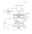
- FIG. 1 is a diagram illustrating a configuration of a lens molding device 100 according to the present embodiment.
- the lens molding device 100 is a device that molds a lens from a resin material, and includes a mold 1, a mold 2, heating devices 3a and 3b, a support device 4, a load cell 5, a pressure control unit 6, a DC power source 7, a switch 8, and an insulating plate. 9a and 9b and a heat insulating plate 9c.
- the mold 1 corresponds to the first mold described in the claims, and is provided on the heating device 3a.
- the mold 2 corresponds to the second mold described in the claims, and is supported above the mold 1 by the support device 4.
- the mold 1 has a transfer surface 1a for transferring a predetermined lens shape to a resin material, and a recess is formed at the center of the transfer surface 1a.
- the mold 2 also has a transfer surface 2a for transferring a predetermined lens shape to the resin material, and a recess is formed at the center of the transfer surface 2a. Further, the transfer surface 2a faces the transfer surface 1a.
- the heating devices 3a and 3b correspond to the curing means described in the claims, and the resin materials supplied onto the transfer surface 1a of the mold 1 are cured by heating the molds 1 and 2, respectively. .
- the start / end of heating may be controlled by a sequence program or the like, or may be controlled manually.
- the load cell 5 is provided between the support device 4 and the mold 2.
- the load cell 5 detects a load applied to itself, converts the load into an electrical signal, and outputs it.
- An electric signal from the load cell 5 is input to the pressure control unit 6.
- the support device 4 includes a support 4a and a drive shaft 4b.
- the support 4a is joined to the load cell 5 and can be expanded and contracted by a drive shaft 4b. Thereby, the support apparatus 4 can move the mold 2 up and down in the drawing.
- the pressure control unit 6 performs expansion / contraction control of the support 4a of the support device 4 based on the electric signal from the load cell 5. As will be described later, the pressure control unit 6 controls the support device 4 so that pressure is applied to the resin material while the resin material supplied between the molds 1 and 2 is cured.
- the pressure control unit 6 may be built in the support device 4. Further, the support device 4 and the pressure control unit 6 constitute pressure applying means described in the claims.
- the DC power source 7 corresponds to the electric field forming means described in the claims.
- the output voltage of the DC power supply 7 is 6 KV, for example, and the DC power supply 7 is connected to the mold 2 via the switch 8.
- the mold 1 is connected to GND.
- an insulating plate 9a is provided between the mold 1 and the heating device 3a, and an insulating plate 9b is provided between the mold 2 and the heating device 3b.
- the heat insulating plate 9 c is disposed between the heating device 3 b and the load cell 5. Thereby, the load cell 5 is not influenced by the heat of the heating device 3b.
- the molds 1 and 2 also function as electrodes for forming an electric field.
- a DC power source 7 may be connected to the mold 1 and the mold 2 may be grounded.
- a DC voltage may be applied between the mold 1 and the mold 2 without grounding the molds 1 and 2.
- the electric field may be formed using an AC power supply instead of the DC power supply 7.
- the resin material 11 is supplied onto the transfer surface 1a of the mold 1 using the dispenser 10 (supply process).
- the resin material 11 corresponds to the dielectric material described in the claims.
- the resin material 11 is a thermosetting resin that is cured by heating, and polarization is generated by applying an electric field. It is a dielectric.
- the support device 4 moves the mold 2 downward and presses the transfer surface 2 a of the mold 2 against the resin material 11.
- the resin material 11 is cured by heating the molds 1 and 2 and the resin material 11 with the heating devices 3a and 3b (curing step).
- the pressure control unit 6 calculates the pressure applied to the resin material 11 in the middle of curing, and controls the support device 4 so that the pressure becomes a predetermined value. . Further, an electric field is formed between the mold 1 and the mold 2 by turning on the switch 8 while the resin material 11 is cured.
- FIG. 5 is a schematic diagram showing a state when the resin material 11 is cured. As shown in the figure, the resin material 11 is deformed so that the portion in contact with the mold 2 is separated from the mold 2 by curing shrinkage. In contrast, a pressure is applied to the resin material 11 during curing, and an electric field is formed between the mold 1 and the mold 2.
- the portion of the resin material 11 facing the mold 2 (upper side) is negatively charged due to dielectric polarization, and the portion of the resin material 11 facing the mold 1 (lower side) is Positively charged.
- the mold 2 is negatively charged and the mold 1 is positively charged. For this reason, as shown by the upward arrow in the figure, an electrostatic attractive force that draws the resin material 11 toward the mold 2 is generated.
- the mold 2 follows the resin material 11 and the contact state between the mold 2 and the resin material 11 is maintained. Therefore, the lens shape error due to the curing shrinkage of the resin material 11 can be greatly reduced.
- the support device 4 raises the mold 2 and separates the transfer surface 2 a from the resin material 11. Thereby, the lens 21 is molded.
- FIG. 7 is a graph showing the relationship between the pressure applied to the resin material, the voltage applied between the molds, and the shape error of the molded product.
- the shape error of the molded product due to the curing shrinkage of the resin material is large.
- the shape error of the object was 0.2186 ⁇ m.
- the shape error of the molded product was 0.1058 ⁇ m.
- the shape error of the molded product is 0 respectively. 0.0465 ⁇ m, 0.0464 ⁇ m, and 0.0239 ⁇ m.
- the transfer accuracy can be improved by about 5 times compared to the case where only the pressure is applied, and further, the transfer accuracy is improved by about 10 times compared to the configuration in which no pressure is applied. I was able to.
- the shape error of the molded product becomes very large in the conventional molding apparatus.
- the shape error of the molded product can be greatly improved.
- FIG. 14 is a diagram showing a configuration of the lens molding apparatus 200 according to the present embodiment.
- the lens molding device 200 is a device that molds a lens from a resin material.
- the members having the same functions as those described in the first embodiment are denoted by the same reference numerals.
- the lens molding process in the present embodiment is substantially the same as that in the first embodiment.
- the present invention can be applied not only to a configuration in which a molded product is molded by two molds, but also to a configuration in which a molded product is molded using one mold and one substrate as in this embodiment. It is.
- the molded product can be molded with high accuracy by the molding apparatus and the molding method according to the present invention.
- the pressure applied to the resin material is 10 N, but the specific value of the pressure is appropriately set depending on the type of the resin material used.
- the curing shrinkage of the resin material is not uniform. Therefore, even if the applied pressure is such that the mold follows the amount of the curing shrinkage, the accuracy of the shape is not significantly improved. Therefore, it is desirable to apply a pressure such that the movement of the mold exceeds the curing shrinkage of the resin material and the mold positively presses the resin material.
- the pressure applied to the resin material may be constant or may change while the resin material is cured.
- the applied pressure may be gradually reduced as the curing of the resin material proceeds.
- the pressure is applied to the resin material via the upper mold, but the direction in which the pressure is applied is not limited to this.
- the configuration shown in FIG. 1 may be a configuration in which pressure is applied to the resin material by pushing up the lower mold 1 without changing the position of the upper mold 2.
- the configuration shown in FIG. 8 the configuration may be such that pressure is applied to the resin material by pushing up the substrate 12 without changing the position of the mold 2.
- thermosetting resin is used as the resin material, but the present invention is not limited to this.
- a photocurable resin that is cured by being irradiated with UV may be used.
- a UV irradiation device is used instead of the heating device.
- the electric field forming means forms the electric field by applying a voltage between the first mold and the second mold. Also good.
- the electric field may be formed by applying a voltage between the first mold and the second mold.
- the electric field forming means may form the electric field by applying a voltage between the mold and the substrate.
- the electric field may be formed by applying a voltage between the substrate and the mold.
- the molded product is preferably a lens.
- the molding apparatus and the molding method according to the embodiment of the present invention are particularly suitable for molding a lens having a complicated shape because a molding can be molded with high accuracy.
- the present invention can be applied not only to a lens molding device and a lens molding method, but also to a molding device and a molding method for molding any molded product other than a lens.
Landscapes
- Engineering & Computer Science (AREA)
- Mechanical Engineering (AREA)
- Health & Medical Sciences (AREA)
- Manufacturing & Machinery (AREA)
- Ophthalmology & Optometry (AREA)
- Casting Or Compression Moulding Of Plastics Or The Like (AREA)
- Moulds For Moulding Plastics Or The Like (AREA)
Abstract
本発明に係るレンズ成形装置(100)は、転写面(1a)を有するモールド(1)と、転写面(2a)を有するモールド(2)と、転写面(1a)上に供給され、転写面(2a)が押し当てられた樹脂材料を加熱して硬化させる加熱装置(3a・3b)と、支持装置(4)が樹脂材料に圧力を印加するように制御する圧力制御部(6)と、モールド(1・2)間に電圧を印加して電界を形成する直流電源(7)とを備える。
Description
本発明は、成形装置および成形方法に関し、特に、レンズ等の複雑な形状を有する成形物を高精度に成形可能な成形装置および成形方法に関する。
従来より、樹脂材料からレンズ等の成形物を成形するために、所定の形状を転写するための転写面を有するモールドの当該転写面を樹脂材料に押し当て、樹脂材料を硬化させることにより、成形物を成形する圧縮成形技術が用いられている。上記樹脂材料としては、例えば、熱可塑性、熱硬化性もしくは光硬化性の材料が用いられ、樹脂材料を加熱するか、あるいは樹脂材料に光を照射することにより、樹脂材料を硬化させる。
このような圧縮成形技術は、例えば特許文献1および2に開示されている。
近年、微細な形状を有する製品には、更なる高精度化が望まれており、例えば、レンズ成形の分野では、光学系の高性能化にともなって、レンズ形状の高精度化がますます重要となっている。しかしながら、上記従来の成形技術では、成形物の形状誤差が大きいため、高精度化が難しいという問題がある。
具体的には、特許文献1および2に開示されている圧縮成形技術では、樹脂材料に転写面を押し当てた後、樹脂材料の硬化が完了するまで、モールドの位置は固定される。しかしながら、樹脂材料は硬化に伴って収縮するため、モールドの転写面が樹脂材料に追従できず、成形物のサイズが転写面によって規定されるサイズよりも小さくなる。そのため、予め樹脂材料の硬化収縮を考慮して、転写面のサイズを成形物のサイズよりも大きくする必要がある。よって、成形物の形状が複雑な場合や、樹脂材料の硬化収縮率が大きい場合は、成形物の形状誤差が大きくなってしまう。
本発明は、上記の問題点を解決するためになされたもので、その目的は、高精度に成形物を成形できる成形装置および成形方法を提供することにある。
上記の課題を解決するために、本発明に係る成形装置は、誘電体材料に所定の形状を転写するための第1の転写面を有する第1のモールドと、前記誘電体材料に所定の形状を転写するための第2の転写面を有し、当該第2の転写面が前記第1の転写面と対向している第2のモールドと、前記第1の転写面上に供給され、前記第2の転写面が押し当てられた前記誘電体材料を硬化させて成形物を成形する硬化手段とを備える成形装置であって、前記硬化手段が前記誘電体材料を硬化させる間に、前記誘電体材料に圧力を印加する圧力印加手段と、前記硬化手段が前記誘電体材料を硬化させる間に、前記第1のモールドと前記第2のモールドとの間に電界を形成する電界形成手段とを備えることを特徴としている。
上記の構成によれば、第1のモールドの第1の転写面上に供給された材料に、第2のモールドの第2の転写面が押し当てられた状態で、硬化手段が前記材料を硬化させることにより、成形物が成形される。ここで、硬化手段が材料を硬化させる間、材料は硬化収縮する。これに対し、材料が硬化されている間に、圧力印加手段によって材料に圧力が印加されるとともに、第1のモールドと第2のモールドとの間に電界が形成されるため、硬化が完了するまで、圧力および電界による静電引力によってモールドが材料に追従して、モールドと材料との接触状態が維持される。そのため、材料の硬化収縮に起因する成形物の形状誤差を大幅に低減することができる。
したがって、高精度に成形物を成形できる成形装置を提供することができる。
上記の課題を解決するために、本発明に係る成形装置は、基板と、誘電体材料に所定の形状を転写するための転写面を有するモールドと、前記基板上に供給され、前記転写面が押し当てられた前記誘電体材料を硬化させて成形物を成形する硬化手段とを備える成形装置であって、前記硬化手段が前記誘電体材料を硬化させる間に、前記誘電体材料に圧力を印加する圧力印加手段と、前記硬化手段が前記誘電体材料を硬化させる間に、前記モールドと前記基板との間に電界を形成する電界形成手段とを備えることを特徴としている。
上記の構成によれば、基板上に供給された材料に、モールドの転写面が押し当てられた状態で、硬化手段が前記材料を硬化させることにより、成形物が成形される。ここで、硬化手段が材料を硬化させる間、材料は硬化収縮する。これに対し、材料が硬化されている間に、圧力印加手段によって材料に圧力が印加されるとともに、モールドと基板との間に電界が形成されるため、硬化が完了するまで、圧力および電界による静電引力によってモールドが材料に追従して、モールドと材料との接触状態が維持される。そのため、材料の硬化収縮に起因する成形物の形状誤差を大幅に低減することができる。
したがって、高精度に成形物を成形できる成形装置を提供することができる。
上記の課題を解決するために、本発明に係る成形方法は、誘電体材料に所定の形状を転写するための第1の転写面を有する第1のモールドの前記第1の転写面上に誘電体材料を供給する供給工程と、誘電体材料に所定の形状を転写するための第2の転写面を有する第2のモールドの前記第2の転写面を、供給された前記誘電体材料に押し当てた状態で、当該誘電体材料を硬化させて成形物を成形する硬化工程とを有する成形方法であって、前記硬化工程の間、前記誘電体材料に圧力を印加するとともに、前記第1のモールドと前記第2のモールドとの間に電界を形成することを特徴としている。
上記の構成によれば、第1のモールドの第1の転写面上に供給された材料に、第2のモールドの第2の転写面が押し当てられた状態で、前記材料を硬化することにより、成形物が成形される。ここで、硬化工程では、材料が硬化収縮する。これに対し、硬化工程の間、材料に圧力が印加されるとともに、第1のモールドと第2のモールドとの間に電界が形成されるため、硬化が完了するまで、圧力および電界による静電引力によってモールドが材料に追従して、モールドと材料との接触状態が維持される。そのため、材料の硬化収縮に起因する成形物の形状誤差を大幅に低減することができる。
したがって、高精度に成形物を成形できる成形方法を提供することができる。
上記の課題を解決するために、本発明に係る成形方法は、基板上に誘電体材料を供給する供給工程と、誘電体材料に所定の形状を転写するための転写面を有するモールドの前記転写面を、供給された前記誘電体材料に押し当てた状態で、当該誘電体材料を硬化させて成形物を成形する硬化工程とを有する成形方法であって、前記硬化工程の間、前記誘電体材料に圧力を印加するとともに、前記基板と前記モールドとの間に電界を形成することを特徴としている。
上記の構成によれば、基板上に供給された材料に、モールドの転写面が押し当てられた状態で、前記材料を硬化することにより、成形物が成形される。ここで、硬化工程では、材料が硬化収縮する。これに対し、硬化工程の間、材料に圧力が印加されるとともに、モールドと基板との間に電界が形成されるため、硬化が完了するまで、圧力および電界による静電引力によってモールドが材料に追従して、モールドと材料との接触状態が維持される。そのため、材料の硬化収縮に起因する成形物の形状誤差を大幅に低減することができる。
したがって、高精度に成形物を成形できる成形方法を提供することができる。
以上のように、本発明に係る成形装置は、誘電体材料に所定の形状を転写するための第1の転写面を有する第1のモールドと、前記誘電体材料に所定の形状を転写するための第2の転写面を有し、当該第2の転写面が前記第1の転写面と対向している第2のモールドと、前記第1の転写面上に供給され、前記第2の転写面が押し当てられた前記誘電体材料を硬化させて成形物を成形する硬化手段とを備える成形装置であって、前記硬化手段が前記誘電体材料を硬化させる間に、前記誘電体材料に圧力を印加する圧力印加手段と、前記硬化手段が前記誘電体材料を硬化させる間に、前記第1のモールドと前記第2のモールドとの間に電界を形成する電界形成手段とを備える構成である。
また、本発明に係る成形方法は、誘電体材料に所定の形状を転写するための第1の転写面を有する第1のモールドの前記第1の転写面上に誘電体材料を供給する供給工程と、誘電体材料に所定の形状を転写するための第2の転写面を有する第2のモールドの前記第2の転写面を、供給された前記誘電体材料に押し当てた状態で、当該誘電体材料を硬化させて成形物を成形する硬化工程とを有する成形方法であって、前記硬化工程の間、前記誘電体材料に圧力を印加するとともに、前記第1のモールドと前記第2のモールドとの間に電界を形成する構成である。
したがって、高精度に成形物を成形できる成形装置および成形方法を提供できるという効果を奏する。
以下では、本発明に係る成形装置の一例として、レンズを成形するレンズ成形装置について説明する。
〔実施形態1〕
本発明の第1の実施形態について図1~図6に基づいて説明すれば、以下のとおりである。
本発明の第1の実施形態について図1~図6に基づいて説明すれば、以下のとおりである。
(レンズ成形装置100の構成)
図1は、本実施形態に係るレンズ成形装置100の構成を示す図である。レンズ成形装置100は、樹脂材料からレンズを成形する装置であり、モールド1、モールド2、加熱装置3a・3b、支持装置4、ロードセル5、圧力制御部6、直流電源7、スイッチ8、絶縁プレート9a・9bおよび断熱プレート9cを備えている。
図1は、本実施形態に係るレンズ成形装置100の構成を示す図である。レンズ成形装置100は、樹脂材料からレンズを成形する装置であり、モールド1、モールド2、加熱装置3a・3b、支持装置4、ロードセル5、圧力制御部6、直流電源7、スイッチ8、絶縁プレート9a・9bおよび断熱プレート9cを備えている。
モールド1は、特許請求の範囲に記載の第1のモールドに相当するものであり、加熱装置3a上に設けられている。また、モールド2は、特許請求の範囲に記載の第2のモールドに相当するものであり、支持装置4によってモールド1の上方に支持されている。
モールド1は、樹脂材料に所定のレンズ形状を転写するための転写面1aを有しており、転写面1aの中心部には、凹部が形成されている。同様に、モールド2も、樹脂材料に所定のレンズ形状を転写するための転写面2aを有しており、転写面2aの中心部には、凹部が形成されている。また、転写面2aは転写面1aと対向している。
加熱装置3a・3bは、特許請求の範囲に記載の硬化手段に相当するものであり、それぞれモールド1・2を加熱することにより、モールド1の転写面1a上に供給された樹脂材料を硬化させる。加熱の開始/終了は、シーケンスプログラム等によって制御してもよいし、手動で制御してもよい。
ロードセル5は、支持装置4とモールド2との間に設けられている。ロードセル5は、自身にかかる荷重を検知して、当該荷重を電気信号に変換して出力する。ロードセル5からの電気信号は、圧力制御部6に入力される。
支持装置4は、支持体4aおよび駆動軸4bを備えている。支持体4aはロードセル5に接合されており、駆動軸4bによって伸縮可能となっている。これにより、支持装置4は、モールド2を図中上下に移動させることができる。
圧力制御部6は、ロードセル5からの電気信号に基づいて支持装置4の支持体4aの伸縮制御を行うものである。後述するように、圧力制御部6は、モールド1・2間に供給された樹脂材料が硬化される間に、当該樹脂材料に圧力が印加されるように、支持装置4を制御する。
なお、圧力制御部6は、支持装置4に内蔵されていてもよい。また、支持装置4および圧力制御部6は、特許請求の範囲に記載の圧力印加手段を構成している。
直流電源7は、特許請求の範囲に記載の電界形成手段に相当するものである。直流電源7の出力電圧は、例えば6KVであり、直流電源7は、スイッチ8を介してモールド2に接続されている。一方、モールド1はGNDに接続されている。さらに、モールド1と加熱装置3aとの間に、絶縁プレート9aが設けられ、モールド2と加熱装置3bとの間に、絶縁プレート9bが設けられている。
断熱プレート9cは、加熱装置3bとロードセル5との間に配置されている。これにより、ロードセル5は、加熱装置3bの熱による影響を受けることがない。
上記の構成により、スイッチ8をONさせると、モールド1とモールド2との間に電界を形成することができる。すなわち、モールド1・2は、電界を形成するための電極としても機能する。
なお、電界を形成するために、モールド1に直流電源7を接続し、モールド2を接地してもよい。あるいは、モールド1・2を接地せずに、モールド1とモールド2との間に直流電圧をかけてもよい。あるいは、直流電源7の代わりに交流電源を用いて電界を形成してもよい。
(レンズの成形工程)
続いて、レンズ成形装置100におけるレンズの成形工程について、図2~図6を参照して説明する。
続いて、レンズ成形装置100におけるレンズの成形工程について、図2~図6を参照して説明する。
まず、図2に示すように、ディスペンサ10を用いて、モールド1の転写面1a上に樹脂材料11を供給する(供給工程)。樹脂材料11は、特許請求の範囲に記載の誘電体材料に相当するものであり、本実施形態では、加熱されることにより硬化する熱硬化性樹脂であるとともに、電界を与えることにより分極が生じる誘電体である。
続いて、図3に示すように、支持装置4がモールド2を下方に移動させて、モールド2の転写面2aを樹脂材料11に押し当てる。この状態で、加熱装置3a・3bによりモールド1・2および樹脂材料11を加熱することにより、樹脂材料11を硬化させる(硬化工程)。
樹脂材料11が硬化している間、図4に示すように、樹脂材料11に圧力が印加される。具体的には、ロードセル5が検知する荷重に基づいて、圧力制御部6が、硬化途中の樹脂材料11にかかる圧力を算出し、当該圧力が所定の値になるように支持装置4を制御する。さらに、樹脂材料11が硬化している間、スイッチ8がONすることにより、モールド1とモールド2との間に電界が形成される。
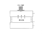
図5は、樹脂材料11の硬化時の状態を示す模式図である。同図に示すように、硬化収縮により、樹脂材料11は、モールド2と接触している部分がモールド2から離間するように変形する。これに対し、硬化時に樹脂材料11に圧力が印加されるとともに、モールド1とモールド2との間に電界が形成される。
樹脂材料11は絶縁体であるため、誘電分極によって、樹脂材料11のモールド2と対向する部分(上側)は、負に帯電し、樹脂材料11のモールド1と対向する部分(下側)は、正に帯電する。一方、モールド2は負に帯電し、モールド1は正に帯電する。このため、図中上向きの矢印に示すように、樹脂材料11をモールド2に引き寄せる静電引力が発生する。
よって、硬化が完了するまで、モールド2が樹脂材料11に追従して、モールド2と樹脂材料11との接触状態が維持される。したがって、樹脂材料11の硬化収縮に起因するレンズ形状の誤差を大幅に低減することができる。
硬化が完了すると、図6に示すように、支持装置4がモールド2を上昇させ、転写面2aを樹脂材料11から引き離す。これにより、レンズ21が成形される。
(効果の検証)
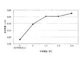
図7は、樹脂材料に印加する圧力およびモールド間に印加する電圧と、成形物の形状誤差との関係を示すグラフである。
図7は、樹脂材料に印加する圧力およびモールド間に印加する電圧と、成形物の形状誤差との関係を示すグラフである。
従来の成形装置では、樹脂材料を硬化させる間、2つのモールドの位置が固定されるので、樹脂材料の硬化収縮による成形物の形状誤差が大きく、発明者による実験では、従来の成形装置における成形物の形状誤差は、0.2186μmであった。一方、樹脂材料の硬化時に10Nの圧力を印加した場合、成形物の形状誤差は0.1058μmであった。さらに、本実施形態のように、樹脂材料の硬化時に10Nの圧力を印加するとともに、1.5KV、4.5KV、6.0KVの電圧を印加した場合における成形物の形状誤差は、それぞれ、0.0465μm、0.0464μm、0.0239μmであった。特に、印加電圧が6.0KVの場合では、圧力のみ印加する場合に比べ、転写精度を約5倍向上させることができ、さらに、圧力を印加しない構成に比べ、転写精度を約10倍向上させることができた。
このように、硬化途中の樹脂材料へ圧力を印加するとともに、2つのモールド間に電界を形成することにより、成形物の形状誤差をさらに低減することができた。
特に、硬化収縮率が大きい樹脂材料を用いる場合、従来の成形装置では成形物の形状誤差が非常に大きくなる。これに対し、本実施形態では、モールドが樹脂材料に追従するので、成形物の形状誤差を大幅に改善することができる。
〔実施形態2〕
本発明の第2の実施形態について図8に基づいて説明すれば、以下のとおりである。
本発明の第2の実施形態について図8に基づいて説明すれば、以下のとおりである。
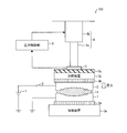
図14は、本実施形態に係るレンズ成形装置200の構成を示す図である。レンズ成形装置200は、樹脂材料からレンズを成形する装置であり、モールド2、加熱装置3a・3b、支持装置4、ロードセル5、圧力制御部6、直流電源7、スイッチ8および絶縁プレート9a・9b、断熱プレート9cおよび基板12を備えている。すなわち、レンズ成形装置200は、前記の実施形態1に係るレンズ成形装置100において、モールド1を基板12に置き換えた構成である。
前記の実施形態1において説明した部材と同じ機能を有する部材については、同じ符号を付記している。また、本実施形態における、レンズの成形工程は、前記の実施形態1におけるものと略同一である。
このように、本発明は、2つのモールドによって成形物を成形する構成だけでなく、本実施形態のように、1つのモールドと1つの基板とを用いて成形物を成形する構成にも適用可能である。
〔実施形態の総括〕
以上のように、本発明に係る成形装置および成形方法によって、成形物を高精度に成形することができる。
以上のように、本発明に係る成形装置および成形方法によって、成形物を高精度に成形することができる。
また、検証実験では、樹脂材料に印加する圧力を10Nとしたが、圧力の具体的な数値は、用いられる樹脂材料の種類などによって適宜設定される。なお、成形物の形状が複雑な場合、樹脂材料の硬化収縮は均等ではないため、印加される圧力が、モールドを硬化収縮分だけ追従させる程度であっても、形状の精度はあまり向上しない。そのため、モールドの移動が樹脂材料の硬化収縮を上回り、モールドが樹脂材料を積極的に押圧する程度の圧力を印加することが望ましい。
また、樹脂材料に印加する圧力は、樹脂材料が硬化する間、一定であってもよいし、変化してもよい。例えば、樹脂材料の硬化の進行に従って、印加する圧力を徐々に低下させてもよい。
また、上述した各実施形態では、上側のモールドを介して樹脂材料に圧力を印加する構成であったが、圧力を印加する方向はこれに限定されない。例えば、図1に示す構成において、上側のモールド2の位置を変化させずに、下側のモールド1を押し上げることにより、樹脂材料に圧力を印加する構成であってもよい。同様に、図8に示す構成において、モールド2の位置を変化させずに、基板12を押し上げることにより、樹脂材料に圧力を印加する構成であってもよい。
また、上述した各実施形態では、樹脂材料として熱硬化性樹脂を用いたが、これに限定されない。例えば、UVを照射されることにより硬化する光硬化性樹脂を用いてもよい。この場合、加熱装置の代わりに、UV照射装置が用いられる。
本発明は上述した各実施形態に限定されるものではなく、請求項に示した範囲で種々の変更が可能であり、異なる実施形態にそれぞれ開示された技術的手段を適宜組み合わせて得られる実施形態についても本発明の技術的範囲に含まれる。
(要点概要)
以上のように、本発明の実施形態に係る成形装置では、前記電界形成手段は、前記第1のモールドと前記第2のモールドとの間に電圧を印加することにより、前記電界を形成してもよい。
以上のように、本発明の実施形態に係る成形装置では、前記電界形成手段は、前記第1のモールドと前記第2のモールドとの間に電圧を印加することにより、前記電界を形成してもよい。
本発明の実施形態に係る成形方法では、前記第1のモールドと前記第2のモールドとの間に電圧を印加することにより、前記電界を形成してもよい。
本発明の実施形態に係る成形装置では、前記電界形成手段は、前記モールドと前記基板との間に電圧を印加することにより、前記電界を形成してもよい。
本発明の実施形態に係る成形方法では、前記基板と前記モールドとの間に電圧を印加することにより、前記電界を形成してもよい。
本発明の実施形態に係る成形装置および成形方法では、前記成形物はレンズであることが好ましい。
上記のように、本発明の実施形態に係る成形装置および成形方法は、高精度に成形物を成形することができるので、複雑な形状を有するレンズの成形に特に好適である。
本発明は、レンズ成形装置およびレンズ成形方法だけでなく、レンズ以外のあらゆる成形物を成形するための成形装置および成形方法に適用することができる。
1 モールド(第1のモールド)
1a 転写面(第1の転写面)
2 モールド(第2のモールド)
2a 転写面(第2の転写面)
3a 加熱装置(硬化手段)
3b 加熱装置(硬化手段)
4 支持装置(圧力印加手段)
4a 支持体
4b 駆動軸
5 ロードセル
6 圧力制御部(圧力印加手段)
7 直流電源(電界形成手段)
8 スイッチ
9a 絶縁プレート
9b 絶縁プレート
9c 断熱プレート
10 ディスペンサ
11 樹脂材料(誘電体材料)
12 基板
21 レンズ(成形物)
100 レンズ成形装置(成形装置)
200 レンズ成形装置(成形装置)
1a 転写面(第1の転写面)
2 モールド(第2のモールド)
2a 転写面(第2の転写面)
3a 加熱装置(硬化手段)
3b 加熱装置(硬化手段)
4 支持装置(圧力印加手段)
4a 支持体
4b 駆動軸
5 ロードセル
6 圧力制御部(圧力印加手段)
7 直流電源(電界形成手段)
8 スイッチ
9a 絶縁プレート
9b 絶縁プレート
9c 断熱プレート
10 ディスペンサ
11 樹脂材料(誘電体材料)
12 基板
21 レンズ(成形物)
100 レンズ成形装置(成形装置)
200 レンズ成形装置(成形装置)
Claims (10)
- 誘電体材料に所定の形状を転写するための第1の転写面を有する第1のモールドと、
前記誘電体材料に所定の形状を転写するための第2の転写面を有し、当該第2の転写面が前記第1の転写面と対向している第2のモールドと、
前記第1の転写面上に供給され、前記第2の転写面が押し当てられた前記誘電体材料を硬化させて成形物を成形する硬化手段とを備える成形装置であって、
前記硬化手段が前記誘電体材料を硬化させる間に、前記誘電体材料に圧力を印加する圧力印加手段と、
前記硬化手段が前記誘電体材料を硬化させる間に、前記第1のモールドと前記第2のモールドとの間に電界を形成する電界形成手段とを備えることを特徴とする成形装置。 - 基板と、
誘電体材料に所定の形状を転写するための転写面を有するモールドと、
前記基板上に供給され、前記転写面が押し当てられた前記誘電体材料を硬化させて成形物を成形する硬化手段とを備える成形装置であって、
前記硬化手段が前記誘電体材料を硬化させる間に、前記誘電体材料に圧力を印加する圧力印加手段と、
前記硬化手段が前記誘電体材料を硬化させる間に、前記モールドと前記基板との間に電界を形成する電界形成手段とを備えることを特徴とする成形装置。 - 前記電界形成手段は、前記第1のモールドと前記第2のモールドとの間に電圧を印加することにより、前記電界を形成することを特徴とする請求項1に記載の成形装置。
- 前記電界形成手段は、前記モールドと前記基板との間に電圧を印加することにより、前記電界を形成することを特徴とする請求項2に記載の成形装置。
- 前記成形物はレンズであることを特徴とする請求項1~4のいずれか1項に記載の成形装置。
- 誘電体材料に所定の形状を転写するための第1の転写面を有する第1のモールドの前記第1の転写面上に誘電体材料を供給する供給工程と、
誘電体材料に所定の形状を転写するための第2の転写面を有する第2のモールドの前記第2の転写面を、供給された前記誘電体材料に押し当てた状態で、当該誘電体材料を硬化させて成形物を成形する硬化工程とを有する成形方法であって、
前記硬化工程の間、前記誘電体材料に圧力を印加するとともに、前記第1のモールドと前記第2のモールドとの間に電界を形成することを特徴とする成形方法。 - 基板上に誘電体材料を供給する供給工程と、
誘電体材料に所定の形状を転写するための転写面を有するモールドの前記転写面を、供給された前記誘電体材料に押し当てた状態で、当該誘電体材料を硬化させて成形物を成形する硬化工程とを有する成形方法であって、
前記硬化工程の間、前記誘電体材料に圧力を印加するとともに、前記基板と前記モールドとの間に電界を形成することを特徴とする成形方法。 - 前記第1のモールドと前記第2のモールドとの間に電圧を印加することにより、前記電界を形成することを特徴とする請求項6に記載の成形方法。
- 前記基板と前記モールドとの間に電圧を印加することにより、前記電界を形成することを特徴とする請求項7に記載の成形方法。
- 前記成形物はレンズであることを特徴とする請求項6~9のいずれか1項に記載の成形方法。
Priority Applications (2)
| Application Number | Priority Date | Filing Date | Title |
|---|---|---|---|
| CN201280046402.4A CN103813894A (zh) | 2011-09-29 | 2012-07-23 | 成型装置以及成型方法 |
| US14/345,853 US10286615B2 (en) | 2011-09-29 | 2012-07-23 | Molding apparatus and molding method |
Applications Claiming Priority (2)
| Application Number | Priority Date | Filing Date | Title |
|---|---|---|---|
| JP2011-215474 | 2011-09-29 | ||
| JP2011215474A JP5203493B2 (ja) | 2011-09-29 | 2011-09-29 | 成形装置および成形方法 |
Publications (1)
| Publication Number | Publication Date |
|---|---|
| WO2013046887A1 true WO2013046887A1 (ja) | 2013-04-04 |
Family
ID=47994942
Family Applications (1)
| Application Number | Title | Priority Date | Filing Date |
|---|---|---|---|
| PCT/JP2012/068633 Ceased WO2013046887A1 (ja) | 2011-09-29 | 2012-07-23 | 成形装置および成形方法 |
Country Status (5)
| Country | Link |
|---|---|
| US (1) | US10286615B2 (ja) |
| JP (1) | JP5203493B2 (ja) |
| CN (1) | CN103813894A (ja) |
| TW (1) | TWI469859B (ja) |
| WO (1) | WO2013046887A1 (ja) |
Families Citing this family (6)
| Publication number | Priority date | Publication date | Assignee | Title |
|---|---|---|---|---|
| US9868710B2 (en) | 2013-10-31 | 2018-01-16 | Zeon Corporation | Polymerizable compound, polymerizable composition, polymer, and optically anisotropic product |
| CN104786418B (zh) * | 2015-04-29 | 2017-07-25 | 常渭锋 | 一种真空高温热压成型机 |
| CA3054965A1 (en) | 2017-03-16 | 2018-09-20 | Molecular Imprints, Inc. | Optical polymer films and methods for casting the same |
| EP4420867B1 (en) | 2017-10-17 | 2026-02-18 | Magic Leap, Inc. | Method of forming a waveguide |
| CN117141017B (zh) | 2018-10-16 | 2024-08-30 | 奇跃公司 | 用于浇铸聚合物产品的方法和装置 |
| TWI776003B (zh) * | 2018-12-14 | 2022-09-01 | 揚明光學股份有限公司 | 模造鏡片的製造設備及方法 |
Citations (3)
| Publication number | Priority date | Publication date | Assignee | Title |
|---|---|---|---|---|
| JP2005527974A (ja) * | 2002-05-24 | 2005-09-15 | ワイ. チョウ,スティーヴン, | 界誘導圧力インプリント・リソグラフィの方法および装置 |
| WO2010119726A1 (ja) * | 2009-04-13 | 2010-10-21 | コニカミノルタオプト株式会社 | ウエハレンズの製造方法 |
| JP2011073300A (ja) * | 2009-09-30 | 2011-04-14 | Sharp Corp | レンズ成形装置およびレンズ成形方法 |
Family Cites Families (25)
| Publication number | Priority date | Publication date | Assignee | Title |
|---|---|---|---|---|
| EP0416791A2 (en) | 1989-09-08 | 1991-03-13 | General Motors Corporation | Method and apparatus for compression moulding with dielectric heating |
| US6518189B1 (en) | 1995-11-15 | 2003-02-11 | Regents Of The University Of Minnesota | Method and apparatus for high density nanostructures |
| US20040137734A1 (en) | 1995-11-15 | 2004-07-15 | Princeton University | Compositions and processes for nanoimprinting |
| US8603386B2 (en) | 1995-11-15 | 2013-12-10 | Stephen Y. Chou | Compositions and processes for nanoimprinting |
| US20040036201A1 (en) | 2000-07-18 | 2004-02-26 | Princeton University | Methods and apparatus of field-induced pressure imprint lithography |
| US8728380B2 (en) | 1995-11-15 | 2014-05-20 | Regents Of The University Of Minnesota | Lithographic method for forming a pattern |
| US5772905A (en) | 1995-11-15 | 1998-06-30 | Regents Of The University Of Minnesota | Nanoimprint lithography |
| US6309580B1 (en) | 1995-11-15 | 2001-10-30 | Regents Of The University Of Minnesota | Release surfaces, particularly for use in nanoimprint lithography |
| US20080217813A1 (en) | 1995-11-15 | 2008-09-11 | Chou Stephen Y | Release surfaces, particularly for use in nanoimprint lithography |
| US6482742B1 (en) | 2000-07-18 | 2002-11-19 | Stephen Y. Chou | Fluid pressure imprint lithography |
| US8128856B2 (en) | 1995-11-15 | 2012-03-06 | Regents Of The University Of Minnesota | Release surfaces, particularly for use in nanoimprint lithography |
| JPH10180786A (ja) | 1996-12-26 | 1998-07-07 | Komatsu Ltd | プラスチックの圧縮成形方法および圧縮成形金型 |
| US8852494B2 (en) | 1999-10-08 | 2014-10-07 | Princeton University | Method and apparatus of electrical field assisted imprinting |
| US7322287B2 (en) | 2000-07-18 | 2008-01-29 | Nanonex Corporation | Apparatus for fluid pressure imprint lithography |
| US7635262B2 (en) | 2000-07-18 | 2009-12-22 | Princeton University | Lithographic apparatus for fluid pressure imprint lithography |
| US20100236705A1 (en) | 2000-07-18 | 2010-09-23 | Chou Stephen Y | Fluidic and Microdevice Apparatus and Methods For Bonding Components Thereof |
| US20050037143A1 (en) | 2000-07-18 | 2005-02-17 | Chou Stephen Y. | Imprint lithography with improved monitoring and control and apparatus therefor |
| US7211214B2 (en) | 2000-07-18 | 2007-05-01 | Princeton University | Laser assisted direct imprint lithography |
| US7717696B2 (en) | 2000-07-18 | 2010-05-18 | Nanonex Corp. | Apparatus for double-sided imprint lithography |
| US20080213418A1 (en) | 2000-07-18 | 2008-09-04 | Hua Tan | Align-transfer-imprint system for imprint lithogrphy |
| US20040120644A1 (en) | 2000-07-18 | 2004-06-24 | Chou Stephen Y | Method of making subwavelength resonant grating filter |
| US6964793B2 (en) | 2002-05-16 | 2005-11-15 | Board Of Regents, The University Of Texas System | Method for fabricating nanoscale patterns in light curable compositions using an electric field |
| US7510946B2 (en) | 2003-03-17 | 2009-03-31 | Princeton University | Method for filling of nanoscale holes and trenches and for planarizing of a wafer surface |
| JP2006064950A (ja) * | 2004-08-26 | 2006-03-09 | Fuji Photo Film Co Ltd | レンズアレイ製造方法、およびレンズアレイ製造装置 |
| EP2008786A4 (en) * | 2006-04-20 | 2010-03-17 | Sumitomo Heavy Industries | RESIN FORMAT AND RESIN FORMING METHOD |
-
2011
- 2011-09-29 JP JP2011215474A patent/JP5203493B2/ja active Active
-
2012
- 2012-07-23 WO PCT/JP2012/068633 patent/WO2013046887A1/ja not_active Ceased
- 2012-07-23 US US14/345,853 patent/US10286615B2/en active Active
- 2012-07-23 CN CN201280046402.4A patent/CN103813894A/zh active Pending
- 2012-08-03 TW TW101128141A patent/TWI469859B/zh active
Patent Citations (3)
| Publication number | Priority date | Publication date | Assignee | Title |
|---|---|---|---|---|
| JP2005527974A (ja) * | 2002-05-24 | 2005-09-15 | ワイ. チョウ,スティーヴン, | 界誘導圧力インプリント・リソグラフィの方法および装置 |
| WO2010119726A1 (ja) * | 2009-04-13 | 2010-10-21 | コニカミノルタオプト株式会社 | ウエハレンズの製造方法 |
| JP2011073300A (ja) * | 2009-09-30 | 2011-04-14 | Sharp Corp | レンズ成形装置およびレンズ成形方法 |
Also Published As
| Publication number | Publication date |
|---|---|
| US20140217626A1 (en) | 2014-08-07 |
| CN103813894A (zh) | 2014-05-21 |
| JP2013075379A (ja) | 2013-04-25 |
| TWI469859B (zh) | 2015-01-21 |
| JP5203493B2 (ja) | 2013-06-05 |
| US10286615B2 (en) | 2019-05-14 |
| TW201313434A (zh) | 2013-04-01 |
Similar Documents
| Publication | Publication Date | Title |
|---|---|---|
| JP5203493B2 (ja) | 成形装置および成形方法 | |
| CN111225780B (zh) | 用于铸造聚合物产品的方法和装置 | |
| EP1509379B1 (en) | Methods and apparatus of field-induced pressure imprint lithography | |
| JP5893303B2 (ja) | インプリント装置、それを用いた物品の製造方法 | |
| JP4806063B2 (ja) | レンズ成形装置およびレンズ成形方法 | |
| KR101714737B1 (ko) | 범프형 스탬프를 이용한 선택적 전사방법 및 전사장치 | |
| JP2018514426A (ja) | 積層造形装置 | |
| KR102602905B1 (ko) | 성형 장치 및 물품 제조 방법 | |
| JP5154675B2 (ja) | 樹脂成形装置および樹脂成形方法 | |
| KR20160056278A (ko) | 임프린트 방법, 임프린트 장치, 몰드 및, 물품 제조 방법 | |
| JPWO2012029843A1 (ja) | 転写システムおよび転写方法 | |
| CN103159164A (zh) | 一种高深宽比微柱阵列的电场诱导压印方法 | |
| JP2018082127A5 (ja) | ||
| US11472097B2 (en) | Imprint apparatus, imprint method, and article manufacturing method | |
| TW201038394A (en) | Patterning method, patterning apparatus, and method for manufacturing semiconductor device | |
| JP6651716B2 (ja) | モールド成形品の製造方法及びモールド成形品の製造装置 | |
| WO2010035540A1 (ja) | ウエハレンズの製造装置及び製造方法 | |
| KR101208898B1 (ko) | 시트 제조 장치 | |
| WO2021200562A1 (ja) | 電子部品の製造方法 | |
| KR20170067665A (ko) | 임프린트 장치 및 방법 | |
| KR20110092546A (ko) | 나노 임프린트용 장치 및 이를 이용한 반도체 소자의 형성방법 | |
| KR20180055709A (ko) | 임프린트 장치, 및 물품 제조 방법 | |
| KR20220146029A (ko) | 렌즈 이형성이 향상된 웨이퍼 렌즈 제조 장치 및 그 방법 | |
| JP2022147478A (ja) | プラスチック素子の製造方法、及びプラスチック素子の製造装置 | |
| JP2005111762A (ja) | 電気泳動表示装置用セル基板の製造方法 |
Legal Events
| Date | Code | Title | Description |
|---|---|---|---|
| 121 | Ep: the epo has been informed by wipo that ep was designated in this application |
Ref document number: 12835305 Country of ref document: EP Kind code of ref document: A1 |
|
| WWE | Wipo information: entry into national phase |
Ref document number: 14345853 Country of ref document: US |
|
| NENP | Non-entry into the national phase |
Ref country code: DE |
|
| 122 | Ep: pct application non-entry in european phase |
Ref document number: 12835305 Country of ref document: EP Kind code of ref document: A1 |