WO2013031867A1 - 表示装置及びその駆動方法 - Google Patents
表示装置及びその駆動方法 Download PDFInfo
- Publication number
- WO2013031867A1 WO2013031867A1 PCT/JP2012/071912 JP2012071912W WO2013031867A1 WO 2013031867 A1 WO2013031867 A1 WO 2013031867A1 JP 2012071912 W JP2012071912 W JP 2012071912W WO 2013031867 A1 WO2013031867 A1 WO 2013031867A1
- Authority
- WO
- WIPO (PCT)
- Prior art keywords
- image
- gradation
- input image
- display
- input
- Prior art date
- Legal status (The legal status is an assumption and is not a legal conclusion. Google has not performed a legal analysis and makes no representation as to the accuracy of the status listed.)
- Ceased
Links
Images








Classifications
-
- G—PHYSICS
- G09—EDUCATION; CRYPTOGRAPHY; DISPLAY; ADVERTISING; SEALS
- G09G—ARRANGEMENTS OR CIRCUITS FOR CONTROL OF INDICATING DEVICES USING STATIC MEANS TO PRESENT VARIABLE INFORMATION
- G09G3/00—Control arrangements or circuits, of interest only in connection with visual indicators other than cathode-ray tubes
- G09G3/20—Control arrangements or circuits, of interest only in connection with visual indicators other than cathode-ray tubes for presentation of an assembly of a number of characters, e.g. a page, by composing the assembly by combination of individual elements arranged in a matrix no fixed position being assigned to or needed to be assigned to the individual characters or partial characters
- G09G3/34—Control arrangements or circuits, of interest only in connection with visual indicators other than cathode-ray tubes for presentation of an assembly of a number of characters, e.g. a page, by composing the assembly by combination of individual elements arranged in a matrix no fixed position being assigned to or needed to be assigned to the individual characters or partial characters by control of light from an independent source
- G09G3/36—Control arrangements or circuits, of interest only in connection with visual indicators other than cathode-ray tubes for presentation of an assembly of a number of characters, e.g. a page, by composing the assembly by combination of individual elements arranged in a matrix no fixed position being assigned to or needed to be assigned to the individual characters or partial characters by control of light from an independent source using liquid crystals
- G09G3/3607—Control arrangements or circuits, of interest only in connection with visual indicators other than cathode-ray tubes for presentation of an assembly of a number of characters, e.g. a page, by composing the assembly by combination of individual elements arranged in a matrix no fixed position being assigned to or needed to be assigned to the individual characters or partial characters by control of light from an independent source using liquid crystals for displaying colours or for displaying grey scales with a specific pixel layout, e.g. using sub-pixels
-
- G—PHYSICS
- G09—EDUCATION; CRYPTOGRAPHY; DISPLAY; ADVERTISING; SEALS
- G09G—ARRANGEMENTS OR CIRCUITS FOR CONTROL OF INDICATING DEVICES USING STATIC MEANS TO PRESENT VARIABLE INFORMATION
- G09G3/00—Control arrangements or circuits, of interest only in connection with visual indicators other than cathode-ray tubes
- G09G3/20—Control arrangements or circuits, of interest only in connection with visual indicators other than cathode-ray tubes for presentation of an assembly of a number of characters, e.g. a page, by composing the assembly by combination of individual elements arranged in a matrix no fixed position being assigned to or needed to be assigned to the individual characters or partial characters
- G09G3/2007—Display of intermediate tones
- G09G3/2044—Display of intermediate tones using dithering
- G09G3/2051—Display of intermediate tones using dithering with use of a spatial dither pattern
-
- G—PHYSICS
- G09—EDUCATION; CRYPTOGRAPHY; DISPLAY; ADVERTISING; SEALS
- G09G—ARRANGEMENTS OR CIRCUITS FOR CONTROL OF INDICATING DEVICES USING STATIC MEANS TO PRESENT VARIABLE INFORMATION
- G09G2320/00—Control of display operating conditions
- G09G2320/02—Improving the quality of display appearance
- G09G2320/0233—Improving the luminance or brightness uniformity across the screen
-
- G—PHYSICS
- G09—EDUCATION; CRYPTOGRAPHY; DISPLAY; ADVERTISING; SEALS
- G09G—ARRANGEMENTS OR CIRCUITS FOR CONTROL OF INDICATING DEVICES USING STATIC MEANS TO PRESENT VARIABLE INFORMATION
- G09G3/00—Control arrangements or circuits, of interest only in connection with visual indicators other than cathode-ray tubes
- G09G3/20—Control arrangements or circuits, of interest only in connection with visual indicators other than cathode-ray tubes for presentation of an assembly of a number of characters, e.g. a page, by composing the assembly by combination of individual elements arranged in a matrix no fixed position being assigned to or needed to be assigned to the individual characters or partial characters
- G09G3/34—Control arrangements or circuits, of interest only in connection with visual indicators other than cathode-ray tubes for presentation of an assembly of a number of characters, e.g. a page, by composing the assembly by combination of individual elements arranged in a matrix no fixed position being assigned to or needed to be assigned to the individual characters or partial characters by control of light from an independent source
- G09G3/36—Control arrangements or circuits, of interest only in connection with visual indicators other than cathode-ray tubes for presentation of an assembly of a number of characters, e.g. a page, by composing the assembly by combination of individual elements arranged in a matrix no fixed position being assigned to or needed to be assigned to the individual characters or partial characters by control of light from an independent source using liquid crystals
- G09G3/3611—Control of matrices with row and column drivers
- G09G3/3648—Control of matrices with row and column drivers using an active matrix
- G09G3/3666—Control of matrices with row and column drivers using an active matrix with the matrix divided into sections
Definitions
- the present invention relates to a display device such as a liquid crystal display device and a driving method thereof.
- the color filter is divided into two on the left and right due to its structure.
- a boundary luminance difference
- a boundary is visually recognized in a region corresponding to a joint portion between the two color filters on the display screen of the display panel.
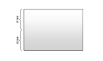
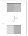
- FIG. 28 is a figure which shows a display state when a luminance difference exists in the display screen of a display panel.
- a left color filter is disposed in the left region
- a right color filter is disposed in the right region.
- a boundary is visually recognized in the central portion corresponding to the joint portion of the left and right color filters.
- a display device that performs gradation correction has been proposed as a technique for reducing the display unevenness (luminance difference). Specifically, when there is a luminance difference between the left and right sides of the display screen, gradation correction is performed so that one luminance matches the other luminance. For example, as shown in FIG. 28A, when the luminance of the left region of the display screen is lower (darker) than the luminance of the right region, the luminance of the left region is increased (brighter). The gradation value of the data signal (input image) corresponding to the left area is increased. As a result, as shown in FIG. 28B, the display luminance is made uniform on the left and right, and display unevenness can be reduced.
- the size and position of a rectangular area on the display screen are designated, the range is gradation-corrected, and the gradation change in the peripheral portion is gradually reduced in the vertical and horizontal directions. By doing so, display unevenness is reduced.
- JP 2005-134560 A (published May 26, 2005)”
- 29A schematically shows a case where the difference in luminance between the left and right sides of the display screen is smaller than 0.5 gradation, and the left area of the display screen is slightly smaller than the right area. It is dark.
- conventional gradation correction for example, correction for raising only the left area by one gradation is performed (the right area is not corrected)
- the left and right contrasts are reversed, as shown in FIG.
- the left area of the display screen is brighter than the right area.
- the difference between the left and right luminances on the display screen after correction (FIG. 29B) is larger than the difference between the left and right luminances on the display screen before correction (FIG. 29A), and before the correction.
- the display quality will deteriorate.
- the present invention is to provide a display device that can reliably reduce display unevenness and improve display quality, and a driving method thereof.
- a display device provides A display device that displays an input image corresponding to the input image data on a display screen based on the input image data, When an image having the same gradation is displayed in at least a partial area of the display screen, a pattern image preset according to the input image is displayed in at least a predetermined area within the area.
- a pattern image set in advance at the luminance boundary portion can be displayed.
- the pattern image can be, for example, a checkered pattern composed of two gradations corresponding to the display luminance.
- the above correction processing for reducing display unevenness is effective even for a minute luminance difference (for example, a luminance difference of one gradation or less). Therefore, display unevenness can be reliably reduced and display quality can be improved.
- a display device driving method for displaying an input image corresponding to the input image data on a display screen based on input image data, An image acquisition process for receiving the input image from the outside; A determination step of recognizing the received input image and determining whether or not the input image needs to be corrected; A correction image acquisition step for acquiring a pattern image stored in advance in the storage unit corresponding to the recognized input image when it is determined that correction is required in the determination step; A correction image generation step of generating a correction image based on the pattern image acquired in the correction image acquisition step and the input image received in the image acquisition step; When it is determined that correction is necessary in the determination step, display is performed based on the corrected image.
- the display device and the driving method thereof when an image having the same gradation is displayed in at least a partial area of the display screen, the input image is displayed in at least a predetermined area in the area. In response to this, a preset pattern image is displayed. Accordingly, it is possible to provide a display device and a driving method thereof that can reliably reduce display unevenness and improve display quality.
- FIG. 6 is a diagram illustrating a display state of a display screen using a corrected image according to Embodiment 1.
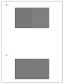
- FIG. It is a figure which shows the image corresponded to A gradation input from the external signal source. It is a figure which shows the display state of the display screen when not performing the correction process which concerns on this Embodiment.
- A is a figure which shows an image when the brightness
- FIG. 9 is a diagram showing a display state of a display screen when a pattern image is displayed in the image shown in FIG. 8.
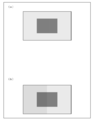
- A) is an image to be displayed, and shows a low gradation image as a whole, in which the luminance (gradation) of the central area of the display screen is different from the luminance (gradation) of the surrounding area.
- FIG. 10 is a diagram illustrating a display state of a display screen using a corrected image according to the second embodiment.
- (A)-(d) is a figure which shows the pattern image according to a gradation level.
- FIG. 10 is a diagram illustrating a display state of a display screen using a corrected image according to the third embodiment.
- FIG. 10 is a diagram illustrating a display state of a display screen using a corrected image according to a fourth embodiment.
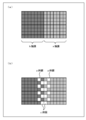
- FIG. 1 shows the display state of a display screen when the gradation of an input image (solid image) is made into a gradation
- (a) shows the display state when not performing a correction process,
- the right side of a display screen is The left side is represented by the luminance corresponding to the b gradation, and the left side is represented by the luminance corresponding to the b gradation.
- (b) shows the display state when the correction processing is performed, and the central region including the luminance boundary is A checkered image is displayed, and the ratio of pixels displaying luminance corresponding to a gradation is decreased in the left area of the display screen, and the ratio of pixels displaying luminance corresponding to b gradation is decreased in the right area. Is shown.
- FIG. 1 shows the display state when not performing a correction process,
- the right side of a display screen is The left side is represented by the luminance corresponding to the b gradation
- the left side is represented by the luminance corresponding to the b grad
- FIG. 10 is a diagram illustrating a display state of a display screen using a corrected image according to a fifth embodiment. It is a figure which shows the display state of a display screen when the gradation of an input image (solid image) is made into a gradation, (a) shows the display state when not performing a correction process, The right side of a display screen is The luminance is represented by the luminance corresponding to the a gradation, the left side is represented by the luminance corresponding to the gradation b, and (b) is a case where a pattern image having the gradation c is displayed in the central region including the luminance boundary. The display state is shown. It is a figure which shows the other image of FIG.
- FIG. 23 is an equivalent circuit diagram showing a part of a liquid crystal panel in the liquid crystal display device shown in FIG. 22.
- (A) is a diagram showing the input timing of frames A to D, and (b) shows the timing of the write operation in the liquid crystal display device shown in FIG. It is a figure which shows the display state of the display screen at the time of displaying a white solid image in the liquid crystal display device of a 1V inversion drive system generally.
- FIG. 27 is a diagram illustrating a display state of a display screen when correction processing according to Example 2 is performed on the image illustrated in FIG. 26. It is a figure for demonstrating a prior art, Comprising: (a) is a figure which shows a mode when a brightness
- liquid crystal display device liquid crystal display
- the display device of the present invention is not limited to this, and an organic EL display, a plasma display, etc. It can be applied to various display devices.
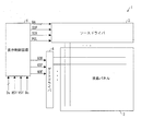
- FIG. 3 is a block diagram showing a schematic configuration of the liquid crystal display device according to the present embodiment.
- the liquid crystal display device 1 includes a liquid crystal panel 2 (display panel), a source driver 3 (data signal line driving circuit), a gate driver 4 (scanning signal line driving circuit), and a display control circuit 5.
- the source driver 3 drives the data signal line
- the gate driver 4 drives the scanning signal line
- the display control circuit 5 controls the source driver 3 and the gate driver 4.
- a CS driver retention capacitor line drive circuit for driving the retention capacitor line may be provided as necessary.
- the display control circuit 5 controls a display operation from a digital video signal Dv representing an image to be displayed, a horizontal synchronization signal HSY and a vertical synchronization signal VSY corresponding to the digital video signal Dv, from an external signal source (for example, a tuner). For receiving the control signal Dc.
- the display control circuit 5 also uses the data start pulse signal SSP as a signal for displaying the image represented by the digital video signal Dv on the display screen of the liquid crystal panel 2 based on the received signals Dv, HSY, VSY, and Dc.
- the digital video signal Dv input from an external signal source and the digital image signal DA corresponding to the digital video signal Dv are referred to as an “input image”.
- a digital image signal DA corrected based on a digital video signal Dv (input image) input from an external signal source is referred to as a “corrected image” (details will be described later). Therefore, the digital image signal DA output from the display control circuit 5 shown in FIG. 3 includes the input image and the corrected image.
- the digital image signal DA input image, corrected image
- the signal POL for controlling the polarity of the signal potential data signal potential
- the data start pulse signal The SSP and the data clock signal SCK are input to the source driver 3, and the gate start pulse signal GSP, the gate clock signal GCK, and the gate driver output control signal GOE are input to the gate driver 4.
- the source driver 3 Based on the digital image signal DA, the data clock signal SCK, the data start pulse signal SSP, and the polarity inversion signal POL, the source driver 3 has an analog potential (corresponding to a pixel value in each scanning signal line of the image represented by the digital image signal DA). Signal potential) is sequentially generated every horizontal scanning period, and these data signals are output to the data signal lines.
- the liquid crystal display device 1 having the above-described configuration has display unevenness that appears on the display screen of the liquid crystal panel 2 by providing a function of performing display using a corrected image corrected based on an input image ((a) in FIG. 28). , (See (a) of FIG. 29) can be reduced. Details of the display control circuit 5 that generates the corrected image will be described below.
- FIG. 1 is a block diagram showing a detailed configuration of the display control circuit 5.
- the display control circuit 5 includes an image input unit 51, an image determination processing unit 52, a corrected image storage unit 53, an image conversion unit 54, a timing control unit 55, a corrected image generation unit 56, and an image output. A portion 57 is provided.
- the solid line arrow in FIG. 1 shows the flow of the image data signal.
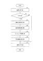
- FIG. 2 is a flowchart showing the operation of the display control circuit 5.
- the image input unit 51 receives an input image from an external signal source (for example, a tuner) and outputs it to the image determination processing unit 52 (S1: image acquisition step).
- an external signal source for example, a tuner
- the image determination processing unit 52 recognizes the input image input to the image input unit 51 and performs a determination process as to whether or not the input image needs to be corrected (S2: determination step).
- the image determination processing unit 52 determines that correction is necessary (YES in S2)
- the image determination processing unit 52 acquires a pattern image corresponding to the recognized input image from the corrected image storage unit 53, and acquires the image conversion unit 54. And an input image is output to the timing control unit 55 (S3: corrected image acquisition step).
- S3 corrected image acquisition step
- the process of acquiring the pattern image is not performed and the input image is output to the image output unit 57.
- a specific determination method in the image determination processing unit 52 and a specific example of the pattern image stored in the corrected image storage unit 53 will be described later.
- the image conversion unit 54 performs data conversion processing such as decoding on the pattern image received from the image determination processing unit 52, and outputs the converted pattern image to the corrected image generation unit 56 (S4: image conversion processing step). ). If the pattern image is not compressed data, the image conversion unit 54 may be omitted.
- the timing control unit 55 gives a delay generated by the processing of the image conversion unit 54 to the input image received from the image determination processing unit 52. Then, the timing control unit 55 outputs the input image to the corrected image generation unit 56 at the same timing as the timing at which the pattern image is output from the image conversion unit 54 (S5: timing adjustment step).
- the correction image generation unit 56 generates a correction image based on the received pattern image and input image, and outputs the correction image to the image output unit 57 (S6: correction image generation step).
- the image output unit 57 outputs the generated corrected image to the source driver 3 based on the horizontal synchronization signal HSY, the vertical synchronization signal VSY, and the control signal Dc (S7: image output process).
- the display control circuit 5 determines that the image determination processing unit 52 does not need to correct an input image input from an external signal source (NO in S2).
- the input image received from 52 is output to the source driver 3 (S7: image output step).
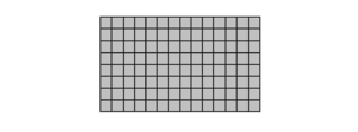
- an input image input from an external signal source is a so-called solid image that is a uniform image on the entire display screen.
- the liquid crystal display device 1 has a structure in which two color filters are arranged side by side.
- the left and right color filters are displayed on the display screen of the display panel.
- a boundary luminance difference
- the left-right luminance difference is visually recognized in a region (center portion) corresponding to the joint portion of the filter.
- the left-right luminance difference is smaller than 0.5 gradation as shown in FIG. 29A, by performing conventional gradation correction, as shown in FIG. The brightness difference between the two becomes larger, and the display quality becomes lower than before the correction.
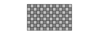
- FIG. 4 illustrates a display state of the display screen using the corrected image according to the first embodiment.
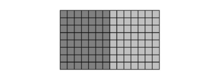
- the corrected image corresponds to a checkered pattern image. Note that one square in the figure (the same applies to the following figures) corresponds to one pixel.
- FIG. 5 shows the display state of the display screen when this correction process is not performed.
- the image determination processing unit 52 determines whether or not the input image needs to be corrected. Specifically, when the A gradation is equal to or lower than a predetermined gradation, it is determined that “correction is required”, and when it is greater than the predetermined gradation, it is determined that “correction is not required”.
- the predetermined gradation is set to a low gradation value.
- the predetermined gradation can be set in advance based on the visual recognition level of the luminance boundary according to the characteristics of the liquid crystal panel 2 (color filter characteristics, viewing angle characteristics, temperature characteristics, etc.). In this embodiment, it is assumed that the predetermined gradation is set to 31 gradations.
- the image determination processing unit 52 determines that the input image is “correction required”, A pattern image corresponding to the input image is acquired from the corrected image storage unit 53 and output to the image conversion unit 54. At the same time, the image determination processing unit 52 outputs the input image to the timing control unit 55.
- the pattern image is composed of a mixture of two gradation pixels having different gradations.
- the pattern image according to the present embodiment is configured as a checkered image by alternately arranging the pixels of the above two gradations vertically and horizontally on the entire display screen.
- the A1 gradation can be preset according to the characteristics of the liquid crystal panel 2 (color filter characteristics, viewing angle characteristics, temperature characteristics, etc.).
- the corrected image storage unit 53 can store a plurality of pattern images set in advance according to the input image.
- the two gradations in the pattern image do not use the A gradation corresponding to the input image, and are set based on the characteristics of the color filter.
- the A1 gradation (A1 gradation A gradation ⁇ ⁇ gradation) )
- A2 gradation (A2 gradation A gradation ⁇ ⁇ gradation).
- the pattern image may be configured by mixing and arranging pixels of three or more gradations having different gradations.
- the pattern image input to the image conversion unit 54 is subjected to data conversion processing such as decoding, and input to the corrected image generation unit 56.
- the input image input to the timing controller 55 is input to the corrected image generator 56 after timing adjustment.
- the corrected image generation unit 56 generates a corrected image based on the input pattern image and the input image. Specifically, a corrected image can be generated by adding and subtracting the pattern image and the input image. The generated corrected image is input to the source driver 3 via the image output unit 57, and a normal display operation is performed to display the image shown in FIG. In the first embodiment, since the pattern image is displayed on the entire display screen, the corrected image corresponds to the pattern image.
- the luminance difference between the left and right sides of the display screen shown in FIG. 6 is made uniform, and the luminance boundary appearing at the center portion of the display screen can be made inconspicuous.
- FIG. 6 shows the difference in luminance between the left and right, but this is particularly effective when the luminance difference is small (for example, when the gradation difference is 0.5 gradation or less).
- 7A shows an image when the left-right luminance difference on the display screen of FIG. 6 is small
- FIG. 7B schematically shows the display state of the corrected image corresponding to this image. Show. In the display screen of FIG. 7A, the luminance boundary of the central portion is conspicuous, but in the display screen of FIG. 7B, the luminance difference between the left and right is made uniform and the luminance boundary of the central portion becomes inconspicuous.
- the image determination processing unit 52 performs “ It is determined that no correction is necessary, and the input image is output to the image output unit 57. Thereby, display is performed based on the input image corresponding to the A gradation.
- FIG. 8A shows an image to be displayed, in which the luminance (gradation) of the central area of the display screen and the surrounding luminance (gradation) are different.
- a luminance boundary in the vertical direction is provided at the central portion (left and right boundaries) of each of the central area image and the peripheral area image. Will be visually recognized.
- the gradation is high (input gradation> predetermined gradation (31 gradation)) and the luminance boundary is not conspicuous.
- the above correction processing is performed.
- the pattern image (checkered pattern) is displayed only in the central region, so that the luminance boundary can be made inconspicuous as the entire display screen.
- FIG. 10A shows an image to be displayed.
- the brightness (gradation) of the central area of the display screen is different from the surrounding brightness (gradation), and the overall image has a low gradation. Is shown.
- FIG. 10B When the above correction processing is not performed on this image, as shown in FIG. 10B, a conspicuous luminance boundary is present at the central portion (right and left boundaries) of the image in the central area and the image in the outer peripheral area. Will appear.
- the above correction process is performed on the entire display screen.
- different pattern images (checkered patterns) are displayed in the central area and the outer peripheral area, and the luminance boundary can be made inconspicuous in the entire display screen.
- the corrected image storage unit 53 may be configured by an LUT in which the gradation of the input image and the gradation of the pattern image are associated in advance, and correction parameters corresponding to the gradation of the input image are stored. May be.
- the correction image generation unit 56 When the correction parameter is used, the correction image generation unit 56 generates a correction image based on the input image and the correction parameter.
- the pattern image of the present invention includes an image stored in advance in the corrected image storage unit 53 and an image corresponding to the correction parameter.
- the corrected image storage unit 53 may include a FRAS / EEPROM that is a non-volatile memory that stores a pattern image, and a DRAM that is a volatile memory that can access the FRASH / EEPROM at high speed.
- the pattern image is downloaded from the FRASH / EEPROM and stored in the DRAM.
- the FRASH / EEPROM may be provided outside the display control circuit 5.
- FIG. 12 shows a display state of the display screen using the corrected image according to the second embodiment.
- the corrected image has a pattern image (checkered pattern) only in the central portion including the luminance boundary on the display screen.
- the pattern image is displayed in a part of the region including the luminance boundary, at least the luminance boundary can be made inconspicuous.
- This embodiment is particularly effective when the luminance difference between the left and right sides of the display screen is small.
- correction processing is performed only for a part of the region including the luminance boundary, side effects due to correction can be minimized. That is, for example, when realizing a pseudo 10-bit display performance by using a 2-bit pseudo-gradation technique for an 8-bit source driver, there is a gradation representation capability of 1020 gradations when nothing is corrected. However, if the setting is made so that the input of 124 gradations is corrected to 126 gradations, the input of 125 gradations to 1020 gradations is corrected to 127 to 1020 gradations. Since the number of gradations that can be output is reduced compared to the above, the gradation expression ability is reduced. In this regard, according to the above configuration, correction processing is partially performed, so that it is possible to minimize a reduction in gradation expression capability.
- the luminance difference between the left and right sides of the display screen changes according to the gradation of the input image.
- the luminance difference increases as the gradation of the input image decreases, and the luminance difference decreases as the gradation of the input image increases. Therefore, the pattern image range can be changed according to the gradation of the input image.
- a pattern image is displayed on the entire display screen as in the first embodiment (see FIG. 4), while a high gradation input image is input. In this case, the pattern image is displayed only in the center portion of the display screen as in the second embodiment (see FIG. 12).
- the correction processing can be realized by the image determination processing unit 52 determining the gradation level of the input image and storing the pattern image corresponding to the gradation level in the correction image storage unit 53 in advance.
- 13A to 13D show pattern images corresponding to the gradation levels of the input image. For example, when the gradation level is set to 4 levels (the gradation increases as the level increases) and the gradation of the input image is level 4 (maximum gradation), the pattern image shown in FIG. 13A is selected. When the level is 3, the pattern image shown in (b) is selected. When the level is 2, the pattern image shown in (c) is selected. When the level is 1 (lowest gradation), the pattern shown in (d) is selected. An image is selected. According to this configuration, since the correction range can be changed according to the gradation of the input image, efficient correction processing can be performed.
- FIG. 14 illustrates a display state of the display screen using the corrected image according to the third embodiment.
- the corrected image is a pattern image (checkered pattern) in the center portion including the luminance boundary on the display screen, and the other portion is a tone-corrected image (tone-corrected image). Yes.
- the luminance boundary can be made inconspicuous, and gradation correction is performed for other display unevenness regions.
- the brightness can be made uniform over the entire display screen. This embodiment is particularly effective when the luminance difference between the left and right sides of the display screen is large (when there is a luminance difference of one gradation or more).
- the gradation of the input image (solid image) is assumed to be a gradation, and the correction process is not performed, as shown in FIG. It is assumed that the luminance on the left side corresponds to (a-1.5) gradation (darker than the right side). That is, the target luminance is displayed on the right side of the display screen, but is lower (darker) by the luminance corresponding to 1.5 gradations than the target luminance on the left side.
- an image corresponding to the left side of the display screen is composed of pixels of input gradation (a gradation) and pixels of (a + 1.0) gradation
- An image corresponding to the right side of the display screen is composed of pixels of input gradation (a gradation) and pixels of (a-1.0) gradation.
- an image in which the input gradation (a gradation) is corrected to (a + 1.0) gradation is displayed in the left area of the display screen, and an a gradation image is displayed in the right area without correction.
- the area on the left side of the display screen is decreased by a luminance corresponding to 1.5 gradations, so that the luminance corresponding to (a-0.5) gradations is obtained.
- the luminance is represented by the luminance corresponding to the a gradation.
- the input gradation (a gradation) may be corrected to (a + 2.0) gradation.
- the display state on the left side after correction is (a + 0.5) on the display screen. ) Expressed by luminance corresponding to gradation.
- FIG. 16 illustrates a display state of the display screen using the corrected image according to the fourth embodiment.
- the corrected image is a pattern image over substantially the entire display area.
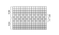
- the pattern image here is a checkered image in which the central portion including the luminance boundary on the display screen (pixels of two gradations having different gradations are alternately arranged), and in other parts, The image is represented so that the mixture ratio of the two gradation pixels decreases as the distance from the center portion increases.
- the luminance boundary can be made inconspicuous, and the luminance can be made uniform throughout the display screen.
- the central region including the luminance boundary includes a pixel for displaying the a gradation and b.
- a checkered pattern (checkered image) made up of pixels displaying gradations is displayed, and in the left region, the proportion of pixels displaying luminance corresponding to the gradation a decreases from the central region to the left end ( In the right region, the ratio of pixels displaying luminance corresponding to the b gradation (decreasing the mixture ratio) decreases from the center region to the right end.
- the mixing ratio between the pixel displaying the luminance corresponding to the a gradation and the pixel displaying the luminance corresponding to the b gradation can be set according to the gradation of the input image. For example, when the gradation of the input image is a low gradation with a large difference in luminance between the left and right sides of the display screen, the above mixing ratio is increased (for example, the luminance corresponding to the a gradation on the left side of FIG. 17B). When the gradation of the input image is a high gradation with a small luminance difference between the left and right sides of the display screen, the above mixture ratio is reduced (for example, on the left side of FIG. 17B). A small number of pixels displaying luminance corresponding to the a gradation are arranged).
- the image of the central part is not limited to the checkered image. That is, the corrected image according to the present embodiment may be configured such that the mixture ratio of the two gradation pixels decreases as the distance from the luminance boundary increases. Furthermore, the pattern image may be configured by mixing and arranging pixels of three or more gradations having different gradations.
- FIG. 18 illustrates a display state of the display screen using the corrected image according to the fifth embodiment.
- a region including at least a luminance boundary on the display screen has gradations (particularly high gradations) different from the gradation of the input image and the gradation corresponding to the luminance of the display screen. It is a pattern image.
- the luminance boundary can be made inconspicuous, and the display quality in the low gradation region can be improved.
- the right side of the display screen is a gradation, as shown in FIG. If the left side is luminance corresponding to b gradation, as shown in FIG. 19 (b), c gradation (a gradation and b gradation) is formed in the central region including the luminance boundary. Pattern image having a higher gradation).
- the c gradation is set according to the gradation of the input image, and may be (a + 1) gradation or (a + 2) gradation.
- the pattern image of the present embodiment may be configured such that the proportion of pixels displaying the c gradation becomes smaller as the distance from the luminance boundary increases.
- the pattern image of this embodiment can be set according to the luminance difference between the left and right and the gradation of the input image. For example, when the luminance on the left side is low (dark), the ratio of the pixels displaying the c gradation is configured such that the left side is larger than the right side (see FIG. 21A), or the c1 gradation is displayed on the left side.
- a configuration in which pixels are arranged and a pixel for displaying the c2 gradation on the right side (c1 gradation> c2 gradation) (see FIG. 21B) or a combination of these can be employed.
- the luminance boundary due to the seam of the color filter is exemplified as the luminance boundary on the display screen.
- the luminance boundary corresponding to the predetermined area of the present invention is not limited to this.
- a configuration example of a liquid crystal display device in which a luminance boundary may occur on the display screen will be described.
- FIG. 22 is a block diagram showing a schematic configuration of a liquid crystal display device according to another configuration example of the present embodiment.
- the liquid crystal display device 1a includes a liquid crystal panel 2a divided into a first region and a second region, a first display control circuit 5x, a first source driver SDx, a first gate driver GDx, a first Cs ( Storage capacitor wiring) control circuit CSx, second display control circuit 5y, second source driver SDy, second gate driver GDy, and second Cs control circuit CSy.
- the first display control circuit 5x, the first source driver SDx, the first gate driver GDx, and the first Cs control circuit CSx are for driving the first region
- the second display control circuit 5y, the second source driver SDy, The second gate driver GDy and the second Cs control circuit CSy are for driving the second region.
- the first display control circuit 5x receives, from an external signal source (for example, a tuner), a digital video signal Dv (x) representing an image to be displayed and a horizontal synchronization signal HSY (x) corresponding to the digital video signal Dv (x). ) And the vertical synchronization signal VSY (x) and the control signal Dc (x) for controlling the display operation.
- the second display control circuit 5y receives, from an external signal source (for example, a tuner), a digital video signal Dv (y) representing an image to be displayed and a horizontal synchronization signal HSY (y) corresponding to the digital video signal Dv (y). ) And the vertical synchronization signal VSY (y) and the control signal Dc (y) for controlling the display operation.
- the first display control circuit 5x outputs a gate start pulse GSP (x) for the first region to the first gate driver GDx, and outputs a Cs control signal for the first region to the first Cs control circuit CSx.
- the second display control circuit 5y outputs a second region gate start pulse GSP (y) or the like to the second gate driver GDy, and outputs a second region Cs control signal to the second Cs control circuit CSy.
- the first Cs control circuit CSx supplies a Cs signal (retention capacitor wiring signal) to each storage capacitor line in the first region, and the second Cs control circuit CSy supplies a Cs signal to each storage capacitor wire in the second region.
- each of the first display control circuit 5x and the second display control circuit 5y includes digital image signals DA (x) and DA (y) in each of the first source driver SDx and the second source driver SDy. Various signals shown in 3 are output.
- the liquid crystal panel 2a is provided with one data signal line corresponding to the upper half (upstream side of the panel) of one pixel column, and 1 corresponding to the lower half (downstream side of the panel) of this pixel column.
- Double-speed having a so-called upper and lower divided single source structure (two upper and lower data signal lines are provided per pixel column and two scanning signal lines are selected at the same time) provided with two data signal lines It can be driven. This will be specifically described below.
- FIG. 23 is an equivalent circuit diagram showing a part of the liquid crystal panel 2a.
- the data signal lines SLx (a), SLx (b), SLx (c), SLx (d) are arranged in this order in the first region, and the row direction (in the drawing)
- the scanning signal lines GLx (1), GLx (2), ..., GLx (k), ..., GLx (n-1), GLx (n) extending in the left-right direction are arranged in this order, and each scanning signal line GLx , CSx (k),..., CSx (n ⁇ 1), CSx (n) are arranged in this order in correspondence with the storage capacitor lines CSx (1), CSx (2),.
- k is an integer of 1 to n (1 ⁇ k ⁇ n)
- n is, for example, 540 (line).
- the pixel Px (a1) is provided corresponding to the intersection of the data signal line SLx (a) and the scanning signal line GLx (1), and the data signal line SLx (a) and the scanning signal line GLx (2 ) Is provided corresponding to the intersection of the data signal line SLx (a) and the scanning signal line GLx (k), and the pixel Px (ak) is provided corresponding to the intersection of the scanning signal line GLx (k).
- a pixel Px (bk) is provided corresponding to the intersection of the data signal line SLx (b) and the scanning signal line GLx (k).
- Each pixel Px is provided with one pixel electrode PDx, and the pixel electrode PDx (a1) of the pixel Px (a1) is connected to the data signal line SLx via the transistor Tx (a1) connected to the scanning signal line GLx (1).
- the pixel electrode PDx (a2) of the pixel Px (a2) is connected to the data signal line SLx (a) via the transistor Tx (a2) connected to the scanning signal line GLx (2).
- the pixel electrode PDx (ak) of Px (ak) is connected to the data signal line SLx (a) via the transistor Tx (ak) connected to the scanning signal line GLx (k).
- the pixel electrode PDx (bk) of the pixel Px (bk) is connected to the data signal line SLx (b) via the transistor Tx (bk) connected to the scanning signal line GLx (k).
- the data signal lines SLy (a), SLy (b), SLy (c), SLy (d) are arranged in this order, and the row direction (the left-right direction in the figure).
- GLY (k),..., GLY (n ⁇ 1), GLY (n) are arranged in this order and correspond to each scanning signal line Gly.
- the storage capacitor lines CSy (1), CSy (2),..., CSy (k),..., CSy (n ⁇ 1), CSy (n) are arranged in this order.
- k is an integer of 1 to n (1 ⁇ k ⁇ n)
- n is, for example, 540 (line).
- the pixel Py (a1) is provided corresponding to the intersection of the data signal line SLy (a) and the scanning signal line GLy (1), and the data signal line SLy (a) and the scanning signal line GLy (2 ) Corresponding to the intersection of the pixel signal Py (a2) and the pixel Py (ak) corresponding to the intersection of the data signal line SLy (a) and the scanning signal line GLy (k).
- Pixel Py (an-1) is provided corresponding to the intersection of SLy (a) and scanning signal line GLy (n-1), and the intersection of data signal line SLy (a) and scanning signal line Gly (n).
- a pixel Py (bk) is provided corresponding to the intersection of the data signal line SLy (b) and the scanning signal line GLy (k).
- each pixel electrode PDy is arranged for each pixel Py, and each pixel electrode PDy is connected to the data signal line SLy via a transistor Ty connected to the scanning signal line GLy.
- the scanning signal lines GLx and GLy are selected one by one in order, and the scanning direction in the first region and the scanning direction in the second region coincide with each other, and the first and second regions in the scanning direction in this order. Are lined up. In FIG. 23, scanning is performed from the upper side (upstream) to the lower side (downstream).
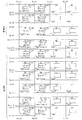
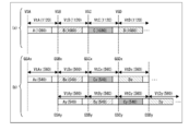
- FIG. 24A shows the input timing of frames A to D.
- the vertical synchronizing signals of frames A to D are VSA to VSD, and the periods (VtA to VtD) of frames A to D are shown. ) Is equally 1120 lines (of which the blanking period is 40 lines).
- FIG. 24B shows the timing of the write operation in the liquid crystal display device 1a.
- the second half Ay of the first frame A is written in the second area.
- the first half Bx of the second frame B is written to the first area so as to overlap with the writing period of the second half Ay of the frame A, and then the second half By of the second frame B is written to the second area.
- the first half Cx of the third frame C is written to the first area so that it overlaps the writing period of the second half By of this frame B, and then the second half Cy of the third frame C is written to the second area.
- the gate start pulse of the first half frame Ax is GSAx
- the gate start pulse of the first half frame Bx is GSBx
- the gate start pulse of the first half frame Cx is GSCx
- the gate start pulse of the first half frame Dx is GSDx.
- the gate start pulse of the frame Ay is GSAy
- the gate start pulse of the second half frame By is GSBy
- the gate start pulse of the second half frame Cy is GSCy
- the gate start pulse of the second half frame Dy is GSDy.
- the gate start pulse GSAx of the first half frame Ax and the vertical synchronization signal VSA of the frame A are synchronized
- the gate start pulse GSAy of the second half frame Ay, the gate start pulse GSBx of the first half frame Bx, and the vertical synchronization signal VSB of the frame B are The gate start pulse GSBy of the second half frame
- the gate start pulse GSCx of the first half frame Cx, and the vertical synchronization signal VSC of the frame C are synchronized
- the gate start pulse GSCy of the second half frame Cy and the gate start pulse GSDx of the first half frame Dx are synchronized.
- the vertical synchronization signal VSD of the frame D are synchronized.
- the periods (VtAx to VtDx) of the first half frames Ax to Dx are equally set to 560 lines (of which the blanking period is 20 lines).
- the liquid crystal display device 1a of the screen division (upper and lower division) driving method for example, it is only necessary to output (scan) 540 lines during an input period of 1080 lines.
- 1H (one horizontal scanning period) on the output side can be doubled by 1H (one horizontal scanning period) on the input side, the charging rate of each pixel can be increased.
- the writing time to each pixel can be shortened with the high definition of the liquid crystal display device.
- the portion to be divided (the boundary between the first region and the second region) is not limited to the center in the vertical direction of the liquid crystal panel, and the areas of the first region and the second region may be different. In this case, a part of the frame is written in the first area, and the remainder of the frame is written in the second area.
- V inversion drive method The liquid crystal display device 1a is driven by the V inversion driving method. For example, a data signal whose polarity is inverted every one vertical scanning period (1V) is supplied to the data signal line, while data signals having opposite polarities are supplied to two adjacent data signal lines in the same horizontal scanning period. It is driven by 1V inversion driving method. In the V inversion driving method in the liquid crystal display device 1a, data signals having the same polarity may be supplied to two adjacent data signal lines in the same horizontal scanning period.
- the pixel potential increases toward the end side in the scanning direction due to the parasitic capacitance (Csd) generated between the data signal line and the pixel electrode.
- Csd parasitic capacitance
- the luminance decreases due to a decrease in the potential of the written data signal. For example, if the image to be displayed is a solid white image, the display screen becomes darker as it goes to the end side in the scanning direction as shown in FIG.
- the V inversion driving method when the V inversion driving method is applied to the screen division driving method, the end side of the first area where the luminance decreases and the starting end side of the second area displayed at the original luminance are adjacent to each other.
- the image to be displayed is a solid white image, as shown in FIG. 26, the luminance change (luminance boundary) becomes remarkable at the boundary between the first region and the second region, and the display quality is deteriorated.
- the luminance boundary in the first region and the second region can be made inconspicuous by performing the correction process shown in each of the above examples according to the present embodiment. Decline can be prevented.
- FIG. 27 illustrates a display screen when the correction process according to the second embodiment is performed.
- the brightness boundary can be made inconspicuous by displaying a checkered pattern image on each of the end side (lower part) of the first region and the start side (upper part) of the second region. .
- the first display control circuit 5x and the second display control circuit 5y in the liquid crystal display device 1a can have the same configuration as the display control circuit 5 shown in FIG. Therefore, the corrected image corresponding to the first area can be generated in the first display control circuit 5x, and the corrected image corresponding to the second area can be generated in the second display control circuit 5y.
- the luminance boundary in the vertically divided drive type liquid crystal display device is shown, but as another configuration example, a liquid crystal display device provided with a plurality of adjacent source drivers can be cited.
- a luminance boundary can be visually recognized at a joint portion of a plurality of display areas that each source driver is responsible for.
- the luminance boundary between the display areas can be made inconspicuous by performing the correction processing according to the above-described embodiments.
- the luminance boundary can be made inconspicuous by performing the correction processing according to the above-described embodiments.
- the pattern image may be displayed in all areas within the at least some area.
- the pattern image may be displayed only in the predetermined area in the at least some area.
- correction processing is performed only for a part of the region including the luminance boundary, so that it is possible to minimize a reduction in gradation expression capability due to correction (details will be described later).
- the pattern image is displayed in the predetermined area in the at least some area, and the display brightness outside the predetermined area is uniform outside the predetermined area. In this way, a gradation corrected image obtained by correcting the input gradation corresponding to the input image can be displayed.
- the luminance boundary can be made inconspicuous, and gradation correction is performed for other display unevenness regions.
- the brightness can be made uniform throughout the display screen.
- the pattern image may be a checkered pattern image.
- the pattern image is configured by mixing and arranging pixels of two gradations having different gradations, and in at least a part of the area, the pattern image is separated from the predetermined area.
- a configuration in which the mixing ratio of the two gradation pixels is small can also be adopted.
- the luminance boundary can be made inconspicuous, and the luminance can be made uniform throughout the display screen.
- the display image displayed on the display screen with respect to the input gradation corresponding to the input image is represented by the luminance corresponding to the first gradation and the second gradation.
- the pattern image may include pixels that display the first gradation and pixels that display the second gradation.
- the display image displayed on the display screen with respect to the input gradation corresponding to the input image is represented by the luminance corresponding to the first gradation and the second gradation.
- the pattern image may be composed of pixels that display gradations higher than the first gradation and the second gradation.
- the luminance boundary can be made inconspicuous, and the display quality can be enhanced particularly in the low gradation region.
- the pattern image is a case where an image having the same gradation is displayed in at least a part of the display screen, and the input image has a low gradation.
- it may be configured to be displayed in at least a predetermined area in the area.
- the display device may include a plurality of color filters arranged adjacent to each other, and the predetermined region may include a joint portion of each color filter.
- the luminance boundary visually recognized in the display area corresponding to the seam portion of the color filter can be made inconspicuous.
- data signal lines, scanning signal lines, and pixels are formed in the first and second regions provided in the display panel, respectively, and a part of the current frame is written in the first region.
- the remainder of the current frame is written in the second area, the scanning direction in the first area and the scanning direction in the second area coincide with each other, and the first and second areas are in the scanning direction.
- These predetermined regions may be arranged in this order, and the predetermined region may include a boundary portion between the first region and the second region.
- the luminance boundary visually recognized in the display area corresponding to the boundary portion between the first area and the second area can be made inconspicuous.
- the determination step determines that correction is necessary when the input gradation corresponding to the input image is equal to or lower than a predetermined gradation. If it is too large, it may be determined that correction is not necessary.
- a display when it is determined that there is no need to correct in the determination step, a display can be performed based on the input image.
- the display device is A display device that displays an input image corresponding to the input image data on a display screen based on the input image data, When displaying an image of the same gradation in at least a partial area of the display screen, a pattern image preset according to the input image is displayed in at least a predetermined area in the area, and Outside the predetermined area, a gradation-corrected image in which the input gradation corresponding to the input image is corrected so that the display brightness outside the predetermined area is uniform is displayed.
- the display device is A display device that displays an input image corresponding to the input image data on a display screen based on the input image data, When displaying an image of the same gradation in at least a partial area of the display screen, a pattern image preset according to the input image is displayed in at least a predetermined area in the area, The pattern image is configured by mixing and arranging pixels of two gradations having different gradations, and the mixture of the pixels of the two gradations is further away from the predetermined area in the at least a part of the area. The ratio is small.
- the driving method of the display device is as follows.
- a correction image generation step of generating a correction image based on the pattern image acquired in the correction image acquisition step and the input image received in the image acquisition step;
- display is performed based on the corrected image,
- the corrected image is a pattern image that is displayed in advance in at least a predetermined area in the area when an image of the same gradation is displayed in at least a part of the area of the display screen.
- a gradation-corrected image that is displayed outside the predetermined area and that corrects the input
- the driving method of the display device is as follows.
- a correction image generation step of generating a correction image based on the pattern image acquired in the correction image acquisition step and the input image received in the image acquisition step;
- display is performed based on the corrected image
- the determination step determines that correction is necessary when the input gradation corresponding to the input image is equal to or lower than a predetermined gradation, and determines that correction is not necessary when the input gradation is larger than the predetermined gradation. It is characterized by.
- the present invention is suitable for a liquid crystal television, for example.
Landscapes
- Engineering & Computer Science (AREA)
- Physics & Mathematics (AREA)
- Computer Hardware Design (AREA)
- General Physics & Mathematics (AREA)
- Theoretical Computer Science (AREA)
- Chemical & Material Sciences (AREA)
- Crystallography & Structural Chemistry (AREA)
- Control Of Indicators Other Than Cathode Ray Tubes (AREA)
Abstract
表示画面に入力画像データに応じた入力画像を表示する液晶表示装置において、表示画面に同一階調の画像を表示する場合、輝度境界の部分に、市松模様のパターン画像を表示する。これにより、表示ムラを確実に低減して、表示品位を高めることができる表示装置及びその駆動方法を提供する。
Description
本発明は、液晶表示装置等の表示装置及びその駆動方法に関する。
従来、表示装置において、製造誤差に起因した表示画面に発生する表示ムラが問題となっている。
例えば、大型の表示パネルでは、その構造上、カラーフィルタが左右2枚に分割されている。それぞれのカラーフィルタにおいて製造上の誤差が存在する場合、表示パネルの表示画面において、2枚のカラーフィルタの継ぎ目部分に相当する領域に、境界(輝度差)が視認されることになる。
図28の(a)は、表示パネルの表示画面において、輝度差が存在する場合の表示状態を示す図である。表示パネルには、左側の領域には左用のカラーフィルタが配置されており、右側の領域には右用のカラーフィルタが配置されている。これら左右のカラーフィルタに製造上の誤差が存在する場合、図28の(a)に示すように、左右のカラーフィルタの継ぎ目部分に相当する中央部分に、境界(輝度差)が視認される。
従来、上記表示ムラ(輝度差)を低減するための技術として、階調補正を行う表示装置が提案されている。具体的には、表示画面の左右で輝度差がある場合に、一方の輝度を他方の輝度に合わせるように階調補正を行うものである。例えば、図28の(a)に示すように、表示画面の左側の領域の輝度が、右側の領域の輝度よりも低い(暗い)場合は、左側の領域の輝度が高く(明るく)なるように、左側の領域に対応するデータ信号(入力画像)の階調値を上げる。これにより、図28の(b)に示すように、左右で表示輝度が均一化され、表示ムラを低減することができる。
また、特許文献1の表示装置では、表示画面上における矩形領域の大きさと位置を指定し、その範囲を階調補正するとともに、その周辺部の階調変化を縦方向及び横方向に徐々に減少させることにより、表示ムラを低減している。
しかしながら、従来の技術では、階調を補正しているため、輝度の調整幅に限界がある。つまり、階調単位で補正しているため、例えば、表示画面において、左右の輝度の差が、1階調よりも小さい差であった場合は、階調を補正しても、左右の輝度を合わせることはできない。特に、左右の輝度の差が、0.5階調よりも小さい差であった場合は、階調を補正することにより、左右の輝度の差が大きくなってしまい、補正前よりも表示品位が低下してしまう。図29の(a)には、表示画面の左右の輝度の差が、0.5階調よりも小さい場合を模式的に示しており、表示画面の左側の領域が右側の領域よりも僅かに暗くなっている。この場合に、従来の階調補正、例えば左側の領域だけを1階調上げる補正を行う(右側の領域は補正しない)と、左右の明暗が逆転し、図29の(b)に示すように、表示画面の左側の領域が右側の領域よりも明るくなる。そして、補正後の表示画面(図29の(b))の左右の輝度の差が、補正前の表示画面(図29の(a))の左右の輝度の差よりも大きくなり、補正前よりも表示品位が低下してしまう。
特に、近年では大型表示パネルにおける製造技術等の発達により、製造上の誤差により生じる輝度差は小さくなっており、従来の技術では、表示ムラを確実に低減することは困難である。
本発明は、上記問題点に鑑み、表示ムラを確実に低減して、表示品位を高めることができる表示装置及びその駆動方法を提供することにある。
本発明に係る表示装置は、上記課題を解決するために、
入力された入力画像データに基づいて、表示画面に該入力画像データに応じた入力画像を表示する表示装置であって、
上記表示画面の少なくとも一部の領域に同一階調の画像を表示する場合、該領域内の少なくとも所定領域に、上記入力画像に応じて予め設定されたパターン画像を表示することを特徴とする。
入力された入力画像データに基づいて、表示画面に該入力画像データに応じた入力画像を表示する表示装置であって、
上記表示画面の少なくとも一部の領域に同一階調の画像を表示する場合、該領域内の少なくとも所定領域に、上記入力画像に応じて予め設定されたパターン画像を表示することを特徴とする。
上記の構成によれば、例えば表示画面に同一階調の画像(いわゆるベタ画像)を表示する際に輝度境界(表示ムラ)が視認される場合、輝度境界の部分に、予め設定されたパターン画像を表示することができる。ここで、パターン画像は、例えば、表示輝度に対応する2つの階調からなる市松模様とすることができる。このパターン画像を輝度境界の部分に表示することにより、輝度境界を目立たなくすることができる。
表示ムラを低減するための上記の補正処理は、従来の階調補正とは異なり、微小な輝度差(例えば、1階調以下の輝度差)に対しても有効である。よって、表示ムラを確実に低減して、表示品位を高めることができる。
本発明に係る表示装置の駆動方法は、上記課題を解決するために、
入力された入力画像データに基づいて、表示画面に該入力画像データに応じた入力画像を表示する表示装置の駆動方法であって、
外部から上記入力画像を受け取る画像取得工程と、
上記受け取った入力画像を認識するとともに、該入力画像を補正する必要があるか否かの判定処理を行う判定工程と、
上記判定工程において補正する必要があると判定した場合に、上記認識した入力画像に対応する、予め記憶部に格納されたパターン画像を取得する補正画像取得工程と、
上記補正画像取得工程において取得したパターン画像と、上記画像取得工程において受け取った入力画像とに基づき、補正画像を生成する補正画像生成工程とを含み、
上記判定工程において補正する必要があると判定した場合は、上記補正画像に基づいて表示を行うことを特徴とする。
入力された入力画像データに基づいて、表示画面に該入力画像データに応じた入力画像を表示する表示装置の駆動方法であって、
外部から上記入力画像を受け取る画像取得工程と、
上記受け取った入力画像を認識するとともに、該入力画像を補正する必要があるか否かの判定処理を行う判定工程と、
上記判定工程において補正する必要があると判定した場合に、上記認識した入力画像に対応する、予め記憶部に格納されたパターン画像を取得する補正画像取得工程と、
上記補正画像取得工程において取得したパターン画像と、上記画像取得工程において受け取った入力画像とに基づき、補正画像を生成する補正画像生成工程とを含み、
上記判定工程において補正する必要があると判定した場合は、上記補正画像に基づいて表示を行うことを特徴とする。
以上のように、本発明に係る表示装置及びその駆動方法は、上記表示画面の少なくとも一部の領域に同一階調の画像を表示する場合、該領域内の少なくとも所定領域に、上記入力画像に応じて予め設定されたパターン画像を表示するものである。これにより、表示ムラを確実に低減して、表示品位を高めることができる表示装置及びその駆動方法を提供することができる。
本発明の実施の形態を、図面を用いて説明すれば、以下のとおりである。なお、以下では、本発明の表示装置の一例として液晶表示装置(液晶ディスプレイ)を挙げて説明するが、本発明の表示装置はこれに限定されるものではなく、有機ELディスプレイ、プラズマディスプレイ等の各種表示装置に適用することができる。
図3は、本実施の形態に係る液晶表示装置の概略構成を示すブロック図である。同図に示すように、液晶表示装置1は、液晶パネル2(表示パネル)、ソースドライバ3(データ信号線駆動回路)、ゲートドライバ4(走査信号線駆動回路)、及び、表示制御回路5を備えている。ソースドライバ3はデータ信号線を駆動し、ゲートドライバ4は走査信号線を駆動し、表示制御回路5は、ソースドライバ3及びゲートドライバ4を制御する。なお、必要に応じて保持容量配線を駆動するCSドライバ(保持容量配線駆動回路)が設けられていても良い。
表示制御回路5は、外部の信号源(例えばチューナ)から、表示すべき画像を表すデジタルビデオ信号Dvと、デジタルビデオ信号Dvに対応する水平同期信号HSY及び垂直同期信号VSYと、表示動作を制御するための制御信号Dcとを受け取る。また、表示制御回路5は、受け取ったこれらの信号Dv、HSY、VSY、Dcに基づき、デジタルビデオ信号Dvの表す画像を液晶パネル2の表示画面に表示させるための信号として、データスタートパルス信号SSPと、データクロック信号SCKと、表示すべき画像を表すデジタル画像信号DA(デジタルビデオ信号Dvに対応する信号)と、ゲートスタートパルス信号GSPと、ゲートクロック信号GCKと、ゲートドライバ出力制御信号(走査信号出力制御信号)GOEとを生成し、これらを出力する。なお、以下では、便宜上、外部の信号源から入力されたデジタルビデオ信号Dv及びこれに対応するデジタル画像信号DAを、「入力画像」と称す。また、外部の信号源から入力されたデジタルビデオ信号Dv(入力画像)に基づいて補正されたデジタル画像信号DAを、「補正画像」(詳細は後述する)と称す。よって、図3に示す表示制御回路5から出力されるデジタル画像信号DAには、入力画像及び補正画像が含まれる。
上記のようにして表示制御回路5において生成された信号のうち、デジタル画像信号DA(入力画像、補正画像)と、信号電位(データ信号電位)の極性を制御する信号POLと、データスタートパルス信号SSPと、データクロック信号SCKとは、ソースドライバ3に入力され、ゲートスタートパルス信号GSPと、ゲートクロック信号GCKと、ゲートドライバ出力制御信号GOEとは、ゲートドライバ4に入力される。
ソースドライバ3は、デジタル画像信号DA、データクロック信号SCK、データスタートパルス信号SSP、及び極性反転信号POLに基づき、デジタル画像信号DAの表す画像の各走査信号線における画素値に相当するアナログ電位(信号電位)を1水平走査期間毎に順次生成し、これらのデータ信号をデータ信号線に出力する。
上記構成を有する液晶表示装置1は、特に、入力画像に基づいて補正された補正画像による表示を行う機能を備えることにより、液晶パネル2の表示画面に出現する表示ムラ(図28の(a)、図29の(a)参照)を低減することができるものである。以下、上記補正画像を生成する表示制御回路5の詳細について説明する。
(表示制御回路5の構成)
図1は、表示制御回路5の詳細な構成を示すブロック図である。同図に示すように、表示制御回路5は、画像入力部51、画像判定処理部52、補正画像記憶部53、画像変換部54、タイミング制御部55、補正画像生成部56、及び、画像出力部57を備えている。なお、図1中の実線矢印は画像データ信号の流れを示している。また、図2は、表示制御回路5の動作を示すフロー図である。
図1は、表示制御回路5の詳細な構成を示すブロック図である。同図に示すように、表示制御回路5は、画像入力部51、画像判定処理部52、補正画像記憶部53、画像変換部54、タイミング制御部55、補正画像生成部56、及び、画像出力部57を備えている。なお、図1中の実線矢印は画像データ信号の流れを示している。また、図2は、表示制御回路5の動作を示すフロー図である。
画像入力部51は、外部の信号源(例えばチューナ)から入力画像を受け取り画像判定処理部52に出力する(S1:画像取得工程)。
画像判定処理部52は、画像入力部51に入力された入力画像を認識するとともに、該入力画像を補正する必要があるか否かの判定処理を行う(S2:判定工程)。また、画像判定処理部52は、補正する必要があると判定した場合(S2にてYESの場合)は、認識した入力画像に対応するパターン画像を補正画像記憶部53から取得し画像変換部54に出力するとともに、入力画像をタイミング制御部55に出力する(S3:補正画像取得工程)。一方、補正する必要がないと判定した場合(S2にてNOの場合)は、パターン画像を取得する処理は行わず、入力画像を画像出力部57に出力する。画像判定処理部52における具体的な判定方法、及び、補正画像記憶部53に格納されているパターン画像の具体例については後述する。
画像変換部54は、画像判定処理部52から受け取ったパターン画像に対して、復号等のデータ変換処理を行い、変換後のパターン画像を補正画像生成部56に出力する(S4:画像変換処理工程)。なお、パターン画像が圧縮データでない場合は、画像変換部54は省略されていても良い。
タイミング制御部55は、画像判定処理部52から受け取った入力画像に対して、画像変換部54の処理で発生する遅延を付与する。そして、タイミング制御部55は、入力画像を、パターン画像が画像変換部54から出力されるタイミングと同じタイミングで、補正画像生成部56に出力する(S5:タイミング調整工程)。
補正画像生成部56は、受け取ったパターン画像及び入力画像に基づき、補正画像を生成し、画像出力部57に出力する(S6:補正画像生成工程)。
画像出力部57は、水平同期信号HSY、垂直同期信号VSY、及び制御信号Dcに基づき、生成された補正画像をソースドライバ3に出力する(S7:画像出力工程)。
なお、表示制御回路5は、画像判定処理部52において、外部の信号源から入力された入力画像を補正する必要がないと判定された場合(S2にてNOの場合)は、画像判定処理部52から受け取った入力画像をソースドライバ3に出力する(S7:画像出力工程)。
次に、上記パターン画像、及び、このパターン画像に基づき生成される補正画像の具体例(実施例1~5)について説明する。なお、以下では、便宜上、外部の信号源から入力される入力画像を、表示画面全体に一様な画像である、いわゆるベタ画像とする。また、本液晶表示装置1では、2枚のカラーフィルタが左右に並んで配された構造を有するものとする。
ここで、2枚のカラーフィルタが左右に並んで配された構造を有する場合、図28の(a)及び図29の(a)に示したように、表示パネルの表示画面において、左右のカラーフィルタの継ぎ目部分に相当する領域(中央部分)に、境界(輝度差)が視認される。また、特に図29の(a)のように左右の輝度差が0.5階調よりも小さい場合は、従来の階調補正を行うことにより、図29の(b)に示すように、左右の輝度の差が大きくなってしまい、補正前よりも表示品位が低下してしまう。
これに対して、本液晶表示装置1によれば、以下の実施例1~5に示すパターン画像を用いることにより、輝度境界を目立たなくして、表示品位を高めることができる。
(実施例1)
図4には、実施例1に係る補正画像による表示画面の表示状態を示している。同図に示すように、補正画像は、市松模様の画像に対応している。なお、同図中(以降の図も同様)の1マスは1画素に対応しているものとする。
図4には、実施例1に係る補正画像による表示画面の表示状態を示している。同図に示すように、補正画像は、市松模様の画像に対応している。なお、同図中(以降の図も同様)の1マスは1画素に対応しているものとする。
ここで、図4に示す補正画像の生成方法について具体的に説明する。
まず、外部の信号源からA階調に相当する入力画像(図5)が、画像入力部51に入力されたと仮定する。なお、図6は、本補正処理を行わない場合の表示画面の表示状態を示している。
次に、画像判定処理部52は、入力画像について、補正する必要があるか否かを判定する。具体的には、A階調が、所定階調以下の場合は「補正要」と判定し、所定階調よりも大きい場合は「補正不要」と判定する。
ここで、表示画面における輝度差は、低階調の範囲(暗領域)において視認され易いため、所定階調は低階調の値に設定されていることが好ましい。例えば、最大255階調の液晶表示装置において、0階調から31階調の範囲の画像において輝度差が目立つ場合は、所定階調を31階調に設定する。なお、所定階調は、液晶パネル2の特性(カラーフィルタの特性、視野角特性、温度特性など)に応じた輝度境界の視認レベルに基づいて予め設定することができる。本実施例では、所定階調が31階調に設定されているものとする。
続いて、入力画像のA階調が31階調よりも低階調(A階調≦31階調)であった場合、画像判定処理部52は、入力画像について「補正要」と判定し、入力画像に対応するパターン画像を補正画像記憶部53から取得し画像変換部54に出力する。同時に、画像判定処理部52は、入力画像をタイミング制御部55に出力する。
ここで、パターン画像は、互いに階調が異なる2つの階調の画素が混合配置されて構成されている。本実施例に係るパターン画像は、上記2つの階調の画素が、表示画面全体において上下左右に交互に配されることにより市松模様の画像に構成されている。上記2つの階調は、例えば、入力画像に対応するA階調、及び、カラーフィルタの特性に基づき設定されたA1階調(A1階調=A階調±α階調)とすることができる。
また、上記A1階調は、予め設定することができる。具体的には、本補正処理を行わない液晶表示装置において、A階調の画像を表示させたときの表示画面の左右の輝度を測定し、一方の輝度が本来の輝度(A階調に相当する輝度)よりも低い場合は、該一方の輝度を高めるために、A1階調をA階調よりも高い階調に設定する(A1階調=A階調+α階調)。また、一方の輝度が本来の輝度(A階調に相当する輝度)よりも高い場合は、該一方の輝度を下げるために、A1階調をA階調よりも低い階調に設定する(A1階調=A階調-α階調)。このように、A1階調は、液晶パネル2の特性(カラーフィルタの特性、視野角特性、温度特性など)に応じて予め設定することができる。これにより、補正画像記憶部53には、入力画像に応じて予め設定された複数のパターン画像を格納しておくことができる。
なお、パターン画像における上記2つの階調は、入力画像に対応するA階調を使用せず、カラーフィルタの特性に基づき設定された、A1階調(A1階調=A階調±α階調)及びA2階調(A2階調=A階調±β階調)としてもよい。さらに、パターン画像は、互いに階調が異なる3つ以上の階調の画素が混合配置されて構成されていてもよい。
続いて、画像変換部54に入力されたパターン画像は、復号等のデータ変換処理が行われ、補正画像生成部56に入力される。一方、タイミング制御部55に入力された入力画像は、タイミング調整がされた後、補正画像生成部56に入力される。
補正画像生成部56では、入力されたパターン画像及び入力画像に基づいて、補正画像を生成する。具体的には、パターン画像及び入力画像を加減算することにより補正画像を生成することができる。生成された補正画像は、画像出力部57を介してソースドライバ3に入力され、通常の表示動作が行われ、図4に示す画像が表示される。本実施例1では、表示画面全体にパターン画像が表示されるため、上記補正画像はパターン画像に相当する。
上記補正画像によれば、図6に示した表示画面の左右の輝度差が均一化され、表示画面の中央部分に現れる輝度境界を目立たなくすることができる。
なお、便宜上、図6では、左右の輝度差を大きくして表しているが、輝度差が小さい場合(例えば、階調差が0.5階調以下の場合)に特に効果がある。図7の(a)は、図6の表示画面における左右の輝度差が小さい場合の画像を表しており、図7の(b)は、この画像に対応する補正画像の表示状態を模式的に示している。図7の(a)の表示画面では、中央部分の輝度境界が目立っているが、図7の(b)の表示画面では、左右の輝度差が均一化され、中央部分の輝度境界が目立たなくなっていることが分かる。
なお、上記の補正処理において、入力画像のA階調が31階調よりも高階調(A階調>31階調)であった場合は、画像判定処理部52は、入力画像に対して「補正不要」と判定し、入力画像を画像出力部57に出力する。これにより、A階調に相当する入力画像に基づき表示が行われる。
このように、本液晶表示装置1では、従来のように所定領域全体を均一に階調補正することなく、パターン画像を表示する補正処理により、微小な輝度差による表示ムラを低減することができる。
ここで、上記の説明では、表示画面全体にベタ画像を表示する場合を例に挙げたが、本実施の形態はこれに限定されるものではなく、図8の(a)に示すような、表示画面の一部の領域に同一階調の画像を表示する場合にも適用できる。図8の(a)は、表示すべき画像であって、表示画面の中央領域の輝度(階調)と、その周囲の輝度(階調)とが異なる画像を示している。この画像に対して上記補正処理を行わない場合は、図8の(b)に示すように、中央領域の画像及び外周領域の画像それぞれの中央部分(左右の境界)に、縦方向の輝度境界が視認されることになる。
図8の(b)に示す画像において、外周領域では、高階調(入力階調>所定階調(31階調))であり輝度境界が目立たないため、上記補正処理を行われない一方、中央領域では、低階調(入力階調≦所定階調(31階調))であり輝度境界が目立つため、上記補正処理が行われる。これにより、図9に示すように、中央領域のみパターン画像(市松模様)が表示されることによって、表示画面全体として輝度境界を目立たなくすることができる。
また、図10の(a)は、表示すべき画像であって、表示画面の中央領域の輝度(階調)と、その周囲の輝度(階調)とが異なり、全体として低階調の画像を示している。この画像に対して、上記補正処理を行わない場合は、図10の(b)に示すように、中央領域の画像及び外周領域の画像それぞれの中央部分(左右の境界)に、目立った輝度境界が現れることになる。
このような画像に対しては、表示画面全体として上記補正処理が行われる。これにより、図11に示すように、中央領域及び外周領域に、互いに異なるパターン画像(市松模様)が表示され、表示画面全体として輝度境界を目立たなくすることができる。
なお、補正画像記憶部53は、入力画像の階調と、パターン画像の階調とが予め関連付けられたLUTにより構成されていても良く、また、入力画像の階調に対応する補正パラメータが格納されていても良い。補正パラメータを使用する場合は、補正画像生成部56において、入力画像及び補正パラメータに基づき、補正画像が生成される。本発明のパターン画像には、補正画像記憶部53に予め格納された画像、及び、補正パラメータに対応する画像が含まれる。
また、補正画像記憶部53は、パターン画像を格納する不揮発性メモリのFRASH/EEPROMと、FRASH/EEPROMに高速アクセス可能な揮発性メモリのDRAMとを含んで構成されていても良い。この補正画像記憶部53では、電源投入後、FRASH/EEPROMからパターン画像をダウンロードし、DRAMに格納される。なお、FRASH/EEPROMは、表示制御回路5の外部に設けられていても良い。
次に、他の実施例に係る補正画像による補正処理について説明する。なお、以下では、説明の便宜上、実施例1において示した部材と同一の機能を有する部材には、同一の符号を付し、その説明を省略する。また、実施例1において定義した用語については、特に断らない限り各実施例においてもその定義に則って用いるものとする。
(実施例2)
図12には、実施例2に係る補正画像による表示画面の表示状態を示している。同図に示すように、補正画像は、表示画面における、輝度境界を含む中央部分のみがパターン画像(市松模様)となっている。
図12には、実施例2に係る補正画像による表示画面の表示状態を示している。同図に示すように、補正画像は、表示画面における、輝度境界を含む中央部分のみがパターン画像(市松模様)となっている。
この構成によれば、輝度境界を含む一部の領域にパターン画像が表示されるため、少なくとも輝度境界を目立たなくすることができる。本実施例は、特に、表示画面の左右の輝度差が小さい場合に有効である。
また、輝度境界を含む一部の領域のみ補正処理を行うため、補正による副作用を最小限に抑えることができる。すなわち、例えば8ビットのソースドライバに2ビットの擬似階調技術を使って擬似10ビットの表示性能を実現する場合、何も補正しない場合は1020階調の階調表現能力がある。しかし、ここで仮に124階調の入力を126階調に補正するような設定にした場合、125階調~1020階調の入力は127~1020階調に補正されることになり、入力階調と比べて出力できる階調の数が少なくなるため、階調表現能力が低下してしまう。この点、上記の構成によれば、部分的に補正処理を行うため、階調表現能力の低下を最小限に抑えることができる。
(実施例2の変形例)
ここで、表示画面の左右の輝度差は、入力画像の階調に応じて変化する。例えば、入力画像の階調が低いほど輝度差が大きくなり、入力画像の階調が高いほど輝度差は小さくなる。よって、入力画像の階調に応じてパターン画像の範囲を変更する構成とすることもできる。具体的には、低階調の入力画像が入力された場合は、実施例1のように、表示画面全体にパターン画像を表示する(図4参照)一方、高階調の入力画像が入力された場合は、本実施例2のように、表示画面の中央部分のみにパターン画像を表示する(図12参照)。なお、上記補正処理は、画像判定処理部52が入力画像の階調のレベル判定を行い、階調レベルに応じたパターン画像を予め補正画像記憶部53に格納しておくことにより実現できる。図13の(a)~(d)は、入力画像の階調レベルに応じたパターン画像を示している。例えば、階調レベルを4段階に設定(レベルが上がるほど高階調とする)し、入力画像の階調がレベル4(最大階調)のときは図13の(a)に示すパターン画像が選択され、レベル3のときは(b)に示すパターン画像が選択され、レベル2のときは(c)に示すパターン画像が選択され、レベル1(最低階調)のときは(d)に示すパターン画像が選択される。この構成によれば、入力画像の階調に応じて補正範囲を変えることができるため、効率的な補正処理が可能となる。
ここで、表示画面の左右の輝度差は、入力画像の階調に応じて変化する。例えば、入力画像の階調が低いほど輝度差が大きくなり、入力画像の階調が高いほど輝度差は小さくなる。よって、入力画像の階調に応じてパターン画像の範囲を変更する構成とすることもできる。具体的には、低階調の入力画像が入力された場合は、実施例1のように、表示画面全体にパターン画像を表示する(図4参照)一方、高階調の入力画像が入力された場合は、本実施例2のように、表示画面の中央部分のみにパターン画像を表示する(図12参照)。なお、上記補正処理は、画像判定処理部52が入力画像の階調のレベル判定を行い、階調レベルに応じたパターン画像を予め補正画像記憶部53に格納しておくことにより実現できる。図13の(a)~(d)は、入力画像の階調レベルに応じたパターン画像を示している。例えば、階調レベルを4段階に設定(レベルが上がるほど高階調とする)し、入力画像の階調がレベル4(最大階調)のときは図13の(a)に示すパターン画像が選択され、レベル3のときは(b)に示すパターン画像が選択され、レベル2のときは(c)に示すパターン画像が選択され、レベル1(最低階調)のときは(d)に示すパターン画像が選択される。この構成によれば、入力画像の階調に応じて補正範囲を変えることができるため、効率的な補正処理が可能となる。
なお、表示制御回路5におけるその他の処理は、実施例1と同様であるため説明を省略する。
(実施例3)
図14には、実施例3に係る補正画像による表示画面の表示状態を示している。同図に示すように、補正画像は、表示画面における、輝度境界を含む中央部分がパターン画像(市松模様)であり、その他の部分は階調補正された画像(階調補正画像)となっている。
図14には、実施例3に係る補正画像による表示画面の表示状態を示している。同図に示すように、補正画像は、表示画面における、輝度境界を含む中央部分がパターン画像(市松模様)であり、その他の部分は階調補正された画像(階調補正画像)となっている。
この構成によれば、輝度境界を含む一部の領域にパターン画像が表示されるため、輝度境界を目立たなくすることができるとともに、他の表示ムラの領域については階調補正が行われるため、表示画面全体として輝度を均一化することができる。本実施例は、特に、表示画面の左右の輝度差が大きい場合(1階調以上の輝度差がある場合)に有効である。
具体的には、例えば、入力画像(ベタ画像)の階調をa階調と仮定し、補正処理を行わない場合は図15の(a)に示すように、表示画面の右側がa階調に相当する輝度であり、左側が(a-1.5)階調に相当する輝度(右側よりも暗い)であったと仮定する。すなわち、表示画面の右側では目的の輝度が表示されているが、左側では目的の輝度よりも、1.5階調に相当する輝度だけ低く(暗く)なっている。
そこで、中央領域に表示するパターン画像については、例えば、表示画面の左側に対応する画像を、入力階調(a階調)の画素と、(a+1.0)階調の画素とで構成し、表示画面の右側に対応する画像を、入力階調(a階調)の画素と、(a-1.0)階調の画素とで構成する。これにより、表示画面の中央領域では、図15の(b)に示すように、左側では1.5階調に相当する輝度だけ低下するため、(a-1.5)階調に相当する輝度と、(a-0.5)階調に相当する輝度とで表され、右側では輝度が低下しないため、a階調に相当する輝度と、(a-1.0)階調に相当する輝度とで表される。
また、表示画面の左側の領域については、入力階調(a階調)を(a+1.0)階調に補正した画像を表示し、右側の領域については補正せずにa階調の画像を表示する。これにより、図15の(b)に示すように、表示画面の左側の領域では、1.5階調に相当する輝度だけ低下するため、(a-0.5)階調に相当する輝度で表され、右側の領域ではa階調に相当する輝度で表される。なお、左側の領域について、入力階調(a階調)を(a+2.0)階調に補正しても良く、この場合は、表示画面では、補正後の左側の表示状態は(a+0.5)階調に相当する輝度で表される。
なお、階調補正は、周知の技術を適用することができる。また、本実施例においても、図13に示したパターン画像を適用することができる。
(実施例4)
図16には、実施例4に係る補正画像による表示画面の表示状態を示している。同図に示すように、補正画像は、表示領域の略全体にわたってパターン画像となっている。ここでのパターン画像は、表示画面における、輝度境界を含む中央部分が市松模様の画像(互いに階調が異なる2つの階調の画素が交互に配置されている)であり、その他の部分では、中央部分から遠ざかる程、2つの階調の画素の混合比が小さくなるように表された画像となっている。
図16には、実施例4に係る補正画像による表示画面の表示状態を示している。同図に示すように、補正画像は、表示領域の略全体にわたってパターン画像となっている。ここでのパターン画像は、表示画面における、輝度境界を含む中央部分が市松模様の画像(互いに階調が異なる2つの階調の画素が交互に配置されている)であり、その他の部分では、中央部分から遠ざかる程、2つの階調の画素の混合比が小さくなるように表された画像となっている。
この構成によれば、輝度境界を目立たなくすることができるとともに、表示画面全体として輝度を均一化することができる。
具体的には、例えば、入力画像(ベタ画像)の階調をa階調と仮定し、補正処理を行わない場合は図17の(a)に示すように、表示画面の右側がa階調に相当する輝度であり、左側がb階調に相当する輝度であった場合、図17の(b)に示すように、輝度境界を含む中央領域には、a階調を表示する画素とb階調を表示する画素からなる市松模様(市松画像)が表示されるとともに、左側の領域については、中央領域から左端部にいくにつれてa階調に相当する輝度を表示する画素の割合が低下(混合比が低下)し、右側の領域については、中央領域から右端部にいくにつれてb階調に相当する輝度を表示する画素の割合(混合比が低下)が低下している。
なお、a階調に相当する輝度を表示する画素とb階調に相当する輝度を表示する画素との混合比は、入力画像の階調に応じて設定することができる。例えば、入力画像の階調が、表示画面の左右の輝度差が大きい低階調の場合は、上記混合比を大きくし(例えば、図17の(b)の左側においてa階調に相当する輝度を表示する画素を多く配置する)、入力画像の階調が、表示画面の左右の輝度差が小さい高階調の場合は、上記混合比を小さくする(例えば、図17の(b)の左側においてa階調に相当する輝度を表示する画素を少なく配置する)。
また、中央部分の画像は市松画像に限定されるものではない。すなわち、本実施例に係る補正画像は、輝度境界から遠ざかるほど、2つの階調の画素の混合比が小さくなるように構成されていても良い。さらに、パターン画像は、互いに階調が異なる3つ以上の階調の画素が混合配置されて構成されていてもよい。
(実施例5)
図18には、実施例5に係る補正画像による表示画面の表示状態を示している。同図に示すように、補正画像は、表示画面における、少なくとも輝度境界を含む領域が、入力画像の階調及び表示画面の輝度に相当する階調とは異なる階調(特に高階調)からなるパターン画像となっている。
図18には、実施例5に係る補正画像による表示画面の表示状態を示している。同図に示すように、補正画像は、表示画面における、少なくとも輝度境界を含む領域が、入力画像の階調及び表示画面の輝度に相当する階調とは異なる階調(特に高階調)からなるパターン画像となっている。
この構成によれば、輝度境界を目立たなくすることができるとともに、低階調領域における表示品位を高めることができる。
具体的には、例えば、入力画像(ベタ画像)の階調をa階調と仮定し、補正処理を行わない場合は図19の(a)に示すように、表示画面の右側がa階調に相当する輝度であり、左側がb階調に相当する輝度であった場合、図19の(b)に示すように、輝度境界を含む中央領域にc階調(a階調及びb階調よりも高階調)からなるパターン画像を表示する。ここで、c階調は、入力画像の階調に応じて設定され、(a+1)階調であってもよく、(a+2)階調であってもよい。
また、本実施例のパターン画像は、図20に示すように、c階調を表示する画素の割合が、輝度境界から遠ざかるほど小さくなるように構成されていても良い。
また、本実施例のパターン画像は、左右の輝度差及び入力画像の階調に応じて設定することができる。例えば、左側の輝度が低い(暗い)場合、c階調を表示する画素の割合を、右側よりも左側を大きくする構成(図21の(a)参照)や、左側にc1階調を表示する画素を配置し、右側にc2階調を表示する画素を配置する構成(c1階調>c2階調)(図21の(b)参照)や、これらを組み合わせた構成とすることができる。
(輝度境界について)
以上の説明では、表示画面における輝度境界について、カラーフィルタの継ぎ目に起因する輝度境界を例に挙げたが、本発明の所定領域に相当する上記輝度境界は、これに限定されるものではない。以下では、表示画面に輝度境界が生じ得る液晶表示装置の構成例について説明する。
以上の説明では、表示画面における輝度境界について、カラーフィルタの継ぎ目に起因する輝度境界を例に挙げたが、本発明の所定領域に相当する上記輝度境界は、これに限定されるものではない。以下では、表示画面に輝度境界が生じ得る液晶表示装置の構成例について説明する。
図22は、本実施の形態の他の構成例に係る液晶表示装置の概略構成を示すブロック図である。同図に示すように、液晶表示装置1aは、第1領域及び第2領域に分割された液晶パネル2a、第1表示制御回路5x、第1ソースドライバSDx、第1ゲートドライバGDx、第1Cs(保持容量配線)コントロール回路CSx、第2表示制御回路5y、第2ソースドライバSDy、第2ゲートドライバGDy、および第2Csコントロール回路CSyを備えている。なお、第1表示制御回路5x、第1ソースドライバSDx、第1ゲートドライバGDx、及び第1Csコントロール回路CSxは第1領域の駆動用であり、第2表示制御回路5y、第2ソースドライバSDy、第2ゲートドライバGDy、及び第2Csコントロール回路CSyは第2領域の駆動用である。
第1表示制御回路5xには、外部の信号源(例えばチューナ)から、表示すべき画像を表すデジタルビデオ信号Dv(x)と、デジタルビデオ信号Dv(x)に対応する水平同期信号HSY(x)及び垂直同期信号VSY(x)と、表示動作を制御するための制御信号Dc(x)が入力される。第2表示制御回路5yには、外部の信号源(例えばチューナ)から、表示すべき画像を表すデジタルビデオ信号Dv(y)と、デジタルビデオ信号Dv(y)に対応する水平同期信号HSY(y)及び垂直同期信号VSY(y)と、表示動作を制御するための制御信号Dc(y)が入力される。
第1表示制御回路5xは、第1ゲートドライバGDxに第1領域用のゲートスタートパルスGSP(x)等を出力し、第1Csコントロール回路CSxに第1領域用のCs制御信号を出力する。第2表示制御回路5yは、第2ゲートドライバGDyに第2領域用のゲートスタートパルスGSP(y)等を出力し、第2Csコントロール回路CSyに第2領域用のCs制御信号を出力する。第1Csコントロール回路CSxは、第1領域の各保持容量配線にCs信号(保持容量配線信号)を供給し、第2Csコントロール回路CSyは、第2領域の各保持容量配線にCs信号を供給する。また、第1表示制御回路5x及び第2表示制御回路5yのそれぞれは、第1ソースドライバSDx及び第2ソースドライバSDyのそれぞれに、デジタル画像信号DA(x)及びDA(y)を含む、図3に示した各種信号を出力する。
液晶パネル2aは、1つの画素列の上半分(パネルの上流側)に対応して1本のデータ信号線が設けられるとともに、この画素列の下半分(パネルの下流側)に対応して1本のデータ信号線が設けられた、いわゆる上下分割シングルソース構造(1画素列あたり上下2本のデータ信号線が設けられ、同時に2本の走査信号線を選択する構造)を有し、2倍速駆動が可能である。以下、具体的に説明する。
図23は液晶パネル2aの一部を示す等価回路図である。図23に示すように、液晶パネル2aでは、第1領域に、データ信号線SLx(a)、SLx(b)、SLx(c)、SLx(d)がこの順に並べられ、行方向(図中左右方向)に延伸する走査信号線GLx(1)、GLx(2)、…、GLx(k)、…、GLx(n-1)、GLx(n)がこの順に並べられ、各走査信号線GLxに対応して保持容量配線CSx(1)、CSx(2)、…、CSx(k)、…、CSx(n-1)、CSx(n)がこの順に並べられている。なお、kは1以上n以下(1≦k<n)の整数であり、nは例えば540(ライン)である。
第1領域において、データ信号線SLx(a)及び走査信号線GLx(1)の交差部に対応して画素Px(a1)が設けられ、データ信号線SLx(a)及び走査信号線GLx(2)の交差部に対応して画素Px(a2)が設けられ、データ信号線SLx(a)及び走査信号線GLx(k)の交差部に対応して画素Px(ak)が設けられている。同様に、データ信号線SLx(b)及び走査信号線GLx(k)の交差部に対応して画素Px(bk)が設けられている。
各画素Pxには1つずつ画素電極PDxが配され、画素Px(a1)の画素電極PDx(a1)は、走査信号線GLx(1)に繋がるトランジスタTx(a1)を介してデータ信号線SLx(a)に接続され、画素Px(a2)の画素電極PDx(a2)は、走査信号線GLx(2)に繋がるトランジスタTx(a2)を介してデータ信号線SLx(a)に接続され、画素Px(ak)の画素電極PDx(ak)は、走査信号線GLx(k)に繋がるトランジスタTx(ak)を介してデータ信号線SLx(a)に接続されている。同様に、画素Px(bk)の画素電極PDx(bk)は、走査信号線GLx(k)に繋がるトランジスタTx(bk)を介してデータ信号線SLx(b)に接続されている。
一方、第2領域では、図23に示すように、データ信号線SLy(a)、SLy(b)、SLy(c)、SLy(d)がこの順に並べられ、行方向(図中左右方向)に延伸する走査信号線GLy(1)、GLy(2)、…、GLy(k)、…、GLy(n-1)、GLy(n)がこの順に並べられ、各走査信号線GLyに対応して保持容量配線CSy(1)、CSy(2)、…、CSy(k)、…、CSy(n-1)、CSy(n)がこの順に並べられている。なお、kは、1以上n以下(1≦k≦n)の整数であり、nは例えば540(ライン)である。
第2領域において、データ信号線SLy(a)及び走査信号線GLy(1)の交差部に対応して画素Py(a1)が設けられ、データ信号線SLy(a)及び走査信号線GLy(2)の交差部に対応して画素Py(a2)が設けられデータ信号線SLy(a)及び走査信号線GLy(k)の交差部に対応して画素Py(ak)が設けられ、データ信号線SLy(a)及び走査信号線GLy(n-1)の交差部に対応して画素Py(an-1)が設けられ、データ信号線SLy(a)及び走査信号線GLy(n)の交差部に対応して画素Py(an)が設けられている。同様に、データ信号線SLy(b)及び走査信号線GLy(k)の交差部に対応して画素Py(bk)が設けられている。
第1領域と同様、画素Pyには1つずつ画素電極PDyが配され、各画素電極PDyは、走査信号線GLyに繋がるトランジスタTyを介してデータ信号線SLyに接続されている。
なお、各走査信号線GLx、GLyは、1本ずつ順に選択され、第1領域における走査方向と第2領域における走査方向とは互いに一致するとともに、第1及び第2領域は走査方向にこの順に並べられている。図23では、紙面上側(上流)から下側(下流)に走査するものとする。
(画面分割駆動方式)
ここで、液晶表示装置1aにおける書き込み動作の一例を説明する。図24の(a)は、フレームA~Dの入力タイミングを示しており、同図では、フレームA~Dそれぞれの垂直同期信号をVSA~VSDとし、フレームA~Dそれぞれの期間(VtA~VtD)を、等しく1120ライン(そのうちブランキング期間を40ライン)としている。図24の(b)は、液晶表示装置1aにおける書き込み動作のタイミングを示している。
ここで、液晶表示装置1aにおける書き込み動作の一例を説明する。図24の(a)は、フレームA~Dの入力タイミングを示しており、同図では、フレームA~Dそれぞれの垂直同期信号をVSA~VSDとし、フレームA~Dそれぞれの期間(VtA~VtD)を、等しく1120ライン(そのうちブランキング期間を40ライン)としている。図24の(b)は、液晶表示装置1aにおける書き込み動作のタイミングを示している。
図24の(b)に示すように、1番目のフレームAの前半Axを第1領域に書き込んだ後に、1番目のフレームAの後半Ayを第2領域に書き込む。このとき、フレームAの後半Ayの書き込み期間と時間的に重なるように、2番目のフレームBの前半Bxを第1領域に書き込み、その後、2番目のフレームBの後半Byを第2領域に書き込む。そして、このフレームBの後半Byの書き込み期間と時間的に重なるように、3番目のフレームCの前半Cxを第1領域に書き込み、その後、3番目のフレームCの後半Cyを第2領域に書き込む。
図24の(b)では、前半フレームAxのゲートスタートパルスをGSAx、前半フレームBxのゲートスタートパルスをGSBx、前半フレームCxのゲートスタートパルスをGSCx、前半フレームDxのゲートスタートパルスをGSDxとし、後半フレームAyのゲートスタートパルスをGSAy、後半フレームByのゲートスタートパルスをGSBy、後半フレームCyのゲートスタートパルスをGSCy、後半フレームDyのゲートスタートパルスをGSDyとしている。そして、前半フレームAxのゲートスタートパルスGSAxとフレームAの垂直同期信号VSAとが同期し、後半フレームAyのゲートスタートパルスGSAyと前半フレームBxのゲートスタートパルスGSBxとフレームBの垂直同期信号VSBとが同期し、後半フレームByのゲートスタートパルスGSByと前半フレームCxのゲートスタートパルスGSCxとフレームCの垂直同期信号VSCとが同期し、後半フレームCyのゲートスタートパルスGSCyと前半フレームDxのゲートスタートパルスGSDxとフレームDの垂直同期信号VSDとが同期している。また、前半フレームAx~Dxそれぞれの期間(VtAx~VtDx)を、等しく560ライン(そのうちブランキング期間を20ライン)としている。
図24の(a)及び(b)に示されるように、画面分割(上下分割)駆動方式の液晶表示装置1aでは、例えば1080ラインの入力期間に540ラインを出力(走査)すればよいことになり、出力側の1H(一水平走査期間)を入力側の1H(一水平走査期間)の2倍とすることできるため、各画素の充電率を高めることができる。また、液晶表示装置の高精細化に伴う各画素への書き込み時間の短縮化を実現することができる。
なお、分割する部分(第1領域と第2領域の境界)は、液晶パネルの上下方向の中心に限定されず、第1領域と第2領域の面積を異ならせても良い。この場合、第1領域にはフレームの一部が書き込まれ、第2領域にフレームの残部が書き込まれる。
(V反転駆動方式)
液晶表示装置1aでは、V反転駆動方式で駆動する。例えば、データ信号線に一垂直走査期間(1V)ごとに極性が反転するデータ信号を供給する一方、同一水平走査期間には隣り合う2本のデータ信号線に互いに逆極性となるデータ信号を供給する1V反転駆動方式で駆動する。なお、液晶表示装置1aにおけるV反転駆動方式では、同一水平走査期間において隣り合う2本のデータ信号線に互いに同極性となるデータ信号を供給する構成としてもよい。
液晶表示装置1aでは、V反転駆動方式で駆動する。例えば、データ信号線に一垂直走査期間(1V)ごとに極性が反転するデータ信号を供給する一方、同一水平走査期間には隣り合う2本のデータ信号線に互いに逆極性となるデータ信号を供給する1V反転駆動方式で駆動する。なお、液晶表示装置1aにおけるV反転駆動方式では、同一水平走査期間において隣り合う2本のデータ信号線に互いに同極性となるデータ信号を供給する構成としてもよい。
ここで、一般的に、V反転駆動方式の液晶表示装置では、データ信号線と画素電極との間に生じる寄生容量(Csd)に起因して、走査方向の終端側にいくにつれて、画素電位が、書き込まれたデータ信号の電位から低下し、輝度が低下するという問題が知られている。例えば、表示すべき画像を白色のベタ画像とした場合、図25に示すように、走査方向の終端側にいくにつれて、表示画面が暗くなっていく。
そのため、V反転駆動方式を、上記画面分割駆動方式に適用した場合には、輝度が低下する第1領域の終端側と、本来の輝度で表示される第2領域の始端側とが隣り合うため、表示すべき画像を白色のベタ画像とした場合、図26に示すように、第1領域と第2領域との境界部分で輝度の変化(輝度境界)が顕著となり、表示品位が低下する。
このような液晶表示装置において、本実施の形態に係る上記各実施例に示した補正処理を行うことにより、第1領域及び第2領域における輝度境界を目立たなくすることができるため、表示品位の低下を防ぐことができる。例えば、図27は、実施例2に係る補正処理を行った場合の表示画面を示している。同図に示すように、第1領域の終端側(下部)及び第2領域の始端側(上部)のそれぞれに、市松模様のパターン画像を表示することにより、輝度境界を目立たなくすることができる。
ここで、本液晶表示装置1aにおける第1表示制御回路5x及び第2表示制御回路5yは、図1に示した表示制御回路5と同一の構成とすることができる。よって、第1領域に対応する補正画像は第1表示制御回路5xにおいて生成し、第2領域に対応する補正画像は第2表示制御回路5yにおいて生成することができる。
以上の構成例は、上下分割駆動方式の液晶表示装置における輝度境界について示したが、他の構成例として、隣り合う複数のソースドライバが設けられた液晶表示装置が挙げられる。この液晶表示装置では、各ソースドライバが受け持つ複数の表示領域の継ぎ目部分において、輝度境界が視認され得る。このような液晶表示装置においても、上述した各実施例に係る補正処理を行うことにより、各表示領域間の輝度境界を目立たなくすることができる。
また、液晶パネル2の背面に配置されたバックライトの光源に起因して、横方向あるいは縦方向に筋状に表示ムラ(輝度境界)が視認される場合がある。このような表示ムラに対しても、上述した各実施例に係る補正処理を行うことにより、輝度境界を目立たなくすることができる。
本実施の形態に係る表示装置では、上記パターン画像は、上記少なくとも一部の領域内の全ての領域に表示される構成とすることもできる。
本実施の形態に係る表示装置では、上記パターン画像は、上記少なくとも一部の領域内の上記所定領域のみに表示される構成とすることもできる。
上記の構成によれば、輝度境界を含む一部の領域のみ補正処理を行うため、補正による階調表現能力の低下を最小限に抑えることができる(詳細は後述する)。
本実施の形態に係る表示装置では、上記少なくとも一部の領域において、上記所定領域内には、上記パターン画像を表示するとともに、上記所定領域外には、該所定領域外における表示輝度が均一となるように上記入力画像に対応する入力階調を補正した階調補正画像を表示する構成とすることもできる。
上記の構成によれば、輝度境界を含む一部の領域にパターン画像が表示されるため、輝度境界を目立たなくすることができるとともに、他の表示ムラの領域については階調補正が行われるため、表示画面全体として輝度を均一化することができる。
本実施の形態に係る表示装置では、上記パターン画像は、市松模様の画像とすることもできる。
本実施の形態に係る表示装置では、上記パターン画像は、互いに階調が異なる2つの階調の画素が混合配置されて構成されており、上記少なくとも一部の領域において、上記所定領域から遠ざかる程、上記2つの階調の画素の混合比が小さくなっている構成とすることもできる。
上記の構成によれば、輝度境界を目立たなくすることができるとともに、表示画面全体として輝度を均一化することができる。
本実施の形態に係る表示装置では、上記入力画像に対応する入力階調に対して上記表示画面に表示される表示画像が第1階調及び第2階調に相当する輝度で表される場合は、上記パターン画像は、該第1階調を表示する画素及び第2階調を表示する画素で構成されていてもよい。
本実施の形態に係る表示装置では、上記入力画像に対応する入力階調に対して上記表示画面に表示される表示画像が第1階調及び第2階調に相当する輝度で表される場合は、上記パターン画像は、該第1階調及び第2階調よりも高い階調を表示する画素で構成されていてもよい。
上記の構成によれば、輝度境界を目立たなくすることができるとともに、特に低階調領域における表示品位を高めることができる。
本実施の形態に係る表示装置では、上記パターン画像は、上記表示画面の少なくとも一部の領域に同一階調の画像を表示する場合であって、かつ、上記入力画像が低階調である場合に、上記領域内の少なくとも所定領域に表示される構成とすることもできる。
本実施の形態に係る表示装置では、隣り合って配置された複数のカラーフィルタを備え、上記所定領域は、上記各カラーフィルタの継ぎ目部分を含んでいる構成とすることもできる。
上記の構成によれば、カラーフィルタの継ぎ目部分に相当する表示領域において視認される輝度境界を目立たなくすることができる。
本実施の形態に係る表示装置では、表示パネルに設けられた第1及び第2領域それぞれにデータ信号線、走査信号線及び画素が形成され、該第1領域に現フレームの一部が書き込まれるとともに、該第2領域に現フレームの残部が書き込まれ、上記第1領域における走査方向と、上記第2領域における走査方向とは互いに一致するとともに、上記第1及び第2領域は、走査方向に、この順に並べられており、上記所定領域は、上記第1領域及び上記第2領域の境界部分を含んでいる構成とすることもできる。
上記の構成によれば、第1領域及び第2領域の境界部分に相当する表示領域において視認される輝度境界を目立たなくすることができる。
本実施の形態に係る表示装置の駆動方法では、上記判定工程は、上記入力画像に対応する入力階調が、所定階調以下の場合は補正する必要があると判定し、上記所定階調よりも大きい場合は補正する必要はないと判定する構成とすることもできる。
本実施の形態に係る表示装置の駆動方法では、上記判定工程において補正する必要はないと判定した場合は、上記入力画像に基づいて表示を行う構成とすることもできる。
本実施の形態に係る表示装置は、
入力された入力画像データに基づいて、表示画面に該入力画像データに応じた入力画像を表示する表示装置であって、
上記表示画面の少なくとも一部の領域に同一階調の画像を表示する場合、該領域内の少なくとも所定領域に、上記入力画像に応じて予め設定されたパターン画像を表示するとともに、
上記所定領域外には、該所定領域外における表示輝度が均一となるように上記入力画像に対応する入力階調を補正した階調補正画像を表示することを特徴とする。
入力された入力画像データに基づいて、表示画面に該入力画像データに応じた入力画像を表示する表示装置であって、
上記表示画面の少なくとも一部の領域に同一階調の画像を表示する場合、該領域内の少なくとも所定領域に、上記入力画像に応じて予め設定されたパターン画像を表示するとともに、
上記所定領域外には、該所定領域外における表示輝度が均一となるように上記入力画像に対応する入力階調を補正した階調補正画像を表示することを特徴とする。
本実施の形態に係る表示装置は、
入力された入力画像データに基づいて、表示画面に該入力画像データに応じた入力画像を表示する表示装置であって、
上記表示画面の少なくとも一部の領域に同一階調の画像を表示する場合、該領域内の少なくとも所定領域に、上記入力画像に応じて予め設定されたパターン画像を表示し、
上記パターン画像は、互いに階調が異なる2つの階調の画素が混合配置されて構成されており、上記少なくとも一部の領域において、上記所定領域から遠ざかる程、上記2つの階調の画素の混合比が小さくなっていることを特徴とする。
入力された入力画像データに基づいて、表示画面に該入力画像データに応じた入力画像を表示する表示装置であって、
上記表示画面の少なくとも一部の領域に同一階調の画像を表示する場合、該領域内の少なくとも所定領域に、上記入力画像に応じて予め設定されたパターン画像を表示し、
上記パターン画像は、互いに階調が異なる2つの階調の画素が混合配置されて構成されており、上記少なくとも一部の領域において、上記所定領域から遠ざかる程、上記2つの階調の画素の混合比が小さくなっていることを特徴とする。
本実施の形態に係る表示装置の駆動方法は、
入力された入力画像データに基づいて、表示画面に該入力画像データに応じた入力画像を表示する表示装置の駆動方法であって、
外部から上記入力画像を受け取る画像取得工程と、
上記受け取った入力画像を認識するとともに、該入力画像を補正する必要があるか否かの判定処理を行う判定工程と、
上記判定工程において補正する必要があると判定した場合に、上記認識した入力画像に対応する、予め記憶部に格納されたパターン画像を取得する補正画像取得工程と、
上記補正画像取得工程において取得したパターン画像と、上記画像取得工程において受け取った入力画像とに基づき、補正画像を生成する補正画像生成工程とを含み、
上記判定工程において補正する必要があると判定した場合は、上記補正画像に基づいて表示を行い、
上記補正画像は、上記表示画面の少なくとも一部の領域に同一階調の画像を表示する場合に、該領域内の少なくとも所定領域に表示する、上記入力画像に応じて予め設定されたパターン画像と、上記所定領域外に表示する、該所定領域外の表示輝度が均一となるように上記入力画像に対応する入力階調を補正した階調補正画像とにより構成されていることを特徴とする。
入力された入力画像データに基づいて、表示画面に該入力画像データに応じた入力画像を表示する表示装置の駆動方法であって、
外部から上記入力画像を受け取る画像取得工程と、
上記受け取った入力画像を認識するとともに、該入力画像を補正する必要があるか否かの判定処理を行う判定工程と、
上記判定工程において補正する必要があると判定した場合に、上記認識した入力画像に対応する、予め記憶部に格納されたパターン画像を取得する補正画像取得工程と、
上記補正画像取得工程において取得したパターン画像と、上記画像取得工程において受け取った入力画像とに基づき、補正画像を生成する補正画像生成工程とを含み、
上記判定工程において補正する必要があると判定した場合は、上記補正画像に基づいて表示を行い、
上記補正画像は、上記表示画面の少なくとも一部の領域に同一階調の画像を表示する場合に、該領域内の少なくとも所定領域に表示する、上記入力画像に応じて予め設定されたパターン画像と、上記所定領域外に表示する、該所定領域外の表示輝度が均一となるように上記入力画像に対応する入力階調を補正した階調補正画像とにより構成されていることを特徴とする。
本実施の形態に係る表示装置の駆動方法は、
入力された入力画像データに基づいて、表示画面に該入力画像データに応じた入力画像を表示する表示装置の駆動方法であって、
外部から上記入力画像を受け取る画像取得工程と、
上記受け取った入力画像を認識するとともに、該入力画像を補正する必要があるか否かの判定処理を行う判定工程と、
上記判定工程において補正する必要があると判定した場合に、上記認識した入力画像に対応する、予め記憶部に格納されたパターン画像を取得する補正画像取得工程と、
上記補正画像取得工程において取得したパターン画像と、上記画像取得工程において受け取った入力画像とに基づき、補正画像を生成する補正画像生成工程とを含み、
上記判定工程において補正する必要があると判定した場合は、上記補正画像に基づいて表示を行い、
上記判定工程は、上記入力画像に対応する入力階調が、所定階調以下の場合は補正する必要があると判定し、上記所定階調よりも大きい場合は補正する必要はないと判定することを特徴とする。
入力された入力画像データに基づいて、表示画面に該入力画像データに応じた入力画像を表示する表示装置の駆動方法であって、
外部から上記入力画像を受け取る画像取得工程と、
上記受け取った入力画像を認識するとともに、該入力画像を補正する必要があるか否かの判定処理を行う判定工程と、
上記判定工程において補正する必要があると判定した場合に、上記認識した入力画像に対応する、予め記憶部に格納されたパターン画像を取得する補正画像取得工程と、
上記補正画像取得工程において取得したパターン画像と、上記画像取得工程において受け取った入力画像とに基づき、補正画像を生成する補正画像生成工程とを含み、
上記判定工程において補正する必要があると判定した場合は、上記補正画像に基づいて表示を行い、
上記判定工程は、上記入力画像に対応する入力階調が、所定階調以下の場合は補正する必要があると判定し、上記所定階調よりも大きい場合は補正する必要はないと判定することを特徴とする。
本発明は上述した各実施形態に限定されるものではなく、請求項に示した範囲で種々の変更が可能であり、異なる実施形態にそれぞれ開示された技術的手段を適宜組み合わせて得られる実施形態についても本発明の技術的範囲に含まれる。
本発明は、例えば液晶テレビに好適である。
1、1a 液晶表示装置(表示装置)
2、2a 液晶パネル(表示部)
3 ソースドライバ
4 ゲートドライバ
5 表示制御回路
5x 第1表示制御回路
5y 第2表示制御回路
51 画像入力部
52 画像判定処理部
53 補正画像記憶部(記憶部)
54 画像変換部
55 タイミング制御部
56 補正画像生成部
57 画像出力部
2、2a 液晶パネル(表示部)
3 ソースドライバ
4 ゲートドライバ
5 表示制御回路
5x 第1表示制御回路
5y 第2表示制御回路
51 画像入力部
52 画像判定処理部
53 補正画像記憶部(記憶部)
54 画像変換部
55 タイミング制御部
56 補正画像生成部
57 画像出力部
Claims (11)
- 入力された入力画像データに基づいて、表示画面に該入力画像データに応じた入力画像を表示する表示装置であって、
上記表示画面の少なくとも一部の領域に同一階調の画像を表示する場合、該領域内の少なくとも所定領域に、上記入力画像に応じて予め設定されたパターン画像を表示するとともに、
上記所定領域外には、該所定領域外における表示輝度が均一となるように上記入力画像に対応する入力階調を補正した階調補正画像を表示することを特徴とする表示装置。 - 入力された入力画像データに基づいて、表示画面に該入力画像データに応じた入力画像を表示する表示装置であって、
上記表示画面の少なくとも一部の領域に同一階調の画像を表示する場合、該領域内の少なくとも所定領域に、上記入力画像に応じて予め設定されたパターン画像を表示し、
上記パターン画像は、互いに階調が異なる2つの階調の画素が混合配置されて構成されており、上記少なくとも一部の領域において、上記所定領域から遠ざかる程、上記2つの階調の画素の混合比が小さくなっていることを特徴とする表示装置。 - 上記パターン画像は、市松模様の画像であることを特徴とする請求項1に記載の表示装置。
- 上記入力画像に対応する入力階調に対して上記表示画面に表示される表示画像が第1階調及び第2階調に相当する輝度で表される場合は、上記パターン画像は、該第1階調を表示する画素及び第2階調を表示する画素で構成されていることを特徴とする請求項1~3の何れ1項に記載の表示装置。
- 上記入力画像に対応する入力階調に対して上記表示画面に表示される表示画像が第1階調及び第2階調に相当する輝度で表される場合は、上記パターン画像は、該第1階調及び第2階調よりも高い階調を表示する画素で構成されていることを特徴とする請求項1~3の何れ1項に記載の表示装置。
- 上記パターン画像は、上記表示画面の少なくとも一部の領域に同一階調の画像を表示する場合であって、かつ、上記入力画像が低階調である場合に、上記領域内の少なくとも所定領域に表示されることを特徴とする請求項1~5の何れ1項に記載の表示装置。
- 隣り合って配置された複数のカラーフィルタを備え、
上記所定領域は、上記各カラーフィルタの継ぎ目部分を含んでいることを特徴とする請求項1~6の何れか1項に記載の表示装置。 - 表示パネルに設けられた第1及び第2領域それぞれにデータ信号線、走査信号線及び画素が形成され、該第1領域に現フレームの一部が書き込まれるとともに、該第2領域に現フレームの残部が書き込まれ、
上記第1領域における走査方向と、上記第2領域における走査方向とは互いに一致するとともに、上記第1及び第2領域は、走査方向に、この順に並べられており、
上記所定領域は、上記第1領域及び上記第2領域の境界部分を含んでいることを特徴とする請求項1~6の何れか1項に記載の表示装置。 - 入力された入力画像データに基づいて、表示画面に該入力画像データに応じた入力画像を表示する表示装置の駆動方法であって、
外部から上記入力画像を受け取る画像取得工程と、
上記受け取った入力画像を認識するとともに、該入力画像を補正する必要があるか否かの判定処理を行う判定工程と、
上記判定工程において補正する必要があると判定した場合に、上記認識した入力画像に対応する、予め記憶部に格納されたパターン画像を取得する補正画像取得工程と、
上記補正画像取得工程において取得したパターン画像と、上記画像取得工程において受け取った入力画像とに基づき、補正画像を生成する補正画像生成工程とを含み、
上記判定工程において補正する必要があると判定した場合は、上記補正画像に基づいて表示を行い、
上記補正画像は、上記表示画面の少なくとも一部の領域に同一階調の画像を表示する場合に、該領域内の少なくとも所定領域に表示する、上記入力画像に応じて予め設定されたパターン画像と、上記所定領域外に表示する、該所定領域外の表示輝度が均一となるように上記入力画像に対応する入力階調を補正した階調補正画像とにより構成されていることを特徴とする表示装置の駆動方法。 - 入力された入力画像データに基づいて、表示画面に該入力画像データに応じた入力画像を表示する表示装置の駆動方法であって、
外部から上記入力画像を受け取る画像取得工程と、
上記受け取った入力画像を認識するとともに、該入力画像を補正する必要があるか否かの判定処理を行う判定工程と、
上記判定工程において補正する必要があると判定した場合に、上記認識した入力画像に対応する、予め記憶部に格納されたパターン画像を取得する補正画像取得工程と、
上記補正画像取得工程において取得したパターン画像と、上記画像取得工程において受け取った入力画像とに基づき、補正画像を生成する補正画像生成工程とを含み、
上記判定工程において補正する必要があると判定した場合は、上記補正画像に基づいて表示を行い、
上記判定工程は、上記入力画像に対応する入力階調が、所定階調以下の場合は補正する必要があると判定し、上記所定階調よりも大きい場合は補正する必要はないと判定することを特徴とする表示装置の駆動方法。 - 上記判定工程において補正する必要はないと判定した場合は、上記入力画像に基づいて表示を行うことを特徴とする請求項9または10に記載の表示装置の駆動方法。
Priority Applications (1)
| Application Number | Priority Date | Filing Date | Title |
|---|---|---|---|
| US14/236,483 US20140176626A1 (en) | 2011-08-31 | 2012-08-29 | Display device and drive method for same |
Applications Claiming Priority (2)
| Application Number | Priority Date | Filing Date | Title |
|---|---|---|---|
| JP2011-189648 | 2011-08-31 | ||
| JP2011189648 | 2011-08-31 |
Publications (1)
| Publication Number | Publication Date |
|---|---|
| WO2013031867A1 true WO2013031867A1 (ja) | 2013-03-07 |
Family
ID=47756347
Family Applications (1)
| Application Number | Title | Priority Date | Filing Date |
|---|---|---|---|
| PCT/JP2012/071912 Ceased WO2013031867A1 (ja) | 2011-08-31 | 2012-08-29 | 表示装置及びその駆動方法 |
Country Status (2)
| Country | Link |
|---|---|
| US (1) | US20140176626A1 (ja) |
| WO (1) | WO2013031867A1 (ja) |
Cited By (1)
| Publication number | Priority date | Publication date | Assignee | Title |
|---|---|---|---|---|
| CN108962179A (zh) * | 2018-09-19 | 2018-12-07 | 合肥鑫晟光电科技有限公司 | 显示面板的亮度调整方法及组件、显示装置 |
Families Citing this family (5)
| Publication number | Priority date | Publication date | Assignee | Title |
|---|---|---|---|---|
| JP2015007739A (ja) * | 2012-10-01 | 2015-01-15 | キヤノン株式会社 | 表示装置及びその制御方法 |
| KR102237438B1 (ko) * | 2013-12-16 | 2021-04-08 | 삼성디스플레이 주식회사 | 표시 장치 및 이의 구동 방법 |
| US10366674B1 (en) | 2016-12-27 | 2019-07-30 | Facebook Technologies, Llc | Display calibration in electronic displays |
| US11176859B2 (en) * | 2020-03-24 | 2021-11-16 | Synaptics Incorporated | Device and method for display module calibration |
| CN112700749B (zh) * | 2021-01-04 | 2022-04-26 | 武汉天马微电子有限公司 | 显示面板的驱动方法及其驱动装置、显示装置 |
Citations (4)
| Publication number | Priority date | Publication date | Assignee | Title |
|---|---|---|---|---|
| JP2006113541A (ja) * | 2004-09-14 | 2006-04-27 | Canon Inc | 表示装置及び表示方法 |
| JP2008009438A (ja) * | 2006-06-29 | 2008-01-17 | Lg Phillips Lcd Co Ltd | 平板表示装置とその画質制御方法 |
| JP2008257186A (ja) * | 2007-04-02 | 2008-10-23 | Lg Display Co Ltd | 平板表示装置の表示欠陥補償方法及び装置 |
| JP2011158717A (ja) * | 2010-02-01 | 2011-08-18 | Sharp Corp | 表示装置、輝度ムラ補正方法、補正データ作成装置、および補正データ作成方法 |
-
2012
- 2012-08-29 WO PCT/JP2012/071912 patent/WO2013031867A1/ja not_active Ceased
- 2012-08-29 US US14/236,483 patent/US20140176626A1/en not_active Abandoned
Patent Citations (4)
| Publication number | Priority date | Publication date | Assignee | Title |
|---|---|---|---|---|
| JP2006113541A (ja) * | 2004-09-14 | 2006-04-27 | Canon Inc | 表示装置及び表示方法 |
| JP2008009438A (ja) * | 2006-06-29 | 2008-01-17 | Lg Phillips Lcd Co Ltd | 平板表示装置とその画質制御方法 |
| JP2008257186A (ja) * | 2007-04-02 | 2008-10-23 | Lg Display Co Ltd | 平板表示装置の表示欠陥補償方法及び装置 |
| JP2011158717A (ja) * | 2010-02-01 | 2011-08-18 | Sharp Corp | 表示装置、輝度ムラ補正方法、補正データ作成装置、および補正データ作成方法 |
Cited By (2)
| Publication number | Priority date | Publication date | Assignee | Title |
|---|---|---|---|---|
| CN108962179A (zh) * | 2018-09-19 | 2018-12-07 | 合肥鑫晟光电科技有限公司 | 显示面板的亮度调整方法及组件、显示装置 |
| CN108962179B (zh) * | 2018-09-19 | 2020-10-09 | 合肥鑫晟光电科技有限公司 | 显示面板的亮度调整方法及组件、显示装置 |
Also Published As
| Publication number | Publication date |
|---|---|
| US20140176626A1 (en) | 2014-06-26 |
Similar Documents
| Publication | Publication Date | Title |
|---|---|---|
| US7916106B2 (en) | LCD driving device | |
| US9495923B2 (en) | Liquid crystal display device, method of driving liquid crystal display device, and television receiver | |
| US8994631B2 (en) | Liquid crystal display device and method for driving the same | |
| US8648883B2 (en) | Display apparatus and method of driving the same | |
| JP5986442B2 (ja) | 表示装置および表示方法 | |
| US8508554B2 (en) | Display device and driving method thereof | |
| US20060256141A1 (en) | Display device | |
| CN100517455C (zh) | 驱动液晶显示器件的设备和方法 | |
| US8605023B2 (en) | Apparatus and method for driving liquid crystal display device | |
| US20080246784A1 (en) | Display device | |
| WO2013031867A1 (ja) | 表示装置及びその駆動方法 | |
| JP2013122588A (ja) | 液晶駆動装置及びその駆動方法 | |
| KR100958324B1 (ko) | 입력 영상 데이터에 따른 백라이트 휘도 조절 기능을가지는 영상 데이터 처리 장치, 이를 가지는 액정 표시장치 및 액정 표시 장치의 구동 방법 | |
| US8736640B2 (en) | Liquid crystal display apparatus and method for driving the same | |
| CN101226289A (zh) | 液晶显示面板的多重gamma驱动方法 | |
| JP2008256841A (ja) | 表示装置 | |
| WO2018150490A1 (ja) | 液晶表示装置 | |
| JP2009058784A (ja) | 表示装置 | |
| US9842553B2 (en) | Method of driving display panel and display apparatus for performing the same | |
| KR20120089081A (ko) | 액정 표시 장치, 영상 신호 보정 장치 및 영상 신호 보정 방법 | |
| WO2013015209A1 (ja) | 液晶表示装置 | |
| JP5195492B2 (ja) | 表示装置及びその駆動方法 | |
| JP2007171367A (ja) | 液晶表示装置 | |
| JP5326485B2 (ja) | 表示装置及びその表示方法 | |
| JP5301644B2 (ja) | 画像処理方法及びそれを用いた液晶表示装置 |
Legal Events
| Date | Code | Title | Description |
|---|---|---|---|
| 121 | Ep: the epo has been informed by wipo that ep was designated in this application |
Ref document number: 12829003 Country of ref document: EP Kind code of ref document: A1 |
|
| WWE | Wipo information: entry into national phase |
Ref document number: 14236483 Country of ref document: US |
|
| NENP | Non-entry into the national phase |
Ref country code: DE |
|
| 122 | Ep: pct application non-entry in european phase |
Ref document number: 12829003 Country of ref document: EP Kind code of ref document: A1 |
|
| NENP | Non-entry into the national phase |
Ref country code: JP |