WO2013018604A1 - Piezoelectric device and method of manufacturing piezoelectric device - Google Patents
Piezoelectric device and method of manufacturing piezoelectric device Download PDFInfo
- Publication number
- WO2013018604A1 WO2013018604A1 PCT/JP2012/068788 JP2012068788W WO2013018604A1 WO 2013018604 A1 WO2013018604 A1 WO 2013018604A1 JP 2012068788 W JP2012068788 W JP 2012068788W WO 2013018604 A1 WO2013018604 A1 WO 2013018604A1
- Authority
- WO
- WIPO (PCT)
- Prior art keywords
- piezoelectric
- thin film
- oxide
- layer
- substrate
- Prior art date
Links
- 238000004519 manufacturing process Methods 0.000 title claims description 45
- 239000010409 thin film Substances 0.000 claims abstract description 148
- 239000000758 substrate Substances 0.000 claims abstract description 147
- 229910052751 metal Inorganic materials 0.000 claims abstract description 84
- 239000002184 metal Substances 0.000 claims abstract description 84
- 239000000463 material Substances 0.000 claims abstract description 36
- 239000004065 semiconductor Substances 0.000 claims abstract description 15
- 239000013078 crystal Substances 0.000 claims description 115
- 238000000034 method Methods 0.000 claims description 52
- 239000000203 mixture Substances 0.000 claims description 41
- 238000010438 heat treatment Methods 0.000 claims description 31
- 239000010408 film Substances 0.000 claims description 28
- 238000005468 ion implantation Methods 0.000 claims description 15
- VYPSYNLAJGMNEJ-UHFFFAOYSA-N Silicium dioxide Chemical compound O=[Si]=O VYPSYNLAJGMNEJ-UHFFFAOYSA-N 0.000 claims description 13
- RTAQQCXQSZGOHL-UHFFFAOYSA-N Titanium Chemical compound [Ti] RTAQQCXQSZGOHL-UHFFFAOYSA-N 0.000 claims description 13
- 229910052719 titanium Inorganic materials 0.000 claims description 13
- 239000010936 titanium Substances 0.000 claims description 13
- XLOMVQKBTHCTTD-UHFFFAOYSA-N Zinc monoxide Chemical compound [Zn]=O XLOMVQKBTHCTTD-UHFFFAOYSA-N 0.000 claims description 12
- 238000007254 oxidation reaction Methods 0.000 claims description 11
- 229910052814 silicon oxide Inorganic materials 0.000 claims description 11
- 230000008646 thermal stress Effects 0.000 claims description 11
- XEEYBQQBJWHFJM-UHFFFAOYSA-N Iron Chemical compound [Fe] XEEYBQQBJWHFJM-UHFFFAOYSA-N 0.000 claims description 10
- PXHVJJICTQNCMI-UHFFFAOYSA-N Nickel Chemical compound [Ni] PXHVJJICTQNCMI-UHFFFAOYSA-N 0.000 claims description 10
- GWEVSGVZZGPLCZ-UHFFFAOYSA-N Titan oxide Chemical compound O=[Ti]=O GWEVSGVZZGPLCZ-UHFFFAOYSA-N 0.000 claims description 9
- 230000003647 oxidation Effects 0.000 claims description 9
- OGIDPMRJRNCKJF-UHFFFAOYSA-N titanium oxide Inorganic materials [Ti]=O OGIDPMRJRNCKJF-UHFFFAOYSA-N 0.000 claims description 9
- 229910052782 aluminium Inorganic materials 0.000 claims description 8
- XAGFODPZIPBFFR-UHFFFAOYSA-N aluminium Chemical compound [Al] XAGFODPZIPBFFR-UHFFFAOYSA-N 0.000 claims description 8
- 238000000926 separation method Methods 0.000 claims description 8
- 229910052710 silicon Inorganic materials 0.000 claims description 8
- 239000010703 silicon Substances 0.000 claims description 8
- 239000010949 copper Substances 0.000 claims description 7
- UQSXHKLRYXJYBZ-UHFFFAOYSA-N Iron oxide Chemical compound [Fe]=O UQSXHKLRYXJYBZ-UHFFFAOYSA-N 0.000 claims description 6
- WGLPBDUCMAPZCE-UHFFFAOYSA-N Trioxochromium Chemical compound O=[Cr](=O)=O WGLPBDUCMAPZCE-UHFFFAOYSA-N 0.000 claims description 6
- MCMNRKCIXSYSNV-UHFFFAOYSA-N Zirconium dioxide Chemical compound O=[Zr]=O MCMNRKCIXSYSNV-UHFFFAOYSA-N 0.000 claims description 6
- 125000004429 atom Chemical group 0.000 claims description 6
- 229910000423 chromium oxide Inorganic materials 0.000 claims description 6
- 229910052758 niobium Inorganic materials 0.000 claims description 6
- 239000010955 niobium Substances 0.000 claims description 6
- GUCVJGMIXFAOAE-UHFFFAOYSA-N niobium atom Chemical compound [Nb] GUCVJGMIXFAOAE-UHFFFAOYSA-N 0.000 claims description 6
- 239000011787 zinc oxide Substances 0.000 claims description 6
- VYZAMTAEIAYCRO-UHFFFAOYSA-N Chromium Chemical compound [Cr] VYZAMTAEIAYCRO-UHFFFAOYSA-N 0.000 claims description 5
- RYGMFSIKBFXOCR-UHFFFAOYSA-N Copper Chemical compound [Cu] RYGMFSIKBFXOCR-UHFFFAOYSA-N 0.000 claims description 5
- ZOKXTWBITQBERF-UHFFFAOYSA-N Molybdenum Chemical compound [Mo] ZOKXTWBITQBERF-UHFFFAOYSA-N 0.000 claims description 5
- HCHKCACWOHOZIP-UHFFFAOYSA-N Zinc Chemical compound [Zn] HCHKCACWOHOZIP-UHFFFAOYSA-N 0.000 claims description 5
- QCWXUUIWCKQGHC-UHFFFAOYSA-N Zirconium Chemical compound [Zr] QCWXUUIWCKQGHC-UHFFFAOYSA-N 0.000 claims description 5
- 229910052804 chromium Inorganic materials 0.000 claims description 5
- 239000011651 chromium Substances 0.000 claims description 5
- 229910017052 cobalt Inorganic materials 0.000 claims description 5
- 239000010941 cobalt Substances 0.000 claims description 5
- GUTLYIVDDKVIGB-UHFFFAOYSA-N cobalt atom Chemical compound [Co] GUTLYIVDDKVIGB-UHFFFAOYSA-N 0.000 claims description 5
- 229910052802 copper Inorganic materials 0.000 claims description 5
- 238000009826 distribution Methods 0.000 claims description 5
- 239000011261 inert gas Substances 0.000 claims description 5
- 229910052742 iron Inorganic materials 0.000 claims description 5
- 229910052750 molybdenum Inorganic materials 0.000 claims description 5
- 239000011733 molybdenum Substances 0.000 claims description 5
- 229910052759 nickel Inorganic materials 0.000 claims description 5
- 230000035882 stress Effects 0.000 claims description 5
- 229910052715 tantalum Inorganic materials 0.000 claims description 5
- GUVRBAGPIYLISA-UHFFFAOYSA-N tantalum atom Chemical compound [Ta] GUVRBAGPIYLISA-UHFFFAOYSA-N 0.000 claims description 5
- WFKWXMTUELFFGS-UHFFFAOYSA-N tungsten Chemical compound [W] WFKWXMTUELFFGS-UHFFFAOYSA-N 0.000 claims description 5
- 229910052721 tungsten Inorganic materials 0.000 claims description 5
- 239000010937 tungsten Substances 0.000 claims description 5
- 229910052725 zinc Inorganic materials 0.000 claims description 5
- 239000011701 zinc Substances 0.000 claims description 5
- 229910052726 zirconium Inorganic materials 0.000 claims description 5
- 230000001590 oxidative effect Effects 0.000 claims description 4
- QPLDLSVMHZLSFG-UHFFFAOYSA-N Copper oxide Chemical compound [Cu]=O QPLDLSVMHZLSFG-UHFFFAOYSA-N 0.000 claims description 3
- 239000005751 Copper oxide Substances 0.000 claims description 3
- 229910000428 cobalt oxide Inorganic materials 0.000 claims description 3
- IVMYJDGYRUAWML-UHFFFAOYSA-N cobalt(ii) oxide Chemical compound [Co]=O IVMYJDGYRUAWML-UHFFFAOYSA-N 0.000 claims description 3
- 229910000431 copper oxide Inorganic materials 0.000 claims description 3
- 229910000476 molybdenum oxide Inorganic materials 0.000 claims description 3
- 229910000480 nickel oxide Inorganic materials 0.000 claims description 3
- QGLKJKCYBOYXKC-UHFFFAOYSA-N nonaoxidotritungsten Chemical compound O=[W]1(=O)O[W](=O)(=O)O[W](=O)(=O)O1 QGLKJKCYBOYXKC-UHFFFAOYSA-N 0.000 claims description 3
- TWNQGVIAIRXVLR-UHFFFAOYSA-N oxo(oxoalumanyloxy)alumane Chemical compound O=[Al]O[Al]=O TWNQGVIAIRXVLR-UHFFFAOYSA-N 0.000 claims description 3
- PQQKPALAQIIWST-UHFFFAOYSA-N oxomolybdenum Chemical compound [Mo]=O PQQKPALAQIIWST-UHFFFAOYSA-N 0.000 claims description 3
- GNRSAWUEBMWBQH-UHFFFAOYSA-N oxonickel Chemical compound [Ni]=O GNRSAWUEBMWBQH-UHFFFAOYSA-N 0.000 claims description 3
- BPUBBGLMJRNUCC-UHFFFAOYSA-N oxygen(2-);tantalum(5+) Chemical compound [O-2].[O-2].[O-2].[O-2].[O-2].[Ta+5].[Ta+5] BPUBBGLMJRNUCC-UHFFFAOYSA-N 0.000 claims description 3
- RVTZCBVAJQQJTK-UHFFFAOYSA-N oxygen(2-);zirconium(4+) Chemical compound [O-2].[O-2].[Zr+4] RVTZCBVAJQQJTK-UHFFFAOYSA-N 0.000 claims description 3
- 229910001936 tantalum oxide Inorganic materials 0.000 claims description 3
- 229910001930 tungsten oxide Inorganic materials 0.000 claims description 3
- 229910001928 zirconium oxide Inorganic materials 0.000 claims description 3
- SWQJXJOGLNCZEY-UHFFFAOYSA-N helium atom Chemical group [He] SWQJXJOGLNCZEY-UHFFFAOYSA-N 0.000 claims description 2
- 125000004435 hydrogen atom Chemical group [H]* 0.000 claims description 2
- 239000002131 composite material Substances 0.000 abstract 1
- 239000010410 layer Substances 0.000 description 237
- 238000010897 surface acoustic wave method Methods 0.000 description 23
- 230000010287 polarization Effects 0.000 description 19
- 230000005684 electric field Effects 0.000 description 16
- 238000010586 diagram Methods 0.000 description 12
- 238000005304 joining Methods 0.000 description 12
- 230000007547 defect Effects 0.000 description 11
- 230000015572 biosynthetic process Effects 0.000 description 9
- 230000000694 effects Effects 0.000 description 9
- 239000012528 membrane Substances 0.000 description 9
- WSMQKESQZFQMFW-UHFFFAOYSA-N 5-methyl-pyrazole-3-carboxylic acid Chemical compound CC1=CC(C(O)=O)=NN1 WSMQKESQZFQMFW-UHFFFAOYSA-N 0.000 description 7
- 238000005530 etching Methods 0.000 description 7
- 229910052809 inorganic oxide Inorganic materials 0.000 description 7
- 150000002500 ions Chemical class 0.000 description 7
- 239000007769 metal material Substances 0.000 description 7
- 239000000470 constituent Substances 0.000 description 6
- 230000006866 deterioration Effects 0.000 description 6
- 238000009792 diffusion process Methods 0.000 description 6
- 230000002829 reductive effect Effects 0.000 description 6
- -1 hydrogen ions Chemical class 0.000 description 5
- 238000004544 sputter deposition Methods 0.000 description 5
- CPLXHLVBOLITMK-UHFFFAOYSA-N Magnesium oxide Chemical compound [Mg]=O CPLXHLVBOLITMK-UHFFFAOYSA-N 0.000 description 4
- QVGXLLKOCUKJST-UHFFFAOYSA-N atomic oxygen Chemical compound [O] QVGXLLKOCUKJST-UHFFFAOYSA-N 0.000 description 4
- 230000006378 damage Effects 0.000 description 4
- 239000001257 hydrogen Substances 0.000 description 4
- 229910052739 hydrogen Inorganic materials 0.000 description 4
- 239000012212 insulator Substances 0.000 description 4
- 239000001301 oxygen Substances 0.000 description 4
- 229910052760 oxygen Inorganic materials 0.000 description 4
- 230000001681 protective effect Effects 0.000 description 4
- XUIMIQQOPSSXEZ-UHFFFAOYSA-N Silicon Chemical compound [Si] XUIMIQQOPSSXEZ-UHFFFAOYSA-N 0.000 description 3
- 230000001133 acceleration Effects 0.000 description 3
- PMHQVHHXPFUNSP-UHFFFAOYSA-M copper(1+);methylsulfanylmethane;bromide Chemical compound Br[Cu].CSC PMHQVHHXPFUNSP-UHFFFAOYSA-M 0.000 description 3
- 125000002887 hydroxy group Chemical group [H]O* 0.000 description 3
- GRYLNZFGIOXLOG-UHFFFAOYSA-N Nitric acid Chemical compound O[N+]([O-])=O GRYLNZFGIOXLOG-UHFFFAOYSA-N 0.000 description 2
- 230000002411 adverse Effects 0.000 description 2
- 239000000956 alloy Substances 0.000 description 2
- 229910045601 alloy Inorganic materials 0.000 description 2
- PNEYBMLMFCGWSK-UHFFFAOYSA-N aluminium oxide Inorganic materials [O-2].[O-2].[O-2].[Al+3].[Al+3] PNEYBMLMFCGWSK-UHFFFAOYSA-N 0.000 description 2
- 230000015556 catabolic process Effects 0.000 description 2
- 238000011109 contamination Methods 0.000 description 2
- 230000017525 heat dissipation Effects 0.000 description 2
- 238000011835 investigation Methods 0.000 description 2
- 239000000395 magnesium oxide Substances 0.000 description 2
- 229910000484 niobium oxide Inorganic materials 0.000 description 2
- URLJKFSTXLNXLG-UHFFFAOYSA-N niobium(5+);oxygen(2-) Chemical compound [O-2].[O-2].[O-2].[O-2].[O-2].[Nb+5].[Nb+5] URLJKFSTXLNXLG-UHFFFAOYSA-N 0.000 description 2
- 229910017604 nitric acid Inorganic materials 0.000 description 2
- 229910018182 Al—Cu Inorganic materials 0.000 description 1
- 235000019687 Lamb Nutrition 0.000 description 1
- 229910013641 LiNbO 3 Inorganic materials 0.000 description 1
- XKRFYHLGVUSROY-UHFFFAOYSA-N argon Substances [Ar] XKRFYHLGVUSROY-UHFFFAOYSA-N 0.000 description 1
- 229910052786 argon Inorganic materials 0.000 description 1
- 239000001307 helium Substances 0.000 description 1
- 229910052734 helium Inorganic materials 0.000 description 1
- 230000001771 impaired effect Effects 0.000 description 1
- 230000002401 inhibitory effect Effects 0.000 description 1
- 230000000670 limiting effect Effects 0.000 description 1
- GQYHUHYESMUTHG-UHFFFAOYSA-N lithium niobate Chemical compound [Li+].[O-][Nb](=O)=O GQYHUHYESMUTHG-UHFFFAOYSA-N 0.000 description 1
- 238000005498 polishing Methods 0.000 description 1
- 238000005204 segregation Methods 0.000 description 1
- LIVNPJMFVYWSIS-UHFFFAOYSA-N silicon monoxide Chemical compound [Si-]#[O+] LIVNPJMFVYWSIS-UHFFFAOYSA-N 0.000 description 1
- 230000013278 single fertilization Effects 0.000 description 1
- 238000000992 sputter etching Methods 0.000 description 1
- 239000000126 substance Substances 0.000 description 1
- 239000002344 surface layer Substances 0.000 description 1
Images


Classifications
-
- H—ELECTRICITY
- H10—SEMICONDUCTOR DEVICES; ELECTRIC SOLID-STATE DEVICES NOT OTHERWISE PROVIDED FOR
- H10N—ELECTRIC SOLID-STATE DEVICES NOT OTHERWISE PROVIDED FOR
- H10N30/00—Piezoelectric or electrostrictive devices
- H10N30/80—Constructional details
- H10N30/87—Electrodes or interconnections, e.g. leads or terminals
- H10N30/877—Conductive materials
-
- H—ELECTRICITY
- H03—ELECTRONIC CIRCUITRY
- H03H—IMPEDANCE NETWORKS, e.g. RESONANT CIRCUITS; RESONATORS
- H03H3/00—Apparatus or processes specially adapted for the manufacture of impedance networks, resonating circuits, resonators
- H03H3/007—Apparatus or processes specially adapted for the manufacture of impedance networks, resonating circuits, resonators for the manufacture of electromechanical resonators or networks
- H03H3/02—Apparatus or processes specially adapted for the manufacture of impedance networks, resonating circuits, resonators for the manufacture of electromechanical resonators or networks for the manufacture of piezoelectric or electrostrictive resonators or networks
- H03H3/04—Apparatus or processes specially adapted for the manufacture of impedance networks, resonating circuits, resonators for the manufacture of electromechanical resonators or networks for the manufacture of piezoelectric or electrostrictive resonators or networks for obtaining desired frequency or temperature coefficient
-
- H—ELECTRICITY
- H03—ELECTRONIC CIRCUITRY
- H03H—IMPEDANCE NETWORKS, e.g. RESONANT CIRCUITS; RESONATORS
- H03H3/00—Apparatus or processes specially adapted for the manufacture of impedance networks, resonating circuits, resonators
- H03H3/007—Apparatus or processes specially adapted for the manufacture of impedance networks, resonating circuits, resonators for the manufacture of electromechanical resonators or networks
- H03H3/08—Apparatus or processes specially adapted for the manufacture of impedance networks, resonating circuits, resonators for the manufacture of electromechanical resonators or networks for the manufacture of resonators or networks using surface acoustic waves
- H03H3/10—Apparatus or processes specially adapted for the manufacture of impedance networks, resonating circuits, resonators for the manufacture of electromechanical resonators or networks for the manufacture of resonators or networks using surface acoustic waves for obtaining desired frequency or temperature coefficient
-
- H—ELECTRICITY
- H03—ELECTRONIC CIRCUITRY
- H03H—IMPEDANCE NETWORKS, e.g. RESONANT CIRCUITS; RESONATORS
- H03H9/00—Networks comprising electromechanical or electro-acoustic elements; Electromechanical resonators
- H03H9/02—Details
- H03H9/02535—Details of surface acoustic wave devices
- H03H9/02543—Characteristics of substrate, e.g. cutting angles
- H03H9/02574—Characteristics of substrate, e.g. cutting angles of combined substrates, multilayered substrates, piezoelectrical layers on not-piezoelectrical substrate
-
- H—ELECTRICITY
- H10—SEMICONDUCTOR DEVICES; ELECTRIC SOLID-STATE DEVICES NOT OTHERWISE PROVIDED FOR
- H10N—ELECTRIC SOLID-STATE DEVICES NOT OTHERWISE PROVIDED FOR
- H10N30/00—Piezoelectric or electrostrictive devices
- H10N30/01—Manufacture or treatment
- H10N30/06—Forming electrodes or interconnections, e.g. leads or terminals
- H10N30/067—Forming single-layered electrodes of multilayered piezoelectric or electrostrictive parts
-
- H—ELECTRICITY
- H10—SEMICONDUCTOR DEVICES; ELECTRIC SOLID-STATE DEVICES NOT OTHERWISE PROVIDED FOR
- H10N—ELECTRIC SOLID-STATE DEVICES NOT OTHERWISE PROVIDED FOR
- H10N30/00—Piezoelectric or electrostrictive devices
- H10N30/01—Manufacture or treatment
- H10N30/07—Forming of piezoelectric or electrostrictive parts or bodies on an electrical element or another base
- H10N30/072—Forming of piezoelectric or electrostrictive parts or bodies on an electrical element or another base by laminating or bonding of piezoelectric or electrostrictive bodies
- H10N30/073—Forming of piezoelectric or electrostrictive parts or bodies on an electrical element or another base by laminating or bonding of piezoelectric or electrostrictive bodies by fusion of metals or by adhesives
-
- H—ELECTRICITY
- H10—SEMICONDUCTOR DEVICES; ELECTRIC SOLID-STATE DEVICES NOT OTHERWISE PROVIDED FOR
- H10N—ELECTRIC SOLID-STATE DEVICES NOT OTHERWISE PROVIDED FOR
- H10N30/00—Piezoelectric or electrostrictive devices
- H10N30/704—Piezoelectric or electrostrictive devices based on piezoelectric or electrostrictive films or coatings
- H10N30/706—Piezoelectric or electrostrictive devices based on piezoelectric or electrostrictive films or coatings characterised by the underlying bases, e.g. substrates
- H10N30/708—Intermediate layers, e.g. barrier, adhesion or growth control buffer layers
-
- H—ELECTRICITY
- H03—ELECTRONIC CIRCUITRY
- H03H—IMPEDANCE NETWORKS, e.g. RESONANT CIRCUITS; RESONATORS
- H03H3/00—Apparatus or processes specially adapted for the manufacture of impedance networks, resonating circuits, resonators
- H03H3/007—Apparatus or processes specially adapted for the manufacture of impedance networks, resonating circuits, resonators for the manufacture of electromechanical resonators or networks
- H03H3/02—Apparatus or processes specially adapted for the manufacture of impedance networks, resonating circuits, resonators for the manufacture of electromechanical resonators or networks for the manufacture of piezoelectric or electrostrictive resonators or networks
- H03H2003/023—Apparatus or processes specially adapted for the manufacture of impedance networks, resonating circuits, resonators for the manufacture of electromechanical resonators or networks for the manufacture of piezoelectric or electrostrictive resonators or networks the resonators or networks being of the membrane type
-
- H—ELECTRICITY
- H03—ELECTRONIC CIRCUITRY
- H03H—IMPEDANCE NETWORKS, e.g. RESONANT CIRCUITS; RESONATORS
- H03H3/00—Apparatus or processes specially adapted for the manufacture of impedance networks, resonating circuits, resonators
- H03H3/007—Apparatus or processes specially adapted for the manufacture of impedance networks, resonating circuits, resonators for the manufacture of electromechanical resonators or networks
- H03H3/02—Apparatus or processes specially adapted for the manufacture of impedance networks, resonating circuits, resonators for the manufacture of electromechanical resonators or networks for the manufacture of piezoelectric or electrostrictive resonators or networks
- H03H3/04—Apparatus or processes specially adapted for the manufacture of impedance networks, resonating circuits, resonators for the manufacture of electromechanical resonators or networks for the manufacture of piezoelectric or electrostrictive resonators or networks for obtaining desired frequency or temperature coefficient
- H03H2003/0407—Temperature coefficient
-
- Y—GENERAL TAGGING OF NEW TECHNOLOGICAL DEVELOPMENTS; GENERAL TAGGING OF CROSS-SECTIONAL TECHNOLOGIES SPANNING OVER SEVERAL SECTIONS OF THE IPC; TECHNICAL SUBJECTS COVERED BY FORMER USPC CROSS-REFERENCE ART COLLECTIONS [XRACs] AND DIGESTS
- Y10—TECHNICAL SUBJECTS COVERED BY FORMER USPC
- Y10T—TECHNICAL SUBJECTS COVERED BY FORMER US CLASSIFICATION
- Y10T29/00—Metal working
- Y10T29/42—Piezoelectric device making
Definitions
- the present invention relates to a piezoelectric device in which a piezoelectric thin film is bonded to a support substrate, and a manufacturing method thereof.
- each of the mirror-finished joining surface on the thin film side and the joining surface on the support substrate side is placed in an inert gas atmosphere or in vacuum. Sputter etching is used to remove contamination from the surface and activate the surface. In this state, the bonding surface on the thin film side and the bonding surface on the support substrate side are overlapped to firmly bond the bonding surface on the thin film side and the bonding surface on the support substrate side through an amorphous layer in an unheated environment. Is done.
- a piezoelectric body has a relatively large resistivity because its characteristic deteriorates unless the resistance value exceeds a certain value. For this reason, a large pyroelectric charge is generated by heat application.
- the volume resistivity of lithium tantalate or lithium niobate is as high as 10 8 ⁇ ⁇ m or higher. For this reason, if the piezoelectric thin film is not provided with a structure that releases the pyroelectric charge from the piezoelectric thin film, the electric field due to the pyroelectric charge locally exceeds the coercive electric field of the piezoelectric thin film within the surface of the piezoelectric thin film. There is.
- piezoelectric body does not spontaneously polarize, sufficient piezoelectricity cannot be obtained. However, if the electric field due to the pyroelectric charge exceeds the coercive electric field of the piezoelectric body, polarization inversion occurs in that region, and the piezoelectricity of the piezoelectric thin film is reduced. May decrease. In addition, pyroelectric charges may cause electrode breakdown of the functional electrode.
- the piezoelectric device has an unnecessary electrode structure, the types of devices that can be used are limited. For example, in a high-frequency device such as a filter or a duplexer, characteristic deterioration is caused by leakage of a high-frequency signal through an unnecessary electrode structure. Therefore, an electrode structure for releasing the pyroelectric charge cannot be provided, and it is difficult to prevent the problem caused by the pyroelectric charge.
- an object of the present invention is to realize a piezoelectric device having a configuration capable of avoiding the occurrence of defects due to pyroelectric charges without limiting the types of devices that can be used, and a method for manufacturing the piezoelectric device.
- the piezoelectric device includes a piezoelectric thin film, a functional electrode, a semiconductive layer, and a support substrate.
- the functional electrode is provided on the first main surface side of the piezoelectric thin film and is electromechanically coupled to the piezoelectric thin film.
- the semiconductive layer is made of a semiconductor material or a mixed material of a metal and an oxide of the metal, and is provided on the second main surface side of the piezoelectric thin film.
- the support substrate is provided on the second main surface side of the piezoelectric thin film with the semiconductive layer interposed therebetween.
- the pyroelectric charge generated when heat is applied diffuses through the semiconductive layer, and the electric field due to the pyroelectric charge is not locally increased in the piezoelectric thin film.
- the electric field due to the pyroelectric charge from exceeding the coercive electric field of the piezoelectric thin film, and to prevent the occurrence of polarization inversion in the piezoelectric thin film and the electrode destruction of the functional electrode.
- the semiconductive layer it is not necessary to provide an unnecessary electrode structure, and deterioration of electrical characteristics (device characteristics) due to leakage of electrical signals can be prevented.
- the volume resistivity of the semiconductive layer is preferably 1 ⁇ 10 ⁇ 5 ( ⁇ ⁇ m) to 1 ⁇ 10 2 ( ⁇ ⁇ m).
- the semiconductive layer is formed of a semiconductor material such as titanium oxide, zinc oxide, zirconia oxide, chromium oxide, silicon, a mixture of aluminum and aluminum oxide, cobalt And a mixture of cobalt oxide, a mixture of copper and copper oxide, a mixture of chromium and chromium oxide, a mixture of iron and iron oxide, a mixture of molybdenum and molybdenum oxide, nickel and nickel oxide
- the piezoelectric thin film is made of a piezoelectric single crystal, and the piezoelectric single crystal thin film may have a difference in film stress between the first main surface side and the second main surface side.
- the piezoelectric single crystal thin film has hydrogen atoms or helium atoms intervening in the crystal as intervening atoms, and there is a difference in the distribution density of intervening atoms between the first main surface side and the second main surface side. It may be a certain structure.
- the method for manufacturing a piezoelectric device includes a joined body forming step, a semiconductive layer forming step, and a functional electrode forming step.
- the joined body forming step is a step of forming a joined body of the piezoelectric thin film and the support substrate with the metal layer interposed therebetween.
- the semiconductive layer forming step is a step of oxidizing the metal layer to form a semiconductive layer.
- the functional electrode forming step is a step of forming a functional electrode that is electromechanically coupled to the piezoelectric thin film on the first main surface side of the piezoelectric thin film.
- the semiconductive layer is a layer in which a metal constituting the metal layer and its oxide are mixed, or a layer made of a semiconductor that is an oxide of the metal constituting the metal layer.
- a piezoelectric device provided with a semiconductive layer can be manufactured. Therefore, it is possible to prevent the occurrence of polarization reversal due to the pyroelectric charge in the piezoelectric device and the electrode destruction of the functional electrode due to the pyroelectric charge.
- the above-described method for manufacturing a piezoelectric device preferably includes an oxide layer forming step of forming an oxide layer stacked on the metal layer.
- the oxide layer serves as an oxygen supply source for the oxidation reaction of the metal layer, and the time required for the oxidation of the metal layer and the heating temperature when oxidizing by heating can be greatly reduced.
- the bonded body forming step is continuously performed in an inert gas atmosphere or in a vacuum.
- the surface of the metal layer is not oxidized by outside air or contaminated with contamination, and the metal bonding layer can be formed by superposing clean surfaces. Therefore, it is possible to realize strong bonding more stably.
- the above-described method for manufacturing a piezoelectric device preferably includes an ion implantation step and a separation step.
- the ion implantation step is a step of implanting ionized elements from the bonding surface of the piezoelectric substrate to form a region where the elements are concentrated in the piezoelectric substrate.
- the separation step is a step of separating the region on the bonding surface side of the piezoelectric substrate as a piezoelectric thin film by heating. Moreover, it is suitable to further have a temporary support process and a support process.
- the thermal stress acting on the interface between the support substrate and the piezoelectric substrate is made of the same kind of material as the piezoelectric substrate on the ion implantation surface side of the piezoelectric substrate, or the thermal stress acting on the interface between the support substrate and the piezoelectric substrate.
- the supporting step is a step of forming the supporting substrate on the piezoelectric thin film separated from the piezoelectric substrate.
- the piezoelectric thin film can be formed with a stable film thickness and a desired crystal orientation, and the material utilization efficiency of the piezoelectric substrate can be increased. Further, in this manufacturing method, ion implantation interposes ion elements between crystal lattices of the piezoelectric thin film, and the distribution density is biased toward one main surface. As a result, the piezoelectric thin film is slightly warped, and difficulty in joining to the support substrate is likely to occur.
- the manufacturing method according to the present invention since the piezoelectric substrate and the support substrate can be bonded without being affected by thermal stress in a non-heating environment, the utility is very large. Moreover, the utility by providing a semiconductive layer and diffusing pyroelectric charges is also great.
- the pyroelectric charge generated in the piezoelectric thin film when heat is applied to the piezoelectric device is dispersed through the semiconductive layer, the electric field due to the pyroelectric charge is not locally increased in the piezoelectric thin film. .
- the electric field due to the pyroelectric charge is not locally increased in the piezoelectric thin film.
- the semiconductive layer it is not necessary to provide an unnecessary electrode structure, and deterioration of electrical characteristics (device characteristics) due to leakage of electrical signals can be prevented.
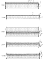
- FIG. 1 is a diagram illustrating a configuration of a SAW device 10 according to the present embodiment.
- the SAW device 10 includes a laminated substrate portion 80, an IDT (Interdigital Transducer) electrode 50, a protective insulating film 70, and a wiring 60.
- the multilayer substrate portion 80 has an overall thickness of about 250 ⁇ m, and includes the piezoelectric single crystal thin film 11, the support substrate 12, the oxide layers 31 and 32, the semiconductive layer 44, and the dielectric layer 21. I have.
- the support substrate 12 is provided on the bottom surface of the multilayer substrate portion 80.
- the support substrate 12 is made of an alumina substrate or a magnesia substrate.
- the alumina substrate and the magnesia substrate are materials having good thermal conductivity and a linear expansion coefficient smaller than that of the piezoelectric single crystal material.
- the SAW device 10 has improved frequency temperature characteristics, heat dissipation, and power durability.
- the oxide layer 32 is laminated on the upper surface of the support substrate 12.
- the oxide layer 32 is provided for forming the semiconductive layer 44, as will be described in detail later.
- the oxide layer 32 is made of a silicon oxide film.
- the semiconductive layer 44 is formed by being laminated on the upper surface of the oxide layer 32.
- the semiconductive layer 44 is provided in order to diffuse the pyroelectric charge generated in the piezoelectric thin film 11 and prevent local polarization inversion in the piezoelectric thin film 11 and electrode destruction of the IDT electrode 50.
- the semiconductive layer 44 is also used for bonding the piezoelectric thin film 11 and the support substrate 12.
- the semiconductive layer 44 is made of a titanium oxide that is a semiconductor.
- the semiconductive layer 44 is a semiconductor material such as zinc oxide, zirconia oxide, chromium oxide, silicon, or a mixture of titanium and titanium oxide, aluminum And aluminum oxide mixture, cobalt and cobalt oxide mixture, copper and copper oxide mixture, chromium and chromium oxide mixture, iron and iron oxide mixture, molybdenum and molybdenum oxide
- the oxide layer 31 is formed by being laminated on the upper surface of the semiconductive layer 44.
- the oxide layer 31 is provided for forming the semiconductive layer 44 in the same manner as the oxide layer 32 described above.
- the oxide layer 32 is made of a silicon oxide film.
- the dielectric layer 21 is formed by being laminated on the upper surface of the oxide layer 31.
- the dielectric layer 21 is provided for the purpose of performing a function of trapping surface acoustic waves in the SAW device 10 in the surface layer and obtaining good characteristics.
- the dielectric layer 21 used here is a laminated film of a silicon oxide film (not shown) having a thickness of 700 nm and an aluminum nitride film (not shown) having a thickness of 1400 nm.
- the dielectric layer 21 is not an essential component and may not be provided.
- the piezoelectric single crystal thin film 11 is formed by being laminated on the upper surface of the dielectric layer 21.
- the piezoelectric single crystal thin film 11 used here is an LT (lithium tantalate) single crystal thin film.
- the material of the piezoelectric single crystal thin film 11 is a piezoelectric material such as LT, LN (LiNbO 3 ), LBO (Li 2 B 4 O 7 ), langasite (La 3 Ga 5 SiO 14 ), and KN (KNbO 3 ). It is good to select suitably.
- LT and LN tend to generate pyroelectric charges. Therefore, when the piezoelectric single crystal thin film 11 is made of LT or LN, the provision of the semiconductive layer 44 causes a problem that pyroelectric charges are caused. The effect of preventing the occurrence of is increased.
- the IDT electrode 50 and the wiring 60 are patterned on the upper surface of the piezoelectric single crystal thin film 11.
- the IDT electrode 50 is a functional electrode in this embodiment, and is electromechanically coupled to the piezoelectric single crystal thin film 11 and constitutes a surface acoustic wave element together with the piezoelectric single crystal thin film 11.
- the wiring 60 transmits a high frequency signal between the IDT electrode 50 and an external circuit.
- the IDT electrode 50 and the wiring 60 used here are a laminated film of aluminum and titanium. Note that the aluminum film may be formed using an alloy mainly containing aluminum, such as an Al—Cu alloy.
- the coercive electric field of the piezoelectric single crystal thin film 11 (here, the LT single crystal having a thickness of 500 nm) is approximately 20 to 30 kV / mm. Therefore, when the polarization axis of the piezoelectric single crystal thin film 11 is in the normal direction of the main surface of the piezoelectric single crystal thin film 11, an electric field due to a voltage of 10 to 15 V is generated between both main surfaces of the piezoelectric single crystal thin film 11. In this case, polarization inversion occurs beyond the coercive electric field of the piezoelectric single crystal thin film 11.
- the polarization axis of the piezoelectric single crystal thin film 11 When the polarization axis of the piezoelectric single crystal thin film 11 is tilted from the normal direction of the main surface of the piezoelectric single crystal thin film 11, the electric field leading to polarization inversion becomes large, and the polarization axis is the main axis of the piezoelectric single crystal thin film 11.
- the surface When the surface is inclined by 45 ° from the surface normal direction, an electric field with a voltage of 14.1 to 21.2 V is required.
- the pyroelectric charge generated in the piezoelectric single crystal thin film 11 is not diffused in the semiconductive layer 44, a voltage of several tens of volts is a voltage level at which polarization inversion can be easily realized. Therefore, the electric charge generated in the piezoelectric single crystal thin film 11 is diffused by the semiconductive layer 44, thereby preventing concentration of the electric field due to the electric charge and avoiding the generation of the domain-inverted region and the destruction of the IDT electrode 50. Can do. Specifically, when the thickness of the semiconductive layer 44 is in the range of 0.1 to 100 nm and the resistivity is 1 ⁇ 10 2 ( ⁇ ⁇ m) or less, polarization inversion occurs in the piezoelectric single crystal thin film 11. Is almost gone. This is shown below.
- the resistivity is 1 ⁇ 10 ⁇ 5 when the thickness of the semiconductive layer 44 is in the range of 0.1 to 100 nm. If it is ( ⁇ ⁇ m) or more, the deterioration of the device characteristics (impedance ratio) can be suppressed to several percent or less.
- the semiconductive layer 44 having a layer thickness of 1 nm and a volume resistivity of 1 ⁇ 10 ⁇ 5 ( ⁇ ⁇ m) to 1 ⁇ 10 2 ( ⁇ ⁇ m) is bonded to the piezoelectric thin film 11, the support substrate 12, and the like. By disposing between them, the polarization inversion of the piezoelectric thin film 11 due to the pyroelectric charge can be suppressed without causing deterioration of the device characteristics.
- the oxide layer 31 and the dielectric layer 21 are interposed between the piezoelectric single crystal thin film 11 and the semiconductive layer 44.
- Insulating layers such as the oxide layer 31 and the dielectric layer 21 reduce the discharge rate of the pyroelectric charge between the piezoelectric single crystal thin film 11 and the semiconductive layer 44 and reduce the effect of suppressing polarization reversal.
- these insulating layers are extremely thin, such as several ⁇ m or less, they hardly disturb the diffusion of the pyroelectric charge.
- the thickness of the aluminum nitride (insulator) is up to 2000 nm (200 k ⁇ in terms of resistance), a sufficient suppressing effect was observed. Moreover, even if the thickness was up to 5000 nm (500 k ⁇ in terms of resistance), the effect was reduced, but the effect of suppressing polarization inversion was seen compared to the case where there was no semiconductive layer. On the other hand, almost no effect was observed at 10,000 nm (1000 k ⁇ ) or more. Therefore, it can be seen that the effect of suppressing the adverse effect of the pyroelectric charge of the structure of the present invention is maintained if the insulator layer has a certain thickness.
- the generation of pyroelectric charge may be prevented by lowering the resistivity of the piezoelectric body itself. In that case, it is necessary to prevent the resistivity from increasing due to oxidation of the piezoelectric body, and it is necessary to accommodate the piezoelectric device in the internal space of the hermetic package in which the inert gas is sealed. Therefore, conventionally, not only is the package cost high, but it is difficult to reduce the height of the package.
- the piezoelectric device having the configuration shown in this embodiment the pyroelectric charge can be reliably diffused by the semiconductive layer 44 regardless of the resistivity of the piezoelectric body. For this reason, there is no need to accommodate the piezoelectric device in an airtight package filled with an inert gas, the package cost can be reduced, and the package can be easily reduced in height.
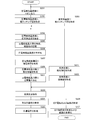
- FIG. 2 is a diagram for explaining the manufacturing flow of the SAW device of this embodiment.
- 3 to 4 are schematic diagrams in each process of the manufacturing flow.
- the piezoelectric single crystal substrate 1 is prepared, and then ions are implanted from the main surface 1A (bonding surface 1A) side of the piezoelectric single crystal substrate 1 in order to separate the piezoelectric single crystal thin film 11 (not shown) (S101). ).
- This step corresponds to the ion implantation step in this embodiment.
- the defect layer 2 is formed at a predetermined depth from the bonding surface 1A of the piezoelectric single crystal substrate 1.
- the defect layer 2 is a region where atoms of ions implanted into the piezoelectric single crystal substrate 1 are concentrated.
- the ions used here are hydrogen ions.
- hydrogen ions are implanted into the piezoelectric single crystal substrate 1 at an acceleration voltage of 80 KeV and a dose of 1.0 ⁇ 10 17 atoms / cm 2 .
- the defect layer 2 is formed at a depth of about 550 nm from the bonding surface 1A.
- the formation position of the defect layer 2 is determined by the acceleration voltage at the time of ion implantation. For example, when the defect layer 2 is formed at about half the depth, the acceleration voltage may be about halved.
- ions to be implanted may be appropriately selected from hydrogen ions, helium ions, argon ions, and the like.
- a dielectric layer 21 is formed on the bonding surface 1A of the piezoelectric single crystal substrate 1 (S102).
- an oxide layer 31 made of silicon oxide is formed on the surface of the dielectric layer 21 (S103).
- the surface of the oxide layer 31 is preferably planarized by a CMP (Chemical Mechanical Polishing) method or the like.
- the oxide layer 31 may be made of a material other than silicon oxide as long as it becomes an oxygen supply source to the metal bonding layer 43 (not shown) later.
- the film thickness may be appropriately adjusted according to the type and film thickness of the metal bonding layer 43 (not shown).
- the support substrate 12 is prepared, and the oxide layer 32 made of silicon oxide is formed on the surface of the support substrate 12 (S111).
- the surface of the oxide layer 32 is preferably planarized by a CMP method or the like.
- the oxide layer 32 may be made of a material other than silicon oxide as long as it becomes an oxygen supply source to the metal bonding layer 43 (not shown) later, similarly to the oxide layer 31 described above. good.
- the film thickness may be appropriately adjusted according to the type and film thickness of the metal bonding layer 43 (not shown).
- the step of forming the oxide layers 31 and 32 corresponds to the oxide layer forming step in the present embodiment.
- a later metal bonding layer 43 (reference number not shown) is provided. Oxidation (shown) can be performed at a lower temperature and in a shorter time.
- an ultrathin metal layer 41 is formed by sputtering on the surface of the oxide layer 31 on the piezoelectric single crystal substrate 1 side (S121). This step corresponds to the first metal layer forming step in the present embodiment.
- the metal layer 41 used here is a titanium thin film having a thickness of 1 nm or less.
- a very thin metal layer 42 is formed by sputtering on the surface of the oxide layer 32 on the support substrate 12 side (S122). This step corresponds to the second metal layer forming step in the present embodiment.
- the metal layer 42 is also a titanium thin film having a thickness of 1 nm or less.
- the metal layers 41 and 42 may be made of aluminum, cobalt, copper, chromium, iron, molybdenum, nickel, niobium, titanium, silicon, tantalum, tungsten, zinc, zirconium, etc. in addition to titanium.
- a metal layer 42 (reference numeral not shown) on the support substrate 12 side and a metal layer 41 (reference numeral not shown) on the piezoelectric single crystal substrate 1 side are overlapped to form 2 nm.
- a metal bonding layer 43 having the following thickness is formed (S123). This step corresponds to the metal layer bonding step in this embodiment. In addition, the whole process so far is corresponded to the conjugate
- the formation process of the metal layers 41 and 42 and the formation process of the metal bonding layer 43 are continuously performed in a high vacuum of 10 ⁇ 6 Pa or less. Thereby, the metal layers 41 and 42 are firmly bonded to form an integral crystal, and the metal bonding layer 43 is formed.
- the metal layers 41 and 42 constituting the metal bonding layer 43 are preferably the same kind of metal material. This is because, in the case of a dissimilar metal material, a cavity portion may be generated in the bonded metal portion or the bonding strength may be deteriorated due to segregation due to a difference in diffusion rate during heating.
- the metal layers 41 and 42 are preferably made of a metal material having a large diffusion coefficient (diffusion rate). This is because a metal material having a large diffusion coefficient can provide a large margin regarding the flatness of the joint surface.
- the metal layers 41 and 42 are preferably a metal material having a negative free energy of formation of oxides and are easily oxidized.
- the bonded body of the support substrate 12 and the piezoelectric single crystal substrate 1 firmly bonded via the metal bonding layer 43 is placed in a heating environment of about 250 ° C. (S124). Then, as shown in FIG. 4 (S124), the piezoelectric single crystal substrate 1 (not shown) is separated by the defect layer 2 (not shown), and the piezoelectric single crystal thin film 11 is formed. This step corresponds to the separation step in this embodiment.
- the piezoelectric single crystal thin film 11 having an extremely thin film thickness that maintains a good film thickness distribution. It can.
- the crystal orientation of the piezoelectric single crystal substrate 1 can be arbitrarily set, by forming the piezoelectric single crystal thin film 11 using ion implantation into the piezoelectric single crystal substrate 1, the piezoelectric single crystal thin film 1 The crystal orientation of 11 can be arbitrarily set. Thereby, the piezoelectric single crystal thin film 11 having a crystal orientation desirable as the SAW device can be obtained, and the piezoelectric characteristics of the SAW device can be improved.
- the surface of the piezoelectric single crystal thin film 11 is planarized by a CMP method or the like (S125).
- the surface of the piezoelectric single crystal thin film 11 is flattened by shaving it by about 50 nm.
- the metal bonding layer 43 (not shown) is oxidized by heating to form the semiconductive layer 44 (S126).
- This step corresponds to the semiconductive layer forming step in the present embodiment. Since the oxide layers 31 and 32 are in contact with the metal bonding layer 43 (not shown), oxygen used for the oxidation reaction is supplied from the oxide layers 31 and 32.
- the metal bonding layer 43 symbol not shown
- the semiconductive layer 44 is in a state where the semiconductor material is titanium oxide or a mixture of titanium and titanium oxide. Therefore, the semiconductive layer 44 can diffuse the pyroelectric charges without affecting the device characteristics.
- the semiconductive layer 44 since the metal bonding layer 43 is formed by diffusion by heating, the semiconductive layer 44 has a film thickness that is larger than that of the metal bonding layer. Specifically, as described above, the film thickness of the semiconductive layer 44 is in a range up to about 100 nm.
- the heating temperature and heating time in this step may be selected appropriately depending on the material type and thickness of the metal bonding layer 43.
- the metal bonding layer 43 is a titanium thin film having a thickness of 1 nm
- the heating temperature is about 300 ° C. and the heating time is about 1 hour
- the semiconductive layer 44 is sufficiently oxidized to form titanium which is a semiconductor material. It can be an oxide.
- the semiconductive layer 44 is formed by stopping the oxidation of the metal bonding layer 43 in a state where the metal before being completely oxidized remains. can do.
- the oxidation of the semiconductive layer 44 is performed as a heat treatment step different from the separation of the piezoelectric single crystal thin film 11 described above, but the heating temperature and heating time during the separation of the piezoelectric single crystal thin film 11 are adjusted. At the same time, the semiconductive layer 44 may be oxidized. Further, the heat treatment step for oxidizing the semiconductive layer 44 may be performed before the step of planarizing the surface of the piezoelectric single crystal thin film 11.
- the IDT electrode 50 and the wiring pattern 60A necessary for the operation of the SAW device are formed on the surface of the piezoelectric thin film 11. This step corresponds to the functional electrode forming step in the present embodiment.
- the wiring pattern 60A in a two-layer structure, the low resistance wiring 60 is formed, the IDT electrode 50 is covered with the insulating protective film 70, and the SAW device is manufactured.
- the bonding strength between the piezoelectric single crystal substrate 1 and the support substrate 12 develops in a non-heated environment, so that heating to develop the bonding strength is unnecessary, and the piezoelectric single crystal substrate 1 Even if the difference in linear expansion coefficient between the support substrate 12 and the support substrate 12 is large, various problems are unlikely to occur during bonding.
- the piezoelectric single crystal thin film 11 in order to form the piezoelectric single crystal thin film 11 by ion implantation, ions atoms are present in the crystal of the piezoelectric single crystal thin film 11, and the distribution density thereof is the piezoelectric single crystal. Since the crystal thin film 11 is biased in the thickness direction, the piezoelectric single crystal thin film 11 has a film stress.
- the piezoelectric single crystal thin film 11 (piezoelectric single crystal substrate 1) is easily peeled off from the support substrate 12 due to the addition of the film stress and the thermal stress, thereby realizing stable and strong bonding. Difficult to do. Therefore, the method of the present embodiment, in which strong bonding is manifested from the moment of bonding in a non-heated environment, is not affected by thermal stress during bonding, and thus is an extremely effective technique for stably realizing strong bonding. It can be said that there is.
- the conductivity of the metal bonding layer 43 is high, the characteristics of the SAW device will be adversely affected.
- the metal bonding layer 43 a semiconductive material 44 having a low conductivity after bonding, a good SAW can be obtained. Device characteristics will be obtained.
- the pyroelectric charge generated in the piezoelectric single crystal thin film 11 may cause deterioration of piezoelectricity or electrode breakage of the IDT electrode 50.
- the semiconductive material 44 is provided to disperse the pyroelectric charge. Thus, the occurrence of these problems can also be prevented.
- Second Embodiment a method for manufacturing a piezoelectric device according to the second embodiment of the present invention will be described using a method for manufacturing a SAW device as a specific example.
- the piezoelectric single crystal thin film in order to recover the piezoelectricity and crystallinity of the piezoelectric single crystal thin film that is lowered to a certain extent by ion implantation, the piezoelectric single crystal thin film is subjected to high-temperature heat treatment at about 500 ° C.
- high-temperature heat treatment at about 500 ° C.
- FIG. 6 is a diagram for explaining the manufacturing flow of the SAW device of this embodiment.
- 7 and 8 are schematic diagrams in each step of the first half of the manufacturing flow.
- a piezoelectric single crystal substrate 201 is prepared, and ions are implanted from the main surface 201A (joint surface 1A) side of the piezoelectric single crystal substrate 201.
- the defect layer 202 is formed at a predetermined depth from the bonding surface 201A of the piezoelectric single crystal substrate 201.
- an etching target layer 291 is formed on the bonding surface 201A of the piezoelectric single crystal substrate 201.
- the surface of the etching target layer 291 is preferably planarized by a CMP method or the like. This etched layer 291 is to be removed later by etching.
- the layer to be etched 291 used here is a Cu film having a thickness of 3 ⁇ m.
- a temporary support substrate 212 is prepared, and an etched layer 292 is also formed on the surface of the temporary support substrate 212.
- the surface of the etching target layer 292 is preferably planarized by a CMP method or the like.
- the temporary support substrate 212 used here is the same material as the piezoelectric single crystal substrate 201. Since the piezoelectric single crystal thin film 211 (symbol not shown) is later subjected to high-temperature heat treatment while being bonded to such a temporary support substrate, it is possible to prevent the wafer from being cracked due to the heat treatment.
- the material of the temporary support substrate 212 may be another material that has a small difference in linear expansion coefficient from the piezoelectric single crystal thin film 211 (not shown).
- the layer to be etched 292 used here is a Cu film having a thickness of 3 ⁇ m.
- the to-be-etched layer 292 (reference numeral not shown) and the to-be-etched layer 291 (reference numeral not shown) are joined to form the to-be-etched joining layer 293.
- the joining method here may be a joining method that provides a certain degree of joining strength. Since the temporary support substrate 212 and the piezoelectric single crystal substrate 201 have the same linear expansion coefficient, a bonding method that requires heating may be used.
- the bonded body of the temporary support substrate 212 and the piezoelectric single crystal substrate 201 bonded through the bonding layer 293 to be etched is placed in a heating environment of about 250 ° C.
- the piezoelectric single crystal substrate 201 (not shown) is separated by the defect layer 202 (not shown) to form the piezoelectric single crystal thin film 211.
- the bonded body of the temporary support substrate 212 and the piezoelectric single crystal thin film 211 bonded through the bonding layer 293 to be etched is placed in a high temperature environment of about 500 ° C.
- the crystallinity of the piezoelectric single crystal thin film 211 broken by the ion implantation is recovered. Since the temporary support substrate 212 and the piezoelectric single crystal substrate 201 (not shown) have the same material and the same linear expansion coefficient, deformation due to these heat treatments hardly occurs, and the piezoelectric single crystal substrate 201 is not destroyed. It is prevented.
- the surface of the piezoelectric single crystal thin film 211 is planarized by a CMP method or the like.
- the thin film temporary support structure 200 in which the piezoelectric single crystal thin film 211 is bonded to the temporary support substrate 212 through the bonding layer 293 to be etched is configured.
- a dielectric layer 221 is formed on the surface of the piezoelectric single crystal thin film 211 in the thin film temporary support structure 200.
- an oxide layer 231 is formed on the surface of the dielectric layer 221 in the thin film temporary support structure 200.
- a support substrate 213 is prepared, and an oxide layer 233 is formed on the surface of the support substrate 213.
- a very thin metal layer 241 is formed on the surface of the oxide layer 231 in the thin film temporary support structure 200.
- an extremely thin metal layer 243 is formed on the surface of the oxide layer 233 on the support substrate 213 side.
- the metal layer 243 (reference numeral not shown) on the support substrate 213 side and the metal layer 241 (reference numeral not shown) on the thin film temporary support structure 200 side are overlapped to perform metal bonding.
- Layer 244 is formed.
- the formation process of the above-mentioned metal layers 241 and 243 and this joining process are continuously performed in a high vacuum, and joining between the metal layers 241 and 243 is implement
- the bonded body obtained by bonding the piezoelectric single crystal thin film 211, the temporary support substrate 212, and the support substrate 213 is dipped in an etching solution such as nitric acid, and the bonding layer 293 to be etched is etched.
- the temporary support substrate 212 is removed.
- a structure in which the piezoelectric single crystal thin film 211 and the support substrate 213 are bonded via the metal bonding layer 244 as shown in FIG. 8 (S224) is configured.
- a semiconductive layer (not shown) is formed by oxidation of the metal bonding layer 244, and an IDT electrode and an insulating protective film are formed.
- the SAW device is manufactured (S225 ⁇ S226 ⁇ S227).
- the piezoelectric device according to the present invention is made of a piezoelectric single crystal material, it can be manufactured while suppressing problems.
- the support substrate itself is formed on the piezoelectric thin film after heating, it is not necessary to consider the thermal stress acting on the interface with the piezoelectric thin film due to heating, and a constituent material having an arbitrary linear expansion coefficient can be selected. Therefore, the selectivity of the combination of the constituent material of the piezoelectric thin film and the constituent material of the support substrate can be enhanced.
- the temperature-frequency characteristics of the filter can be improved by making the linear expansion coefficient of the constituent material of the support substrate much smaller than the linear expansion coefficient of the piezoelectric thin film.
- the piezoelectric single crystal thin film 311 as shown in FIG. 10 (S301) is bonded to the temporary support substrate 312 via the bonding target layer 393 by the same method as in the second embodiment.
- a thin film temporary support structure 300 is formed.
- a lower electrode pattern 321 for driving the BAW device is formed on the surface of the piezoelectric single crystal thin film 311 in the thin film temporary support structure 300.
- a sacrificial layer pattern for forming a cavity portion of the membrane structure on the surface of the piezoelectric single crystal thin film 311 in the thin film temporary support structure 300 so as to cover the lower electrode pattern 321. 331 is formed.
- a membrane support layer 341 is formed on the surface of the piezoelectric single crystal thin film 311 in the thin film temporary support structure 300 so as to cover the sacrificial layer pattern 331.
- the surface of the membrane support layer 341 is planarized by CMP after sputter deposition.
- the membrane support layer 341 used here is a silicon oxide film and is used later as an oxide layer.
- a support substrate 313 is prepared, and an oxide layer 343 is formed on the surface of the support substrate 313.
- a very thin metal layer 351 is formed on the surface of the membrane support layer 341 in the thin film temporary support structure 300.
- an extremely thin metal layer 353 is formed on the surface of the oxide layer 343 on the support substrate 313 side.
- a metal layer 353 (reference numeral not shown) on the support substrate 313 side and a metal layer 351 (reference numeral not shown) on the thin film temporary support structure 300 side are overlapped to form a metal.
- a bonding layer 354 is formed.
- the formation process of the above-mentioned metal layer 351,353 and this joining process are continuously implemented in a high vacuum, and joining between the metal layers 351,353 is implement
- the bonded body obtained by bonding the piezoelectric single crystal thin film 311, the temporary support substrate 312, and the support substrate 313 is dipped in an etching solution such as nitric acid, the etched bonding layer 393 is etched, and the etched bonding layer 393 and The temporary support substrate 312 is removed.
- an etching solution such as nitric acid
- the etched bonding layer 393 is etched
- the etched bonding layer 393 and The temporary support substrate 312 is removed.
- the metal bonding layer 354 (not shown) is oxidized by heating to form a semiconductive layer 355.
- the piezoelectric single crystal thin film 311 is subjected to a window opening process and an upper electrode pattern for driving the BAW device is formed.
- an etchant is introduced into the sacrificial layer pattern 331 (not shown) from the window of the piezoelectric single crystal thin film 311, and the sacrificial layer pattern 331 (not shown) is removed to remove the membrane.
- a space 331A is formed.
- the BAW device is manufactured by dividing into individual pieces.
- the piezoelectric device of the present invention can be manufactured by the manufacturing method shown in the above embodiments, the piezoelectric device may be manufactured by other methods.
- the formation of the piezoelectric single crystal thin film can be realized by ion implantation and separation into the piezoelectric single crystal substrate, or by sputtering film formation, grinding of the piezoelectric single crystal substrate, etching of the piezoelectric single crystal substrate, or the like.
- the formation of the semiconductive layer may be realized by thermal oxidation of the metal layer, or may be realized by sputtering a semiconductor material or bonding a member to be the semiconductive layer to another member.
- the piezoelectric device the SAW device and the BAW device are shown in the present embodiment, but the present invention is not limited to this, and a boundary acoustic wave device in which an insulating layer is provided so as to cover the IDT electrode, and other plate waves It can also be applied to devices and Lamb wave devices.
Landscapes
- Engineering & Computer Science (AREA)
- Manufacturing & Machinery (AREA)
- Physics & Mathematics (AREA)
- Acoustics & Sound (AREA)
- Surface Acoustic Wave Elements And Circuit Networks Thereof (AREA)
Abstract
Description
なお、上述の圧電デバイスにおいて、半導電層の体積抵抗率は、1×10⁻⁵(Ω・m)~1×10²(Ω・m)であると好適である。
また、上述の圧電デバイスにおいて、半導電層は、半導体材料であるチタン酸化物、亜鉛酸化物、ジルコニア酸化物、クロム酸化物、シリコンのいずれか、または、アルミニウムとアルミニウム酸化物との混合物、コバルトとコバルト酸化物との混合物、銅と銅酸化物との混合物、クロムとクロム酸化物との混合物、鉄と鉄酸化物との混合物、モリブデンとモリブデン酸化物との混合物、ニッケルとニッケル酸化物との混合物、ニオブとニオブ酸化物との混合物、チタンとチタン酸化物との混合物、シリコンとシリコン酸化物との混合物、タンタルとタンタル酸化物との混合物、タングステンとタングステン酸化物との混合物、亜鉛と亜鉛酸化物との混合物、ジルコニウムとジルコニウム酸化物との混合物、のいずれかであると好適である。
また、上述の圧電デバイスにおいて、半導電層は、膜厚が100nm以下であると好適である。 In this configuration, the pyroelectric charge generated when heat is applied diffuses through the semiconductive layer, and the electric field due to the pyroelectric charge is not locally increased in the piezoelectric thin film. Thereby, it is possible to prevent the electric field due to the pyroelectric charge from exceeding the coercive electric field of the piezoelectric thin film, and to prevent the occurrence of polarization inversion in the piezoelectric thin film and the electrode destruction of the functional electrode. In addition, by providing the semiconductive layer, it is not necessary to provide an unnecessary electrode structure, and deterioration of electrical characteristics (device characteristics) due to leakage of electrical signals can be prevented.
In the above-described piezoelectric device, the volume resistivity of the semiconductive layer is preferably 1 × 10 −5 (Ω · m) to 1 × 10 2 (Ω · m).
Further, in the above-described piezoelectric device, the semiconductive layer is formed of a semiconductor material such as titanium oxide, zinc oxide, zirconia oxide, chromium oxide, silicon, a mixture of aluminum and aluminum oxide, cobalt And a mixture of cobalt oxide, a mixture of copper and copper oxide, a mixture of chromium and chromium oxide, a mixture of iron and iron oxide, a mixture of molybdenum and molybdenum oxide, nickel and nickel oxide A mixture of niobium and niobium oxide, a mixture of titanium and titanium oxide, a mixture of silicon and silicon oxide, a mixture of tantalum and tantalum oxide, a mixture of tungsten and tungsten oxide, and zinc It is preferable that it is either a mixture with zinc oxide or a mixture of zirconium and zirconium oxide.
In the above-described piezoelectric device, the semiconductive layer preferably has a thickness of 100 nm or less.
また、上述の圧電デバイスにおいて、圧電体単結晶薄膜は、水素原子またはヘリウム原子が介在原子として結晶に介在し、第一主面側と第二主面側とで介在原子の分布密度に差がある構造であってもよい。 In the above-described piezoelectric device, the piezoelectric thin film is made of a piezoelectric single crystal, and the piezoelectric single crystal thin film may have a difference in film stress between the first main surface side and the second main surface side.
In the piezoelectric device described above, the piezoelectric single crystal thin film has hydrogen atoms or helium atoms intervening in the crystal as intervening atoms, and there is a difference in the distribution density of intervening atoms between the first main surface side and the second main surface side. It may be a certain structure.
この製造方法では、酸化物層が金属層の酸化反応に対する酸素供給源となって、金属層の酸化に要する時間や、加熱により酸化させる場合の加熱温度を大幅に低減することができる。 The above-described method for manufacturing a piezoelectric device preferably includes an oxide layer forming step of forming an oxide layer stacked on the metal layer.
In this manufacturing method, the oxide layer serves as an oxygen supply source for the oxidation reaction of the metal layer, and the time required for the oxidation of the metal layer and the heating temperature when oxidizing by heating can be greatly reduced.
また、仮支持工程と、支持工程と、をさらに有すると好適である。仮支持工程は、圧電基板のイオン注入面側に、圧電基板と同種の材料からなる、あるいは、圧電基板との界面に作用する熱応力が支持基板と圧電基板との界面に作用する熱応力よりも小さい、仮支持基板を形成する工程である。支持工程は、圧電基板から分離した圧電体薄膜に支持基板を形成する工程である。 The above-described method for manufacturing a piezoelectric device preferably includes an ion implantation step and a separation step. The ion implantation step is a step of implanting ionized elements from the bonding surface of the piezoelectric substrate to form a region where the elements are concentrated in the piezoelectric substrate. The separation step is a step of separating the region on the bonding surface side of the piezoelectric substrate as a piezoelectric thin film by heating.
Moreover, it is suitable to further have a temporary support process and a support process. In the temporary support process, the thermal stress acting on the interface between the support substrate and the piezoelectric substrate is made of the same kind of material as the piezoelectric substrate on the ion implantation surface side of the piezoelectric substrate, or the thermal stress acting on the interface between the support substrate and the piezoelectric substrate. Is a step of forming a temporary support substrate. The supporting step is a step of forming the supporting substrate on the piezoelectric thin film separated from the piezoelectric substrate.
まず、本発明の第1の実施形態に係る圧電デバイスについて、SAW(SurfaceAcoustic Wave;弾性表面波)デバイスを具体例として説明する。
図1は、本実施形態のSAWデバイス10の構成を示す図である。 << First Embodiment >>
First, the piezoelectric device according to the first embodiment of the present invention will be described using a SAW (Surface Acoustic Wave) device as a specific example.
FIG. 1 is a diagram illustrating a configuration of a SAW device 10 according to the present embodiment.


図3~4は、製造フローの各工程における模式図である。 FIG. 2 is a diagram for explaining the manufacturing flow of the SAW device of this embodiment.
3 to 4 are schematic diagrams in each process of the manufacturing flow.
次に、本発明の第2の実施形態に係る圧電デバイスの製造方法について、SAWデバイスの製造方法を具体例として説明する。 << Second Embodiment >>
Next, a method for manufacturing a piezoelectric device according to the second embodiment of the present invention will be described using a method for manufacturing a SAW device as a specific example.
図7,8は、製造フローの前半の各工程における模式図である。 FIG. 6 is a diagram for explaining the manufacturing flow of the SAW device of this embodiment.
7 and 8 are schematic diagrams in each step of the first half of the manufacturing flow.
したがって、圧電薄膜の構成材料と支持基板の構成材料との組み合わせの選択性を高められる。例えば、フィルタ用途のデバイスでは、支持基板の構成材料の線膨張係数を圧電薄膜の線膨張係数よりも大幅に小さくすることで、フィルタの温度-周波数特性を向上させることが可能になる。また、支持基板に熱伝導率性が高い構成材料を選定して放熱性および耐電力性を向上させることが可能になり、安価な構成材料を選定してデバイスの製造コストを低廉にすることが可能になる。 In the second embodiment, there is almost no thermal stress that acts on the interface with the piezoelectric substrate, or thermal stress that acts on the interface with the piezoelectric substrate acts on the interface between the support substrate and the piezoelectric substrate. Since the smaller temporary support substrate is formed on the ion-implanted surface side of the piezoelectric substrate, it is possible to suppress the occurrence of defects of the piezoelectric thin film due to heating as compared with the conventional case. In addition, when the piezoelectric device according to the present invention is made of a piezoelectric single crystal material, it can be manufactured while suppressing problems. Since the support substrate itself is formed on the piezoelectric thin film after heating, it is not necessary to consider the thermal stress acting on the interface with the piezoelectric thin film due to heating, and a constituent material having an arbitrary linear expansion coefficient can be selected.
Therefore, the selectivity of the combination of the constituent material of the piezoelectric thin film and the constituent material of the support substrate can be enhanced. For example, in a filter device, the temperature-frequency characteristics of the filter can be improved by making the linear expansion coefficient of the constituent material of the support substrate much smaller than the linear expansion coefficient of the piezoelectric thin film. In addition, it is possible to improve the heat dissipation and power durability by selecting a constituent material with high thermal conductivity for the support substrate, and to select a cheap constituent material to reduce the manufacturing cost of the device. It becomes possible.
次に、本発明の第3の実施形態に係る圧電デバイスについて、圧電単結晶薄膜をメンブレン構造で支持するBAW(Bulk Acoustic Wave;バルク弾性波)デバイスの製造方法を具体例として説明する。 << Third Embodiment >>
Next, regarding a piezoelectric device according to the third embodiment of the present invention, a method for manufacturing a BAW (Bulk Acoustic Wave) device that supports a piezoelectric single crystal thin film with a membrane structure will be described as a specific example.
また、圧電デバイスとして、本実施形態ではSAWデバイスとBAWデバイスについて示したが、これに限られるものではなく、IDT電極を覆うように絶縁層が設けられた弾性境界波デバイスや、その他、板波デバイス、ラム波デバイスなどにも適用できる。 Although the piezoelectric device of the present invention can be manufactured by the manufacturing method shown in the above embodiments, the piezoelectric device may be manufactured by other methods. For example, the formation of the piezoelectric single crystal thin film can be realized by ion implantation and separation into the piezoelectric single crystal substrate, or by sputtering film formation, grinding of the piezoelectric single crystal substrate, etching of the piezoelectric single crystal substrate, or the like. Good. Further, the formation of the semiconductive layer may be realized by thermal oxidation of the metal layer, or may be realized by sputtering a semiconductor material or bonding a member to be the semiconductive layer to another member.
In addition, as the piezoelectric device, the SAW device and the BAW device are shown in the present embodiment, but the present invention is not limited to this, and a boundary acoustic wave device in which an insulating layer is provided so as to cover the IDT electrode, and other plate waves It can also be applied to devices and Lamb wave devices.
1A,201A…接合面
2,202…欠陥層
10…SAWデバイス
11,211,311…圧電体薄膜
12,213,313…支持基板
21,221…誘電体層
31,32,231,233,343…酸化物層
41,42,241,243,351,353…金属層
43,244,354…金属接合層
44,355…半導電層
50…IDT電極
60A…配線パターン
60B…2層配線部
70…絶縁性保護膜
200,300…薄膜仮支持構造
212,312…仮支持基板
291…被エッチング層
292…被エッチング層
293,393…被エッチング接合層
321…下部電極パターン
331…犠牲層パターン
331A…メンブレン空間
341…メンブレン支持層 DESCRIPTION OF SYMBOLS 1,201 ... Piezoelectric
Claims (11)
- 圧電体薄膜と、
前記圧電体薄膜の第一主面側に設けられて前記圧電体薄膜に電気機械結合する機能電極と、
半導体材料または、金属とその金属の酸化物との混合材料からなり、前記圧電体薄膜の第二主面側に設けられる半導電層と、
前記半導電層を間に介して前記圧電体薄膜の第二主面側に設けられる支持基板と、
を備える圧電デバイス。 A piezoelectric thin film;
A functional electrode provided on the first main surface side of the piezoelectric thin film and electromechanically coupled to the piezoelectric thin film;
A semiconductive layer made of a semiconductor material or a mixed material of a metal and an oxide of the metal, and provided on the second main surface side of the piezoelectric thin film,
A support substrate provided on the second main surface side of the piezoelectric thin film with the semiconductive layer interposed therebetween;
A piezoelectric device comprising: - 前記半導電層の体積抵抗率は、1×10⁻⁵(Ω・m)~1×10²(Ω・m)である、請求項1に記載の圧電デバイス。 2. The piezoelectric device according to claim 1, wherein the volume resistivity of the semiconductive layer is 1 × 10 −5 (Ω · m) to 1 × 10 2 (Ω · m).
- 前記半導電層は、半導体材料であるチタン酸化物、亜鉛酸化物、ジルコニア酸化物、クロム酸化物、シリコンのいずれか、または、アルミニウムとアルミニウム酸化物との混合物、コバルトとコバルト酸化物との混合物、銅と銅酸化物との混合物、クロムとクロム酸化物との混合物、鉄と鉄酸化物との混合物、モリブデンとモリブデン酸化物との混合物、ニッケルとニッケル酸化物との混合物、ニオブとニオブ酸化物との混合物、チタンとチタン酸化物との混合物、シリコンとシリコン酸化物との混合物、タンタルとタンタル酸化物との混合物、タングステンとタングステン酸化物との混合物、亜鉛と亜鉛酸化物との混合物、ジルコニウムとジルコニウム酸化物との混合物、のいずれかである、請求項1又は2に記載の圧電デバイス。 The semiconductive layer is a semiconductor material such as titanium oxide, zinc oxide, zirconia oxide, chromium oxide, silicon, a mixture of aluminum and aluminum oxide, a mixture of cobalt and cobalt oxide. , Mixture of copper and copper oxide, mixture of chromium and chromium oxide, mixture of iron and iron oxide, mixture of molybdenum and molybdenum oxide, mixture of nickel and nickel oxide, niobium and niobium oxidation A mixture of materials, a mixture of titanium and titanium oxide, a mixture of silicon and silicon oxide, a mixture of tantalum and tantalum oxide, a mixture of tungsten and tungsten oxide, a mixture of zinc and zinc oxide, The piezoelectric device according to claim 1, wherein the piezoelectric device is any one of a mixture of zirconium and zirconium oxide.
- 前記半導電層は、膜厚が100nm以下である、請求項1~3のいずれか1項に記載の弾性波デバイスの製造方法。 4. The method for manufacturing an acoustic wave device according to claim 1, wherein the semiconductive layer has a thickness of 100 nm or less.
- 前記圧電体薄膜は圧電単結晶からなり、第一主面側と第二主面側とで膜応力に差がある結晶構造である、請求項1~4のいずれか1項に記載の圧電デバイス。 The piezoelectric device according to any one of claims 1 to 4, wherein the piezoelectric thin film is made of a piezoelectric single crystal and has a crystal structure having a difference in film stress between the first main surface side and the second main surface side. .
- 前記圧電単結晶からなる圧電体薄膜は、水素原子またはヘリウム原子が介在原子として結晶に介在し、第一主面側と第二主面側とで介在原子の分布密度に差がある結晶構造である、請求項5に記載の圧電デバイス。 The piezoelectric thin film made of the piezoelectric single crystal has a crystal structure in which hydrogen atoms or helium atoms are interposed in the crystal as intervening atoms, and the distribution density of intervening atoms is different between the first main surface side and the second main surface side. The piezoelectric device according to claim 5.
- 金属層を間に介した圧電体薄膜と支持基板との接合体を形成する接合体形成工程と、
前記金属層を酸化させて半導電層を形成する半導電層形成工程と、
前記圧電体薄膜の第一主面側に、前記圧電体薄膜に電気機械結合する機能電極を形成する機能電極形成工程と、を有し、
前記半導電層は、前記金属層を構成する金属とその酸化物とが混合する層、または、前記金属層を構成する金属の酸化物である半導体からなる層である、圧電デバイスの製造方法。 A joined body forming step of forming a joined body of the piezoelectric thin film and the support substrate with the metal layer interposed therebetween;
A semiconductive layer forming step of oxidizing the metal layer to form a semiconductive layer;
Forming a functional electrode that is electromechanically coupled to the piezoelectric thin film on the first main surface side of the piezoelectric thin film; and
The method for manufacturing a piezoelectric device, wherein the semiconductive layer is a layer in which a metal constituting the metal layer and an oxide thereof are mixed, or a layer made of a semiconductor which is an oxide of the metal constituting the metal layer. - 前記金属層に積層される、酸化物層を形成する酸化物層形成工程を、有する、請求項7に記載の圧電デバイスの製造方法。 The method for manufacturing a piezoelectric device according to claim 7, further comprising an oxide layer forming step of forming an oxide layer laminated on the metal layer.
- 前記接合体形成工程は、不活性ガス雰囲気下または真空下で連続して行われる、請求項7または8に記載の圧電デバイスの製造方法。 The method for manufacturing a piezoelectric device according to claim 7 or 8, wherein the joined body forming step is continuously performed in an inert gas atmosphere or in a vacuum.
- 圧電基板の接合面からイオン化した元素を注入して、前記圧電基板の中に前記元素が集中して存在する領域を形成するイオン注入工程と、
加熱により前記圧電基板における接合面側の領域を圧電体薄膜として残す分離工程と、を有する請求項7~9のいずれか1項に記載の圧電デバイスの製造方法。 An ion implantation step of injecting an ionized element from the bonding surface of the piezoelectric substrate to form a region in which the element is concentrated in the piezoelectric substrate;
The method for manufacturing a piezoelectric device according to any one of claims 7 to 9, further comprising a separation step of leaving a region on the bonding surface side of the piezoelectric substrate as a piezoelectric thin film by heating. - 圧電基板にイオン化した元素を注入して、前記圧電基板の中に前記元素が集中して存在する領域を形成するイオン注入工程と、
前記圧電基板のイオン注入面側に、前記圧電基板と同種の材料からなる、あるいは、前記圧電基板との界面に作用する熱応力が前記支持基板と前記圧電基板との界面に作用する熱応力よりも小さい、仮支持基板を形成する仮支持工程と、
加熱により前記圧電基板から圧電体薄膜を分離する分離工程と、
前記圧電基板から分離した前記圧電体薄膜に前記支持基板を形成する支持工程と、
を有する請求項7~9のいずれか1項に記載の圧電デバイスの製造方法。 An ion implantation step of implanting ionized elements into the piezoelectric substrate to form a region where the elements are concentrated in the piezoelectric substrate;
From the thermal stress acting on the interface between the support substrate and the piezoelectric substrate, the thermal stress acting on the interface with the piezoelectric substrate is made of the same kind of material as the piezoelectric substrate on the ion implantation surface side of the piezoelectric substrate. A temporary support step for forming a temporary support substrate,
A separation step of separating the piezoelectric thin film from the piezoelectric substrate by heating;
A support step of forming the support substrate on the piezoelectric thin film separated from the piezoelectric substrate;
The method for manufacturing a piezoelectric device according to any one of claims 7 to 9, wherein:
Priority Applications (6)
| Application Number | Priority Date | Filing Date | Title |
|---|---|---|---|
| JP2013526837A JP5835329B2 (en) | 2011-07-29 | 2012-07-25 | Piezoelectric device and method for manufacturing piezoelectric device |
| CN201280038231.0A CN103718457B (en) | 2011-07-29 | 2012-07-25 | Piezoelectric device and method of manufacturing piezoelectric device |
| KR1020147002046A KR101635151B1 (en) | 2011-07-29 | 2012-07-25 | Piezoelectric device and method of manufacturing piezoelectric device |
| EP12820240.5A EP2738939B1 (en) | 2011-07-29 | 2012-07-25 | Piezoelectric device and method of manufacturing piezoelectric device |
| US14/164,318 US9577178B2 (en) | 2011-07-29 | 2014-01-27 | Piezoelectric device and method for producing piezoelectric device |
| US15/379,530 US10424716B2 (en) | 2011-07-29 | 2016-12-15 | Method for producing piezoelectric device |
Applications Claiming Priority (2)
| Application Number | Priority Date | Filing Date | Title |
|---|---|---|---|
| JP2011-166586 | 2011-07-29 | ||
| JP2011166586 | 2011-07-29 |
Related Child Applications (1)
| Application Number | Title | Priority Date | Filing Date |
|---|---|---|---|
| US14/164,318 Continuation US9577178B2 (en) | 2011-07-29 | 2014-01-27 | Piezoelectric device and method for producing piezoelectric device |
Publications (1)
| Publication Number | Publication Date |
|---|---|
| WO2013018604A1 true WO2013018604A1 (en) | 2013-02-07 |
Family
ID=47629130
Family Applications (1)
| Application Number | Title | Priority Date | Filing Date |
|---|---|---|---|
| PCT/JP2012/068788 WO2013018604A1 (en) | 2011-07-29 | 2012-07-25 | Piezoelectric device and method of manufacturing piezoelectric device |
Country Status (6)
| Country | Link |
|---|---|
| US (2) | US9577178B2 (en) |
| EP (1) | EP2738939B1 (en) |
| JP (1) | JP5835329B2 (en) |
| KR (1) | KR101635151B1 (en) |
| CN (1) | CN103718457B (en) |
| WO (1) | WO2013018604A1 (en) |
Cited By (8)
| Publication number | Priority date | Publication date | Assignee | Title |
|---|---|---|---|---|
| WO2015186661A1 (en) * | 2014-06-04 | 2015-12-10 | 株式会社村田製作所 | Elastic wave device |
| CN106291142A (en) * | 2016-09-19 | 2017-01-04 | 郑州大学 | Piezoelectric ceramics and piezoelectric semiconductor's test specimen multiformity polarization experiment system |
| CN107192897A (en) * | 2017-07-14 | 2017-09-22 | 郑州大学 | A kind of piezoelectric semiconductor's membrane polarization experimental provision |
| JP2019506043A (en) * | 2015-12-22 | 2019-02-28 | ソワテク | Substrates for temperature compensated surface acoustic wave devices or bulk acoustic wave devices |
| JP2020145530A (en) * | 2019-03-05 | 2020-09-10 | 京セラ株式会社 | Elastic wave device |
| JP2021048624A (en) * | 2015-12-22 | 2021-03-25 | ソワテク | Method for manufacturing monocrystalline piezoelectric layer, and microelectronic, photonic or optical device including such layer |
| US20210211114A1 (en) * | 2020-01-03 | 2021-07-08 | Wisol Co., Ltd. | Surface acoustic wave device and manufacturing method thereof |
| JP2021158511A (en) * | 2020-03-26 | 2021-10-07 | 太陽誘電株式会社 | Piezoelectric thin film resonator, filter, and multiplexer |
Families Citing this family (22)
| Publication number | Priority date | Publication date | Assignee | Title |
|---|---|---|---|---|
| JP4582235B2 (en) * | 2008-10-31 | 2010-11-17 | 株式会社村田製作所 | Method for manufacturing piezoelectric device |
| JP5842911B2 (en) * | 2011-03-14 | 2016-01-13 | 株式会社村田製作所 | Piezoelectric device and method for manufacturing piezoelectric device |
| KR102480632B1 (en) | 2015-03-23 | 2022-12-26 | 삼성디스플레이 주식회사 | Piezoelectric device and piezoelectric sensor using the same |
| FR3037443B1 (en) | 2015-06-12 | 2018-07-13 | Soitec | HETEROSTRUCTURE AND METHOD OF MANUFACTURE |
| CN107925397B (en) * | 2015-09-07 | 2021-12-24 | 株式会社村田制作所 | Elastic wave device, high-frequency front-end circuit, and communication device |
| CN108028636A (en) * | 2015-10-23 | 2018-05-11 | 株式会社村田制作所 | Acoustic wave device |
| FR3045677B1 (en) | 2015-12-22 | 2019-07-19 | Soitec | PROCESS FOR PRODUCING A MONOCRYSTALLINE LAYER, IN PARTICULAR PIEZOELECTRIC |
| JP6617928B2 (en) * | 2016-11-18 | 2019-12-11 | 株式会社村田製作所 | Method for manufacturing piezoelectric vibration element |
| TWI737811B (en) * | 2016-11-25 | 2021-09-01 | 日商日本碍子股份有限公司 | Junction body |
| TWI780103B (en) * | 2017-05-02 | 2022-10-11 | 日商日本碍子股份有限公司 | Elastic wave element and method of manufacturing the same |
| CN107493086B (en) * | 2017-09-04 | 2023-08-15 | 杭州左蓝微电子技术有限公司 | Temperature-compensated surface acoustic wave resonator and preparation method thereof |
| KR102050138B1 (en) * | 2017-12-07 | 2019-11-28 | 한국세라믹기술원 | Multilayered substrate of electrode layer/insulation layer, manufacturing method thereof,and thermoelectric generator module comprising the same |
| EP3771099B1 (en) * | 2018-03-20 | 2024-04-03 | NGK Insulators, Ltd. | Bonded body of piezoelectric material substrate and supporting substrate |
| CN109217842A (en) * | 2018-07-26 | 2019-01-15 | 清华大学 | The SAW filter and preparation method thereof of nearly zero-temperature coefficient |
| CN114467258A (en) * | 2019-09-27 | 2022-05-10 | 株式会社村田制作所 | Elastic wave device |
| CN111584644B (en) * | 2020-04-23 | 2022-03-29 | 中国科学院上海技术物理研究所 | Preparation method of ferroelectric single crystal film for infrared focal plane device |
| US12040775B2 (en) * | 2020-04-30 | 2024-07-16 | Rf360 Singapore Pte. Ltd. | Surface acoustic wave electroacoustic device using gap grating for reduced transversal modes |
| CN111555733A (en) * | 2020-05-26 | 2020-08-18 | 北京航天微电科技有限公司 | Lamb wave resonator structure and preparation method thereof |
| CN112366273B (en) * | 2020-11-11 | 2023-04-18 | 赣州优膜科技有限公司 | Preparation method of ZnO thin film electric exciter with linear adjustable piezoelectric property on flexible substrate |
| CN114214732B (en) * | 2022-02-22 | 2022-04-29 | 济南晶正电子科技有限公司 | Method for improving polarization reversal phenomenon on surface of composite film and composite film |
| CN114553163B (en) | 2022-04-28 | 2022-09-06 | 深圳新声半导体有限公司 | Method for manufacturing bulk acoustic wave resonator |
| CN116761494A (en) * | 2023-08-22 | 2023-09-15 | 青禾晶元(晋城)半导体材料有限公司 | Composite piezoelectric substrate and preparation method thereof |
Citations (6)
| Publication number | Priority date | Publication date | Assignee | Title |
|---|---|---|---|---|
| JPS63294009A (en) * | 1987-05-26 | 1988-11-30 | Clarion Co Ltd | Surface acoustic wave device |
| JPH06232677A (en) * | 1993-01-29 | 1994-08-19 | Sumitomo Electric Ind Ltd | Surface acoustic wave element |
| JP2003347612A (en) * | 2001-03-28 | 2003-12-05 | Seiko Epson Corp | Electronic device and electronic apparatus |
| JP2004282231A (en) * | 2003-03-13 | 2004-10-07 | Seiko Epson Corp | Surface acoustic wave device and method of manufacturing the same |
| JP2006245990A (en) * | 2005-03-03 | 2006-09-14 | Matsushita Electric Ind Co Ltd | Surface acoustic wave element and manufacturing method thereof |
| WO2009081651A1 (en) * | 2007-12-25 | 2009-07-02 | Murata Manufacturing Co., Ltd. | Composite piezoelectric substrate manufacturing method |
Family Cites Families (17)
| Publication number | Priority date | Publication date | Assignee | Title |
|---|---|---|---|---|
| JP3435789B2 (en) | 1993-03-15 | 2003-08-11 | 松下電器産業株式会社 | Surface acoustic wave device |
| US5815900A (en) * | 1995-03-06 | 1998-10-06 | Matsushita Electric Industrial Co., Ltd. | Method of manufacturing a surface acoustic wave module |
| FR2788176B1 (en) | 1998-12-30 | 2001-05-25 | Thomson Csf | GUIDED ACOUSTIC WAVE DEVICE IN A THIN LAYER OF PIEZOELECTRIC MATERIAL ADHESED BY A MOLECULAR ADHESIVE ONTO A CARRIER SUBSTRATE AND MANUFACTURING METHOD |
| JP3540234B2 (en) * | 2000-02-14 | 2004-07-07 | Necエレクトロニクス株式会社 | Method for manufacturing semiconductor device |
| JP3774782B2 (en) | 2003-05-14 | 2006-05-17 | 富士通メディアデバイス株式会社 | Manufacturing method of surface acoustic wave device |
| JP3929983B2 (en) | 2004-03-03 | 2007-06-13 | 富士通メディアデバイス株式会社 | Bonding substrate, surface acoustic wave element, surface acoustic wave device, and manufacturing method thereof |
| DE102004045181B4 (en) * | 2004-09-17 | 2016-02-04 | Epcos Ag | SAW device with reduced temperature response and method of manufacture |
| CN100530956C (en) * | 2005-10-19 | 2009-08-19 | 鸿富锦精密工业(深圳)有限公司 | Surface acoustic wave part |
| US7600303B1 (en) * | 2006-05-25 | 2009-10-13 | Maxim Integrated Products, Inc. | BAW resonator bi-layer top electrode with zero etch undercut |
| US7408286B1 (en) * | 2007-01-17 | 2008-08-05 | Rf Micro Devices, Inc. | Piezoelectric substrate for a saw device |
| JP5844026B2 (en) * | 2008-03-21 | 2016-01-13 | 富士フイルム株式会社 | Method for manufacturing piezoelectric element |
| US7728485B2 (en) * | 2008-05-30 | 2010-06-01 | Avago Technologies Wireless Ip (Singapore) Pte. Ltd. | Bulk acoustic wave device and a method of its manufacturing |
| JP4743258B2 (en) * | 2008-10-31 | 2011-08-10 | 株式会社村田製作所 | Method for manufacturing piezoelectric device |
| WO2011004665A1 (en) * | 2009-07-07 | 2011-01-13 | 株式会社村田製作所 | Elastic wave device and manufacturing method of elastic wave device |
| DE112010004178B4 (en) * | 2009-10-30 | 2018-08-23 | Murata Manufacturing Co., Ltd. | Piezoelectric component and method for producing a piezoelectric component |
| CN102668376B (en) * | 2009-11-26 | 2017-08-25 | 株式会社村田制作所 | The manufacture method of piezoelectric device and piezoelectric device |
| JP5842911B2 (en) * | 2011-03-14 | 2016-01-13 | 株式会社村田製作所 | Piezoelectric device and method for manufacturing piezoelectric device |
-
2012
- 2012-07-25 KR KR1020147002046A patent/KR101635151B1/en active IP Right Grant
- 2012-07-25 EP EP12820240.5A patent/EP2738939B1/en active Active
- 2012-07-25 WO PCT/JP2012/068788 patent/WO2013018604A1/en active Application Filing
- 2012-07-25 CN CN201280038231.0A patent/CN103718457B/en active Active
- 2012-07-25 JP JP2013526837A patent/JP5835329B2/en active Active
-
2014
- 2014-01-27 US US14/164,318 patent/US9577178B2/en active Active
-
2016
- 2016-12-15 US US15/379,530 patent/US10424716B2/en active Active
Patent Citations (6)
| Publication number | Priority date | Publication date | Assignee | Title |
|---|---|---|---|---|
| JPS63294009A (en) * | 1987-05-26 | 1988-11-30 | Clarion Co Ltd | Surface acoustic wave device |
| JPH06232677A (en) * | 1993-01-29 | 1994-08-19 | Sumitomo Electric Ind Ltd | Surface acoustic wave element |
| JP2003347612A (en) * | 2001-03-28 | 2003-12-05 | Seiko Epson Corp | Electronic device and electronic apparatus |
| JP2004282231A (en) * | 2003-03-13 | 2004-10-07 | Seiko Epson Corp | Surface acoustic wave device and method of manufacturing the same |
| JP2006245990A (en) * | 2005-03-03 | 2006-09-14 | Matsushita Electric Ind Co Ltd | Surface acoustic wave element and manufacturing method thereof |
| WO2009081651A1 (en) * | 2007-12-25 | 2009-07-02 | Murata Manufacturing Co., Ltd. | Composite piezoelectric substrate manufacturing method |
Non-Patent Citations (1)
| Title |
|---|
| See also references of EP2738939A4 * |
Cited By (18)
| Publication number | Priority date | Publication date | Assignee | Title |
|---|---|---|---|---|
| US10491188B2 (en) | 2014-06-04 | 2019-11-26 | Murata Manufacturing Co., Ltd. | Elastic wave device |
| WO2015186661A1 (en) * | 2014-06-04 | 2015-12-10 | 株式会社村田製作所 | Elastic wave device |
| JPWO2015186661A1 (en) * | 2014-06-04 | 2017-04-20 | 株式会社村田製作所 | Elastic wave device |
| JP2021048624A (en) * | 2015-12-22 | 2021-03-25 | ソワテク | Method for manufacturing monocrystalline piezoelectric layer, and microelectronic, photonic or optical device including such layer |
| US11600766B2 (en) | 2015-12-22 | 2023-03-07 | Soitec | Method for manufacturing a monocrystalline piezoelectric layer |
| US12143093B2 (en) | 2015-12-22 | 2024-11-12 | Soitec | Substrate for a temperature-compensated surface acoustic wave device or volume acoustic wave device |
| US11711065B2 (en) | 2015-12-22 | 2023-07-25 | Soitec | Substrate for a temperature-compensated surface acoustic wave device or volume acoustic wave device |
| US10924081B2 (en) | 2015-12-22 | 2021-02-16 | Soitec | Substrate for a temperature-compensated surface acoustic wave device or volume acoustic wave device |
| JP2019506043A (en) * | 2015-12-22 | 2019-02-28 | ソワテク | Substrates for temperature compensated surface acoustic wave devices or bulk acoustic wave devices |
| JP7200199B2 (en) | 2015-12-22 | 2023-01-06 | ソワテク | Monocrystalline piezoelectric layers and methods of making microelectronic, photonic or optical devices containing such layers |
| CN106291142B (en) * | 2016-09-19 | 2022-04-29 | 河南感联智能科技有限公司 | Piezoelectric ceramic and piezoelectric semiconductor test piece diversity polarization experimental system |
| CN106291142A (en) * | 2016-09-19 | 2017-01-04 | 郑州大学 | Piezoelectric ceramics and piezoelectric semiconductor's test specimen multiformity polarization experiment system |
| CN107192897B (en) * | 2017-07-14 | 2023-05-23 | 河南感联智能科技有限公司 | Piezoelectric semiconductor film polarization experimental device |
| CN107192897A (en) * | 2017-07-14 | 2017-09-22 | 郑州大学 | A kind of piezoelectric semiconductor's membrane polarization experimental provision |
| JP2020145530A (en) * | 2019-03-05 | 2020-09-10 | 京セラ株式会社 | Elastic wave device |
| US20210211114A1 (en) * | 2020-01-03 | 2021-07-08 | Wisol Co., Ltd. | Surface acoustic wave device and manufacturing method thereof |
| US12199587B2 (en) * | 2020-01-03 | 2025-01-14 | Wisol Co., Ltd. | Surface acoustic wave device and manufacturing method thereof |
| JP2021158511A (en) * | 2020-03-26 | 2021-10-07 | 太陽誘電株式会社 | Piezoelectric thin film resonator, filter, and multiplexer |
Also Published As
| Publication number | Publication date |
|---|---|
| EP2738939B1 (en) | 2018-12-05 |
| EP2738939A1 (en) | 2014-06-04 |
| CN103718457B (en) | 2017-05-24 |
| EP2738939A4 (en) | 2015-05-06 |
| US10424716B2 (en) | 2019-09-24 |
| KR20140040252A (en) | 2014-04-02 |
| JP5835329B2 (en) | 2015-12-24 |
| CN103718457A (en) | 2014-04-09 |
| US20140139075A1 (en) | 2014-05-22 |
| US9577178B2 (en) | 2017-02-21 |
| JPWO2013018604A1 (en) | 2015-03-05 |
| US20170098754A1 (en) | 2017-04-06 |
| KR101635151B1 (en) | 2016-06-30 |
Similar Documents
| Publication | Publication Date | Title |
|---|---|---|
| JP5835329B2 (en) | Piezoelectric device and method for manufacturing piezoelectric device | |
| JP5110092B2 (en) | Manufacturing method of composite piezoelectric substrate | |
| US9240540B2 (en) | Piezoelectric device | |
| EP2688206B1 (en) | Piezoelectric device, and method for manufacturing piezoelectric device | |
| US8450904B2 (en) | Piezoelectric device | |
| EP2270839A1 (en) | Method for manufacturing bonded substrate | |
| JPWO2012043616A1 (en) | Piezoelectric device and method for manufacturing piezoelectric device | |
| JP5983834B2 (en) | Method for manufacturing acoustic wave device | |
| TW202448307A (en) | Integrated structure comprising a ferroelectric layer with selective polarisation attached to a substrate, and manufacturing method | |
| CN114499432A (en) | Heterogeneous thin film substrate, preparation method thereof and filter |
Legal Events
| Date | Code | Title | Description |
|---|---|---|---|
| 121 | Ep: the epo has been informed by wipo that ep was designated in this application |
Ref document number: 12820240 Country of ref document: EP Kind code of ref document: A1 |
|
| ENP | Entry into the national phase |
Ref document number: 2013526837 Country of ref document: JP Kind code of ref document: A |
|
| WWE | Wipo information: entry into national phase |
Ref document number: 2012820240 Country of ref document: EP |
|
| ENP | Entry into the national phase |
Ref document number: 20147002046 Country of ref document: KR Kind code of ref document: A |
|
| NENP | Non-entry into the national phase |
Ref country code: DE |