WO2013011807A1 - 回転電機制御装置 - Google Patents
回転電機制御装置 Download PDFInfo
- Publication number
- WO2013011807A1 WO2013011807A1 PCT/JP2012/066153 JP2012066153W WO2013011807A1 WO 2013011807 A1 WO2013011807 A1 WO 2013011807A1 JP 2012066153 W JP2012066153 W JP 2012066153W WO 2013011807 A1 WO2013011807 A1 WO 2013011807A1
- Authority
- WO
- WIPO (PCT)
- Prior art keywords
- period
- modulation
- phase
- active vector
- phase active
- Prior art date
- Legal status (The legal status is an assumption and is not a legal conclusion. Google has not performed a legal analysis and makes no representation as to the accuracy of the status listed.)
- Ceased
Links
Images



Classifications
-
- H—ELECTRICITY
- H02—GENERATION; CONVERSION OR DISTRIBUTION OF ELECTRIC POWER
- H02P—CONTROL OR REGULATION OF ELECTRIC MOTORS, ELECTRIC GENERATORS OR DYNAMO-ELECTRIC CONVERTERS; CONTROLLING TRANSFORMERS, REACTORS OR CHOKE COILS
- H02P27/00—Arrangements or methods for the control of AC motors characterised by the kind of supply voltage
- H02P27/04—Arrangements or methods for the control of AC motors characterised by the kind of supply voltage using variable-frequency supply voltage, e.g. inverter or converter supply voltage
-
- H—ELECTRICITY
- H02—GENERATION; CONVERSION OR DISTRIBUTION OF ELECTRIC POWER
- H02P—CONTROL OR REGULATION OF ELECTRIC MOTORS, ELECTRIC GENERATORS OR DYNAMO-ELECTRIC CONVERTERS; CONTROLLING TRANSFORMERS, REACTORS OR CHOKE COILS
- H02P21/00—Arrangements or methods for the control of electric machines by vector control, e.g. by control of field orientation
- H02P21/22—Current control, e.g. using a current control loop
Definitions
- the present invention relates to a rotating electrical machine control apparatus that controls a rotating electrical machine drive apparatus including an inverter that performs power conversion between DC power of a DC power supply and AC power of multiple phases of the rotating electrical machine.
- pulse width modulation In a control device that controls a rotating electrical machine drive including an inverter, pulse width modulation (PWM) control is often performed.
- PWM pulse width modulation
- a rectangular pulse is generated by comparing a voltage command corresponding to the waveform of AC power to be output with a carrier (carrier wave) such as a triangular wave, and the voltage command is modulated into a discrete pulse signal. Since the switching elements constituting the inverter are switched by such pulse signals, the waveform of the AC power to be output does not have a smooth sine wave, but includes minute fluctuations.
- a fluctuation component is referred to as a ripple
- a ripple generated in the current flowing through the rotating electrical machine is referred to as a ripple current. This ripple current causes losses such as iron loss of the rotating electrical machine.
- Patent Document 1 proposes setting the carrier frequency high in the region where the voltage command value is large and setting the carrier frequency low in the region where the voltage command value is small. (Paragraphs 9 to 12, claim 1, summary, etc.).
- Patent Document 2 when the ripple current is large (Irp> Irp #), the ripple current (Irp) is compared with a predetermined reference value (Irp #). It has been proposed to lower the carrier frequency when the carrier frequency is increased and conversely when the ripple current is small (Irp ⁇ Irp #) (FIG. 7 etc.).
- Patent Document 1 and Patent Document 2 can suppress the increase in switching loss due to the increase of the carrier frequency to some extent while reducing the ripple current by increasing the carrier frequency.
- ripple current is also generated for each phase.
- the phase with the largest ripple current changes sequentially. For this reason, when the carrier frequency is changed, the number of times of switching may increase even in the phase where the ripple current is small, and the switching loss may increase without contributing to the reduction of the ripple current. Therefore, there is room for improvement to reduce the ripple current more effectively while suppressing the increase in the switching loss.
- a rotating electrical machine for controlling a rotating electrical machine drive apparatus including an inverter interposed between a DC power supply and an AC rotating electrical machine to convert power between DC power of the DC power supply and AC power of multiple phases of the rotating electrical machine A control device,
- An inverter control unit configured to generate a modulation pulse by pulse width modulation according to a predetermined modulation frequency as a drive signal of a plurality of switching elements of the inverter corresponding to the AC power of the plurality of phases; Equipped
- the inverter control unit includes a single-phase active vector section in which the signal level of only one of the plurality of phases of the modulation pulse is high in the reference modulation period based on the modulation frequency, the single-phase active In the single phase active vector section in the reference modulation period including the vector section, the modulation pulse of only one phase whose signal level is high level is generated according to the sub modulation frequency higher than the modulation frequency of the other phase.
- the inverter control unit A pulse having only one phase of the modulation pulse whose signal level becomes high in the single phase active vector section in the single phase active vector section in the reference modulation period including a phase active vector section, and a pulse having an auxiliary modulation frequency higher than the modulation frequency of the other phase Generate as.
- the reference modulation period based on the modulation frequency for example, a period corresponding to one period, half period, two periods of the carrier, etc.
- Modulation is performed with the sub modulation frequency. That is, a modulation pulse is generated as a pulse having a secondary modulation frequency higher than the modulation frequency.
- the difference in current between the single-phase active vector section and a section other than the single-phase active vector section becomes large, and the amplitude of the ripple current becomes large.
- the duration of the single phase active vector section can be shortened, so the current increase in the single phase active vector section is increased. The amount is reduced.
- the difference in current between the single-phase active vector section and the section other than the single-phase active vector section becomes smaller, and the amplitude of the ripple current also becomes smaller.
- the modulation frequency for generating only one phase modulation pulse whose signal level is high in the single phase active vector section in the reference modulation period including the single phase active vector section is the sub The modulation frequency is changed, and the modulation frequency of the other phase is not changed. That is, since the increase in switching loss of the inverter is limited to only the one phase, the increase in switching loss is suppressed.
- the present characteristic configuration it is possible to suppress the increase in switching loss of the inverter and to reduce the ripple current.
- the inverter control unit of the rotary electric machine control device divides the single-phase active vector section into a plurality of reference modulation periods including the single-phase active vector section. It is preferable to distribute.
- the inverter control unit of the rotating electrical machine control device changes the signal level once in each of the reference modulation periods
- the inverter control unit is configured to It is preferable to distribute the divided single-phase active vector section to the side where the signal level is low among the beginning and the end of the reference modulation period.
- the signal level of the modulation pulse changes once in each of the reference modulation periods, the high level at the beginning of the reference modulation period results in the low level at the end, and the low level at the beginning It becomes high level.
- the modulation pulse starts from the low level, and the signal level changes and ends at the high level. That is, the modulation pulse is low at the beginning of the reference modulation period and high at the end.
- the single divided into the side where the signal level is low which is a side different from the side where the single-phase active vector section exists before division.
- Phase active vector intervals can be allocated. For example, when a single-phase active vector section exists at the beginning of the reference modulation period, the signal level at the end is low level, and the single-phase active vector section after division is distributed to the end of the reference modulation period. When a single-phase active vector section is present at the end of the reference modulation cycle, the signal level at the top is low level, and the single-phase active vector section after division is distributed to the top of the reference modulation period.
- the single-phase active vector section at the beginning and the end of the reference modulation period, and the reference modulation period is virtually divided into two to increase the modulation frequency.
- the single-phase active section is divided and distributed based on a simple reference without changing the reference modulation period or the carrier, thereby suppressing an increase in switching loss of the inverter and ripples. It is possible to reduce the current.
- the signal level of the modulation pulse becomes high at the beginning of the reference modulation period and low at the end, and low at the beginning. It is high level at the end. Therefore, when the active vector section is at the top of a certain reference modulation period (X), there is no single-phase active vector segment at the top of the next reference modulation period (Y). If there is an active vector section in the next reference modulation period (Y), it will be on the tail side.
- the two single-phase active vector sections (A, B) before division are different, they are distributed from the respective active vector sections to different positions at a constant rate, so the overall active vector as a whole The sections will be set approximately equally. Also, although two single-phase active vector intervals are redistributed to three single-phase active vector intervals, one new active vector interval may be set in the middle of the two active vector intervals. And is almost equivalent. Therefore, the intervals of the active vector sections become substantially equal, and the amplitude of the ripple current is also suppressed substantially constant.
- the inverter control unit of the rotary electric machine control device is on the other side of the section left on the side where the single-phase active vector section before division exists in the reference modulation period. It is preferable to divide the single-phase active vector section so that the ratio to the section to be distributed is 2 to 1.
- the single phase active vector section included in the modulation pulse generated according to the sub modulation frequency changes the signal level between high level and low level.
- the switching element of the upper arm and the switching element of the lower arm constituting the one-phase leg of the inverter are both switched to the off state, Is preferable.
- the switching element of the upper arm and the switching element of the lower arm, which are connected in series between the positive electrode and the negative electrode of the DC power supply and turned on complementarily, are simultaneously turned on even if the switching elements of both arms are temporarily If this happens, the DC power supply is shorted.
- Dead time period is set. Since this dead time period is a period that must be provided to ensure the safety of the inverter, the length of the single-phase active vector section after division is set to a length longer than this dead time period. Is preferred.
- the inverter control unit divides the single-phase active vector section according to whether or not the length of the single-phase active vector section after division can be set longer than this dead time period. It may be determined whether or not to perform.
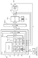
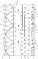
- Block diagram schematically showing an example of a system configuration including a rotating electrical machine control device Block diagram schematically showing a configuration example of a rotary electric machine drive apparatus including an inverter Explanatory drawing showing the principle of continuous pulse width modulation
- a drive source of a vehicle such as a hybrid vehicle or an electric vehicle and a rotating electrical machine control device for controlling a rotating electrical machine serving as a regenerative source to DC power supply of the vehicle.
- a rotating electrical machine control device controls a rotating electrical machine mounted on a hybrid vehicle in which an internal combustion engine and a rotating electrical machine cooperate with each other
- the present invention can be applied to a rotating electric machine control device that controls a plurality of rotating electric machines. is there.
- the rotary electric machine will be referred to as a motor as appropriate, but this refers to a rotary electric machine functioning as a motor and a generator.
- FIG. 1 schematically shows an example of a system configuration of a vehicle including such a control device 50 of a motor M (a rotating electrical machine control device).
- a three-phase synchronous motor M is provided as an AC rotating electric machine.
- the motor M is electrically connected to a DC power supply 3 via a rotary electric drive 1 provided with an inverter 5.
- the direct current power supply 3 may be a battery or may include a battery and a converter for boosting the output voltage of the battery.
- a battery is illustrated as the DC power supply 3.
- the inverter 5 converts DC power output from the DC power supply 3 into three-phase AC power (polyphase AC power).
- a motor M functioning as a motor is driven by the converted three-phase AC power. Further, when the motor M functions as a generator, the inverter 5 converts the generated three-phase AC power into DC power and regenerates the DC power supply 3.
- the inverter 5 is constituted by a bridge circuit of a plurality of phases (here, three phases) using switching elements as well known. It is preferable to apply an IGBT (insulated gate bipolar transistor) or a MOSFET (metal oxide semiconductor field effect transistor) to the switching element. In the present embodiment, the case of using an IGBT as a switching element will be described as an example.
- a leg for one phase in which two IGBTs are connected in series is configured between the DC positive electrode side and the DC negative electrode side of the inverter 5, and this leg is connected in three lines in parallel Be done. That is, a bridge circuit in which one set of legs corresponds to each of the stator coils corresponding to the U, V, and W phases of the motor M is configured.
- the collectors of the IGBTs (E1, E3, E5) on the upper side of each leg are connected to the DC positive side of the inverter 5, and the emitters are connected to the collectors of the IGBTs (E2, E4, E6) on the lower side of each leg .
- the emitters of the IGBTs (E2, E4, E6) on the lower side of each leg are connected to the DC negative side (for example, the ground) of the inverter 5.
- the middle point of the paired IGBTs in each leg that is, the connection point of the IGBTs is connected to the three-phase stator coil of the motor M, respectively.
- Freewheeling diodes (refluxing diodes) are connected in parallel (antiparallel) to the IGBTs in such a manner that the cathode terminal is connected to the collector terminal of the IGBT and the anode terminal is connected to the emitter terminal of the IGBT.
- the gate of each IGBT is connected to an electronic control unit (ECU) 50 via a driver circuit 55 described later, and is individually switching-controlled.
- ECU electronice control unit
- the ECU 50 is configured around a logic circuit such as a microcomputer.
- the ECU 50 is configured to include a CPU (central processing unit) 51 which is a microcomputer, an interface circuit 52, and other peripheral circuits and the like.
- the CPU 51 is a computer that executes a rotating electrical machine control program, and is a core of the control device 50 corresponding to the rotating electrical machine control device of the present invention.
- the interface circuit 52 is configured by an EMI (electro-magnetic interference) countermeasure component, a buffer circuit, and the like.
- the driver circuit 55 is a circuit that converts voltages of drive signals (switching control signals S1 to S6) for driving the switching elements E1 to E6 of the inverter 5.
- a drive signal input to a control terminal (gate) of an IGBT or MOSFET that switches high voltage requires a voltage higher than the power supply voltage of a general electronic circuit such as a microcomputer. Therefore, the drive signal is voltage-converted (for example, boosted) via the driver circuit 55 and then input to the inverter 5.
- the CPU 51 of this embodiment includes, for example, a CPU core 11, a program memory 12, a parameter memory 13, a work memory 14, a communication control unit 15, an A / D converter 16, a timer 17, and a port 18. It is configured to have.
- the CPU core 11 is a core of the CPU 51, and includes an instruction register, an instruction decoder, an ALU (arithmetic logic unit) as an execution subject of various operations, a flag register, a general purpose register, an interrupt controller, and the like. That is, the core of the control device 50 is realized by the cooperation of hardware mainly including the CPU core 11 and the work memory 14 and the timer 17 and software such as a program and parameters stored in the program memory 12 and the parameter memory 13. Configured
- the program memory 12 is a non-volatile memory in which a motor control program (a rotating electrical machine control program) is stored.
- the parameter memory 13 is a non-volatile memory in which various parameters referred to when executing a program are stored.
- the parameter memory 13 may be constructed without being distinguished from the program memory 12.
- the program memory 12 and the parameter memory 13 are preferably configured by, for example, a flash memory or the like.
- the work memory 14 is a memory for temporarily storing temporary data during program execution.
- the work memory 14 is composed of a dynamic RAM (DRAM) and a static RAM (SRAM) that can read and write data at high speed without problems due to volatility.
- DRAM dynamic RAM
- SRAM static RAM
- the communication control unit 15 controls communication with other systems in the vehicle. For example, communication with the traveling control system 60 and other systems, sensors, and the like is controlled via a network such as a CAN (controller area network) in the vehicle.
- the CPU 51 receives the motor control instruction Hr (for example, a required torque for the motor M) from the traveling control system 60 via the communication control unit 15, and controls the motor M based on this.
- the A / D converter 16 converts an analog electrical signal into digital data.
- the detection result of the motor current flowing in each stator coil of the motor M is received from the current sensor 58 and converted into digital data.
- the case where all the three-phase currents of the U, V, and W phases are detected by the non-contact current sensor 58 is illustrated. However, since the three-phase current is balanced and its instantaneous value is zero, currents of only two phases may be detected, and the remaining one phase may be calculated by the CPU 51.
- the A / D converter 16 is illustrated as having a plurality of analog inputs, but it is not necessary to have a plurality of inputs.
- the interface circuit 52 may be provided with a multiplexer to obtain a plurality of current values by time division.
- vector control As a method of controlling an AC motor, a control method called vector control is known.
- vector control the first axis according to the direction of the magnetic field generated by the permanent magnet disposed in the rotor (for example, d along the direction of the magnetic field) is applied to the coil current flowing through the three-phase stator coils of the AC motor.
- the feedback control is performed by coordinate conversion into a two-phase vector component of an axis) and a second axis (for example, the q axis) orthogonal to the first axis.
- dq axis vector space dq axis orthogonal coordinate system
- a rotation detection sensor 59 such as a resolver is provided in the vicinity of the motor M.
- the detection result is transmitted to the register in the CPU core 11 and the work memory 14 through the port 18 of the CPU 51 as described above.
- the control device 50 obtains a rotor position (electrical angle ⁇ ) and a rotational speed (angular velocity ⁇ ) based on the rotation detection signal R of the rotation detection sensor 59.
- the rotation detection sensor 59 may directly output the electrical angle ⁇ or the angular velocity ⁇ .
- the control device 50 is configured to include an inverter control unit 10 as a functional unit that controls the rotary electric machine drive device including the inverter 5 by vector control.
- Inverter control unit 10 calculates a torque command, which is a required torque for controlling each motor M, based on a motor control command (travel control command) Hr given from travel control system 60, and responds to each torque command.
- a torque command which is a required torque for controlling each motor M
- Hr motor control command
- current commands id and iq which are two-phase target currents for current feedback control, are set.
- the current commands id and iq are target currents set corresponding to the d axis and the q axis described above.
- the inverter control unit 10 performs, for example, proportional integral control (PI control) or proportional integral derivative control (PID control) based on the deviation between the current command id, iq and the feedback motor current, and The voltage commands vd and vq which are voltages are set. Since the motor current detected by the current sensor 58 is a three-phase current, it is coordinate-converted to the two-phase currents Id and Iq based on the electrical angle ⁇ . Then, PID control is performed based on the deviation between the current command id, iq and the two-phase motor current Id, Iq, and the angular velocity ⁇ , and the voltage command vd, vq is calculated.
- PI control proportional integral control
- PID control proportional integral derivative control
- inverter control unit 10 Based on voltage commands vd and vq, inverter control unit 10 generates switching control signals S1 to S6 (modulated pulses) for driving the three-phase IGBTs of inverter 5.
- the inverter control unit 10 coordinate-converts the two-phase voltage commands vd, vq into three-phase voltage commands Vu, Vv, Vw based on the electrical angle ⁇ .
- inverter control unit 10 generates switching control signals S1 to S6 of the IGBTs constituting inverter 5.
- the switching control signals S1 to S6 are generated by pulse width modulation.
- Pulse width modulation includes methods such as continuous pulse width modulation (CPWM: continuous PWM) such as sine wave pulse width modulation or space vector pulse width modulation; discontinuous pulse width modulation (DPWM: discontinuous PWM).
- CPWM continuous pulse width modulation
- DPWM discontinuous pulse width modulation
- CPWM is a method of changing the signal levels of switching control signals corresponding to other two phases by sequentially fixing the signal levels of the switching control signals of the inverter corresponding to one phase of the AC power of three phases.
- CPWM is a scheme in which all phases are modulated without fixing the switching control signal corresponding to one of the phases.
- the operating conditions such as the rotational speed and torque required for the motor M, and the modulation factor required to satisfy the operating conditions (ratio of DC voltage to effective value of interphase voltage of three-phase AC) It is decided according to Here, the case where CPWM is selected as the modulation method will be described.
- the upper part shows the relationship between carrier CA and voltage commands Vu, Vv and Vw of three phases
- the lower part shows switching control signals S1, S3 and S5 (modulated pulses) of three phases.
- the switching control signal S1 for driving the switching element E1 of the upper arm in the U phase has a signal level at high level (H) when the voltage command Vu in U phase is higher than the carrier CA, and the voltage command Vu is smaller than the carrier CA Is a modulation pulse whose signal level is low (L).
- Switching control signal S3 for driving switching element E3 of the upper arm of V phase and switching control signal S5 for driving switching element E5 of the upper arm of W phase are similarly carrier CA, voltage command Vv, and voltage command It is generated based on Vw.
- switching control signals S1, S3, and S5 are treated as a representative as three-phase switching control signals (modulation pulses).
- Inverter control unit 10 generates modulation pulses by pulse width modulation (CPWM) according to a predetermined modulation frequency as drive signals of switching elements E1 to E6 of the plurality of phases of inverter 5 corresponding to AC powers of a plurality of phases. , Control the inverter 5.
- CPWM pulse width modulation
- a section including a single-phase active vector section and a phase in which the signal level is high and a phase in which the signal level is low is referred to as an “active vector section”.
- Single-phase active vectors, zero vectors and active vectors defining these intervals are space vectors in vector control.
- space vectors can be defined by a combination of signal levels of switching control signals S1, S3 and S5 of the upper arm.
- the space vector indicated by (UVW) is the following eight. That is, there are eight of (000), (001), (010), (011), (100), (101), (110), and (111).
- the three-phase switching control signals S2, S4 and S6 of the lower arm have signal levels complementary to the switching control signals S1, S3 and S5 of the upper arm, respectively. Accordingly, space vectors for switching control of the three-phase inverter 5 are represented by the eight described above.
- space vectors (000) and (111) are called zero vectors or null vectors because the interphase voltage is zero and no current flows in the motor M.
- the other six space vectors are called active vectors.
- active vectors a space vector in which only one of U, V and W phases is "1", (001), (010) and (100) are one of multiple phases. It is a space vector when the signal level of only the modulation pulse is high level. Therefore, these three space vectors are referred to as "single-phase active vectors".
- the single-phase active vector appears in a region where the values of the voltage commands Vu, Vv, and Vw are high, as shown by a dashed region G in FIG.
- FIG. 3 schematically shows the U-phase current Iu.
- the current increases during a period other than the zero vector (active vector period including the single-phase active vector period MAV), and no current flows through the stator coil in the zero vector period NV. That is, in the active vector section, the DC power supply 3 and the motor M are connected via the inverter 5 and current flows, but in the zero vector section NV, no current flows between the DC power supply 3 and the motor M. This is because the current flows back between the motor 5 and the motor M. The current flowing back between the inverter 5 and the motor M is consumed due to resistance loss and the like. As is apparent from the waveform of U-phase current Iu in FIG.
- a ripple occurs in the current flowing through the stator coil of motor M since a difference occurs between the current in the active vector section and the zero vector section NV.
- the amplitude of this ripple corresponds to the increase and decrease of the current between the active vector section and the zero vector section NV.
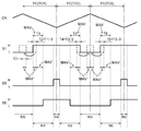
- FIG. 4 schematically shows waveforms of the switching control signals S1, S3 and S5 in which the period including the single-phase active vector section MAV is expanded.
- the inverter control unit 10 generates a modulation pulse according to a predetermined modulation frequency by the CPWM method.
- This modulation frequency is the frequency of the carrier CA shown in FIG. 3 and FIG.
- the modulation pulse is defined as a half period of the carrier CA, that is, a period in which the waveform of the carrier CA of the triangular wave travels from a valley (bottom) to a peak (peak) and a period from the peak to the valley.
- the inverter control unit 10 reduces the amplitude of the ripple current by suppressing the increase and decrease of the current between the active vector section and the zero vector section NV. Specifically, by increasing the frequency of the ripple current, the amplitude per period of the ripple current is suppressed.
- One way to increase the frequency of the ripple current is to increase the frequency of the carrier CA. However, if the frequency of the carrier CA is simply increased, the number of times of switching of the switching elements E1 to E6 in the inverter 5 increases to increase the switching loss. Therefore, in the present embodiment, the frequency of the ripple current is increased by raising the frequency of the carrier CA of only one phase among the plurality of phases. In the present embodiment, the frequency of the carrier CA of only one phase is virtually increased by setting the single-phase active vector section MAV during the zero vector section NV represented by the space vector (000).
- the single phase active vector period MAV when the single phase active vector period MAV is included in the above-mentioned standard modulation period TC, the single phase active vector period MAV is divided and distributed to different timings in the same standard modulation period TC. As shown in FIG. 4, when the single phase active vector period MAV is included in the reference modulation period TC, the zero vector period NV where the signal level of all phases is low level in the reference modulation period TC. Exists. Therefore, the single-phase active vector section MAV after division is arranged in the zero vector section NV.
- the inverter control unit 10 changes the signal level once between the high level and the low level in each of the reference modulation periods TC.
- the switching control signals S1, S3 and S5 are all at low level to high level in the reference modulation period TC corresponding to the downward period (first period TC1) in which the carrier CA goes from mountain to valley.
- the reference modulation period TC corresponding to the rising period (second period TC2) going from valley to mountain
- the carrier CA changes once from high level to low level.
- the designation of the first period and the second period with respect to the downlink period and the uplink period of the carrier CA is merely for distinction and does not define any order. As a matter of course, the names of the first period and the second period may be reversed.
- the first period TC1 starts from the zero vector section NV where the signal levels of all phases are low level, and the switching control signal S1 first becomes high level, and then the switching control signal S5 and switching control signal S3 become high level in this order. Become. That is, the head of the first period TC1 is the zero-vector section NV of the all phase low level, passes through the single-phase active vector section MAV and the active vector section, and the tail becomes the zero-vector section NV of the all phase high level.
- the second period TC2 starts from the zero vector section NV where the signal levels of all phases are high, and becomes low in order of the switching control signal S3, the switching control signal S5, and the switching control signal S1.
- the head of the second period TC2 is the zero-vector section NV of all phases high level, the active vector section and the single-phase active vector section MAV, and the tail is the zero-vector section NV of all phases low level.
- the reference modulation period TC shown in FIG. 4 there is a single-phase active vector section MAV in which only the switching control signal S1 is at high level and the switching control signals S3 and S5 are at low level.
- the inverter control unit 10 divides the single-phase active vector section MAV into a plurality (here, two) in the reference modulation period TC including the single-phase active vector section MAV, and sets the zero vector of the same reference modulation period TC. Allocate within the range of interval NV. Specifically, the divided single-phase active vector section MAV is distributed to the side where the signal level is low among the beginning and the end of the reference modulation period TC. That is, as in the first period TC1 of FIG. 4, when the signal level of the modulation pulse to be divided and distributed is low level at the beginning of the reference modulation period TC, the inverter control unit 10 performs the reference modulation period TC.
- one divided single-phase active vector section MAV is allocated to the end of the reference modulation period TC.
- inverter control unit 10 includes a section (MAV ′) to be left on the side where single-phase active vector section MAV before division exists in reference modulation period TC and a section (MAV ′ ′) to be distributed to other positions.
- the single-phase active vector section MAV is divided so that the ratio thereof to 2 to 1 becomes 2. As shown in FIG.4, it is 1/3 of the period T1 of the single-phase active vector section MAV of the first period TC1.
- a section (MAV ′ ′) having a corresponding period T2 is allocated to the head of the first period TC1, and a section (MAV ′) corresponding to 2 ⁇ 3 remains at the original position.
- a section (MAV ′ ′) having a period T4 corresponding to 1 ⁇ 3 is distributed at the end of the second period TC2
- the corresponding interval (MAV ') remains at the original position.
- a period T5 of the single-phase active vector period MAV of the first period (hereinafter, referred to as "third period TC3" for the sake of distinction) subsequent to the second period TC2 which is the uplink period is It is assumed that it is the same as the period T3 of the single phase active vector section MAV of the second period TC2.
- the period T6 corresponding to 1/3 of the period T5 of the single-phase active vector period MAV of the third period TC3 is distributed to the head of the third period TC3 (MAV ′ ′), and 2/3 remains at the original position (MAV)
- the total length of the single-phase active vector section MAV included in the second period TC2 and the third period TC3 is the same before and after the division (see FIG.
- the sum of single-phase active vector sections MAV and the sum of lengths of active vector sections are the same before and after division / distribution of single-phase active vector section MAV. Therefore, the three-phase line voltage is maintained before and after division and distribution of the single-phase active vector section MAV, and a voltage equivalent to that before division and distribution can be applied to the motor M. That is, it is possible to suppress the ripple current while maintaining the voltage applied to the motor M.
- the inverter control unit 10 of the present embodiment is configured with the CPU 51 as the core.
- the carrier CA is virtually realized by the timer 17 (synonymous with the counter), a register cooperating with the timer 17, or the like. Specifically, as shown in the lower part of FIG.
- the reference modulation period TC is set by 100 counts of 0 to 99 in decimal is illustrated.
- the distinction between the downlink period (first period TC1) and the uplink period (second period TC2) is defined by another count value CTS.
- the case where the count value CTS is "0" is the down period (first period TC1)
- the case where the count value CTS is "1" is the up period (second period TC2).
- the distinction between the downlink period and the uplink period may be represented by the upper bits of the same count value, and the length of the reference modulation period TC may be represented by the lower bits.
- an example is given in which both the uplink period and the downlink period are defined by the up counter method in which the value increases.
- the uplink period is defined by the up counter method
- the downlink period is decreased by the value It may be defined by a counter method. When such an up / down counter method is adopted, it is possible to express peaks and valleys by the count value.
- the first period TC1 “29” is set as the voltage command Vu of the switching control signal S1
- “89” is set as the voltage command Vv of the switching control signal S3, and as the voltage command Vw of the switching control signal S5. It is assumed that "59” is set.
- the signal levels at the beginning of the first period TC1 are all low level, and the length of the low level from the beginning of the first period TC1 of each modulation pulse is "30" for the switching control signal S1, and the switching control signal S3. Is “90”, and the switching control signal S5 is “60”.
- the period T1 of the single-phase active vector section MAV has a length corresponding to "30" of the count value CT.
- T1 30.
- voltage command Vu includes information “L” (or “0”) indicating the signal level at the beginning of reference modulation period TC, and information “29” indicating one change point in the period. It is configured to have.
- the voltage command Vu further has information indicating another change point Adjusted to
- the signal level at the beginning of the reference modulation period TC is changed to change from high level to low level through the period T2.
- voltage command Vu includes information “H” (or “1”) indicating the signal level at the beginning of reference modulation period TC, and information “69” indicating one change point in the period. It is configured.
- voltage command Vu is further adjusted to have information indicating one more change point.
- the inverter control unit 10 when division and allocation are completed in each reference modulation period TC as described above, the influence on the program is also small, which is preferable. It is. That is, it is possible to suppress the ripple current using substantially the same program as in the case where division / distribution of the single-phase active vector section MAV is not performed. In each reference modulation period TC, the ratio of the single-phase active vector section MAV is maintained. Therefore, it is possible to suppress the ripple current in a state in which the three-phase interphase voltage applied to the motor M is maintained before and after division / distribution of the single phase active vector section MAV.
- the single-phase active vector section MAV is not actually increased without increasing the frequency of the carrier CA or shortening the cycle of the reference modulation period TC.
- the modulation frequency of the modulation pulse of only one phase is made higher (sub modulation frequency) than the modulation frequency of the other phase. That is, by shaping the waveform, modulation pulses of only one phase are generated as pulses having a submodulation frequency higher than that of modulation pulses of other phases.
- a modulation pulse of only one phase may be generated using subcarrier CA 'according to the submodulation frequency higher than the modulation frequency of carrier CA.
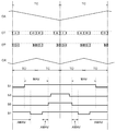
- FIG. 7 exemplarily shows a method of using a microcomputer or the like to generate a modulation pulse according to the submodulation frequency higher than the modulation frequency of the carrier CA.
- FIG. 7 shows the carrier CA and the count value CT of the timer 17 that virtually realizes the carrier CA, as in FIG.
- this count value CT is converted into a subcount value CT '.
- the sub count value CT ' is set such that the period corresponding to "1" of the count value CT is the period corresponding to "2" of the sub count value CT'. That is, the sub-count value CT 'is the output value of the counter (timer) which advances twice faster than the count value CT.
- the subcount value CT ′ virtually realizes the subcarrier CA ′ in the same way as the count value CT virtually realizes the carrier CA. That is, as shown in FIG.
- the subcarrier CA 'of the sub modulation frequency higher (here, twice) than the modulation frequency of the carrier CA is obtained.
- the upstream period or the downstream period of the subcarrier CA ' is a sub reference modulation period TC' which is 1/2 the length of the reference modulation period TC.
- the reference modulation period TC includes two sub reference modulation periods TC '.
- voltage commands Vu, Vv, Vw are set in each reference modulation period TC, and switching control signals S1, S3, S5 are generated according to these voltage commands Vu, Vv, Vw.
- the switching control signal of only one phase (U phase) constituting the single phase active vector section MAV is generated as the adjusted switching control signal S1 'based on the subcarrier CA' of the sub modulation frequency. Then, the adjusted switching control signal S1 'switches the switching element E1 as the switching control signal S1.
- FIG. 7 shows a single-phase active vector section MAV determined by the relationship between the switching control signal S1 generated based on the reference modulation period TC and the other two phase switching control signals S3 and S5, and the sub reference modulation period TC ′. And both of the adjusted single-phase active vector section AMAV, which is determined by the relationship between the adjusted switching control signal S1 'generated on the basis of the other two-phase switching control signals S3 and S5.
- the modulation pulse of the U phase is the sum of the total length of the single phase active vector section MAV in two cycles of the reference modulation period TC, that is, one cycle of the carrier CA and the length of the adjusted single phase active vector section AMAV.
- the case of the switching control signal S1 is the same as the case of the adjusted switching control signal S1 '.
- the inverter control unit 10 generates a modulation pulse based on the sub modulation frequency, including division and distribution, as a result of which the dead time period can not be satisfied.
- the generation of the modulation pulse based on the sub modulation frequency may not be performed including the division and distribution of the section MAV.
- the section allocated to another position after division. (MAV ′ ′) is continuous at the end of the preceding reference modulation period TC and at the beginning of the subsequent reference modulation period TC, and becomes one single-phase active vector section MAV.
- a single reference modulation period Even if the section (MAV ′ ′) divided at TC and allocated to the head or the end (MAV ′ ′) is not longer than the dead time period, the single-phase active vector section MAV synthesized into one across adjacent reference modulation periods TC is dead It may be more than the time period.
- each reference modulation period TC single-phase active that is synthesized into one over adjacent reference modulation period TC instead of determining that the section after division (MAV ′ ′) is equal to or longer than the dead time period. It may be determined that the vector interval MAV is greater than or equal to the dead time period.
- a three-phase alternating current rotating electrical machine is described as an example of the motor M, but the present invention can be applied to a polyphase alternating current rotating electrical machine having more than three phases by those skilled in the art.
- the present invention can also be applied to a rotating electrical machine control device that controls a multiphase AC rotating electrical machine having more than three phases.
- the modulation frequency for generating the modulation pulse of only one phase may be higher than the modulation frequency of the other phase, for example, maintaining the modulation frequency for generating the modulation pulse of only one phase, the modulation frequency may be maintained.
- the modulation frequency of the other phase may be reduced. As described above, since the value of the voltage command of one phase having the single-phase active vector section is high, the value of the voltage command of the other phase becomes relatively low (see FIG. 3). Therefore, reducing the modulation frequency for generating the modulation pulse of the other phase has little effect.
- the modulation frequency of one phase is 1 and the modulation frequency of the other two phases is 1/2
- the modulation frequency is 2/3 as a whole and the ripple current is suppressed.
- Switching loss can also be reduced.
- Such a change in modulation frequency is also preferred if the resolution of the modulation can be reduced.
- the modulation frequency of only one phase is doubled in the three-phase alternating current and the modulation frequency of the other phase is maintained at 1 ⁇
- the modulation frequency is 4/3 as a whole.
- the switching loss is 4/3 while suppressing the ripple current.
- the modulation frequency of all three phases is doubled, the switching loss as a whole will be doubled. Therefore, by increasing the modulation frequency of only one phase and maintaining the modulation frequency of the other phase, it is possible to suppress an increase in switching loss while well suppressing the ripple current.
- the present invention is a rotating electrical machine drive apparatus including an inverter interposed between a DC power supply and an AC rotating electrical machine to convert power between DC power of the DC power supply and AC power of multiple phases of the rotating electrical machine. It is applicable to the rotary electric machine control device to control.
- Rotary electric machine drive device 3 DC power supply 5: Inverter 10: Inverter control unit 56: DC power supply 50: Control device (Rotary electric machine control device) MAV: single-phase active vector section MAV ′: single-phase active vector section MAV ′ ′: single-phase active vector section AMAV: single-phase active vector section E1 to E6 after adjustment: switching element Iu: U-phase current M: motors S1 to S6: Switching control signal (modulated pulse)
- CA Carrier CA ': Subcarrier TC: Reference modulation period TC': Sub-reference modulation period
Landscapes
- Engineering & Computer Science (AREA)
- Power Engineering (AREA)
- Control Of Ac Motors In General (AREA)
- Inverter Devices (AREA)
Abstract
インバータを連続パルス幅変調方式で駆動する際の電流リップルを低減する。複数相の交流電力に対応するインバータの駆動信号として、所定の変調周波数に応じたパルス幅変調により変調パルスを生成するインバータ制御部は、変調周波数に基づく基準変調期間TCに、複数相の内の1相のみの変調パルスの信号レベルがハイレベルとなる単相アクティブベクトル区間MAVを含む場合、単相アクティブベクトル区間MAVを含む基準変調期間TCにおいて単相アクティブベクトル区間MAVに信号レベルがハイレベルとなる1相のみの変調パルスS1を、他の相の変調周波数よりも高い副変調周波数に応じて生成する。
Description
本発明は、直流電源の直流電力と回転電機の複数相の交流電力との間で電力変換するインバータを備えた回転電機駆動装置を制御する回転電機制御装置に関する。
インバータを備えた回転電機駆動装置を制御する制御装置では、多くの場合パルス幅変調(PWM:pulse width modulation)制御が実施される。パルス幅変調では、出力させる交流電力の波形に応じた電圧指令と、例えば三角波などのキャリア(搬送波)との比較により、矩形パルスを生成して電圧指令を離散的なパルス信号に変調する。インバータを構成するスイッチング素子は、このようなパルス信号によってスイッチングされるため、出力される交流電力の波形は、滑らかな正弦波状とはならず、微細な変動を含んでいる。このような変動成分をリップルと称し、回転電機を流れる電流に生じるリップルをリップル電流と称する。このリップル電流は、回転電機の鉄損などの損失の原因となる。
リップル電流を抑制する方法として、パルス幅変調のキャリアの周波数を高くする方法が知られている。しかし、キャリアの周波数が高くなると、矩形パルスのパルス数が増加するため、インバータを構成するスイッチング素子のスイッチング回数も増加し、スイッチング損失が増加する。このため、例えば特開2009-291019号公報(特許文献1)には、電圧指令値が大きい領域でキャリア周波数を高く設定し、電圧指令値が小さい領域でキャリア周波数を低く設定することが提案されている(第9~12段落、請求項1、要約等)。また、特開2009-11028号公報(特許文献2)には、リップル電流(Irp)と所定の基準値(Irp#)とを比較して、リップル電流が大きいとき(Irp>Irp#)にはキャリアの周波数を上昇させ、逆にリップル電流が小さいとき(Irp≦Irp#)にはキャリアの周波数を低下させることが提案されている(図7等)。
特許文献1や特許文献2において提案された技術は、キャリア周波数を高くすることでリップル電流を低減させつつ、キャリア周波数が高くなることによるスイッチング損失の増大を、ある程度抑制可能である。但し、インバータが3相交流などの多相交流と直流との間で電力変換を行う場合、リップル電流も相ごとに発生する。また、リップル電流が最も大きい相は順次移り変わる。このため、キャリア周波数を変化させるとリップル電流が少ない相においてもスイッチング回数が増加して、リップル電流の低減に寄与することなくスイッチング損失が増加する場合がある。従って、スイッチング損失の増加を抑制しながら、より効果的にリップル電流を低減するためには改善の余地がある。
上記背景に鑑みて、インバータのスイッチング損失の増加を抑制すると共に、リップル電流を低減することが可能な技術の提供が望まれる。
上記課題に鑑みた本発明に係る回転電機制御装置の特徴構成は、
直流電源と交流の回転電機との間に介在されて前記直流電源の直流電力と前記回転電機の複数相の交流電力との間で電力変換するインバータを備えた回転電機駆動装置を制御する回転電機制御装置であって、
前記複数相の前記交流電力に対応する前記インバータの複数相のスイッチング素子の駆動信号として、所定の変調周波数に応じたパルス幅変調により変調パルスを生成して、前記インバータを制御するインバータ制御部を備え、
前記インバータ制御部は、前記変調周波数に基づく基準変調期間に、前記複数相の内の1相のみの前記変調パルスの信号レベルがハイレベルとなる単相アクティブベクトル区間を含む場合、当該単相アクティブベクトル区間を含む前記基準変調期間において当該単相アクティブベクトル区間に信号レベルがハイレベルとなる1相のみの前記変調パルスを、他の相の前記変調周波数よりも高い副変調周波数に応じて生成する点にある。即ち、前記インバータ制御部は、前記変調周波数に基づく基準変調期間に、前記複数相の内の1相のみの前記変調パルスの信号レベルがハイレベルとなる単相アクティブベクトル区間を含む場合、当該単相アクティブベクトル区間を含む前記基準変調期間において当該単相アクティブベクトル区間に信号レベルがハイレベルとなる1相のみの前記変調パルスを、他の相の前記変調周波数よりも高い副変調周波数を有するパルスとして生成する。
直流電源と交流の回転電機との間に介在されて前記直流電源の直流電力と前記回転電機の複数相の交流電力との間で電力変換するインバータを備えた回転電機駆動装置を制御する回転電機制御装置であって、
前記複数相の前記交流電力に対応する前記インバータの複数相のスイッチング素子の駆動信号として、所定の変調周波数に応じたパルス幅変調により変調パルスを生成して、前記インバータを制御するインバータ制御部を備え、
前記インバータ制御部は、前記変調周波数に基づく基準変調期間に、前記複数相の内の1相のみの前記変調パルスの信号レベルがハイレベルとなる単相アクティブベクトル区間を含む場合、当該単相アクティブベクトル区間を含む前記基準変調期間において当該単相アクティブベクトル区間に信号レベルがハイレベルとなる1相のみの前記変調パルスを、他の相の前記変調周波数よりも高い副変調周波数に応じて生成する点にある。即ち、前記インバータ制御部は、前記変調周波数に基づく基準変調期間に、前記複数相の内の1相のみの前記変調パルスの信号レベルがハイレベルとなる単相アクティブベクトル区間を含む場合、当該単相アクティブベクトル区間を含む前記基準変調期間において当該単相アクティブベクトル区間に信号レベルがハイレベルとなる1相のみの前記変調パルスを、他の相の前記変調周波数よりも高い副変調周波数を有するパルスとして生成する。
この特徴構成によれば、変調周波数に基づく基準変調期間、例えば、キャリアの1周期や半周期、2周期などに相当する期間に、単相アクティブベクトル区間を含む場合にのみ、変調周波数よりも高い副変調周波数による変調が行われる。即ち、変調周波数よりも高い副変調周波数を有するパルスとして、変調パルスが生成される。その結果、相対的に変調周波数が低い場合には変調周波数が高い場合に比べて単相アクティブベクトル区間の継続時間が長くなる。単相アクティブベクトル区間には電流が増加するが、この継続時間が相対的に長い場合は、短い場合に比べて電流の増加量も大きくなる。このため、単相アクティブベクトル区間と、単相アクティブベクトル区間ではない区間との電流の差が大きくなり、リップル電流の振幅が大きくなる。本特徴構成のように、変調周波数よりも高い副変調周波数によって変調するようにすることで、単相アクティブベクトル区間の継続時間を短くすることができるので、この単相アクティブベクトル区間における電流の増加量が抑制される。その結果、単相アクティブベクトル区間と、単相アクティブベクトル区間ではない区間との電流の差が小さくなり、リップル電流の振幅も小さくなる。
尚、変調周波数を高くしているだけであるから、1つの単相アクティブベクトル区間の継続時間は短くなるが、単相アクティブベクトル区間が出現する回数が増加するので、単相アクティブベクトル区間の総継続時間は維持される。従って、複数相の交流電力の相間電圧も変調周波数の変更に拘わらず維持される。さらに、本特徴構成によれば、当該単相アクティブベクトル区間を含む基準変調期間において当該単相アクティブベクトル区間に信号レベルがハイレベルとなる1相のみの変調パルスを生成するための変調周波数が副変調周波数に変更され、他の相の変調周波数は変わらない。つまり、インバータのスイッチング損失の増加は、当該1相のみに限定されるから、スイッチング損失の増加が抑制される。このように、本特徴構成によれば、インバータのスイッチング損失の増加を抑制すると共に、リップル電流を低減することが可能となる。
多くの場合、基準変調期間の中で1カ所にしか出現しない単相アクティブベクトル区間を2カ所以上に分割して配分すれば、基準変調期間を2つ以上に分割したこととほぼ等価となる。基準変調期間は、変調周波数に基づく期間であるから、基準変調期間を2つ以上に分割することは、変調周波数を高くすることとほぼ等価である。従って、1つの態様として、本発明に係る回転電機制御装置の前記インバータ制御部は、前記単相アクティブベクトル区間を、当該単相アクティブベクトル区間を含む前記基準変調期間の中で複数に分割して配分すると好適である。
ここで、1つの態様として、本発明に係る回転電機制御装置の前記インバータ制御部が、前記基準変調期間のそれぞれにおいて前記信号レベルを1回変化させるものである場合、前記インバータ制御部は、前記基準変調期間の先頭及び末尾の内、信号レベルがローレベルである側に、分割した前記単相アクティブベクトル区間を配分すると好適である。この態様によれば、基準変調期間のそれぞれにおいて変調パルスの信号レベルが1回変化するので、基準変調期間の先頭でハイレベルであれば末尾ではローレベルとなり、先頭でローレベルであれば末尾ではハイレベルとなる。従って、ある基準変調期間の先頭側に単相アクティブベクトル区間が存在するとき(先頭においてハイレベルであるとき)、当該基準変調期間の末尾には単相アクティブベクトルは存在せず、信号レベルはローレベルとなる。一方、この基準変調期間に続く基準変調期間では、変調パルスはローレベルから始まり、信号レベルが変化してハイレベルで終わる。つまり、変調パルスは、この基準変調期間の先頭でローレベルであり、末尾でハイレベルである。
上述したように、1つの態様として、1つの基準変調期間において、分割前に単相アクティブベクトル区間が存在する側とは異なる側である、信号レベルがローレベルである側に、分割した前記単相アクティブベクトル区間を配分することができる。例えば、基準変調期間の先頭に単相アクティブベクトル区間が存在する場合には、末尾の信号レベルがローレベルであり、当該基準変調期間の末尾に分割後の単相アクティブベクトル区間が配分される。また、基準変調周期の末尾に単相アクティブベクトル区間が存在する場合には、先頭の信号レベルがローレベルであり、当該基準変調期間の先頭に分割後の単相アクティブベクトル区間が配分される。この態様によれば、当該基準変調期間の先頭と末尾とに単相アクティブベクトル区間が存在することとなり、仮想的に基準変調期間が2つに分割されることとなって変調周波数を高くすることになる。つまり、この態様によれば、基準変調期間やキャリアを変更することなく、簡単な基準に基づいて単相アクティブ区間を分割し、配分することによって、インバータのスイッチング損失の増加を抑制すると共に、リップル電流を低減することが可能となる。
ところで、基準変調期間のそれぞれにおいて、信号レベルが1回だけ変化する場合、変調パルスの信号レベルが、基準変調期間の先頭でハイレベルであれば末尾ではローレベルとなり、先頭でローレベルであれば末尾ではハイレベルとなる。従って、アクティブベクトル区間が、ある基準変調期間(Xとする)の先頭側に存在すると、次の基準変調期間(Yとする)の先頭側には単相アクティブベクトル区間は存在しない。当該次の基準変調期間(Y)にアクティブベクトル区間が存在する場合には、末尾側に存在することになる。ここで、基準変調期間の先頭側に存在するアクティブベクトル区間(Aとする)を分割すると、分割後の単相アクティブベクトル区間の一方(A’とする)は元の位置に残され、他方(A”とする)は末尾に配分される。一方、この基準変調期間(X)の次の基準変調期間(Y)の末尾側に存在するアクティブベクトル区間(Bとする)を分割すると、分割後の単相アクティブベクトル区間の一方(B’とする)は元の位置に残され、他方(B”とする)は先頭に配分される。つまり、隣接する2つの基準変調期間(X,Y)において分割後に元の位置とは異なる位置へ配分される各単相アクティブベクトル区間(A”,B”)は、2つの基準変調期間(X,Y)の境において連続し、1つのアクティブベクトル区間(C=A”+B”)となる。
ここで、分割前の2つの単相アクティブベクトル区間(A,B)の長さが同じであると仮定する。そして、A’とA”、B’とB”との比率が“2:1”となるように元のアクティブベクトル区間が分割されると、A’とB’とC(=A”+B”)との長さが同一であるから、“A’:B’:C=1:1:1”となる。つまり、2つのアクティブベクトル区間が均等に3つのアクティブベクトル区間に配分される。尚、分割前の2つの単相アクティブベクトル区間(A,B)の長さが異なっていても、各アクティブベクトル区間から一定の割合で異なる位置へ配分されることになるから、全体としてアクティブベクトル区間は、ほぼ均等に設定されることになる。また、2つの単相アクティブベクトル区間を3つの単相アクティブベクトル区間に再配分しているが、これは、2つのアクティブベクトル区間の中間に1つずつ新たなアクティブベクトル区間を設定していくことと、ほぼ等価である。従って、アクティブベクトル区間の間隔がほぼ均等となり、リップル電流の振幅もほぼ一定に抑制される。このように、1つの態様として、本発明に係る回転電機制御装置の前記インバータ制御部は、前記基準変調期間において分割前の前記単相アクティブベクトル区間が存在する側に残す区間と別の側に配分される区間との比が2対1となるように、前記単相アクティブベクトル区間を分割すると好適である。
また、本発明に係る回転電機制御装置は、前記副変調周波数に応じて生成された前記変調パルスに含まれる前記単相アクティブベクトル区間が、前記信号レベルをハイレベルとローレベルとの間で変化させる際に、前記インバータの1相のレッグを構成する上段側アームの前記スイッチング素子及び下段側アームの前記スイッチング素子が共にオフ状態にスイッチングされる期間であるデッドタイム期間以上の長さに設定されると好適である。直流電源の正極と負極との間に直列接続されて相補的にオン状態となる上段側アームのスイッチング素子と下段側アームのスイッチング素子とは、両アームのスイッチング素子が一時的にでも同時にオン状態となった場合に、直流電源を短絡させてしまう。従って、両アームスイッチング素子の一方がオン状態からオフ状態へ、他方がオフ状態からオン状態へと遷移する際には、両アームのスイッチング素子が共にオフ状態となるようにスイッチングされる期間であるデッドタイム期間が設定される。このデッドタイム期間は、インバータの安全性を確保するために必ず設けなければならない期間であるから、分割後の単相アクティブベクトル区間の長さは、このデッドタイム期間以上の長さに設定されると好適である。尚、1つの態様として、インバータ制御部は、分割後の単相アクティブベクトル区間の長さがこのデッドタイム期間以上の長さに設定可能か否かに応じて、単相アクティブベクトル区間の分割を行うか否かを決定するようにしてもよい。
以下、本発明の実施形態を、ハイブリッド自動車や電気自動車などの車両の駆動源及び当該車両の直流電源への回生源となる回転電機を制御する回転電機制御装置を例として、図面に基づいて説明する。本実施形態では、回転電機制御装置が、内燃機関と回転電機とが協働するハイブリッド自動車に搭載される回転電機を制御する場合を例として説明する。説明を容易にするために、本実施形態では、1つの回転電機を制御する場合を例として説明するが、複数の回転電機を制御する回転電機制御装置にも本発明を適用することが可能である。尚、以下、回転電機を適宜、モータと称して説明するが、これは、電動機及び発電機として機能する回転電機を指す。
図1のブロック図は、そのようなモータMの制御装置50(回転電機制御装置)を含む車両のシステム構成の一例を模式的に示している。図1に示すように、本実施形態では、交流の回転電機として3相同期モータMが備えられている。図1に示すように、モータMは、インバータ5を備えた回転電気駆動装置1を介して、直流電源3と電気的に接続される。この直流電源3は、バッテリであっても良いし、バッテリ及びバッテリの出力電圧を昇圧するコンバータを含むものであってもよい。本実施形態では、図2に示すように直流電源3としてバッテリを例示している。インバータ5は、直流電源3から出力される直流電力を3相交流電力(多相交流電力)に変換する。変換された3相交流電力によって、電動機として機能するモータMが駆動される。また、インバータ5は、モータMが発電機として機能する場合には、発電された3相交流電力を直流電力に変換して直流電源3に回生する。
インバータ5は、よく知られているようにスイッチング素子を用いた複数相(ここでは3相)のブリッジ回路により構成される。スイッチング素子には、IGBT(insulated gate bipolar transistor)やMOSFET(metal oxide semiconductor field effect transistor)を適用すると好適である。本実施形態では、スイッチング素子としてIGBTを用いる場合を例として説明する。
図2に示すように、インバータ5の直流の正極側と直流の負極側との間には、2つのIGBTが直列に接続された1相分のレッグが構成され、このレッグが3回線並列接続される。つまり、モータMのU,V,W各相に対応するステータコイルのそれぞれに一組のレッグが対応したブリッジ回路が構成される。各レッグの上段側のIGBT(E1,E3,E5)のコレクタはインバータ5の直流の正極側に接続され、エミッタは各レッグの下段側のIGBT(E2,E4,E6)のコレクタに接続される。また、各レッグの下段側のIGBT(E2,E4,E6)のエミッタは、インバータ5の直流の負極側(例えば、グラウンド)に接続される。各レッグにおいて対となるIGBTの中間点、つまり、IGBTの接続点は、モータMの3相のステータコイルにそれぞれ接続される。IGBTには、それぞれ、カソード端子がIGBTのコレクタ端子に接続され、アノード端子がIGBTのエミッタ端子に接続される形でフリーホイールダイオード(還流ダイオード)が並列に(逆並列に)接続される。各IGBTのゲートは、後述するドライバ回路55を介してECU(electronic control unit)50に接続されており、それぞれ個別にスイッチング制御される。
ECU50は、マイクロコンピュータなどの論理回路を中核として構成される。本実施形態では、ECU50は、マイクロコンピュータであるCPU(central processing unit)51と、インターフェース回路52と、その他の周辺回路等とを有して構成される。CPU51は、回転電機制御プログラムを実行するコンピュータであり、本発明の回転電機制御装置に相当する制御装置50の中核となる。インターフェース回路52は、EMI(electro-magnetic interference)対策部品やバッファ回路などにより構成される。ドライバ回路55は、インバータ5のスイッチング素子E1~E6を駆動する駆動信号(スイッチング制御信号S1~S6)の電圧を変換する回路である。高電圧をスイッチングするIGBTやMOSFETの制御端子(ゲート)に入力される駆動信号は、マイクロコンピュータなどの一般的な電子回路の電源電圧よりも高い電圧を必要とする。このため、駆動信号は、ドライバ回路55を介して電圧変換(例えば昇圧)された後、インバータ5に入力される。
本実施形態のCPU51は、例えば、CPUコア11と、プログラムメモリ12と、パラメータメモリ13と、ワークメモリ14と、通信制御部15と、A/Dコンバータ16と、タイマ17と、ポート18とを有して構成される。CPUコア11は、CPU51の中核であり、命令レジスタや命令デコーダ、種々の演算の実行主体となるALU(arithmetic logic unit)、フラグレジスタ、汎用レジスタ、割り込みコントローラなどを有して構成される。つまり、CPUコア11を主として、ワークメモリ14やタイマ17なども含むハードウェアと、プログラムメモリ12やパラメータメモリ13に格納されたプログラムやパラメータなどのソフトウェアとの協働により、制御装置50の中核が構成される。
プログラムメモリ12は、モータ制御プログラム(回転電機制御プログラム)が格納された不揮発性のメモリである。パラメータメモリ13は、プログラムの実行の際に参照される種々のパラメータが格納された不揮発性のメモリである。尚、パラメータメモリ13は、プログラムメモリ12と区別することなく構築されてもよい。また、プログラムメモリ12やパラメータメモリ13は、例えばフラッシュメモリなどによって構成されると好適である。ワークメモリ14は、プログラム実行中の一時データを一時記憶するメモリである。ワークメモリ14は、揮発性で問題なく、高速にデータの読み書きが可能なDRAM(dynamic RAM)やSRAM(static RAM)により構成される。
通信制御部15は、車両内の他のシステムとの通信を制御する。例えば、車両内のCAN(controller area network)などのネットワークを介して、走行制御システム60や、その他のシステム、センサ等との通信を制御する。本実施形態では、CPU51は、通信制御部15を介して、走行制御システム60から、モータ制御指令Hr(例えば、モータMに対する要求トルク)を受け取り、これに基づいて、モータMを制御する。
A/Dコンバータ16は、アナログの電気信号をデジタルデータに変換する。本実施形態では、モータMの各ステータコイルに流れるモータ電流の検出結果を電流センサ58から受け取り、デジタルデータに変換する。本実施形態では、U,V,W相の3相電流の全てが非接触型の電流センサ58により検出される場合を例示している。但し、3相電流は平衡しており、その瞬時値はゼロであるので、2相分のみの電流を検出し、残る1相はCPU51において演算により求めてもよい。また、本例では、A/Dコンバータ16が複数のアナログ入力を有しているように図示しているが、必ずしも複数の入力を有する必要はない。例えば、インターフェース回路52にマルチプレクサを備えて、時分割により複数の電流値を取得してもよい。
ところで、交流モータを制御する方法として、ベクトル制御と呼ばれる制御方法が知られている。ベクトル制御では、交流モータの3相各相のステータコイルに流れるコイル電流を、回転子に配置された永久磁石が発生する磁界の方向に準じた第1軸(例えば、磁界の方向に沿ったd軸)と、第1軸に直交する第2軸(例えばq軸)との2相のベクトル成分に座標変換してフィードバック制御を行う。本実施形態においては、このd-q軸ベクトル空間(d-q軸直交座標系)におけるベクトル制御を採用した場合を例として説明する。
ベクトル制御における座標変換に際しては、モータMの回転状態をリアルタイムで知る必要がある。従って、図1に示すように、モータMの近傍にレゾルバなどの回転検出センサ59が備えられる。その検出結果は、上述したように、CPU51のポート18を介して、CPUコア11内のレジスタやワークメモリ14に伝達される。制御装置50は、回転検出センサ59の回転検出信号Rに基づいて、ロータ位置(電気角θ)や、回転速度(角速度ω)を求める。尚、回転検出センサ59が直接、電気角θや角速度ωを出力するものであってもよい。
図2に示すように、制御装置50は、ベクトル制御によりインバータ5を含む回転電機駆動装置を制御する機能部として、インバータ制御部10を備えて構成されている。インバータ制御部10は、走行制御システム60から与えられるモータ制御指令(走行制御指令)Hrに基づいて、各モータMを制御するための要求トルクであるトルク指令を演算し、それぞれのトルク指令に応じて電流フィードバック制御のための2相の目標電流である電流指令id,iqを設定する。電流指令id,iqは、上述したd軸及びq軸に対応して設定される目標電流である。続いて、インバータ制御部10は、電流指令id,iqと、フィードバックされたモータ電流との偏差に基づいて、例えば比例積分制御(PI制御)や、比例積分微分制御(PID制御)を行い、目標電圧である電圧指令vd,vqを設定する。尚、電流センサ58により検出されるモータ電流は、3相電流であるから、電気角θに基づいて2相電流Id,Iqに座標変換される。そして、電流指令id,iqと2相モータ電流Id,Iqとの偏差、及び、角速度ωに基づいて、PID制御が行われ、電圧指令vd,vqが演算される。
次に、インバータ制御部10は、電圧指令vd,vqに基づいて、インバータ5の3相のIGBTを駆動するスイッチング制御信号S1~S6(変調パルス)を生成する。インバータ制御部10は、2相の電圧指令vd,vqを、電気角θに基づいて3相の電圧指令Vu,Vv,Vwに座標変換する。そして、インバータ制御部10は、インバータ5を構成する各IGBTのスイッチング制御信号S1~S6を生成する。スイッチング制御信号S1~S6は、パルス幅変調によって生成される。
パルス幅変調には、正弦波パルス幅変調や空間ベクトルパルス幅変調などの連続パルス幅変調(CPWM:continuous PWM)や、不連続パルス幅変調(DPWM:discontinuous PWM)などの方式がある。DPWMは、例えば3相の交流電力の内の1相に対応するインバータのスイッチング制御信号の信号レベルを順次固定して、他の2相に対応するスイッチング制御信号の信号レベルを変動させる方式である。CPWMは、このように何れかの相に対応するスイッチング制御信号が固定されることなく、全ての相が変調される方式である。これらの変調方式は、モータMに求められる回転速度やトルクなどの運転条件、そして、その運転条件を満足するために必要な変調率(3相交流の相間電圧の実効値に対する直流電圧の割合)に応じて決定される。ここでは、変調方式として、CPWMが選択されている場合について説明する。
ここで、図3を参照してCPWMの原理について説明する。図3において、上段は、キャリアCAと3相の電圧指令Vu,Vv,Vwとの関係を示しており、下段は、3相のスイッチング制御信号S1,S3,S5(変調パルス)を示している。U相の上段アームのスイッチング素子E1を駆動するスイッチング制御信号S1は、U相の電圧指令VuがキャリアCA以上の場合に信号レベルがハイレベル(H)となり、電圧指令VuがキャリアCAより小さい場合に信号レベルがローレベル(L)となる変調パルスである。V相の上段アームのスイッチング素子E3を駆動するスイッチング制御信号S3、及び、W相の上段アームのスイッチング素子E5を駆動するスイッチング制御信号S5も、同様にキャリアCAと電圧指令Vv、及び、電圧指令Vwとに基づいて生成される。
尚、各相の下段側アームのスイッチング素子E2,E4,E6は、共にオフ状態となる場合を除いて上段側アームのスイッチング素子E1,E3,E5と相補的にスイッチングする。従って、以下の説明においては、3相のスイッチング制御信号(変調パルス)として、スイッチング制御信号S1,S3,S5を代表として扱う。インバータ制御部10は、複数相の交流電力に対応するインバータ5の複数相のスイッチング素子E1~E6の駆動信号として、所定の変調周波数に応じたパルス幅変調(CPWM)により変調パルスを生成して、インバータ5を制御する。
ところで、3相のスイッチング制御信号S1,S3,S5の相互の関係をみると、複数相の内の1相のみの変調パルスの信号レベルがハイレベルとなる区間が存在することが判る(図3の符号MAV)。ここでは、この区間を「単相アクティブベクトル区間」と称する。また、複数相の全ての相の変調パルスの信号レベルがハイレベルやローレベルとなる区間も存在する(図3の符号NV)。ここでは、この区間を「ゼロベクトル区間」又は「ヌルベクトル区間」と称する。尚、単相アクティブベクトル区間を含め、信号レベルがハイレベルとなる相と、ローレベルとなる相とが存在する区間を「アクティブベクトル区間」と称する。これらの区間を規定する単相アクティブベクトル、ゼロベクトル、アクティブベクトルは、ベクトル制御における空間ベクトルである。
ベクトル制御においては、例えば上段側アームの3相のスイッチング制御信号S1,S3,S5の信号レベルの組み合わせによって8つの空間ベクトルを定義することができる。各スイッチング制御信号の信号レベルがハイレベルの場合を“1”、ローレベルの場合を“0”として、(UVW)で示される空間ベクトルは以下の8つとなる。即ち、(000),(001),(010),(011),(100),(101),(110),(111)の8つである。尚、上述したように、下段側アームの3相のスイッチング制御信号S2,S4,S6については、それぞれ上段側アームのスイッチング制御信号S1,S3,S5と相補的な信号レベルとなる。従って、3相のインバータ5をスイッチング制御するための空間ベクトルは上述した8つに代表される。
上記、8つの空間ベクトルの内、(000),(111)は、相間電圧がゼロとなってモータMに電流が流れないためにゼロベクトル又はヌルベクトルと称される。これに対して、他の6つの空間ベクトルは、アクティブベクトルと称される。アクティブベクトルの内、U,V,W相の何れか1つの値のみが“1”となる空間ベクトル、(001),(010),(100)の3つは、複数相の内の1相のみの変調パルスの信号レベルがハイレベルとなっている際の空間ベクトルである。従って、これら3つの空間ベクトルを「単相アクティブベクトル」と称する。単相アクティブベクトルは、図3に破線の領域Gで示すように、電圧指令Vu,Vv,Vwの値が高い領域に出現する。
図3の下段には、U相電流Iuを模式的に示している。図3に示すように、ゼロベクトルではない期間(単相アクティブベクトル区間MAVを含むアクティブベクトル区間)には電流が増加し、ゼロベクトル区間NVにはステータコイルには電流が流れなくなる。つまり、アクティブベクトル区間では、直流電源3とモータMとがインバータ5を介して接続されて電流が流れるが、ゼロベクトル区間NVでは、直流電源3とモータMとの間に電流が流れず、インバータ5とモータMとの間で電流が還流するためである。尚、インバータ5とモータMとの間で還流する電流は、抵抗損失等によって消費される。図3のU相電流Iuの波形より明らかなように、アクティブベクトル区間とゼロベクトル区間NVとの電流に差が生じることから、モータMのステータコイルを流れる電流には、リップルが生じる。このリップル(リップル電流)の振幅は、アクティブベクトル区間とゼロベクトル区間NVとの電流の増減幅に相当する。
図4は、単相アクティブベクトル区間MAVを含む期間を拡大したスイッチング制御信号S1,S3,S5の波形を模式的に示している。インバータ制御部10は、CPWM方式により、所定の変調周波数に応じて変調パルスを生成する。この変調周波数は、図3及び図4に示すキャリアCAの周波数である。本実施形態では、このキャリアCAの半周期、つまり三角波のキャリアCAの波形が谷(ボトム)から山(ピーク)へ向かう期間と、山から谷へ向かう期間とを基準変調期間TCとして変調パルスを生成する。
インバータ制御部10は、アクティブベクトル区間とゼロベクトル区間NVとの電流の増減幅を抑制して、リップル電流の振幅を低減させる。具体的には、リップル電流の周波数を高くすることによって、リップル電流の1周期当たりの振幅を抑制する。リップル電流の周波数を高くする方法の1つは、キャリアCAの周波数を高くすることである。しかし、キャリアCAの周波数を単純に高くすると、インバータ5におけるスイッチング素子E1~E6のスイッチング回数が増加して、スイッチング損失を増加させてしまう。そこで本実施形態では、複数相の内の1相のみのキャリアCAの周波数を高くすることによってリップル電流の周波数を高くする。本実施形態では、空間ベクトル(000)で表されるゼロベクトル区間NVの間に、単相アクティブベクトル区間MAVを設定することによって、仮想的に1相のみのキャリアCAの周波数を高くする。
具体的には、上述した基準変調期間TCに単相アクティブベクトル区間MAVが含まれる場合に、当該単相アクティブベクトル区間MAVを分割して、同じ基準変調期間TCの中の異なるタイミングに分配する。図4に示すように、基準変調期間TCの中に単相アクティブベクトル区間MAVが含まれる場合には、当該基準変調期間TCの中で、全相の信号レベルがローレベルとなるゼロベクトル区間NVが存在する。従って、分割後の単相アクティブベクトル区間MAVは、ゼロベクトル区間NVに配置される。
図4に示すように、本実施形態では、インバータ制御部10は、基準変調期間TCのそれぞれにおいて信号レベルをハイレベルとローレベルとの間で1回変化させる。図4に示す例においては、スイッチング制御信号S1,S3,S5は、共に、キャリアCAが山から谷へ向かう下り期間(第1期間TC1)に対応する基準変調期間TCにおいてローレベルからハイベルに1回変化し、キャリアCAが谷から山へ向かう上り期間(第2期間TC2)に対応する基準変調期間TCにおいてハイレベルからローベルに1回変化している。尚、キャリアCAの下り期間及び上り期間に対する第1期間及び第2期間の呼称は、単に区別のためのものであって何ら順序を規定するものではない。当然ながら、第1期間と第2期間との呼称が反対であってもよい。
第1期間TC1は、全相の信号レベルがローレベルであるゼロベクトル区間NVから始まり、最初にスイッチング制御信号S1がハイレベルとなり、その後、スイッチング制御信号S5、スイッチング制御信号S3の順にハイレベルとなる。つまり、第1期間TC1の先頭は、全相ローレベルのゼロベクトル区間NVであり、単相アクティブベクトル区間MAV及びアクティブベクトル区間を経て、末尾は全相ハイレベルのゼロベクトル区間NVとなる。第2期間TC2は、全相の信号レベルがハイレベルであるゼロベクトル区間NVから始まり、スイッチング制御信号S3、スイッチング制御信号S5、スイッチング制御信号S1の順にローレベルとなる。つまり、第2期間TC2の先頭は、全相ハイレベルのゼロベクトル区間NVであり、アクティブベクトル区間及び単相アクティブベクトル区間MAVを経て、末尾は、全相ローレベルのゼロベクトル区間NVとなる。このように、図4に示す基準変調期間TCの中には、スイッチング制御信号S1のみがハイレベルとなり、スイッチング制御信号S3,S5がローレベルとなる単相アクティブベクトル区間MAVが存在する。
インバータ制御部10は、単相アクティブベクトル区間MAVを含む基準変調期間TCの中で当該単相アクティブベクトル区間MAVを複数(ここでは2つ)に分割して、同一の基準変調期間TCのゼロベクトル区間NVの範囲内に配分する。具体的には、基準変調期間TCの先頭及び末尾の内、信号レベルがローレベルである側に、分割した単相アクティブベクトル区間MAVを配分する。即ち、インバータ制御部10は、図4の第1期間TC1のように、基準変調期間TCの先頭において分割・配分対象の変調パルスの信号レベルがローレベルである場合には、当該基準変調期間TCの先頭に分割後の一方の単相アクティブベクトル区間MAVを配分する。また、インバータ制御部10は、図4の第2期間TC2のように、基準変調期間TCの先頭において分割・配分対象の変調パルスの信号レベルがハイレベルであった場合には、末尾の信号レベルがローレベルであるから、当該基準変調期間TCの末尾に分割後の一方の単相アクティブベクトル区間MAVを配分する。
本実施形態では、インバータ制御部10は、基準変調期間TCにおいて分割前の単相アクティブベクトル区間MAVが存在する側に残す区間(MAV’)と、他の位置へ配分される区間(MAV”)との比が2対1となるように、単相アクティブベクトル区間MAVを分割する。図4に示すように、第1期間TC1の単相アクティブベクトル区間MAVの期間T1の内、1/3に相当する期間T2を有する区間(MAV”)が第1期間TC1の先頭に配分され、2/3に相当する区間(MAV’)は元の位置に残る。また、第2期間TC2の単相アクティブベクトル区間MAV(期間T3)の内、1/3に相当する期間T4を有する区間(MAV”)が第2期間TC2の末尾に配分され、2/3に相当する区間(MAV’)は元の位置に残る。
ここで、例えば、上り期間である第2期間TC2に続く下り期間である第1期間(以後、区別のため「第3期間TC3」と称する。)の単相アクティブベクトル区間MAVの期間T5が、第2期間TC2の単相アクティブベクトル区間MAVの期間T3と同じであるとする。第3期間TC3の単相アクティブベクトル区間MAVの期間T5の1/3に相当する期間T6は、第3期間TC3の先頭に配分され(MAV”)、2/3は元の位置に残る(MAV’)。第2期間TC2から第3期間TC3まで続けて見ると、3つ存在する単相アクティブベクトル区間MAVの長さは、それぞれ、期間T3の2/3、期間T3の2/3(=1/3+1/3)、期間T3の2/3となる。つまり、第2期間TC2から第3期間TC3の2つの単相アクティブベクトル区間MAVは、均等な幅で3つの単相アクティブベクトル区間MAVに分割されて配分されたことになる(図5参照)。第2期間TC2と第3期間TC3とに含まれる単相アクティブベクトル区間MAVの合計の長さは分割の前後で同じである。また、分割前の、第2期間TC2及び第3期間TC3におけるアクティブ区間の期間N3及び期間N5との合計(図4参照)と、分割後の第2期間TC2及び第3期間TC3におけるアクティブベクトル区間の期間N3’、期間N4、期間N5’の合計(図5参照)も同じである。
単相アクティブベクトル区間MAVの分割・配分の前後において単相アクティブベクトル区間MAVの総和、アクティブベクトル区間の長さの総和は同じである。従って、単相アクティブベクトル区間MAVの分割・配分の前後において3相の線間電圧は維持され、分割・配分前と同等の電圧をモータMに印加することができる。つまり、モータMに印加する電圧を維持したままで、リップル電流を抑制することが可能となる。
以上、単相アクティブベクトル区間MAVを分割し、配分する概念について説明した。以下、図6を参照して、実際にマイクロコンピュータなどを用いて単相アクティブベクトル区間MAVの分割・配分を実現する手法について説明する。上述したように、本実施形態のインバータ制御部10は、CPU51を中核として構成されている。CPU51においてキャリアCAは、タイマ17(カウンタと同義)やタイマ17と協働するレジスタなどによって仮想的に実現される。具体的には、図6の下段に示すように、キャリアCAの下り期間に相当する第1期間TC1及び上り期間に相当する第2期間TC2の長さに対応する基準変調期間TCは、タイマ17によるカウント値CTによって規定される。ここでは、10進数で0~99の100カウントによって、基準変調期間TCが設定されている場合を例示している。
また、下り期間(第1期間TC1)と上り期間(第2期間TC2)との区別は、別のカウント値CTSによって規定される。本実施形態では、カウント値CTSが“0”の場合が下り期間(第1期間TC1)であり、カウント値CTSが“1”の場合が上り期間(第2期間TC2)である。尚、同一のカウント値の上位ビットによって下り期間と上り期間の区別を表し、下位ビットによって基準変調期間TCの長さを表してもよい。また、本実施形態では、上り期間及び下り期間共に、値が増加するアップカウンタ方式で規定する例を示したが、例えば、上り期間はアップカウンタ方式で規定し、下り期間は値が減少するダウンカウンタ方式で規定してもよい。このようなアップダウンカウンタ方式を採用すると、カウント値によって山や谷を表現することが可能である。
ここで、第1期間TC1において、スイッチング制御信号S1の電圧指令Vuとして“29”が設定され、スイッチング制御信号S3の電圧指令Vvとして“89”が設定され、スイッチング制御信号S5の電圧指令Vwとして“59”が設定されているとする。第1期間TC1の先頭での信号レベルは全てローレベルであり、それぞれの変調パルスの第1期間TC1の先頭からのローレベルの長さは、スイッチング制御信号S1が“30”、スイッチング制御信号S3が“90”、スイッチング制御信号S5が“60”となる。図6に示すように、この場合には、単相アクティブベクトル区間MAVの期間T1は、カウント値CTの“30”に相当する長さとなる。これを“T1=30”と表す。この単相アクティブベクトル区間MAVが、元の位置に残す区間(MAV’)と別の位置に配分される区間(MAV”)との比率が“2:1”となるように分割される。配分される区間(MAV”)の期間T2は、期間T1の1/3の長さであるから、“T2=T1/3=10”となる。そして、この演算結果を用いて、スイッチング制御信号S1の電圧指令Vuが調整される。
上述したように、スイッチング制御信号S1は、第1期間TC1の先頭において信号レベルがローレベルであり、当該基準変調期間TC(第1期間TC1)の期間内に1回信号レベルが変化して末尾においてハイレベルとなる信号である。このため、例えば、電圧指令Vuは、基準変調期間TCの先頭における信号レベルを示す情報“L”(又は“0”)と、期間内での1回の変化点を示す情報“29”とを有して構成される。
単相アクティブベクトル区間MAVを分割し、信号レベルがローレベルであった基準変調期間TCの先頭に配分する場合には、電圧指令Vuは、さらに、もう1回分の変化点を示す情報を有するように調整される。この場合には、分割された期間T2(=10)を基準変調期間TCの先頭に配分するので、基準変調期間TCの先頭における信号レベルを変更し、期間T2を経てハイレベルからローレベルへ変化する変化点の情報を追加する。また、元の単相アクティブベクトル区間MAVの期間T1は、分割された期間T2の分だけ短くなるので、変化点が期間T2に相当する分(=10)だけ末尾側にずれることとなる。つまり、電圧指令Vuは、基準変調期間TCの先頭における信号レベルを示す情報“H” (又は“1”)と、期間内での1回目の変化点を示す情報“9”と、2回目の変化点を示す情報“39(=29+10)”とを有するように調整される。
第1期間TC1に続く第2期間TC2も同様である。スイッチング制御信号S1は、第2期間TC2の先頭において信号レベルがハイレベルであり、当該基準変調期間TC(第2期間TC2)の期間内に1回信号レベルが変化して末尾においてローレベルとなる。例えば、電圧指令Vuは、基準変調期間TCの先頭における信号レベルを示す情報“H” (又は“1”)と、期間内での1回の変化点を示す情報“69”とを有して構成されている。
上述したように、電圧指令Vuは、さらに、もう1回分の変化点を示す情報を有するように調整される。第2期間TC2では、分割された期間T4(=10)を基準変調期間TCの末尾に配分するので、基準変調期間TCの先頭における信号レベルには変更はない。元の単相アクティブベクトル区間MAVの期間T3を、分割される期間T4の分だけ短くするため、1回目の変化点は期間T4に相当する分(=10)だけ先頭側にずれることとなる。さらに、末尾の手前に期間T4(=10)だけハイレベルの期間を設定するために、2回目の変化点が末尾から期間T4(=10)分、先頭側に設定される。つまり、電圧指令Vuは、基準変調期間TCの先頭における信号レベルを示す情報“H” (又は“1”)と、期間内での1回目の変化点を示す情報“59(=69-10)”と、2回目の変化点を示す情報“89(=99-10)”とを有するように調整される。
このように、基準変調期間TCの期間内における変化点が1つから2つに増加するので、基準変調期間TCの周期が短くなったこと、つまり、変調周波数(キャリアCAの周波数)が高くなったことと等価である。また、本実施形態のように、マイクロコンピュータなどによりインバータ制御部10が構成される場合、上述したように各基準変調期間TCの中で分割と配分とが完結すると、プログラムへの影響も少なく好適である。つまり、単相アクティブベクトル区間MAVの分割・配分を実施しない場合とほぼ同様のプログラムを利用して、リップル電流を抑制することができる。また、各基準変調期間TCにおいて、単相アクティブベクトル区間MAVの占める割合は維持されている。従って、単相アクティブベクトル区間MAVの分割・配分の前後においてモータMに印加される3相の相間電圧が維持された状態でリップル電流を抑制することが可能となる。
ところで、図4~図6を用いて例示した実施形態においては、実際にはキャリアCAの周波数を高くしたり、基準変調期間TCの周期を短くしたりすることなく、単相アクティブベクトル区間MAVを構成する変調パルスの波形を整形することによって、結果的に1相のみの変調パルスの変調周波数を他の相の変調周波数よりも高い周波数(副変調周波数)にした。つまり、波形の成形によって、1相のみの変調パルスが、他の相の変調パルスの変調周波数よりも高い副変調周波数を有するパルスとして生成された。しかし、実際にキャリアCAの変調周波数よりも高い副変調周波数に応じたサブキャリアCA’を用いて当該1相のみの変調パルスを生成してもよい。図7は、図6と同様に、実際にマイクロコンピュータなどを用いてキャリアCAの変調周波数よりも高い副変調周波数に応じて変調パルスを生成する手法を例示している。
図7の上段には、図6と同様にキャリアCAと、キャリアCAを仮想的に実現するタイマ17のカウント値CTを示している。ここで、このカウント値CTをサブカウント値CT’に変換する。例えば、図7に示すように、カウント値CTの“1”に相当する期間が、サブカウント値CT’の“2”に相当する期間となるようにサブカウント値CT’を設定する。つまり、サブカウント値CT’はカウント値CTよりも2倍早く進むカウンタ(タイマ)の出力値となる。カウント値CTが仮想的にキャリアCAを実現するのと同じように、サブカウント値CT’は仮想的にサブキャリアCA’を実現する。つまり、図7に示すように、キャリアCAの変調周波数よりも高い(ここでは2倍の)副変調周波数のサブキャリアCA’となる。サブキャリアCA’の上り期間又は下り期間は、基準変調期間TCの1/2の長さの副基準変調期間TC’となる。換言すれば、基準変調期間TCは、2つの副基準変調期間TC’を含むことになる。
上述したように、各基準変調期間TCにおいて、電圧指令Vu,Vv,Vwが設定され、これら電圧指令Vu,Vv,Vwに応じてスイッチング制御信号S1,S3,S5が生成される。ここでは、単相アクティブベクトル区間MAVを構成する1相(U相)のみのスイッチング制御信号が副変調周波数のサブキャリアCA’に基づく調整後スイッチング制御信号S1’として生成される。そして、この調整後スイッチング制御信号S1’が、スイッチング制御信号S1としてスイッチング素子E1をスイッチングする。
図7に示した例では、副基準変調期間TC’は基準変調期間TCの1/2の長さであり、2つの副基準変調期間TC’に同一の電圧指令Vuが与えられるとソフトウェア等の構成を大きく変える必要がなく好適である。図7には、基準変調期間TCに基づいて生成されるスイッチング制御信号S1と他の2相のスイッチング制御信号S3,S5との関係で定まる単相アクティブベクトル区間MAVと、副基準変調期間TC’に基づいて生成される調整後スイッチング制御信号S1’と他の2相のスイッチング制御信号S3,S5との関係で定まる調整後単相アクティブベクトル区間AMAVとの双方を示している。基準変調期間TCの2回分、即ち、キャリアCAの1周期内における単相アクティブベクトル区間MAVの合計の長さと、調整後単相アクティブベクトル区間AMAVの長さの合計は、U相の変調パルスが、スイッチング制御信号S1の場合と調整後スイッチング制御信号S1’の場合とで同一となる。
ところで、直流電源3の正極と負極との間に直列接続されて相補的にオン状態となる上段側アームのスイッチング素子と下段側アームのスイッチング素子とは、両アームのスイッチング素子が一時的にでも同時にオン状態となった場合に、直流の正負両極を短絡させてしまう。従って、両アームのスイッチング素子の一方がオン状態からオフ状態へ、他方がオフ状態からオン状態へと遷移する際には、両アームのスイッチング素子がオフ状態となるようにスイッチングされる期間であるデッドタイム期間が設定される。このデッドタイム期間は、インバータ5の安全性を確保するために必ず設けなければならない期間である。従って、分割後の単相アクティブベクトル区間MAV(特に元の位置とは別の位置に配分される区間(MAV”))の長さや、調整後単相アクティブベクトル区間AMAVの長さは、このデッドタイム期間以上の長さに設定される。インバータ制御部10は、分割・配分を含め、副変調周波数に基づいて変調パルスを生成した結果、デッドタイム期間を満足できない場合には、単相アクティブベクトル区間MAVの分割・配分を含めて、副変調周波数に基づく変調パルスの生成が実施されないようにしてもよい。
尚、上述したようにキャリアCAの谷と山との間に基準変調期間TCが設定され、単相アクティブベクトル区間MAVが分割・配分される場合には、分割後に別の位置に配分される区間(MAV”)は、先行する基準変調期間TCの末尾と、続く基準変調期間TCの先頭において連続し、1つの単相アクティブベクトル区間MAVとなる。このような場合には、単独の基準変調期間TCにおいて分割され、先頭又は末尾に配分される区間(MAV”)がデッドタイム期間以上でなくても、隣接する基準変調期間TCにまたがって1つに合成される単相アクティブベクトル区間MAVがデッドタイム期間以上となる場合がある。従って、各基準変調期間TCで、分割後の区間(MAV”)がデッドタイム期間以上であることを判定するのではなく、隣接する基準変調期間TCにまたがって1つに合成される単相アクティブベクトル区間MAVがデッドタイム期間以上であることを判定してもよい。
〔その他の実施形態〕
以下、本発明のその他の実施形態について説明する。尚、以下に説明する各実施形態の構成は、それぞれ単独で適用されるものに限られず、矛盾が生じない限り、他の実施形態の構成と組み合わせて適用することも可能である。
以下、本発明のその他の実施形態について説明する。尚、以下に説明する各実施形態の構成は、それぞれ単独で適用されるものに限られず、矛盾が生じない限り、他の実施形態の構成と組み合わせて適用することも可能である。
(1)上記実施形態においては、モータMとして3相交流回転電機を例示して説明したが、当業者であれば3相を超える多相交流回転電機にも本発明を適用可能であろう。空間ベクトルの内、単相アクティブベクトルが出現する区間を分割して配分することによって、3相交流回転電機と同様の効果を得ることが可能である。従って、本発明は、3相を超える多相交流回転電機を制御対象とする回転電機制御装置にも適用することができる。
(2)上記実施形態においては、分割元と配分先との比率が2対1となるように、単相アクティブベクトル区間MAVを分割して配分する例を示した。しかし、これに限定されることなく、1対1など他の割合で分割、配分することを妨げるものではない。
(3)上記実施形態においては、1相のみの変調パルスを、他の相の変調周波数よりも高い副変調周波数に応じて生成する例を示した。ここで、当該1相のみの変調パルスを生成する変調周波数が、当該他の相の変調周波数よりも高ければよく、例えば、当該1相のみの変調パルスを生成する変調周波数を維持して、当該他の相の変調周波数を低下させてもよい。上述したように、単相アクティブベクトル区間を有する1相の電圧指令の値は高いから、他の相の電圧指令の値は相対的に低くなる(図3参照)。従って、当該他の相の変調パルスを生成する変調周波数を低下させても影響は少ない。例えば、3相交流の場合に、1相の変調周波数を1倍、他の2相の変調周波数を1/2倍とすると、全体として変調周波数が2/3倍となり、リップル電流を抑制しつつ、スイッチング損失も低下させることができる。変調の分解能が低下することが許容できれば、このような変調周波数の変更も好適である。
尚、上記実施形態のように、3相交流において1相のみの変調周波数を2倍にし、他の相の変調周波数を1倍のままで維持すると、全体として変調周波数が4/3倍となる。この場合には、リップル電流を抑制する一方で、スイッチング損失は4/3倍となる。但し、3相全ての変調周波数を2倍にすれば、全体としてスイッチング損失は2倍となる。従って、1相のみの変調周波数を上げ、他の相の変調周波数を維持することで、リップル電流を良好に抑制しつつ、スイッチング損失の増加を抑制することが可能である。
本発明は、直流電源と交流の回転電機との間に介在されて前記直流電源の直流電力と前記回転電機の複数相の交流電力との間で電力変換するインバータを備えた回転電機駆動装置を制御する回転電機制御装置に適用することができる。
1 :回転電機駆動装置
3 :直流電源
5 :インバータ
10 :インバータ制御部
56 :直流電源
50 :制御装置(回転電機制御装置)
MAV :単相アクティブベクトル区間
MAV’ :単相アクティブベクトル区間
MAV” :単相アクティブベクトル区間
AMAV :調整後単相アクティブベクトル区間
E1~E6:スイッチング素子
Iu :U相電流
M :モータ
S1~S6:スイッチング制御信号(変調パルス)
CA :キャリア
CA’ :サブキャリア
TC :基準変調期間
TC’ :副基準変調期間
3 :直流電源
5 :インバータ
10 :インバータ制御部
56 :直流電源
50 :制御装置(回転電機制御装置)
MAV :単相アクティブベクトル区間
MAV’ :単相アクティブベクトル区間
MAV” :単相アクティブベクトル区間
AMAV :調整後単相アクティブベクトル区間
E1~E6:スイッチング素子
Iu :U相電流
M :モータ
S1~S6:スイッチング制御信号(変調パルス)
CA :キャリア
CA’ :サブキャリア
TC :基準変調期間
TC’ :副基準変調期間
Claims (6)
- 直流電源と交流の回転電機との間に介在されて前記直流電源の直流電力と前記回転電機の複数相の交流電力との間で電力変換するインバータを備えた回転電機駆動装置を制御する回転電機制御装置であって、
前記複数相の前記交流電力に対応する前記インバータの複数相のスイッチング素子の駆動信号として、所定の変調周波数に応じたパルス幅変調により変調パルスを生成して、前記インバータを制御するインバータ制御部を備え、
前記インバータ制御部は、前記変調周波数に基づく基準変調期間に、前記複数相の内の1相のみの前記変調パルスの信号レベルがハイレベルとなる単相アクティブベクトル区間を含む場合、当該単相アクティブベクトル区間を含む前記基準変調期間において当該単相アクティブベクトル区間に信号レベルがハイレベルとなる1相のみの前記変調パルスを、他の相の前記変調周波数よりも高い副変調周波数に応じて生成する回転電機制御装置。 - 前記インバータ制御部は、前記変調周波数に基づく基準変調期間に、前記複数相の内の1相のみの前記変調パルスの信号レベルがハイレベルとなる単相アクティブベクトル区間を含む場合、当該単相アクティブベクトル区間を含む前記基準変調期間において当該単相アクティブベクトル区間に信号レベルがハイレベルとなる1相のみの前記変調パルスを、他の相の前記変調周波数よりも高い副変調周波数を有するパルスとして生成する請求項1に記載の回転電機制御装置。
- 前記インバータ制御部は、前記単相アクティブベクトル区間を、当該単相アクティブベクトル区間を含む前記基準変調期間の中で複数に分割して配分する請求項1又は2に記載の回転電機制御装置。
- 前記インバータ制御部は、前記基準変調期間のそれぞれにおいて前記信号レベルを1回変化させるものであり、前記基準変調期間の先頭及び末尾の内、信号レベルがローレベルである側に、分割した前記単相アクティブベクトル区間を配分する請求項3に記載の回転電機制御装置。
- 前記インバータ制御部は、前記基準変調期間において分割前の前記単相アクティブベクトル区間が存在する側に残す区間と別の側に配分される区間との比が2対1となるように、前記単相アクティブベクトル区間を分割する請求項4に記載の回転電機制御装置。
- 前記副変調周波数に応じて生成された前記変調パルスに含まれる前記単相アクティブベクトル区間は、前記信号レベルをハイレベルとローレベルとの間で変化させる際に、前記インバータの1相のレッグを構成する上段側アームの前記スイッチング素子及び下段側アームの前記スイッチング素子が共にオフ状態にスイッチングされる期間であるデッドタイム期間以上の長さに設定される請求項1から5の何れか一項に記載の回転電機制御装置。
Applications Claiming Priority (2)
| Application Number | Priority Date | Filing Date | Title |
|---|---|---|---|
| JP2011-159178 | 2011-07-20 | ||
| JP2011159178A JP5660389B2 (ja) | 2011-07-20 | 2011-07-20 | 回転電機制御装置 |
Publications (1)
| Publication Number | Publication Date |
|---|---|
| WO2013011807A1 true WO2013011807A1 (ja) | 2013-01-24 |
Family
ID=47557988
Family Applications (1)
| Application Number | Title | Priority Date | Filing Date |
|---|---|---|---|
| PCT/JP2012/066153 Ceased WO2013011807A1 (ja) | 2011-07-20 | 2012-06-25 | 回転電機制御装置 |
Country Status (2)
| Country | Link |
|---|---|
| JP (1) | JP5660389B2 (ja) |
| WO (1) | WO2013011807A1 (ja) |
Cited By (1)
| Publication number | Priority date | Publication date | Assignee | Title |
|---|---|---|---|---|
| EP3291439A1 (en) * | 2016-08-31 | 2018-03-07 | LG Electronics Inc. -1- | Motor driving apparatus, home appliance including the same and motor driving method |
Citations (4)
| Publication number | Priority date | Publication date | Assignee | Title |
|---|---|---|---|---|
| JPH01303093A (ja) * | 1988-05-30 | 1989-12-06 | Daikin Ind Ltd | インバータのパルス幅変調制御装置 |
| WO2001065675A1 (en) * | 2000-02-28 | 2001-09-07 | Kabushiki Kaisha Yaskawa Denki | Method for controlling pwm pulse |
| JP2003229751A (ja) * | 2002-02-06 | 2003-08-15 | Nissan Motor Co Ltd | 電流制御型半導体素子用駆動回路、および電流制御型半導体素子用駆動装置 |
| JP2006110037A (ja) * | 2004-10-14 | 2006-04-27 | Matsushita Electric Works Ltd | マッサージ機 |
-
2011
- 2011-07-20 JP JP2011159178A patent/JP5660389B2/ja not_active Expired - Fee Related
-
2012
- 2012-06-25 WO PCT/JP2012/066153 patent/WO2013011807A1/ja not_active Ceased
Patent Citations (4)
| Publication number | Priority date | Publication date | Assignee | Title |
|---|---|---|---|---|
| JPH01303093A (ja) * | 1988-05-30 | 1989-12-06 | Daikin Ind Ltd | インバータのパルス幅変調制御装置 |
| WO2001065675A1 (en) * | 2000-02-28 | 2001-09-07 | Kabushiki Kaisha Yaskawa Denki | Method for controlling pwm pulse |
| JP2003229751A (ja) * | 2002-02-06 | 2003-08-15 | Nissan Motor Co Ltd | 電流制御型半導体素子用駆動回路、および電流制御型半導体素子用駆動装置 |
| JP2006110037A (ja) * | 2004-10-14 | 2006-04-27 | Matsushita Electric Works Ltd | マッサージ機 |
Cited By (2)
| Publication number | Priority date | Publication date | Assignee | Title |
|---|---|---|---|---|
| EP3291439A1 (en) * | 2016-08-31 | 2018-03-07 | LG Electronics Inc. -1- | Motor driving apparatus, home appliance including the same and motor driving method |
| US10483893B2 (en) | 2016-08-31 | 2019-11-19 | Lg Electronics Inc. | Motor driving apparatus and home appliance including the same |
Also Published As
| Publication number | Publication date |
|---|---|
| JP2013027135A (ja) | 2013-02-04 |
| JP5660389B2 (ja) | 2015-01-28 |
Similar Documents
| Publication | Publication Date | Title |
|---|---|---|
| US8278865B2 (en) | Control device | |
| US8232753B2 (en) | Control device for electric motor drive apparatus | |
| CN102474215B (zh) | 电动机驱动装置的控制装置 | |
| JP6555186B2 (ja) | 交流電動機の制御装置 | |
| CN102971956B (zh) | 电力变换系统 | |
| US11909342B2 (en) | Rotating electrical machine control device | |
| CN114946116B (zh) | 旋转电机控制装置 | |
| US20130307463A1 (en) | Power conversion apparatus, power conversion method, motor system, and two-phase induction motor | |
| US20150097505A1 (en) | Current source inverter device | |
| JP5648853B2 (ja) | 回転電機制御装置 | |
| JP7765247B2 (ja) | 電力変換器 | |
| JP6994968B2 (ja) | Srモータ制御システム | |
| CN105073487B (zh) | 用于操控电机的方法 | |
| JP5660389B2 (ja) | 回転電機制御装置 | |
| US12095373B2 (en) | Power conversion apparatus | |
| JP6681266B2 (ja) | 電動機の制御装置及びそれを備えた電動車両 | |
| JP7691907B2 (ja) | 電力変換器 | |
| JP6590457B2 (ja) | 車両駆動制御装置及び車両駆動制御方法 | |
| JP7605722B2 (ja) | モータ駆動装置 | |
| US20210152116A1 (en) | Motor Control System and Electric Vehicle | |
| WO2023195172A1 (ja) | モータ制御装置、モータ制御方法 | |
| JP2022134403A (ja) | インバータの制御装置 |
Legal Events
| Date | Code | Title | Description |
|---|---|---|---|
| 121 | Ep: the epo has been informed by wipo that ep was designated in this application |
Ref document number: 12814207 Country of ref document: EP Kind code of ref document: A1 |
|
| NENP | Non-entry into the national phase |
Ref country code: DE |
|
| 122 | Ep: pct application non-entry in european phase |
Ref document number: 12814207 Country of ref document: EP Kind code of ref document: A1 |