WO2012176869A1 - バックライト及び液晶表示装置 - Google Patents
バックライト及び液晶表示装置 Download PDFInfo
- Publication number
- WO2012176869A1 WO2012176869A1 PCT/JP2012/065963 JP2012065963W WO2012176869A1 WO 2012176869 A1 WO2012176869 A1 WO 2012176869A1 JP 2012065963 W JP2012065963 W JP 2012065963W WO 2012176869 A1 WO2012176869 A1 WO 2012176869A1
- Authority
- WO
- WIPO (PCT)
- Prior art keywords
- led group
- lighting mode
- led
- liquid crystal
- circuit
- Prior art date
- Legal status (The legal status is an assumption and is not a legal conclusion. Google has not performed a legal analysis and makes no representation as to the accuracy of the status listed.)
- Ceased
Links
Images



Classifications
-
- H—ELECTRICITY
- H05—ELECTRIC TECHNIQUES NOT OTHERWISE PROVIDED FOR
- H05B—ELECTRIC HEATING; ELECTRIC LIGHT SOURCES NOT OTHERWISE PROVIDED FOR; CIRCUIT ARRANGEMENTS FOR ELECTRIC LIGHT SOURCES, IN GENERAL
- H05B45/00—Circuit arrangements for operating light-emitting diodes [LED]
- H05B45/20—Controlling the colour of the light
-
- H—ELECTRICITY
- H05—ELECTRIC TECHNIQUES NOT OTHERWISE PROVIDED FOR
- H05B—ELECTRIC HEATING; ELECTRIC LIGHT SOURCES NOT OTHERWISE PROVIDED FOR; CIRCUIT ARRANGEMENTS FOR ELECTRIC LIGHT SOURCES, IN GENERAL
- H05B45/00—Circuit arrangements for operating light-emitting diodes [LED]
- H05B45/30—Driver circuits
- H05B45/37—Converter circuits
- H05B45/3725—Switched mode power supply [SMPS]
-
- H—ELECTRICITY
- H05—ELECTRIC TECHNIQUES NOT OTHERWISE PROVIDED FOR
- H05B—ELECTRIC HEATING; ELECTRIC LIGHT SOURCES NOT OTHERWISE PROVIDED FOR; CIRCUIT ARRANGEMENTS FOR ELECTRIC LIGHT SOURCES, IN GENERAL
- H05B45/00—Circuit arrangements for operating light-emitting diodes [LED]
- H05B45/30—Driver circuits
- H05B45/37—Converter circuits
- H05B45/3725—Switched mode power supply [SMPS]
- H05B45/38—Switched mode power supply [SMPS] using boost topology
Definitions
- the present invention relates to a liquid crystal display device having a backlight that irradiates a liquid crystal panel with planar light using an LED as a light source.
- a backlight using an LED as a light source is increasingly used.
- the lighting time of the LED is controlled by pulse width modulation (PWM) control (hereinafter sometimes referred to as PWM dimming), and low luminance lighting with low power is realized.
- PWM pulse width modulation
- the load on the power supply circuit of the liquid crystal display device is roughly divided into the power consumption of the LED and the load of the substrate (circuit system) power. Since power is supplied to the board from a power source common to the LEDs, the board power causes deterioration in power supply efficiency due to fluctuations in power consumption of the LEDs. For example, when the duty value in PWM dimming (hereinafter sometimes referred to as PWM value) is 0, that is, at the moment when the LED is turned off (backlight off period), the power consumption in the backlight is Only the substrate power is used, power supply efficiency is poor, and power loss increases.
- the control hereinafter also referred to as current dimming
- current dimming that adjusts the brightness of the LED by adjusting the current value supplied to the LED without changing the duty value has the same problem.
- the power efficiency at the time of low luminance is greatly deteriorated compared to the case of high luminance. This causes an increase in power consumption of the entire liquid crystal display device.
- the liquid crystal display device described in Japanese Patent Application Laid-Open No. 2010-60746 has a minimum necessary amount according to the required luminance when dimming at an intermediate luminance. By performing PWM dimming with a limited current value, power consumption is reduced.
- the PWM value is increased, the backlight off period is shortened to suppress the deterioration of the power supply efficiency, and the power consumption is reduced. In order to save energy.
- the LED has a characteristic that when the required brightness is determined, the minimum value of the supplied current value is also determined.
- PWM dimming is performed with the minimum current value. Therefore, when the backlight emits light with lower luminance, the current value to the LED cannot be lowered, and the PWM The PWM signal used in the control is off, that is, the backlight off period must be lengthened. As the off-period of the LED becomes longer, the power supply efficiency deteriorates and the power consumption increases.
- an object of the present invention is to provide a backlight capable of adjusting the luminance with high accuracy and reducing power consumption, and a liquid crystal display device using the backlight.
- the present invention adjusts the power supplied to each LED group by a plurality of LED groups each having a predetermined number of LED elements connected to each system, and PWM control.
- a light control means for controlling the brightness a control means for controlling the light control means in accordance with the brightness of the LED group, and a power supply means for supplying power to each means including the LED group,
- the control means has a low overall load between a simultaneous lighting mode in which the LED groups of the plurality of systems are simultaneously turned on and off, and a sequential lighting mode in which the lighting start timings of the LED groups of the plurality of systems are shifted and sequentially turned on.
- the backlight which controls the said light control means based on the selected lighting mode is provided.
- the sequential lighting mode may have a lighting start timing of each LED group so that a period in which all of the plurality of LED groups are simultaneously turned off does not occur or becomes short.
- the dimming means may adjust the luminance of the LED group by changing the PWM duty.
- the dimming means may adjust the luminance of the LED group by changing a current level supplied when the LED group is turned on.
- the dimming means may adjust the luminance of the LED group by changing the PWM duty and the current level.
- the simultaneous lighting mode and the sequential lighting mode may be provided for each current level, and the control means may select a current level and a lighting mode with the smallest load.
- the said electric power supply means may be connected with each said LED group separately, and may be provided with the voltage conversion means which converts and outputs the input voltage into the voltage corresponding to the electric power supplied to the said LED group. .
- the power supply means is connected to at least two LED groups of the plurality of LED groups, converts the input voltage into a voltage corresponding to the power supplied to the LED group, and outputs the converted voltage.
- Voltage conversion means may be provided.
- the dimming unit may control the luminance of the LED group by switching a switching element provided in the LED group.
- Examples of using the backlight having the above-described configuration include a liquid crystal display device including a liquid crystal panel disposed in front of the backlight.
- the present invention it is possible to provide a backlight capable of adjusting luminance with high accuracy and reducing power consumption and a liquid crystal display device using the backlight.
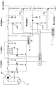
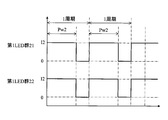
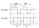
- FIG. 2 is a circuit diagram illustrating an example of a power supply circuit provided in the liquid crystal display device illustrated in FIG. 1. It is a timing chart which shows the lighting state of each LED in case a 1st LED group and a 2nd LED group light simultaneously. It is a timing chart which shows the lighting state of each LED in case a 1st LED group and a 2nd LED group light sequentially. It is a timing chart which shows a sequential lighting state when PWM duty is 50% or more. It is a table
- FIG. 1 is a block diagram of a liquid crystal display device according to the present invention.
- the liquid crystal display device A is a liquid crystal display device capable of displaying a stereoscopic image.
- the liquid crystal display device A includes a liquid crystal panel 1, a light source unit 2, an image signal input unit 3, an image processing circuit 4, a liquid crystal drive circuit 5, a light control circuit 6 (light control means), and a main control circuit 7. (Control means) and a power supply circuit 8 are provided.
- a part of the light source unit 2, the light control circuit 6, the main control circuit 7, and the power supply circuit 8 constitutes a part of the backlight.
- the dotted line is a power supply line
- the solid line is a signal line.
- the liquid crystal panel 1 is filled with liquid crystal between glass substrates arranged in parallel.
- the glass substrate is provided with a transparent electrode made of ITO (Indium Tin Oxide) or the like.
- ITO Indium Tin Oxide
- the liquid crystal panel 1 adjusts the light transmittance of light from a backlight disposed on the back surface, and displays an image on the front surface.
- the light source unit 2 is an illuminating device that is disposed on the back surface of the liquid crystal panel 1 that displays an image and includes a plurality of white LEDs or a plurality of sets of RGB three-color LED chips (hereinafter simply referred to as LEDs) as light sources.
- the backlight is a direct type backlight including a light source unit 2 in which LEDs are two-dimensionally arranged on a surface facing the liquid crystal panel 1.
- the backlight can also adopt an edge light type.
- the light source unit 2 is divided into a first LED group 21 that is a group including a plurality of LEDs, and a second LED group 22 that is also a group including a plurality of LEDs.
- the number of LEDs in the first LED group 21 and the second LED group 22 may be the same or different. Details of the first LED group 21 and the second LED group 22 will be described later.
- the image signal input unit 3 is an interface for inputting an image signal.
- the image processing circuit 4 generates a frame image signal based on the input image signal, and transmits the frame image signal to the liquid crystal driving circuit 5.
- the frame image signal is a signal of image luminance (pixel gradation) of each of the three primary colors (R, G, and B) of each pixel constituting one frame image in the moving image.
- R, G, and B three primary colors
- the liquid crystal driving circuit 5 is a circuit for sequentially displaying on the liquid crystal panel 1 an image for one frame corresponding to the frame image signal based on the frame image signal sequentially transmitted from the image processing circuit 4 at a constant cycle. More specifically, the liquid crystal driving circuit 5 supplies a gradation signal having a voltage corresponding to the pixel gradation included in the frame image signal to the transparent electrode of each pixel provided in the liquid crystal display panel 1. . Thereby, in each pixel of the liquid crystal panel 1, the light transmittance is determined for each pixel, and the light from the light source unit 2 is transmitted, whereby an image is displayed on the front surface of the liquid crystal panel 1.
- the dimming circuit 6 is a circuit for dimming the light source unit 2.
- the lighting of the first LED group 21 and the second LED group 22 is controlled by pulse width modulation (PWM) control (hereinafter referred to as PWM dimming). Details will be described later.
- PWM dimming pulse width modulation
- the main control circuit 7 is a main control unit that controls each circuit of the liquid crystal display device A.
- the main control circuit has a configuration including an arithmetic processing unit such as an MPU, and is connected to a memory 9 that is a storage device including an EEPROM, a ROM, a RAM, and the like.
- the main control circuit 7 receives the luminance signal of the display image from the image processing circuit 4.
- the main control circuit 7 uses a PWM duty (hereinafter referred to as a PWM value) when driving the first LED group 21 and the second LED group 22 based on luminance data included in the luminance signal, and a pulse signal (hereinafter referred to as a PWM value).
- a PWM signal which is referred to as a PWM signal
- a supply current value a timing when the signal is on
- the dimming circuit 6 sends a PWM signal to the first LED group 21 and / or the second LED group 22 based on the PWM value and the supply current value.
- the power supply circuit 8 is a circuit that converts alternating current from the alternating current power supply 800 into direct current.
- the power supply circuit 8 is a circuit that supplies driving (light emission) power to the first LED group 21 and the second LED group 22 of the light source unit 2 and also supplies power to the substrate Bd on which the power supply circuit 8 is mounted. is there.
- Booster circuits 831 and 832 (voltage conversion means) are interposed between the power supply circuit 8 and the first LED group 21 and the second LED group 22.
- the substrate resistance Br is a constant load that does not depend on lighting / extinguishing of the light source unit 2 such as exciting current, iron loss, and copper loss. That is, while the liquid crystal display device A is operating, the substrate Bd consumes constant power (substrate power) due to the substrate resistance Br.
- FIG. 2 is a circuit diagram showing an example of a power supply circuit provided in the liquid crystal display device shown in FIG.
- the power supply circuit 8 includes a rectifier circuit DB connected to an AC power supply 800, a PFC circuit 81 connected to the output side of the rectifier circuit DB, and an LLC connected to the output side of the PFC circuit 81.
- the circuit 82 is connected to each of the first LED group 21 and the second LED group 22 and includes boosting circuits 831 and 832 which are power supply means for boosting the voltage from the LLC circuit 82.
- the PFC circuit 81 and the LLC circuit 82 are conventionally well-known circuits using a coil, a capacitor, a diode, a transformer, a switching element, and the like, and will not be described in detail.
- the pulse signal from the main control circuit 7 is input to the gate of the switching element Q81 (for example, n-type MOSFET) provided in the PFC circuit 81.
- the pulse signal from the main control circuit 7 is input to the gate of the switching element Q82 (for example, n-type MOSFET) provided in the LLC circuit 82.
- the main control circuit 7 outputs direct current (voltage) by switching on and off the switching element Q81 and the switching element Q82 with a pulse signal.
- the booster circuit 831 and the booster circuit 832 are well known booster circuits using coils, capacitors, diodes, and switching elements, and will not be described in detail.
- the booster circuit 831 and the booster circuit 832 are provided with switching elements Q831 and Q832.
- the switching elements Q831 and Q832 are switched by a control signal from the main control circuit 7, thereby boosting the output voltage from the LLC circuit 82 (input voltage to the booster circuits 831 and 832).
- the main control circuit 7 controls the booster circuit 831 and the booster circuit 832 so as to apply to the first LED group 21 and the second LED group 22 a voltage that allows a current necessary for lighting the first LED group 21 and the second LED group 22 to flow.
- the PWM signal is input from the dimming circuit 6 to the switching elements Q21 and Q22 of the first LED group 21 and the second LED group 22.
- the PWM signal input from the dimming circuit 6 is a signal generated based on the PWM value generated by the dimming circuit 6. That is, when the PWM signal is at the H level, the switching elements Q21 and Q22 are turned on, and a current flows through the first LED group 21 and the second LED group 22.
- the light emission luminance of the first LED group 21 and the second LED group 22 is controlled by the PWM value and the current value.
- the power supply circuit 8 supplies power to the light source unit 2 (first LED group 21 and second LED group 22), and the same power supply circuit 8 also supplies power to the electronic components provided on the circuit board. Supply. That is, in the liquid crystal display device A, even when the light source unit 2 is not emitting light, power is consumed by the substrate resistance Br. If the time during which the light source unit 2 is not emitting light is long, the power supply efficiency is lowered.
- the power efficiency of the liquid crystal display device A of the present invention is low based on the load of the light source unit 2 and the PWM value.
- the lighting control is performed so as to increase the power efficiency.
- the light source unit 2 of the liquid crystal display device A includes a first LED group 21 and a second LED group 22, and power is supplied via independent booster circuits 831 and 832, respectively.
- the dimming circuit 6 switches the switching element Q21 of the first LED group 21 and the switching element Q22 of the second LED group 22, thereby controlling the turning on / off of the first LED group 21 and the second LED group 22.
- the first LED group 21 and the second LED are adjusted by adjusting the PWM signal that is input from the dimming circuit 6 to the switching elements Q21 and Q22, in other words, switching the switching elements Q21 and Q22.
- the group 22 can be turned on simultaneously, and the first LED group 21 and the second LED group 22 can be turned on (sequentially turned on) at different lighting timings.
- the case where the first LED group 21 and the second LED group 22 are simultaneously turned on and the case where they are sequentially turned on will be described with reference to the drawings.
- the time when the first LED group 21 and the second LED group 22 are simultaneously lit is referred to as a first lighting mode
- the time when the first LED group 21 and the second LED group 22 are sequentially lit is referred to as a second lighting mode.
- the first lighting mode can suppress the power consumption by the load (luminance) of the light source unit 2 and
- the second lighting mode is divided into a case where power consumption can be suppressed. Therefore, in the liquid crystal display device A of the present invention, the power consumption is suppressed by lighting the light source unit 2 in either the first lighting mode or the second lighting mode.
- switching between the first lighting mode and the second lighting mode will be described. It is assumed that the first LED group 21 and the second LED group 22 are controlled with the same current value and the same PWM value.
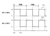
- FIG. 3 is a timing chart showing the lighting state of each LED when the first LED group and the second LED group included in the liquid crystal display device according to the present invention are lit simultaneously.
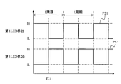
- FIG. 4 shows the liquid crystal display device according to the present invention. It is a timing chart which shows the lighting state of each LED in case the 1st LED group and 2nd LED group which are included light up sequentially.
- the timing charts shown in FIGS. 3 and 4 show PWM signals for turning on / off the switching element Q21 and the switching element Q22. The PWM value is expressed in%.
- the PWM value of the first LED group 21 and the second LED group 22 is 50%, that is, the lighting period of each LED group 21 and 22 in one cycle. 50%.
- the PWM signals P11 and P12 input to the switching element Q21 and the switching element Q22 have the same timing T11. Becomes H level (rise), and becomes L level (falls) at the same timing T12. Accordingly, in the light source unit 2, the first LED group 21 and the second LED group 22 are repeatedly turned on / off simultaneously.
- the PWM signal P21 for switching the switching element Q21 is at the H level in the first half of the period (period).
- the PWM signal P22 for switching the switching element Q22 is at the L level.
- the PWM signal P21 changes from the H level to the L level at the intermediate period T21.
- the PWM signal P22 changes from the L level to the H level. That is, in the second lighting mode, in the first half of the cycle, the switching element Q21 is on and the switching element Q22 is off, and in the second half, the switching element Q22 is on when the switching element Q21 is off.
- the dimming circuit 6 outputs a PWM signal as shown in FIG. 4 to each of the switching element Q21 and the switching element Q22, so that the first LED group 21 is turned on and the second LED group 22 is turned off in the first half of the cycle. . Conversely, in the second half of the cycle, the first LED group 21 is turned off and the second LED group 22 is turned on. Thus, when the light source unit 2 is driven in the second lighting mode, the time during which the LEDs are completely turned off can be eliminated.
- the load calculation formula differs depending on whether the PWM value is 50% or more and less than 50%. Therefore, in the following description, it will be described separately when the PWM value is less than 50% and when the PWM value is 50% or more.
- the load of the first LED group 21, the second LED group 22, and the substrate resistance Br, the booster circuit, and the power supply efficiency of the LLC circuit are as follows.
- ⁇ power supply efficiency of the booster circuits 831 and 832 connected to each LED at the moment when current flows (lights) in the first LED group 21 and the second LED group 22.
- ⁇ The power supply efficiency of the LLC circuit at the moment when current flows through both LED groups simultaneously.
- ⁇ The power supply efficiency of the LLC circuit at the moment when the current flows only in one LED group.
- ⁇ Power supply efficiency of the LLC circuit at the moment when no current flows through both LED groups.
- Don PWM value (ratio in which the PWM signal is at the H level). Note that ⁇ , ⁇ , ⁇ , ⁇ , and Don are expressed as percentages (%). In the following formula, all are divided by 100, that is, a small number between 0 and 1. To do.
- the load W1 in the first lighting mode is obtained as follows.
- the power supply efficiency of the booster circuits 831 and 832 is ⁇ . Therefore, the first LED group 21 and the second LED group 22 The load is (2 ⁇ Pa / ⁇ ).
- the first LED group 21 and the second LED group 22 are lit simultaneously, power is supplied to the first LED group 21, the second LED group 22, and the substrate resistance Br.
- the load at the time of simultaneous lighting is ⁇ (Pb + 2 ⁇ Pa / ⁇ ) / ⁇ .
- the efficiency of the LLC circuit at the moment when electric power is supplied only to the substrate resistance Br and no current flows through both the LED groups 21 and 22 (lights out simultaneously) is ⁇ . From this, the load when the current is not supplied to both the LED groups 21 and 22 is (Pb / ⁇ ).
- the rate at which the first LED group 21 and the second LED group 22 are simultaneously turned on in one cycle is Don, and the rate at which they are simultaneously turned off is 1-Don. From this, the load W1 in the first lighting mode is expressed by the following mathematical formula.
- the load W2 in the second lighting mode is obtained as follows.
- the load when the first LED group 21 is turned on and the second LED group 22 is turned off is that the efficiency of the LLC circuit at the moment when one LED group is turned on is ⁇ , so that (Pb + Pa / ⁇ ) / ⁇ Become.
- the load when the second LED group 22 is lit is the same load. That is, in the second lighting mode, the load for a period twice that of Don is (Pb + Pa / ⁇ ) / ⁇ .
- the load during the period when the first LED group 21 and the second LED group 22 are simultaneously turned off is the same as described above. That is, Pb / ⁇ , and the ratio of the period during which the first LED group 21 and the second LED group 22 are simultaneously turned off is (1-2 ⁇ Don). From the above, the load W2 in the second lighting mode is expressed by the following equation.
- the driving in the second lighting mode can reduce the load and suppress power consumption. Can do. That is, the conditional expression that gives the switching condition between the first lighting mode and the second lighting mode is as follows. When this formula is arranged, the following formula is obtained.
- the load W2 when the light source unit 2 is lit in the second lighting mode is smaller than the load W1 when the light source unit 2 is lit in the first lighting mode. Become. Therefore, when the PWM value is less than 50% and the condition 1 is satisfied, the light source unit 2 is controlled to be turned on in the second lighting mode, and when the condition 1 is not satisfied, the light source unit 2 is turned on in the first lighting mode. Thus, the power consumption of the liquid crystal display device A can be suppressed.
- the first LED group 21, the second LED group 22, the load of the substrate resistance, and the power efficiency under each condition are the same as when the PWM value is less than 50%, and the same reference numerals are used.
- the first lighting mode is the same as when the PWM value is less than 50%, and the details are omitted.
- the load W3 in the first lighting mode is expressed by the following formula.
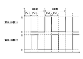
- FIG. 5 is a timing chart showing a sequential lighting state when the PWM duty is 50% or more.
- the lighting period of the light source unit 2 will be described by dividing it into three. That is, only the first period St1 in which only the first LED group 21 in the first half of the period is lit, the second period St2 in which the first LED group 21 and the second LED group 22 in the middle stage are lit, and only the second LED group 22 in the second half.
- the third period St3 is on.
- the load W4 in the second lighting mode is calculated as follows. In the first period St1, only the first LED group 21 is lit, and the load at this time is (Pb + Pa / ⁇ ) / ⁇ . Since the loads of the first LED group 21 and the second LED group 22 are the same, the loads during the third period St3 are also the same. Further, since the first period St1 is a period in which the second LED group 22 is turned off in one period, the ratio of the first period St1 in one period is (1-Don). Since the PWM values of the first LED group 21 and the second LED group 22 are the same, the ratio of the third period St3 within one cycle is the same (1-Don).
- the first LED group 21 and the second LED group 22 are turned on simultaneously, and the load at this time is ⁇ (Pb + 2 ⁇ Pa / ⁇ ) / ⁇ .
- the second period St2 is when the PWM signals are simultaneously at the H level within one cycle, and the ratio of the second period St2 within one cycle is (2 ⁇ Don ⁇ 1). From the above, the load W4 in the second lighting mode is expressed by the following equation.
- the load W4 when the light source unit 2 is lit in the second lighting mode is smaller than the load W3 when the light source unit 2 is lit in the first lighting mode. Become. From this, when the PWM value is 50% or more and the condition 2 is satisfied, the light source unit 2 is controlled to be lit in the second lighting mode, and when the condition 2 is not satisfied, the light source unit 2 is lit in the first lighting mode.
- the PWM value is 50% or more, the power consumption of the liquid crystal display device A can be suppressed.
- Condition 1 and condition 2 are the same expression, and whether or not condition 1 (that is, condition 2) is satisfied regardless of the PWM value is a switching condition for switching between the first lighting mode and the second lighting mode. .
- lighting control is performed by selecting either the first lighting mode or the second lighting mode depending on whether or not the switching condition (condition 1) is satisfied.
- the lighting mode may be selected by the dimming circuit 6 or the main control circuit 7.
- the dimming circuit 6 When performing in the main control circuit 7, information indicating whether any lighting mode is selected is transmitted to the dimming circuit 6 depending on whether the condition 1 is satisfied.
- the dimming circuit 6 that has received the information on the selected lighting mode transmits a PWM signal to the switching circuits Q21 and Q22 so that the first LED group 21 and the second LED group 22 are lit in the selected lighting mode.
- FIG. 6 is a table showing lighting conditions of the light source unit. In order to calculate the load, a description will be given separately for low luminance (PWM value 45%) and high luminance (PWM value 65%).
- Example 1 In the case of low luminance, each value shown in FIG. 6 is considered as a switching condition.
- H1 75.3 (%).
- ⁇ 60 (%) and the condition 1 is satisfied.
- the power consumption can be reduced by driving the light source unit 2 in the second lighting mode.
- the load W1 when the first lighting mode is turned on under the conditions shown in FIG. 6 is about 34.3 (W), and the load W2 when turned on in the second lighting mode is about 31.25 (W). By turning on the light source unit 2 in the lighting mode, power of about 3.05 (W) can be reduced.
- the load W3 when lighting in the first mode under the conditions shown in FIG. 6 is approximately 34.73 (W)
- the load W4 when lighting in the second lighting mode is approximately 32.36 (W).
- Example 2 Considering each value shown in FIG. 6 as a switching condition.
- H1 75.3 (%).
- the load W1 when the first lighting mode is turned on under the conditions shown in FIG. 6 is approximately 29.72 (W)
- the load W2 when the second lighting mode is turned on is approximately 30.42 (W).
- about 0.7 (W) of power can be reduced by lighting the light source unit 2 in the first lighting mode.
- the PWM value is 65% ( ⁇ 50%). Therefore, the load W3 when the first mode is turned on under the conditions shown in FIG. 6 is approximately 31.81 (W), and the light is turned on in the second lighting mode. The load W4 at that time is approximately 32.35 (W), and by turning on the light source unit 2 in the second lighting mode, power of about 0.54 (W) can be reduced.
- the liquid crystal display device A of the present invention reduces power consumption by switching the lighting control of the light source unit 2 based on the load of the light source unit, the load due to the substrate resistance, and the value of the power supply efficiency. .
- the lighting mode may be confirmed every certain time, or the switching condition is confirmed at the timing when the current supplied to the LED is changed, and the lighting mode is selected as necessary. May be changed.
- the light source unit 2 having two channels has been described, but the present invention is not limited to this, and the light source unit 2 having more channels.
- a drive mode that can reduce power consumption can be selected by the same method.
- FIG. 7 is a block diagram of another example of the liquid crystal display device according to the present invention
- FIG. 8 is a circuit diagram of a power supply circuit of the liquid crystal display device shown in FIG.
- the power supply circuit 8 ⁇ / b> B of the liquid crystal display device B is configured to boost the voltage supplied to the first LED group 21 and the second LED group 22 with one booster circuit 831.
- the same configuration as the power supply circuit 8 has the same configuration as the power supply circuit 8, and the same reference numerals are given to substantially the same configuration.
- one of the first LED group 21 or the second LED group 22 is The power supply efficiency of the booster circuit 831 changes between when the LED is lit and when the first LED group 21 and the second LED group 22 are driven. That is, unlike the power supply circuit 8 including two booster circuits, it is necessary to determine a switching condition in consideration of a change in power supply efficiency of the booster circuit 831 depending on the number of lighting LEDs.
- the PWM value is less than 50%.
- the load W21 when the first LED group 21 and the second LED group 22 are driven in the first lighting mode is expressed by the following equation.
- the load W22 when the first LED group 21 and the second LED group 22 are driven in the second lighting mode is represented by the following expression.
- the condition that satisfies W21> W22 is expressed by the following equation.
- the load W22 when the light source unit 2 is lit in the second lighting mode is smaller than the load W21 when the light source unit 2 is lit in the first lighting mode.
- the PWM value is less than 50% and the condition 3 is satisfied
- the light source unit 2 is controlled to be lit in the second lighting mode, and when the condition 3 is not satisfied, the light source unit 2 is lit in the first lighting mode.
- the power consumption of the liquid crystal display device B can be suppressed.
- the load W23 when the first LED group 21 and the second LED group 22 are driven in the first lighting mode is expressed by the following equation.
- the load W24 when the first LED group 21 and the second LED group 22 are driven in the second lighting mode is expressed by the following equation.
- the condition that satisfies W23> W24 is expressed by the following equation.
- the load W4 when the light source unit 2 is lit in the second lighting mode is smaller than the load W3 when the light source unit 2 is lit in the first lighting mode. Become. From this, when the PWM value is 50% or more and the condition 4 is satisfied, the light source unit 2 is controlled to be turned on in the second lighting mode, and when the condition 4 is not satisfied, the light source unit 2 is turned on in the first lighting mode.
- the PWM value is 50% or more, the power consumption of the liquid crystal display device B can be suppressed.
- Condition 3 and condition 4 are the same expression, and whether or not condition 3 (that is, condition 4) is satisfied regardless of the PWM value is a switching condition for switching between the first lighting mode and the second lighting mode. . That is, in the liquid crystal display device B, the lighting control of the light source unit 2 is performed by selecting either the first lighting mode or the second lighting mode depending on whether the switching condition (condition 3) is satisfied.
- the power consumption is reduced. Can be reduced.
- FIG. 9 is a block diagram of another example of the liquid crystal display device according to the present invention
- FIG. 10 is a timing chart showing lighting states of the first LED group and the second LED group of the liquid crystal display device shown in FIG.
- the liquid crystal display device C shown in FIG. 9 has the same configuration as the liquid crystal display device A except that the main control circuit 7c is different, and substantially the same parts are denoted by the same reference numerals and description of the same parts is omitted. .
- the main control circuit 7c of the liquid crystal display device C shown in FIG. 9 is more optimal than the lighting mode in which the PWM value and the current value are changed. Select a lighting mode with less power.
- selection of the lighting mode by the liquid crystal display device C will be described with reference to the drawings.
- 10A, 10B, 10C, and 10D are timing charts of lighting modes in which the first LED group and the second LED group included in the liquid crystal display device illustrated in FIG. 9 are lit.
- the vertical axis represents current value
- the horizontal axis represents time.
- the main control circuit 7c based on the luminance of the first LED group 21 and the second LED group 22, supplies a plurality (here, two types) of supply current values I1 and I2 and PWM values corresponding to the supply current values I1 and I2. Pw1 and Pw2 are determined. Note that a method of determining the supply current value with respect to the luminance with reference to a lookup table provided in the memory 9 can be employed.
- the supply current value determined by the main control circuit 7c is I1> I2. If the brightness of the LED groups 21 and 22 is the same, the PWM value is inevitably Pw1 ⁇ Pw2 due to the condition of the supply current value. Note that Pw2 is 50% or more. In addition, since the electric resistance of the first LED group 21 and the second LED group 22 is constant, in order to achieve the supply current value, the voltage applied from the booster circuits 831 and 832 to the first LED group 21 and the second LED group 22. The value is also determined. When the supply current value is I1> I2, the voltage value applied to the first LED group 21 and the second LED group 22 is V1> V2.
- the power supply efficiency of the booster circuits 831 and 832 varies depending on the output voltage value.
- the booster circuits 831 and 832 are configured such that the power supply efficiency increases as the output voltage increases in order to increase the stability and efficiency at high loads, and the power supply efficiency ⁇ is ⁇ 31 and voltage value V2 when the voltage value is V1. If ⁇ 32 in this case, the relationship of ⁇ 31> ⁇ 32 holds.
- the drive mode when the PWM value is Pw1 (less than 50%) is as shown in FIGS. 10A and 10B. That is, the first LED group 21 and the second LED group 22 are driven by the supply current I1 and the PWM value Pw1. As shown in FIG. 10B, there is a period in which the first LED group 22 is not driven when driven in the second lighting mode.
- the load W31 in the first lighting mode and the load W32 in the second lighting mode when the PWM value is Pw1 are expressed by the following equations, respectively.
- the drive mode when the PWM value is Pw2 (50% or more) is as shown in FIGS. 10C and 10D. That is, the first LED group 21 and the second LED group 22 are driven by the supply current I2 and the PWM value Pw2. As shown in FIG. 10C, when driving in the second lighting mode, there is a period in which the first LED group 22 is driven simultaneously.
- the load W33 in the first lighting mode and the load W34 in the second lighting mode when the PWM value is Pw2 are represented by the following equations, respectively.
- the main control circuit 7c changes the PWM value and the current value from the above formulas, and compares the loads W31, W32, W33 and W34 when driven in both the first lighting mode and the second lighting mode.
- the main control circuit 7c determines the PWM value, current value, and lighting mode when the load value is the lowest, and sends the information to the dimming circuit 6. Based on the information, the dimming circuit 6 transmits signals for driving the first LED group 21, the second LED group 22, and the booster circuits 831 and 832.
- the lighting control for switching the lighting mode of the LED group is performed by the load of the light source unit 2. As a result, the power consumption of the liquid crystal display device C can be reduced.
- the liquid crystal display device C has a configuration in which the light source unit 2 includes two groups (two channels) of LED groups and supplies power to each of the LED groups 21 and 22.
- the system includes a group of LED groups, and switching between the first lighting mode in which each LED group is simultaneously turned on / off or the second lighting mode in which the LED groups are sequentially lit is determined by the power consumed by the LED group (LED load). As a result, the power consumption of the liquid crystal display device C can be reduced.
- the present invention is not limited to this, and the power supply efficiency of the booster circuits 831 and 832 varies depending on the supply current value.
- the PWM value and calculating the load it is possible to drive in the PWM value and lighting mode that can reduce the supply current, and it is possible to obtain a further energy saving effect.
- the two lighting modes are switched and the LED group is lit and driven.However, assuming more lighting modes, the load in each mode is calculated and compared, An optimal lighting mode may be determined. By selecting from a larger number of lighting modes, it is possible to suppress a change in luminance and enhance the power consumption reduction effect of the liquid crystal display device.
- the output voltage from the LLC circuit 82 is boosted and supplied using the booster circuits 831 and 832 as voltage conversion means.
- the structure provided with a circuit may be sufficient.
- it may be configured to include both a step-up / step-down circuit that supports both step-up and step-down and steps up or down the output voltage as necessary.
- the present invention can be used as a display device for devices such as a thin television device, a thin display device, and a mobile phone.
Landscapes
- Control Of Indicators Other Than Cathode Ray Tubes (AREA)
- Liquid Crystal Display Device Control (AREA)
- Liquid Crystal (AREA)
Abstract
輝度を精度良く調整することができるとともに、消費電力を低減するため、複数系統のLED群21、22を同時に点灯、同時に消灯する同時点灯モードと、複数のLED群21、22の点灯開始タイミングをずらし、順次点灯する順次点灯モードのうち、全体の負荷が低くなる点灯モードを選択し、選択した点灯モードに基づいて調光手段6を制御する制御手段7を備えたバックライト。
Description
本発明は、LEDを光源として液晶パネルに面状光を照射するバックライトを備えた液晶表示装置に関するものである。
液晶表示装置において、LEDを光源に用いるバックライトが採用されることが増えている。前記バックライトでは、パルス幅変調(PWM)制御にてLEDの点灯時間を制御しており(以下、PWM調光と称する場合がある)、低電力での低輝度点灯を実現している。
また、液晶表示装置の電源回路の負荷は、前記LEDの消費電力と、基板(回路系)電力の負荷の2つに大別される。前記基板には前記LEDと共通の電源より電力が供給されるため、前記基板電力は前記LEDの消費電力の変動による電源効率の悪化の要因となる。例えば、PWM調光におけるデューティ値(以下、PWM値と称する場合がある)が0のとき、すなわち、前記LEDが消灯している瞬間(バックライトオフ期間)は、バックライトでの消費電力は、前記基板電力のみとなり、電源効率が悪く、電力損失が増加する。また、デューティ値を変えずに、LEDに供給する電流値を調整してLEDの輝度を調整する制御(以下、電流調光と称する場合がある)でも同様の問題点を有している。
すなわち、液晶表示装置のバックライトでは、低輝度時の電源効率が、高輝度時に比べ、大幅に悪化する。このことが、液晶表示装置全体としての消費電力の増加の原因となっている。
このような、バックライトオフ期間の電源効率の低下を抑制するため、特開2010-60746号公報に記載の液晶表示装置では、中間輝度で調光を行う場合において、必要輝度に応じた必要最小限の電流値でPWM調光を行うことで、消費電力の低減を図っている。特開2010-60746号公報の発明では、電流値を必要最小限とすることで、PWM値を高くし、バックライトオフ期間を短くして電源効率の悪化を抑制し、消費電力の低減、すなわち、省エネルギ化を図っている。
LEDは必要輝度が決まると、供給される電流値の最小値も決まる特性を有している。特開2010-60746号公報の液晶表示装置では、最小電流値でPWM調光を行っているので、バックライトをさらに低輝度で発光させる場合、LEDへの電流値を下げることができず、PWM制御で用いるPWM信号がオフ、すなわち、バックライトオフ期間を長くしなくてはならない。LEDのオフ期間が長くなることで、電源効率が悪化し、消費電力が多くなる。
そこで本発明は、輝度を精度良く調整することができるとともに、消費電力を低減することができるバックライト及びそのバックライトを利用した液晶表示装置を提供することを目的とする。
上記目的を達成するために本発明は、系統ごとに所定数のLED素子が接続された複数系統のLED群と、PWM制御にて前記各LED群に供給される電力を調整し前記LED群の輝度の制御を行う調光手段と、前記LED群の輝度にあわせて前記調光手段を制御する制御手段と、前記LED群を含む各手段に電力を供給する電力供給手段とを備えており、 前記制御手段は、前記複数系統のLED群を同時に点灯、同時に消灯する同時点灯モードと、前記複数系統のLED群の点灯開始タイミングをずらし、順次点灯する順次点灯モードのうち、全体の負荷が低くなる点灯モードを選択し、選択した点灯モードに基づいて前記調光手段を制御するバックライトを提供する。
この構成によると、前記LED群の点灯時の負荷によって、最適な点灯モードで前記各LED群の点灯制御を行うことで、電力供給手段の電源効率が低下するのを抑制することができる。これにより、電源効率の低下で発生する無駄な電力消費を抑えることができ、それだけ、省エネルギ化することが可能である。また、点灯モードが変化しても、バックライトからの輝度は変化しないので、輝度を変化させることなく、省エネルギ化が可能であるともいえる。
上記構成において、前記順次点灯モードは、前記複数のLED群の全てが同時に消灯している期間が発生しない又は短くなるように各LED群の点灯開始タイミングを有していてもよい。
上記構成において、前記調光手段は、PWMデューティを変化させて、前記LED群の輝度を調整していてもよい。
上記構成において、前記調光手段は、前記LED群を点灯させるときに供給する電流レベルを変化させて、前記LED群の輝度を調整していてもよい。
上記構成において、前記調光手段は、PWMデューティと電流レベルとを変化させて、前記LED群の輝度を調整していてもよい。
上記構成において、前記同時点灯モード及び前記順次点灯モードは、電流レベルごとに設けられており、前記制御手段が、負荷が最も小さくなる電流レベル及び点灯モードを選択してもよい。
上記構成において、前記電力供給手段が、前記LED群それぞれと個別に接続し、入力電圧を前記LED群に供給される電力に対応する電圧に変換して出力する電圧変換手段を備えていてもよい。
上記構成において、前記電力供給手段が、前記複数のLED群のうち少なくとも2以上の系統のLED群と接続し、入力電圧を前記LED群に供給される電力に対応する電圧に変換して出力する電圧変換手段を備えていてもよい。
上記構成において、前記調光手段は、前記LED群に備えられているスイッチング素子をスイッチングすることで前記LED群の輝度を制御してもよい。
上記構成のバックライトを利用するものとして、前記バックライトの前面に配置された液晶パネルを備えた液晶表示装置を挙げることができる。
本発明によると、輝度を精度良く調整することができるとともに、消費電力を低減することができるバックライト及びそのバックライトを利用した液晶表示装置を提供することができる。
以下に本発明の実施形態について図面を参照して説明する。
(第1の実施形態)
以下に本発明の実施形態について図面を参照して説明する。図1は本発明にかかる液晶表示装置のブロック図である。図1に示すように、液晶表示装置Aは、立体画像を表示することが可能な液晶表示装置である。液晶表示装置Aは、液晶パネル1と、光源ユニット2と、画像信号入力部3と、画像処理回路4と、液晶駆動回路5と、調光回路6(調光手段)と、メイン制御回路7(制御手段)と、電源回路8とを備えている。光源ユニット2、調光回路6、メイン制御回路7及び電源回路8の一部(後述する昇圧回路)はバックライトの一部を構成している。なお、図1に示す液晶表示装置Aにおいて、点線は電力の供給線であり、実線は信号線である。
以下に本発明の実施形態について図面を参照して説明する。図1は本発明にかかる液晶表示装置のブロック図である。図1に示すように、液晶表示装置Aは、立体画像を表示することが可能な液晶表示装置である。液晶表示装置Aは、液晶パネル1と、光源ユニット2と、画像信号入力部3と、画像処理回路4と、液晶駆動回路5と、調光回路6(調光手段)と、メイン制御回路7(制御手段)と、電源回路8とを備えている。光源ユニット2、調光回路6、メイン制御回路7及び電源回路8の一部(後述する昇圧回路)はバックライトの一部を構成している。なお、図1に示す液晶表示装置Aにおいて、点線は電力の供給線であり、実線は信号線である。
液晶パネル1は、平行に配置されたガラス基板の間に液晶が充填されている。ガラス基板にはITO(Indium Tin Oxide)等で形成された透明電極が備えられており、透明電極を利用して液晶に電圧を印加することで、液晶パネル1に入射される光の光透過率が調整される。液晶パネル1は背面に配置されたバックライトからの光の光透過率を調整し、前面に画像を表示する。
光源ユニット2は、画像を表示する液晶パネル1の背面に配置され、光源として複数個の白色LED又は複数組のRGB3色のLEDチップ(以下、単にLEDと称する)を備えた照明装置である。なお、液晶表示装置Aにおいて、バックライトは、液晶パネル1と対向する面にLEDが2次元配列された光源ユニット2を備えた直下式バックライトである。また、バックライトは、直下式以外にもエッジライト式を採用することも可能である。また、光源ユニット2は、複数個のLEDを含むグループである第1LED群21と、同じく複数個のLEDを含むグループである第2LED群22とに分けられている。なお、第1LED群21と第2LED群22のLED数は同じであってもよいし、異なっていてもよい。第1LED群21及び第2LED群22の詳細については、後述する。
画像信号入力部3は、画像信号を入力するインターフェースである。画像処理回路4は、入力された画像信号に基づいて、フレーム画像信号を生成し、そのフレーム画像信号を液晶駆動回路5に伝送する。なお、フレーム画像信号は、ここでは、動画における1フレームの画像を構成する各画素の3原色(R、G、B)それぞれの画像輝度(画素階調)の信号である。また、動画を表示する場合、フレーム画像信号は順次生成されそのつど液晶駆動回路5に伝送される。また、画像処理回路4は、画像信号に基づいて、光源ユニット2より出射される面状光の輝度を示す輝度信号を生成し、メイン制御回路7に送信する。
液晶駆動回路5は、画像処理回路4から一定周期で順次伝送されてくるフレーム画像信号に基づいて、そのフレーム画像信号に対応する1フレーム分の画像を液晶パネル1に順次表示させる回路である。具体的に説明すると、液晶駆動回路5は、液晶表示パネル1に設けられた各画素の透明電極に対し、フレーム画像信号に含まれる画素階調に応じた電圧の階調信号を供給している。これにより、液晶パネル1の各画素では、画素毎に光の光透過率が決定され、光源ユニット2からの光が透過することで、液晶パネル1の前面に画像が表示される。
調光回路6は、光源ユニット2を調光する回路である。パルス幅変調(PWM)制御にて第1LED群21及び第2LED群22の点灯を制御している(以下、PWM調光と称する)。詳細については、後述する。
メイン制御回路7は、液晶表示装置Aの各回路の制御を行う主制御部である。メイン制御回路は、MPU等の演算処理装置を含む構成を有しており、EEPROM、ROM、RAM等を含む記憶装置であるメモリ9と接続されている。メイン制御回路7は、画像処理回路4から表示画像の輝度信号を受け取る。メイン制御回路7は、輝度信号に含まれる輝度データに基づいて第1LED群21及び第2LED群22を駆動するときのPWMデューティ(以下、PWM値と称する)及びPWM値に基づいたパルス信号(以下、PWM信号と称する)がオンのタイミングで供給する電流値(以下、供給電流値と称する場合がある)を決定し、PWM値及び供給電流値を調光回路6に送る。調光回路6は、PWM値及び供給電流値に基づいて、PWM信号を第1LED群21及び(又は)第2LED群22に送出する。
電源回路8は、交流電源800からの交流を直流に変換する回路である。なお、電源回路8は、光源ユニット2の第1LED群21及び第2LED群22に駆動(発光)電力を供給しているとともに、電源回路8が実装されている基板Bdに電力を供給する回路でもある。電源回路8と第1LED群21及び第2LED群22との間には昇圧回路831、832(電圧変換手段)が介在している。なお、基板Bdには液晶表示装置Aが動作している間、常に電力が供給されており基板抵抗Brが存在している。基板抵抗Brは励磁電流、鉄損、銅損等の光源ユニット2の点灯/消灯に依存しない、一定の負荷である。すなわち、液晶表示装置Aが動作している間、基板Bdでは基板抵抗Brによる一定の電力(基板電力)が消費される。
次に、LEDに電力を供給する回路について説明する。図2は図1に示す液晶表示装置に備えられた電源回路の一例を示す回路図である。図2に示すように、電源回路8は、交流電源800に接続された整流回路DBと、整流回路DBの出力側に接続されたPFC回路81と、PFC回路81の出力側に接続されたLLC回路82と、第1LED群21及び第2LED群22それぞれと接続し、LLC回路82からの電圧を昇圧する電力供給手段である昇圧回路831、832とを備えている。
PFC回路81及びLLC回路82は、コイル、キャパシタ、ダイオード、トランス、スイッチング素子等を用いた、従来よく知られた回路であり詳細な説明は省略する。PFC回路81に備えられたスイッチング素子Q81(例えば、n型MOSFET)のゲートには、メイン制御回路7からのパルス信号が入力されている。また、LLC回路82に備えられたスイッチング素子Q82(例えば、n型MOSFET)のゲートには、メイン制御回路7からのパルス信号が入力されている。メイン制御回路7は、パルス信号でスイッチング素子Q81及びスイッチング素子Q82のオンオフを切り換えることで、直流(電圧)を出力している。
昇圧回路831及び昇圧回路832もコイル、キャパシタ、ダイオード及びスイッチング素子を用いた従来よく知られた昇圧回路であり、詳細な説明は省略する。昇圧回路831及び昇圧回路832には、スイッチング素子Q831、Q832が備えられている。スイッチング素子Q831、Q832はメイン制御回路7からの制御信号によってスイッチング操作されており、これにより、LLC回路82からの出力電圧(昇圧回路831、832への入力電圧)を昇圧している。
メイン制御回路7は、第1LED群21及び第2LED群22の点灯に必要な電流を流せる電圧を第1LED群21及び第2LED群22に印加するように、昇圧回路831及び昇圧回路832を制御する。さらに、第1LED群21、第2LED群22のスイッチング素子Q21、Q22には、調光回路6からPWM信号が入力されている。調光回路6から入力されるPWM信号は、調光回路6で生成されたPWM値に基づいて生成された信号である。すなわち、PWM信号がHレベルのとき、スイッチング素子Q21、Q22はオンになり、第1LED群21、第2LED群22に電流が流れる。以上のようにして、第1LED群21及び第2LED群22は、PWM値と電流値で発光輝度が制御されている。
次に本発明にかかる液晶表示装置のPWM調光について説明する。液晶表示装置Aでは、電源回路8で、光源ユニット2(第1LED群21、第2LED群22)に電力を供給しているとともに、同じ電源回路8で回路基板に備えられた電子部品にも電力を供給している。つまり、液晶表示装置Aでは光源ユニット2が発光していないときも基板抵抗Brによって電力が消費されており、光源ユニット2が発光していない時間が長いと電源効率が低下する。
このような液晶表示装置Aにおいて、光源ユニット2の負荷が低いときの電源効率を改善するため、本発明の液晶表示装置Aでは、光源ユニット2の負荷とPWM値に基づいて、電源効率が低いとき、光源ユニット2が発光していない時間を減らし、電源効率を高めるように点灯制御を行っている。
本発明にかかる液晶表示装置の光源ユニットの点灯制御について図面を参照して説明する。図2に示すように、液晶表示装置Aの光源ユニット2は、第1LED群21と第2LED群22とを備えており、それぞれ、独立した昇圧回路831、832を介して電力が供給されている。そして、調光回路6が第1LED群21のスイッチング素子Q21、第2LED群22のスイッチング素子Q22をスイッチングすることで、第1LED群21及び第2LED群22の点灯/消灯を制御している。
光源ユニット2の点灯を行う場合、調光回路6から各スイッチング素子Q21、Q22に入力する、換言すると、スイッチング素子Q21、Q22をスイッチングするPWM信号を調整することで、第1LED群21及び第2LED群22を同時点灯することも可能であり、第1LED群21と第2LED群22の点灯タイミングをずらして点灯(順次点灯)することも可能である。以下に、第1LED群21と第2LED群22が同時点灯する場合と順次点灯する場合に分けて図面を参照して説明する。また、第1LED群21及び第2LED群22が同時点灯するときを第1点灯モード、順次点灯するときを第2点灯モード称する。
液晶表示装置Aでは、基板抵抗Brが光源ユニット2の負荷にかかわらず一定であるので、光源ユニット2の負荷(輝度)によって、第1点灯モードの方が消費電力を抑えることができる場合と、第2点灯モードの方が消費電力を抑えることができる場合とに分けられる。そこで、本発明の液晶表示装置Aでは、光源ユニット2を第1点灯モード又は第2点灯モードのいずれか適切な点灯モードで点灯することで消費電力を抑えている。次に、第1点灯モードと第2点灯モードとの切り替えについて説明する。なお、第1LED群21及び第2LED群22は同じ電流値、同じPWM値で制御されているものとする。
図3は本発明にかかる液晶表示装置に含まれる第1LED群と第2LED群とが同時点灯する場合の各LEDの点灯状態を示すタイミングチャートであり、図4は本発明にかかる液晶表示装置に含まれる第1LED群と第2LED群とが順次点灯する場合の各LEDの点灯状態を示すタイミングチャートである。図3、図4に示すタイミングチャートは、スイッチング素子Q21、スイッチング素子Q22をオン/オフするPWM信号を示している。なお、PWM値は%で表示し、図3、図4では、第1LED群21、第2LED群22のPWM値が50%、すなわち、1周期での各LED群21、22の点灯の期間が50%である。
図3に示すように、第1LED群21と第2LED群22とが同時点灯(第1点灯モード)のとき、スイッチング素子Q21及びスイッチング素子Q22に入力されるPWM信号P11、P12は、同じタイミングT11でHレベルになり(立ち上がり)、同じタイミングT12でLレベルになる(立ち下がる)。これにより、光源ユニット2は、第1LED群21と第2LED群22とが同時に点灯/消灯を繰り返す。
図4に示すように、第2点灯モードのとき、スイッチング素子Q21をスイッチングするPWM信号P21は周期(期間)の前半でHレベルである。このとき、スイッチング素子Q22をスイッチングするPWM信号P22はLレベルである。周期の中間T21でPWM信号P21はHレベルからLレベルに変わる。これと同時にPWM信号P22はLレベルからHレベルに変わる。すなわち、第2点灯モードのとき、周期の前半では、スイッチング素子Q21がオンでスイッチング素子Q22がオフになり、後半では、スイッチング素子Q21がオフのときスイッチング素子Q22がオンになっている。
つまり、調光回路6が、図4に示すようなPWM信号をスイッチング素子Q21、スイッチング素子Q22のそれぞれに出力することで、周期の前半で第1LED群21が点灯し第2LED群22が消灯する。逆に、周期の後半では、第1LED群21が消灯し第2LED群22が点灯する。このように、光源ユニット2を第2点灯モードで駆動する場合、LEDが完全に消灯している時間をなくすことができる。なお、第2点灯モードにおいてPWM値が50%未満の場合、PWM信号をずらしても第1LED群21及び第2LED群22の両方が点灯しない期間が発生し、PWM値が50%を超えると、第1LED群21及び第2LED群22が同時に点灯する期間が発生する。
以下に、第1点灯モードと第2点灯モードのいずれを選択するかの条件について説明する。まず、光源ユニット2を第2点灯モードで駆動する場合について説明する。第2点灯モードではWM値が50%未満のとき、第1LED群21及び第2LED群22が同時にオフになる期間が発生する。つまり、PWM値が50%以上か50%未満かで負荷の計算式が異なる。そのため、以下の説明では、PWM値が50%未満のときと、50%以上のときに分けて説明する。なお、第1LED群21及び第2LED群22及び基板抵抗Brの負荷及び昇圧回路、LLC回路の電源効率は次のとおりである。
Pa(W) :第1LED群21、第2LED群22の負荷。
Pb(W) :基板抵抗Brによる負荷。
γ :第1LED群21、第2LED群22に電流が流れている(点灯している)瞬間の各LEDに接続された昇圧回路831、832の電源効率。
α :両方のLED群に同時に電流が流れている瞬間のLLC回路の電源効率。
β :片方のLED群だけに電流が流れている瞬間のLLC回路の電源効率。
η :両方のLED群に電流が流れていない瞬間のLLC回路の電源効率。
Don :PWM値(PWM信号がHレベルである割合)。
なお、α、β、γ、η及びDonは百分率(%)で表されるものであるが、以下の式では、全て、100で除したもの、すなわち、0~1の間の少数であるとする。
Pa(W) :第1LED群21、第2LED群22の負荷。
Pb(W) :基板抵抗Brによる負荷。
γ :第1LED群21、第2LED群22に電流が流れている(点灯している)瞬間の各LEDに接続された昇圧回路831、832の電源効率。
α :両方のLED群に同時に電流が流れている瞬間のLLC回路の電源効率。
β :片方のLED群だけに電流が流れている瞬間のLLC回路の電源効率。
η :両方のLED群に電流が流れていない瞬間のLLC回路の電源効率。
Don :PWM値(PWM信号がHレベルである割合)。
なお、α、β、γ、η及びDonは百分率(%)で表されるものであるが、以下の式では、全て、100で除したもの、すなわち、0~1の間の少数であるとする。
(PWM値が50%未満)
第1点灯モード時の負荷W1は次のようにして求められる。第1LED群21と第2LED群22とが同時点灯している(同時に電流が供給されている)とき、昇圧回路831、832の電源効率がγであるので、第1LED群21と第2LED群22の負荷は、(2×Pa/γ)となる。また、第1LED群21と第2LED群22とが同時に点灯している間は、第1LED群21、第2LED群22及び基板抵抗Brに電力が供給されておる。そして、同時点灯時のLLC回路の電源効率がαであるので、同時点灯時の負荷は、{(Pb+2×Pa/γ)/α}となる。
第1点灯モード時の負荷W1は次のようにして求められる。第1LED群21と第2LED群22とが同時点灯している(同時に電流が供給されている)とき、昇圧回路831、832の電源効率がγであるので、第1LED群21と第2LED群22の負荷は、(2×Pa/γ)となる。また、第1LED群21と第2LED群22とが同時に点灯している間は、第1LED群21、第2LED群22及び基板抵抗Brに電力が供給されておる。そして、同時点灯時のLLC回路の電源効率がαであるので、同時点灯時の負荷は、{(Pb+2×Pa/γ)/α}となる。
基板抵抗Brにのみ電力が供給され、両方のLED群21、22に電流が流れていない(同時に消灯している)瞬間のLLC回路の効率がηである。このことから、両方のLED群21、22に電流が供給されていないときの負荷は、(Pb/η)となる。第1点灯モードでは、1周期での第1LED群21及び第2LED群22が同時に点灯している割合がDon、同時に消灯している割合が1-Donとなる。このことから、第1点灯モードでの負荷W1は、以下の数式で表される。

第2点灯モード時の負荷W2は次のようにして求められる。第1LED群21が点灯、第2LED群22が消灯しているときの負荷は片方のLED群が点灯している瞬間のLLC回路の効率がβであることから、(Pb+Pa/γ)/βとなる。第2LED群22が点灯しているときの負荷も同じ負荷となる。すなわち、第2点灯モードでは、Donの2倍の期間の負荷が(Pb+Pa/γ)/βとなる。また、第1LED群21及び第2LED群22が同時に消灯している期間の負荷は上述と同じである。すなわち、Pb/ηであり、第1LED群21及び第2LED群22が同時に消灯している期間の割合は(1-2×Don)となる。以上のことより、第2点灯モードでの負荷W2は、以下の式で表される。

第1点灯モードでの負荷W1が第2点灯モードでの負荷W2よりも大きいとき、すなわち、W1>W2となるとき、第2点灯モードで駆動の方が負荷を小さくでき、消費電力を抑えることができる。つまり、第1点灯モードと第2点灯モードの切り替え条件を与える条件式は以下のとおりとなる。

この式を整理すると、以下の式になる。

この式を整理すると、以下の式になる。
各LED群21、22のPWM値が50%未満で条件1を満たすとき、光源ユニット2を第1点灯モードで点灯したときの負荷W1よりも第2点灯モードで点灯したときの負荷W2が小さくなる。このことから、PWM値が50%未満で、条件1を満たす場合、光源ユニット2を第2点灯モードで点灯制御し、条件1を満たさない場合、第1点灯モードで光源ユニット2を点灯することで、液晶表示装置Aの消費電力を抑えることができる。
(PWM値が50%以上)
次に、PWM値が50%以上の場合について説明する。なお、第1LED群21、第2LED群22、基板抵抗の負荷及び各条件での電源効率はPWM値が50%未満のときと同じであり、同じ符号を用いる。第1点灯モードについては、PWM値が50%未満のときと同じであり詳細は省略する。第1点灯モード時の負荷W3は、次の数式で表される。

次に、PWM値が50%以上の場合について説明する。なお、第1LED群21、第2LED群22、基板抵抗の負荷及び各条件での電源効率はPWM値が50%未満のときと同じであり、同じ符号を用いる。第1点灯モードについては、PWM値が50%未満のときと同じであり詳細は省略する。第1点灯モード時の負荷W3は、次の数式で表される。
第2点灯モードについて図面を参照して説明する。図5はPWMデューティが50%以上のときの順次点灯状態を示すタイミングチャートである。図5において、光源ユニット2の点灯期間を3つに分けて説明する。すなわち、期間の前半の第1LED群21のみが点灯している第1期間St1、中盤の第1LED群21及び第2LED群22が点灯している第2期間St2、後半の第2LED群22のみが点灯している第3期間St3とする。
第2点灯モード時の負荷W4は以下のようにして算出される。第1期間St1は第1LED群21のみが点灯しており、このときの負荷は、(Pb+Pa/γ)/βとなる。第1LED群21及び第2LED群22の負荷は同じであるので第3期間St3のときの負荷も同じになる。また、第1期間St1は、1周期のうちの第2LED群22が消灯している期間であるので、1周期内の第1期間St1の割合は(1-Don)となる。なお、第1LED群21及び第2LED群22のPWM値が同じであるので、1周期内の第3期間St3の割合もおなじ(1-Don)となる。
また、図5に示すように、第2期間St2では第1LED群21と第2LED群22とが同時に点灯しており、このときの負荷は{(Pb+2×Pa/γ)/α}となる。第2期間St2は、1周期内でPWM信号が同時にHレベルのときであり、1周期内の第2期間St2の割合は、(2×Don-1)となる。以上のことより、第2点灯モード時の負荷W4は、以下の式で表される。

PWM値が50%以上のとき、第1点灯モードでの負荷W3が第2点灯モードでの負荷W4よりも大きい(W3>W4)と、光源ユニット2を第2点灯モードで駆動する方が層負荷を小さくでき、消費電力を抑えることができる。このW3>W4に数5、数6の式を適用すると、以下の条件式を得ることができる。

そして、この式を整理すると、以下の式になる。

そして、この式を整理すると、以下の式になる。
各LED群21、22のPWM値が50%以上で条件2を満たすとき、光源ユニット2を第1点灯モードで点灯したときの負荷W3よりも第2点灯モードで点灯したときの負荷W4が小さくなる。このことから、PWM値が50%以上で条件2を満たす場合、光源ユニット2を第2点灯モードで点灯制御し、条件2を満たさない場合、第1点灯モードで光源ユニット2を点灯することで、PWM値が50%以上の場合において、液晶表示装置Aの消費電力を抑えることができる。
なお、条件1及び条件2は同じ式となっており、PWM値にかかわらず条件1(すなわち条件2)を満たすかどうかが、第1点灯モードと第2点灯モードを切り替えるための切り替え条件となる。
このことより、液晶表示装置Aでは、切り替え条件(条件1)を満たすか否かで、第1点灯モード又は第2点灯モードのいずれかを選択して点灯制御される。なお、この点灯モードの選択は、調光回路6で行ってもよいし、メイン制御回路7で行ってもよい。
メイン制御回路7で行う場合、条件1に当てはまるかどうかで、いずれかの点灯モードを選択したかの情報を調光回路6に送信する。選択された点灯モードの情報を受信した、調光回路6は、選択された点灯モードで第1LED群21及び第2LED群22が点灯するように、スイッチング回路Q21、Q22にPWM信号を送信する。
以下に、本発明にかかる液晶表示装置の光源ユニット2の点灯制御について実際の数値を参照して説明する。図6は光源ユニットの点灯条件を示す表である。負荷の計算を行うため、低輝度(PWM値が45%)のときと、高輝度(PWM値が65%)のときとに分けて説明する。
(実施例1)
低輝度の場合、図6に示す各値を切り替え条件に当てはめて考える。切り替え条件の式の右辺をH1としたとき、図6に示す各条件をH1の式に入力すると、H1=75.3(%)となる。図6の表に示されているように、η=60(%)であり、条件1を満たす。これにより、図6に示す条件のとき、光源ユニット2を第2点灯モードで駆動することで消費電力を低減することができる。なお、図6に示す条件で第1点灯モード点灯したときの負荷W1はおよそ34.3(W)、第2点灯モードで点灯したときの負荷W2はおよそ31.25(W)となり、第2点灯モードで光源ユニット2を点灯することで約3.05(W)の電力を削減することができる。
低輝度の場合、図6に示す各値を切り替え条件に当てはめて考える。切り替え条件の式の右辺をH1としたとき、図6に示す各条件をH1の式に入力すると、H1=75.3(%)となる。図6の表に示されているように、η=60(%)であり、条件1を満たす。これにより、図6に示す条件のとき、光源ユニット2を第2点灯モードで駆動することで消費電力を低減することができる。なお、図6に示す条件で第1点灯モード点灯したときの負荷W1はおよそ34.3(W)、第2点灯モードで点灯したときの負荷W2はおよそ31.25(W)となり、第2点灯モードで光源ユニット2を点灯することで約3.05(W)の電力を削減することができる。
次に高輝度の場合について説明する。高輝度の場合、図6に示す条件で第1モード点灯したときの負荷W3はおよそ34.73(W)、第2点灯モードで点灯したときの負荷W4はおよそ32.36(W)となり、第2点灯モードで光源ユニット2を点灯することで、約2.37(W)の電力を削減することができる。
(実施例2)
図6に示す各値を切り替え条件に当てはめて考える。切り替え条件の式の右辺をH1としたとき、図6に示す各条件をH1の式に入力すると、H1=75.3(%)となる。図6の表に示されているように、η=80(%)であり、条件1を満たさない。これにより、図6に示す実施例2の条件のとき、光源ユニット2を第1点灯モードで駆動することで消費電力を低減することができる。なお、図6に示す条件で第1点灯モード点灯したときの負荷W1はおよそ29.72(W)、第2点灯モードで点灯したときの負荷W2はおよそ30.42(W)となる。実施例2の条件の場合、第1点灯モードで光源ユニット2を点灯することで約0.7(W)の電力を削減することができる。
図6に示す各値を切り替え条件に当てはめて考える。切り替え条件の式の右辺をH1としたとき、図6に示す各条件をH1の式に入力すると、H1=75.3(%)となる。図6の表に示されているように、η=80(%)であり、条件1を満たさない。これにより、図6に示す実施例2の条件のとき、光源ユニット2を第1点灯モードで駆動することで消費電力を低減することができる。なお、図6に示す条件で第1点灯モード点灯したときの負荷W1はおよそ29.72(W)、第2点灯モードで点灯したときの負荷W2はおよそ30.42(W)となる。実施例2の条件の場合、第1点灯モードで光源ユニット2を点灯することで約0.7(W)の電力を削減することができる。
次に高輝度の場合について説明する。高輝度の場合、PWM値が65%(≧50%)のであるので、図6に示す条件で第1モード点灯したときの負荷W3はおよそ31.81(W)、第2点灯モードで点灯したときの負荷W4はおよそ32.35(W)となり、第2点灯モードで光源ユニット2を点灯することで、約0.54(W)の電力を削減することができる。
以上のように、本発明の液晶表示装置Aは、光源ユニットの負荷、基板抵抗による負荷、電源効率の値に基づいて、光源ユニット2の点灯制御を切り換えることで、消費電力を低減している。なお、液晶表示装置Aでは、一定時間経過ごとに、点灯モードの確認を行うようにしてもよいし、LEDに供給される電流を変更するタイミングで切り替え条件を確認し、必要に応じて点灯モードを変更するようにしてもよい。
本実施形態では、2つのチャンネル(第1LED群21、第2LED群22)を備えた光源ユニット2について説明しているがこれに限定されるものではく、さらに多くのチャンネルを備えた光源ユニット2でも同様の方法で、消費電力を低減できる駆動モードを選択することができる。
(第2の実施形態)
本発明にかかる液晶表示装置の他の例について図面を参照して説明する。図7は本発明にかかる液晶表示装置の他の例のブロック図であり、図8は図7に示す液晶表示装置の電源回路の回路図である。図7、図8に示すように、液晶表示装置Bの電源回路8Bは、1個の昇圧回路831で第1LED群21及び第2LED群22に供給する電圧を昇圧する構成となっている。それ以外は、電源回路8と同じ構成を有しており、実質上同じ構成には同じ符合が付してある。
本発明にかかる液晶表示装置の他の例について図面を参照して説明する。図7は本発明にかかる液晶表示装置の他の例のブロック図であり、図8は図7に示す液晶表示装置の電源回路の回路図である。図7、図8に示すように、液晶表示装置Bの電源回路8Bは、1個の昇圧回路831で第1LED群21及び第2LED群22に供給する電圧を昇圧する構成となっている。それ以外は、電源回路8と同じ構成を有しており、実質上同じ構成には同じ符合が付してある。
図8に示す電源回路8Bのように、1個の昇圧回路831で第1LED群21及び第2LED群22の両方に電流を供給する構成の場合、第1LED群21又は第2LED群22の一方が点灯している場合と、第1LED群21及び第2LED群22が駆動している場合とで、昇圧回路831の電源効率が変化する。すなわち、2個の昇圧回路を備えた電源回路8とは異なり、LEDの点灯数によって昇圧回路831の電源効率の変化を考慮した切り替え条件を決定する必要がある。
第1LED群21又は第2LED群22の一方が駆動されているときの昇圧回路831の電源効率をγ1、両方が駆動されているときの電源効率をγ2とすると、PWM値が50%未満のとき、第1点灯モードで第1LED群21及び第2LED群22を駆動したときの負荷W21は、次の式で表される。

また、第2点灯モードで第1LED群21及び第2LED群22を駆動したときの負荷W22は、次の式で表される。

W21>W22となる条件は、以下の式で表される。

また、第2点灯モードで第1LED群21及び第2LED群22を駆動したときの負荷W22は、次の式で表される。
W21>W22となる条件は、以下の式で表される。
各LED群21、22のPWM値が50%未満で条件3を満たすとき、光源ユニット2を第1点灯モードで点灯したときの負荷W21よりも第2点灯モードで点灯したときの負荷W22が小さくなる。このことから、PWM値が50%未満で条件3を満たす場合、光源ユニット2を第2点灯モードで点灯制御し、条件3を満たさない場合、第1点灯モードで光源ユニット2を点灯することで、液晶表示装置Bの消費電力を抑えることができる。
一方、PWM値が50%以上のとき、第1点灯モードで第1LED群21及び第2LED群22を駆動したときの負荷W23は、次の式で表される。

また、第2点灯モードで第1LED群21及び第2LED群22を駆動したときの負荷W24は、次の式で表される。

W23>W24となる条件は、以下の式で表される。

また、第2点灯モードで第1LED群21及び第2LED群22を駆動したときの負荷W24は、次の式で表される。
W23>W24となる条件は、以下の式で表される。
各LED群21、22のPWM値が50%以上で条件4を満たすとき、光源ユニット2を第1点灯モードで点灯したときの負荷W3よりも第2点灯モードで点灯したときの負荷W4が小さくなる。このことから、PWM値が50%以上で条件4を満たす場合、光源ユニット2を第2点灯モードで点灯制御し、条件4を満たさない場合、第1点灯モードで光源ユニット2を点灯することで、PWM値が50%以上の場合において、液晶表示装置Bの消費電力を抑えることができる。
なお、条件3及び条件4は同じ式となっており、PWM値にかかわらず条件3(すなわち条件4)を満たすかどうかが、第1点灯モードと第2点灯モードを切り替えるための切り替え条件となる。つまり、液晶表示装置Bでは、切り替え条件(条件3)を満たすか否かで、第1点灯モード又は第2点灯モードのいずれかを選択して光源ユニット2の点灯制御を行う。
以上、示しているように、1個の昇圧回路で複数個のLEDに電力を供給する構成の電源回路を用いた場合でも、光源ユニット2の負荷に基づいて、点灯モードを切り換えることで、消費電力を抑えることができる。なお、1個の昇圧回路831で第1LED群21及び第2LED群22の両方のLED群を駆動する場合、単独で点灯駆動される場合と、同時に点灯駆動される場合で、電源効率が異なるので、各点灯モードにおける昇圧回路831の電源効率を考慮する必要がある。
液晶表示装置Bでは、光源ユニット2の負荷に基づいて、光源ユニット2の点灯モードを同時点灯の第1点灯モード又は順次点灯モードの第2点灯モードのいずれかを選択することで、消費電力を低減することができる。
なお、上述の各実施形態では、PWM値を変更することで、調光するPWM調光のときを例に説明しているが、LEDに電流を流すタイミングを決定するパルス信号を変化させずに、パルス信号がオン期間の電流値を変化させる電流調光にも適用することが可能である。
(第3の実施形態)
本発明にかかる液晶表示装置の他の例について図面を参照して説明する。図9は本発明にかかる他の例の液晶表示装置のブロック図であり、図10は図9に示す液晶表示装置のる第1LED群と第2LED群の点灯状態を示すタイミングチャートである。図9に示す液晶表示装置Cは、メイン制御回路7cが異なる以外は液晶表示装置Aと同じ構成を有しており、実質上同じ部分には同じ符号を付すとともに、同じ部分の説明は省略する。
本発明にかかる液晶表示装置の他の例について図面を参照して説明する。図9は本発明にかかる他の例の液晶表示装置のブロック図であり、図10は図9に示す液晶表示装置のる第1LED群と第2LED群の点灯状態を示すタイミングチャートである。図9に示す液晶表示装置Cは、メイン制御回路7cが異なる以外は液晶表示装置Aと同じ構成を有しており、実質上同じ部分には同じ符号を付すとともに、同じ部分の説明は省略する。
図9に示す液晶表示装置Cのメイン制御回路7cは、第1の実施形態及び第2の実施形態とは異なり、PWM値と電流値とを変化させた点灯モードより最適な、換言すると、消費電力の少ない点灯モードを選択する。以下に、液晶表示装置Cによる点灯モードの選択について図面を参照して説明する。図10A、図10B、図10C、図10Dは図9に示す液晶表示装置に含まれる第1LED群と第2LED群とを点灯する点灯モードのタイミングチャートである。図10A~10Dに示すタイミングチャートでは、縦軸は電流値、横軸は時間としている。
PWM制御にて第1LED群21及び第2LED群22の調光を行う場合、PWM信号がHレベルのとき、LED群に電流が流れる。つまり、第1LED群21及び第2LED群22の輝度は、PWM値と供給電流との積に比例する。そこで、メイン制御回路7cは、第1LED群21及び第2LED群22の輝度に基づいて、複数(ここでは2種)の供給電流値I1、I2と、供給電流値I1、I2に対応するPWM値Pw1、Pw2が決定される。なお、輝度に対する供給電流値は、メモリ9に備えられたルックアップテーブルを参照して決定する方法を採用することができる。
メイン制御回路7cで決定された供給電流値は、ここでは、I1>I2とする。各LED群21、22の輝度が同じとすると供給電流値の条件より、必然的に、PWM値はPw1<Pw2となる。なお、Pw2は50%以上であるとする。また、第1LED群21及び第2LED群22の電気抵抗は一定であるので、供給電流値を達成するためには、昇圧回路831、832から第1LED群21及び第2LED群22に印加される電圧値も決定される。なお、供給電流値がI1>I2のとき、第1LED群21及び第2LED群22に印加される電圧値はV1>V2となる。
昇圧回路831、832は、出力する電圧値によって電源効率が変化する。昇圧回路831、832では、高負荷時の安定性、効率を高めるため、出力電圧が高いほど電源効率が高くなるような構成であり、電源効率γは、電圧値V1のときγ31、電圧値V2のときγ32とすると、γ31>γ32の関係が成り立つ。
PWM値がPw1のとき(50%未満のとき)の駆動モードは図10A、図10Bに示すようになる。すなわち、供給電流I1、PWM値Pw1で第1LED群21及び第2LED群22が駆動されている。図10Bに示すように、第2点灯モードで駆動した場合、第1LED群22を駆動しない期間が存在する。PWM値がPw1のときの第1点灯モード時の負荷W31、第2点灯モード時の負荷W32はそれぞれ、以下の式で表される。


PWM値がPw2のとき(50%以上のとき)の駆動モードは図10C、図10Dに示すようになる。すなわち、供給電流I2、PWM値Pw2で第1LED群21及び第2LED群22が駆動されている。図10Cに示すように、第2点灯モードで駆動した場合、第1LED群22を同時に駆動する期間が存在する。PWM値がPw2のときの第1点灯モード時の負荷W33、第2点灯モード時の負荷W34はそれぞれ、以下の式で表される。


メイン制御回路7cは以上の式より、PWM値と電流値を変更し、第1点灯モード及び第2点灯モードの両方で駆動したときの負荷W31、W32、W33及びW34を比較する。そして、メイン制御回路7cは、負荷の値が最も低いときのPWM値、電流値及び点灯モードを決定し、その情報を調光回路6に送る。調光回路6はその情報に基づいて、第1LED群21、第2LED群22及び昇圧回路831、832を駆動する信号を送信する。
液晶表示装置Cのように、各LED群21、22に供給する電流値とPWM値とを変化させる場合であっても、光源ユニット2の負荷によって、LED群の点灯モードを切り替える点灯制御を行うことで、液晶表示装置Cの消費電力を低減できる。
なお、本実施形態において、液晶表示装置Cは、光源ユニット2が2系統(2チャンネル)のLED群を備え、各LED群21、22に電力を供給する構成となっているが、さらに多くの系統のLED群を備える構成とし、各LED群を同時に点灯/消灯する第1点灯モード又は順次点灯する第2点灯モードとの切り替えを、LED群で消費される電力(LEDの負荷)によって決定することで、液晶表示装置Cの消費電力を低減することができる。
なお、上述の実施形態では、2種のPWM値(供給電流値)としているが、これに限定されるものではなく、供給電流値によって昇圧回路831、832の電源効率が変化するので、さらに細かくPWM値を変化させ、負荷を計算することで、供給電流を低減できるPWM値及び点灯モードで駆動することができ、更なる省エネルギ効果を得ることが可能である。
上述の各実施形態では、2つの点灯モードを切り替えて、LED群を点灯駆動しているが、さらに多くの点灯モードを想定しておき、各モードでの負荷を算出し、比較することで、最適な点灯モードを決定するようにしてもよい。より多くの点灯モードから選択するようにすることで、輝度の変化を抑えるとともに、液晶表示装置の消費電力の低減効果を高めることが可能である。
また、上述の各実施形態では、電圧変換手段として昇圧回路831、832を用いてLLC回路82からの出力電圧を昇圧して供給するものを例に説明しているが、出力電圧を降圧させる降圧回路を備える構成であってもよい。さらには、昇圧及び降圧両方に対応し、必要に応じて出力電圧を昇圧又は降圧する昇降圧回路を備える構成であってもよい。
以上、本発明の実施形態について説明したが、本発明はこの内容に限定されるものではない。また本発明の実施形態は、発明の趣旨を逸脱しない限り、種々の改変を加えることが可能である。
本発明は、薄型テレビジョン装置、薄型ディスプレイ装置、携帯電話等の機器の表示装置として利用することができる。
1 液晶パネル
2 光源ユニット
21 第1LED群
Q21 スイッチング素子(n型MOSFET)
22 第2LED群
Q22 スイッチング素子(n型MOSFET)
3 画像信号入力部
4 画像処理回路
5 液晶駆動回路
6 調光回路
7 メイン制御回路
8 電源回路
81 PFC回路
82 LLC回路
831、832 昇圧回路
2 光源ユニット
21 第1LED群
Q21 スイッチング素子(n型MOSFET)
22 第2LED群
Q22 スイッチング素子(n型MOSFET)
3 画像信号入力部
4 画像処理回路
5 液晶駆動回路
6 調光回路
7 メイン制御回路
8 電源回路
81 PFC回路
82 LLC回路
831、832 昇圧回路
Claims (9)
- 系統ごとに所定数のLED素子が接続された複数系統のLED群と、
PWM制御にて前記各LED群に供給される電力を調整し前記LED群の輝度の制御を行う調光手段と、
前記LED群の輝度にあわせて前記調光手段を制御する制御手段と
前記LED群を含む各手段に電力を供給する電力供給手段とを備えており、
前記制御手段は、前記複数系統のLED群を同時に点灯、同時に消灯する同時点灯モードと、前記複数系統のLED群の点灯開始タイミングをずらし、順次点灯する順次点灯モードのうち、全体の負荷が低くなる点灯モードを選択し、選択した点灯モードに基づいて前記調光手段を制御することを特徴とするバックライト。 - 前記順次点灯モードは、前記複数系統のLED群の全てが同時に消灯している期間が発生しない又は短くなるように各LED群を点灯する点灯モードである請求項1に記載のバックライト。
- 前記調光手段は、PWMデューティを変化させて、前記LED群を点灯する請求項1又は請求項2に記載のバックライト。
- 前記調光手段は、前記LED群を点灯させるときに供給する電流レベルを変化させて、前記LED群を点灯する請求項1又は請求項2に記載のバックライト。
- 前記調光手段は、PWMデューティと前記LED群を点灯させるときに供給する電流レベルとの両方を変化させて、前記LED群を点灯する請求項1又は請求項2に記載のバックライト。
- 前記同時点灯モード及び前記順次点灯モードは、電流レベルごとに設けられており、
前記制御手段は、負荷が最も小さくなる電流レベル及び点灯モードを選択する請求項5に記載のバックライト。 - 前記電力供給手段は、前記LED群それぞれと個別に接続し、入力電圧を前記LED群に供給される電力に対応する電圧に変換して出力する電圧変換手段を備えている請求項1から請求項6のいずれかに記載のバックライト。
- 前記電力供給手段は、前記複数のLED群のうち少なくとも2以上の系統のLED群と接続し、入力電圧を前記LED群に供給される電力に対応する電圧に変換して出力する電圧変換手段を備えている請求項1から6のいずれかに記載のバックライト。
- 請求項1から請求項8のいずれかに記載のバックライトと、
前記バックライトの前面に配置された液晶パネルとを備えた液晶表示装置。
Applications Claiming Priority (2)
| Application Number | Priority Date | Filing Date | Title |
|---|---|---|---|
| JP2011-138609 | 2011-06-22 | ||
| JP2011138609 | 2011-06-22 |
Publications (1)
| Publication Number | Publication Date |
|---|---|
| WO2012176869A1 true WO2012176869A1 (ja) | 2012-12-27 |
Family
ID=47422697
Family Applications (1)
| Application Number | Title | Priority Date | Filing Date |
|---|---|---|---|
| PCT/JP2012/065963 Ceased WO2012176869A1 (ja) | 2011-06-22 | 2012-06-22 | バックライト及び液晶表示装置 |
Country Status (1)
| Country | Link |
|---|---|
| WO (1) | WO2012176869A1 (ja) |
Cited By (1)
| Publication number | Priority date | Publication date | Assignee | Title |
|---|---|---|---|---|
| US20240373521A1 (en) * | 2023-05-03 | 2024-11-07 | Infineon Technologies Ag | SYSTEM FOR INDIVIDUALLY CONTROLLING LIGHT-EMITTING DIODES (LEDs) AND CONTROLLING CLUSTERS OF LEDs AS UNITS |
Citations (3)
| Publication number | Priority date | Publication date | Assignee | Title |
|---|---|---|---|---|
| JP2007171480A (ja) * | 2005-12-21 | 2007-07-05 | Samsung Electronics Co Ltd | 画像表示装置 |
| JP2008091311A (ja) * | 2006-09-10 | 2008-04-17 | Alpine Electronics Inc | Led駆動装置 |
| JP2011107259A (ja) * | 2009-11-13 | 2011-06-02 | Panasonic Corp | 発光素子駆動装置 |
-
2012
- 2012-06-22 WO PCT/JP2012/065963 patent/WO2012176869A1/ja not_active Ceased
Patent Citations (3)
| Publication number | Priority date | Publication date | Assignee | Title |
|---|---|---|---|---|
| JP2007171480A (ja) * | 2005-12-21 | 2007-07-05 | Samsung Electronics Co Ltd | 画像表示装置 |
| JP2008091311A (ja) * | 2006-09-10 | 2008-04-17 | Alpine Electronics Inc | Led駆動装置 |
| JP2011107259A (ja) * | 2009-11-13 | 2011-06-02 | Panasonic Corp | 発光素子駆動装置 |
Cited By (2)
| Publication number | Priority date | Publication date | Assignee | Title |
|---|---|---|---|---|
| US20240373521A1 (en) * | 2023-05-03 | 2024-11-07 | Infineon Technologies Ag | SYSTEM FOR INDIVIDUALLY CONTROLLING LIGHT-EMITTING DIODES (LEDs) AND CONTROLLING CLUSTERS OF LEDs AS UNITS |
| US12446123B2 (en) * | 2023-05-03 | 2025-10-14 | Infineon Technologies Ag | System for individually controlling light-emitting diodes (LEDs) and controlling clusters of LEDs as units |
Similar Documents
| Publication | Publication Date | Title |
|---|---|---|
| US9232608B2 (en) | Light emitting device, display device and method of driving light emitting device | |
| JP5270730B2 (ja) | 映像表示装置 | |
| JP5566191B2 (ja) | 光源ディミング方法及びそれを実行するための表示装置 | |
| JP6332726B2 (ja) | Led駆動回路および液晶表示装置 | |
| JP5805116B2 (ja) | 光源制御装置およびその制御方法、液晶表示装置 | |
| JP2006235565A (ja) | バックライト駆動回路及びこれを具備した液晶表示装置 | |
| JP2008186668A (ja) | Led駆動回路およびそれを用いた映像表示装置 | |
| JP2009163945A (ja) | 光源システムおよび表示装置 | |
| TW201225061A (en) | Random PWM dimming control for LED backlight | |
| KR20120114813A (ko) | Dc-dc 변환 장치 및 이를 이용한 표시 장치용 광원의 구동 장치 | |
| KR101073006B1 (ko) | 표시장치 및 표시장치의 이미지 밝기조절방법 | |
| US9135869B2 (en) | Display signal generator, display device, and method of image display | |
| EP2793216A2 (en) | Image processing method of display device and display device thereof | |
| US9900947B2 (en) | Backlight, regulation method thereof, regulation device and display device | |
| KR20120139087A (ko) | 발광 다이오드 구동회로 및 발광 다이오드 구동방법 | |
| JP2009002976A (ja) | 表示駆動回路 | |
| JP5897865B2 (ja) | 発光素子駆動装置 | |
| CN113808546A (zh) | 显示面板的光源驱动电路和光源驱动方法 | |
| JP2012156064A (ja) | バックライト装置及び制御方法 | |
| JP2012113900A (ja) | 液晶表示装置及びそれに用いられるバックライト装置、及びバックライトの光強度制御方法 | |
| WO2012176869A1 (ja) | バックライト及び液晶表示装置 | |
| KR20110139499A (ko) | 액정표시장치 및 그 구동방법 | |
| JP2008171983A (ja) | 光源装置、画像表示装置、プロジェクタおよび光源制御方法 | |
| JP5904778B2 (ja) | 表示装置及びその制御方法 | |
| JP5706145B2 (ja) | バックライトユニット |
Legal Events
| Date | Code | Title | Description |
|---|---|---|---|
| 121 | Ep: the epo has been informed by wipo that ep was designated in this application |
Ref document number: 12802428 Country of ref document: EP Kind code of ref document: A1 |
|
| NENP | Non-entry into the national phase |
Ref country code: DE |
|
| 122 | Ep: pct application non-entry in european phase |
Ref document number: 12802428 Country of ref document: EP Kind code of ref document: A1 |
|
| NENP | Non-entry into the national phase |
Ref country code: JP |