WO2012176401A1 - 回路モジュール - Google Patents
回路モジュール Download PDFInfo
- Publication number
- WO2012176401A1 WO2012176401A1 PCT/JP2012/003842 JP2012003842W WO2012176401A1 WO 2012176401 A1 WO2012176401 A1 WO 2012176401A1 JP 2012003842 W JP2012003842 W JP 2012003842W WO 2012176401 A1 WO2012176401 A1 WO 2012176401A1
- Authority
- WO
- WIPO (PCT)
- Prior art keywords
- electrode
- ground electrode
- transmission
- edge
- ground
- Prior art date
- Legal status (The legal status is an assumption and is not a legal conclusion. Google has not performed a legal analysis and makes no representation as to the accuracy of the status listed.)
- Ceased
Links
Images




Classifications
-
- H—ELECTRICITY
- H04—ELECTRIC COMMUNICATION TECHNIQUE
- H04B—TRANSMISSION
- H04B1/00—Details of transmission systems, not covered by a single one of groups H04B3/00 - H04B13/00; Details of transmission systems not characterised by the medium used for transmission
- H04B1/38—Transceivers, i.e. devices in which transmitter and receiver form a structural unit and in which at least one part is used for functions of transmitting and receiving
- H04B1/40—Circuits
-
- H—ELECTRICITY
- H01—ELECTRIC ELEMENTS
- H01P—WAVEGUIDES; RESONATORS, LINES, OR OTHER DEVICES OF THE WAVEGUIDE TYPE
- H01P3/00—Waveguides; Transmission lines of the waveguide type
- H01P3/02—Waveguides; Transmission lines of the waveguide type with two longitudinal conductors
- H01P3/08—Microstrips; Strip lines
-
- H—ELECTRICITY
- H03—ELECTRONIC CIRCUITRY
- H03H—IMPEDANCE NETWORKS, e.g. RESONANT CIRCUITS; RESONATORS
- H03H7/00—Multiple-port networks comprising only passive electrical elements as network components
- H03H7/01—Frequency selective two-port networks
- H03H7/0138—Electrical filters or coupling circuits
-
- H—ELECTRICITY
- H04—ELECTRIC COMMUNICATION TECHNIQUE
- H04B—TRANSMISSION
- H04B1/00—Details of transmission systems, not covered by a single one of groups H04B3/00 - H04B13/00; Details of transmission systems not characterised by the medium used for transmission
- H04B1/38—Transceivers, i.e. devices in which transmitter and receiver form a structural unit and in which at least one part is used for functions of transmitting and receiving
- H04B1/40—Circuits
- H04B1/50—Circuits using different frequencies for the two directions of communication
- H04B1/52—Hybrid arrangements, i.e. arrangements for transition from single-path two-direction transmission to single-direction transmission on each of two paths or vice versa
- H04B1/525—Hybrid arrangements, i.e. arrangements for transition from single-path two-direction transmission to single-direction transmission on each of two paths or vice versa with means for reducing leakage of transmitter signal into the receiver
-
- H—ELECTRICITY
- H03—ELECTRONIC CIRCUITRY
- H03H—IMPEDANCE NETWORKS, e.g. RESONANT CIRCUITS; RESONATORS
- H03H9/00—Networks comprising electromechanical or electro-acoustic elements; Electromechanical resonators
- H03H9/02—Details
- H03H9/05—Holders or supports
- H03H9/0538—Constructional combinations of supports or holders with electromechanical or other electronic elements
- H03H9/0566—Constructional combinations of supports or holders with electromechanical or other electronic elements for duplexers
Definitions
- the present invention relates to a circuit module comprising a mounting substrate provided with a plurality of signal electrodes, a ground electrode disposed between the signal electrodes in a top view, and a plurality of via conductors connected to the ground electrode. About.
- a front end module such as an antenna switch including a duplexer that demultiplexes transmission signals and reception signals having different frequencies.
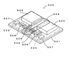
- the first and second filter units 503 and 505 having different signal passbands are arranged close to each other so that the characteristics of the filter units 503 and 505 are not deteriorated.
- the duplexer 500 with improved performance is mounted on a mounting substrate included in the circuit module, thereby reducing the size and performance of the circuit module.
- a conventional duplexer 500 shown in FIG. 9 has a SAW (surface acoustic wave) on a mounting surface of a base substrate 501 made of a resin, ceramic, or polymer material such as a printed circuit board, LTCC, alumina substrate, glass substrate, or composite material substrate.
- SAW surface acoustic wave
- first filter unit 503 including the filter element 502 and a second filter unit 505 including the SAW filter element 504.
- the first and second filter units 503 and 505 each include a SAW filter element.
- peripheral circuit elements that complement the electrical characteristics of 502 and 504 passive elements such as a chip inductor 506 and a chip capacitor 507 are provided.
- a boundary part 508 between the first filter unit 503 and the second filter unit 505 is used.
- the adjacent chip inductors 506 are arranged on the base substrate 501 so that the directions of the magnetic fluxes are substantially orthogonal to each other. With this configuration, even when the filter units 503 and 505 are arranged close to each other, signal interference between the first and second filter units 503 and 505 is prevented, and the characteristic change of each filter unit 503 and 505 is prevented. Is reduced.
- the conventional duplexer 500 with reduced size and higher performance is mounted on the mounting substrate, and the first and second filter sections 503 and 505 of the duplexer 500 are respectively connected to the transmission filter and the transmission filter.
- a circuit module such as an antenna switch is formed.
- the duplexer 500 includes a transmission terminal for inputting a transmission signal from the mounting substrate side to the transmission filter, a reception terminal for outputting a reception signal from the reception filter to the mounting substrate side, and an output of the transmission filter.
- Antenna terminal (common terminal) connected to the input side and the input side of the reception filter, and a ground terminal, and the transmission board connected to the transmission terminal and the reception terminal of the duplexer 500 on the mounting board, respectively.
- An electrode and a receiving electrode are provided. Then, a transmission signal is output from the transmission electrode of the mounting substrate to the transmission filter included in the duplexer 500 via the transmission terminal, and the transmission signal input to the transmission filter is subjected to a predetermined filter process and is then separated. Output from 500 antenna terminals.
- a reception signal is input from the antenna terminal to the reception filter included in the duplexer 500, and the reception signal input to the reception filter is subjected to a predetermined filtering process and is received from the reception terminal of the duplexer 500 via the reception electrode. Output to the mounting board side.
- JP 2006-279604 A paragraphs 0022 to 0025, FIG. 1, etc.
- the transmission signal output from the transmission electrode of the mounting board to the transmission terminal of the duplexer 500 is the reception electrode input reception electrode side provided on the mounting board. May be interfered with a received signal that is input from the antenna terminal and output from the receiving terminal to the receiving electrode of the mounting substrate via the receiving filter. Therefore, in general, a transmission signal output from the transmission electrode of the mounting substrate to the transmission terminal of the duplexer 500 is input from the antenna terminal and passed from the reception terminal of the duplexer 500 via the reception filter.
- a ground electrode connected to the ground terminal of the duplexer 500 is provided on the mounting substrate between the transmitting electrode and the receiving electrode. ing.
- the transmission signal output to the transmission terminal of the waver 500 leaks to the ground electrode, and the transmission signal leaked to the ground electrode travels along the edge of the ground electrode to the reception electrode side and is demultiplexed via the reception filter. There is a risk of interference with the received signal output from the receiving terminal of the device 500 to the receiving electrode of the mounting substrate, which hinders the duplexer 500 from being downsized.
- the present invention has been made in view of the above-described problems, and an object thereof is to provide a technique capable of improving the isolation characteristics between a plurality of signal electrodes provided on a mounting substrate.
- a circuit module includes a plurality of signal electrodes, a ground electrode disposed so as to be insulated between the signal electrodes in a top view, and the ground electrode.
- a mounting substrate provided with a plurality of via conductors to be connected, and each via conductor is arranged so that an edge of the ground electrode overlaps at least a part of the end surface in a top view. It is characterized (claim 1).
- the edge of the ground electrode may have a bent portion (claim 2). This structure is practical because the ground electrode can be formed in an optimum shape between the plurality of signal electrodes provided on the mounting substrate.
- a part of the end face of the via conductor arranged at the bent part of the edge of the ground electrode is formed in the same shape as a part of the bent part.
- the bent portion of the edge of the ground electrode is preferably formed in an arc shape (claim 4).
- the diameter of the via conductor arranged at the bent portion of the edge of the ground electrode is larger than the diameter of the other via conductor arranged other than the bent portion.
- the ground electrode further includes a plurality of via conductors disposed at positions excluding the edge of the ground electrode, and the via conductors disposed so that the end surfaces thereof overlap the edge of the ground electrode. It is desirable that the diameter be larger than the diameter of each via conductor disposed at a position excluding the edge of the ground electrode.
- the mounting board is mounted with a duplexer having a transmission filter and a reception filter having different pass bands, and the duplexer includes a transmission terminal for input to the transmission filter, and the reception filter.
- a receiving terminal for output from the output terminal and a grounding terminal, and the mounting board is provided with a transmitting electrode connected to the transmitting terminal and a receiving electrode connected to the receiving terminal as the signal electrode.
- the ground electrode is provided between the transmission electrode and the reception electrode in a top view and connected to the ground terminal (Claim 7). This structure prevents the transmission signal that is output from the transmission electrode and leaked to the ground electrode from traveling around the edge of the ground electrode to the reception electrode side.
- the isolation characteristic between the transmission electrode and the reception electrode provided on the mounting substrate can be improved.
- the ground electrodes are provided in layers on the mounting substrate, and the ground electrodes of the respective layers are electrically connected (claim 8).
- a signal leaked from any one of the plurality of signal electrodes to the ground electrode is prevented from traveling around the edge of the ground electrode to other signal electrodes.
- the isolation characteristics between the plurality of signal electrodes provided can be improved.
- FIG. 5 is a diagram illustrating an example of isolation characteristics in the mounting substrate of FIG. 4. It is a top view which shows an example of the electrode shape of the mounting board
- FIG. 1 is a diagram showing a first embodiment of a circuit module according to the present invention.
- FIG. 2 is a block diagram showing the internal configuration of the circuit module of FIG.
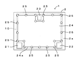
- FIG. 3 is a plan view showing an example of the electrode shape of the mounting substrate of the circuit module of FIG.
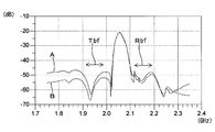
- FIG. 4 is a diagram showing an example of isolation characteristics in the mounting substrate of FIG.
- a circuit module 1 shown in FIG. 1 is mounted on a mother board MB included in a mobile communication terminal such as a mobile phone or a personal digital assistant.
- a mounting board 2 a duplexer 10
- the duplexer 10 and the component 3 are mounted on electrodes provided on the mounting surface 2 a of the mounting substrate 2, and the back surface of the mounting substrate 2 through the internal wiring pattern 5 provided on the mounting substrate 2. Are electrically connected to the plurality of mounting electrodes 6.
- various signal lines such as the antenna line ANT, the ground line GND, the transmission signal line Tx, the reception signal line Rx, and the power supply line provided in the mother board MB and the circuit module 1 are provided. Are connected, and transmission / reception signals are input / output between the mother board MB and the circuit module 1.
- the mounting substrate 2 is integrally formed as a ceramic laminate by laminating and firing a plurality of dielectric layers formed of ceramic green sheets.
- the internal wiring pattern 5 is formed by appropriately forming via conductors and electrode patterns.
- the ceramic green sheet forming each dielectric layer is a sheet in which a slurry in which a mixed powder such as alumina and glass is mixed with an organic binder and a solvent is formed into a sheet by a film forming apparatus. It is formed so as to be so-called low-temperature firing at the front and back temperatures. Then, via holes are formed in the ceramic green sheet cut into a predetermined shape by laser processing or the like, and the formed via holes are filled with a conductive paste containing Ag, Cu, etc. Via conductors are formed, various electrode patterns are formed by printing with a conductive paste, and each dielectric layer is formed.
- the internal wiring pattern 5 includes an electrode pattern and a via conductor for electrically connecting the duplexer 10 and various components 3 mounted on the circuit module 1 and the mounting electrode 6 to each other. It is formed by being provided in the layer. At this time, a circuit element such as a capacitor or a coil is formed by the electrode pattern and via conductor forming the internal wiring pattern 5, or a filter circuit or a matching circuit is formed by the circuit element such as a capacitor or coil by the electrode pattern and via conductor. May be.
- the duplexer 10 is used to separate a transmission signal and a reception signal having different frequencies. As illustrated in FIG. 2, the duplexer 10 includes a transmission filter 11 and a high-frequency signal having different passbands. A reception filter 12 is provided. The transmission filter 11 and the reception filter 12 are each formed by a SAW (surface acoustic wave) filter element.
- SAW surface acoustic wave
- the duplexer 10 is connected to the transmission terminal 13 for input to the transmission filter 11, the reception terminal 14 for output from the reception filter 12, the output side of the transmission filter 11, and the input side of the reception filter 12.
- the common terminal 15 (antenna terminal) and the ground terminal 16 are connected to the transmission electrode 21, the reception electrode 22, the common electrode 23, and the ground electrode 24 provided on the mounting substrate 2, respectively.
- the transmission filter 11 and the reception filter 12 included in the duplexer 10 are formed by SAW filter elements.
- SAW filter elements a plurality of resonators, coils, and the like are connected for transmission.
- the filter 11 and the reception filter 12 may be formed, and any transmission filter 11 and reception filter 12 may be used as long as transmission signals and reception signals having different frequencies can be reliably demultiplexed.
- a general filter including the transmission filter 11 and the reception filter 12 may be adopted, and the configuration and operation thereof are well known, and therefore the configuration and operation of the duplexer 10 are detailed. Description is omitted.
- a transmission electrode 21 (signal electrode), a reception electrode 22 (signal electrode), and a common electrode 23 (signal signal) are formed on a predetermined inner layer surface of a plurality of dielectric layers forming the mounting substrate 2. Electrode) in a rectangular land shape. Further, the ground electrode 24 may be provided on the surface of the dielectric layer that is one layer below the dielectric layer provided with the mounting surface 2a, for example, and the ground electrode 24 includes the transmission electrode 21 and the reception electrode in a top view. 22 between the two.
- the electrode configuration in FIG. 3 is a partial extraction of the electrode arrangement in the vicinity immediately below the duplexer 10, and other wiring electrodes may be provided around this electrode.
- the ground electrode 24 has a shape in which rectangular cutouts are provided at three rectangular positions, and the transmission electrode 21, the reception electrode 22, and the common electrode 23 are grounded in a top view. They are arranged in three rectangular cutouts provided in the electrode 24, respectively.
- the mounting substrate 2 is provided with a plurality of via conductors 25 connected to the ground electrode 24, and each via conductor 25 is at least one end face on the side connected to the ground electrode 24 in a top view.
- the end edge 24a of the ground electrode 24 is disposed so as to overlap the part. That is, in this embodiment, at the position of the end edge 24a to which the via conductor 25 of the ground electrode 24 is connected, a land-like connection portion extending in a tongue shape from the end edge 24a is formed in a top view, Each via conductor 25 is connected to a land-like connection portion so that its end surface overlaps the end edge 24a.
- the ground electrode 24 is connected to the mounting electrode 6 connected to the ground line GND of the mother board MB by connecting a plurality of via conductors 25 of the internal wiring pattern 5.
- a plurality of via conductors 25 are connected at substantially equal intervals along the end edge 24a of the ground electrode 24 in a top view.
- the ground electrode 24 In order to prevent the transmission signal output from the transmission electrode 21 to the transmission terminal 13 of the duplexer 10 from flowing to the reception electrode 22 side via the ground electrode 24, the ground electrode 24 particularly in a top view.
- the end face of the via conductor 25 is preferably connected to an edge portion (end edge 24a) close to the transmission electrode 21 of the first electrode, and further, the receiving electrode 22 extends from the edge portion of the ground electrode 24 close to the transmission electrode 21 when viewed from above.
- the end faces of the plurality of via conductors 25 may be connected along the edge of the ground electrode 24 up to the edge close to.
- FIG. 3 only the transmitting electrode 21, the receiving electrode 22, the common electrode 23, the ground electrode 24, and the via conductor 25 connected to the ground electrode 24 are shown for ease of explanation. These electrodes and via conductors are not shown.
- the ground electrode 24 and the via conductor 25 provided inside the mounting substrate 2 are also shown by solid lines, and the dotted line in FIG. 3 indicates the mounting position on the mounting surface 2 a of the duplexer 10. Indicates.
- the ground terminal 16 of the duplexer 10 is connected to the ground electrode 24 via a mounting electrode provided on the mounting surface 2a and a via conductor connected to the electrode (not shown). 5, 7 and 8 used in the following description are also illustrated in the same manner as in FIG.
- a via hole is formed in a ceramic green sheet formed in a predetermined shape with a laser or the like, and a conductor paste is filled inside or via fill plating is performed to form a via conductor 25 for interlayer connection.
- Electrode patterns such as the reception electrode 22, the common electrode 23, and the ground electrode 24 are printed with a conductive paste, and a ceramic green sheet for forming each dielectric layer constituting the mounting substrate 2 is prepared.
- Each ceramic green sheet has a plurality of electrode patterns such as via conductors 25, transmission electrodes 21, reception electrodes 22, common electrodes 23, and ground electrodes 24 so that a large number of mounting substrates 2 can be formed at one time. Is provided.
- each dielectric layer is laminated to form a laminate.
- substrate 2 after baking is formed so that the area
- the assembly of the mounting substrate 2 is formed by firing the laminate at a low temperature while being pressurized.
- the duplexer 10 and the component 3 are mounted on the mounting surface 2a of the assembly of the mounting substrates 2, and the duplexer 10 and the component 3 are mounted.
- the mounting surface 2a of the assembly of mounting substrates 2 is filled with a mold resin, and this is heated and cured, whereby a mold layer (not shown) is provided on each mounting substrate 2 to form an assembly of circuit modules 1. Is done. Then, the assembly of the circuit modules 1 is divided individually to complete the circuit module 1.
- the transmission signal output from the transmission signal line Tx of the mother board MB to the transmission terminal 13 of the duplexer 10 via the mounting electrode 6 and the internal wiring pattern 5 is transmitted.
- the signal is input to the filter 11, subjected to a predetermined filtering process, output from the common terminal 15 to the mounting board 2 side, and the antenna line of the mother board MB via the internal wiring pattern 5 (matching circuit) and the mounting electrode 6.
- Output to ANT A reception signal input from the antenna line ANT of the mother board MB to the common terminal 15 of the duplexer 10 via the mounting electrode 6 and the internal wiring pattern 5 (matching circuit) is input to the reception filter 12.
- Predetermined filtering is performed, the signal is output from the receiving terminal 14 to the mounting substrate 2 side, and is output to the reception signal line Rx of the mother substrate MB via the internal wiring pattern 5 and the mounting electrode 6.
- the circuit module 1 including the mounting substrate 2 provided with the internal wiring pattern 5, the duplexer 10, the component 3, and the mold layer is not limited to the above-described manufacturing method, and may be formed by a known general manufacturing method.
- the mounting board 2 can be formed of a printed board, LTCC, alumina-based board, glass board, composite material board, single-layer board, multilayer board, etc. using resin, ceramic, polymer material, etc.
- the mounting substrate 2 may be formed by selecting an appropriate material as appropriate according to the purpose of use of the circuit module 1.
- the matching circuit is formed by the internal wiring pattern 5, but the matching circuit may be formed by a component 3 such as a chip coil mounted on the mounting surface 2 a of the mounting substrate 2.
- FIG. 4 is a diagram illustrating an example of isolation characteristics of the circuit module 1 including the mounting substrate 2 of FIG. 3, where the vertical axis indicates gain (dB), the horizontal axis indicates frequency (GHz), and the transmission electrode 21. 3 shows the magnitude of the signal observed at the receiving electrode 22 when a high frequency signal of each frequency is output to the transmission terminal 13 of the duplexer 10.
- Curve A in the figure shows the isolation characteristic according to the conventional configuration in which a plurality of via conductors 25 are arranged on the ground electrode 24 so that the end face does not overlap the end edge 24a of the ground electrode 24 when viewed from above. Show.
- a curve B in the figure shows the isolation characteristics by the configuration shown in FIG.
- the frequency band indicated by the arrow Tbf in FIG. 4 indicates the pass band of the high-frequency signal of the transmission filter 11
- the frequency band indicated by the arrow Rbf in FIG. 4 indicates the pass band of the high-frequency signal of the reception filter 12. Therefore, theoretically, among the high frequency signals output from the transmission electrode 21 to the transmission terminal 13 of the duplexer 10, the high frequency signals in the frequency bands indicated by the arrows Tbf and Rbf are directly transmitted to the reception electrode 22 via the ground electrode 24. If the signal does not wrap around, there is no possibility of being observed at the reception electrode 22, so that the transmission signal and the reception signal input / output to / from the duplexer 10 do not interfere with each other, so Is not observed (low gain).
- the gain of the high-frequency signal in the frequency band indicated by the arrows Tbf and Rbf observed at the receiving electrode 22 is shown by the curve B in FIG.
- the gain due to the configuration is lower. Therefore, the isolation characteristic of the circuit module 1 including the mounting substrate 2 shown in FIG. 3 is improved compared to the isolation characteristic in the conventional configuration.
- the duplexer 10 has the transmission terminal 13 for input to the transmission filter 11, the reception terminal 14 for output from the reception filter 12, and the ground terminal 16.
- the transmission electrode 21 connected to the transmission terminal 13 of the duplexer 10 and the reception electrode 22 connected to the reception terminal 14 of the duplexer 10 are signals.
- a ground electrode 24 provided as an electrode for use and connected to the ground terminal 16 of the duplexer 10 is disposed between the transmission electrode 21 and the reception electrode 22 in a top view.
- the plurality of via conductors 25 are arranged so that the end surface of the ground electrode 24 overlaps the end edge 24a of the ground electrode 24 when viewed from above.
- the transmission signal leaked to the ground electrode 24 is mainly the ground electrode 24. Therefore, the transmission signal leaked to the ground electrode 24 is likely to flow into the plurality of via conductors 25 arranged so that the end surface of the ground electrode 24 overlaps the end edge 24a of the ground electrode 24 in a top view. Become. Therefore, the transmission signal that is output from the transmission electrode 21 and leaked to the ground electrode 24 is prevented from wrapping around the edge 24a of the ground electrode 24 toward the reception electrode 22 side, so that the duplexer 10 is mounted.
- the isolation characteristic between the transmission electrode 21 and the reception electrode 22 provided on the mounting substrate 2 can be improved.
- the end edge 24a of the ground electrode 24 is formed in a bent portion, that is, the end edge 24a is formed with a bent shape, a plurality of signal electrodes (transmitting electrode 21, receiving signal) provided on the mounting substrate 2 are formed. Since the ground electrode 24 can be formed in an optimum shape between the electrode 22 and the common electrode 23), it is practical.
- the end surface of the ground electrode 24 on the end edge 24 a in the top view such as the central portion of the ground electrode 24 in the top view.
- a large number of via conductors 25 must be arranged at positions where the two do not overlap, resulting in an increase in manufacturing cost.
- the plurality of via conductors 25 are arranged so that the end surfaces thereof overlap the end edges 24a of the ground electrode 24 where the transmission signal leaked from the transmission electrode 21 to the ground electrode 24 concentrates when viewed from above.
- the number of via conductors 25 can be reduced because the transmission signal leaked to the ground electrode 24 can be efficiently flowed into the ground line GND of the mother board MB with fewer via conductors 25 than in the conventional configuration.
- the manufacturing cost can be reduced.
- FIG. 5 is a plan view showing an example of the electrode shape of the mounting board in the second embodiment of the circuit module of the present invention.
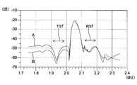
- FIG. 6 is a diagram illustrating an example of isolation characteristics in the mounting substrate of FIG. As shown in FIG. 5, this embodiment differs from the first embodiment described above in that the bent portion of the end edge 24a of the ground electrode 24 is formed in an arc shape, and the via conductor 25 arranged at the bent portion. A part of the end face is formed in the same shape as the part of the bent portion, that is, in an arc shape. Since other configurations are the same as those in the first embodiment, description of the configuration is omitted by giving the same reference numerals. Moreover, since FIG. 6 is the description similar to FIG. 4, the detailed description is abbreviate
- the gain of the high-frequency signal in the frequency band indicated by the arrows Tbf and Rbf observed at the receiving electrode 22 is a curve rather than the gain of the conventional configuration indicated by the curve A.
- the gain in the configuration of FIG. 5 indicated by B is lower. Therefore, the isolation characteristic of the circuit module 1 including the mounting substrate 2 shown in FIG. 5 is improved as compared with the isolation characteristic in the conventional configuration, and the same effect as that of the first embodiment described above can be obtained. .
- the transmission signal leaked from the transmission electrode 21 provided on the mounting substrate 2 to the ground electrode 24 concentrates on the bent portion of the edge 24a of the ground electrode 24, but is arranged in the bent portion.
- a part of the end surface of the via conductor 25 is formed in the same shape as a part of the bent portion, and the end surface of the via conductor 25 and the same shape of the bent portion of the end edge 24a are aligned.
- a transmission signal leaking from the transmission electrode 21 to the ground electrode 24 and concentrated on the bent portion of the ground electrode 24 can easily flow efficiently into the via conductor 25 arranged at the bent portion. Since the transmission signal leaked from 21 to the ground electrode 24 is more efficiently prevented from traveling around the receiving electrode 22 through the edge 24a of the ground electrode 24, the transmission electrode 21 provided on the mounting substrate 2 and The isolation characteristic between the receiving electrodes 22 can be further improved.
- the signal leaked from the transmission electrode 21 to the ground electrode 24 is concentrated on the bent portion of the edge 24 a of the ground electrode 24. Can be relaxed. Further, the transmission signal leaked from the transmission electrode 21 to the ground electrode 24 due to the bent portion of the edge 24a of the ground electrode 24 formed in an arc shape is transmitted to the reception electrode 22 transmitted through the edge 24a of the ground electrode 24. The wraparound can be suppressed.
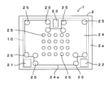
- FIG. 7 is a plan view showing an example of the electrode shape of the mounting board in the third embodiment of the circuit module of the present invention.
- this embodiment is different from the first embodiment described above in that the ground electrode 24 further includes a position excluding the edge 24a of the ground electrode 24, that is, a substantially central portion in a top view.
- a plurality of via conductors 25 are arranged, and the diameter of each via conductor 25 arranged so that the end surface thereof overlaps the end edge 24 a of the ground electrode 24 is arranged at a position excluding the end edge 24 a of the ground electrode 24.
- each via conductor 25 is larger than that of the via conductor 25.
- the ground electrode 24 has a shape in which rectangular cutouts are provided at three rectangular locations, and the bent portion of the edge 24a is formed at a right angle. Since other configurations are the same as those in the first embodiment, description of the configuration is omitted by giving the same reference numerals.
- the ground electrode 24 is further provided with a plurality of via conductors 25 at a substantially central portion in a top view excluding the end edge 24 a of the ground electrode 24.
- the diameter of each via conductor 25 arranged so that its end face overlaps with 24 a is formed larger than the diameter of each via conductor 25 arranged at a position excluding the end edge 24 a of the ground electrode 24.
- each via conductor 25 arranged at the bent portion of the end edge 24a of the ground electrode 24 is arranged at a portion other than the bent portion, including the via conductor 25 arranged with its end face superimposed on the end edge 24a.
- the transmission signal leaked from the transmission electrode 21 provided on the mounting substrate 2 to the ground electrode 24 is concentrated on the bent portion of the edge 24a of the ground electrode 24, but the diameter of the via conductor 25 arranged in the bent portion. Is formed larger than the diameter of the other via conductors 25 other than the bent portion, the contact area between the ground electrode 24 and the end face of the via conductor 25 in the bent portion is increased, and the via conductor is also formed. Since the diameter of the conductor 25 is large, the electrical resistance of the via conductor 25 is reduced, and the leaked transmission signal concentrated on the bent portion easily flows into the via conductor 25.
- the transmission signal leaked from the transmission electrode 21 to the ground electrode 24 and concentrated on the bent portion efficiently flows into the via conductor 25 disposed on the bent portion, so that the transmission signal leaked to the ground electrode 24 is Since the wraparound to the receiving electrode 22 transmitted through the edge 24a of the ground electrode 24 is further efficiently prevented, a plurality of signal electrodes (transmitting electrode 21, receiving electrode 22, common electrode) provided on the mounting substrate 2 are prevented. 23) can be further improved in isolation characteristics.
- FIG. 8 is a plan view showing an example of the electrode shape of the mounting board in the fourth embodiment of the circuit module of the present invention.
- this embodiment is different from the third embodiment described above in that the via conductor 25 arranged in the bent portion of the ground electrode 24 is formed in a prismatic shape, and is arranged in the bent portion. A part of the end face of the via conductor 25 is formed in the same shape as a part of the bent portion. Since other configurations are the same as those in the third embodiment described above, description of the configurations is omitted by giving the same reference numerals.
- the end face of the ground electrode 24 and the via conductor 25 in this bent part will be arrange
- the ground electrode 24 may be provided in layers on the mounting substrate 2, and the ground electrode 24 of each layer may be electrically connected by a plurality of via conductors 25.
- substrate 2 over several layers is connected by the via conductor 25, the transmission signal output from the transmission electrode 21 and leaked to the ground electrode 24 is In the top view, since it becomes easier to flow into the plurality of via conductors 25 arranged so that the end surface of the ground electrode 24 overlaps the end edge 24a, the transmission signal leaked to the ground electrode 24 is It is possible to more efficiently prevent the antenna 24 from going to the receiving electrode 22 side through the edge 24a of the 24, and the isolation characteristic between the transmitting electrode 21 and the receiving electrode 22 provided on the mounting substrate 2 on which the duplexer 10 is mounted. Can be further improved.
- the ground electrodes 24 provided on the mounting substrate 2 over a plurality of layers may have the same shape, but at least the portion adjacent to the transmission electrode 21 in the top view should have the same shape.
- the transmission signal output from the transmission electrode 21 and leaked to the ground electrode 24 can be efficiently guided to the plurality of via conductors 25 arranged so that the end surface thereof overlaps the end edge 24 a of the ground electrode 24. .
- the plurality of via conductors 25 be disposed along the edge 24a close to the transmission electrode 21 of the ground electrode 24 in a top view, and the ground electrode 24 is mounted on the mounting surface 2a of the mounting substrate 2.
- the ground electrode 24 may be provided in a lower layer of the mounting substrate 2.
- the shape of the transmission electrode 21, the reception electrode 22, and the common electrode 23a provided on the mounting surface 2a of the mounting substrate 2 is not limited to a rectangular shape, and the duplexer 10 such as a circular shape can be mounted. As long as it is possible, it may have any shape, and the ground electrode 24 is not necessarily formed so as to surround the rectangular transmission electrode 21, reception electrode 22, and common electrode 23 in a top view. In addition, the shape of the ground electrode 24 in a top view may be any shape as long as it is disposed between the transmission electrode 21, the reception electrode 22, and the common electrode 23, that is, between a plurality of signal electrodes.
- the signal electrodes are not limited to the electrodes 21 to 23 for connection to the terminals 13 to 15 of the duplexer 10 described above.
- the outer peripheral portion of the via conductor 25 may be disposed so as to protrude from the end edge 24 a of the ground electrode 24 toward the end edge side of the mounting substrate 2.
- the via conductor close to the edge of the mounting substrate 2
- the current leaking to the ground electrode can be concentrated on the edge of the ground electrode, so that the isolation characteristics between the transmission electrode 21 and the reception electrode 22 are further improved. Can be improved.
- the size of the ground electrode can be increased only by the portion where the outer peripheral portion of the via conductor 25 protrudes outward from the end edge 24a of the ground electrode 24, the size of the ground electrode can be increased.
- the present invention is provided with a plurality of signal electrodes such as various components and circuit patterns, a ground electrode disposed between the signal electrodes in a top view, and a plurality of via conductors connected to the ground electrode.
- the present invention can be widely applied to a circuit module including a mounting substrate.
Landscapes
- Engineering & Computer Science (AREA)
- Computer Networks & Wireless Communication (AREA)
- Signal Processing (AREA)
- Transceivers (AREA)
- Structure Of Printed Boards (AREA)
Abstract
Description
本発明の分波器(デュプレクサ)を備える回路モジュールの第1実施形態について、図1~図4を参照して説明する。図1は本発明の回路モジュールの第1実施形態を示す図である。図2は図1の回路モジュールの内部構成を示すブロック図である。図3は図1の回路モジュールの実装用基板の電極形状の一例を示す平面図である。図4は図3の実装用基板におけるアイソレーション特性の一例を示す図である。
図1に示す回路モジュール1は、携帯電話や携帯情報端末などの携帯通信端末が備えるマザー基板MBに搭載されるものであり、この実施形態では、実装用基板2と、分波器10と、スイッチICやフィルタ、抵抗、コンデンサ、コイルなどの各種の部品3とを備え、高周波アンテナスイッチモジュールとして形成されている。また、分波器10および部品3は、実装用基板2の実装面2aに設けられた電極に実装されて、実装用基板2に設けられた内部配線パターン5を介して実装用基板2の裏面に形成された複数の実装用電極6に電気的に接続される。そして、回路モジュール1がマザー基板MBに実装されることにより、マザー基板MBが備えるアンテナラインANTやグランドラインGND、送信信号ラインTx、受信信号ラインRxなどの各種信号ラインおよび電源ラインと回路モジュール1とが接続されて、マザー基板MBと回路モジュール1との間で送受信信号の入出力が行われる。
分波器10は、周波数の異なる送信信号と受信信号とを分離するために用いられるものであり、図2に示すように、分波器10は、高周波信号の通過帯域が異なる送信フィルタ11および受信フィルタ12を備えている。送信フィルタ11および受信フィルタ12は、それぞれSAW(表面弾性波)フィルタ素子により形成されている。
次に、図3を参照して、実装用基板2に設けられた送信電極21、受信電極22、共通電極23および接地電極24の電極形状の一例について説明する。
次に、図1の回路モジュール1の製造方法の一例についてその概略を説明する。
次に、図4を参照して、図3に示す接地電極24が実装用基板2に設けられた回路モジュール1の、送信電極21と受信電極22との間のアイソレーション特性について説明する。
次に、図5および図5を参照して本発明の第2実施形態について説明する。図5は本発明の回路モジュールの第2実施形態における実装用基板の電極形状の一例を示す平面図である。図6は図5の実装用基板におけるアイソレーション特性の一例を示す図である。この実施形態が上記した第1実施形態と異なる点は、図5に示すように、接地電極24の端縁24aの屈曲部分が円弧状に形成されて、該屈曲部分に配置されるビア導体25の端面の一部形状が、該屈曲部分の一部と同形状、すなわち円弧状に形成されている点である。その他の構成は上記した第1実施形態と同様の構成であるため、同一符号を付すことによりその構成の説明は省略する。また、図6は、図4と同様の記載であるため、同一符号を付すことによりその詳細な説明は省略する。
次に、図7を参照して本発明の第3実施形態について説明する。図7は本発明の回路モジュールの第3実施形態における実装用基板の電極形状の一例を示す平面図である。この実施形態が上記した第1実施形態と異なる点は、図7に示すように、接地電極24には、当該接地電極24の端縁24aを除く位置、すなわち、上面視における略中央部分にさらに複数のビア導体25が配置されており、当該接地電極24の端縁24aにその端面が重なるように配置される各ビア導体25の径は、当該接地電極24の端縁24aを除く位置に配置される各ビア導体25の径よりも大きく形成されている点である。また、接地電極24は、矩形の3箇所にそれぞれ矩形状の切欠きが設けられた形状を成し、端縁24aの屈曲部分は直角に形成されている。その他の構成は上記した第1実施形態と同様の構成であるため、同一符号を付すことによりその構成の説明は省略する。
次に、図8を参照して本発明の第4実施形態について説明する。図8は本発明の回路モジュールの第4実施形態における実装用基板の電極形状の一例を示す平面図である。この実施形態が上記した第3実施形態と異なる点は、図8に示すように、接地電極24の屈曲部分に配置されるビア導体25が角柱状に形成されることで、該屈曲部分に配置されるビア導体25の端面の一部形状が、該屈曲部分の一部と同形状に形成されている点である。その他の構成は上記した第3実施形態と同様の構成であるため、同一符号を付すことによりその構成の説明は省略する。
2 実装用基板
10 分波器
11 送信フィルタ
12 受信フィルタ
13 送信端子
14 受信端子
16 接地端子
21 送信電極(信号用電極)
22 受信電極(信号用電極)
23 共通電極(信号用電極)
24 接地電極
24a 端縁
25 ビア導体
Claims (8)
- 複数の信号用電極と、上面視において前記各信号用電極の間に絶縁されるように配置された接地電極と、前記接地電極に接続される複数のビア導体とが設けられた実装用基板を備え、
前記各ビア導体は、上面視において、少なくともその端面の一部に前記接地電極の端縁が重なるように配置されることを特徴とする回路モジュール。 - 前記接地電極の端縁が屈曲部分を有していることを特徴とする請求項1に記載の回路モジュール。
- 前記接地電極の端縁の屈曲部分に配置される前記ビア導体の端面の一部形状が、該屈曲部分の一部と同形状に形成されることを特徴とする請求項2に記載の回路モジュール。
- 前記接地電極の端縁の屈曲部分が円弧状に形成されることを特徴とする請求項2または3に記載の回路モジュール。
- 前記接地電極の端縁の屈曲部分に配置される前記ビア導体の径は、該屈曲部分以外に配置される他の前記ビア導体の径よりも大きく形成されることを特徴とする請求項2ないし4のいずれかに記載の回路モジュール。
- 前記接地電極には、当該接地電極の端縁を除く位置にさらに複数のビア導体が配置されており、
当該接地電極の端縁にその端面が重なるように配置される前記各ビア導体の径は、当該接地電極の端縁を除く位置に配置される前記各ビア導体の径よりも大きく形成されることを特徴とする請求項1ないし4のいずれかに記載の回路モジュール。 - 前記実装用基板には、通過帯域が異なる送信フィルタおよび受信フィルタを有する分波器が実装されており、
前記分波器は、前記送信フィルタへの入力用の送信端子と、前記受信フィルタからの出力用の受信端子と、接地端子とを有し、
前記実装用基板には、前記送信端子と接続される送信電極および前記受信端子と接続される受信電極が前記信号用電極として設けられ、上面視において前記送信電極および前記受信電極の間に配置されて前記接地端子と接続される前記接地電極が設けられていることを特徴とする請求項1ないし6のいずれかに記載の回路モジュール。 - 前記接地電極は、前記実装用基板に層状に設けられており、前記各層の接地電極が電気的に接続されることを特徴とする請求項1ないし7のいずれかに記載の回路モジュール。
Priority Applications (3)
| Application Number | Priority Date | Filing Date | Title |
|---|---|---|---|
| CN201280030610.5A CN103620958B (zh) | 2011-06-21 | 2012-06-13 | 电路模块 |
| DE112012002565.2T DE112012002565B4 (de) | 2011-06-21 | 2012-06-13 | Schaltungsmodul |
| US14/100,103 US10326489B2 (en) | 2011-06-21 | 2013-12-09 | Circuit module |
Applications Claiming Priority (2)
| Application Number | Priority Date | Filing Date | Title |
|---|---|---|---|
| JP2011136992 | 2011-06-21 | ||
| JP2011-136992 | 2011-06-21 |
Related Child Applications (1)
| Application Number | Title | Priority Date | Filing Date |
|---|---|---|---|
| US14/100,103 Continuation US10326489B2 (en) | 2011-06-21 | 2013-12-09 | Circuit module |
Publications (1)
| Publication Number | Publication Date |
|---|---|
| WO2012176401A1 true WO2012176401A1 (ja) | 2012-12-27 |
Family
ID=47422260
Family Applications (1)
| Application Number | Title | Priority Date | Filing Date |
|---|---|---|---|
| PCT/JP2012/003842 Ceased WO2012176401A1 (ja) | 2011-06-21 | 2012-06-13 | 回路モジュール |
Country Status (5)
| Country | Link |
|---|---|
| US (1) | US10326489B2 (ja) |
| JP (1) | JP5618003B2 (ja) |
| CN (1) | CN103620958B (ja) |
| DE (1) | DE112012002565B4 (ja) |
| WO (1) | WO2012176401A1 (ja) |
Cited By (2)
| Publication number | Priority date | Publication date | Assignee | Title |
|---|---|---|---|---|
| WO2017077853A1 (ja) * | 2015-11-04 | 2017-05-11 | 株式会社村田製作所 | 回路基板 |
| KR20170132308A (ko) * | 2015-06-03 | 2017-12-01 | 가부시키가이샤 무라타 세이사쿠쇼 | 고주파 프론트 엔드 회로 |
Families Citing this family (2)
| Publication number | Priority date | Publication date | Assignee | Title |
|---|---|---|---|---|
| JP6443263B2 (ja) | 2015-08-10 | 2018-12-26 | 株式会社村田製作所 | 高周波モジュール |
| TWI778766B (zh) | 2021-08-27 | 2022-09-21 | 立積電子股份有限公司 | 濾波器積體電路 |
Citations (3)
| Publication number | Priority date | Publication date | Assignee | Title |
|---|---|---|---|---|
| WO2005107068A1 (ja) * | 2004-04-30 | 2005-11-10 | Sanyo Electric Co., Ltd. | フィルターデバイス用基体及びフィルターデバイス |
| JP2009296508A (ja) * | 2008-06-09 | 2009-12-17 | Fujitsu Media Device Kk | 分波器 |
| JP2010220231A (ja) * | 2000-11-01 | 2010-09-30 | Hitachi Metals Ltd | 高周波スイッチモジュール |
Family Cites Families (10)
| Publication number | Priority date | Publication date | Assignee | Title |
|---|---|---|---|---|
| JPH11251587A (ja) | 1998-03-03 | 1999-09-17 | Fujitsu Ltd | 半導体装置及びその製造方法 |
| JP2002094204A (ja) | 2000-09-19 | 2002-03-29 | Matsushita Electric Ind Co Ltd | 高周波モジュールとその製造方法 |
| JP2003198419A (ja) | 2001-10-02 | 2003-07-11 | Matsushita Electric Ind Co Ltd | 高周波スイッチ及び無線通信機器 |
| JP2003309403A (ja) | 2002-04-17 | 2003-10-31 | Hitachi Ltd | 高周波回路基板 |
| JP2006279604A (ja) | 2005-03-29 | 2006-10-12 | Tdk Corp | 弾性表面波装置 |
| DE102005032058B4 (de) | 2005-07-08 | 2016-12-29 | Epcos Ag | HF-Filter mit verbesserter Gegenbandunterdrückung |
| US7674719B2 (en) | 2005-08-01 | 2010-03-09 | Panasonic Corporation | Via hole machining for microwave monolithic integrated circuits |
| JP4304677B2 (ja) | 2006-11-27 | 2009-07-29 | 日立金属株式会社 | 複合積層モジュール及びこれを用いた通信機 |
| US8367941B2 (en) * | 2008-02-20 | 2013-02-05 | Taiyo Yuden Co., Ltd. | Filter, branching filter, communication module, and communication equipment |
| JP5177392B2 (ja) | 2008-03-17 | 2013-04-03 | Tdk株式会社 | 弾性表面波装置 |
-
2012
- 2012-06-13 DE DE112012002565.2T patent/DE112012002565B4/de not_active Expired - Fee Related
- 2012-06-13 JP JP2013521429A patent/JP5618003B2/ja not_active Expired - Fee Related
- 2012-06-13 WO PCT/JP2012/003842 patent/WO2012176401A1/ja not_active Ceased
- 2012-06-13 CN CN201280030610.5A patent/CN103620958B/zh not_active Expired - Fee Related
-
2013
- 2013-12-09 US US14/100,103 patent/US10326489B2/en active Active
Patent Citations (3)
| Publication number | Priority date | Publication date | Assignee | Title |
|---|---|---|---|---|
| JP2010220231A (ja) * | 2000-11-01 | 2010-09-30 | Hitachi Metals Ltd | 高周波スイッチモジュール |
| WO2005107068A1 (ja) * | 2004-04-30 | 2005-11-10 | Sanyo Electric Co., Ltd. | フィルターデバイス用基体及びフィルターデバイス |
| JP2009296508A (ja) * | 2008-06-09 | 2009-12-17 | Fujitsu Media Device Kk | 分波器 |
Cited By (5)
| Publication number | Priority date | Publication date | Assignee | Title |
|---|---|---|---|---|
| KR20170132308A (ko) * | 2015-06-03 | 2017-12-01 | 가부시키가이샤 무라타 세이사쿠쇼 | 고주파 프론트 엔드 회로 |
| KR101994799B1 (ko) * | 2015-06-03 | 2019-07-01 | 가부시키가이샤 무라타 세이사쿠쇼 | 고주파 프론트 엔드 회로 |
| US10498387B2 (en) | 2015-06-03 | 2019-12-03 | Murata Manufacturing Co., Ltd. | High-frequency front-end circuit |
| WO2017077853A1 (ja) * | 2015-11-04 | 2017-05-11 | 株式会社村田製作所 | 回路基板 |
| US10524353B2 (en) | 2015-11-04 | 2019-12-31 | Murata Manufacturing Co., Ltd. | Circuit board |
Also Published As
| Publication number | Publication date |
|---|---|
| JP5618003B2 (ja) | 2014-11-05 |
| CN103620958A (zh) | 2014-03-05 |
| CN103620958B (zh) | 2016-11-09 |
| DE112012002565B4 (de) | 2018-08-23 |
| US20140179364A1 (en) | 2014-06-26 |
| DE112012002565T5 (de) | 2014-02-27 |
| US10326489B2 (en) | 2019-06-18 |
| JPWO2012176401A1 (ja) | 2015-02-23 |
Similar Documents
| Publication | Publication Date | Title |
|---|---|---|
| JP6489182B2 (ja) | アンテナ一体型無線モジュール | |
| JP5807675B2 (ja) | 回路モジュール | |
| US9178491B2 (en) | Circuit module including duplexer | |
| US8838059B2 (en) | High-frequency circuit module | |
| US8963652B2 (en) | Duplexer and circuit module including the same | |
| JP5618003B2 (ja) | 回路モジュール | |
| WO2013011649A1 (ja) | 分波器 | |
| JP2014039236A (ja) | 高周波回路モジュール | |
| JP5420102B1 (ja) | 高周波回路モジュール | |
| JP5420101B1 (ja) | 高周波回路モジュール | |
| JP2014039268A (ja) | 高周波回路モジュール | |
| JP5420103B1 (ja) | 高周波回路モジュール |
Legal Events
| Date | Code | Title | Description |
|---|---|---|---|
| 121 | Ep: the epo has been informed by wipo that ep was designated in this application |
Ref document number: 12801976 Country of ref document: EP Kind code of ref document: A1 |
|
| ENP | Entry into the national phase |
Ref document number: 2013521429 Country of ref document: JP Kind code of ref document: A |
|
| WWE | Wipo information: entry into national phase |
Ref document number: 112012002565 Country of ref document: DE Ref document number: 1120120025652 Country of ref document: DE |
|
| 122 | Ep: pct application non-entry in european phase |
Ref document number: 12801976 Country of ref document: EP Kind code of ref document: A1 |