WO2012176366A1 - 距離計測方法および装置 - Google Patents
距離計測方法および装置 Download PDFInfo
- Publication number
- WO2012176366A1 WO2012176366A1 PCT/JP2012/002767 JP2012002767W WO2012176366A1 WO 2012176366 A1 WO2012176366 A1 WO 2012176366A1 JP 2012002767 W JP2012002767 W JP 2012002767W WO 2012176366 A1 WO2012176366 A1 WO 2012176366A1
- Authority
- WO
- WIPO (PCT)
- Prior art keywords
- frequency
- light
- optical
- distance measuring
- modulator
- Prior art date
Links
Images


Classifications
-
- G—PHYSICS
- G01—MEASURING; TESTING
- G01S—RADIO DIRECTION-FINDING; RADIO NAVIGATION; DETERMINING DISTANCE OR VELOCITY BY USE OF RADIO WAVES; LOCATING OR PRESENCE-DETECTING BY USE OF THE REFLECTION OR RERADIATION OF RADIO WAVES; ANALOGOUS ARRANGEMENTS USING OTHER WAVES
- G01S17/00—Systems using the reflection or reradiation of electromagnetic waves other than radio waves, e.g. lidar systems
- G01S17/02—Systems using the reflection of electromagnetic waves other than radio waves
- G01S17/06—Systems determining position data of a target
- G01S17/08—Systems determining position data of a target for measuring distance only
- G01S17/32—Systems determining position data of a target for measuring distance only using transmission of continuous waves, whether amplitude-, frequency-, or phase-modulated, or unmodulated
- G01S17/36—Systems determining position data of a target for measuring distance only using transmission of continuous waves, whether amplitude-, frequency-, or phase-modulated, or unmodulated with phase comparison between the received signal and the contemporaneously transmitted signal
-
- G—PHYSICS
- G01—MEASURING; TESTING
- G01S—RADIO DIRECTION-FINDING; RADIO NAVIGATION; DETERMINING DISTANCE OR VELOCITY BY USE OF RADIO WAVES; LOCATING OR PRESENCE-DETECTING BY USE OF THE REFLECTION OR RERADIATION OF RADIO WAVES; ANALOGOUS ARRANGEMENTS USING OTHER WAVES
- G01S7/00—Details of systems according to groups G01S13/00, G01S15/00, G01S17/00
- G01S7/48—Details of systems according to groups G01S13/00, G01S15/00, G01S17/00 of systems according to group G01S17/00
- G01S7/481—Constructional features, e.g. arrangements of optical elements
- G01S7/4818—Constructional features, e.g. arrangements of optical elements using optical fibres
Definitions
- the present invention relates to a distance measuring method and a distance measuring apparatus for measuring the shape of medium / large products (turbine, railcar, escalator, automobile, airplane, etc.) with high accuracy.
- the distance measuring device of Patent Document 1 uses a femtosecond mode-locked pulse laser device.
- the distance measuring device of Patent Document 2 applies frequency modulation to a continuous light by a modulating light modulator, irradiates an object, and demodulates and detects reflected light by a demodulating light modulator.
- JP 2006-184181 A Japanese Patent No. 3089376
- the distance measuring device of Patent Document 1 needs to use about several millimeters as a measure with the shortest period in order to measure distance with an accuracy of several tens of ⁇ m (when the phase measurement accuracy is about 2 ⁇ / 100), and the frequency It is necessary to handle about several tens of GHz. High frequency products in the tens of GHz band are expensive and equipment costs are high.
- the present invention performs optical beat-down using a light modulator for light from a light source that oscillates a plurality of frequencies, and detects the phase at a low frequency, thereby increasing the measurement accuracy without increasing the apparatus cost.
- the purpose is to increase.
- the present invention modulates the frequency of a light source that oscillates a plurality of lights having different frequencies, the light from the light source, and the light from the light source that is reflected after being irradiated on a measurement target.
- a light modulator an oscillator for inputting an electric signal to the light modulator, a detector for detecting the light signal modulated by the light modulator, and a distance from the phase of the light signal detected by the detector.
- a distance measuring device comprising a distance calculating circuit for calculating.
- the present invention oscillates light of a plurality of different frequencies from a light source and irradiates the measurement target, modulates the frequency of the light from the light source and the light reflected from the measurement target, and is modulated.
- a distance measurement method is provided, in which the detected light is detected by a detector, and the distance is calculated from the phase of the optical signal between the detected light reflected from the measurement object and the oscillated light.
- light from a light source that oscillates a plurality of frequencies is optically beat-down using an optical modulator, and phase detection is performed at a low frequency, thereby improving measurement accuracy without increasing the apparatus cost. it can.
- FIG. 3 is an apparatus configuration diagram in which an optical comb in the first embodiment is used as a light source and optical beat down is performed by an optical waveguide intensity modulator.
- 3 is a graph showing a spectrum of frequencies detected in the first embodiment.
- FIG. 7 is a device configuration diagram in which optical beat down is performed by an optical waveguide intensity modulator using two LDs in the second embodiment as light sources. It is a graph which shows the spectrum of the frequency detected in the 2nd example. It is a figure explaining the structure of the electroabsorption type modulator in a 3rd Example. It is a graph which shows the spectrum of the frequency after passing an electro-absorption type intensity modulator in the 3rd example.
- FIG. 10 is an apparatus configuration diagram for optical beat-down by an electroabsorption modulator using two LDs as light sources in the fourth embodiment. It is a graph which shows the spectrum of the frequency detected in the 4th example. It is an apparatus block diagram which uses the optical comb in a 5th Example as a light source, optical beats down with an optical waveguide intensity modulator, and extracts the beat component from which a frequency differs with multiple types of band pass filters. It is a graph which shows the spectrum of the frequency detected in a 5th Example.
- FIG. 10 is a device configuration diagram in which a plurality of LDs having different frequencies in the sixth embodiment are used as light sources, optical beat down is performed by an optical waveguide intensity modulator, and beat components having different frequencies are extracted by a plurality of types of bandpass filters. It is a graph which shows the spectrum of the frequency detected in a 6th Example.
- FIG. 10 is an apparatus configuration diagram combining a time-of-flight method in a seventh embodiment and fifth and sixth embodiments.
- FIG. 10 is a configuration diagram of a three-dimensional distance measuring device equipped with the distance measuring optical system mechanism described in the first to seventh embodiments. It is a device block diagram for keeping the difference frequency of two LDs in the ninth embodiment constant.
- Fig. 11 shows the characteristics of the femtosecond mode-locked pulse laser.
- the femtosecond mode-locked pulse laser is an ultrashort pulse train with a very stable pulse interval in the time domain.
- a large number of stable optical frequency mode trains are arranged at constant frequency intervals. Since this optical frequency mode sequence shows a discrete spectral structure like a comb tooth, it is called an optical (frequency) comb.
- the frequency interval between the comb teeth is called a repetition frequency (frep).
- frep is the reciprocal of the pulse interval of the ultrashort pulse train.
- Fig. 12 (a) shows a high-precision distance measuring device using an optical comb.
- An optical comb is used as the light source 1201.
- a part of the beam is divided by a beam splitter 1202, detected by a light receiver 1203, and used as a reference signal.
- the main part of the beam is irradiated onto the measuring object 1205, the reflected light returns to the main body again, and is detected by the light receiver 1204 to become a probe signal.
- a frequency component used for distance measurement is selected from a number of frequency components included in the probe signal by a band pass filter, and a phase difference from the reference signal is measured by a phase meter 119 to obtain distance information 120.
- Fig. 12 (b) shows the principle of measuring long distances with high accuracy.
- distance measurement is performed with low accuracy using a ruler 1 with a long period that makes the measurement range within one period.
- the distance measurement accuracy is improved by using a ruler 2 having a period within which the accuracy obtained with the ruler 1 is within one cycle.
- the distance is measured with high accuracy using a ruler 3 with a period that will ultimately achieve the target accuracy.
- FIG. 13 shows a configuration diagram of a distance measuring device using an optical comb.
- a 40 GHz detector 1301, a mixer 1302, an oscillator 103, and a power divider 106 are required to detect a 40 GHz beat signal.
- the frequency to be handled is 40 GHz (measurement length 3.75 mm).
- the distance measuring device shown in FIG. 13 needs to use several millimeters as a rule with the shortest period in order to measure distances with an accuracy of several tens of ⁇ m (when the phase measurement accuracy is about 2 ⁇ / 100), and the frequency It is necessary to handle about several tens of GHz.
- the high frequency compatible products in the tens of GHz band are expensive and there is a problem that the equipment cost is high.
- FIG. 14 shows a Mach-Zehnder type optical waveguide intensity modulator as an example of the optical modulator.
- the light incident from the input port is branched into two, the light incident on one waveguide passes through as it is, and the light applied to the other waveguide has a voltage applied to the element.
- the phase modulation is applied by giving a change in the refractive index in the optical path by adding.
- the light intensity may be increased or decreased depending on the phase difference, so that the light intensity can be modulated.
- FIG. 14B shows an optical spectrum after passing through the optical modulator.
- the modulation frequency of the voltage applied to the optical modulator is d ⁇
- the ⁇ first order component of ⁇ ⁇ d ⁇ the ⁇ second order component of ⁇ ⁇ 2d ⁇
- the ⁇ second order component of ⁇ ⁇ 3d ⁇ with respect to the frequency ⁇ of the incident continuous light.
- Sidebands occur for the third-order component and the continuous light frequency.
- the sideband intensity of each order can be adjusted by changing the bias voltage applied to the optical modulator.
- FIG. 15 shows a configuration diagram of a high-precision distance measuring device using an optical modulator.
- the light source 1501 emits continuous light and enters the modulation light modulator 1502.
- frequency modulation nf that is n times the frequency f ⁇ ⁇ can be applied to the incident light.
- the light that has passed through the optical modulator 1502 propagates into the space by the fiber collimator 107, passes through the polarization beam splitter 108 and the ⁇ / 4 plate 109, and is irradiated onto the object 110.
- the reflected light again passes through the ⁇ / 4 plate 109 and the polarization beam splitter 108 and enters the demodulating light modulator 1503.
- the modulation frequency of the voltage applied from the oscillator 1506 to the demodulating optical modulator is f + df
- n times frequency modulation nf + ndf can be given to the light
- the modulation frequency added by the modulating optical modulator The modulation frequency component of ndf, which is the difference frequency of, is emitted. Therefore, if a sufficiently small value (several MHz to several kHz) is selected as df, highly accurate distance measurement can be performed by the detector 1504 having a slow frequency response.
- a modulation signal of n times the modulation frequency of the applied voltage is used, distance measurement can be performed with an accuracy of n times the frequency of the oscillator.
- FIG. 11 In view of the problems of the distance measuring apparatus shown in FIGS. 11 and 15, a method for measuring distance with high accuracy using the optical comb and the optical waveguide intensity modulator in the developed embodiment 1 is shown in FIG. This will be described with reference to FIG.
- FIG. 1 (a) is an example of a configuration diagram of the distance measuring apparatus of the present embodiment.
- an optical comb that oscillates light having a plurality of discrete optical frequencies described in FIG. 11 is used as a light source.
- the optical comb irradiated from the optical comb generator 101 is irradiated into the space by the fiber collimator 107 and enters the polarization beam splitter 108.
- a part of the light is collected by the fiber collimator 111, enters the optical waveguide intensity modulator 112, and a main part passes through the ⁇ / 4 plate 109 and is irradiated onto the object 110.
- the reflected light from the object passes through the ⁇ / 4 plate 109 again, is reflected by the polarization beam splitter 108, is collected by the fiber collimator 115, and enters the optical waveguide intensity modulator 116.
- the oscillator 103 generates an electric signal having a frequency f, is branched into two by the power divider 106, and is input to the optical waveguide intensity modulators 112 and 116, respectively.
- the frequency modulated by the optical waveguide intensity modulators 112 and 116 is determined by the frequency of the electric signal generated by the oscillator 103.
- the light that has passed through the optical waveguide intensity modulator 112 is converted into an electrical signal by the light receiver 113, and only the frequency component used for distance measurement is extracted by the filter 114 and input as a reference signal for the phase meter 119.
- the light that has passed through the optical waveguide intensity modulator 116 is converted into an electrical signal by the light receiver 117, and only the frequency component used for distance measurement is extracted by the filter 118 and input as a measurement signal of the phase meter 119.
- the phase is calculated by the phase meter 119, and the distance is calculated by the distance calculation circuit 120.
- Fig. 1 (b) shows the principle of optical beat-down of an optical comb using an optical waveguide intensity modulator.
- the repetition frequency (frep) of the optical comb is 10.0001 MHz
- the frequency interval of a spectrum 10000 lines away from a certain spectrum is 100.001 GHz.
- this beat signal is used for distance measurement.
- frequency modulation is applied to the optical waveguide intensity modulators 112 and 116 from the oscillator 103 driven by the reference signal generator 104, and optical beat down is performed using the first-order sideband component.
- the frequency interval of a spectrum separated by 10,000 from a certain spectrum can be beaten down from 100.001 GHz to 1 MHz and detected by the light receiver 113.
- 50 GHz is given as the oscillation frequency of the oscillator 103, and the frequency interval of the spectrum separated by 10,000 from the same spectrum is beat-down from 100.001 GHz to 1 MHz. Can be detected.
- the optical waveguide intensity modulators 112 and 116 can perform optical modulation (optical beat down) at a frequency n times the frequency input from the oscillator 103. Further, if the optical beat down can be performed using higher-order sideband components, the oscillation frequency of the oscillator can be suppressed to a low frequency.
- the light emitted from the optical comb 101 passes through the optical waveguide intensity modulator 112 or the optical waveguide intensity modulator 116 only once, attenuation of high-order frequency components can be suppressed to a minimum. Can be detected with high accuracy.
- the frequency of the optical beat-down signal fluctuates, which may adversely affect the phase measurement accuracy.
- an oscillator 102 is provided to keep the frequency of the optical beat down signal constant.
- the phase of the optical beat-down signal and the oscillator 102 are compared (for example, phase comparison is possible by the mixer 121), and the error signal is input to the repetition frequency control mechanism of the optical comb 101, so that the frequency of the optical beat-down signal is constant.
- the repetition frequency of the optical comb is controlled so that At this time, the signal from the reference signal generator 104 is bifurcated by the power divider 105 and is used as an external reference signal for the oscillators 103 and 102, respectively, so that phase synchronization between the two oscillators is required. Thereby, the fluctuation of the frequency of the optical beat-down signal can be prevented, and the deterioration of the phase measurement accuracy can be suppressed.
- the optical comb 101 as a light source, optically beat down the high frequency beat component of the optical comb 101 using the optical waveguide intensity modulators 112 and 116, and detect the phase at a low frequency, Measurement accuracy can be increased without increasing the apparatus cost.
- Example 2 of the present invention will be described with reference to FIGS. 2 (a) and 2 (b).
- FIG. 2A is an example of a configuration diagram illustrating an apparatus using two LDs in the second embodiment.
- the description of the components having the same functions as those already described with reference to FIG. 1 is omitted.
- ⁇ Use LD201 and LD202 with slightly different oscillation frequencies as the light source The optical path is made the same by the coupler 203, is irradiated into the space by the fiber collimator 107, and enters the polarization beam splitter. A part of the light is collected by the fiber collimator 111, enters the optical waveguide intensity modulator 112, and a main part passes through the ⁇ / 4 plate 109 and is irradiated onto the object 110. The reflected light from the object passes through the ⁇ / 4 plate 109 again, is reflected by the polarization beam splitter 108, is collected by the fiber collimator 115, and enters the optical waveguide intensity modulator 116.
- Fig. 2 (b) shows the principle of optical beat-down of the beat component between two LDs using an optical waveguide intensity modulator.
- the frequency difference between LDs is 100.001 GHz.
- this beat signal is used for distance measurement.
- frequency modulation is applied from the oscillator 103 to the optical waveguide intensity modulator, and an optical beat down is performed using a primary sideband component.
- 100 / n GHz is given as the oscillation frequency of the oscillator 103, and it is possible to detect by beat down to 1 MHz. If the optical beat down can be performed using higher-order sideband components, the oscillation frequency of the oscillator can be suppressed to a low frequency.
- the frequency of the optical beat-down signal fluctuates, which may adversely affect the phase measurement accuracy.
- An oscillator 102 is provided to keep the frequency of the optical beat down signal constant.
- the phase of the optical beatdown signal and the oscillator 102 are compared (for example, the phase can be compared by the mixer 121), and the error signal is input to the oscillation frequency control mechanism of the LD201, thereby making the frequency of the optical beatdown signal constant. Control the oscillation frequency of LD201.
- the signal from the reference signal generator 104 is bifurcated by the power divider 105 and is used as an external reference signal for the oscillators 103 and 102, respectively, so that phase synchronization between the two oscillators is required.
- the fluctuation of the frequency of the optical beat-down signal can be prevented, and the deterioration of the phase measurement accuracy can be suppressed.
- optical beat-down of a high frequency beat component between the plurality of LDs using an optical waveguide intensity modulator, and detecting a phase at a low frequency Measurement accuracy can be increased without increasing costs.
- Example 3 of the present invention will be described with reference to FIGS. 3 (a), 3 (b), 4 (a), and 4 (b).
- FIG. 3A illustrates the principle of the electroabsorption intensity modulator.
- continuous light 301 is incident and irradiated onto the semiconductor element 306.
- the semiconductor element can change the absorptance with respect to the incident wavelength by an applied electric field. Therefore, the modulated light 302 can be obtained by modulating the applied electric field.
- FIG. 3B shows an optical spectrum after passing through the electroabsorption intensity modulator. If the modulation frequency of the voltage applied to the optical modulator is d ⁇ , a side band of ⁇ ⁇ d ⁇ is generated with respect to the frequency ⁇ of the incident continuous light.
- Fig. 4 (a) shows the device configuration using an electroabsorption intensity modulator.
- Electroabsorption modulators 401 and 402 are used for optical beat down.
- a fiber loop is provided for allowing light emitted from the electroabsorption modulator to enter the electroabsorption modulator 401 and 402 again for the purpose of optical beatdown at a frequency n times the frequency f applied from the oscillator 103.
- An optical amplifier 404 is introduced in the fiber loop in order to suppress light attenuation.
- the optical comb irradiated from the optical comb generator 101 is irradiated into the space by the fiber collimator 107 and enters the polarization beam splitter 108.
- a part of the light is collected by the fiber collimator 111 and enters the electroabsorption modulator 401, and a main part passes through the ⁇ / 4 plate 109 and is irradiated onto the object 110.
- the reflected light from the object passes through the ⁇ / 4 plate 109 again, is reflected by the polarization beam splitter 108, is collected by the fiber collimator 115, and enters the electroabsorption modulator 402.
- Fig. 4 (b) shows the principle of optical beat-down of an optical comb using an electroabsorption intensity modulator.
- the repetition frequency of the optical comb is 10.0001 MHz
- the spectrum exists at intervals of 10.0001 MHz on the frequency.
- the frequency interval of a spectrum 10000 lines away from a certain spectrum is 100.001 GHz.
- this beat signal is used for distance measurement.
- optical beat down is performed using a frequency component that has passed through the electroabsorption intensity modulators 401 and 402 once.
- 100 GHz is given as the oscillation frequency of the oscillator 103 and beats down to 1 MHz so that it can be detected by the light receiver 113.
- the oscillation frequency of the oscillator 103 is given as the oscillation frequency of the oscillator 103, and detection can be performed by beat down to 1 MHz.
- 100 / n GHz is given as the oscillation frequency of the oscillator 103, and it can be detected by beatdown to 1MHz. It becomes possible. If the optical beat down can be performed using the frequency component that has passed through the electroabsorption intensity modulator a plurality of times, the oscillation frequency of the oscillator can be suppressed to a low frequency.
- the phase comparison between the optical beat-down signal and the oscillator 102 is performed in the same manner as in the first embodiment (for example, phase comparison is possible by the mixer 121), and an error signal is input to the repetition frequency control mechanism of the optical comb 101.
- the repetition frequency of the optical comb is controlled so that the frequency of the optical beatdown signal is constant.
- an optical comb is used as a light source, and an optical absorption beat modulator is used to optically beat down the high frequency beat component of the optical comb, thereby detecting the phase at a low frequency, thereby increasing the device cost. Without increasing the measurement accuracy.
- an optical beat down due to a higher-order component of the modulation frequency can be achieved as in the case of using an optical waveguide intensity modulator.
- Example 4 of the present invention will be described with reference to FIGS. 5 (a) and 5 (b).
- FIG. 5A is an example of a device configuration diagram according to the fourth embodiment.
- the description of the components having the same functions as those already described with reference to FIG. 1 is omitted.
- ⁇ Use LD201 and LD202 with slightly different oscillation frequencies as the light source The optical path is made the same by the coupler 203, is irradiated into the space by the fiber collimator 107, and enters the polarization beam splitter. A part of the light is collected by the fiber collimator 111 and enters the electroabsorption-type intensity modulator 401, and a main part passes through the ⁇ / 4 plate 109 and is irradiated onto the object 110. The reflected light from the object passes through the ⁇ / 4 plate 109 again, is reflected by the polarization beam splitter 108, is collected by the fiber collimator 115, and enters the electroabsorption intensity modulator 402.
- Fig. 5 (b) shows the principle of optical beat-down of the beat component between two LDs using an electro-absorption intensity modulator.
- the frequency difference between LDs is 100.001 GHz.
- this beat signal is used for distance measurement.
- the optical beat-down using the component that has passed n times through the electro-absorption-type intensity modulator in the same way as in Example 3 giving 100 / n GHz as the oscillation frequency of the oscillator and detecting by beat-down to 1MHz It becomes possible to do. If the optical beat down can be performed using the frequency component that has passed through the electroabsorption intensity modulator a plurality of times, the oscillation frequency of the oscillator can be suppressed to a low frequency.
- the phase comparison between the optical beat-down signal and the oscillator 102 is performed as in the second embodiment (for example, phase comparison is possible by the mixer 121), and an error signal is input to the repetition frequency control mechanism of the optical comb 101.
- the difference frequency between the LD 201 and the LD 202 is controlled so that the frequency of the optical beat down signal is constant. Thereby, the fluctuation of the frequency of the optical beat-down signal can be prevented, and the deterioration of the phase measurement accuracy can be suppressed.
- an optical comb when used as a light source, many beat signals that are not used for distance measurement are generated, but in the case of LD, only beat signals that are used for distance measurement are generated, so that it is easy to extract beat signals by a filter.
- an electroabsorption modulator in the fiber loop an optical beat down due to a higher-order component of the modulation frequency can be achieved as in the case of using an optical waveguide intensity modulator.
- Embodiment 5 of the present invention will be described with reference to FIGS. 6 (a) and 6 (b).
- FIG. 6A is an example of a configuration diagram of the distance measuring apparatus of the present embodiment.
- the beat component detected by the light receiver 113 includes a beat component that is an integral multiple of the repetition frequency of the optical comb and a beat component that is optically beat-down by the optical waveguide intensity modulator. For example, as shown in FIG.
- the repetition frequency of the optical comb is 10.0001 MHz and the frequency at which the optical beat intensity is reduced by the optical waveguide intensity modulator is 100 GHz
- beats exist at intervals of 10.0001 MHz, and 10000
- the signal including these beat components is branched into three by the power divider 601 and the frequency components to be measured are extracted by the bandpass filters 603, 605, and 607, respectively.
- the pass center frequency of the band pass filter 603 is 1 MHz
- the pass center frequency of the band pass filter 605 is 10 MHz
- the pass center frequency of the band pass filter 603 is 1 GHz.
- the signal from the light receiver 117 is branched into three by the power divider 602, and the frequency components to be measured are extracted by the band pass filters 604, 606, and 608, respectively.
- the pass center frequencies of the bandpass filters 604, 606, and 608 are 1 MHz, 10 MHz, and 1 GHz, respectively.
- the phase meter 609 performs 1 MHz phase measurement
- the phase meter 610 performs 10 MHz phase measurement
- the phase meter 611 performs 1 GHz phase measurement.
- the distance calculation circuit 120 performs distance measurement from the three phase information. If each phase measurement accuracy is 2 ⁇ / 150 or less, the beat component with a frequency of 10 MHz has a distance measurement period of 15 m, and the distance measurement accuracy is 100 mm (1/150 of 15 m).
- the beat component with a frequency of 1 GHz has a distance measurement cycle of 150 mm, and the phase measurement accuracy is 1 mm (1/150 of 150 mm).
- the beat component with a frequency of 1 MHz (the component that optically beats 100.001 GHz) has a distance measurement period of 1.5 mm, and the phase measurement accuracy is 10 um (1/150 of 1.5 mm). Therefore, it is possible to measure a distance of 15m with an accuracy of 10um.
- the phase comparison between the optical beat-down signal and the oscillator 102 is performed in the same manner as in the first embodiment (for example, phase comparison is possible by the mixer 121), and an error signal is input to the repetition frequency control mechanism of the optical comb 101.
- the repetition frequency of the optical comb is controlled so that the frequency of the optical beatdown signal is constant.
- an optical comb is used as a light source, and an optical waveguide intensity modulator is used to optically beat down the high frequency beat component of the optical comb, thereby detecting the phase at a low frequency, thereby increasing the device cost. Without increasing the measurement accuracy. Further, by using a plurality of frequency components, it is possible to measure a long distance with high accuracy.
- Example 6 of the present invention will be described with reference to FIGS. 7 (a) and 7 (b).
- This embodiment is an example of an apparatus that measures phases of a plurality of frequencies and measures a long distance with high accuracy, and an example in which a plurality of LDs are used as a light source will be described.
- the description of the components having the same functions as those already described with reference to FIGS. 2 and 6 is omitted.
- two LDs are used and beats of a difference frequency are used for distance measurement.
- a plurality of beats can be generated by using a plurality of LDs. For example, a case where three types of beats are generated using four LDs will be described. As shown in FIG.
- the LD701, LD702, and LD201 are set so that the difference frequency is 10 MHz, 1 GHz, and 100.001 GHz with respect to the reference LD202.
- the beat frequency of the LD201 is optically beat down to 1 MHz by the optical waveguide intensity modulator.
- the beat frequencies detected by the light receiver 113 and the light receiver 117 are 1 MHz, 10 MHz, and 1 GHz.
- a distance of 15 m can be measured with an accuracy of 10 ⁇ m.
- the oscillator 102 is provided to keep the frequency of the signal obtained by optically beat-down the difference frequency between the LD 201 and the LD 202 constant.
- the optical beat-down signal is extracted by the power divider 612, the phase is compared with the oscillator 102 (for example, the phase can be compared by the mixer 121), and the optical beat is reduced by inputting the error signal to the LD oscillation frequency control mechanism.
- the LD oscillation frequency is controlled so that the signal frequency is constant.
- an oscillator 705 is provided to keep the difference frequency between LD202 and LD701 constant, the signal extracted by the power divider 613 is compared with the phase of the oscillator 705, and an error signal is input to the oscillation frequency control mechanism of the LD701.
- the difference frequency between LD202 and LD701 is kept constant.
- an oscillator 706 is provided to keep the difference frequency between LD202 and LD702 constant, the phase of the signal extracted by the power divider 614 and the oscillator 706 is compared, and an error signal is input to the oscillation frequency control mechanism of the LD701.
- the difference frequency between LD202 and LD702 is kept constant. Thereby, the fluctuation of the frequency of the optical beat-down signal can be prevented, and the deterioration of the phase measurement accuracy can be suppressed.
- beat signals that are not used for distance measurement are not generated, so extraction by filters is easy. Further, by using a plurality of frequency components, it is possible to measure a long distance with high accuracy.
- Example 7 of the present invention will be described with reference to FIG.
- the time-of-flight method is a method of irradiating pulsed light, hitting an object, and measuring the distance from the time when reflected light is detected by a light receiver to the object.
- the distance measurement range is not limited (depends on the detected light intensity), and the distance measurement accuracy is about several millimeters.
- Example 5 or 6 when measuring a long distance, it is necessary to prepare a number of rulers for distance measurement, and the configuration becomes large.
- FIG. 8 is an example of a configuration diagram of the distance measuring apparatus according to the present embodiment.
- the light source 801 for time-of-flight is made the same optical path as the optical comb or LD by the coupler 203.
- the light is irradiated into the space by the fiber collimator 107, enters the polarization beam splitter 108, passes through the ⁇ / 4 plate 109, and is irradiated onto the object 110.
- the reflected light from the object passes through the ⁇ / 4 plate 109 again, is reflected by the polarization beam splitter 108, and enters the time-of-flight receiver 802 by the beam splitter 803.
- the time of the pulse emitted from the time-of-flight light source 801 and the time of the pulse received by the time-of-flight light receiver 802 are input to the distance calculation circuit 804.
- d measurement distance
- c speed of light
- ⁇ t propagation time (reciprocation).
- the phase comparison between the optical beat-down signal and the oscillator 102 is performed in the same manner as in the first embodiment (for example, phase comparison is possible by the mixer 121), and an error signal is input to the repetition frequency control mechanism of the optical comb 101.
- the repetition frequency of the optical comb is controlled so that the frequency of the optical beatdown signal is constant.
- Example 8 of the present invention will be described with reference to FIG.
- FIG. 9 is an example of an apparatus configuration diagram of this embodiment.
- the light emitted from the distance measuring unit 903 is focused on the object 110 by the focus lens 902. This is because when the target object is a rough surface, the light returning to the distance measuring unit becomes weak due to scattering, so that a sufficient amount of light for detection can be obtained by focusing.
- the galvano scanner 901 enables three-dimensional beam scanning and enables three-dimensional shape measurement.
- a galvano scanner, a focus lens, and a power supply unit 904 for driving the distance measuring unit are provided, and a GUI unit 905 is provided for controlling the apparatus and displaying the distance measurement result.
- the galvano scanner enables three-dimensional shape measurement.
- Embodiment 9 of the present invention will be described with reference to FIGS. 10 (a), 10 (b), and 10 (c).
- FIG. 10 is an example of an apparatus configuration diagram of this embodiment.
- FIG. 10A shows an embodiment using an optical waveguide intensity modulator 1001.
- nf n-th sideband
- a frequency component having a side band is extracted by an optical filter and incident on the LD 202, whereby the incident side band component is amplified and output from the LD 202 (see FIG. 10C).
- FIG. 10B shows an embodiment using an electroabsorption modulator.
- Light emitted from the LD 201 enters the electroabsorption modulator.
- a component that has passed through the electroabsorption modulator n times by the fiber loop generates a modulation frequency nf (n-order sideband) that is n times the oscillation frequency f.
- a frequency component having a side band is extracted by an optical filter and incident on the LD 202, whereby the incident side band component is amplified and output from the LD 202.
- the frequency difference between the LDs is not controlled as an error signal, but the frequency difference between the LDs can be kept constant by the frequency stability of the oscillator, so that excellent stability can be obtained. Can do.
Landscapes
- Engineering & Computer Science (AREA)
- Physics & Mathematics (AREA)
- Computer Networks & Wireless Communication (AREA)
- General Physics & Mathematics (AREA)
- Radar, Positioning & Navigation (AREA)
- Remote Sensing (AREA)
- Electromagnetism (AREA)
- Optical Radar Systems And Details Thereof (AREA)
- Measurement Of Optical Distance (AREA)
Abstract
本発明は,複数の周波数を発振する光源からの光を光変調器を用いて光ビートダウンして,低周波にて位相検出することにより、装置コストを上げずに測定精度高めることを目的とする。 本発明は複数の異なる周波数の光を発振する光源と、前記光源からの光と、測定対象に照射されてから反射された前記光源からの光との周波数を変調する光変調器と、前記光変調器に電圧信号を入力する発振器と、前記光変調器により変調された光信号を検出する検出器と、前記検出器により検出された光信号の位相から距離を算出する距離演算回路とを備えることを特徴とする距離計測装置を提供する。
Description
本発明は、中・大物製品(タービン,鉄道車両,エスカレータ,自動車,飛行機等)の形状を高精度に測定するための距離計測方法および距離計測装置に関する。
特許文献1の距離計測装置は,フェムト秒モード同期パルスレーザ装置を用いている。
特許文献2の距離計測装置は,連続光に対して変調用光変調器により,周波数変調を加え,対象物に照射し,反射光を復調用光変調器により復調し,検出している。
特許文献1の距離計測装置は,数十μmの精度で距離計測を行うためには最も周期の短い物差しとして,数mm程度を用いる必要があり(位相測定精度2π/100程度の場合),周波数として数十GHz程度を取り扱う必要がある。数十GHz帯の高周波対応製品は高価であり,装置コストがかかってしまう。
特許文献2の距離計測装置は,光変調器によって発生する高次の周波数成分は強度を強くすることが困難であり,対象物が粗面や傾斜面のように反射光強度が弱い場合,光変調器によって変調,復調された高次の周波数成分の信号検出することが難しい。また変調用の発振器および復調用の発振器を用いており,電気的なクロストークが発生し,測定結果にサイクリックエラーが生じてしまう。
本発明は,上記問題点鑑み,複数の周波数を発振する光源からの光を光変調器を用いて光ビートダウンして,低周波にて位相検出することにより、装置コストを上げずに測定精度高めることを目的とする。
上記課題を解決するために、本発明は複数の異なる周波数の光を発振する光源と、前記光源からの光と、測定対象に照射されてから反射された前記光源からの光との周波数を変調する光変調器と、前記光変調器に電気信号を入力する発振器と、前記光変調器により変調された光信号を検出する検出器と、前記検出器により検出された光信号の位相から距離を算出する距離演算回路とを備えることを特徴とする距離計測装置を提供する。
また、他の観点における本発明は、光源から複数の異なる周波数の光を発振して測定対象に照射し,前記光源からの光と測定対象から反射された光との周波数を変調し,変調された光を検出器によって検出し,検出された前記測定対象から反射された光と発振された光との光信号の位相から距離を算出することを特徴とする距離計測方法を提供する。
本発明によれば,複数の周波数を発振する光源からの光を光変調器を用いて光ビートダウンして,低周波にて位相検出することにより、装置コストを上げずに測定精度高めることができる。
以下、実施例を図面を用いて説明する。
図11にフェムト秒モード同期パルスレーザの特性について示す。フェムト秒モード同期パルスレーザは時間領域において非常にパルス間隔が安定した超短パルス列である。この超短パルス列をフーリエ変換すると多数の安定な光周波数モード列が一定な周波数の間隔で並ぶ。この光周波数モード列が櫛の歯のように離散スペクトル構造を示すため,光(周波数)コムと呼ばれている。また櫛の歯同士間の周波数間隔を繰返し周波数(frep)と呼んでいる。frepは超短パルス列のパルス間隔の逆数である。光周波数コムを検出器にて検出するとfrepの整数倍の周波数(frep、2frep、3frep・・・の周波数)が検出される。これを光電変換(逆フーリエ変換)すると,モード間のビート信号が検出される。このビート信号を距離計測の物差しとして用いる。
図12(a)に光コムを用いた高精度距離計測装置を示す。光コムを光源1201として用いる。ビームの一部は,ビームスプリッタ1202で分けられ,受光器1203によって検出されて参照信号として用いられる。ビームの主要な部分は測定対象1205に照射され,反射光が再び本体に戻り,受光器1204によって光検出されてプローブ信号となる。プローブ信号に含まれる多数の周波数成分の中から,距離計測に用いる周波数成分をバンドパスフィルタによって選別し,参照信号との位相差を位相計119によって測定し,距離情報120を得る。
図12(b)に長距離を高精度に測定する原理を示す。まず測定範囲が一周期以内となる周期の長い物差し1を用いて,低精度にて距離計測を行う。次に物差し1で求めた精度が一周期以内となる周期の物差し2を用いて,距離計測精度を高める。最終的に目標となる精度が得られる周期の物差し3にて高精度に距離計測を行う。
図13に光コムを用いた距離計測装置の構成図を示す。本構成の場合,40GHzのビート信号を検出するために40GHz対応の検出器1301,ミキサ1302,発振器103,パワーデバイダ106が必要となる。この場合,取り扱う周波数として40GHz(物差し長さ3.75mm)を想定している。図13に示す距離計測装置は,数十μmの精度で距離計測を行うためには最も周期の短い物差しとして,数mm程度を用いる必要があり(位相測定精度2π/100程度の場合),周波数として数十GHz程度を取り扱う必要がある。数十GHz帯の高周波対応製品は高価であり,装置コストがかかるという問題点がある。
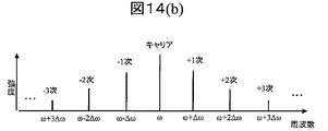
図14に光変調器の一例であるマッハツェンダ型光導波路強度変調器を示す。図14(a)に示すように入力ポートから入射した光は2分岐され,一方の導波路に入射した光はそのまま通過し,もう一方の導波路に入射した光に対しては,素子に電圧を加えることにより光路中の屈折率変化を与えることによって,位相変調がかけられる。両導波路を通過した光が合流すると,位相差によって強めあったり弱めあったりするため,光強度に変調を加えることができる。図14(b)に光変調器を通過した後の光スペクトルを示す。光変調器に加える電圧の変調周波数をdωとすると,入射する連続光の周波数ωに対して,ω±dωの±1次の成分,ω±2dωの±2次の成分,ω±3dωの±3次の成分と連続光の周波数に対してサイドバンドが生じる。各次数のサイドバンド強度は光変調器に加えるバイアス電圧を変えることによって調整可能である。
図15に光変調器を用いた高精度距離計測装置の構成図を示す。光源1501からは連続光が照射され変調用の光変調器1502に入射される。発振器1505から周波数fの電圧変調を光変調器1502にかけることによって,入射した光に対して,周波数f のn倍の周波数変調nfを与えることができる。光変調器1502を通過した光はファイバコリメータ107により,空間中に伝播し,偏光ビームスプリッタ108,λ/4板109を通過し,対象物110に照射される。反射光は再度λ/4板109,偏光ビームスプリッタ108を通過し,復調用の光変調器1503に入射される。発振器1506から復調用の光変調器に加える電圧の変調周波数をf+dfとすると,n倍の周波数変調nf+ndfを光に与えることができ,変調用の光変調器で加えた変調周波数との差周波数であるndfの変調周波数成分が射出される。よって,dfとして十分小さい値(数MHz~数kHz)を選べば,周波数応答の遅い検出器1504によって,高精度な距離計測が可能となる。また加える電圧の変調周波数のn倍の変調信号を使うので,発振器の周波数のn倍の精度で距離計測が可能となる。
一方、図15に示す距離計測装置は,光源1501からの連続光が光変調器(1502、1503)を2度通ることになり、特に高次の周波数成分は減衰されやすい。従って、高次の周波数成分は強度を強くすることが困難であり,対象物が粗面や傾斜面のように反射光強度が弱い場合,光変調器によって変調,復調された高次の周波数成分の信号検出することが難しい。また変調用の発振器および復調用の発振器を用いており,電気的なクロストークが発生し,測定結果にサイクリックエラーが生じてしまうという問題点がある。
上記図11、図15に示す距離計測装置の問題点に鑑み、開発された実施例1における,光コムおよび光導波路強度変調器を用いて高精度に距離計測を行う方法について図1(a)、図1(b)を用いて説明する。
図1(a)は,本実施例の距離計測装置の構成図の例である。本実施例では、光源として、図11で説明した離散した複数の光周波数の光を発振する光コムを用いる。光コム発生器101から照射された光コムはファイバコリメータ107により空間中に照射され,偏光ビームスプリッタ108に入射する。一部はファイバコリメータ111で集光され,光導波路強度変調器112に入射し,主要な部分はλ/4板109を通過し,対象物110に照射される。対象物からの反射光は再び,λ/4板109を通過し,偏光ビームスプリッタ108により反射され,ファイバコリメータ115で集光されて光導波路強度変調器116に入射する。発振器103は周波数fの電気信号を発生させ,パワーデバイダ106により2分岐して,それぞれ光導波路強度変調器112,116に入力される。発振器103で発生する電気信号の周波数によって、光導波路強度変調器112,116で変調させる周波数が決まる。光導波路強度変調器112を通過した光は受光器113によって電気信号に変換され,フィルタ114によって距離計測に用いる周波数成分のみを抽出し,位相計119の参照信号として入力される。光導波路強度変調器116を通過した光も同様に受光器117によって電気信号に変換され,フィルタ118によって距離計測に用いる周波数成分のみを抽出し,位相計119の測定信号として入力される。位相計119によって位相を算出し,距離演算回路120によって距離を演算する。
図1(b)に光導波路強度変調器を用いて光コムを光ビートダウンする原理を示す。例えば、光コムの繰返し周波数(frep)を10.0001MHzとすると周波数上で10.0001MHz間隔にスペクトルが存在する。あるスペクトルから10000本離れたスペクトルの周波数間隔は100.001GHzとなる。このビート信号を距離計測に用いる場合を考える。例えば,基準信号発生器104により駆動される発振器103から光導波路強度変調器112、116に周波数変調を加え, 1次のサイドバンド成分を用いて光ビートダウンする場合を考える。発振器103の発振周波数として100GHzを与えると,あるスペクトルから10000本離れたスペクトルの周波数間隔を100.001GHzから1MHzまでビートダウンして受光器113で検出することが可能となる。また2次の成分を用いて光ビートダウンする場合を考えると,発振器103の発振周波数として50GHzを与え,同様にしてあるスペクトルから10000本離れたスペクトルの周波数間隔を100.001GHzから1MHzまでビートダウンして検出することが可能となる。同様にしてn次の成分を用いて光ビートダウンする場合を考えると,発振器の発振周波数として100/n GHzを与え,同様にしてあるスペクトルから10000本離れたスペクトルの周波数間隔を100.001GHzから1MHzまでビートダウンして検出することが可能となる。即ち、光導波路強度変調器112,116は、発振器103から入力された周波数のn倍の周波数の光変調(光ビートダウン)を行うことができる。また、高次のサイドバンド成分を用いて光ビートダウンできれば,発振器の発振周波数を低周波に抑えることが可能となる。さらに、光コム101から照射された光は、光導波路強度変調器112または光導波路強度変調器116を一度しか通過しないため、高次の周波数成分の減衰を最小限に抑えることができ、高次の周波数成分を高精度で検出することができる。
光コム101の発振周波数と発振器103の発振周波数には周波数揺らぎが含まれるため,光ビートダウンした信号の周波数が揺らぎ,位相測定精度に悪影響を与える可能性がある。本実施例では、光ビートダウン信号の周波数を一定に保つために発振器102を備える。光ビートダウンした信号と発振器102との位相比較を行い(例えばミキサ121によって位相比較が可能),エラー信号を光コム101の繰返し周波数制御機構に入力することにより,光ビートダウン信号の周波数が一定となるよう,光コムの繰返し周波数の制御を行う。このとき基準信号発生器104からの信号をパワーデバイダ105により2分岐し,それぞれ発振器103と102の外部リファレンス信号とすることにより2つの発振器間で位相同期を取る必要がある。これにより、光ビートダウンした信号の周波数の揺らぎを防止し、位相測定精度の低下を抑制することができる。
本実施例によれば、光源として光コム101を用い,光導波路強度変調器112、116を用いて光コム101の高周波ビート成分を光ビートダウンして,低周波にて位相検出することにより、装置コストを上げずに測定精度を高めることができる。
本発明の実施例2について図2(a)、図2(b)を用いて説明する。
本実施例では,光源として光コムを用いるのではなく,LD2本を用いる装置の例を説明する。図2(a)は、実施例2におけるLD2本を用いる装置を示す構成図の例である。図2(a)の装置のうち、既に説明した図1に示された同一の符号を付された構成と、同一の機能を有する部分については、説明を省略する。
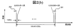
光源として発振周波数のわずかに異なるLD201とLD202を用いる。カップラ203によって同一光路となり,ファイバコリメータ107により空間中に照射され,偏光ビームスプリッタ108に入射する。一部はファイバコリメータ111で集光され,光導波路強度変調器112に入射し,主要な部分はλ/4板109を通過し,対象物110に照射される。対象物からの反射光は再び,λ/4板109を通過し,偏光ビームスプリッタ108により反射され,ファイバコリメータ115で集光されて光導波路強度変調器116に入射する。
図2(b)に光導波路強度変調器を用いてLD2本間のビート成分を光ビートダウンする原理を示す。例えば、LD間の周波数差を100.001GHzとする。このビート信号を距離計測に用いる場合を考える。例えば,発振器103から光導波路強度変調器に周波数変調を加え,1次のサイドバンド成分を用いて光ビートダウンする場合を考える。実施例1と同様にn次の成分を用いて光ビートダウンする場合を考えると,発振器103の発振周波数として100/n GHzを与え,1MHzまでビートダウンして検出することが可能となる。高次のサイドバンド成分を用いて光ビートダウンできれば,発振器の発振周波数を低周波に抑えることが可能となる。
LD2本間のビート周波数と発振器103の発振周波数には周波数揺らぎが含まれるため,光ビートダウンした信号の周波数が揺らぎ,位相測定精度に悪影響を与える可能性がある。光ビートダウン信号の周波数を一定に保つために発振器102を備える。光ビートダウンした信号と発振器102との位相比較を行い(例えばミキサ121によって位相比較が可能),エラー信号をLD201の発振周波数制御機構に入力することにより,光ビートダウン信号の周波数が一定となるよう,LD201の発振周波数の制御を行う。このとき基準信号発生器104からの信号をパワーデバイダ105により2分岐し,それぞれ発振器103と102の外部リファレンス信号とすることにより2つの発振器間で位相同期を取る必要がある。これにより、光ビートダウンした信号の周波数の揺らぎを防止し、位相測定精度の低下を抑制することができる。
本実施例によれば、光源として複数のLDを用いて,光導波路強度変調器を用いて複数のLD間の高周波ビート成分を光ビートダウンして,低周波にて位相検出することにより、装置コストを上げずに測定精度高めることができる。
また光コムを光源とした場合,距離計測に用いないビート信号も多数発生するが,LDの場合は距離計測に用いるビート信号のみ発生するため,フィルタによるビート信号の抽出が容易となる。
本発明の実施例3について図3(a)、図3(b)、図4(a)、図4(b)を用いて説明する。
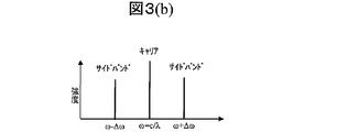
本実施例では,光変調器として光導波路強度変調器を用いるのではなく,電界吸収型強度変調器を用いる装置の例を説明する。図3(a)に電界吸収型強度変調器の原理について説明する。図3(a)に示すように連続光301を入射し,半導体素子306に照射する。半導体素子は加える電界によって,入射された波長に対して吸収率を変化させることが可能である。よって加える電界に変調をかけることによって,変調光302を得ることが可能となる。図3(b)に電界吸収型強度変調器を通過した後の光スペクトルを示す。光変調器に加える電圧の変調周波数をdωとすると,入射する連続光の周波数ωに対して,ω±dωのサイドバンドが生じる。図13に示した光導波路強度変調器では,位相変調を加えているため,変調周波数の±1次,±2次,±3次といったスペクトル成分が存在したが,電界吸収型強度変調器の場合は,吸収による強度変調のため,±1次のスペクトル成分しか存在しない。
図4(a)に電界吸収型強度変調器を用いた装置構成を示す。図4(a)の装置のうち、既に説明した図1に示された同一の符号を付された構成と、同一の機能を有する部分については、説明を省略する。光ビートダウンを行うために電界吸収型変調器401,402を用いる。また発振器103から加える周波数fのn倍の周波数で光ビートダウンを行うことを目的に電界吸収型変調器から射出した光を再度電界吸収型変調器に401,402入射させるファイバループを備える。またファイバループ中には光の減衰を抑えるために光アンプ404を導入する。
光コム発生器101から照射された光コムはファイバコリメータ107により空間中に照射され,偏光ビームスプリッタ108に入射する。一部はファイバコリメータ111で集光され,電界吸収型変調器401に入射し,主要な部分はλ/4板109を通過し,対象物110に照射される。対象物からの反射光は再び,λ/4板109を通過し,偏光ビームスプリッタ108により反射され,ファイバコリメータ115で集光されて電界吸収型変調器402に入射する。
図4(b)に電界吸収型強度変調器を用いて光コムを光ビートダウンする原理を示す。例えば、光コムの繰返し周波数を10.0001MHzとすると周波数上で10.0001MHz間隔にスペクトルが存在する。あるスペクトルから10000本離れたスペクトルの周波数間隔は100.001GHzとなる。このビート信号を距離計測に用いる場合を考える。例えば,電界吸収型強度変調器401,402を1回通過した周波数成分を用いて光ビートダウンする場合を考える。発振器103の発振周波数として100GHzを与え1MHzまでビートダウンして受光器113で検出することが可能となる。また電界吸収型強度変調器を2回通過した成分を用いて光ビートダウンする場合を考えると,発振器103の発振周波数として50GHzを与え,1MHzまでビートダウンして検出することが可能となる。同様にして電界吸収型強度変調器をn回通過した成分を用いて光ビートダウンする場合を考えると,発振器103の発振周波数として100/n GHzを与え,1MHzまでビートダウンして検出することが可能となる。電界吸収型強度変調器を複数回通過した周波数成分を用いて光ビートダウンできれば,発振器の発振周波数を低周波に抑えることが可能となる。
本実施例では、実施例1と同様に光ビートダウンした信号と発振器102との位相比較を行い(例えばミキサ121によって位相比較が可能),エラー信号を光コム101の繰返し周波数制御機構に入力することにより,光ビートダウン信号の周波数が一定となるよう,光コムの繰返し周波数の制御を行う。これにより、光ビートダウンした信号の周波数の揺らぎを防止し、位相測定精度の低下を抑制することができる。
本実施例によれば、光源として光コムを用いて,電界吸収型変調器を用いて光コムの高周波ビート成分を光ビートダウンして,低周波にて位相検出することにより、装置コストを上げずに測定精度高めることができる。またファイバループ内に電界吸収型変調器を備えることにより,光導波路強度変調器を用いた場合同様に,変調周波数の高次成分による光ビートダウンが可能となる。
本発明の実施例4について図5(a)、図5(b)を用いて説明する。
本実施例では,光変調器として電界吸収型強度変調器を用い,光源として,LD2本を用いる装置の例を説明する。図5(a)は,実施例4における装置構成図の例である。図5(a)の装置のうち、既に説明した図1に示された同一の符号を付された構成と、同一の機能を有する部分については、説明を省略する。
光源として発振周波数のわずかに異なるLD201とLD202を用いる。カップラ203によって同一光路となり,ファイバコリメータ107により空間中に照射され,偏光ビームスプリッタ108に入射する。一部はファイバコリメータ111で集光され,電界吸収型強度変調器401に入射し,主要な部分はλ/4板109を通過し,対象物110に照射される。対象物からの反射光は再び,λ/4板109を通過し,偏光ビームスプリッタ108により反射され,ファイバコリメータ115で集光されて電界吸収型強度変調器402に入射する。
図5(b)に電界吸収型強度変調器を用いてLD2本間のビート成分を光ビートダウンする原理を示す。例えば、LD間の周波数差を100.001GHzとする。このビート信号を距離計測に用いる場合を考える。実施例3と同様にして電界吸収型強度変調器をn回通過した成分を用いて光ビートダウンする場合を考えると,発振器の発振周波数として100/n GHzを与え,1MHzまでビートダウンして検出することが可能となる。電界吸収型強度変調器を複数回通過した周波数成分を用いて光ビートダウンできれば,発振器の発振周波数を低周波に抑えることが可能となる。
本実施例では、実施例2と同様に光ビートダウンした信号と発振器102との位相比較を行い(例えばミキサ121によって位相比較が可能),エラー信号を光コム101の繰返し周波数制御機構に入力することにより,光ビートダウン信号の周波数が一定となるよう,LD201のLD202との差周波数の制御を行う。これにより、光ビートダウンした信号の周波数の揺らぎを防止し、位相測定精度の低下を抑制することができる。
本実施例によれば、光源として複数のLDを用いて,電界吸収型変調器を用いて複数のLD間の高周波ビート成分を光ビートダウンして,低周波にて位相検出することにより、装置コストを上げずに測定精度高めることができる。
また光コムを光源とした場合,距離計測に用いないビート信号も多数発生するが,LDの場合は距離計測に用いるビート信号のみ発生するため,フィルタによるビート信号の抽出が容易となる。またファイバループ内に電界吸収型変調器を備えることにより,光導波路強度変調器を用いた場合同様に,変調周波数の高次成分による光ビートダウンが可能となる。
本発明の実施例5について図6(a)、図6(b)を用いて説明する。
本実施例では,複数の周波数の位相を測定し,長距離を高精度に測定する装置の例を説明する。図6(a)は,本実施例の距離計測装置の構成図の例である。図6(a)の装置のうち、既に説明した図1に示された同一の符号を付された構成と、同一の機能を有する部分については、説明を省略する。受光器113で検出されるビート成分には光コムの繰返し周波数の整数倍のビート成分および,光導波路強度変調器によって光ビートダウンしたビート成分が含まれる。例えば、,図6(b)に示すように光コムの繰返し周波数を10.0001MHz,光導波路強度変調器にて光ビートダウンする周波数を100GHzとすると,10.0001MHz間隔でビートが存在し,また10000本離れたスペクトル(周波数間隔100.001GHz)が光ビートダウンされた1MHzのビート成分も存在する。これらのビート成分を含む信号に対して,パワーデバイダ601によって3分岐し,それぞれバンドパスフィルタ603,605,607によって測定したい周波数成分を抽出する。例えば、バンドパスフィルタ603の通過中心周波数を1MHz,バンドパスフィルタ605の通過中心周波数を10MHz,バンドパスフィルタ603の通過中心周波数を1GHzとする。同様にして,受光器117の信号に対してパワーデバイダ602によって3分岐し,それぞれバンドパスフィルタ604,606,608によって測定したい周波数成分を抽出する。バンドパスフィルタ604,606,608の通過中心周波数はそれぞれ,1MHz,10MHz, 1GHzとする。位相計609によって1MHzの位相測定を行い,位相計610によって10MHzの位相測定を行い,位相計611によって1GHzの位相測定を行う。3つの位相情報から距離演算回路120によって距離計測を行う。各位相測定精度が2π/150以下とすると,周波数10MHzのビート成分は距離計測周期15mであり,距離計測精度は100mm(15mの1/150)となる。また周波数1GHzのビート成分は距離計測周期150mmであり,位相測定精度は1mm(150mmの1/150)となる。また周波数1MHzのビート成分(100.001GHzを光ビートダウンした成分)は距離計測周期1.5mmであり,位相測定精度は10um(1.5mmの1/150)となる。よって,15mの距離を精度10umにて距離計測が可能となる。
本実施例では、実施例1と同様に光ビートダウンした信号と発振器102との位相比較を行い(例えばミキサ121によって位相比較が可能),エラー信号を光コム101の繰返し周波数制御機構に入力することにより,光ビートダウン信号の周波数が一定となるよう,光コムの繰返し周波数の制御を行う。これにより、光ビートダウンした信号の周波数の揺らぎを防止し、位相測定精度の低下を抑制することができる。
本実施例によれば、光源として光コムを用いて,光導波路強度変調器を用いて光コムの高周波ビート成分を光ビートダウンして,低周波にて位相検出することにより、装置コストを上げずに測定精度高めることができる。また複数の周波数成分を用いることにより,長距離を高精度に測定することが可能となる。
本発明の実施例6について図7(a)、図7(b)を用いて説明する。
本実施例では,複数の周波数の位相を測定し,長距離を高精度に測定する装置の例であり,光源としてLDを複数本用いる例を説明する。図7(a)の装置のうち、既に説明した図2,図6に示された同一の符号を付された構成と、同一の機能を有する部分については、説明を省略する。図2ではLDを2本用いて差周波数のビートを距離計測に用いていたが,本実施例ではLDを複数本用いることによって,複数のビートを生じさせることが可能となる。例えば、LDを4本用いて,3種類のビートを生じさせる場合について説明する。図7(b)に示すように,基準とするLD202に対して,差周波数が10MHz,1GHz,100.001GHzとなるようにLD701,LD702,LD201を設定する。LD201のビート周波数は光導波路強度変調器によって1MHzまで光ビートダウンされる。受光器113,受光器117で検出されるビート周波数は1MHz,10MHz,1GHzとなる。これらのビート信号に対して,実施例5で説明したように,パワーデバイダ,バンドパスフィルタ,位相計,距離演算回路を用いることによって,15mの距離を精度10μmにて距離計測が可能となる。
LD201とLD202との差周波を光ビートダウンした信号の周波数を一定に保つために発振器102を備えている。光ビートダウンした信号をパワーデバイダ612によって抽出し,発振器102との位相比較を行い(例えばミキサ121によって位相比較が可能),エラー信号をLDの発振周波数制御機構に入力することにより,光ビートダウン信号の周波数が一定となるよう,LDの発振周波数の制御を行う。同様にして,LD202とLD701の差周波数を一定に保つために発振器705を備え,パワーデバイダ613によって抽出した信号と,発振器705との位相比較を行い,エラー信号をLD701の発振周波数制御機構に入力することにより,LD202とLD701の差周波数を一定に保つ。同様にして,LD202とLD702の差周波数を一定に保つために発振器706を備え,パワーデバイダ614によって抽出した信号と,発振器706との位相比較を行い,エラー信号をLD701の発振周波数制御機構に入力することにより,LD202とLD702の差周波数を一定に保つ。これにより、光ビートダウンした信号の周波数の揺らぎを防止し、位相測定精度の低下を抑制することができる。
本実施例によれば、光源として複数のLDを用いて,電界吸収型変調器を用いて複数のLD間の高周波ビート成分を光ビートダウンして,低周波にて位相検出することにより、装置コストを上げずに測定精度高めることができる。
また光コムと異なり,距離計測に用いないビート信号が発生しないため,フィルタによる抽出が容易となる。また複数の周波数成分を用いることにより,長距離を高精度に測定することが可能となる。
本発明の実施例7について図8を用いて説明する。
本実施例では,タイムオブフライト法と実施例5あるいは実施例6とを組み合わせて長距離を高精度に測定する装置の例を説明する。タイムオブフライト法とはパルス光を照射し,対象物に当たり,反射した光が受光器に検出される時間から対象物までの距離を測定する方法である。距離計測範囲に制約はなく(検出光強度に依存),距離計測精度は数mm程度である。実施例5あるいは6では長距離を距離計測する場合,距離計測用の物差しを多数用意する必要があるため,構成が大規模になってしまう。そこでタイムオブフライト法と組み合わせることによって,タイムオブフライト法にて長距離を数mm程度の精度で距離計測し,実施例5あるいは実施例6により,数mmを数十μmの精度で距離計測することが可能となる。図8は,本実施例の距離計測装置の構成図の例である。タイムオブフライト用光源801をカップラ203によって,光コムあるいはLDと同一光路にする。ファイバコリメータ107により空間中に照射され,偏光ビームスプリッタ108に入射し,λ/4板109を通過し,対象物110に照射される。対象物からの反射光は再び,λ/4板109を通過し,偏光ビームスプリッタ108により反射され,ビームスプリッタ803によって,タイムオブフライト用受光器802に入射する。タイムオブフライト用光源801から照射されるパルスの時間とタイムオブフライト用受光器802によって受光されるパルスの時間を距離演算回路804に入力する。照射パルスと受光パルスの時間差から距離をd=cΔt/2により算出する。ここでd:測定距離,c:光速,Δt:伝播時間(往復)となる。
本実施例では、実施例1と同様に光ビートダウンした信号と発振器102との位相比較を行い(例えばミキサ121によって位相比較が可能),エラー信号を光コム101の繰返し周波数制御機構に入力することにより,光ビートダウン信号の周波数が一定となるよう,光コムの繰返し周波数の制御を行う。これにより、光ビートダウンした信号の周波数の揺らぎを防止し、位相測定精度の低下を抑制することができる。
本実施例によれば、長距離を高精度に測距する場合において,複数物差しを備える必要がないため,装置の構成規模を小さく抑えることが可能となる。
本発明の実施例8について図9を用いて説明する。
本実施例では,実施例1から7で述べた距離計測光学系機構を搭載した3次元距離計測装置の例を説明する。図9は本実施例の装置構成図の例である。距離計測部903から照射される光はフォーカスレンズ902によって,対象物110にフォーカシングされる。これは対象物が粗面の場合,散乱により,距離計測部に戻る光が微弱となるため,フォーカシングすることによって検出するに十分な光量を得るためである。またガルバノスキャナ901によって3次元的にビーム走査可能となり,3次元形状計測が可能となる。ガルバノスキャナ,フォーカスレンズ,距離計測部を駆動するための電源ユニット904を備え,装置の制御および,距離計測結果を表示するために,GUIユニット905を備える。
本実施例によれば、フォーカシングにより,粗面に対しても十分な強度を得ることが可能となる。またガルバノスキャナによって3次元形状計測が可能となる。
本発明の実施例9について図10(a)、図10(b)、図10(c)を用いて説明する。
本実施例では,実施例2で述べたLD2本の差周波数を一定に保つための他の実施形態の例を説明する。図10は本実施例の装置構成図の例である。図10(a)は光導波路強度変調器1001を用いた一実施例である。LD201から照射される光を光導波路強度変調器1001に入射すると発振器1002の発振周波数fのn倍の変調周波数nf(n次サイドバンド)が生じる。サイドバンドのある周波数成分を光学的なフィルタで抽出し,LD202に入射することによって, LD202からは入射されたサイドバンド成分が増幅されて出力される(図10(c)参照)。これはインジェクションロックと呼ばれる方法で, LD間の周波数差を発振器の安定度で一定に保つことが可能となる。図10(b)は電界吸収型変調器を用いた一実施例である。LD201から照射される光を電界吸収型変調器に入射する。ファイバループによって電界吸収型変調器をn回通過した成分は発振周波数fのn倍の変調周波数nf(n次サイドバンド)が生じる。サイドバンドのある周波数成分を光学的なフィルタで抽出し,LD202に入射することによって,LD202からは入射されたサイドバンド成分が増幅されて出力される。
本実施例によれば、LD間の周波数差をエラー信号として制御するのではなく,LD間の周波数差を発振器の周波数安定性で一定に保つことが可能となるため,優れた安定を得ることができる。
これまで説明してきた実施例は、何れも本発明を実施するにあたっての具体化の一例を示したものに過ぎず、これらによって本発明の技術的範囲が限定的に解釈されない。すなわち、本発明はその技術思想、又はその主要な特徴から逸脱することなく、様々な形で実施することができる。また、実施例1乃至9を組み合わせることにより本発明を実施してもよい。
101…光コム,
102…発振器,
103…発振器,
104…基準信号,
105,106,122…パワーデバイダ,
107,111,115…ファイバコリメータ,
108…偏光ビームスプリッタ,
109…λ/4板,
110…測定対象物,
112,116…光導波路強度変調器,
113,117…受光器,
114,118…フィルタ,
119…位相計,
120…距離演算回路,
121…ミキサ,
201,202…LD,
203…カップラ,
301…連続光,
302…変調光,
303,304…レンズ,
305…抵抗,
306…半導体素子,
307…マイクロストリップライン,
308…高周波コネクタ,
401,402…電界吸収型変調器,
403,404…光アンプ,
601,602,612…パワーデバイダ,
603,604,605,606,607,608…バンドパスフィルタ,
609,610,611…位相計,
701,702…LD,
703,704…ミキサ,
705,706…発振器,
707,708,709…パワーデバイダ,
801…タイムフライト用光源,
802…タイムフライト用受光器,
803…ビームスプリッタ,
804…距離演算回路,
901…ガルバノスキャナ,
902…フォーカスレンズ,
903…距離計測部,
904…電源,
905…GUIユニット,
1001…光導波路強度変調器,
1002…発振器,
1003…電界吸収型変調器,
1004…光アンプ,
1201…光源,
1202…ビームスプリッタ,
1203,1204…受光器,
1205…測定対象物,
1301,1303…検出器,
1302,1304…ミキサ,
1501…光源,
1502,1503…光導波路強度変調器,
1504…検出器,
1505,1506…発振器,
1507,1508…パワーデバイダ,
1509…ミキサ,
1510…逓倍器
Claims (17)
- 複数の異なる周波数の光を発振する光源と、
前記光源から発振された光の周波数を変調する光変調器と、
基準信号発生器により駆動され、前記光変調器に電気信号を入力する発振器と、
前記光変調器により変調された光信号を電気信号に変換する受光器と、
前記受光器から出力された電気信号から距離を算出する距離演算回路とを備えることを特徴とする距離計測装置。 - 前記光源は所定の間隔で並んだ複数の周波数の光を有する光コムであることを特徴とする請求項1に記載の距離計測装置。
- 前記光源は異なる周波数の光を発振する複数のLDであることを特徴とする請求項1に記載の距離計測装置。
- 前記発振器とは異なり、前記基準信号発生器により駆動される他の発振器と、
前記光変調器で変調され、前記受光器で変換された電気信号と、前記他の発振器からの電気信号との位相比較を行うミキサと、
前記ミキサからの信号を入力し、前記光源の周波数を制御する周波数制御機構とを備える請求項1に記載の距離計測装置。 - 前記光変調器は、前記発振器から入力される周波数のn倍の周波数の光変調を加える光導波路強度変調器であることを特徴とする請求項1に記載の距離計測装置。
- 前記光変調器は、入力された光を複数回通過させることにより前記発振器から入力される周波数のn倍の周波数の光変調を加える電界吸収型強度変調器であることを特徴とする請求項1に記載の距離計測装置。
- 前記検出器によって検出された信号に含まれる周波数成分から所定の周波数成分を抽出する複数のバンドパスフィルタ備えることを特徴とする請求項1に記載の距離計測装置。
- 測定対象にフォーカスするフォーカスレンズと,測定対象を走査可能なガルバノスキャナと、装置制御および測定結果を表示するGUI画面とを備えることを特徴とする請求項1に記載の距離計測装置。
- 前記複数のLDの間に配置される他の変調器と、
前記他の変調器に電圧信号を入力する他の発信機とを備える請求項3に記載の距離計測装置。 - 光源から複数の異なる周波数の光を発振して測定対象に照射し,
前記光源からの光と測定対象から反射された光との周波数を発振器によって駆動される変調器により変調し,
変調された光信号を電気信号に変換し,
前記測定対象から反射された光から変換された電気信号と発振された光から変換されたの電気信号の位相から距離を算出することを特徴とする距離計測方法。 - 前記光源は、所定の間隔で並んだ複数の周波数の光を有する光コムであることを特徴とする請求項10に記載の距離計測方法。
- 前記光源は異なる周波数の光を発振する複数のLDであることを特徴とする請求項10に記載の距離計測方法。
- 前記変調器によって変調された光信号を電気信号に変換した際における周波数と、前記発振器とは異なる他の発振器からの電気信号との位相同期を取り、前記光源の発振周波数を制御することを特徴とする請求項10に記載の距離計測方法。
- 前記測定対象から反射された光と発振された光の周波数のn倍の周波数の光変調を加えることを特徴とする請求項10に記載の距離計測方法。
- 前記測定対象から反射された光と発振された光の周波数を電界吸収型変調器内を複数回通過させることにより、変調させることを特徴とする請求項10に記載の距離計測方法。
- 検出された信号に含まれる周波数成分から所定の複数の周波数成分を抽出することを特徴とする請求項10に記載の距離計測方法。
- 前記複数のLDのうち、一方のLDから発振された光に光変調を加えてから他方のLDに入射し、LD間の周波数差を制御することを特徴とする請求項12に記載の距離計測方法。
Priority Applications (1)
| Application Number | Priority Date | Filing Date | Title |
|---|---|---|---|
| EP12802335.5A EP2725385A4 (en) | 2011-06-23 | 2012-04-23 | DISTANCE METHOD AND DEVICE |
Applications Claiming Priority (2)
| Application Number | Priority Date | Filing Date | Title |
|---|---|---|---|
| JP2011139056A JP5736247B2 (ja) | 2011-06-23 | 2011-06-23 | 距離計測方法および装置 |
| JP2011-139056 | 2011-06-23 |
Publications (1)
| Publication Number | Publication Date |
|---|---|
| WO2012176366A1 true WO2012176366A1 (ja) | 2012-12-27 |
Family
ID=47422231
Family Applications (1)
| Application Number | Title | Priority Date | Filing Date |
|---|---|---|---|
| PCT/JP2012/002767 WO2012176366A1 (ja) | 2011-06-23 | 2012-04-23 | 距離計測方法および装置 |
Country Status (3)
| Country | Link |
|---|---|
| EP (1) | EP2725385A4 (ja) |
| JP (1) | JP5736247B2 (ja) |
| WO (1) | WO2012176366A1 (ja) |
Cited By (2)
| Publication number | Priority date | Publication date | Assignee | Title |
|---|---|---|---|---|
| CN112180390A (zh) * | 2020-09-18 | 2021-01-05 | 常州大学 | 一种测距装置和方法 |
| WO2022209008A1 (ja) * | 2021-03-29 | 2022-10-06 | 株式会社Xtia | 光コム発生装置 |
Families Citing this family (6)
| Publication number | Priority date | Publication date | Assignee | Title |
|---|---|---|---|---|
| KR101670474B1 (ko) * | 2013-03-22 | 2016-10-28 | 광주과학기술원 | 광학 장치 및 이의 동작 방법 |
| JPWO2014203654A1 (ja) * | 2013-06-17 | 2017-02-23 | 株式会社日立製作所 | 距離測定装置、形状測定装置、加工システム、距離測定方法、形状測定方法および加工方法 |
| KR102292436B1 (ko) * | 2016-03-31 | 2021-08-20 | 아이피지 포토닉스 코포레이션 | 강도 펄스 형상 보정을 이용하는 초고속 펄스 레이저 시스템 |
| JP6902902B2 (ja) * | 2017-03-30 | 2021-07-14 | 株式会社トプコン | 光波距離計 |
| JP6902901B2 (ja) * | 2017-03-30 | 2021-07-14 | 株式会社トプコン | 光波距離計 |
| JP7448962B2 (ja) | 2021-06-17 | 2024-03-13 | 株式会社OptoComb | 光コム距離計測用の光コム発生装置 |
Citations (5)
| Publication number | Priority date | Publication date | Assignee | Title |
|---|---|---|---|---|
| JPS4619180Y1 (ja) * | 1970-02-26 | 1971-07-03 | ||
| JPH09199778A (ja) * | 1996-01-17 | 1997-07-31 | Atr Hikari Denpa Tsushin Kenkiyushiyo:Kk | 半導体電界吸収型光変調装置 |
| JP3089376B2 (ja) | 1992-09-11 | 2000-09-18 | 工業技術院長 | 距離測定装置 |
| JP2006184181A (ja) | 2004-12-28 | 2006-07-13 | National Institute Of Advanced Industrial & Technology | 距離測定装置 |
| JP2011080860A (ja) * | 2009-10-07 | 2011-04-21 | Toyota Central R&D Labs Inc | テラヘルツレーダ装置 |
Family Cites Families (3)
| Publication number | Priority date | Publication date | Assignee | Title |
|---|---|---|---|---|
| JP3854656B2 (ja) * | 1996-03-01 | 2006-12-06 | 住友大阪セメント株式会社 | 光強度変調器及び光波距離計 |
| FR2757640B1 (fr) * | 1996-12-24 | 1999-04-09 | Thomson Csf | Systeme optique de mesure de vitesse et/ou de distance d'objet |
| JP5511162B2 (ja) * | 2008-07-31 | 2014-06-04 | 株式会社ミツトヨ | 多波長干渉変位測定方法及び装置 |
-
2011
- 2011-06-23 JP JP2011139056A patent/JP5736247B2/ja not_active Expired - Fee Related
-
2012
- 2012-04-23 WO PCT/JP2012/002767 patent/WO2012176366A1/ja active Application Filing
- 2012-04-23 EP EP12802335.5A patent/EP2725385A4/en not_active Withdrawn
Patent Citations (5)
| Publication number | Priority date | Publication date | Assignee | Title |
|---|---|---|---|---|
| JPS4619180Y1 (ja) * | 1970-02-26 | 1971-07-03 | ||
| JP3089376B2 (ja) | 1992-09-11 | 2000-09-18 | 工業技術院長 | 距離測定装置 |
| JPH09199778A (ja) * | 1996-01-17 | 1997-07-31 | Atr Hikari Denpa Tsushin Kenkiyushiyo:Kk | 半導体電界吸収型光変調装置 |
| JP2006184181A (ja) | 2004-12-28 | 2006-07-13 | National Institute Of Advanced Industrial & Technology | 距離測定装置 |
| JP2011080860A (ja) * | 2009-10-07 | 2011-04-21 | Toyota Central R&D Labs Inc | テラヘルツレーダ装置 |
Non-Patent Citations (1)
| Title |
|---|
| See also references of EP2725385A4 * |
Cited By (3)
| Publication number | Priority date | Publication date | Assignee | Title |
|---|---|---|---|---|
| CN112180390A (zh) * | 2020-09-18 | 2021-01-05 | 常州大学 | 一种测距装置和方法 |
| CN112180390B (zh) * | 2020-09-18 | 2022-05-06 | 常州大学 | 一种测距装置和方法 |
| WO2022209008A1 (ja) * | 2021-03-29 | 2022-10-06 | 株式会社Xtia | 光コム発生装置 |
Also Published As
| Publication number | Publication date |
|---|---|
| JP2013007591A (ja) | 2013-01-10 |
| EP2725385A4 (en) | 2015-04-01 |
| JP5736247B2 (ja) | 2015-06-17 |
| EP2725385A1 (en) | 2014-04-30 |
Similar Documents
| Publication | Publication Date | Title |
|---|---|---|
| JP5736247B2 (ja) | 距離計測方法および装置 | |
| Zou et al. | Microwave frequency measurement based on optical power monitoring using a complementary optical filter pair | |
| JP5254844B2 (ja) | 距離測定装置 | |
| WO2010001809A1 (ja) | 距離計及び距離測定方法並びに光学的三次元形状測定機 | |
| US8692981B2 (en) | Evaluation device, measuring arrangement and method for path length measurement | |
| WO2018170478A1 (en) | Fmcw lidar methods and apparatuses including examples having feedback loops | |
| EP3410185A1 (en) | Optical dual-comb source apparatuses including optical microresonator | |
| WO2014203654A1 (ja) | 距離測定装置、形状測定装置、加工システム、距離測定方法、形状測定方法および加工方法 | |
| JP2010203877A (ja) | 距離測定装置 | |
| JP6019360B2 (ja) | 光ヘテロダイン距離計 | |
| JP2011181691A (ja) | パルスレーザ、光周波数安定化レーザ、測定装置および測定方法 | |
| US20210190474A1 (en) | Laser apparatus, measurement system, and measurement method | |
| JP2020012641A (ja) | 距離計及び距離測定方法並びに光学的三次元形状測定機 | |
| US20230194683A1 (en) | Interferometric dual-comb distance measuring device and measuring method | |
| JP4617434B2 (ja) | 距離測定装置 | |
| JP6264547B2 (ja) | 光信号生成装置、距離測定装置、分光特性測定装置、周波数特性測定装置及び光信号生成方法 | |
| JP5421013B2 (ja) | 位置決め装置及び位置決め方法 | |
| WO2014045655A1 (ja) | 距離計測方法および装置 | |
| JP2014149190A (ja) | 計測装置、計測方法、光源装置および物品の製造方法 | |
| KR101684269B1 (ko) | 프리러닝 펨토초 레이저 기반의 실시간 합성파 결정을 이용한 거리측정 장치 | |
| JP6961185B1 (ja) | 光コム発生器制御装置 | |
| KR102360033B1 (ko) | 미소 광 공진기를 구비하는 이중 광빗 광원 장치 | |
| US20220268931A1 (en) | Measurement apparatus and measurement method | |
| US11879975B2 (en) | Measurement apparatus and measurement method | |
| Yang et al. | Long-distance measurement applying two high-stability and synchronous wavelengths |
Legal Events
| Date | Code | Title | Description |
|---|---|---|---|
| 121 | Ep: the epo has been informed by wipo that ep was designated in this application |
Ref document number: 12802335 Country of ref document: EP Kind code of ref document: A1 |
|
| REEP | Request for entry into the european phase |
Ref document number: 2012802335 Country of ref document: EP |
|
| WWE | Wipo information: entry into national phase |
Ref document number: 2012802335 Country of ref document: EP |
|
| NENP | Non-entry into the national phase |
Ref country code: DE |