WO2012176330A1 - 半導体装置 - Google Patents
半導体装置 Download PDFInfo
- Publication number
- WO2012176330A1 WO2012176330A1 PCT/JP2011/064542 JP2011064542W WO2012176330A1 WO 2012176330 A1 WO2012176330 A1 WO 2012176330A1 JP 2011064542 W JP2011064542 W JP 2011064542W WO 2012176330 A1 WO2012176330 A1 WO 2012176330A1
- Authority
- WO
- WIPO (PCT)
- Prior art keywords
- signal
- semiconductor device
- signals
- electrode
- external terminals
- Prior art date
- Legal status (The legal status is an assumption and is not a legal conclusion. Google has not performed a legal analysis and makes no representation as to the accuracy of the status listed.)
- Ceased
Links
Images








Classifications
-
- G—PHYSICS
- G06—COMPUTING OR CALCULATING; COUNTING
- G06F—ELECTRIC DIGITAL DATA PROCESSING
- G06F13/00—Interconnection of, or transfer of information or other signals between, memories, input/output devices or central processing units
- G06F13/14—Handling requests for interconnection or transfer
- G06F13/16—Handling requests for interconnection or transfer for access to memory bus
- G06F13/1668—Details of memory controller
- G06F13/1684—Details of memory controller using multiple buses
Definitions
- the present invention relates to a semiconductor device, and more particularly to a semiconductor device connected to a semiconductor memory device through a plurality of wirings.
- Semiconductor memory devices such as DRAM (Dynamic Random Access Memory) and SRAM (Static Random Access Memory) are semiconductor memory chips mounted on the surface of the package substrate and sealed with resin.
- the external terminals are arranged in a matrix.
- a semiconductor memory chip has a plurality of memory cells, write / read circuits, etc. formed on the surface of a semiconductor substrate, and is connected to a plurality of external terminals via a package substrate.
- the arrangement pattern of the external terminals of the semiconductor memory device differs depending on the type of the semiconductor memory device (see, for example, JP-A-2003-51545 (Patent Document 1)).
- a semiconductor device that controls such a semiconductor memory device is a semiconductor chip mounted on the surface of a package substrate and sealed with resin, and a plurality of external terminals are arranged in a matrix on the back surface of the package substrate.
- the semiconductor chip has a memory controller or the like formed on the surface of a semiconductor substrate, and is connected to a plurality of external terminals via a package substrate.
- the arrangement pattern of the external terminals of the semiconductor device is set according to the arrangement pattern of the external terminals of the semiconductor memory device.
- the semiconductor memory device and the semiconductor device are mounted on one motherboard to constitute one semiconductor module.
- Each external terminal of the semiconductor memory device is connected to a corresponding external terminal of the semiconductor device via a wiring of the mother board (see, for example, JP 2010-123203 A (Patent Document 2)).
- the semiconductor device When a semiconductor module is configured by mounting a semiconductor device and one or more semiconductor memory devices on a single motherboard, the semiconductor device is adapted to the model and number of semiconductor memory devices so that the wiring of the motherboard does not cross each other. It is necessary to optimally design the arrangement pattern of external terminals. However, if the arrangement pattern of the external terminals of the semiconductor device is changed each time the model or number of the semiconductor memory device is changed, there is a problem that the cost of the semiconductor device increases.
- a main object of the present invention is to provide a low-cost semiconductor device.
- the semiconductor device outputs N (where N is an integer larger than M) signals divided in advance into M (where M is an integer equal to or greater than 2) signal groups.
- Each signal group includes a plurality of signals, and each buffer group includes the same number of buffer circuits as the signals of the corresponding signal group.
- Each switching circuit applies the plurality of signals of the corresponding signal group in parallel to the plurality of buffer circuits of the corresponding buffer group in the order corresponding to the mode setting signal.
- Each buffer circuit of each buffer group applies a signal supplied from a corresponding switching circuit to a corresponding external terminal.
- the switching circuit applies the plurality of signals generated by the signal generation circuit in parallel to the plurality of buffer circuits in the order corresponding to the mode setting signal. Therefore, since the arrangement pattern of the external terminals can be switched according to the type and number of semiconductor memory devices to be connected, the cost of the device can be reduced.
- FIG. 2 is a block diagram showing a configuration of a semiconductor chip included in the semiconductor device shown in FIG. 1.
- FIG. 5 is a block diagram illustrating a configuration of a signal input / output circuit illustrated in FIG. 4.
- FIG. 6 is a block diagram showing a configuration of a buffer circuit B1 shown in FIG.
- FIG. 6 is a block diagram showing a configuration of a buffer circuit B3 shown in FIG. FIG.
- FIG. 6 is a block diagram showing a configuration of a buffer circuit B4 shown in FIG.
- FIG. 3 is a diagram showing an arrangement pattern of external terminals in a first mode and a second mode of the semiconductor device shown in FIG. 1.
- 10 is a time chart showing the waveform of the signal shown in FIG. 9.
- 2 is a flowchart showing an operation of the semiconductor device shown in FIG.
- FIG. 2 is a diagram showing an arrangement pattern of external terminals in a first mode of the semiconductor device shown in FIG. 1.
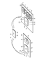
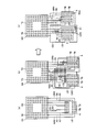
- FIG. 2 is a diagram showing an arrangement pattern of external terminals of the semiconductor memory device 3 shown in FIG. 1. It is a figure which shows the 1st layer of the motherboard 4 shown in FIG. It is a figure which shows the 3rd layer of the motherboard 4 shown in FIG.
- FIG. 4 is a diagram showing an arrangement pattern of external terminals in a second mode of the semiconductor device shown in FIG. 1.
- FIG. 2 is a diagram showing an arrangement pattern of external terminals of the semiconductor memory device 6 shown in FIG. 1. It is a figure which shows the 1st layer of the motherboard 7 shown in FIG. It is a figure which shows the 3rd layer of the motherboard 7 shown in FIG. It is a figure which shows the 6th layer of the motherboard 7 shown in FIG. It is a figure which shows the structure and usage method of the semiconductor device by Embodiment 2 of this invention. It is a figure which shows the effect of the semiconductor device shown in FIG.
- FIG. 1A is a diagram showing a configuration of a semiconductor device (LSI: Large Scale Integration) 1 according to Embodiment 1 of the present invention, and FIGS. FIG.
- LSI Large Scale Integration
- a semiconductor device 1 has a semiconductor chip mounted on the surface of a package substrate and sealed with resin, and a plurality of external terminals TA are arranged in a matrix on the back surface of the package substrate. Yes.
- the semiconductor chip has a memory controller or the like formed on the surface of a semiconductor substrate, and is connected to a plurality of external terminals TA through a package substrate.
- the semiconductor module 2 is obtained by mounting the semiconductor device 1 and the two semiconductor memory devices 3 on the surface of one motherboard 4.
- the semiconductor memory device 3 is, for example, a DDR3-SDRAM (Double Data Rate3-Synchronous Dynamic Random Access Memory).
- the semiconductor memory device 3 has semiconductor memory chips mounted on the front surface of a package substrate and sealed with resin, and a plurality of external terminals TB are arranged in a matrix on the back surface of the package substrate.
- the semiconductor memory chip has a plurality of memory cells, write / read circuits, etc. formed on the surface of a semiconductor substrate, and is connected to a plurality of external terminals TB via a package substrate.
- the plurality of external terminals TB of the semiconductor memory device 3 are arranged according to a predetermined arrangement pattern.
- the arrangement pattern of the external terminals TB of the semiconductor memory device 3 is fixed. That is, the type of signal input to each external terminal TB is fixed.
- the arrangement pattern of the external terminals TA of the semiconductor device 1 is set according to the arrangement pattern of the external terminals TB of the semiconductor memory device 3 by a built-in switching circuit. That is, the type of signal output from each external terminal TA can be changed by the switching circuit.
- the switching circuit will be described later.
- the mother board 4 is formed with a plurality of wirings for connecting a plurality of external terminals TA of the semiconductor device 1 and a plurality of external terminals TB of the semiconductor memory device 3.
- the arrangement pattern of the external terminals TA of the semiconductor device 1 is set so that the wirings of the mother board 4 do not intersect in the same layer.
- Each external terminal TB of the semiconductor memory device 3 is connected to a corresponding external terminal TA of the semiconductor device 1 through wiring of the mother board 4.
- the semiconductor module 5 is obtained by mounting the semiconductor device 1 and the two semiconductor memory devices 6 on the surface of one motherboard 7.
- the semiconductor memory device 6 is a different type of semiconductor memory device from the semiconductor memory device 3, and is, for example, a DDR2-SDRAM.
- the semiconductor memory device 6 is a semiconductor memory chip mounted on the surface of a package substrate and sealed with resin, and a plurality of external terminals TC are arranged in a matrix on the back surface of the package substrate.
- the semiconductor memory chip has a plurality of memory cells, write / read circuits, etc. formed on the surface of a semiconductor substrate, and is connected to a plurality of external terminals TC via a package substrate.
- the plurality of external terminals TC of the semiconductor memory device 6 are arranged according to a predetermined arrangement pattern.
- the arrangement pattern of the external terminals TC of the semiconductor memory device 6 is fixed and is different from the arrangement pattern of the external terminals TB of the semiconductor memory device 3.
- the arrangement pattern of the external terminals TA of the semiconductor device 1 is set according to the arrangement pattern of the external terminals TC of the semiconductor memory device 6 by a built-in switching circuit.
- a plurality of wirings for connecting the plurality of external terminals TA of the semiconductor device 1 and the plurality of external terminals TC of the semiconductor memory device 6 are formed on the mother board 7.
- the arrangement pattern of the external terminals TA of the semiconductor device 1 is set so that the wirings of the mother board 7 do not cross each other.
- Each external terminal TC of the semiconductor memory device 6 is connected to a corresponding external terminal TA of the semiconductor device 1 through wiring of the mother board 7.
- the pattern arrangement of the external terminals TA of the semiconductor device 1 can be changed according to the model of the semiconductor memory device to be connected, so that the cost of the device and the signal transmission characteristics can be reduced. Improvements can be made.
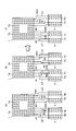
- FIGS. 2A to 2C are diagrams showing the effects of the first embodiment.
- FIG. 2A is a view of the semiconductor device 1 and the two semiconductor memory devices 3 as seen from the back side.
- a plurality of external terminals TA are arranged in a matrix on the rectangular back surface of the semiconductor device 1.
- a plurality of external terminals TB are arranged in a matrix on the rectangular back surface of each semiconductor memory device 3.
- One side of the semiconductor device 1 and one side of the two semiconductor memory devices 3 are arranged to face each other.
- eight external terminals TA for the signals A1, A2, RAS0, CAS0, A5, A6, RAS1, CAS1 are provided along one side of the semiconductor device 1 opposite to one side of the two semiconductor memory devices 3. If provided, the eight external terminals TA of the semiconductor device 1 and the total of eight external terminals TB of the two semiconductor memory devices 3 can be connected by eight wirings LB that do not cross each other.
- FIG. 2B is a view of the semiconductor device 1 and the two semiconductor memory devices 6 as seen from the back side.
- a plurality of external terminals TA are arranged in a matrix on the rectangular back surface of the semiconductor device 1.
- a plurality of external terminals TC are arranged in a matrix on the rectangular back surface of each semiconductor memory device 6.
- One side of the semiconductor device 1 and one side of the two semiconductor memory devices 6 are arranged to face each other.
- the arrangement pattern shown in FIG. 2A is adopted as the arrangement pattern of the external terminals TA of the semiconductor device 1, and each external terminal TA of the semiconductor device 1 is connected to the corresponding external terminal TC via the wiring LC.
- the eight wirings LC intersect at four places.
- the built-in switching circuit causes the external terminal TA of the semiconductor device 1 to be connected. Since the arrangement pattern is changed according to the external terminal TC of the semiconductor memory device 6, the crossing of the wiring LC can be eliminated.
- the semiconductor device 1 when the semiconductor module 2 is configured by the semiconductor device 1 and the two semiconductor memory devices 3, the semiconductor device 1 is set to the first mode by the mode setting signal.
- the semiconductor device 1 set in the first mode outputs signals A1, A2, RAS0, CAS0, A5, A6, RAS1, and CAS1 from eight external terminals TA facing one side of the two semiconductor memory devices 3, respectively. To do. Therefore, the eight wirings LB can be formed on the mother board 4 without crossing.
- the semiconductor device 1 when the semiconductor module 5 is configured by the semiconductor device 1 and the two semiconductor memory devices 6, the semiconductor device 1 is set to the second mode by the mode setting signal.
- the semiconductor device 1 set to the second mode outputs signals A2, A1, CAS0, RAS0, A6, A5, CAS1, RAS1 from eight external terminals TA facing one side of the two semiconductor memory devices 6, respectively. To do. Therefore, the eight wirings LC can be formed on the mother board 7 without crossing.
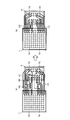
- 3A and 3B are views of the semiconductor device 1 and the semiconductor memory device 6 as seen from the back side, and are other views showing the effects of the first embodiment.
- 3A and 3B a plurality of external terminals TA of the semiconductor device 1 and a plurality of external terminals TC of the semiconductor memory device 6 are connected by a plurality of wirings LC.
- the plurality of wirings LC intersect at a plurality of locations.
- the two wirings LC cannot be formed in the same wiring layer, and one wiring LC is formed in another wiring layer, and the upper wiring LC and the lower wiring LC. Need to be connected via hole. Therefore, the number of wiring layers increases, resulting in an increase in cost.
- the signal is transmitted through a plurality of via holes, the transmission characteristics are deteriorated. Further, the layout area of the wiring LC increases.
- the semiconductor module 5 having a low cost, good transmission characteristics, and a small layout area can be configured.
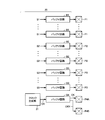
- FIG. 4 is a block diagram showing a configuration of the semiconductor chip 10 included in the semiconductor device 1.
- the semiconductor chip 10 includes a semiconductor substrate 11. On the semiconductor substrate 11, input terminals TI1, TI2, a plurality of pads P, a system controller (SYSC) 12, a bus 13, a memory controller 14, a selector 15, and a signal input / output circuit 20 are formed.
- system controller system controller
- the power-on reset signal POR is given to the input terminal TI1 from another semiconductor chip in the semiconductor device 1 or from outside the semiconductor device 1.
- the power-on reset signal POR is a signal that is activated only for a predetermined period when a power supply voltage is supplied to the semiconductor device 1.
- a mode setting signal MODE is externally applied to the input terminal TI2. For example, when semiconductor device 1 is set to the first mode, mode setting signal MODE is set to “L” level, and when semiconductor device 1 is set to the second mode, mode setting signal MODE is set to “H” level. Is done.
- Each pad P is connected to the package substrate via a bonding wire, for example, and further connected to a corresponding external terminal TA via wiring on the package substrate.
- the system controller 12 is reset when the power-on reset signal POR is set to the activation level, and controls the entire semiconductor chip 10 via the bus 13.
- the memory controller 14 generates a plurality of signals S for controlling the semiconductor memory device in accordance with signals given from the system controller 12 or the like via the bus 13.
- the plurality of signals S are divided in advance into three signal groups.
- Each of the plurality of signals S1 belonging to the first signal group may be set to any one of “H” level and “L” level when the semiconductor chip 10 is reset by the power-on reset signal POR or the like.
- the plurality of signals S1 are address signals A00 to A15 and bank address signals BA0 to BA2.
- Each of the plurality of signals S2 belonging to the second signal group is a signal to be forcibly set to “H” level when the semiconductor chip 10 is reset by the power-on reset signal POR or the like.
- the plurality of signals S2 are chip select signals CSN0 and CSN1, a write enable signal WEN, a column address strobe signal CASN, and a row address strobe signal RASN.
- Each of the plurality of signals S3 belonging to the third signal group is a signal that should be forcibly set to the “L” level when the semiconductor chip 10 is reset by the power-on reset signal POR or the like.
- the plurality of signals S3 are signals ODT0 and ODT1 and a clock enable signal CKE.
- the plurality of signals S1 in the first signal group, the plurality of signals S2 in the second signal group, and the plurality of signals S3 in the third signal group are supplied to the selector 15.
- the mode setting circuit 14a included in the memory controller 14 generates the selector control signal SE according to the mode setting signal MODE given from the outside via the input terminal TI2.
- the selector control signal SE is given to the selector 15.
- the selector 15 includes a register 16 and switching circuits 17-19.
- the register 16 holds the selector control signal SE from the mode setting circuit 14a and supplies the selector control signal SE to each of the switching circuits 17-19.
- the switching circuit 17 supplies a plurality of signals S1 from the memory controller 14 in parallel to the signal input / output circuit 20 in the order corresponding to the selector control signal SE from the register 16.
- the switching circuit 18 supplies a plurality of signals S2 from the memory controller 14 in parallel to the signal input / output circuit 20 in the order corresponding to the selector control signal SE from the register 16.
- the switching circuit 19 supplies a plurality of signals S3 from the memory controller 14 in parallel to the signal input / output circuit 20 in the order corresponding to the selector control signal SE from the register 16.
- the signal input / output circuit 20 transmits the plurality of signals S1, the plurality of signals S2, and the plurality of signals S3 given from the memory controller 14 via the selector 15 to the plurality of pads P, respectively. Further, the signal input / output circuit 20 generates clock signals CK and CKN and supplies them to the two pads P.
- the signal input / output circuit 20 includes a plurality of buffer circuits B1 provided corresponding to the plurality of signals S1 from the switching circuit 17, and a plurality of signals S2 from the switching circuit 18, respectively. Includes a plurality of buffer circuits B2 provided corresponding to the plurality of signals, a plurality of buffer circuits B3 provided corresponding to the plurality of signals S3 from the switching circuit 19, respectively, a clock generation unit 21, and a buffer circuit B4. .
- the plurality of pads P include a plurality of pads P1 corresponding to the plurality of buffer circuits B1, a plurality of pads P2 corresponding to the plurality of buffer circuits B2, respectively, and a plurality of pads P3 corresponding to the plurality of buffer circuits B3, respectively. And two pads P4A and P4B corresponding to the buffer circuit B4.
- Each buffer circuit B1 transmits the signal S1 from the switching circuit 17 to the corresponding pad P1.
- Each buffer circuit B2 transmits the signal S2 from the switching circuit 18 to the corresponding pad P2.
- Each buffer circuit B3 transmits the signal S3 from the switching circuit 19 to the corresponding pad P3.
- the clock generation unit 21 generates a clock signal CK.
- the buffer circuit B4 generates a complementary signal CKN of the clock signal CK in response to the clock signal CK from the clock generator 21, and applies the clock signals CK and CKN to the pads P4A and P4B, respectively.
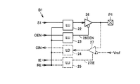
- the buffer circuit B1 corresponding to the signal S1 includes level-up shifters (LU) 22, 23, 25, a level-down shifter (LD) 24, a buffer 26, and a comparator 27, as shown in FIG.
- the power supply voltage of memory controller 14 is 1.0 V, for example, and the power supply voltage of semiconductor memory devices 3 and 6 is 1.5 V, for example.
- the level-up shifter 22 converts the logic amplitude voltage of the signal S1 from the memory controller 14 from 1.0V to 1.5V, and supplies it to the input node of the buffer 26. Further, when the reset signal RE is set to the “H” level of the activation level, the level up shifter 22 outputs the “H” level signal regardless of the logic level of the signal S1. When the power-on reset signal POR is activated, the reset signal RE is activated.
- the level-up shifter 23 converts the logic amplitude voltage of the output enable signal OEN from 1.0 V to 1.5 V, and supplies it to the control node of the buffer 26.
- the signal OEN is set to the “L” level of the activation level when the signal S1 is output to the outside, and is set to the “H” level of the inactivation level when the signal S1 is not output to the outside. Further, the level-up shifter 23 outputs the “L” level regardless of the logic level of the signal OEN when the reset signal RE is set to the “H” level of the activation level.
- the buffer 26 is driven at 1.5 V, which is the power supply voltage of the semiconductor memory devices 3 and 6.
- the buffer 26 outputs the signal S1 to the pad P1 when the output signal 26OEN of the level up shifter 23 is set to the activation level “L”, and the signal 26OEN is set to the deactivation level “H”.
- the pad P1 is set to a high impedance state. Therefore, when the reset signal RE is set to the activation level “H” level, the pad P1 is set to the “H” level regardless of the logic levels of the signals S1 and OEN.
- the level-down shifter 24, the level-up shifter 25, and the comparator 27 are used when testing the semiconductor device 1 before shipment, and are not normally used, and are indicated by dotted lines.
- the level-up shifter 25 converts the logic amplitude voltage of the input enable signal IE from 1.0 V to 1.5 V, and supplies it to the control node of the comparator 27.
- the signal IE is set to the activation level “H” level in the test mode, and is set to the deactivation level “L” level in the normal operation. Further, when the reset signal RE is set to the activation level “H” level, the level up shifter 25 outputs the “L” level regardless of the logic level of the signal IE.
- the comparator 27 is driven at 1.5 V, which is the power supply voltage of the semiconductor memory devices 3 and 6.
- the comparator 27 is activated when the output signal 27IE of the level-up shifter 25 is the “H” level of the activation level, and compares the voltage applied from the outside to the pad P1 and the reference voltage Vref, and compares them. A signal indicating the result is output.
- the output signal of the comparator 27 becomes “L” level.
- the output signal of comparator 27 is at “H” level.
- the level down shifter 24 converts the logic amplitude voltage of the output signal of the comparator 27 from 1.5V to 1.0V to generate the test signal CIN. Further, when the reset signal RE is set to the “H” level as the activation level, the level down shifter 24 outputs the “L” level regardless of the logic level of the signal IE.
- the configuration of the buffer circuit B2 corresponding to the signal S2 is the same as that of the buffer circuit B1 corresponding to the signal S1.
- Signal S2 is a signal to be set to "H” level when reset.
- the signal S1 may be either “H” level or “L” level when reset.
- the configuration of the semiconductor device 1 is simplified by configuring the buffer circuits B1 and B2 to have the same configuration.
- the buffer circuit B3 corresponding to the signal S3 is obtained by replacing the level up shifter 22 of the buffer circuit B1 with a level up shifter 28 as shown in FIG.
- the level-up shifter 28 converts the logic amplitude voltage of the signal S3 from the memory controller 14 from 1.0V to 1.5V and applies the converted voltage to the input node of the buffer 26. Further, when the reset signal RE is set to the “H” level of the activation level, the level up shifter 28 outputs the “L” level signal regardless of the logic level of the signal S3.
- the buffer circuit B4 is obtained by replacing the level-up shifter 22 of the buffer circuit B1 with a level-up shifter 29 and adding a buffer 30.
- the level-up shifter 29 converts the logic amplitude voltage of the clock signal CK from the clock generation unit 21 from 1.0 V to 1.5 V and applies the converted voltage to the input node of the buffer 26. Further, the level up shifter 29 generates a complementary signal CKN of the clock signal CK and supplies it to the input node of the buffer 30. The logic amplitude voltage of the signal CKN is 1.5V. Further, when the reset signal RE is set to the “H” level of the activation level, the level up shifter 29 sets the output clock signals CK and CKN to the “H” level regardless of the logic level of the input clock signal CK. And “L” level.
- the buffers 26 and 30 are driven at 1.5 V, which is the power supply voltage of the semiconductor memory devices 3 and 6.
- the buffer 26 outputs the clock signal CK to the pad P4A when the output signal 26OEN of the level up shifter 23 is set to the activation level “L”, and the signal 26OEN is set to the deactivation level “H”. If this occurs, the pad P4A is brought into a high impedance state.
- the buffer 30 outputs the signal CKN to the pad P4B when the signal 26OEN is set to the activation level “L”, and the pad P4B when the signal 26OEN is set to the “H” level that is the inactivation level. Into a high impedance state. Therefore, when the reset signal RE is set to the activation level “H” level, the pads P4A and P4B are set to the “H” level and the “L” level, respectively, regardless of the logic level of the input clock signal CK.
- the semiconductor device 1 further includes a USB (Universal Serial Bus) 31, a PCI (Peripheral Component Interconnect) Express 32, a boot ROM (Read Only Memory) 33, a video unit 34, and a CPU (Central Processing Unit) 35. These are connected to the bus 13.
- USB Universal Serial Bus
- PCI Peripheral Component Interconnect
- boot ROM Read Only Memory
- video unit 34 the semiconductor device 1 further includes a CPU (Central Processing Unit) 35.
- CPU Central Processing Unit
- USB 31 is a USB standard serial interface.
- PCI Express 32 is a PCI Express standard input / output interface.
- a program is stored in the boot ROM 33.
- the video unit 34 generates image data.
- the CPU 35 controls the entire semiconductor chip 10 according to the program read from the boot ROM 33.
- the selector control signal SE may be stored in the boot ROM 33, and the selector control signal SE read from the boot ROM 33 when the semiconductor chip 10 is activated may be stored in the register 16 of the selector 15. In this case, the input terminal TI2 for the mode setting signal MODE becomes unnecessary.
- a power-on reset circuit that generates a power-on reset signal POR in response to the power supply to the semiconductor chip 10 is mounted on the semiconductor chip 10, and the generated signal POR is sent to the system controller 12 and the buffer circuits B1 to B4. May be given. In this case, the input terminal TI1 for the signal POR becomes unnecessary.
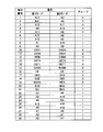
- FIG. 9 is a diagram illustrating an arrangement pattern of the external terminals TA in the first mode and the second mode.
- the first group of signals A14, BA1, A12, A6, A11, A15, A10, A1, A4 are output to the first to ninth external terminals TA, respectively, and from the 20th to 29th.
- the first group of signals BA2, BA0, A3, A9, A0, A13, A5, A7, A2, A8 are output to the second external terminal TA, respectively.
- the first group of signals A3, A6, A11, A13, A8, A0, A2, A15, A4 are output to the first to ninth external terminals TA, respectively, and from the 20th to 29th.
- the first group of signals BA2, BA1, A9, A14, BA0, A10, A12, A5, A1, A7 are output to the second external terminal TA, respectively.
- the signals A0 to A15 and BA0 to BA2 of the first group are output to the external terminals TA of Nos. 1 to 9 and 20 to 29, and whether the mode is the first mode or the second mode are 1 to 9 , 20 to 29, the order of the signals A0 to A15 and BA0 to BA2 output to the external terminals TA is changed. In other words, the order (arrangement pattern) of the external terminals TA to which the signals A0 to A15 and BA0 to BA2 are output is changed depending on whether the mode is the first mode or the second mode.
- the second group of signals CSN1, CSN0, WEN, CASN, and RASN are output to the 10th to 12th, 15th, and 19th external terminals TA, respectively.
- the second group of signals CASN, CSN1, CSN0, RASN, and WEN are output to the 10th to 12th, 15th, and 19th external terminals TA, respectively.
- the second group of signals CSN1, CSN0, WEN, CASN, and RASN are output to the 10th to 12th, 15th, and 19th external terminals TA, and whether the first mode or the second mode is 10
- the order of the signals CSN1, CSN0, WEN, CASN, and RASN output to the external terminals TA of No. 12, 15, and 19 is changed. In other words, the order (arrangement pattern) of the external terminals TA to which the signals CSN1, CSN0, WEN, CASN, and RASN are output is changed depending on whether the mode is the first mode or the second mode.
- the third group of signals ODT0, ODT1, and CKE are output to the 13th, 14th, and 18th external terminals TA, respectively.
- the switching circuit 19 can change the order of the signals ODT0, ODT1, and CKE of the third group.
- the fourth group of clock signals CK and CKN are output to the 16th and 17th external terminals TA, respectively.
- the clock signals CK and CKN are complementary signals generated based on the signal from the clock generation unit 21, and serve as a differential clock that determines a reference timing for operating the DDR2-SDRAM and the DDR3-SDRAM. Therefore, the clock signals CK and CKN are set to a fourth group different from the signals of the first to third groups, and the order of the clock signals CK and CKN by the selector 15 is not changed.
- FIGS. 10A to 10G are time charts illustrating level changes of the 16, 17, 1, 10, and 13th external terminals TA16, TA17, TA1, TA10, and TA13 in the first mode and the second mode. is there.
- the external terminals TA16, TA1, and TA10 are all fixed at “H” level, and the external terminals TA17 and TA13 are fixed at “L” level.
- clock signals CK and CKN are output to the external terminals TA16 and TA17, respectively.
- the signals A14, CSN1, and ODT0 are output to the external terminals TA1, TA10, and TA13, respectively, in synchronization with the clock signals CK and CKN.
- the semiconductor memory device 3 latches the signals A14, CSN1, and ODT0 in synchronization with the rising edge of the clock signal CK.
- the signals A3, CASN, and ODT0 are output to the external terminals TA1, TA10, and TA11 in synchronization with the clock signals CK and CKN, respectively.
- the semiconductor memory device 6 latches the signals A3, CASN, and ODT0 in synchronization with the rising edge of the clock signal CK.
- FIG. 11 is a flowchart showing the operation of the semiconductor device 1.
- a power-on reset is started in step ST1.
- the reset signal RE is set to the “H” level of the activation level
- the buffer circuits B1 to B4 are reset. That is, the output signals of the buffer circuits B1 and B2 are fixed to “H” level, the output signal of the buffer circuit B3 is fixed to “L” level, and the output signals CK and CKN of the buffer circuit B4 are respectively set to “H” level and Fixed to “L” level.
- the power-on reset is completed in step ST3.
- step ST4 the mode setting circuit 14a determines whether the semiconductor device 1 is set to the first mode or the second mode.
- the mode setting circuit 14a When determining that the semiconductor device 1 is set to the first mode, the mode setting circuit 14a generates a selector control signal SE for setting the selector 15 to the first mode and stores the selector control signal SE in the register 16 in step ST5.
- selector control signal SE for the first mode is stored in register 16, an array pattern for DDR3-SDRAM is formed by switching circuits 17-19.
- the memory controller 14 performs initialization processing for the DDR3-SDRAM in step ST6, and then starts normal access to the DDR3-SDRAM in step ST9.
- the mode setting circuit 14a If it is determined in step ST4 that the semiconductor device 1 is set to the second mode, the mode setting circuit 14a generates a selector control signal SE for setting the selector 15 in the second mode and stores it in the register 16 in step ST7. Store.
- selector control signal SE for the second mode is stored in register 16, an array pattern for DDR2-SDRAM is formed by switching circuits 17-19.
- the memory controller 14 performs initialization processing for DDR2-SDRAM in step ST8, and then starts normal access to DDR2-SDRAM in step ST9.
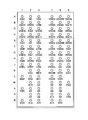
- FIG. 12 is a diagram showing an arrangement pattern of the external terminals TA of the semiconductor device 1 in the first mode.
- the semiconductor device 1 includes a plurality of external terminals TA arranged in 5 rows (A to E rows) and 25 columns.
- the external terminal TA related to the present invention will be described.
- the signals A14, BA1, A12 of the first group G1 are output to the external terminals TA of the ninth to BDth rows, respectively.
- the signals A6, A11, A15, and A10 of the first group G1 are output to the external terminals TA in the 10th column A to D rows, respectively.
- the signals A1, A4 of the first group G1 and the signal CSN1 of the second group G2 are output to the external terminals TA of the A, B, D rows in the eleventh column, respectively.
- the signals CSN0 and WEN of the second group G2 and the signals ODT0 and ODT1 of the third group G3 are output to the external terminals TA in the A to D rows of the twelfth column, respectively.
- the signal CASN of the second group G2 and the signals CK and CKN of the fourth group are output to the external terminals TA of the A, C, and D rows in the 13th column, respectively.
- the signal CKE of the third group G3, the signal RASN of the second group G2, and the signals BA2 and BA0 of the first group G1 are output to the external terminals TA in the 14th column A to D rows, respectively.
- the signals A3, A9, A0 of the first group G1 are output to the external terminals TA of the 15th column A, B, D rows, respectively.
- the signals A13, A5, A7, A2 of the first group G1 are output to the external terminals TA of the 16th column A to D rows, respectively.
- the signal A8 and the reset signal RESETN of the first group G1 are output to the external terminals TA in the 17th column B and C rows, respectively.
- VSS and VSSQ are ground voltages
- VCCQ is a power supply voltage
- VREF is a reference voltage.
- FIG. 13 is a diagram showing an arrangement pattern of the external terminals TB of the semiconductor memory device 3 (DDR3-SDRAM).
- the semiconductor memory device 3 includes a plurality of external terminals TB arranged in 16 rows (A to H, J to N, P, R, and T rows) and 6 columns (1 to 3, 7 to 9 columns). including.
- the external terminal TB related to the present invention will be described.
- FIG. 13 shows a case where the number of data inputs / outputs is 16 (DQU 0 to 7, DQL 0 to 7).
- the number of data input / output is 8 or less, there are no 3 rows A row to C row, 13 rows (D to H, J to N, P, R, T rows), 6 columns (1 to 3, 7 to 9 columns) (patterned with a dotted line in FIG. 13).
- the external terminals TB of T rows 3 columns, T rows 7 columns, and M rows 7 columns may all be set to NC (No connection). However, when the number of data inputs / outputs is 8 or less, those external terminals TB are used for inputting address signals A13 to A15, respectively.
- FIG. 13 shows a case where external terminals TB of T rows 3 columns, T rows 7 columns, and M rows 7 columns are used for input of signals A13 to A15.
- the external terminal TB in the Kth row in the first column receives the signal ODT.
- the external terminals TB in the second to Lth, N, P, R, and T rows receive signals CSN, BA0, A3, A5, A7, and RESETN, respectively.
- J to N, P, R, and T in the third column receive signals RASN, CASN, WEN, BA2, A0, A2, A9, and A13, respectively.
- the external terminals TB of J to L, N, P, R, and T rows in the seventh column receive signals CK, CKN, A10, A15, A12, A1, A11, and A14, respectively.
- the external terminals TB in the N, P, R, and T rows in the eighth column receive signals BA1, A4, A6, and A8, respectively.
- the external terminal TB in the ninth row, K row receives the signal CKE.
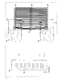
- FIGS. 14 to 16 are diagrams showing the first, third, and sixth layers of the mother board 4, respectively.
- the first layer is the surface of the mother board 4, a third layer is provided below the first layer, and a sixth layer is provided below the third layer.
- the short side and long side of the rectangular area 1A are directed to the X direction and the Y direction in FIG. 14, respectively.
- the short side and the long side of each of the rectangular regions 3A and 3B are directed to the Y direction and the X direction, respectively.
- the rectangular area 1A is arranged on the left side in FIG. 14, the rectangular area 3A is arranged on the upper right side in FIG. 14, and the rectangular area 3B is arranged on the lower right side in FIG.
- the rectangular areas 1A, 3A, and 3B are arranged with a predetermined gap therebetween.
- the rectangular area 1A is provided with a plurality of electrodes 41 corresponding to the external terminals TA of 5 rows (A to E rows) and 25 columns. Each electrode 41 is soldered to a corresponding external terminal TA of the semiconductor device 1 mounted in the rectangular area 1A. A plurality of electrodes 42 are distributed in the rectangular area 1A. Each electrode 42 is connected to the adjacent electrode 41 by wiring.
- the rectangular area 3A is provided with a plurality of electrodes 43 corresponding to external terminals TB of 16 rows (A to H, J to N, P, R, T rows) and 7 columns (1 to 3, 7 to 9 columns). It has been.
- Each electrode 43 is soldered to a corresponding external terminal TB of the semiconductor memory device 3 mounted in the rectangular area 3A.
- a plurality of electrodes 44 are distributed in the rectangular area 3A. Each electrode 44 is connected to the adjacent electrode 43 by wiring.
- 28 electrodes 45 are arranged in a staggered pattern in the X direction so as to cross the short side opposite to the rectangular region 1A of the two short sides of the rectangular region 3A.
- the fourteen electrodes 45 in the lower row in FIG. 14 and the fourteen electrodes 43 in the first to third rows of the rectangular area 3A are connected by 14 wires.
- the 14 electrodes 45 are connected to electrodes 43 for signals A7, RESETN, A5, A13, A9, A3, A2, A0, BA0, BA2, WEN, ODT, CASN, and RASN from the right side in FIG. .
- the 14 electrodes 45 in the upper row in FIG. 14 and the 14 electrodes 43 in the 2nd to 7th rows in the rectangular area 3A are connected by 14 wires.
- the 14 electrodes 45 are connected to the electrodes 43 for signals A8, A14, A6, A11, A1, A4, A12, BA1, CSN, A15, A10, CKE, CKN, and CK from the right side in FIG. .
- the rectangular region 3B is provided with a plurality of electrodes 46 corresponding to the external terminals TB of 16 rows (A to H, J to N, P, R, and T rows) and 7 columns (1 to 3, 7 to 9 columns). It has been.
- Each electrode 46 is soldered to a corresponding external terminal TB of the semiconductor memory device 3 mounted in the rectangular area 3B.
- a plurality of electrodes 47 are distributed in the rectangular area 3B. Each electrode 47 is connected to the adjacent electrode 46 by wiring.
- 28 electrodes 48 are arranged in a staggered pattern in the X direction so as to cross the short side opposite to the rectangular region 1A of the two short sides of the rectangular region 3B.
- the 14 electrodes 48 in the lower row in FIG. 14 and the 14 electrodes 46 in the 1st to 3rd rows in the rectangular area 3B are connected by 14 wires.
- the 14 electrodes 48 are connected to the electrodes 46 for signals A7, RESETN, A5, A13, A9, A3, A2, A0, BA0, BA2, WEN, ODT, CASN, and RASN from the right side in FIG. .
- the 14 electrodes 48 in the upper row in FIG. 14 and the 14 electrodes 46 in the 2nd to 7th rows in the rectangular area 3A are connected by 14 wires.
- the 14 electrodes 48 are connected to the electrodes 46 for signals A8, A14, A6, A11, A1, A4, A12, BA1, CSN, A15, A10, CKE, CKN, and CK from the right side in FIG. .
- 28 electrodes 49 are arranged at an intermediate position between the 28 electrodes 45 and the 28 electrodes 48.
- the 28 electrodes 49 are arranged in a staggered pattern in the X direction, like the electrodes 45 and 48.
- seven electrodes 49 out of the fourteen electrodes 49 in the lower column and the seven electrodes 41 in the A row and the B row of the rectangular region 1A are connected by seven wires.
- Seven electrodes 49 of Nos. 3 to 6, 11, 13, and 14 from the right side in FIG. 14 are connected to electrodes 41 for signals A5, A13, A9, A3, WEN, CASN, and RASN, respectively.
- FIG. 14 eight electrodes 49 among the fourteen electrodes 49 in the upper column and the eight electrodes 41 in the A row and the B row in the rectangular area 1A are connected by eight wires.
- the eight electrodes 49 of Nos. 1 to 6, 9, and 12 from the right side in FIG. 14 are electrodes 41 for signals A8, A14, A6, A11, A1, A4, CSN0, and CKE from the right side in FIG. Connected.
- the first group signal wiring is shown by a solid line
- the second group signal wiring is shown by a one-dot chain line
- the third group signal wiring is shown. This wiring is indicated by a dotted line.
- the third layer of the mother board 4 is provided with rectangular regions 1B, 3C, and 3D facing the rectangular regions 1A, 3A, and 3B of the first layer, respectively.
- an electrode 52 is provided to face each electrode 42 of the first layer, and each electrode 52 is connected to the corresponding electrode 42 through a via hole.
- electrodes 54 are provided to face the respective electrodes 44 of the first layer, and each electrode 54 is connected to the corresponding electrode 44 through a via hole. Further, an electrode 55 is provided to face each electrode 45 of the first layer, and each electrode 55 is connected to a corresponding electrode 45 through a via hole.
- electrodes 57 are provided to face the respective electrodes 47 of the first layer, and each electrode 57 is connected to the corresponding electrode 47 through a via hole.
- electrodes 58 are provided to face the respective electrodes 48 of the first layer, and each electrode 58 is connected to the corresponding electrode 48 through a via hole.
- an electrode 59 is provided to face each electrode 49 of the first layer, and each electrode 59 is connected to the corresponding electrode 49 through a via hole.
- each electrode 59 is connected to an electrode 55 adjacent in the Y direction by wiring, and is connected to an electrode 58 adjacent in the Y direction by wiring.
- the electrode 41 for signal A8 in B row and 17 column in FIG. 14 is connected to an electrode 49 through a wiring, and the electrode 49 is connected to an electrode 59 in FIG. 15 through a via hole.
- the electrode 59 is connected to an electrode 55 through a wiring, the electrode 55 is connected to an electrode 45 in FIG. 14 through a via hole, and the electrode 45 is connected to an electrode 43 for signal A8 in T row and 8 column.
- the address signal A8 output from the B row and 17 column external terminal TA of the semiconductor device 1 is transmitted to the T row and 8 column external terminal TB of the semiconductor memory device 3.
- the sixth layer of the mother board 4 is provided with rectangular regions 1C, 3E, 3F facing the rectangular regions 1B, 3C, 3D of the third layer, respectively.
- electrodes 62 are provided to face the respective electrodes 52 of the third layer, and each electrode 62 is connected to the corresponding electrode 52 through a via hole.
- electrodes 64 are provided to face the respective electrodes 54 of the third layer, and each electrode 64 is connected to the corresponding electrode 54 through a via hole. Further, an electrode 65 is provided to face each electrode 55 of the third layer, and each electrode 65 is connected to the corresponding electrode 55 through a via hole.
- an electrode 67 is provided to face each electrode 57 of the third layer, and each electrode 67 is connected to the corresponding electrode 57 through a via hole.
- an electrode 68 is provided to face each electrode 58 of the third layer, and each electrode 68 is connected to a corresponding electrode 58 through a via hole.
- an electrode 69 is provided to face each electrode 59 of the third layer, and each electrode 69 is connected to the corresponding electrode 59 through a via hole.
- seven electrodes 69 of the fourteen electrodes 69 in the lower row and the seven electrodes 62 in the rectangular region 1C are connected by seven wires.
- the seven electrodes 69 of Nos. 1, 2, 7 to 10, and 12 from the right side in FIG. 16 are connected to electrodes 62 for signals A7, RESETN, A2, A0, BA0, BA2, and ODT0, respectively.
- FIG. 16 six electrodes 69 out of the fourteen electrodes 69 in the upper row and the six electrodes 62 in the rectangular region 1C are connected by six wires.
- Six electrodes 69 of Nos. 7, 8, 10, 11, 13, and 14 from the right side in FIG. 16 are respectively connected to electrodes 62 for signals A12, BA1, A15, A10, CKN, and CK from the right side in FIG. Connected.
- the electrode 41 for signal A12 in D row and 9 column in FIG. 14 is connected to the adjacent electrode 42 through the wiring, and the electrode 42 is connected to the electrode 62 in FIG. 16 through the via hole, the electrode 52, and the via hole.
- the electrode 62 is connected to the electrode 69 through a wiring, and the electrode 69 is connected to the electrode 59 in FIG. 15 through a via hole.
- the electrode 59 is connected to an electrode 55 through a wiring
- the electrode 55 is connected to an electrode 45 in FIG. 14 through a via hole
- the electrode 45 is connected to an electrode 43 for signal A12 in N rows and 7 columns. .
- the address signal A12 output from the external terminal TA of D row and 9 columns of the semiconductor device 1 is transmitted to the external terminal TB of N rows and 7 columns of the semiconductor memory device 3.
- FIG. 17 is a diagram showing an arrangement pattern of the external terminals TA of the semiconductor device 1 in the second mode.
- the semiconductor device 1 includes a plurality of external terminals TA arranged in 5 rows (A to E rows) and 25 columns.
- the external terminal TA related to the present invention will be described.
- the signals A3, A6 and A11 of the first group G1 are output to the external terminals TA in the B to D rows of the ninth column, respectively.
- the signals A13, A8, A0, A2 of the first group G1 are output to the external terminals TA in the 10th column A to D rows, respectively.
- the signals A15 and A4 of the first group G1 and the signal CASN of the second group G2 are output to the external terminals TA of the A, B, and D rows in the eleventh column, respectively.
- the signals CSN1 and CSN0 of the second group G2 and the signals ODT0 and ODT1 of the third group G3 are output to the external terminals TA of the A to D rows of the twelfth column, respectively.
- the signal RASN of the second group G2 and the signals CK and CKN of the fourth group are output to the external terminals TA of the A, C, and D rows in the 13th column, respectively.
- the signal CKE of the third group G3, the signal WEN of the second group G2, and the signals BA2 and BA1 of the first group G1 are output to the external terminals TA in the A to D rows of the 14th column, respectively.
- the signals A9, A14, BA0 of the first group G1 are output to the external terminals TA of the 15th column A, B, D rows, respectively.
- the signals A10, A12, A5, A1 of the first group G1 are output to the external terminals TA of the 16th column A to D rows, respectively.
- the signal A7 of the first group G1 is output to the external terminal TA in the Bth row of the 17th column.
- VSS and VSSQ are ground voltages
- VCCQ is a power supply voltage
- VREF is a reference voltage.
- FIG. 18 is a diagram showing an arrangement pattern of the external terminals TC of the semiconductor memory device 6 (DDR2-SDRAM).
- the semiconductor memory device 6 includes a plurality of external terminals TC arranged in 15 rows (AH, JN, P, R rows) and 6 columns (1-3, 7-9 columns). .
- AH, JN, P, R rows 15 rows
- 6 columns 6 columns
- FIG. 18 shows the case where the number of data inputs / outputs is 16 (DQ0 to 15).
- the number of data input / output is 8 or less, there are no 4 rows A row to D row, 11 rows (E to H, J to N, P, R rows), 6 columns (1 to 3, 7 to 9 columns) ) (An area surrounded by a dotted line in FIG. 18).
- the external terminals TC of R rows 3, 7, and 8 columns may both be NC. However, when the number of data inputs / outputs is 8 or less, these external terminals TC are used for inputting address signals A14, A15, A13, respectively.
- FIG. 18 shows a case where the external terminals TC of the third, seventh, and eighth columns in the R row are used for inputting signals A14, A15, and A13.
- the external terminal TC in the L row of the first column receives the signal BA2.
- the external terminals TC of the second column K to N, P, and R rows receive signals CKE, BA0, A10, A3, A7, and A12, respectively.
- the external terminals TC of K to N, P, and R in the third column receive signals WEN, BA1, A1, A5, A9, and A14, respectively.
- the external terminals TC in the Kth to Nth, Pth, and Rth rows in the seventh column receive signals RASN, CASN, A2, A6, A11, and A15, respectively.
- the external terminals TC of the eighth to Jth rows, Nth, Pth and Rth rows receive the signals CK, CKN, A0, A4, A8 and A13, respectively.
- the external terminal TC in the Kth row in the ninth column receives the signal ODT.
- 19 to 21 are diagrams showing the first, third, and sixth layers of the mother board 7, respectively.
- the first layer is the surface of the mother board 7, the third layer is provided below the first layer, and the sixth layer is provided below the third layer.
- the short side and the long side of the rectangular area 1A are directed in the X direction and the Y direction in FIG. 19, respectively.
- the short side and the long side of each of the rectangular regions 6A and 6B are directed to the Y direction and the X direction, respectively.
- the rectangular area 1A is arranged on the left side in FIG. 19, the rectangular area 6A is arranged on the upper right side in FIG. 19, and the rectangular area 6B is arranged on the lower right side in FIG.
- the rectangular areas 1A, 6A, and 6B are arranged with a predetermined gap therebetween.
- a plurality of electrodes 71 corresponding to the external terminals TA of 5 rows (A to E rows) and 25 columns are provided. Each electrode 71 is soldered to a corresponding external terminal TA of the semiconductor device 1 mounted in the rectangular area 1A.
- a plurality of electrodes 72 are distributed in the rectangular area 1A. Each electrode 72 is connected to the adjacent electrode 71 by wiring.
- the rectangular area 6A is provided with a plurality of electrodes 73 corresponding to the external terminals TB of 15 rows (A to H, J to N, P, and R rows) and 7 columns (1 to 3, 7 to 9 columns). Yes.
- Each electrode 73 is soldered to a corresponding external terminal TC of the semiconductor memory device 6 mounted in the rectangular area 6A.
- a plurality of electrodes 74 are dispersedly arranged in the rectangular area 6A. Each electrode 74 is connected to the adjacent electrode 73 by wiring.
- 25 electrodes 75 are arranged in a staggered pattern in the X direction so as to cross the short side opposite to the rectangular region 1A of the two short sides of the rectangular region 6A.
- the 13 electrodes 75 in the lower row in FIG. 19 and the 13 electrodes 73 in the first to third rows of the rectangular area 6A are connected by 13 wires.
- Thirteen electrodes 75 are connected to electrodes 73 for signals A3, A7, A12, A10, A14, A9, A5, A1, BA0, BA1, BA2, WEN, and CKE from the right side in FIG.
- the 12 electrodes 75 in the upper row and the 12 electrodes 73 in the 7th to 9th rows in the rectangular area 6A are connected by 12 wires.
- the twelve electrodes 75 are respectively connected to the electrodes 73 for signals A8, A13, A2, A15, A11, A6, A0, A2, CSN0, CASN, ODT0, and RASN from the right side in FIG.
- the rectangular area 6B is provided with a plurality of electrodes 76 corresponding to the external terminals TB of 15 rows (A to H, J to N, P, and R rows) and 7 columns (1 to 3, 7 to 9 columns). Yes.
- Each electrode 76 is soldered to a corresponding external terminal TC of the semiconductor memory device 6 mounted in the rectangular area 6B.
- a plurality of electrodes 77 are distributed in the rectangular area 6B. Each electrode 77 is connected to an adjacent electrode 76 by wiring.
- 25 electrodes 78 are arranged in a staggered pattern in the X direction so as to cross the short side opposite to the rectangular region 1A of the two short sides of the rectangular region 6B.
- the 13 electrodes 78 in the lower row in FIG. 19 and the 13 electrodes 76 in the 1st to 3rd rows in the rectangular area 6B are connected by 13 wires.
- Thirteen electrodes 78 are connected to electrodes 76 for signals A3, A7, A12, A10, A14, A9, A5, A1, BA0, BA1, BA2, WEN, and CKE from the right side in FIG.
- the 12 electrodes 78 in the upper row and the 12 electrodes 76 in the 7th to 9th rows in the rectangular area 6A are connected by 12 wires.
- the twelve electrodes 78 are connected to electrodes 76 for signals A8, A13, A2, A15, A11, A6, A0, A2, CSN0, CASN, ODT0, and RASN from the right side in FIG.
- 25 electrodes 79 are arranged at an intermediate position between the 25 electrodes 75 and the 25 electrodes 78.
- the 25 electrodes 79 are arranged in a staggered pattern in the X direction, like the electrodes 75 and 78.
- seven of the thirteen electrodes 79 in the lower column and the seven electrodes 71 in the A and B rows of the rectangular region 1A are connected by seven wires.
- the seven electrodes 79 of Nos. 1 to 6, 12, and 13 from the right side in FIG. 19 are connected to electrodes 71 for signals A3, A7, A12, A10, A14, A9, WEN, and CKE, respectively.
- FIG. 19 six electrodes 79 out of twelve electrodes 79 in the upper column and six electrodes 71 in the A and B rows of the rectangular area 1A are connected by six wires.
- the six electrodes 79 1 to 4, 9, and 12 from the right side in FIG. 19 are connected to the electrodes 71 for signals A8, A13, A2, A15, CSN0, and RASN from the right side in FIG.
- the first group of signal wires among the wires between the electrodes 71 and 79 are indicated by solid lines
- the second group signal wires are indicated by one-dot chain lines
- the third group signal wires are indicated. This wiring is indicated by a dotted line.
- the third layer of the mother board 7 is provided with rectangular regions 1B, 6C, and 6D facing the rectangular regions 1A, 6A, and 6B of the first layer, respectively.
- an electrode 82 is provided to face each electrode 72 of the first layer, and each electrode 82 is connected to the corresponding electrode 72 through a via hole.
- electrodes 84 are provided to face the respective electrodes 74 of the first layer, and each electrode 84 is connected to the corresponding electrode 74 through a via hole.
- an electrode 85 is provided to face each electrode 75 of the first layer, and each electrode 85 is connected to a corresponding electrode 75 through a via hole.
- electrodes 87 are provided to face the respective electrodes 77 of the first layer, and each electrode 87 is connected to the corresponding electrode 77 through a via hole.
- an electrode 88 is provided to face each electrode 78 of the first layer, and each electrode 88 is connected to the corresponding electrode 78 through a via hole.
- an electrode 89 is provided to face each electrode 79 of the first layer, and each electrode 89 is connected to the corresponding electrode 79 through a via hole.
- each electrode 89 is connected to an electrode 85 adjacent in the Y direction by wiring, and is connected to an electrode 88 adjacent in the Y direction by wiring.
- two electrodes 83 are provided at an intermediate position between the rectangular regions 6C and 6D. Each electrode 83 is connected to corresponding electrodes 84 and 87 by wiring extending in the Y direction.
- the electrode 71 for signal A7 in B row and 17 column in FIG. 19 is connected to an electrode 79 through a wiring, and the electrode 79 is connected to an electrode 89 in FIG. 20 through a via hole.
- the electrode 89 is connected to an electrode 85 through a wiring
- the electrode 85 is connected to an electrode 75 in FIG. 19 through a via hole
- the electrode 75 is connected to an electrode 73 for signal A7 in N rows and 2 columns. .
- the address signal A7 output from the external terminal TA of the B row and 17 column of the semiconductor device 1 is transmitted to the external terminal TC of the N row and 2 column of the semiconductor memory device 6.
- the sixth layer of the mother board 7 is provided with rectangular regions 1C, 6E, and 6F facing the rectangular regions 1B, 6C, and 6D of the third layer, respectively.
- an electrode 92 is provided to face each electrode 82 of the third layer, and each electrode 92 is connected to the corresponding electrode 82 through a via hole.
- electrodes 94 are provided to face the respective electrodes 84 of the third layer, and each electrode 94 is connected to the corresponding electrode 84 through a via hole. Further, an electrode 95 is provided to face each electrode 85 of the third layer, and each electrode 95 is connected to the corresponding electrode 85 through a via hole.
- electrodes 97 are provided so as to face the respective electrodes 87 of the third layer, and each electrode 97 is connected to the corresponding electrode 87 through a via hole.
- an electrode 98 is provided to face each electrode 88 of the third layer, and each electrode 98 is connected to the corresponding electrode 88 through a via hole.
- an electrode 99 is provided to face each electrode 89 of the third layer, and each electrode 99 is connected to a corresponding electrode 89 through a via hole.
- the five electrodes 99 of the 13 electrodes 99 in the lower row in FIG. 21 and the five electrodes 92 in the rectangular region 1C are connected by five wires.
- the five electrodes 99 from No. 7 to 11 from the right side in FIG. 21 are connected to electrodes 92 for signals A5, A1, BA0, BA1, and BA2, respectively.
- an electrode 93 is provided to face each electrode 83 of the third layer, and each electrode 93 is connected to the corresponding electrode 83 through a via hole.
- the two electrodes 93 in FIG. 21 are connected to the electrodes 92 for signals CKN and CK from the right side in FIG.
- the electrode 71 for signal A11 in D row and 9 column in FIG. 19 is connected to an adjacent electrode 92 through a wiring, and the electrode 92 is connected to the electrode 92 in FIG. 21 through a via hole, an electrode 82, and a via hole.
- the electrode 92 is connected to the electrode 99 through a wiring, and the electrode 99 is connected to the electrode 89 in FIG. 20 through a via hole.
- the electrode 89 is connected to an electrode 85 through a wiring
- the electrode 85 is connected to an electrode 75 in FIG. 19 through a via hole
- the electrode 75 is connected to an electrode 73 for signal A11 in P row and 7 column.
- the address signal A11 output from the external terminal TA of the D row and the 9th column of the semiconductor device 1 is transmitted to the external terminal TB of the P row and the 7th column of the semiconductor memory device 6.
- FIGS. 22B and 22C are diagrams showing semiconductor modules 102 and 105, respectively.
- a semiconductor device 101 is obtained by mounting a semiconductor chip on the surface of a package substrate and sealing it with a resin, and a plurality of external terminals TD are arranged in a matrix on the back surface of the package substrate.
- the semiconductor chip has a memory controller or the like formed on the surface of a semiconductor substrate, and is connected to a plurality of external terminals TD via a package substrate.
- the semiconductor module 102 is obtained by mounting the semiconductor device 101 and one semiconductor memory device 3 on the surface of one motherboard 103.
- Semiconductor memory device 3 is, for example, a DDR3-SDRAM.
- the semiconductor memory device 3 has semiconductor memory chips mounted on the front surface of a package substrate and sealed with resin, and a plurality of external terminals TB are arranged in a matrix on the back surface of the package substrate.
- the semiconductor memory chip has a plurality of memory cells, write / read circuits, etc. formed on the surface of a semiconductor substrate, and is connected to a plurality of external terminals TB via a package substrate.
- the plurality of external terminals TB of the semiconductor memory device 3 are arranged according to a predetermined arrangement pattern.
- the arrangement pattern of the external terminals TB of the semiconductor memory device 3 is fixed. That is, the type of signal input to each external terminal TB is fixed.
- the arrangement pattern of the external terminals TB of the semiconductor device 101 is changed according to the number of semiconductor memory devices 3 by a built-in switching circuit. That is, the type of signal output from each external terminal TB can be changed by the switching circuit.
- the configuration of the semiconductor device 101 is the same as the configuration of the semiconductor device 1.
- a plurality of wirings for connecting the plurality of external terminals TD of the semiconductor device 101 and the plurality of external terminals TB of the semiconductor memory device 3 are formed on the mother board 103.
- the arrangement pattern of the external terminals TD of the semiconductor device 101 is set so that the wirings of the mother board 103 do not intersect on the same layer.
- Each external terminal TB of the semiconductor memory device 3 is connected to a corresponding external terminal TD of the semiconductor device 101 via the wiring of the mother board 103.
- the semiconductor module 105 is obtained by mounting the semiconductor device 101 and the four semiconductor memory devices 3 on the surface of one motherboard 106.
- the arrangement patterns of the external terminals TB of the four semiconductor memory devices 3 are the same, but when one semiconductor memory device 3 is connected to the semiconductor device 101 and when four semiconductor memory devices 3 are connected to the semiconductor device 101. Then, the wiring arrangement is different.
- the arrangement pattern of the external terminals TD of the semiconductor device 101 is changed according to the number of semiconductor memory devices 3 by a built-in switching circuit.
- a plurality of wirings for connecting the plurality of external terminals TD of the semiconductor device 101 and the plurality of external terminals TB of the four semiconductor memory devices 3 are formed on the mother board 106.
- the arrangement pattern of the external terminals TD of the semiconductor device 101 is set so that the wirings of the mother board 106 do not intersect on the same layer.
- Each external terminal TB of each semiconductor memory device 3 is connected to a corresponding external terminal TD of the semiconductor device 101 via the wiring of the mother board 106.
- the cost of the semiconductor device 101 can be reduced.
- FIG. 23A is a view of the semiconductor device 101 and one semiconductor memory device 3 as seen from the back side.
- a plurality of external terminals TD are arranged in a matrix on the rectangular back surface of the semiconductor device 101.
- a plurality of external terminals TB are arranged in a matrix on the rectangular back surface of each semiconductor memory device 3.
- One side of the semiconductor device 101 and one side of the semiconductor memory device 3 are arranged to face each other.
- eight external terminals TB for signals RAS, A1, A2, CAS, CS, A5, CK, and CKN are provided along the three sides of the semiconductor memory device 3, respectively.
- eight external terminals TD for signals RAS, A1, A2, CAS, CS, A5, CK, and CKN are provided along one side of the semiconductor device 101 opposite to one side of the semiconductor memory device 3.
- the eight external terminals TD of the semiconductor device 101 and the total eight external terminals TB of one semiconductor memory device 3 can be connected by eight wirings LB that do not intersect.
- FIG. 23B is a view of the semiconductor device 101 and the two semiconductor memory devices 3 as seen from the back side.
- a plurality of external terminals TD are arranged in a matrix on the rectangular back surface of the semiconductor device 101.
- a plurality of external terminals TB are arranged in a matrix on the rectangular back surface of each semiconductor memory device 3.
- One side of the semiconductor device 1 and one side of the two semiconductor memory devices 3 are arranged to face each other.
- each semiconductor memory device 3 It is assumed that eight external terminals TB for signals RAS, A1, A2, CAS, CS, A5, CK, and CKN are provided along the three sides of each semiconductor memory device 3, respectively.
- the arrangement pattern shown in FIG. 22A is adopted as the arrangement pattern of the external terminals TD of the semiconductor device 101, and each external terminal TD of the semiconductor device 101 is connected to the corresponding external terminal TB via the wiring LB.
- the wirings LB intersect at many places.
- nine wirings LB crossing between the semiconductor device 101 and the semiconductor memory device 3 are arranged. Therefore, cost increases, transmission characteristics deteriorate, and the substrate area increases.
- the external terminal of the semiconductor device 101 is connected by a built-in switching circuit. Since the TD array pattern is changed in accordance with the external terminals TB of the two semiconductor memory devices 3, the number of times the wiring lines LB intersect each other can be reduced. In addition, the number of wirings LB between the semiconductor device 101 and the semiconductor memory device 3 can be reduced. For example, in FIG. 22B, nine wirings LB are provided between the semiconductor device 101 and the semiconductor memory device 3, whereas in FIG. 22C, between the semiconductor device 101 and the semiconductor memory device 3. Six wirings LB are provided.
- the semiconductor device 101 when the semiconductor module 102 is configured by the semiconductor device 101 and one semiconductor memory device 3, the semiconductor device 101 is set to the first mode by the mode setting signal.
- the semiconductor device 101 set to the first mode outputs signals RAS, A1, A2, CAS, CS, A5, CK, and CKN from eight external terminals TD facing one side of one semiconductor memory device 3, respectively. To do. Therefore, the eight wirings LB can be formed on the mother board 103 without crossing.
- the semiconductor device 101 is set to the second mode by the mode setting signal.
- the semiconductor device 1 set to the second mode outputs signals CS, CAS, A5, RAS, A2, A1, CK, and CKN from eight external terminals TD facing one side of the two semiconductor memory devices 3, respectively. To do. In this case, the number of intersections between the wirings LB on the mother board 106 can be reduced, and the number of wirings LB crossing between the semiconductor device 101 and the semiconductor memory device 3 can be reduced. Also in this second embodiment, the same effect as in the first embodiment can be obtained.
Landscapes
- Engineering & Computer Science (AREA)
- Theoretical Computer Science (AREA)
- Physics & Mathematics (AREA)
- General Engineering & Computer Science (AREA)
- General Physics & Mathematics (AREA)
- Dram (AREA)
- Semiconductor Integrated Circuits (AREA)
- Design And Manufacture Of Integrated Circuits (AREA)
Abstract
半導体装置(1)は、3つのグループに分割された複数の信号(S1~S3)を出力するメモリコントローラ(14)と、それぞれ3つのグループに対応して設けられた3個の切換回路(17~19)と、3つのグループに分割された複数のバッファ回路(B1~B3)と、それぞれ複数のバッファ回路(B1~B3)に対応して設けられた複数の外部端子(TA)とを備える。各切換回路は、対応のグループの複数の信号を、セレクタ制御信号(SE)に応じた順序で対応のグループの複数のバッファ回路に並列に与える。
Description
この発明は半導体装置に関し、特に、複数の配線を介して半導体メモリ装置に接続される半導体装置に関する。
DRAM(Dynamic Random Access Memory)、SRAM(Static Random Access Memory)などの半導体メモリ装置は、半導体メモリチップをパッケージ基板の表面に搭載して樹脂で封止したものであり、パッケージ基板の裏面には複数の外部端子が行列状に配置されている。半導体メモリチップは、半導体基板の表面に複数のメモリセル、書込/読出回路などを形成したものであり、パッケージ基板を介して複数の外部端子に接続される。半導体メモリ装置の外部端子の配列パターンは、半導体メモリ装置の機種毎に異なる(たとえば、特開2003-51545号公報(特許文献1)参照)。
また、このような半導体メモリ装置を制御する半導体装置は、半導体チップをパッケージ基板の表面に搭載して樹脂で封止したものであり、パッケージ基板の裏面には複数の外部端子が行列状に配置されている。半導体チップは、半導体基板の表面にメモリコントローラなどを形成したものであり、パッケージ基板を介して複数の外部端子に接続される。半導体装置の外部端子の配列パターンは、半導体メモリ装置の外部端子の配列パターンに合せて設定される。
半導体メモリ装置と半導体装置は、1枚のマザーボードに搭載されて1つの半導体モジュールを構成する。半導体メモリ装置の各外部端子は、マザーボードの配線を介して半導体装置の対応の外部端子に接続される(たとえば、特開2010-123203号公報(特許文献2)参照)。
半導体装置と1または2以上の半導体メモリ装置とを1枚のマザーボードに搭載して半導体モジュールを構成する場合、マザーボードの配線同士が交差しないように、半導体メモリ装置の機種および数に合せて半導体装置の外部端子の配列パターンを最適に設計する必要がある。しかし、半導体メモリ装置の機種や数が変わる度に半導体装置の外部端子の配列パターンを変えると、半導体装置がコスト高になるという問題がある。
それゆえに、この発明の主たる目的は、低コストの半導体装置を提供することである。
この発明に係る半導体装置は、予めM個(ただし、Mは2以上の整数である)の信号グループに分割されたN個(ただし、NはMよりも大きな整数である)の信号を出力する信号発生回路と、それぞれM個の信号グループに対応して設けられたM個の切換回路と、それぞれM個の切換回路に対応するM個のバッファグループに分割されたN個のバッファ回路と、それぞれN個のバッファ回路に対応して設けられたN個の外部端子とを備えたものである。各信号グループは複数の信号を含み、各バッファグループは対応の信号グループの信号と同数のバッファ回路を含む。各切換回路は、対応の信号グループの複数の信号を、モード設定信号に応じた順序で対応のバッファグループの複数のバッファ回路に並列に与える。各バッファグループの各バッファ回路は、対応の切換回路から与えられた信号を対応の外部端子に与える。
この発明に係る半導体装置では、切換回路は、信号発生回路で生成された複数の信号を、モード設定信号に応じた順序で複数のバッファ回路に並列に与える。したがって、接続される半導体メモリ装置の機種および数に応じて外部端子の配列パターンを切換えることができるので、装置の低コスト化を図ることができる。
[実施の形態1]
図1(a)は本発明の実施の形態1による半導体装置(LSI:Large Scale Integration)1の構成を示す図であり、図1(b)(c)はそれぞれ半導体装置1を用いた半導体モジュール2,5を示す図である。
図1(a)は本発明の実施の形態1による半導体装置(LSI:Large Scale Integration)1の構成を示す図であり、図1(b)(c)はそれぞれ半導体装置1を用いた半導体モジュール2,5を示す図である。
図1(a)において、半導体装置1は、半導体チップをパッケージ基板の表面に搭載して樹脂で封止したものであり、パッケージ基板の裏面には複数の外部端子TAが行列状に配置されている。半導体チップは、半導体基板の表面にメモリコントローラなどを形成したものであり、パッケージ基板を介して複数の外部端子TAに接続される。
また図1(b)において、半導体モジュール2は、半導体装置1と2つの半導体メモリ装置3とを1枚のマザーボード4の表面に搭載したものである。半導体メモリ装置3は、たとえばDDR3-SDRAM(Double Data Rate3-Synchronous Dynamic Random Access Memory)である。半導体メモリ装置3は、半導体メモリチップをパッケージ基板の表面に搭載して樹脂で封止したものであり、パッケージ基板の裏面には複数の外部端子TBが行列状に配置されている。半導体メモリチップは、半導体基板の表面に複数のメモリセル、書込/読出回路などを形成したものであり、パッケージ基板を介して複数の外部端子TBに接続される。
半導体メモリ装置3の複数の外部端子TBは、所定の配列パターンに従って配置されている。半導体メモリ装置3の外部端子TBの配列パターンは固定されている。つまり、各外部端子TBに入力される信号の種類は固定されている。一方、半導体装置1の外部端子TAの配列パターンは、内蔵の切換回路により、半導体メモリ装置3の外部端子TBの配列パターンに合せて設定される。つまり、各外部端子TAから出力される信号の種類は、切換回路によって変更可能になっている。切換回路については後述する。
マザーボード4には、半導体装置1の複数の外部端子TAと半導体メモリ装置3の複数の外部端子TBとを接続するための複数の配線が形成されている。半導体装置1の外部端子TAの配列パターンは、マザーボード4の配線同士が同一レイヤで交差しないように設定される。半導体メモリ装置3の各外部端子TBは、マザーボード4の配線を介して半導体装置1の対応の外部端子TAに接続される。
また図1(c)において、半導体モジュール5は、半導体装置1と2つの半導体メモリ装置6とを1枚のマザーボード7の表面に搭載したものである。半導体メモリ装置6は、半導体メモリ装置3と異なる機種の半導体メモリ装置であり、たとえばDDR2-SDRAMである。半導体メモリ装置6は、半導体メモリチップをパッケージ基板の表面に搭載して樹脂で封止したものであり、パッケージ基板の裏面には複数の外部端子TCが行列状に配置されている。半導体メモリチップは、半導体基板の表面に複数のメモリセル、書込/読出回路などを形成したものであり、パッケージ基板を介して複数の外部端子TCに接続される。
半導体メモリ装置6の複数の外部端子TCは、所定の配列パターンに従って配置されている。半導体メモリ装置6の外部端子TCの配列パターンは固定されており、半導体メモリ装置3の外部端子TBの配列パターンと異なる。一方、半導体装置1の外部端子TAの配列パターンは、内蔵の切換回路により、半導体メモリ装置6の外部端子TCの配列パターンに応じて設定される。
マザーボード7には、半導体装置1の複数の外部端子TAと半導体メモリ装置6の複数の外部端子TCとを接続するための複数の配線が形成されている。半導体装置1の外部端子TAの配列パターンは、マザーボード7の配線同士が交差しないように設定される。半導体メモリ装置6の各外部端子TCは、マザーボード7の配線を介して半導体装置1の対応の外部端子TAに接続される。
このように、本実施の形態1では、接続される半導体メモリ装置の機種に応じて半導体装置1の外部端子TAのパターン配列を変更することができるので、装置の低コスト化および信号伝送特性の改善を図ることができる。
図2(a)~(c)は、実施の形態1の効果を示す図である。図2(a)は、半導体装置1と2つの半導体メモリ装置3を裏面側から見た図である。図2(a)において、半導体装置1の四角形状の裏面には複数の外部端子TAが行列状に配置されている。また、各半導体メモリ装置3の四角形状の裏面には、複数の外部端子TBが行列状に配置されている。半導体装置1の1辺と2つの半導体メモリ装置3の1辺とは、対向して配置されている。
2つの半導体メモリ装置3のうちの一方の半導体メモリ装置3の1辺に沿って、それぞれ信号A1,A2,RAS0,CAS0用の4つの外部端子TBが設けられているものとする。また、他方の半導体メモリ装置3の1辺に沿って、それぞれ信号A5,A6,RAS1,CAS1用の4つの外部端子TBが設けられているものとする。
この場合、2つの半導体メモリ装置3の1辺に対向する半導体装置1の1辺に沿って、信号A1,A2,RAS0,CAS0,A5,A6,RAS1,CAS1用の8個の外部端子TAを設ければ、半導体装置1の8個の外部端子TAと2つの半導体メモリ装置3の合計8個の外部端子TBとを交差しない8本の配線LBで接続することができる。
また図2(b)は、半導体装置1と2つの半導体メモリ装置6を裏面側から見た図である。図2(b)において、半導体装置1の四角形状の裏面には複数の外部端子TAが行列状に配置されている。また、各半導体メモリ装置6の四角形状の裏面には、複数の外部端子TCが行列状に配置されている。半導体装置1の1辺と2つの半導体メモリ装置6の1辺とは、対向して配置されている。
2つの半導体メモリ装置6のうちの一方の半導体メモリ装置6の1辺に沿って、それぞれ信号A2,A1,RAS0,CAS0用の4つの外部端子TCが設けられているものとする。また、他方の半導体メモリ装置6の1辺に沿って、それぞれ信号A6,A5,RAS1,CAS1用の4つの外部端子TCが設けられているものとする。
この場合、半導体装置1の外部端子TAの配列パターンとして図2(a)で示した配列パターンを採用して、半導体装置1の各外部端子TAを配線LCを介して対応の外部端子TCに接続すると、図2(b)に示すように、8本の配線LCが4箇所で交差してしまう。2本の配線LCが交差すると、一方の配線LCを他方の配線LCの下方を通過させる必要が生じ、一方の配線LCの配線長が他方の配線LCより増加することにより信号間の伝送特性にずれ(スキュー)が発生し、結果として伝送特性の悪化を招くことがある。
これに対して本実施の形態1では、図2(c)に示すように、半導体装置1と半導体メモリ装置6とを接続する場合は、内蔵の切換回路により、半導体装置1の外部端子TAの配列パターンを半導体メモリ装置6の外部端子TCに合せて変更するので、配線LCの交差を解消することができる。
すなわち、本実施の形態1では、半導体装置1と2つの半導体メモリ装置3で半導体モジュール2を構成する場合は、半導体装置1はモード設定信号によって第1モードに設定される。第1モードに設定された半導体装置1は、2つの半導体メモリ装置3の1辺に対向する8個の外部端子TAからそれぞれ信号A1,A2,RAS0,CAS0,A5,A6,RAS1,CAS1を出力する。したがって、マザーボード4には、8本の配線LBを交差させることなく形成することができる。
また、半導体装置1と2つの半導体メモリ装置6で半導体モジュール5を構成する場合は、半導体装置1はモード設定信号によって第2モードに設定される。第2モードに設定された半導体装置1は、2つの半導体メモリ装置6の1辺に対向する8個の外部端子TAからそれぞれ信号A2,A1,CAS0,RAS0,A6,A5,CAS1,RAS1を出力する。したがって、マザーボード7には、8本の配線LCを交差させることなく形成することができる。
図3(a)(b)は、半導体装置1と半導体メモリ装置6を裏面側から見た図であって、実施の形態1の効果を示す他の図である。図3(a)(b)では、半導体装置1の複数の外部端子TAと半導体メモリ装置6の複数の外部端子TCとが複数の配線LCで接続されている。
図3(a)では、半導体メモリ装置6に対する半導体装置1の外部端子TAの配列パターンが適切でないために、複数の配線LCが複数箇所で交差している。2本の配線LCが交差する箇所では、2本の配線LCを同じ配線層で形成することができず、一方の配線LCを他の配線層で形成し、上層の配線LCと下層の配線LCをビアホールで接続する必要がある。したがって、配線層の数が増加するので、コスト高になる。また、信号が複数のビアホールを介して伝送されるので、伝送特性が悪化する。また、配線LCのレイアウト面積が増大する。
これに対して本願発明では、図3(b)に示すように、半導体メモリ装置6に対する半導体装置1の外部端子TAの配列パターンが適切に設定されるので、配線LC同士が交差しない。したがって、低コストで、伝送特性が良好で、レイアウト面積が小さな半導体モジュール5を構成することができる。
以下、半導体装置1および半導体モジュール2,5の構成について、より詳細に説明する。図4は、半導体装置1に含まれる半導体チップ10の構成を示すブロック図である。図4において、この半導体チップ10は、半導体基板11を備える。半導体基板11には、入力端子TI1,TI2、複数のパッドP、システムコントローラ(SYSC)12、バス13、メモリコントローラ14、セレクタ15、信号入出力回路20が形成されている。
入力端子TI1には、半導体装置1内の他の半導体チップあるいは半導体装置1外からパワーオンリセット信号PORが与えられる。パワーオンリセット信号PORは、半導体装置1に電源電圧が供給されたときに所定期間だけ活性化レベルにされる信号である。入力端子TI2には、外部からモード設定信号MODEが与えられる。たとえば、半導体装置1を第1モードに設定する場合はモード設定信号MODEは「L」レベルに設定され、半導体装置1を第2モードに設定する場合はモード設定信号MODEは「H」レベルに設定される。各パッドPは、たとえばボンディングワイヤを介してパッケージ基板に接続され、さらにパッケージ基板の配線を介して対応の外部端子TAに接続される。
システムコントローラ12は、パワーオンリセット信号PORが活性化レベルにされたときにリセットされ、バス13を介して半導体チップ10全体を制御する。メモリコントローラ14は、システムコントローラ12などからバス13を介して与えられる信号に従って、半導体メモリ装置を制御するための複数の信号Sを生成する。複数の信号Sは、予め3つの信号グループに分割されている。
第1信号グループに属する複数の信号S1の各々は、パワーオンリセット信号PORなどによって半導体チップ10がリセットされたとき、「H」レベルと「L」レベルのうちのいずれのレベルにされてもよい信号である。複数の信号S1は、具体的には、アドレス信号A00~A15およびバンクアドレス信号BA0~BA2である。
第2信号グループに属する複数の信号S2の各々は、パワーオンリセット信号PORなどによって半導体チップ10がリセットされたとき、強制的に「H」レベルにされるべき信号である。複数の信号S2は、具体的には、チップセレクト信号CSN0,CSN1、ライトイネーブル信号WEN、列アドレスストローブ信号CASN、行アドレスストローブ信号RASNである。
第3信号グループに属する複数の信号S3の各々は、パワーオンリセット信号PORなどによって半導体チップ10がリセットされたとき、強制的に「L」レベルにされるべき信号である。複数の信号S3は、具体的には、信号ODT0,ODT1およびクロックイネーブル信号CKEである。第1信号グループの複数の信号S1、第2信号グループの複数の信号S2、および第3信号グループの複数の信号S3は、セレクタ15に与えられる。
また、メモリコントローラ14に含まれるモード設定回路14aは、外部から入力端子TI2を介して与えられたモード設定信号MODEに従って、セレクタ制御信号SEを生成する。セレクタ制御信号SEは、セレクタ15に与えられる。
セレクタ15は、レジスタ16および切換回路17~19を含む。レジスタ16は、モード設定回路14aからのセレクタ制御信号SEを保持するとともに、そのセレクタ制御信号SEを切換回路17~19の各々に与える。切換回路17は、レジスタ16からのセレクタ制御信号SEに応じた順序で、メモリコントローラ14からの複数の信号S1を信号入出力回路20に並列に与える。切換回路18は、レジスタ16からのセレクタ制御信号SEに応じた順序で、メモリコントローラ14からの複数の信号S2を信号入出力回路20に並列に与える。切換回路19は、レジスタ16からのセレクタ制御信号SEに応じた順序で、メモリコントローラ14からの複数の信号S3を信号入出力回路20に並列に与える。
信号入出力回路20は、メモリコントローラ14からセレクタ15を介して与えられた複数の信号S1、複数の信号S2、および複数の信号S3をそれぞれ複数のパッドPに伝達させる。また、信号入出力回路20は、クロック信号CK,CKNを生成して2つのパッドPに与える。
すなわち、信号入出力回路20は、図5に示すように、それぞれ切換回路17からの複数の信号S1に対応して設けられた複数のバッファ回路B1と、それぞれ切換回路18からの複数の信号S2に対応して設けられた複数のバッファ回路B2と、それぞれ切換回路19からの複数の信号S3に対応して設けられた複数のバッファ回路B3と、クロック生成部21と、バッファ回路B4とを含む。
複数のパッドPは、それぞれ複数のバッファ回路B1に対応する複数のパッドP1と、それぞれ複数のバッファ回路B2に対応する複数のパッドP2と、それぞれ複数のバッファ回路B3に対応する複数のパッドP3と、バッファ回路B4に対応する2つのパッドP4A,P4Bとを含む。
各バッファ回路B1は、切換回路17からの信号S1を対応のパッドP1に伝達させる。各バッファ回路B2は、切換回路18からの信号S2を対応のパッドP2に伝達させる。各バッファ回路B3は、切換回路19からの信号S3を対応のパッドP3に伝達させる。クロック生成部21は、クロック信号CKを生成する。バッファ回路B4は、クロック生成部21からのクロック信号CKに応答してクロック信号CKの相補信号CKNを生成し、クロック信号CK,CKNをそれぞれパッドP4A,P4Bに与える。
信号S1に対応するバッファ回路B1は、図6に示すように、レベルアップシフタ(LU)22,23,25、レベルダウンシフタ(LD)24、バッファ26、およびコンパレータ27を含む。メモリコントローラ14の電源電圧はたとえば1.0Vであり、半導体メモリ装置3,6の電源電圧はたとえば1.5Vである。
レベルアップシフタ22は、メモリコントローラ14からの信号S1の論理振幅電圧を1.0Vから1.5Vに変換してバッファ26の入力ノードに与える。また、レベルアップシフタ22は、リセット信号REが活性化レベルの「H」レベルにされると、信号S1の論理レベルに関係なく「H」レベルの信号を出力する。パワーオンリセット信号PORが活性化レベルにされると、リセット信号REが活性化レベルにされる。
レベルアップシフタ23は、アウトプットイネーブル信号OENの論理振幅電圧を1.0Vから1.5Vに変換してバッファ26の制御ノードに与える。信号OENは、信号S1を外部に出力する場合は活性化レベルの「L」レベルにされ、信号S1を外部に出力しない場合は非活性化レベルの「H」レベルにされる。また、レベルアップシフタ23は、リセット信号REが活性化レベルの「H」レベルにされると、信号OENの論理レベルに関係なく「L」レベルを出力する。
バッファ26は、半導体メモリ装置3,6の電源電圧である1.5Vで駆動される。バッファ26は、レベルアップシフタ23の出力信号26OENが活性化レベルの「L」レベルにされた場合は信号S1をパッドP1に出力し、信号26OENが非活性化レベルの「H」レベルにされた場合はパッドP1をハイ・インピーダンス状態にする。したがって、リセット信号REが活性化レベルの「H」レベルにされた場合は、信号S1,OENの論理レベルに関係なく、パッドP1は「H」レベルにされる。
レベルダウンシフタ24、レベルアップシフタ25、およびコンパレータ27は、出荷前の半導体装置1をテストするときに使用されるものであり、通常は使用されないので点線で示されている。
レベルアップシフタ25は、インプットイネーブル信号IEの論理振幅電圧を1.0Vから1.5Vに変換してコンパレータ27の制御ノードに与える。信号IEは、テストモード時は活性化レベルの「H」レベルにされ、通常動作時は非活性化レベルの「L」レベルにされる。また、レベルアップシフタ25は、リセット信号REが活性化レベルの「H」レベルにされると、信号IEの論理レベルに関係なく「L」レベルを出力する。
コンパレータ27は、半導体メモリ装置3,6の電源電圧である1.5Vで駆動される。コンパレータ27は、レベルアップシフタ25の出力信号27IEが活性化レベルの「H」レベルである場合に活性化され、外部からパッドP1に与えられた電圧と参照電圧Vrefとの高低を比較し、比較結果を示す信号を出力する。外部からパッドP1に与えられた電圧が参照電圧Vrefよりも低い場合は、コンパレータ27の出力信号は「L」レベルになる。外部からパッドP1に与えられた電圧が参照電圧Vrefよりも高い場合は、コンパレータ27の出力信号は「H」レベルになる。
レベルダウンシフタ24は、コンパレータ27の出力信号の論理振幅電圧を1.5Vから1.0Vに変換してテスト信号CINを生成する。また、レベルダウンシフタ24は、リセット信号REが活性化レベルの「H」レベルにされると、信号IEの論理レベルに関係なく「L」レベルを出力する。
信号S2に対応するバッファ回路B2の構成は、信号S1に対応するバッファ回路B1と同じ構成である。信号S2は、リセットされたときに「H」レベルにされるべき信号である。信号S1は、リセットされたときに「H」レベルでも「L」レベルでもいずれでもよい信号である。本実施の形態1では、バッファ回路B1とB2を同じ構成にして半導体装置1の構成を簡単化している。
信号S3に対応するバッファ回路B3は、図7に示すように、バッファ回路B1のレベルアップシフタ22をレベルアップシフタ28で置換したものである。レベルアップシフタ28は、メモリコントローラ14からの信号S3の論理振幅電圧を1.0Vから1.5Vに変換してバッファ26の入力ノードに与える。また、レベルアップシフタ28は、リセット信号REが活性化レベルの「H」レベルにされると、信号S3の論理レベルに関係なく「L」レベルの信号を出力する。
またバッファ回路B4は、図8に示すように、バッファ回路B1のレベルアップシフタ22をレベルアップシフタ29で置換し、バッファ30を追加したものである。レベルアップシフタ29は、クロック生成部21からのクロック信号CKの論理振幅電圧を1.0Vから1.5Vに変換してバッファ26の入力ノードに与える。また、レベルアップシフタ29は、クロック信号CKの相補信号CKNを生成してバッファ30の入力ノードに与える。信号CKNの論理振幅電圧は1.5Vである。また、レベルアップシフタ29は、リセット信号REが活性化レベルの「H」レベルにされると、入力されるクロック信号CKの論理レベルに関係なく、出力クロック信号CK,CKNをそれぞれ「H」レベルおよび「L」レベルに固定する。
バッファ26,30は、半導体メモリ装置3,6の電源電圧である1.5Vで駆動される。バッファ26は、レベルアップシフタ23の出力信号26OENが活性化レベルの「L」レベルにされた場合はクロック信号CKをパッドP4Aに出力し、信号26OENが非活性化レベルの「H」レベルにされた場合はパッドP4Aをハイ・インピーダンス状態にする。
また、バッファ30は、信号26OENが活性化レベルの「L」レベルにされた場合は信号CKNをパッドP4Bに出力し、信号26OENが非活性化レベルの「H」レベルにされた場合はパッドP4Bをハイ・インピーダンス状態にする。したがって、リセット信号REが活性化レベルの「H」レベルにされた場合は、入力されるクロック信号CKの論理レベルに関係なく、パッドP4A,P4Bはそれぞれ「H」レベルおよび「L」レベルにされる。
図4に戻って、この半導体装置1は、さらにUSB(Universal Serial Bus)31、PCI(Peripheral Component Interconnect) Express32、ブートROM(Read Only Memory)33、ビデオユニット34、およびCPU(Central Processing Unit)35を備え、これらはバス13に接続されている。
USB31は、USB規格のシリアルインターフェースである。PCI Express32は、PCI Express規格の入出力インターフェースである。ブートROM33には、プログラムが格納されている。ビデオユニット34は、画像データを発生する。CPU35は、ブートROM33から読み出されたプログラムに従って半導体チップ10全体を制御する。
なお、セレクタ制御信号SEをブートROM33に格納しておき、半導体チップ10の起動時にブートROM33から読み出したセレクタ制御信号SEをセレクタ15のレジスタ16に格納してもよい。この場合は、モード設定信号MODE用の入力端子TI2が不要となる。
また、半導体チップ10に電源が投入されたことに応じてパワーオンリセット信号PORを発生するパワーオンリセット回路を半導体チップ10に搭載し、発生した信号PORをシステムコントローラ12やバッファ回路B1~B4に与えてもよい。この場合は、信号POR用の入力端子TI1が不要となる。
図9は、第1モードおよび第2モードにおける外部端子TAの配列パターンを例示する図である。図9において、第1モードでは、1番目から9番目の外部端子TAにそれぞれ第1グループの信号A14,BA1,A12,A6,A11,A15,A10,A1,A4が出力され、20番目から29番目の外部端子TAにそれぞれ第1グループの信号BA2,BA0,A3,A9,A0,A13,A5,A7,A2,A8が出力される。
これに対して第2モードでは、1番目から9番目の外部端子TAにそれぞれ第1グループの信号A3,A6,A11,A13,A8,A0,A2,A15,A4が出力され、20番目から29番目の外部端子TAにそれぞれ第1グループの信号BA2,BA1,A9,A14,BA0,A10,A12,A5,A1,A7が出力される。このように、第1グループの信号A0~A15,BA0~BA2は1~9,20~29番の外部端子TAに出力され、第1モードであるか第2モードであるかで、1~9,20~29番の外部端子TAに出力される信号A0~A15,BA0~BA2の順番が変更される。換言すると、第1モードであるか第2モードであるかで、信号A0~A15,BA0~BA2が出力される外部端子TAの順番(配列パターン)が変更される。
また、第1モードでは、10~12,15,19番の外部端子TAにそれぞれ第2グループの信号CSN1,CSN0,WEN,CASN,RASNが出力される。これに対して第2モードでは、10~12,15,19番の外部端子TAにそれぞれ第2グループの信号CASN,CSN1,CSN0,RASN,WENが出力される。このように、第2グループの信号CSN1,CSN0,WEN,CASN,RASNは10~12,15,19番の外部端子TAに出力され、第1モードであるか第2モードであるかで、10~12,15,19番の外部端子TAに出力される信号CSN1,CSN0,WEN,CASN,RASNの順番が変更される。換言すると、第1モードであるか第2モードであるかで、信号CSN1,CSN0,WEN,CASN,RASNが出力される外部端子TAの順番(配列パターン)が変更される。
また、第1モードおよび第2モードでは、13,14,18番の外部端子TAにそれぞれ第3グループの信号ODT0,ODT1,CKEが出力される。ここでは、第3グループの信号ODT0,ODT1,CKEの順番を変更する必要がなかったことが例示されている。なお、第3グループの信号ODT0,ODT1,CKEの順番を変更する必要がある場合は、切換回路19によって変更可能である。
また、第1モードおよび第2モードでは、16,17番の外部端子TAにそれぞれ第4グループのクロック信号CK,CKNが出力される。クロック信号CK,CKNはクロック生成部21からの信号に基いて生成される互いに相補な信号であり、DDR2-SDRAMやDDR3-SDRAMが動作する基準となるタイミングを決定する差動クロックとなる。そのため、クロック信号CK,CKNを第1~第3グループの信号と異なる第4グループとし、セレクタ15によるクロック信号CK,CKNの順番の変更を行なっていない。
図10(a)~(g)は、第1モードおよび第2モードにおける16,17,1,10,13番目の外部端子TA16,TA17,TA1,TA10,TA13のレベル変化を例示するタイムチャートである。パワーオンリセット期間では、外部端子TA16,TA1,TA10はともに「H」レベルに固定され、外部端子TA17,TA13は「L」レベルに固定されている。パワーオンリセット期間が終了すると(時刻t0)、外部端子TA16,TA17にそれぞれクロック信号CK,CKNが出力される。
また、第1モードにおいてパワーオンリセット期間が終了すると(時刻t0)、クロック信号CK,CKNに同期して、外部端子TA1、TA10,TA13にそれぞれ信号A14,CSN1,ODT0が出力される。半導体メモリ装置3は、クロック信号CKの立ち上がりエッジに同期して、信号A14,CSN1,ODT0をラッチする。
また、第2モードにおいてパワーオンリセット期間が終了すると(時刻t0)、クロック信号CK,CKNに同期して、外部端子TA1、TA10,TA11にそれぞれ信号A3,CASN,ODT0が出力される。半導体メモリ装置6は、クロック信号CKの立ち上がりエッジに同期して、信号A3,CASN,ODT0をラッチする。
図11は、半導体装置1の動作を示すフローチャートである。図11において、半導体装置1に電源電圧が投入されると、ステップST1においてパワーオンリセットが開始される。ステップST2において、リセット信号REが活性化レベルの「H」レベルにされてバッファ回路B1~B4がリセット状態にされる。すなわち、バッファ回路B1,B2の出力信号が「H」レベルに固定され、バッファ回路B3の出力信号が「L」レベルに固定され、バッファ回路B4の出力信号CK,CKNがそれぞれ「H」レベルおよび「L」レベルに固定される。パワーオンリセット状態が所定の時間経過した後、ステップST3において、パワーオンリセットが終了する。
ステップST4において、半導体装置1が第1モードと第2モードのうちのいずれのモードに設定されたのかがモード設定回路14aによって判定される。モード設定回路14aは、半導体装置1が第1モードに設定されたと判定した場合、ステップST5において、セレクタ15を第1モードに設定するためのセレクタ制御信号SEを生成してレジスタ16に格納する。レジスタ16に第1モード用のセレクタ制御信号SEが格納されると、切換回路17~19によってDDR3-SDRAM用の配列パターンが形成される。メモリコントローラ14は、ステップST6においてDDR3-SDRAM用の初期化処理を行なった後、ステップST9においてDDR3-SDRAMに対する通常のアクセスを開始する。
ステップST4において半導体装置1が第2モードに設定されたと判定した場合、モード設定回路14aは、ステップST7において、セレクタ15を第2モードに設定するためのセレクタ制御信号SEを生成してレジスタ16に格納する。レジスタ16に第2モード用のセレクタ制御信号SEが格納されると、切換回路17~19によってDDR2-SDRAM用の配列パターンが形成される。メモリコントローラ14は、ステップST8においてDDR2-SDRAM用の初期化処理を行なった後、ステップST9においてDDR2-SDRAMに対する通常のアクセスを開始する。
次に、半導体装置1の外部端子TAの配列パターン、半導体メモリ装置3,6の外部端子TB,TCの配列パターン、マザーボード4,7の配線LB,LCについて具体的に説明する。図12は、第1モード時における半導体装置1の外部端子TAの配列パターンを示す図である。図12において、半導体装置1は5行(A~E行)、25列に配置された複数の外部端子TAを含む。ここでは、本願発明に関連する外部端子TAについてのみ説明する。
第9列のB~D行の外部端子TAには、それぞれ第1グループG1の信号A14,BA1,A12が出力される。第10列のA~D行の外部端子TAには、それぞれ第1グループG1の信号A6,A11,A15,A10が出力される。第11列のA,B,D行の外部端子TAには、それぞれ第1グループG1の信号A1,A4および第2グループG2の信号CSN1が出力される。第12列のA~D行の外部端子TAには、それぞれ第2グループG2の信号CSN0,WENおよび第3グループG3の信号ODT0,ODT1が出力される。第13列のA,C,D行の外部端子TAには、それぞれ第2グループG2の信号CASNおよび第4グループの信号CK,CKNが出力される。
第14列のA~D行の外部端子TAには、それぞれ第3グループG3の信号CKE、第2グループG2の信号RASN、および第1グループG1の信号BA2,BA0が出力される。第15列のA,B,D行の外部端子TAには、それぞれ第1グループG1の信号A3,A9,A0が出力される。第16列のA~D行の外部端子TAには、それぞれ第1グループG1の信号A13,A5,A7,A2が出力される。第17列のB,C行の外部端子TAには、それぞれ第1グループG1の信号A8とリセット信号RESETNとが出力される。なお、VSS,VSSQは接地電圧であり、VCCQは電源電圧であり、VREFは参照電圧である。
また図13は、半導体メモリ装置3(DDR3-SDRAM)の外部端子TBの配列パターンを示す図である。図13において、半導体メモリ装置3は、16行(A~H,J~N,P,R,T行)、6列(1~3,7~9列)に配置された複数の外部端子TBを含む。ここでは、本願発明に関連する外部端子TBについてのみ説明する。
なお、外部端子TBの配列パターンは、SDRAMのデータ入出力数によって変わる。図13では、データ入出力数が16の場合(DQU0~7、DQL0~7)が示されている。データ入出力数が8以下の場合は、A行~C行の3行が無くなり、13行(D~H,J~N,P,R,T行)、6列(1~3,7~9列)の配列パターンとなる(図13中の点線で囲われた部分)。
また、DDR3-SDRAMの配列パターンでは、T行3列、T行7列、およびM行7列の外部端子TBがともにNC(No connection)とされている場合もある。しかし、データ入出力数が8以下の場合、それらの外部端子TBはそれぞれアドレス信号A13~A15の入力に使用される。図13では、T行3列、T行7列、およびM行7列の外部端子TBが信号A13~A15の入力に使用される場合が示されている。
第1列のK行の外部端子TBは、信号ODTを受ける。第2列のL~N,P,R,T行の外部端子TBは、それぞれ信号CSN,BA0,A3,A5,A7,RESETNを受ける。第3列のJ~N,P,R,Tは、それぞれ信号RASN,CASN,WEN,BA2,A0,A2,A9,A13を受ける。第7列のJ~L,N,P,R,T行の外部端子TBは、それぞれ信号CK,CKN,A10,A15,A12,A1,A11,A14を受ける。第8列のN,P,R,T行の外部端子TBは、それぞれ信号BA1,A4,A6,A8を受ける。第9列のK行の外部端子TBは、信号CKEを受ける。
また図14~図16は、それぞれマザーボード4の第1、第3、および第6レイヤを示す図である。第1レイヤはマザーボード4の表面であり、第1レイヤの下方に第3レイヤが設けられ、第3レイヤの下方に第6レイヤが設けられている。マザーボード4の第1レイヤすなわちマザーボード4の表面には、図14に示すように、半導体装置1が搭載される矩形領域1Aと、2つの半導体メモリ装置3が搭載される2つの矩形領域3A,3Bとが設けられている。
矩形領域1Aの短辺および長辺は、それぞれ図14中のX方向およびY方向に向けられている。矩形領域3A,3Bの各々の短辺および長辺は、それぞれY方向およびX方向に向けられている。矩形領域1Aは図14中の左側に配置され、矩形領域3Aは図14中の右上側に配置され、矩形領域3Bは図14中の右下側に配置される。矩形領域1Aと3Aと3Bとは、互いに所定の隙間を開けて配置されている。
矩形領域1Aには、5行(A~E行)、25列の外部端子TAに対応する複数の電極41が設けられている。各電極41は、矩形領域1Aに搭載された半導体装置1の対応の外部端子TAに半田付けされる。また、矩形領域1Aには、複数の電極42が分散配置されている。各電極42は、配線によって隣接する電極41に接続されている。
矩形領域3Aには、16行(A~H,J~N,P,R,T行)、7列(1~3,7~9列)の外部端子TBに対応する複数の電極43が設けられている。各電極43は、矩形領域3Aに搭載された半導体メモリ装置3の対応の外部端子TBに半田付けされる。また、矩形領域3Aには、複数の電極44が分散配置されている。各電極44は、配線によって隣接する電極43に接続されている。
また、矩形領域3Aの2本の短辺のうちの矩形領域1Aと反対側の短辺を横切るようにして、28個の電極45がX方向に千鳥足状に配置される。図14中の下側の列の14個の電極45と、矩形領域3Aの1~3列の14個の電極43とが14本の配線で接続される。14個の電極45は、それぞれ図14中の右側から信号A7,RESETN,A5,A13,A9,A3,A2,A0,BA0,BA2,WEN,ODT,CASN,RASN用の電極43と接続される。
図14中の上側の列の14個の電極45と、矩形領域3Aの2,7~9列の14個の電極43とが14本の配線で接続される。14個の電極45は、それぞれ図14中の右側から信号A8,A14,A6,A11,A1,A4,A12,BA1,CSN,A15,A10,CKE,CKN,CK用の電極43と接続される。
矩形領域3Bには、16行(A~H,J~N,P,R,T行)、7列(1~3,7~9列)の外部端子TBに対応する複数の電極46が設けられている。各電極46は、矩形領域3Bに搭載された半導体メモリ装置3の対応の外部端子TBに半田付けされる。また、矩形領域3Bには、複数の電極47が分散配置されている。各電極47は、配線によって隣接する電極46に接続されている。
また、矩形領域3Bの2本の短辺のうちの矩形領域1Aと反対側の短辺を横切るようにして、28個の電極48がX方向に千鳥足状に配置される。図14中の下側の列の14個の電極48と、矩形領域3Bの1~3列の14個の電極46とが14本の配線で接続される。14個の電極48は、それぞれ図14中の右側から信号A7,RESETN,A5,A13,A9,A3,A2,A0,BA0,BA2,WEN,ODT,CASN,RASN用の電極46と接続される。
図14中の上側の列の14個の電極48と、矩形領域3Aの2,7~9列の14個の電極46とが14本の配線で接続される。14個の電極48は、それぞれ図14中の右側から信号A8,A14,A6,A11,A1,A4,A12,BA1,CSN,A15,A10,CKE,CKN,CK用の電極46と接続される。
また、28個の電極45と28個の電極48との中間の位置に28個の電極49が配置される。28個の電極49は、電極45,48と同様に、X方向に千鳥足状に配置される。図14中の下側の列の14個の電極49のうちの7個の電極49と、矩形領域1AのA行およびB行の7個の電極41とが7本の配線で接続される。図14中の右側から3~6,11,13,14番の7個の電極49は、それぞれ信号A5,A13,A9,A3,WEN,CASN,RASN用の電極41と接続される。
図14中の上側の列の14個の電極49のうちの8個の電極49と、矩形領域1AのA行およびB行の8個の電極41とが8本の配線で接続される。図14中の右側から1~6,9,12番の8個の電極49は、それぞれ図14中の右側から信号A8,A14,A6,A11,A1,A4,CSN0,CKE用の電極41と接続される。
なお、図14では、電極41,49間の配線のうちの第1グループの信号用の配線を実線で示し、第2グループの信号用の配線を1点鎖線で示し、第3グループの信号用の配線を点線で示している。
また図15に示すように、マザーボード4の第3レイヤには、それぞれ第1レイヤの矩形領域1A,3A,3Bに対向して矩形領域1B,3C,3Dが設けられている。矩形領域1Bには、第1レイヤの各電極42に対向して電極52が設けられ、各電極52はビアホールを介して対応の電極42に接続されている。
また矩形領域3Cには、第1レイヤの各電極44に対向して電極54が設けられ、各電極54はビアホールを介して対応の電極44に接続されている。また、第1レイヤの各電極45に対向して電極55が設けられ、各電極55はビアホールを介して対応の電極45に接続されている。
また矩形領域3Dには、第1レイヤの各電極47に対向して電極57が設けられ、各電極57はビアホールを介して対応の電極47に接続されている。また、第1レイヤの各電極48に対向して電極58が設けられ、各電極58はビアホールを介して対応の電極48に接続されている。また、第1レイヤの各電極49に対向して電極59が設けられ、各電極59はビアホールを介して対応の電極49に接続されている。また、各電極59は、配線によってY方向に隣接する電極55に接続されるとともに、配線によってY方向に隣接する電極58に接続されている。
たとえば、図14のB行17列の信号A8用の電極41は、配線を介して電極49に接続され、その電極49はビアホールを介して図15の電極59に接続される。その電極59は配線を介して電極55に接続され、その電極55はビアホールを介して図14の電極45に接続され、その電極45はT行8列の信号A8用の電極43に接続される。これにより、半導体装置1のB行17列の外部端子TAから出力されたアドレス信号A8は、半導体メモリ装置3のT行8列の外部端子TBに伝達される。
また図16に示すように、マザーボード4の第6レイヤには、それぞれ第3レイヤの矩形領域1B,3C,3Dに対向して矩形領域1C,3E,3Fが設けられている。矩形領域1Cには、第3レイヤの各電極52に対向して電極62が設けられ、各電極62はビアホールを介して対応の電極52に接続されている。
また矩形領域3Eには、第3レイヤの各電極54に対向して電極64が設けられ、各電極64はビアホールを介して対応の電極54に接続されている。また、第3レイヤの各電極55に対向して電極65が設けられ、各電極65はビアホールを介して対応の電極55に接続されている。
また矩形領域3Fには、第3レイヤの各電極57に対向して電極67が設けられ、各電極67はビアホールを介して対応の電極57に接続されている。また、第3レイヤの各電極58に対向して電極68が設けられ、各電極68はビアホールを介して対応の電極58に接続されている。また、第3レイヤの各電極59に対向して電極69が設けられ、各電極69はビアホールを介して対応の電極59に接続されている。
図16中の下側の列の14個の電極69のうちの7個の電極69と、矩形領域1Cの7個の電極62とが7本の配線で接続される。図16中の右側から1,2,7~10,12番の7個の電極69は、それぞれ信号A7,RESETN,A2,A0,BA0,BA2,ODT0用の電極62と接続される。
図16中の上側の列の14個の電極69のうちの6個の電極69と、矩形領域1Cの6個の電極62とが6本の配線で接続される。図16中の右側から7,8,10,11,13,14番の6個の電極69は、それぞれ図16中の右側から信号A12,BA1,A15,A10,CKN,CK用の電極62と接続される。
たとえば、図14のD行9列の信号A12用の電極41は、配線を介して隣接する電極42に接続され、その電極42はビアホール、電極52、およびビアホールを介して図16の電極62に接続される。その電極62は配線を介して電極69に接続され、その電極69はビアホールを介して図15の電極59に接続される。その電極59は配線を介して電極55に接続され、その電極55はビアホールを介して図14の電極45に接続され、その電極45はN行7列の信号A12用の電極43に接続される。これにより、半導体装置1のD行9列の外部端子TAから出力されたアドレス信号A12は、半導体メモリ装置3のN行7列の外部端子TBに伝達される。
また、図17は、第2モード時における半導体装置1の外部端子TAの配列パターンを示す図である。図17において、半導体装置1は5行(A~E行)、25列に配置された複数の外部端子TAを含む。ここでは、本願発明に関連する外部端子TAについてのみ説明する。
第9列のB~D行の外部端子TAには、それぞれ第1グループG1の信号A3,A6,A11が出力される。第10列のA~D行の外部端子TAには、それぞれ第1グループG1の信号A13,A8,A0,A2が出力される。第11列のA,B,D行の外部端子TAには、それぞれ第1グループG1の信号A15,A4および第2グループG2の信号CASNが出力される。第12列のA~D行の外部端子TAには、それぞれ第2グループG2の信号CSN1,CSN0および第3グループG3の信号ODT0,ODT1が出力される。第13列のA,C,D行の外部端子TAには、それぞれ第2グループG2の信号RASNおよび第4グループの信号CK,CKNが出力される。
第14列のA~D行の外部端子TAには、それぞれ第3グループG3の信号CKE、第2グループG2の信号WEN、および第1グループG1の信号BA2,BA1が出力される。第15列のA,B,D行の外部端子TAには、それぞれ第1グループG1の信号A9,A14,BA0が出力される。第16列のA~D行の外部端子TAには、それぞれ第1グループG1の信号A10,A12,A5,A1が出力される。第17列のB行の外部端子TAには、第1グループG1の信号A7が出力される。なお、VSS,VSSQは接地電圧であり、VCCQは電源電圧であり、VREFは参照電圧である。
また図18は、半導体メモリ装置6(DDR2-SDRAM)の外部端子TCの配列パターンを示す図である。図18において、半導体メモリ装置6は、15行(A~H,J~N,P,R行)、6列(1~3,7~9列)に配置された複数の外部端子TCを含む。ここでは、本願発明に関連する外部端子TCについてのみ説明する。
なお、外部端子TCの配列パターンは、SDRAMのデータ入出力数によって変わる。図18では、データ入出力数が16の場合(DQ0~15)が示されている。データ入出力数が8以下の場合は、A行~D行の4行が無くなり、11行(E~H,J~N,P,R行)、6列(1~3,7~9列)の配列パターンとなる(図18中の点線で囲われた部分)。
また、DDR3-SDRAMの配列パターンでは、R行の3,7,8列の外部端子TCがともにNCとされている場合もある。しかし、データ入出力数が8以下の場合、それらの外部端子TCはそれぞれアドレス信号A14,A15,A13の入力に使用される。図18では、R行の3,7,8列の外部端子TCが信号A14,A15,A13の入力に使用される場合が示されている。
第1列のL行の外部端子TCは、信号BA2を受ける。第2列のK~N,P,R行の外部端子TCは、それぞれ信号CKE,BA0,A10,A3,A7,A12を受ける。第3列のK~N,P,Rの外部端子TCは、それぞれ信号WEN,BA1,A1,A5,A9,A14を受ける。第7列のK~N,P,R行の外部端子TCは、それぞれ信号RASN,CASN,A2,A6,A11,A15を受ける。第8列のJ~N,P,R行の外部端子TCは、それぞれ信号CK,CKN,A0,A4,A8,A13を受ける。第9列のK行の外部端子TCは、信号ODTを受ける。
また図19~図21は、それぞれマザーボード7の第1、第3、および第6レイヤを示す図である。第1レイヤはマザーボード7の表面であり、第1レイヤの下方に第3レイヤが設けられ、第3レイヤの下方に第6レイヤが設けられている。マザーボード7の第1レイヤすなわちマザーボード7の表面には、図19に示すように、半導体装置1が搭載される矩形領域1Aと、2つの半導体メモリ装置6が搭載される2つの矩形領域6A,6Bとが設けられている。
矩形領域1Aの短辺および長辺は、それぞれ図19中のX方向およびY方向に向けられている。矩形領域6A,6Bの各々の短辺および長辺は、それぞれY方向およびX方向に向けられている。矩形領域1Aは図19中の左側に配置され、矩形領域6Aは図19中の右上側に配置され、矩形領域6Bは図19中の右下側に配置される。矩形領域1Aと6Aと6Bとは、互いに所定の隙間を開けて配置されている。
矩形領域1Aには、5行(A~E行)、25列の外部端子TAに対応する複数の電極71が設けられている。各電極71は、矩形領域1Aに搭載された半導体装置1の対応の外部端子TAに半田付けされる。また、矩形領域1Aには、複数の電極72が分散配置されている。各電極72は、配線によって隣接する電極71に接続されている。
矩形領域6Aには、15行(A~H,J~N,P,R行)、7列(1~3,7~9列)の外部端子TBに対応する複数の電極73が設けられている。各電極73は、矩形領域6Aに搭載された半導体メモリ装置6の対応の外部端子TCに半田付けされる。また、矩形領域6Aには、複数の電極74が分散配置されている。各電極74は、配線によって隣接する電極73に接続されている。
また、矩形領域6Aの2本の短辺のうちの矩形領域1Aと反対側の短辺を横切るようにして、25個の電極75がX方向に千鳥足状に配置される。図19中の下側の列の13個の電極75と、矩形領域6Aの1~3列の13個の電極73とが13本の配線で接続される。13個の電極75は、それぞれ図19中の右側から信号A3,A7,A12,A10,A14,A9,A5,A1,BA0,BA1,BA2,WEN,CKE用の電極73と接続される。
図19中の上側の列の12個の電極75と、矩形領域6Aの7~9列の12個の電極73とが12本の配線で接続される。12個の電極75は、それぞれ図19中の右側から信号A8,A13,A2,A15,A11,A6,A0,A2,CSN0,CASN,ODT0,RASN用の電極73と接続される。
矩形領域6Bには、15行(A~H,J~N,P,R行)、7列(1~3,7~9列)の外部端子TBに対応する複数の電極76が設けられている。各電極76は、矩形領域6Bに搭載された半導体メモリ装置6の対応の外部端子TCに半田付けされる。また、矩形領域6Bには、複数の電極77が分散配置されている。各電極77は、配線によって隣接する電極76に接続されている。
また、矩形領域6Bの2本の短辺のうちの矩形領域1Aと反対側の短辺を横切るようにして、25個の電極78がX方向に千鳥足状に配置される。図19中の下側の列の13個の電極78と、矩形領域6Bの1~3列の13個の電極76とが13本の配線で接続される。13個の電極78は、それぞれ図19中の右側から信号A3,A7,A12,A10,A14,A9,A5,A1,BA0,BA1,BA2,WEN,CKE用の電極76と接続される。
図19中の上側の列の12個の電極78と、矩形領域6Aの7~9列の12個の電極76とが12本の配線で接続される。12個の電極78は、それぞれ図19中の右側から信号A8,A13,A2,A15,A11,A6,A0,A2,CSN0,CASN,ODT0,RASN用の電極76と接続される。
また、25個の電極75と25個の電極78との中間の位置に25個の電極79が配置される。25個の電極79は、電極75,78と同様に、X方向に千鳥足状に配置される。図19中の下側の列の13個の電極79のうちの7個の電極79と、矩形領域1AのA行およびB行の7個の電極71とが7本の配線で接続される。図19中の右側から1~6,12,13番の7個の電極79は、それぞれ信号A3,A7,A12,A10,A14,A9,WEN,CKE用の電極71と接続される。
図19中の上側の列の12個の電極79のうちの6個の電極79と、矩形領域1AのA行およびB行の6個の電極71とが6本の配線で接続される。図19中の右側から1~4,9,12番の6個の電極79は、それぞれ図19中の右側から信号A8,A13,A2,A15,CSN0,RASN用の電極71と接続される。
なお、図19では、電極71,79間の配線のうちの第1グループの信号用の配線を実線で示し、第2グループの信号用の配線を1点鎖線で示し、第3グループの信号用の配線を点線で示している。
また図20に示すように、マザーボード7の第3レイヤには、それぞれ第1レイヤの矩形領域1A,6A,6Bに対向して矩形領域1B,6C,6Dが設けられている。矩形領域1Bには、第1レイヤの各電極72に対向して電極82が設けられ、各電極82はビアホールを介して対応の電極72に接続されている。
また矩形領域6Cには、第1レイヤの各電極74に対向して電極84が設けられ、各電極84はビアホールを介して対応の電極74に接続されている。また、第1レイヤの各電極75に対向して電極85が設けられ、各電極85はビアホールを介して対応の電極75に接続されている。
また矩形領域6Dには、第1レイヤの各電極77に対向して電極87が設けられ、各電極87はビアホールを介して対応の電極77に接続されている。また、第1レイヤの各電極78に対向して電極88が設けられ、各電極88はビアホールを介して対応の電極78に接続されている。また、第1レイヤの各電極79に対向して電極89が設けられ、各電極89はビアホールを介して対応の電極79に接続されている。また、各電極89は、配線によってY方向に隣接する電極85に接続されるとともに、配線によってY方向に隣接する電極88に接続されている。また、矩形領域6C,6Dの中間の位置に2つの電極83が設けられる。各電極83は、Y方向に延びる配線によって対応の電極84,87に接続されている。
たとえば、図19のB行17列の信号A7用の電極71は、配線を介して電極79に接続され、その電極79はビアホールを介して図20の電極89に接続される。その電極89は配線を介して電極85に接続され、その電極85はビアホールを介して図19の電極75に接続され、その電極75はN行2列の信号A7用の電極73に接続される。これにより、半導体装置1のB行17列の外部端子TAから出力されたアドレス信号A7は、半導体メモリ装置6のN行2列の外部端子TCに伝達される。
また図21に示すように、マザーボード7の第6レイヤには、それぞれ第3レイヤの矩形領域1B,6C,6Dに対向して矩形領域1C,6E,6Fが設けられている。矩形領域1Cには、第3レイヤの各電極82に対向して電極92が設けられ、各電極92はビアホールを介して対応の電極82に接続されている。
また矩形領域6Eには、第3レイヤの各電極84に対向して電極94が設けられ、各電極94はビアホールを介して対応の電極84に接続されている。また、第3レイヤの各電極85に対向して電極95が設けられ、各電極95はビアホールを介して対応の電極85に接続されている。
また矩形領域6Fには、第3レイヤの各電極87に対向して電極97が設けられ、各電極97はビアホールを介して対応の電極87に接続されている。また、第3レイヤの各電極88に対向して電極98が設けられ、各電極98はビアホールを介して対応の電極88に接続されている。また、第3レイヤの各電極89に対向して電極99が設けられ、各電極99はビアホールを介して対応の電極89に接続されている。
図21中の下側の列の13個の電極99のうちの5個の電極99と、矩形領域1Cの5個の電極92とが5本の配線で接続される。図21中の右側から7~11番の5個の電極99は、それぞれ信号A5,A1,BA0,BA1,BA2用の電極92と接続される。
図21中の上側の列の12個の電極99のうちの6個の電極99と、矩形領域1Cの6個の電極92とが6本の配線で接続される。図21中の右側から5~8,10,11番の6個の電極99は、それぞれ図21中の右側から信号A11,A6,A0,A2,CASN,ODT0用の電極92と接続される。
また、第3レイヤの各電極83に対向して電極93が設けられ、各電極93はビアホールを介して対応の電極83に接続されている。図21中の2個の電極93は、それぞれ図21中の右側から信号CKN,CK用の電極92と接続される。
たとえば、図19のD行9列の信号A11用の電極71は、配線を介して隣接する電極92に接続され、その電極92はビアホール、電極82、およびビアホールを介して図21の電極92に接続される。その電極92は配線を介して電極99に接続され、その電極99はビアホールを介して図20の電極89に接続される。その電極89は配線を介して電極85に接続され、その電極85はビアホールを介して図19の電極75に接続され、その電極75はP行7列の信号A11用の電極73に接続される。これにより、半導体装置1のD行9列の外部端子TAから出力されたアドレス信号A11は、半導体メモリ装置6のP行7列の外部端子TBに伝達される。
[実施の形態2]
図22(a)は本発明の実施の形態2による半導体装置(LSI)101を示す図であり、図22(b)(c)はそれぞれ半導体モジュール102,105を示す図である。
図22(a)は本発明の実施の形態2による半導体装置(LSI)101を示す図であり、図22(b)(c)はそれぞれ半導体モジュール102,105を示す図である。
図22(a)において、半導体装置101は、半導体チップをパッケージ基板の表面に搭載して樹脂で封止したものであり、パッケージ基板の裏面には複数の外部端子TDが行列状に配置されている。半導体チップは、半導体基板の表面にメモリコントローラなどを形成したものであり、パッケージ基板を介して複数の外部端子TDに接続される。
また図22(b)において、半導体モジュール102は、半導体装置101と1つの半導体メモリ装置3とを1枚のマザーボード103の表面に搭載したものである。半導体メモリ装置3は、たとえばDDR3-SDRAMである。半導体メモリ装置3は、半導体メモリチップをパッケージ基板の表面に搭載して樹脂で封止したものであり、パッケージ基板の裏面には複数の外部端子TBが行列状に配置されている。半導体メモリチップは、半導体基板の表面に複数のメモリセル、書込/読出回路などを形成したものであり、パッケージ基板を介して複数の外部端子TBに接続される。
半導体メモリ装置3の複数の外部端子TBは、所定の配列パターンに従って配置されている。半導体メモリ装置3の外部端子TBの配列パターンは固定されている。つまり、各外部端子TBに入力される信号の種類は固定されている。一方、半導体装置101の外部端子TBの配列パターンは、内蔵の切換回路により、半導体メモリ装置3の数に合せて変更される。つまり、各外部端子TBから出力される信号の種類は、切換回路によって変更可能になっている。半導体装置101の構成は、半導体装置1の構成と同様である。
マザーボード103には、半導体装置101の複数の外部端子TDと半導体メモリ装置3の複数の外部端子TBとを接続するための複数の配線が形成されている。半導体装置101の外部端子TDの配列パターンは、マザーボード103の配線同士が同一レイヤで交差しないように設定される。半導体メモリ装置3の各外部端子TBは、マザーボード103の配線を介して半導体装置101の対応の外部端子TDに接続される。
また図22(c)において、半導体モジュール105は、半導体装置101と4つの半導体メモリ装置3とを1枚のマザーボード106の表面に搭載したものである。4つの半導体メモリ装置3の外部端子TBの配列パターンは同一であるが、半導体装置101に1つの半導体メモリ装置3を接続する場合と、半導体装置101に4つの半導体メモリ装置3を接続する場合とでは、配線の配置が異なる。半導体装置101の外部端子TDの配列パターンは、内蔵の切換回路により、半導体メモリ装置3の数に応じて変更される。
マザーボード106には、半導体装置101の複数の外部端子TDと4つの半導体メモリ装置3の複数の外部端子TBとを接続するための複数の配線が形成されている。半導体装置101の外部端子TDの配列パターンは、マザーボード106の配線同士が同一レイヤで交差しないように設定される。各半導体メモリ装置3の各外部端子TBは、マザーボード106の配線を介して半導体装置101の対応の外部端子TDに接続される。
このように、本実施の形態2では、接続される半導体メモリ装置3の数に応じて半導体装置101の外部端子TDの配列パターンを切換えるので、半導体装置101の低コスト化を図ることができる。
図23(a)~(c)は、実施の形態2の効果を示す図である。図23(a)は、半導体装置101と1つの半導体メモリ装置3を裏面側から見た図である。図23(a)において、半導体装置101の四角形状の裏面には複数の外部端子TDが行列状に配置されている。また、各半導体メモリ装置3の四角形状の裏面には、複数の外部端子TBが行列状に配置されている。半導体装置101の1辺と半導体メモリ装置3の1辺とは、対向して配置されている。
半導体メモリ装置3の3辺に沿って、それぞれ信号RAS,A1,A2,CAS,CS,A5,CK,CKN用の8個の外部端子TBが設けられているものとする。この場合、半導体メモリ装置3の1辺に対向する半導体装置101の1辺に沿って、信号RAS,A1,A2,CAS,CS,A5,CK,CKN用の8個の外部端子TDを設ければ、半導体装置101の8個の外部端子TDと1つの半導体メモリ装置3の合計8個の外部端子TBとを交差しない8本の配線LBで接続することができる。
また図23(b)は、半導体装置101と2つの半導体メモリ装置3を裏面側から見た図である。図23(b)において、半導体装置101の四角形状の裏面には複数の外部端子TDが行列状に配置されている。また、各半導体メモリ装置3の四角形状の裏面には、複数の外部端子TBが行列状に配置されている。半導体装置1の1辺と2つの半導体メモリ装置3の1辺とは、対向して配置されている。
各半導体メモリ装置3の3辺に沿って、それぞれ信号RAS,A1,A2,CAS,CS,A5,CK,CKN用の8個の外部端子TBが設けられているものとする。この場合、半導体装置101の外部端子TDの配列パターンとして図22(a)で示した配列パターンを採用して、半導体装置101の各外部端子TDを配線LBを介して対応の外部端子TBに接続すると、図22(b)に示すように、多数箇所で配線LB同士が交差する。また、半導体装置101と半導体メモリ装置3の間を横切る9本の配線LBが配置される。したがって、コスト高、伝送特性の悪化、基板面積の増大を招く。
これに対して本実施の形態2では、図23(c)に示すように、半導体装置101と2つの半導体メモリ装置3とを接続する場合は、内蔵の切換回路により、半導体装置101の外部端子TDの配列パターンを2つの半導体メモリ装置3の外部端子TBに合せて変更するので、配線LB同士が交差する回数を減少させることができる。また、半導体装置101と半導体メモリ装置3が間の配線LBの数を減少させることができる。たとえば、図22(b)では半導体装置101と半導体メモリ装置3の間に9本の配線LBが設けられているのに対し、図22(c)では半導体装置101と半導体メモリ装置3の間に6本の配線LBが設けられている。
すなわち、本実施の形態2では、半導体装置101と1つの半導体メモリ装置3で半導体モジュール102を構成する場合は、半導体装置101はモード設定信号によって第1モードに設定される。第1モードに設定された半導体装置101は、1つの半導体メモリ装置3の1辺に対向する8個の外部端子TDからそれぞれ信号RAS,A1,A2,CAS,CS,A5,CK,CKNを出力する。したがって、マザーボード103には、8本の配線LBを交差させることなく形成することができる。
また、半導体装置101と2つの半導体メモリ装置3で半導体モジュール5を構成する場合は、半導体装置101はモード設定信号によって第2モードに設定される。第2モードに設定された半導体装置1は、2つの半導体メモリ装置3の1辺に対向する8個の外部端子TDからそれぞれ信号CS,CAS,A5,RAS,A2,A1,CK,CKNを出力する。この場合は、マザーボード106における配線LB同士の交差箇所の数を減少させるとともに、半導体装置101と半導体メモリ装置3の間を横切る配線LBの数を減らすことができる。この実施の形態2でも、実施の形態1と同じ効果が得られる。
今回開示された実施の形態はすべての点で例示であって制限的なものではないと考えられるべきである。本発明の範囲は上記した説明でなくて請求の範囲によって示され、請求の範囲と均等の意味および範囲内でのすべての変更が含まれることが意図される。
1,101 半導体装置、1A~1C,3A~3F,6A~6F 矩形領域、2,5,102,105 半導体モジュール、3,6 半導体メモリ装置、4,7,103,106 マザーボード、10 半導体チップ、11 半導体基板、12 システムコントローラ、13 バス、14 メモリコントローラ、14a モード設定回路、15 セレクタ、16 レジスタ、17~19 切換回路、20 信号入出力回路、21 クロック生成部、22,23,25,28,29 レベルアップシフタ、24 レベルダウンシフタ、26,30 バッファ、27 コンパレータ、31 USB、32 PCI Express、33 ブートROM、34 ビデオユニット、35 CPU、41~49,52,54,55,57~59,62,64,65,67~69,71~79,82~85,87~89,92~95,97~99 電極、B1~B4 バッファ回路、LB,LC 配線、P パッド、TA,TB,TC,TD 外部端子、TI1,TI2 入力端子、TI2 入力端子。
Claims (6)
- 予めM個(ただし、Mは2以上の整数である)の信号グループに分割されたN個(ただし、NはMよりも大きな整数である)の信号を出力する信号発生回路(14)と、
それぞれ前記M個の信号グループに対応して設けられたM個の切換回路(17~19)と、
それぞれ前記M個の切換回路(17~19)に対応するM個のバッファグループに分割されたN個のバッファ回路(B1~B3)と、
それぞれ前記N個のバッファ回路(B1~B3)に対応して設けられたN個の外部端子(TAまたはTD)とを備え、
各信号グループは複数の信号を含み、各バッファグループは対応の信号グループの信号と同数のバッファ回路(B1,B2またはB3)を含み、
各切換回路(17,18または19)は、対応の信号グループの複数の信号を、制御信号(SE)に応じた順序で対応のバッファグループの複数のバッファ回路(B1,B2またはB3)に並列に与え、
各バッファグループの各バッファ回路(B1,B2またはB3)は、対応の切換回路(17,18または19)から与えられた信号を対応の外部端子(TAまたはTD)に与える、半導体装置。 - 前記M個のバッファグループは第1および第2のバッファグループを含み、
前記第1のバッファグループのバッファ回路(B1)は、リセット信号に応答して第1の論理レベルの信号を出力し、
前記第2のバッファグループのバッファ回路(B3)は、前記リセット信号に応答して第2の論理レベルの信号を出力する、請求項1に記載の半導体装置。 - 前記半導体装置(1)は、複数機種の副半導体装置(3,6)のうちの所望の機種の副半導体装置と接続可能であり、
各切換回路(17,18または19)は、対応の信号グループの複数の信号を、前記制御信号(SE)に従い、接続される前記副半導体装置の機種に応じた順序で対応のバッファグループの複数のバッファ回路(B1,B2またはB3)に並列に与える、請求項1に記載の半導体装置。 - 前記副半導体装置(3または6)は半導体メモリ装置である、請求項3に記載の半導体装置。
- 前記半導体装置(101)は、所望の数の副半導体装置(3)と接続可能であり、
各切換回路(17,18または19)は、対応の信号グループの複数の信号を、前記制御信号(SE)に従い、接続される前記副半導体装置(3)の数に応じた順序で対応のバッファグループの複数のバッファ回路(B1,B2またはB3)に並列に与える、請求項1に記載の半導体装置。 - 前記副半導体装置(3)は半導体メモリ装置である、請求項5に記載の半導体装置。
Priority Applications (3)
| Application Number | Priority Date | Filing Date | Title |
|---|---|---|---|
| JP2013521398A JP5662574B2 (ja) | 2011-06-24 | 2011-06-24 | 半導体装置 |
| PCT/JP2011/064542 WO2012176330A1 (ja) | 2011-06-24 | 2011-06-24 | 半導体装置 |
| TW101117368A TWI544494B (zh) | 2011-06-24 | 2012-05-16 | Semiconductor device |
Applications Claiming Priority (1)
| Application Number | Priority Date | Filing Date | Title |
|---|---|---|---|
| PCT/JP2011/064542 WO2012176330A1 (ja) | 2011-06-24 | 2011-06-24 | 半導体装置 |
Publications (1)
| Publication Number | Publication Date |
|---|---|
| WO2012176330A1 true WO2012176330A1 (ja) | 2012-12-27 |
Family
ID=47422203
Family Applications (1)
| Application Number | Title | Priority Date | Filing Date |
|---|---|---|---|
| PCT/JP2011/064542 Ceased WO2012176330A1 (ja) | 2011-06-24 | 2011-06-24 | 半導体装置 |
Country Status (3)
| Country | Link |
|---|---|
| JP (1) | JP5662574B2 (ja) |
| TW (1) | TWI544494B (ja) |
| WO (1) | WO2012176330A1 (ja) |
Cited By (1)
| Publication number | Priority date | Publication date | Assignee | Title |
|---|---|---|---|---|
| US12199053B2 (en) | 2022-04-14 | 2025-01-14 | Renesas Electronics Corporation | Electronic device and semiconductor device |
Citations (4)
| Publication number | Priority date | Publication date | Assignee | Title |
|---|---|---|---|---|
| JPH0617242U (ja) * | 1992-08-04 | 1994-03-04 | 光洋電子工業株式会社 | Icのピン切替え回路 |
| JP2005182924A (ja) * | 2003-12-19 | 2005-07-07 | Fujitsu Ltd | メモリ制御装置およびメモリ制御方法 |
| JP2007520851A (ja) * | 2004-02-05 | 2007-07-26 | マイクロン テクノロジー,インコーポレイテッド | メモリモジュール用の動的コマンドおよび/またはアドレスミラーリングシステムおよび方法 |
| JP2010147606A (ja) * | 2008-12-16 | 2010-07-01 | Rohm Co Ltd | 半導体装置 |
Family Cites Families (1)
| Publication number | Priority date | Publication date | Assignee | Title |
|---|---|---|---|---|
| JP2007148622A (ja) * | 2005-11-25 | 2007-06-14 | Matsushita Electric Ind Co Ltd | インターフェース設定方法 |
-
2011
- 2011-06-24 JP JP2013521398A patent/JP5662574B2/ja not_active Expired - Fee Related
- 2011-06-24 WO PCT/JP2011/064542 patent/WO2012176330A1/ja not_active Ceased
-
2012
- 2012-05-16 TW TW101117368A patent/TWI544494B/zh not_active IP Right Cessation
Patent Citations (4)
| Publication number | Priority date | Publication date | Assignee | Title |
|---|---|---|---|---|
| JPH0617242U (ja) * | 1992-08-04 | 1994-03-04 | 光洋電子工業株式会社 | Icのピン切替え回路 |
| JP2005182924A (ja) * | 2003-12-19 | 2005-07-07 | Fujitsu Ltd | メモリ制御装置およびメモリ制御方法 |
| JP2007520851A (ja) * | 2004-02-05 | 2007-07-26 | マイクロン テクノロジー,インコーポレイテッド | メモリモジュール用の動的コマンドおよび/またはアドレスミラーリングシステムおよび方法 |
| JP2010147606A (ja) * | 2008-12-16 | 2010-07-01 | Rohm Co Ltd | 半導体装置 |
Cited By (1)
| Publication number | Priority date | Publication date | Assignee | Title |
|---|---|---|---|---|
| US12199053B2 (en) | 2022-04-14 | 2025-01-14 | Renesas Electronics Corporation | Electronic device and semiconductor device |
Also Published As
| Publication number | Publication date |
|---|---|
| JP5662574B2 (ja) | 2015-02-04 |
| TWI544494B (zh) | 2016-08-01 |
| JPWO2012176330A1 (ja) | 2015-02-23 |
| TW201301296A (zh) | 2013-01-01 |
Similar Documents
| Publication | Publication Date | Title |
|---|---|---|
| EP1723526B1 (en) | Dynamic command and/or address mirroring system and method for memory modules | |
| KR100541130B1 (ko) | 메모리 모듈 및 메모리 시스템 | |
| US7872936B2 (en) | System and method for packaged memory | |
| JP5730251B2 (ja) | メモリ回路システム及び方法 | |
| JP5473317B2 (ja) | メモリモジュールおよびそのレイアウト方法 | |
| KR100485547B1 (ko) | 다양한 패키지에 대응할 수 있는 반도체 기억 장치 | |
| US9858215B1 (en) | Memory module with data buffering | |
| US8510629B2 (en) | Memory module on which regular chips and error correction chips are mounted | |
| JP5430880B2 (ja) | メモリモジュール及びその使用方法、並びにメモリシステム | |
| CN106407135B (zh) | 电子装置 | |
| KR20020027184A (ko) | 메모리시스템 및 접속부재 | |
| CN100541447C (zh) | 用于改进的镜像模式操作的系统、器件和方法 | |
| KR20110083859A (ko) | 메모리 버퍼를 갖는 메모리 모듈 및 이를 포함하는 메모리 시스템 | |
| JP6054017B2 (ja) | 半導体記憶装置 | |
| JP5541373B2 (ja) | メモリコントローラ、及び情報処理装置 | |
| JP5662574B2 (ja) | 半導体装置 | |
| JP2003224225A (ja) | 半導体装置及び半導体記憶装置 | |
| JP2005332407A (ja) | 半導体メモリ装置の改善されたミラーモード動作システム及びその装置、並びにその方法 | |
| WO2014115599A1 (ja) | 半導体装置 | |
| CN119092477A (zh) | 一种封装结构和半导体结构 | |
| KR20130130597A (ko) | 신호 무결성이 개선된 반도체 장치 |
Legal Events
| Date | Code | Title | Description |
|---|---|---|---|
| 121 | Ep: the epo has been informed by wipo that ep was designated in this application |
Ref document number: 11868061 Country of ref document: EP Kind code of ref document: A1 |
|
| ENP | Entry into the national phase |
Ref document number: 2013521398 Country of ref document: JP Kind code of ref document: A |
|
| NENP | Non-entry into the national phase |
Ref country code: DE |
|
| 122 | Ep: pct application non-entry in european phase |
Ref document number: 11868061 Country of ref document: EP Kind code of ref document: A1 |