WO2012173179A1 - フラットケーブルおよびその製造方法 - Google Patents
フラットケーブルおよびその製造方法 Download PDFInfo
- Publication number
- WO2012173179A1 WO2012173179A1 PCT/JP2012/065211 JP2012065211W WO2012173179A1 WO 2012173179 A1 WO2012173179 A1 WO 2012173179A1 JP 2012065211 W JP2012065211 W JP 2012065211W WO 2012173179 A1 WO2012173179 A1 WO 2012173179A1
- Authority
- WO
- WIPO (PCT)
- Prior art keywords
- connection
- conductor
- conductive paste
- flat cable
- adhesive
- Prior art date
- Legal status (The legal status is an assumption and is not a legal conclusion. Google has not performed a legal analysis and makes no representation as to the accuracy of the status listed.)
- Ceased
Links
Images















Classifications
-
- H—ELECTRICITY
- H01—ELECTRIC ELEMENTS
- H01R—ELECTRICALLY-CONDUCTIVE CONNECTIONS; STRUCTURAL ASSOCIATIONS OF A PLURALITY OF MUTUALLY-INSULATED ELECTRICAL CONNECTING ELEMENTS; COUPLING DEVICES; CURRENT COLLECTORS
- H01R4/00—Electrically-conductive connections between two or more conductive members in direct contact, i.e. touching one another; Means for effecting or maintaining such contact; Electrically-conductive connections having two or more spaced connecting locations for conductors and using contact members penetrating insulation
- H01R4/04—Electrically-conductive connections between two or more conductive members in direct contact, i.e. touching one another; Means for effecting or maintaining such contact; Electrically-conductive connections having two or more spaced connecting locations for conductors and using contact members penetrating insulation using electrically conductive adhesives
-
- H—ELECTRICITY
- H01—ELECTRIC ELEMENTS
- H01R—ELECTRICALLY-CONDUCTIVE CONNECTIONS; STRUCTURAL ASSOCIATIONS OF A PLURALITY OF MUTUALLY-INSULATED ELECTRICAL CONNECTING ELEMENTS; COUPLING DEVICES; CURRENT COLLECTORS
- H01R12/00—Structural associations of a plurality of mutually-insulated electrical connecting elements, specially adapted for printed circuits, e.g. printed circuit boards [PCB], flat or ribbon cables, or like generally planar structures, e.g. terminal strips, terminal blocks; Coupling devices specially adapted for printed circuits, flat or ribbon cables, or like generally planar structures; Terminals specially adapted for contact with, or insertion into, printed circuits, flat or ribbon cables, or like generally planar structures
- H01R12/50—Fixed connections
- H01R12/59—Fixed connections for flexible printed circuits, flat or ribbon cables or like structures
- H01R12/61—Fixed connections for flexible printed circuits, flat or ribbon cables or like structures connecting to flexible printed circuits, flat or ribbon cables or like structures
-
- H—ELECTRICITY
- H05—ELECTRIC TECHNIQUES NOT OTHERWISE PROVIDED FOR
- H05K—PRINTED CIRCUITS; CASINGS OR CONSTRUCTIONAL DETAILS OF ELECTRIC APPARATUS; MANUFACTURE OF ASSEMBLAGES OF ELECTRICAL COMPONENTS
- H05K1/00—Printed circuits
- H05K1/02—Details
- H05K1/11—Printed elements for providing electric connections to or between printed circuits
- H05K1/117—Pads along the edge of rigid circuit boards, e.g. for pluggable connectors
-
- H—ELECTRICITY
- H05—ELECTRIC TECHNIQUES NOT OTHERWISE PROVIDED FOR
- H05K—PRINTED CIRCUITS; CASINGS OR CONSTRUCTIONAL DETAILS OF ELECTRIC APPARATUS; MANUFACTURE OF ASSEMBLAGES OF ELECTRICAL COMPONENTS
- H05K1/00—Printed circuits
- H05K1/02—Details
- H05K1/11—Printed elements for providing electric connections to or between printed circuits
- H05K1/118—Printed elements for providing electric connections to or between printed circuits specially for flexible printed circuits, e.g. using folded portions
-
- H—ELECTRICITY
- H05—ELECTRIC TECHNIQUES NOT OTHERWISE PROVIDED FOR
- H05K—PRINTED CIRCUITS; CASINGS OR CONSTRUCTIONAL DETAILS OF ELECTRIC APPARATUS; MANUFACTURE OF ASSEMBLAGES OF ELECTRICAL COMPONENTS
- H05K2201/00—Indexing scheme relating to printed circuits covered by H05K1/00
- H05K2201/09—Shape and layout
- H05K2201/09209—Shape and layout details of conductors
- H05K2201/09654—Shape and layout details of conductors covering at least two types of conductors provided for in H05K2201/09218 - H05K2201/095
- H05K2201/09709—Staggered pads, lands or terminals; Parallel conductors in different planes
-
- H—ELECTRICITY
- H05—ELECTRIC TECHNIQUES NOT OTHERWISE PROVIDED FOR
- H05K—PRINTED CIRCUITS; CASINGS OR CONSTRUCTIONAL DETAILS OF ELECTRIC APPARATUS; MANUFACTURE OF ASSEMBLAGES OF ELECTRICAL COMPONENTS
- H05K2201/00—Indexing scheme relating to printed circuits covered by H05K1/00
- H05K2201/10—Details of components or other objects attached to or integrated in a printed circuit board
- H05K2201/10227—Other objects, e.g. metallic pieces
- H05K2201/10356—Cables
-
- H—ELECTRICITY
- H05—ELECTRIC TECHNIQUES NOT OTHERWISE PROVIDED FOR
- H05K—PRINTED CIRCUITS; CASINGS OR CONSTRUCTIONAL DETAILS OF ELECTRIC APPARATUS; MANUFACTURE OF ASSEMBLAGES OF ELECTRICAL COMPONENTS
- H05K2201/00—Indexing scheme relating to printed circuits covered by H05K1/00
- H05K2201/10—Details of components or other objects attached to or integrated in a printed circuit board
- H05K2201/10613—Details of electrical connections of non-printed components, e.g. special leads
- H05K2201/10954—Other details of electrical connections
- H05K2201/10977—Encapsulated connections
Definitions
- the present invention relates to a flat cable and a manufacturing method thereof.
- a flat cable capable of high-density wiring in a limited space for example, a flat cable in which a plurality of conductors are arranged on one plane and insulating films are laminated from both sides of the arrangement surface is used.
- the flat cable made of this flat cable has an end portion as a connection portion, and in this connection portion, a connection electrode portion consisting of a plurality of conductors arranged at a predetermined interval is exposed, and a connection partner provided with a plurality of connection electrode portions Connected to a flat cable and wired.
- connection electrode portions are connected to each other by a conductive paste layer by bonding them to a connection partner flat cable having a plurality of connection electrode portions, and the base materials are insulative adhesives. Glued by layers.
- the upper surface positions of the conductive paste layer and the insulating resin adhesive layer are arranged in the same plane.
- the connection electrode portion protruding from the base member of the connection counterpart flat cable is in close contact with the conductive paste, but is electrically conductive by the connection electrode portion of each flat cable. Since the conductive paste of the conductive paste layer is crushed and spreads to the side, the conductive pastes of adjacent connection electrode portions may come into contact with each other and the connection electrode portions may be short-circuited. In that case, the connection between the flat cables becomes insufficient.
- An object of the present invention is to provide a flat cable that can be satisfactorily connected to a flat cable of a connection partner without problems such as adhesion failure and short circuit.
- the flat cable of the present invention capable of solving the above problems is An insulating film is bonded to both surfaces of a plurality of conductors arranged in a plane, and a cable body in which a part of the conductor is not covered with the insulating film at its longitudinal end, A connection member having a connection base material attached to the same number of connection conductors as the conductor, A part of the connecting member is affixed to the longitudinal end of the cable body with an adhesive, The conductor is connected to the connection conductor via a conductive paste, The conductive paste is applied in a region narrower than the width of the conductor.
- one side of the arrangement surface arranged in a plane of the conductor is covered with the insulating film, and the other side of the arrangement surface is not covered with the insulating film. Also good.
- the length of the region where the conductive paste is applied is 1 ⁇ 2 or less of the length of the conductor exposed from the longitudinal end of the insulating film;
- Each of the conductive pastes may be configured such that the positions in the longitudinal direction do not overlap each other between the adjacent conductors.
- connection conductor has a wide portion having a larger width dimension than the conductor, and a narrow portion having a width dimension smaller than the wide portion, Between the adjacent connection conductors, the wide portion may have a configuration in which positions in the longitudinal direction do not overlap each other.
- the pitch between the plurality of connection conductors may be changed on the way.
- a protective film may be attached to the connection member and the insulating film on the same side so as to cover the end of the connection member on the side attached to the cable body.
- a protective film may be attached to the connecting conductor and the insulating film end on the same side so as to cover the longitudinal end of the conductor and a part of the connecting conductor.
- connection member is attached to the other side of the arrangement surface of the conductor
- a protective film covering the conductor may be attached to one side of the arrangement surface of the conductor.
- a reinforcing film having a rigidity higher than that of the connection base material may be attached to the side of the connection base material opposite to the connection conductor.
- the reinforcing film has an extension extending toward the cable main body side than the connection conductor and the connection base material, The extension may be attached to the insulating film.
- the insulating film and the adhesive may be transparent, and the connection base material and the adhesive may be transparent.
- the cable body of the present invention that can solve the above-mentioned problems is A plurality of conductors arranged in a plane; An insulating film bonded to both surfaces of the plurality of conductors, and a cable body in which one or both surfaces of the conductor are not covered with the insulating film at the longitudinal ends thereof, At the longitudinal end of the cable body, The conductor is coated with a conductive paste in a region narrower than the width of the conductor, An adhesive is attached to a region on the conductor where the conductive paste is not applied.
- the conductor In the longitudinal end portion of the cable body, the conductor may be configured such that one side of the arrangement surface is covered with the insulating film and the other side of the arrangement surface is not covered with the insulating film. .
- the conductor In the longitudinal end portion of the cable body, the conductor may not be covered with the insulating film on both sides of the arrangement surface.
- the length of the region where the conductive paste is applied is 1 ⁇ 2 or less of the length of the conductor exposed from the longitudinal end of the insulating film;
- Each of the conductive pastes may be configured such that the positions in the longitudinal direction do not overlap each other between the adjacent conductors.
- the insulating film and the adhesive may be transparent.
- the connecting member of the present invention capable of solving the above problems is A plurality of connecting conductors arranged in a plane, and A connection base material affixed to the connection conductor via an adhesive layer from one side of the array surface; On the other side of the connection conductor array surface, a predetermined region extending from one end of the connection conductor is an adhesion region, and in the adhesion region, The connection conductor is coated with a conductive paste thinner than the width of the connection conductor, An adhesive is attached to a region on the connection conductor where the conductive paste is not applied.
- connection member In the connection member according to the present invention, The length of the region where the conductive paste is applied is 1 ⁇ 2 or less of the length of the adhesive region, Each of the conductive pastes may be configured such that the positions in the longitudinal direction do not overlap each other between the adjacent connection conductors.
- connection conductor has a wide portion having a larger width dimension than the conductor, and a narrow portion having a width dimension smaller than the wide portion, Between the adjacent connection conductors, the wide portion may have a configuration in which positions in the longitudinal direction do not overlap each other.
- connection member In the connection member according to the present invention, the pitch between the plurality of connection conductors may be changed on the way.
- connection member In the connection member according to the present invention, A reinforcing film having rigidity higher than that of the connection base material may be attached to a surface of the connection base material opposite to the connection conductor.
- connection member In the connection conductor, the conductive paste is applied on one side in the longitudinal direction of the connection conductor, and the conductive paste is not applied on the other side,
- the reinforcing film may include an extension portion that extends from the connection conductor on the side where the conductive paste is applied to the connection conductor in the longitudinal direction of the connection conductor.
- connection base material and the adhesive may be transparent.
- the transfer member of the present invention capable of solving the above problems is A resin film, a conductive paste applied to the resin film at a plurality of positions along a first direction at a predetermined pitch, and an adhesive applied around the conductive paste on the resin film.
- a transfer member having The conductive paste adjacent along the first direction does not overlap the position in the second direction perpendicular to the first direction, The adhesive is applied to a portion where the conductive paste is not applied.
- the manufacturing method of the flat cable of the present invention that can solve the above-mentioned problems is as follows. Prepare a cable body in which an insulating film is bonded to both surfaces of a plurality of conductors arranged in a plane, and one or both surfaces of the conductor are exposed at both ends in the longitudinal direction, Prepare a connection member in which a connection base material is attached to the same number of connection conductors as the conductor, In the region where the cable body and the connection member face each other, a conductive paste is applied in a region narrower than the width of each conductor, The conductor and the connection conductor are conductively connected via the conductive paste, and the connection is made to the longitudinal end portion of the cable body so as to connect the insulating film and the connection base material via an adhesive. A part of the members are bonded together.
- the flat cable manufacturing method In the longitudinal direction end of the cable body, prepare a cable body where the insulating film on one side of the arrangement surface of the conductor does not cover the conductor, In the region where the cable body and the connecting member face each other, Applying the conductive paste to each of the conductors;
- the adhesive may be applied to the conductor on the conductor where the conductive paste is not applied.
- the cable body In the longitudinal direction end of the cable body, the cable body is prepared so that the insulating film on one side of the conductor arrangement surface does not cover the conductor, In the region where the cable body and the connecting member face each other, Applying the conductive paste to each of the connecting conductors; You may apply
- the cable body In the longitudinal direction end of the cable body, the cable body is prepared so that the insulating film on both sides of the conductor arrangement surface does not cover the conductor, Affixing an additional film on one side of the conductor array surface, Applying the conductive paste to each of the conductors;
- the adhesive may be applied to the conductor on the conductor where the conductive paste is not applied.
- the cable body In the longitudinal direction end of the cable body, the cable body is prepared so that the insulating film on both sides of the conductor arrangement surface does not cover the conductor, The conductive paste is applied to the connection conductor, the adhesive is applied to the connection conductor on the connection conductor where the conductive paste is not applied, and the connection member is connected to the longitudinal end of the cable body. It may be pasted on.
- the length of the region to which the conductive paste is applied is set to 1 ⁇ 2 or less of the length of the conductor exposed from the longitudinal end of the insulating film, and the conductive paste is placed between the adjacent conductors.
- the conductive paste may be applied so that the positions in the longitudinal direction are shifted from each other.
- connection conductor has a wide portion having a larger width dimension than the conductor, and a narrow portion having a width dimension smaller than the wide portion, Between the said adjacent conductors, you may make it the said wide part so that the position of a longitudinal direction may not mutually overlap.
- the pitch between the plurality of connection conductors may be changed on the way.
- a reinforcing film having a rigidity higher than that of the connection base material may be attached to the side of the connection base material opposite to the connection conductor.
- the insulating film and the adhesive may be transparent, or the connection base material and the adhesive may be transparent.
- the conductive paste is applied in a region narrower than the width of the conductor, so that adjacent conductive pastes adhere to each other when the connecting member is bonded to the cable body. There is no short circuit between the conductors. Therefore, a flat cable that can be satisfactorily connected to the flat cable of the connection partner without a short circuit defect is provided.
- the connecting member and the transfer member of the present invention are effective for producing the flat cable of the present invention.
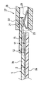
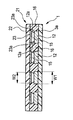
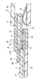
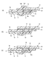
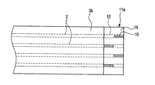
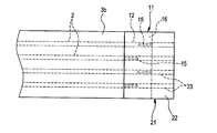
- FIG. 1st embodiment of a flat cable It is a top view which shows 1st embodiment of a flat cable. It is a sectional side view of the flat cable shown in FIG. It is a sectional side view of the connection part of the flat cable and connector shown in FIG. It is a cross-sectional view at one end of the flat cable shown in FIG. It is a sectional side view of the flat cable which concerns on the modification of 1st embodiment. It is a sectional side view which shows 2nd embodiment of a flat cable. It is a sectional side view which shows the modification of 2nd embodiment. It is a perspective view which shows the connection member of this invention. It is a top view of the flat cable which concerns on the modification of this invention. It is a top view of the connection member of the flat cable shown in FIG.
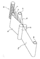
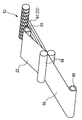
- FIG. It is a top view of the flat cable which concerns on the modification of this invention. It is a top view of the flat cable which concerns on the modification of this invention. It is a top view of the flat cable shown in FIG. It is a perspective view which shows the manufacturing method of a flat cable. It is a top view of the long flat cable in the middle of manufacture. It is a top view of the flat cable in the middle of manufacture. It is a sectional side view of the flat cable in the middle of manufacture. It is a perspective view which shows the other manufacturing method of a flat cable. It is a perspective view which shows the manufacturing method of a elongate connection member. It is a top view which shows the connection member in the middle of manufacture.
- the flat cable 1 includes a plurality of flat conductors 2 made of, for example, rolled copper foil of copper (including plated copper) or copper alloy. These flat conductors 2 are arranged on a plane at a predetermined parallel pitch, and insulating films 3 a and 3 b are bonded (laminated) to the flat conductor 2.
- the number of the rectangular conductors 2 is changed suitably.
- the number of flat conductors 2 may be 20.
- the width dimension, thickness dimension, and parallel pitch of the flat conductor 2 are set according to a required current value or the like.
- the insulating films 3a and 3b are made of a base material part formed from a resin such as polyethylene terephthalate, polyester, polyimide or polyphenylene sulfide, a polyester adhesive or a flame retardant polyvinyl chloride insulating adhesive, a flame retardant polyolefin, or the like. It has the adhesion layer which becomes. Insulating films 3a and 3b are bonded to the flat conductor 2 with the adhesive layer faced. Thus, electrical insulation between the rectangular conductors 2 is achieved.
- the thicknesses of the insulating films 3a and 3b are preferably 0.02 mm or more and 0.15 mm or less, respectively.
- both end portions in the longitudinal direction of the flat cable 1 are formed as longitudinal end portions 11.
- the flat conductor 2 on one side (downward in FIG. 3) of the flat arrangement of the flat conductors 2 is covered with an insulating film 3a.
- the side is not covered with the insulating film 3b and the end portion in the longitudinal direction of the flat conductor 2 is exposed.
- the rectangular conductor 2 exposed at the end 11 in the longitudinal direction is used as the connection electrode 12.
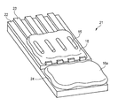
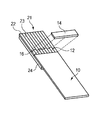
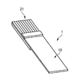
- connection member 21 is connected to the longitudinal end portion 11.
- the connection member 21 is made of, for example, a flat cable, a flexible printed board, a hard board, or the like, and includes a connection base material 22 formed of an insulating material and a plurality of connection conductors 23 provided on the connection base material 22.
- connection base material 22 for example, a film made of polyethylene terephthalate (PET) having a thickness of about 0.25 mm and a polyester adhesive applied to a thickness of about 0.03 mm.
- PET polyethylene terephthalate
- the connection conductors 23 are arranged at the same pitch with substantially the same width dimension W1 as the connection electrodes 12 at the end 11 in the longitudinal direction.
- These connection conductors 23 are made of a rolled copper foil of copper or copper alloy, and the surface thereof is plated with gold.
- connection member 21 is partially overlapped with the longitudinal end portion 11 of the flat cable 1 so that the connection electrode 12 and the connection conductor 23 are electrically connected by the conductive paste 15 and connected to the insulating film 3a.
- the substrate 22 is bonded to the base material 22 with the adhesive 16.
- the conductive paste 15 is applied such that the width dimension W2 in the arrangement direction of the connection electrode 12 and the connection conductor 23 is smaller than the width dimension W1 of the connection electrode 12 and the connection conductor 23.
- the conductive paste 15 is not applied to the end portions (shoulders 12a and 23a) in the width direction of the connection electrode 12 or the connection conductor 23.
- Part of the adhesive 16 also reaches the shoulder 12a or 23a where the conductive paste 15 is not applied. Thereby, the part which the connection electrode 12 and the connection conductor 23 contact with the electrically conductive paste 15 becomes the range below each width dimension.
- an adhesive is filled between the connection electrodes 12 and between the connection conductors 23 so that they are not short-circuited via the conductive paste 15.
- the conductive paste 15 is composed of conductive particles and an adhesive.
- the conductive particles for example, silver powder, carbon powder, copper powder, nickel powder, or a mixed powder thereof can be used.
- the adhesive constituting the conductive paste 15 for example, any of a polyester adhesive, a polyurethane adhesive, an epoxy adhesive, and the like can be used.
- a silver paste containing scaly silver powder having an average particle diameter of 0.5 to 5 ⁇ m and spherical silver powder having an average particle diameter of 20 nm or less coated with an organic substance on the surface is adopted. Is preferred. By including nano silver particles in the silver paste, the connection resistance is lowered, and the surface irregularities are also reduced, thereby increasing the connection area. For this reason, the reliability of electrical connection is improved.
- the adhesive 16 for example, a polyester-based or polyamide-based hot melt adhesive or a thermosetting adhesive having a melting temperature of about 100 to 170 ° C. is used.
- this adhesive 16 JELCONAD-HM6 manufactured by Jujo Chemical Co., Ltd., PES310S30 manufactured by Toa Gosei Co., Ltd., PES375S40 manufactured by the same company, and the like can be used.
- connection member 21 connected to the longitudinal end 11 is inserted into the connector 27, thereby connecting the electrode accommodated in the housing 28 of the connector 27. 29 is brought into pressure contact with the connection conductor 23 of the connection member 21 and is conducted.
- connection conductor 23 of the connection member 21 is gold-plated, a needle-like crystal (whisker) is formed on the surface of the connection conductor 23 even if it receives compressive stress from the connection electrode 29 of the connector 27. Therefore, there is no problem that a short circuit occurs between adjacent connection conductors 23. That is, the reliability of electrical connection with the connector 27 is good.
- FIGS. 5A to 5D show a modification of the flat cable according to the first embodiment.
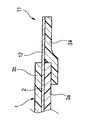
- the protective film 14a is attached to the connection base material 22 side of the connection member 21 so as to straddle the longitudinal direction end 3b1 of the insulating film 3b and the connection member 21. It has been. That is, the protective film 14a covers the connecting member 21 and the insulating film 3b on the same side so as to cover the end of the connecting member 21 on the side affixed to the cable body 10 (the left end of the connecting member 21 in FIG. 5A). Is pasted. Thereby, it is preventing that the cable main body 10 side of the connection member 21 peels.
- the protective film 14b is affixed on the longitudinal direction end part 11 side of the connection member 21 so as to straddle the longitudinal direction end part 12a1 of the connection electrode 12 and the connection member 21. That is, the protective film 14b is affixed to the connection conductor 23 and the insulating film end 3a on the same side so as to cover the longitudinal end 12a1 of the connection electrode 12 and a part of the connection conductor 23. Thereby, it is preventing that the longitudinal direction edge part of the cable main body 10 peels.
- connection member 21 and the cable body 10 are bonded together in a state where the connection body 21 is overlapped so that the cable body 10 side overlaps the cable body 10. .
- the connection member 21 can be firmly affixed to the insulating film 3b of the cable main body 10, and peeling of the connection member 21 is prevented.
- connection base material 22 of the connection member 21 is extended to the cable body 10 side, and only the connection base material 22 is overlapped with the insulating film 3 b of the cable body 10. . That is, the connection conductor 23 is not overlapped with the longitudinal end 3b1 of the insulating film 3b.
- the field where connection conductor 23 does not contribute to electrical connection can be decreased, and flat cable 1 can be provided at low cost.
- a reinforcing film 24 having a rigidity higher than that of the connection base material 22 is attached to the side of the connection base material 22 opposite to the connection conductor 23.
- the connection base material 22 of the connection member 21 and the end portions 22a and 23a on the cable body 10 side of the connection conductor 23 do not overlap the insulating film 3b.
- the reinforcing film 24 includes an extension 24a extending from the end 23a of the connection conductor 23 on the cable body 10 side to a position overlapping the insulating film 3b, and the extension 24a is attached to the insulating film 3b.
- the reinforcing film 24 supports the boundary B between the longitudinal direction end 3b1 of the insulating film 3b and the connection base material 22 with high rigidity.
- the reinforcing film 24 having high rigidity can prevent the bending at the boundary B and can prevent the connection electrode 12 from being disconnected.
- FIG. 6 shows a flat cable 1A according to the second embodiment of the present invention.
- the flat conductor 2 is exposed without the insulating films 3 a and 3 b on both sides of the plane of the flat conductor 2 arranged in a plane.
- the flat conductor 2 exposed at the end in the longitudinal direction is called a connection electrode 12.
- connection member 21 is attached to the longitudinal end portion 11 of the cable body 10 via the adhesive 16, and the connection electrode 12 applies the conductive paste 15. Is connected through the conductor.
- a protective film 14c for protecting the connection electrode 12 and the adhesive 16 is provided on one side (downward in FIG. 6) of the arrangement surface of the connection electrode 12.
- the protective film 14c is attached so as to straddle the connection electrode 12 and the insulating film 3a exposed from the longitudinal ends of the insulating films 3a and 3b.
- the connection electrode 12 and the adhesive 16 applied around the connection electrode 12 are adhered to protect the connection electrode 12.
- the conductive paste 15 has a width dimension in the arrangement direction of the connection electrode 12 and the connection conductor 23 smaller than the width dimension of the connection electrode 12 and the connection conductor 23. It is applied as follows. Thus, the conductive paste 15 is not applied to the end portions (shoulders) in the width direction of the connection electrodes 12 or the connection conductors 23. A part of the adhesive 16 also reaches the shoulder where the conductive paste 15 is not applied. Thereby, the part which the connection electrode 12 and the connection conductor 23 contact with the electrically conductive paste 15 becomes the range below each width dimension. Then, an adhesive is filled between the connection electrodes 12 and between the connection conductors 23 so that they are not short-circuited via the conductive paste 15.
- a reinforcing film 24 is provided on the upper surface of the connection member 21, that is, on the side opposite to the connection conductor 23 of the connection base material 22.
- the reinforcing film 24 has higher rigidity than the connection base material 22.
- the reinforcing film 24 includes an extension 24 a that extends toward the cable body 10 from the end 21 a 1 of the connection member 21 on the cable body 10 side.
- the extension 24 a overlaps the insulating film 3 b of the cable body 10.
- An extension 24a of the reinforcing film 24 is bonded to the insulating film 3b.
- connection electrode 12 of the cable body 10 protrudes from the pair of insulating films 3a and 3b, and the connection electrode 12 may be bent and disconnected at the boundary exposed from the insulating films 3a and 3b. There is. However, since the highly rigid reinforcing film 24 is stuck so as to straddle this boundary portion, the connection electrode 12 can be supported so as not to be bent. Thereby, the flat cable 1A in which the connection electrode 12 is hard to be disconnected can be provided.
- FIGS. 7A to 7C show a modification of the flat cable according to the second embodiment.
- the protective film 14 c is connected to the connection base of the connection member 21 so as to straddle the longitudinal end 3 b 1 of the insulating film 3 b and the connection member 21. It is affixed on the material 22 side. Thereby, it is preventing that the cable main body 10 side of the connection member 21 peels.
- the protective film 14d is affixed on the connection conductor 23 side of the connection member 21 so as to straddle the longitudinal direction end 12a1 of the connection electrode 12 and the connection member 21. Thereby, it is preventing that the longitudinal direction edge part of the cable main body 10 peels.
- This protective film 14d is affixed so as to straddle the connection conductor 23 side of the connection member 21, the opposite side of the exposed connection electrode 12 to the connection member 21, and the insulating film 3a.
- connection member 21 and the cable body 10 are bonded together in a state where the connection body 21 is overlapped with the cable body 10 so as to overlap the cable body 10. .
- the connection member 21 can be firmly affixed to the insulating film 3b of the cable main body 10, and peeling of the connection member 21 is prevented.
- connection base material 22 of the connection member 21 is extended to the cable body 10 side, and only the connection base material 22 is overlapped with the insulating film 3b of the cable body 10. . That is, the connection conductor 23 is not overlapped with the longitudinal end 3b1 of the insulating film 3b.
- a conductive paste is applied to the exposed connection electrode 12 in a region narrower than the width of the connection electrode 12 at the end in the longitudinal direction, and the conductive paste of the connection electrode 12 is not applied to the region.
- the cable body 10 to which an adhesive is applied may be used to affix the longitudinal end of the cable body 10 to a substrate or the like. That is, the connecting member 21 is omitted from the first embodiment and the second embodiment described above, and the cable body 10 in a state where the conductive paste 15 and the adhesive 16 are applied can be connected to a substrate or the like.
- the structure in which the other of the arrangement surface of the connection electrode 12 is exposed and one is covered with the insulating film 3a, or the structure in which both sides of the arrangement surface of the connection electrode 12 are not covered with the insulation film. Can be adopted.
- connection member 21 includes a plurality of connection conductors 23 arranged in a planar shape and a connection base material 22 attached to the connection conductor 23 from one side of the arrangement surface.
- connection conductor 23 On the other side of the arrangement surface of the connection conductors 23, a predetermined region on one end side of the connection conductors 23 is an adhesion region A1.
- the other end portion side of the connection conductor 23 is not an adhesive region.
- the conductive paste 15 is applied to the connection conductor 23 so as to be narrower than the width of the connection conductor 23, as in the first and second embodiments described above.
- an adhesive is applied to the region where the conductive paste 15 on the connection conductor 23 is not deposited and to the connection base material 22.
- connection member 21 has been described with an example in which the connection member 21 includes a plurality of connection conductors 23 that are parallel to each other and have a constant width. As shown in FIGS. 9 and 10, the connection member 21 may include a connection conductor 23 having a linear connection conductor portion 231 and a wide portion 232.
- connection conductor portion 231 of the connection member 21 has a width dimension W4 substantially the same as the width dimension W1 of the connection electrode 12, and
- the pitch of the arrangement is also the same as the pitch of the connection electrodes 12. That is, in this example, the connection conductor portion 231 has a width dimension of 0.2 mm and a parallel pitch of 0.3 mm.
- the wide part 232 has a width dimension W3 larger than the width dimension W4 of the connecting conductor part 231.
- the positions of the wide portions 232 are alternately shifted in a direction orthogonal to the arrangement direction, whereby the wide portions 232 are staggered with a gap between each other on the connection base material 22.
- a connecting conductor portion 231 adjacent to the wide portion 232 of a certain connecting conductor portion 231 has a narrow width at a portion adjacent to the wide portion 232.
- connection conductor parts 231 are arranged on the cable body 10 side, and the wide part 232 is arranged in the insertion / extraction part 21b.
- connection electrode 29 accommodated in the housing 28 of the connector 27 is connected to the connection conductor 23 of the connection member 21 by inserting the connection member 21 into the connector 27. Is brought into pressure contact with the wide portion 232 constituting the conductive portion.
- the connector 27 is alternately staggered in the direction orthogonal to the arrangement direction, and the connector 27 is arranged in a staggered manner.
- connection conductor 23 of the connection member 21 When the connection member 21 is inserted into the connector 27 and connected, the connection conductor 23 of the connection member 21 has a wide portion 232 formed with a width dimension W3 larger than the flat conductor 2 in a direction orthogonal to the arrangement direction. They are staggered by being alternately shifted to each other with a gap between them. For this reason, even if the pitch of the flat conductors 2 of the flat cable 1d is narrow, the connection electrode 29 of the connector 27 can be reliably brought into contact with the wide portion 232 of the connection conductor 23 and can be conducted.
- connection member 21 may be a pitch conversion type connection member formed so that the pitch of the connection conductors 23 is converted in the middle of the flat cable 1 side to the connector 27 side. .
- the connection member 21 may be a pitch conversion type connection member formed so that the pitch of the connection conductors 23 is converted in the middle of the flat cable 1 side to the connector 27 side.
- FIG. 12 shows the cable body 10e to which the connecting member 21 is not connected.
- a portion where one surface of the connection electrode 12 is exposed is referred to as a non-insulating portion (adhesion region) 11a.
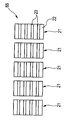
- the conductive paste 15 at each location is applied to 1 ⁇ 2 or less of the length in the longitudinal direction of the connection electrode 12 in the non-insulating portion 11a. Further, in the non-insulating portion 11a, the conductive paste 15 is applied at a position where the conductive electrodes 15 do not overlap in the parallel direction, with the connection electrodes 12 adjacent in the parallel direction.
- the adjacent conductive pastes 15 are 1 ⁇ 2 the length of the connection electrode 12 in the non-insulating portion 11a, and are arranged in a staggered manner by alternately shifting their longitudinal positions. ing.
- the adhesive 16 is applied to the part where the conductive paste 15 is not applied. That is, when the non-insulating portion 11a is scanned from one end to the other end in the longitudinal direction when the non-insulating portion 11a is viewed in the parallel direction of the connection electrode 12 (see FIG. 12 from above or below), 15 is applied to at least one connection electrode 12. In other words, when the non-insulated portion 11a is viewed in the parallel direction of the connection electrode 12 over the entire area of the non-insulated portion 11a, there is no portion where the conductive paste 15 is not applied.
- connection member 21 is superimposed on the non-insulated portion 11 a of the cable body 10 e to form a flat cable 1 e, and the connection electrode 12 and the connection conductor 23 are conductively connected via the conductive paste 15. The Further, the connection member 21 is bonded to the non-insulating portion 11 a with the adhesive 16 around the conductive paste 15.
- the conductive paste 15 has a width dimension in the arrangement direction of the connection electrode 12 and the connection conductor 23 smaller than the width dimension of the connection electrode 12 and the connection conductor 23. It is applied to become.
- the conductive paste 15 has a weaker adhesive strength than the adhesive 16. Therefore, when the conductive paste 15 is applied to each connection electrode 12 over the entire length in the longitudinal direction in the non-insulated portion 11a, the conductive connection portion between the connection electrode 12 and the connection conductor 23 when the connection member 21 is bonded. In such a case, sufficient adhesive strength cannot be obtained, and adhesion failure may occur.
- connection member 21 when the connection member 21 is bonded, the conductive paste 15 is crushed by the connection electrode 12 and the connection conductor 23 and spreads to the side, and the adjacent conductive pastes 15 may come into contact with each other to cause a short circuit. .
- the short circuit due to the contact between the conductive pastes 15 is likely to occur particularly when the arrangement of the flat conductors 2 is a narrow pitch (for example, 0.4 mm or less).
- the conductive paste 15 is applied to 1 ⁇ 2 or less of the length of the connection electrode 12.
- the adhesion area by the adhesive agent 16 between the connection member 21 and the longitudinal direction edge part 11 of the cable main body 10 can be ensured enough, and troubles, such as adhesion failure, can be eliminated.
- the usage-amount of the electrically conductive paste 15 can be reduced. It should be noted that conduction between the connection electrode 12 and the connection conductor 23 by the conductive paste 15 can be sufficiently ensured even with a small contact area.
- the conductive paste 15 is applied to the adjacent connection electrode 12 at a position where the conductive paste 15 does not overlap in the parallel direction, the conductive paste between the connection electrode 12 and the connection conductor 23 when the connection member 21 is bonded. Even if 15 is crushed and spreads to the side, it is possible to eliminate the problem that adjacent conductive pastes 15 come into contact with each other and short-circuit.
- the adhesive 16 is applied to a portion of the non-insulating portion 11a where the conductive paste 15 is not applied, and the conductive paste 15 is applied to any of the connection electrodes 12 from one end to the other end in the longitudinal direction. Therefore, the application area of the adhesive 16 is partitioned by the conductive paste 15.
- connection member 21 can be strongly bonded and fixed, and the connection electrode 12 and the connection conductor 23 are conductively connected without a short circuit due to contact between the conductive pastes 15. It can be set as the flat cable 1e.
- the rectangular conductors 2 are sent out from a plurality of reels 30 around which the long rectangular conductors 2 are wound, and arranged on the same plane at a predetermined parallel pitch. Then, a pair of long insulating films 3a and 3b are fed from the reel 31 to the front and back of the arrangement surface of these rectangular conductors 2 and passed between the heater rollers 32 to heat and heat the insulating films 3a and 3b at the same time and bonded together.
- the long flat cable 10a The long flat cable 10 a is wound around the winding roller 33.
- a window portion 35 is formed in a part of the insulating film 3b in the longitudinal direction.
- the long flat cable 10a is cut at a position indicated by a chain line C1. Thereby, the location where the insulating film 3a and the insulating film 3b were connected to the longitudinal direction in the width direction both ends of the window part 35 is removed.
- the long flat cable 10a is cut at a position indicated by a chain line C2 passing through the center of the window portion 35 to have a predetermined length as shown in FIGS. 16 and 17, and the rectangular conductor 2 is formed at both ends in the longitudinal direction.
- the cable body 10 is formed with the connection electrode 12 exposed on one side.
- a long flat cable 10a having no window portion is prepared, and the short flat cable 10b is formed by cutting this into a desired length.
- the cable body 10 may be created by peeling off a part of the insulating film 3b from the end of 10b.
- connection member 21 is created.
- the rectangular conductors 61 are fed out from a plurality of reels 62 around which a plurality of long rectangular conductors 61 to be the connection conductors 23 are wound, and are arranged on the same plane at a predetermined parallel pitch.
- a long connecting base material 22 such as a polyethylene terephthalate (PET) film is fed from the reel 63 to one side of these flat conductors 61 and is passed between the heater rollers 64 to heat the connecting base material 22 and at the same time the flat conductor 61. Apply pressure to the tape. Further, the exposed surface of the flat conductor 61 affixed to the connection base material 22 is plated with gold to produce a long connection member 21 a, and the long connection member 21 a is wound around a winding roller 66. After that, as shown in FIG. 20, the long connecting member 21a is cut by a cutter such as a cutter every predetermined length to create the connecting member 21.
- a cutter such as a cutter every predetermined length to create the connecting member 21.
- the conductive paste 15 is applied to the connection electrode 12 made of the flat conductor 2, and the adhesive 16 is applied on the insulating film 3a on both sides of the connection electrode 12 in the width direction.
- the conductive paste 15 and the adhesive 16 are applied to the longitudinal end portion 11 by transfer.
- a conductive paste 15 is applied at a predetermined pitch to a transfer release film 51 formed from a resin such as polyethylene terephthalate (PET), and the conductivity of the release film 51 is also determined.
- a transfer film 52 in which the adhesive 16 is applied to the side of the paste 15 is prepared.
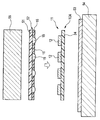
- the transfer film 52 is superposed on the longitudinal end 11 of the cable body 10 and placed on the surface plate 54 via the cushion material 53, and the heat tool 55 is lightly pressed from above and heated. In this way, the top of the conductive paste 15 is pressed against the connection electrode 12 and crushed and flattened. Also, the adhesive 16 on the transfer film 52 side is softened by heat and peeled off from the release film 51, and the cable body. 10 on the insulating film 3a or on the connection electrode 12.
- the cable body 10 is taken out and the release film 51 of the transfer film 52 is peeled off as shown in FIG. Then, the cable body 10 in which the conductive paste 15 is provided on the connection electrode 12 so as to protrude in the opposite direction to the insulating film 3 a, and a part of the adhesive 16 is also applied on the shoulder 12 a of the connection electrode 12. Is obtained.
- the conductive paste 15 and the adhesive 16 can be applied by arranging the insulating film 3a on the lower side and applying the conductive paste 15 and the adhesive 16. The conductive paste 15 and the adhesive 16 are prevented from flowing down.
- connection member 21 is connected to the longitudinal end portion 11 of the cable body 10.
- the connection member 21 includes a connection base material 22 and a plurality of connection conductors 23 bonded to the connection base material 22.
- the connection conductors 23 are arranged at substantially the same width and the same pitch as the connection electrodes 12 of the cable body 10 and are plated with gold.
- the connecting member 21 is overlapped with the longitudinal end portion 11 of the cable body 10.
- the exposed connection electrodes 12 are overlapped so as to be completely covered with the connection conductors 23.
- the connection electrode 12 and the connection conductor 23 are conducted by the conductive paste 15, and the insulating film 3 a and the connection base material 22 are bonded by the adhesive 16.
- a part of the adhesive 16 is spread between the connection electrode 12 and the connection conductor 23, whereby the connection electrode 12 and the connection conductor 23 are bonded by the adhesive 16.
- the flat cable 1 shown in FIG.1, FIG.2, etc. is produced by affixing the connection member 21 on the cable main body 10.
- connection base material 22 of the connection member 21 is transparent, when connecting the cable main body 10 and the connection member 21, it superimposes so that the connection member 21 may be covered with respect to the cable main body 10 from upper direction. Is preferred. In this way, the positions of the connection conductor 23 and the connection electrode 12 can be visually determined or automatically determined by the electronic device as image data through the transparent connection member 21 from above and can be aligned.
- connection member 21 When the insulating film 3a is transparent, when connecting the cable body 10 and the connection member 21, it is preferable to overlap the connection member 21 so as to cover the cable body 10 from above. If it does in this way, the position of the connection electrode 12 and the connection conductor 23 can be visually determined from the upper side through the transparent insulating film 3a of the cable main body 10 or automatically as image data by the electronic device and can be aligned. .
- connection electrode 12 and the connection conductor 23 are visually aligned through the transparent protective film 14 and the transparent insulating film 3a. Can do.
- connection member 21 When the connection member 21 is bonded to the longitudinal end 11 of the cable body 10, the connection member 21 is first connected to the conductive paste 15 protruding from the adhesive 16 as shown in FIG. The conductor 23 comes into contact with the connection electrode 12 and the connection conductor 23 to ensure conduction. Further, when the connection member 21 is pressed against the longitudinal end portion 11 of the cable body 10, the conductive paste 15 is sandwiched between the connection electrode 12 and the connection conductor 23 and crushed as shown in FIG. . As a result, the conductive paste 15 is in good contact with the connection conductor 23.
- the width dimension W2 of the conductive paste 15 is smaller than the width dimension W1 of the connection electrode 12 and the connection conductor 23 (see FIG. 4), even if the conductive paste 15 is crushed and spread to the side, Even if it is within the range of the width of the connection electrode 12 or the connection conductor 23 or slightly protrudes, it is pressed into the adhesive 16 and does not reach the adjacent connection electrode 12 or connection conductor 23. That is, the trouble that the conductive paste 15 short-circuits between the adjacent connection electrodes 12 or between the adjacent connection conductors 23 is also prevented.
- the insulating film 3a of the cable body 10 is formed by laminating a base layer 3a2 and an adhesive layer 3a1 provided on the base layer 3a2. The whole is heated when the connecting member 21 is bonded to the longitudinal end 11 of the cable body 10.
- the adhesive layer 3a1 at the longitudinal end portion 11 of the cable body 10 is softened by heating, and the connection electrode 12 at the longitudinal end portion 11 sinks into the adhesive layer 3a1 by receiving a force for bonding the connecting member 21. Accordingly, the adhesive 16 rises between the connection electrodes 12 at the longitudinal ends 11, the adhesive 16 enters between the connection conductors 23 of the connection member 21, and contacts the connection base material 22 of the connection member 21. Thereby, the connection member 21 is satisfactorily connected to the cable body 10 without problems such as adhesion failure and short circuit.
- connection member 21 is an example, and other connection methods may be used.
- connection member 21 is manufactured from a flexible printed board or a hard board, a conductor pattern to be the connection conductor 23 is formed by etching or the like, and then the conductor pattern is plated with gold.
- the conductive paste 15 and the adhesive 16 may be applied to the connection member 21.
- the connection member 21 As a method of applying the conductive paste 15 and the adhesive 16 to the connecting member 21, transfer or direct printing can be used.
- the connection member 21 is bonded in the position which straddles the boundary B of the insulating film 3b. Thereby, as shown in FIG. 5B, the vicinity of the connection electrode 12 in the vicinity of the boundary B that is easily bent can be reinforced.
- the conductive paste 15 is not applied to the end portion on the flat cable 1 side, and the adhesive 16 is applied to the end portion 21 a 2 on the flat cable 1 side of the connecting member 21. .
- the end of the connecting member 21 on the flat cable 1 side is bonded to the upper surface of the insulating film 3b of the flat cable 1 via the adhesive 16, and the connecting member 21 can be made difficult to peel off from the flat cable 1.
- connection base material 22 transparent because the alignment between the connection conductor 23 and the connection electrode 12 is facilitated.
- a flat cable was prepared by the above manufacturing method and subjected to a high temperature test.
- the change of the resistance value was measured by placing the flat cable in a constant temperature bath at 85 ° C. for 500 hours. As a result, the resistance value did not increase even after 500 hours.
- the resistance value increases. It was confirmed that the connecting member was securely bonded to the cable body even when exposed to the bottom.
- one side of the arrangement surface of the flat conductors 2 is covered with the insulating film 3a, and the other side is not covered with the insulating film 3b.
- the manufacturing method for creating the flat cable 1 has been described.
- a manufacturing method of the flat cable 1A of the second embodiment in which both sides of the arrangement surface of the rectangular conductors 2 are not covered with the insulating films 3a and 3b at the longitudinal end portion 11 will be described.
- the manufacturing method according to this embodiment is substantially the same as the manufacturing method of the first embodiment described above, and different points will be described below.
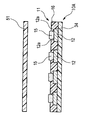
- an additional film 34 is attached to one side of the arrangement surface (lower side in FIG. 27).
- the additional film 34 is attached so as to straddle the entire lower surface of the exposed connection electrode 12 and the insulating film 3a. Thereby, the exposed connection electrode 12 is fixed on the additional film 34.
- a conductive paste 15 is applied at a predetermined pitch to a transfer release film 51 formed from a resin such as polyethylene terephthalate (PET), and the conductive paste 15 of the release film 51 is applied.
- a transfer film 52 in which the adhesive 16 is applied to the side portions of is prepared.
- the transfer film 52 is superposed on the longitudinal end 11 of the cable body 10A, placed on the surface plate 54 via the cushion material 53, and heated by lightly pressing the heat tool 55 from above. In this way, the top of the conductive paste 15 is pressed against the connection electrode 12 and crushed and flattened. Also, the adhesive 16 on the transfer film 52 side is softened by heat and peeled off from the release film 51, and the cable body. It descends on the additional film 34 of 10A or on the connection electrode 12.
- connection electrode 12 is provided on the connection electrode 12 so as to protrude in the opposite direction to the additional film 34, and a part of the adhesive 16 is also disposed on the shoulder 12 a of the connection electrode 12.
- a cable main body 10A is obtained.
- connection member 21 is connected to the longitudinal end portion 11 of the cable body 10A.
- the connection member 21 includes a connection base material 22 and a plurality of connection conductors 23 bonded to the connection base material 22.
- the connection conductors 23 are arranged at substantially the same width and the same pitch as the connection electrodes 12 of the cable body 10A, and are plated with gold.
- the connecting member 21 is overlapped with the longitudinal end portion 11 of the cable body 10A.
- the connection electrodes 12 are overlapped so as to be completely covered with the connection conductors 23.
- the connection electrode 12 and the connection conductor 23 are electrically connected by the conductive paste 15, and the additional film 34 and the connection base material 22 are bonded by the adhesive 16.
- a part of the adhesive 16 extends between the connection electrode 12 and the connection conductor 23, and the connection electrode 12 and the connection conductor 23 are bonded to each other by the adhesive 16.
- the additional film 34 is transparent, when connecting the cable body 10A and the connection member 21, it is preferable to overlap the connection member 21 so as to cover the cable body 10A from above. If it does in this way, the position of the connection electrode 12 and the connection conductor 23 can be visually observed and aligned through the transparent additional film 34 of 10 A of cable main bodies from the upper side.
- connection member 21 When the connection member 21 is bonded to the longitudinal end 11 of the cable body 10A, first, as shown in FIG. 33A, the connection member 21 is connected to the conductive paste 15 protruding from the adhesive 16. The conductor 23 comes into contact with the connection electrode 12 and the connection conductor 23 to ensure conduction. Further, when the connection member 21 is pressed against the longitudinal end portion 11 of the cable body 10A, the conductive paste 15 is sandwiched between the connection electrode 12 and the connection conductor 23 and crushed as shown in FIG. . As a result, the conductive paste 15 is in good contact with the connection conductor 23.
- the width dimension W2 of the conductive paste 15 is smaller than the width dimension W1 of the connection electrode 12 and the connection conductor 23, even if the conductive paste 15 is crushed and spread to the side, the connection electrode 12 or the connection Even if it is within the width of the conductor 23 or slightly protrudes, it is pressed into the adhesive 16 and does not reach the adjacent connection electrode 12 or connection conductor 23. That is, the trouble that the conductive paste 15 short-circuits between the adjacent connection electrodes 12 or between the adjacent connection conductors 23 is also prevented.
- the additional film 34 includes a base layer 34a2 and an adhesive layer 34a1 provided on the base layer 34a2.
- the adhesive layer 34a1 of the additional film 34 is softened by heating, and the connection electrode 12 at the longitudinal direction end portion 11 sinks into the adhesive layer 34a1 under the force that the connection member 21 is bonded. Accordingly, the adhesive 16 rises between the connection electrodes 12 at the longitudinal ends 11, the adhesive 16 enters between the connection conductors 23 of the connection member 21, and contacts the connection base material 22 of the connection member 21. Thereby, the connecting member 21 is connected to the cable main body 10A satisfactorily without problems such as adhesion failure and short circuit.
- connection conductor 23 of the connection member 21 is gold-plated, it is possible to manufacture a flat cable that has high reliability of electrical connection while suppressing cost as much as possible and that is free from defects such as poor adhesion to the connection member 21. it can.
- the additional film 34 is attached to one surface of the connection electrode 12 made of the flat conductor 2 protruding from the insulating films 3a and 3b, and then the conductive paste 15 is applied to the connection electrode 12 to connect the additional film 34 to the connection electrode. Since the adhesive 16 is applied to the side of the conductive paste 15, the conductive paste 15 and the adhesive 16 can be applied satisfactorily without flowing down, and the workability is good.
- the example in which the conductive paste 15 and the adhesive 16 are applied to the longitudinal end portion 11 of the cable body 10 ⁇ / b> A has been described.
- the conductive paste 15 and the adhesive 16 are applied to the connection member 21. It may be applied.
- the flat cable 1 can be produced by creating the cable body 10 by peeling 3a and 3b and attaching the connecting member 21 to the longitudinal end 11 thereof.
- FIG. 34 to 35 are diagrams for explaining a method of applying the conductive paste 15 and the adhesive 16 to the connecting member 21.
- FIG. 34 to 35 are diagrams for explaining a method of applying the conductive paste 15 and the adhesive 16 to the connecting member 21.
- the reinforcing film 24 is attached to the connection base material 22 on the opposite side of the connection conductor 23 of the connection member 21 cut into a desired length. At this time, the reinforcing film 24 is pasted so that a part thereof protrudes from the end portion in the longitudinal direction of the connection conductor 23.
- the conductive paste 15 is applied to the upper surface of the connection conductor 23 of the connection member 21, and the adhesive 16 is applied to the region of the upper surface of the connection member 21 excluding the conductive paste 15. .
- the conductive paste 15 is thinner than the width dimension of the connection electrode 12 and the connection conductor 23 and is higher than the adhesive 16.
- the adhesive 16 a is also applied to the upper surface of the reinforcing film 24 (the surface on the same side as the connection conductor 23). As shown in FIGS.
- the length of the region where the conductive paste 15 is applied is set to 1 ⁇ 2 or less of the length of the non-insulating portion (adhesion region) 11 a of the cable body 10, and
- the conductive paste 15 may be applied between the matching connection conductors 23 so that the positions in the length direction do not overlap each other.
- the longitudinal end of the insulating film 3b of the cable body 10 is attached to the reinforcing film 24 with an adhesive 16a so that the connection electrode 12 and the connection conductor 23 are conducted through the conductive paste 15. wear. As a result, the longitudinal end portion 11 of the cable body 10 is bonded to the connection member 21.
- the reinforcing film 24 is attached to the insulating film 3b so that the extension 24a straddles the end 22a of the connection base material 22 on the cable body 10 side and the end of the insulating film 3b. It is done.
- the protective film 14 is applied to the exposed connection electrode 12 so that the state where the connection electrode 12 and the connection conductor 23 are conducted through the conductive paste 15 is maintained by the adhesive 16. Adhering and protecting the surfaces of the connection electrode 12 and the adhesive 16 are performed. Thereby, the flat cable 1 as shown in FIG. 38 is completed.
- the width dimension W2 of the conductive paste 15 is applied to be smaller than the width dimension W1 of the connection electrode 12 and the connection conductor 23 (see FIG. 35), the conductive paste 15 is crushed side by side. Even if it spreads out, it is within the range of the width of the connection electrode 12 or connection conductor 23, or even if it protrudes somewhat, it is pressed into the adhesive 16 and does not reach the adjacent connection electrode 12 or connection conductor 23. That is, the trouble that the conductive paste 15 short-circuits between the adjacent connection electrodes 12 or between the adjacent connection conductors 23 is also prevented.
- the conductive paste 15 and the adhesive 16 can be directly applied to the connection member 21 without using a transfer film or the like, so that workability is good.
- the extension part 24a of the reinforcement film 24 is insulated from the edge part 22a by the side of the cable main body 10 of the connection base material 22. It affixes on the upper surface of the insulating film 3b so that the boundary B with the longitudinal direction edge part 3b1 of the film 3b may be straddled. For this reason, it becomes difficult to bend at the boundary B, and it can be prevented from being bent at the boundary B in the process of applying the protective film 14. For this reason, it is possible to prevent the flat conductor 2 of the cable body 10 from being disconnected at the boundary B.
- connection conductor 23 is gold-plated in the state of the long connection member 21a. For this reason, a whisker is not generated between the flat conductor 2 and the connection conductor 23, and the flat cable 1 with high electrical connection reliability can be provided.
- gold plating can be performed at low cost by performing gold plating on the connection conductor 23 in the state of the long connection member 21a.
- the entire length of the flat conductor 2 is gold-plated when the long flat cable 10a is formed, so that the plating covered with the insulating films 3a and 3b is unnecessary. It is not realistic because the part is long.
- the connecting conductor 23 is continuously plated with gold in the state of the long connecting member 21a, and then cut into a necessary length. Therefore, it is possible to perform gold plating at a low cost by continuous treatment, and furthermore, it is possible to perform gold plating only on necessary portions. Thereby, the high quality flat cable 1 can be provided at low cost.
- connection conductor 23 since gold plating is performed after the connection conductor 23 is attached to the connection base material 22, the portion of the connection conductor 23 that contacts the connection base material 22 is not gold-plated. Therefore, the flat cable 1 can be provided at a low cost because the portion that does not require gold plating is not gold plated. If there is no risk of damage due to whiskers, such as when the distance between conductors is wide, tin plating or the like may be applied to the connection conductor 23 instead of gold plating.
- connection member 21 is attached to the longitudinal end portion 11 of the cable body 10 after the reinforcement film 24 is attached to the connection base material 22 . It is not limited to this example.
- the reinforcing film 24 is simultaneously straddled across the connection base material 22 and the insulating film 3 a of the cable body 10. You may paste as follows.
- connection base material 22 transparent because the alignment between the connection conductor 23 and the connection electrode 12 is facilitated.
- connection member 21 includes a plurality of connection conductors 23 that are parallel to each other and have a constant width.
- the present invention is not limited to these examples.
- the connection member 21 including the connection conductor 23 having the linear connection conductor portion 231 and the wide portion 232 may be employed.
- the example in which the adhesive 16 is applied around the conductive paste 15 has been described.
- the insulating film 3 a of the cable body 10 is attached with the connection electrode 12.
- an adhesive layer 3a1 is provided.
- the adhesive constituting the adhesive layer 3a1 wraps around the conductive paste 15 and prevents the adjacent conductive pastes 15 from adhering to each other.
- the additional film 34 includes an adhesive layer 34 a 1 for attaching the connection electrode 12. For this reason, when bonding the connection member 21 to the cable body 10, the additional film 34 and the connection member 21 may be bonded together by the adhesive layer 34 a 1 without applying the adhesive 16. Even in this case, the adhesive constituting the adhesive layer 34a1 is prevented from flowing around the conductive paste 15 and adjoining the conductive paste 15 to each other.
- connection base material 22 of the connection member 21 includes an adhesive layer 22a1 and a base material 22a2 for attaching the connection conductor 23 thereto. For this reason, when bonding the connection member 21 to the cable body 10, the cable body 10 and the connection member 21 may be bonded by the adhesive layer 22 a 1 without applying the adhesive 16. Even in this case, the adhesive constituting the adhesive layer 22a1 is prevented from flowing around the conductive paste 15 and adhering to each other.
- FIG. 39 is a plan view showing a transfer film 52 on which the conductive paste 15 and the adhesive 16 to be transferred to the connection electrode 12 or the connection conductor 23 are stacked.
- the transfer film 52 includes a resin film 51, a conductive paste 15 and an adhesive 16 applied on the resin film 51.
- the conductive paste 15 is applied to the resin film 51 at a predetermined pitch along a first direction that is orthogonal to the longitudinal direction of the connection electrode 12 or the connection conductor 23. Further, an adhesive is applied around the conductive paste 15 on the resin film 51. The conductive paste 15 adjacent along the first direction is applied so that the positions in the second direction orthogonal to the first direction do not overlap.
- the adhesive 16 is applied to a portion where the conductive paste 15 is not applied.
- the conductive paste 15 and the adhesive 16 are applied to the longitudinal end portion 11 of the cable body 10 using such a transfer film 52, the adjacent conductive properties as shown in FIGS.
- the cable main body 10 and the flat cable 1 having the conductive pastes 15 arranged in a staggered pattern in which the positions in the longitudinal direction of the pastes 15 are staggered can be created.
- the connection member 21 may be produced using the transfer film 52 or by direct printing.
- Japanese patent applications filed on June 16, 2011 Japanese Patent Application 2011-133865
- Japanese patent applications filed on June 16, 2011 Japanese Patent Application 2011-133951
- Japanese patent application (Japanese Patent Application 2011-134156) Japanese patent application filed on June 16, 2011 (Japanese Patent Application 2011-134476), Japanese patent application filed on June 1, 2012 (Japanese Patent Application 2012-125676), 2012 Based on Japanese patent application filed on June 1, 2012 (Japanese Patent Application No. 2012-125686) and Japanese patent application filed on June 12, 2012 (Japanese Patent Application No. 2012-132727), the contents of which are hereby incorporated by reference It is captured.
- the conductive paste is applied in a region narrower than the width of the conductor, so that adjacent conductive pastes adhere to each other when the connecting member is bonded to the cable body. There is no short circuit between the conductors. Therefore, a flat cable that can be satisfactorily connected to the flat cable of the connection partner without a short circuit defect is provided.
Landscapes
- Engineering & Computer Science (AREA)
- Microelectronics & Electronic Packaging (AREA)
- Insulated Conductors (AREA)
Abstract
Description
平面状に配列された複数本の導体の両面に絶縁フィルムが貼り合わされて、その長手方向端部で前記導体の一部は前記絶縁フィルムで覆われていないケーブル本体と、
前記導体と同数の接続導体に接続基材が貼り付けられた接続部材を備え、
前記接続部材は、その一部が前記ケーブル本体の長手方向端部に接着剤によって貼り付けられており、
前記導体は、前記接続導体に導電性ペーストを介して接続されており、
前記導電性ペーストは、前記導体の幅よりも細い領域内に塗布されていることを特徴とする。
前記ケーブル本体の長手方向端部において、前記導体の平面状に配列された配列面の一方側は前記絶縁フィルムで覆われており、配列面の他方側は前記絶縁フィルムで覆われていない構成としてもよい。
前記ケーブル本体の長手方向端部において、前記導体がいずれの前記絶縁フィルムにも覆われていない構成としてもよい。
前記導電性ペーストの塗布された領域の長さは、前記絶縁フィルムの長手方向端部から露出された前記導体の長さの1/2以下であり、
隣り合う前記導体の間で、それぞれの前記導電性ペーストは、前記長手方向の位置が互いに重ならない構成としてもよい。
前記接続導体は、前記導体よりも大きな幅寸法を有する幅広部と、前記幅広部よりも小さい幅寸法を有する幅狭部とを有し、
隣り合う前記接続導体の間で、前記幅広部は、長手方向の位置が互いに重ならない構成としてもよい。
複数の前記接続導体の間のピッチが途中で変えられていてもよい。
前記ケーブル本体に貼られた側の前記接続部材の端を覆うように、前記接続部材および同側の前記絶縁フィルムに保護フィルムが貼り付けられていてもよい。
前記導体の長手方向端部と前記接続導体の一部とを覆うように、前記接続導体および同側の前記絶縁フィルム端部に保護フィルムが貼り付けられていてもよい。
前記導体の前記配列面の他方の側に前記接続部材が貼り付けられており、
前記導体の前記配列面の一方の側に、前記導体を覆う保護フィルムが貼り付けられていてもよい。
前記接続基材の前記接続導体とは反対側に、前記接続基材よりも剛性の高い補強フィルムが貼り付けられていてもよい。
前記補強フィルムは、前記接続導体および前記接続基材よりも前記ケーブル本体側に延びた延長部を有し、
前記延長部が前記絶縁フィルムに貼り付けられていてもよい。
前記絶縁フィルムおよび前記接着剤は透明であってもよいし、前記接続基材および前記接着剤が透明であってもよい。
平面状に配列された複数本の導体と、
複数の前記導体の両面に貼り合わされた絶縁フィルムとを備え、その長手方向端部で前記導体の片面または両面が前記絶縁フィルムで覆われていないケーブル本体であって、
前記ケーブル本体の長手方向端部において、
前記導体には、前記導体の幅よりも細い領域内に導電性ペーストが塗布されており、
前記導体上の前記導電性ペーストが塗布されていない領域には接着剤が付着されていることを特徴とする。
前記ケーブル本体の前記長手方向端部において、前記導体は配列面の一方側は前記絶縁フィルムで覆われており、配列面の他方側は前記導体が前記絶縁フィルムで覆われていない構成としてもよい。
前記ケーブル本体の前記長手方向端部において、前記導体が配列面の両側で前記絶縁フィルムに覆われていない構成としてもよい。
前記導電性ペーストの塗布された領域の長さは、前記絶縁フィルムの長手方向端部から露出された前記導体の長さの1/2以下であり、
隣り合う前記導体の間で、それぞれの前記導電性ペーストは、前記長手方向の位置が互いに重ならない構成としてもよい。
平面状に配列された複数本の接続導体と、
配列面の一方の側から接着剤層を介して前記接続導体に貼り付けられた接続基材とを備え、
前記接続導体の配列面の他方の側において、前記接続導体の一方の端部から延びる所定の領域が接着領域とされており、前記接着領域において、
前記接続導体には前記接続導体の幅より細く導電性ペーストが塗布されており、
前記接続導体上の前記導電性ペーストが塗布されていない領域に接着剤が付着していることを特徴とする。
前記導電性ペーストの塗布された領域の長さは、前記接着領域の長さの1/2以下であり、
隣り合う前記接続導体の間で、それぞれの前記導電性ペーストは、長手方向の位置が互いに重ならない構成としてもよい。
前記接続導体は、前記導体よりも大きな幅寸法を有する幅広部と、前記幅広部よりも小さい幅寸法を有する幅狭部とを有し、
隣り合う前記接続導体の間で、前記幅広部は、長手方向の位置が互いに重ならない構成としてもよい。
複数の前記接続導体の間のピッチが途中で変えられていてもよい。
前記接続基材の前記接続導体とは反対側の面に、前記接続基材よりも剛性の高い補強フィルムが貼られていてもよい。
前記接続導体には、前記接続導体の長手方向の一方側に前記導電性ペーストが塗布され、他方側で前記導電性ペーストが塗布されておらず、
前記補強フィルムは、前記接続導体の長手方向に関して前記接続導体に前記導電性ペーストが塗布された側で、前記接続導体よりも延びた延長部を備えていてもよい。
樹脂フィルムと、前記樹脂フィルム上に第1の方向に沿って複数箇所に所定のピッチで塗布された導電性ペーストと、前記樹脂フィルム上における前記導電性ペーストの周囲に塗布された接着剤とを有する転写部材であって、
前記第1の方向に沿って隣り合う前記導電性ペーストは、前記第1の方向と直交する第2の方向の位置が重ならず、
前記接着剤は、前記導電性ペーストが塗布されていない部分に塗布されていることを特徴とする。
平面状に配列された複数本の導体の両面に絶縁フィルムが貼り合わされていて長手方向の両端で前記導体の片面または両面が露出したケーブル本体を用意し、
前記導体と同数の接続導体に接続基材が貼り付けられた接続部材を用意し、
前記ケーブル本体と前記接続部材とが向かい合う領域において、導電性ペーストを各々の前記導体の幅よりも細い領域内に塗布し、
前記導体と前記接続導体とを前記導電性ペーストを介して導通接続し、前記絶縁フィルムと前記接続基材とを接着剤を介して接続するように、前記ケーブル本体の長手方向端部に前記接続部材の一部を貼り合せることを特徴とする。
前記ケーブル本体の長手方向端部において、前記導体の配列面の一方側の前記絶縁フィルムが前記導体を覆わないケーブル本体を用意し、
前記ケーブル本体と前記接続部材とが向かい合う領域において、
各々の前記導体に前記導電性ペーストを塗布し、
前記導体上の前記導電性ペーストが塗布されない部分の前記導体に前記接着剤を塗布してもよい。
前記ケーブル本体の長手方向端部において、前記導体の配列面の一方側の前記絶縁フィルムが前記導体を覆わない前記ケーブル本体を用意し、
前記ケーブル本体と前記接続部材とが向かい合う領域において、
各々の前記接続導体に前記導電性ペーストを塗布し、
前記接続導体上の前記導電性ペーストが塗布されない部分の前記接続導体に前記接着剤を塗布してもよい。
前記ケーブル本体の長手方向端部において、前記導体の配列面の両側の前記絶縁フィルムが前記導体を覆わない前記ケーブル本体を用意し、
前記導体の配列面の一方の側に付加フィルムを貼り付け、
各々の前記導体に前記導電性ペーストを塗布し、
前記導体上の前記導電性ペーストが塗布されない部分の前記導体に前記接着剤を塗布してもよい。
前記ケーブル本体の長手方向端部において、前記導体の配列面の両側の前記絶縁フィルムが前記導体を覆わない前記ケーブル本体を用意し、
前記導電性ペーストを前記接続導体に塗布し、前記接着剤が前記接続導体上の前記導電性ペーストを塗布されない部分の前記接続導体に塗布し、前記接続部材を前記ケーブル本体の前記長手方向端部に貼り付けてもよい。
前記導電性ペーストを塗布する領域の長さを前記絶縁フィルムの長手方向端部から露出された前記導体の長さの1/2以下とし、隣り合う前記導体の間でそれぞれの前記導電性ペーストが前記長手方向の位置が互いにずれるように、前記導電性ペーストを塗布してもよい。
前記接続導体は、前記導体よりも大きな幅寸法を有する幅広部と、前記幅広部よりも小さい幅寸法を有する幅狭部とを有し、
隣り合う前記導体の間で、前記幅広部は、長手方向の位置が互いに重ならないようにしてもよい。
複数の前記接続導体の間のピッチが途中で変えられていてもよい。
前記ケーブル本体に貼られた側の前記接続部材の端を覆うように、前記接続基材および同側の前記絶縁フィルムに保護フィルムを貼り付けてもよい。
前記導体の長手方向端部と前記接続導体の一部とを覆うように、前記接続導体および同側の前記絶縁フィルム端部に保護フィルムを貼り付けてもよい。
前記導電性ペーストを塗布する前に、前記接続基材の前記接続導体とは反対側に、前記接続基材よりも剛性の高い補強フィルムを貼り付けてもよい。
<第一実施形態>
以下、本発明に係るフラットケーブルの第一実施形態の例を、図面を参照して説明する。
図1及び図2に示すように、フラットケーブル1は、例えば、銅(メッキされた銅を含む)または銅合金の圧延銅箔からなる複数本の平角導体2を備えている。これらの平角導体2は、所定の並列ピッチで平面上に配列されており、平角導体2に絶縁フィルム3a,3bが貼着(ラミネート)されている。なお、図1では平角導体2を4本有する例を示しているが、平角導体2の本数は適宜変更される。例えば、平角導体2を20本とすることもできる。また、平角導体2の幅寸法、厚さ寸法及び並列ピッチは、要求される電流値等に合わせて設定される。
フラットケーブル1の長手方向端部11では、平角導体2の平面状に配列された配列面の一方側(図3において下方)の平角導体2は絶縁フィルム3aで覆われており、配列面の他方側は絶縁フィルム3bに覆われておらず平角導体2の長手方向端部が露出されている。この長手方向端部11で露出された平角導体2が接続電極12とされている。
また、保護フィルム14bが、接続電極12の長手方向端部12a1と接続部材21とを跨ぐように、接続部材21の長手方向端部11側に貼り付けられている。つまり、接続電極12の長手方向端部12a1と接続導体23の一部とを覆うように、接続導体23および同側の絶縁フィルム端部3aに保護フィルム14bが貼り付けられている。これにより、ケーブル本体10の長手方向端部が剥離することを防止している。
上述の第一実施形態では、フラットケーブル1の長手方向端部11において、接続電極12の配列面の他方側が絶縁フィルム3bで覆われておらず、一方側は絶縁フィルム3aで覆われている例を挙げて説明したが、本発明はこの例に限られない。以下に説明する第二実施形態は、長手方向端部11において接続電極12の配列面の両側が絶縁フィルム3a,3bで覆われていない例である。以降の説明では、同様の部材には同じ符号を付してその説明を省略する。
図7の(a)に示した変形例においては、補強フィルム24の代わりに保護フィルム14cが、絶縁フィルム3bの長手方向端部3b1と接続部材21とを跨ぐように、接続部材21の接続基材22側に貼り付けられている。これにより、接続部材21のケーブル本体10側が剥離することを防止している。
また、上述の各実施形態では、接続部材21には互いに平行で一定幅の複数の接続導体23を備えた例を挙げて説明したが、本発明はこれらの例に限られない。図9および図10に示したように、直線状の接続導体部231と幅広部232とを有した接続導体23を備えた接続部材21としてもよい。
さらに、図11に示したように、接続部材21は、接続導体23のピッチがフラットケーブル1側からコネクタ27側の途中で変換されるように形成された、ピッチ変換型の接続部材としてもよい。これにより、フラットケーブル1の平角導体2の並列ピッチと、コネクタ27の端子のピッチとが異なっている場合でも、フラットケーブル1とコネクタ27とを電気的に接続することができる。なお、図11ではフラットケーブル1から接続部材21にかけてピッチが狭くなる例を図示したが、フラットケーブル1から接続部材21にかけてピッチが広くなるように構成してもよい。
また、上述の各実施形態では、接続電極12と接続導体23との間に導電性ペースト15を一様に塗布した例を挙げて説明したが、本発明はこの例に限られない。
図12は、接続部材21を接続していないケーブル本体10eを示している。本実施形態では、フラットケーブル1eの長手方向端部11において、接続電極12の一方の面が露出した部分(絶縁フィルム3a,3bの少なくとも一方がない部分)を非絶縁部分(接着領域)11aと呼ぶ。
次に、上記構造のフラットケーブル1を製造する方法について説明する。
図14に示すように、それぞれ長尺の平角導体2が巻き取られている複数のリール30から平角導体2を送り出して所定の並列ピッチで同一平面上に配列する。そして、これらの平角導体2の配列面の表裏に、リール31から長尺の一対の絶縁フィルム3a,3bを送り出してヒータローラ32間に通して絶縁フィルム3a,3bを加熱すると同時に圧着して貼り合わせて長尺フラットケーブル10aとする。この長尺フラットケーブル10aを巻き取りローラ33に巻き取る。絶縁フィルム3bの長手方向の一部には、窓部35が形成されている。
なお、図26の例では、絶縁フィルム3bの境界Bを跨ぐ位置に接続部材21を貼り合せている。これにより、図5の(b)に示したように、折れ曲がりやすい境界B近傍の接続電極12近傍を補強することができる。
まず、ケーブル本体10の作成時に、長手方向端部11の両側の絶縁フィルム3a,3bの一部を剥離する。次に、図27,図28に示すように、配列面の一方側(図27の下方)に付加フィルム34を貼り付ける。付加フィルム34は、露出された接続電極12の下側全面と絶縁フィルム3aとを跨ぐように貼り付ける。これにより、露出された接続電極12を付加フィルム34上に固定する。
Claims (39)
- 平面状に配列された複数本の導体の両面に絶縁フィルムが貼り合わされて、その長手方向端部で前記導体の一部が前記絶縁フィルムで覆われていないケーブル本体と、
前記導体と同数の接続導体に接続基材が貼り付けられた接続部材を備え、
前記接続部材は、その一部が前記ケーブル本体の長手方向端部に接着剤によって貼り付けられており、
前記導体は、前記接続導体に導電性ペーストを介して接続されており、
前記導電性ペーストは、前記導体の幅よりも細い領域内に塗布されていることを特徴とするフラットケーブル。 - 前記ケーブル本体の長手方向端部において、前記導体の平面状に配列された配列面の一方側は前記絶縁フィルムで覆われており、配列面の他方側は前記絶縁フィルムで覆われていないことを特徴とする請求項1に記載のフラットケーブル。
- 前記ケーブル本体の長手方向端部において、前記導体がいずれの前記絶縁フィルムにも覆われていないことを特徴とする請求項1に記載のフラットケーブル。
- 前記導電性ペーストの塗布された領域の長さは、前記絶縁フィルムの長手方向端部から露出された前記導体の長さの1/2以下であり、
隣り合う前記導体の間で、それぞれの前記導電性ペーストは、前記長手方向の位置が互いに重ならないことを特徴とする請求項1から3のいずれか一項に記載のフラットケーブル。 - 前記接続導体は、前記導体よりも大きな幅寸法を有する幅広部と、前記幅広部よりも小さい幅寸法を有する幅狭部とを有し、
隣り合う前記接続導体の間で、前記幅広部は、長手方向の位置が互いに重ならないことを特徴とする請求項1から4のいずれか一項に記載のフラットケーブル。 - 複数の前記接続導体の間のピッチが途中で変えられていることを特徴とする請求項1から5のいずれか一項に記載のフラットケーブル。
- 前記ケーブル本体に貼られた側の前記接続部材の端を覆うように、前記接続部材および同側の前記絶縁フィルムに保護フィルムが貼り付けられていることを特徴とする請求項1から6のいずれか一項に記載のフラットケーブル。
- 前記導体の長手方向端部と前記接続導体の一部とを覆うように、前記接続導体および同側の前記絶縁フィルム端部に保護フィルムが貼り付けられていることを特徴とする請求項1から7のいずれか一項に記載のフラットケーブル。
- 前記導体の前記配列面の他方の側に前記接続部材が貼り付けられており、
前記導体の前記配列面の一方の側に、前記導体を覆う保護フィルムが貼り付けられていることを特徴とする請求項3に記載のフラットケーブル。 - 前記接続基材の前記接続導体とは反対側に、前記接続基材よりも剛性の高い補強フィルムが貼り付けられていることを特徴とする請求項1から9のいずれか一項に記載のフラットケーブル。
- 前記補強フィルムは、前記接続導体および前記接続基材よりも前記ケーブル本体側に延びた延長部を有し、
前記延長部が前記絶縁フィルムに貼り付けられていることを特徴とする請求項10に記載のフラットケーブル。 - 前記絶縁フィルムおよび前記接着剤は透明であることを特徴とする請求項1から11のいずれか一項に記載のフラットケーブル。
- 前記接続基材および前記接着剤は透明であることを特徴とする請求項1から12のいずれか一項に記載のフラットケーブル。
- 平面状に配列された複数本の導体と、
複数の前記導体の両面に貼り合わされた絶縁フィルムとを備え、その長手方向端部で前記導体の片面または両面が前記絶縁フィルムで覆われていないケーブル本体であって、
前記ケーブル本体の長手方向端部において、
前記導体には、前記導体の幅よりも細い領域内に導電性ペーストが塗布されており、
前記導体上の前記導電性ペーストが塗布されていない領域には接着剤が付着されていることを特徴とするケーブル本体。 - 前記ケーブル本体の前記長手方向端部において、前記導体は配列面の一方側は前記絶縁フィルムで覆われており、配列面の他方側は前記導体が前記絶縁フィルムで覆われていないことを特徴とする請求項14に記載のケーブル本体。
- 前記ケーブル本体の前記長手方向端部において、前記導体が配列面の両側で前記絶縁フィルムに覆われていないことを特徴とする請求項14に記載のケーブル本体。
- 前記導電性ペーストの塗布された領域の長さは、前記絶縁フィルムの長手方向端部から露出された前記導体の長さの1/2以下であり、
隣り合う前記導体の間で、それぞれの前記導電性ペーストは、前記長手方向の位置が互いに重ならないことを特徴とする請求項14から16のいずれか一項に記載のケーブル本体。 - 前記絶縁フィルムおよび前記接着剤は透明であることを特徴とする請求項14から17のいずれか一項に記載のケーブル本体。
- 平面状に配列された複数本の接続導体と、
配列面の一方の側から接着剤層を介して前記接続導体に貼り付けられた接続基材とを備え、
前記接続導体の配列面の他方の側において、前記接続導体の一方の端部から延びる所定の領域が接着領域とされており、前記接着領域において、
前記接続導体には前記接続導体の幅より細く導電性ペーストが塗布されており、
前記接続導体上の前記導電性ペーストが塗布されていない領域に接着剤が付着されていることを特徴とする接続部材。 - 前記導電性ペーストの塗布された領域の長さは、前記接着領域の長さの1/2以下であり、
隣り合う前記接続導体の間で、それぞれの前記導電性ペーストは、長手方向の位置が互いに重ならないことを特徴とする請求項19に記載の接続部材。 - 前記接続導体は、前記導体よりも大きな幅寸法を有する幅広部と、前記幅広部よりも小さい幅寸法を有する幅狭部とを有し、
隣り合う前記接続導体の間で、前記幅広部は、長手方向の位置が互いに重ならないことを特徴とする請求項19または20に記載の接続部材。 - 複数の前記接続導体の間のピッチが途中で変えられていることを特徴とする請求項19から21のいずれか一項に記載の接続部材。
- 前記接続基材の前記接続導体とは反対側の面に、前記接続基材よりも剛性の高い補強フィルムが貼られていることを特徴とする請求項19から22のいずれか一項に記載の接続部材。
- 前記接続導体には、前記接続導体の長手方向の一方側に前記導電性ペーストが塗布され、他方側で前記導電性ペーストが塗布されておらず、
前記補強フィルムは、前記接続導体の長手方向に関して前記接続導体に前記導電性ペーストが塗布された側で、前記接続導体よりも延びた延長部を備えていることを特徴とする請求項23に記載の接続部材。 - 前記接続基材および前記接着剤は透明であることを特徴とする請求項19から24のいずれか一項に記載の接続部材。
- 樹脂フィルムと、前記樹脂フィルム上に第1の方向に沿って複数箇所に所定のピッチで塗布された導電性ペーストと、前記樹脂フィルム上における前記導電性ペーストの周囲に塗布された接着剤とを有する転写部材であって、
前記第1の方向に沿って隣り合う前記導電性ペーストは、前記第1の方向と直交する第2の方向の位置が重ならず、
前記接着剤は、前記導電性ペーストが塗布されていない部分に塗布されていることを特徴とする転写部材。 - 平面状に配列された複数本の導体の両面に絶縁フィルムが貼り合わされていて長手方向の両端で前記導体の片面または両面が露出したケーブル本体を用意し、
前記導体と同数の接続導体に接続基材が貼り付けられた接続部材を用意し、
前記ケーブル本体と前記接続部材とが向かい合う領域において、導電性ペーストを各々の前記導体の幅よりも細い領域内に塗布し、
前記導体と前記接続導体とを前記導電性ペーストを介して導通接続し、前記絶縁フィルムと前記接続基材とを接着剤を介して接続するように、前記ケーブル本体の長手方向端部に前記接続部材の一部を貼り合せることを特徴とするフラットケーブルの製造方法。 - 前記ケーブル本体の長手方向端部において、前記導体の配列面の一方側の前記絶縁フィルムが前記導体を覆わないケーブル本体を用意し、
前記ケーブル本体と前記接続部材とが向かい合う領域において、
各々の前記導体に前記導電性ペーストを塗布し、
前記導体上の前記導電性ペーストが塗布されない部分の前記導体に前記接着剤を塗布することを特徴とする請求項27に記載のフラットケーブルの製造方法。 - 前記ケーブル本体の長手方向端部において、前記導体の配列面の一方側の前記絶縁フィルムが前記導体を覆わない前記ケーブル本体を用意し、
前記ケーブル本体と前記接続部材とが向かい合う領域において、
各々の前記接続導体に前記導電性ペーストを塗布し、
前記接続導体上の前記導電性ペーストが塗布されない部分の前記接続導体に前記接着剤を塗布することを特徴とする請求項27に記載のフラットケーブルの製造方法。 - 前記ケーブル本体の長手方向端部において、前記導体の配列面の両側の前記絶縁フィルムが前記導体を覆わない前記ケーブル本体を用意し、
前記導体の配列面の一方の側に付加フィルムを貼り付け、
各々の前記導体に前記導電性ペーストを塗布し、
前記導体上の前記導電性ペーストが塗布されない部分の前記導体に前記接着剤を塗布することを特徴とする請求項27に記載のフラットケーブルの製造方法。 - 前記ケーブル本体の長手方向端部において、前記導体の配列面の両側の前記絶縁フィルムが前記導体を覆わない前記ケーブル本体を用意し、
前記導電性ペーストを前記接続導体に塗布し、前記接着剤を前記接続導体上の前記導電性ペーストを塗布されない部分の前記接続導体に塗布し、前記接続部材を前記ケーブル本体の前記長手方向端部に貼り付けることを特徴とする請求項27に記載のフラットケーブルの製造方法。 - 前記導電性ペーストを塗布する領域の長さを前記絶縁フィルムの長手方向端部から露出された前記導体の長さの1/2以下とし、隣り合う前記導体の間でそれぞれの前記導電性ペーストが前記長手方向の位置が互いにずれるように、前記導電性ペーストを塗布することを特徴とする請求項27から31のいずれか一項に記載のフラットケーブルの製造方法。
- 前記接続導体は、前記導体よりも大きな幅寸法を有する幅広部と、前記幅広部よりも小さい幅寸法を有する幅狭部とを有し、
隣り合う前記導体の間で、前記幅広部は、長手方向の位置が互いに重ならないことを特徴とする請求項27から32のいずれか一項に記載のフラットケーブルの製造方法。 - 複数の前記接続導体の間のピッチが途中で変えられていることを特徴とする請求項27から33のいずれか一項に記載のフラットケーブルの製造方法。
- 前記ケーブル本体に貼られた側の前記接続部材の端を覆うように、前記接続基材および同側の前記絶縁フィルムに保護フィルムを貼り付けることを特徴とする請求項27から34のいずれか一項に記載のフラットケーブルの製造方法。
- 前記導体の長手方向端部と前記接続導体の一部とを覆うように、前記接続導体および同側の前記絶縁フィルム端部に保護フィルムを貼り付けることを特徴とする請求項27から34のいずれか一項に記載のフラットケーブル。
- 前記導電性ペーストを塗布する前に、前記接続基材の前記接続導体とは反対側に、前記接続基材よりも剛性の高い補強フィルムを貼り付けることを特徴とする請求項27から36のいずれか一項に記載のフラットケーブルの製造方法。
- 前記絶縁フィルムおよび前記接着剤は透明であることを特徴とする請求項27から37のいずれか一項に記載のフラットケーブルの製造方法。
- 前記接続基材および前記接着剤は透明であることを特徴とする請求項27から37のいずれか一項に記載のフラットケーブルの製造方法。
Priority Applications (3)
| Application Number | Priority Date | Filing Date | Title |
|---|---|---|---|
| CN201280001713.9A CN102959803B (zh) | 2011-06-16 | 2012-06-14 | 扁平电缆及其制造方法 |
| KR1020127032729A KR101467655B1 (ko) | 2011-06-16 | 2012-06-14 | 플랫 케이블 및 그 제조 방법 |
| JP2012236442A JP5678940B2 (ja) | 2012-06-14 | 2012-10-26 | フラットケーブル及びその製造方法 |
Applications Claiming Priority (14)
| Application Number | Priority Date | Filing Date | Title |
|---|---|---|---|
| JP2011133865A JP5516514B2 (ja) | 2011-06-16 | 2011-06-16 | 配線部材 |
| JP2011-133865 | 2011-06-16 | ||
| JP2011134156 | 2011-06-16 | ||
| JP2011133951 | 2011-06-16 | ||
| JP2011-133951 | 2011-06-16 | ||
| JP2011134476A JP5482734B2 (ja) | 2011-06-16 | 2011-06-16 | フラットケーブル |
| JP2011-134156 | 2011-06-16 | ||
| JP2011-134476 | 2011-06-16 | ||
| JP2012125676A JP2013020949A (ja) | 2011-06-16 | 2012-06-01 | フラットケーブル及びその製造方法 |
| JP2012-125686 | 2012-06-01 | ||
| JP2012125686A JP2013020950A (ja) | 2011-06-16 | 2012-06-01 | フラットケーブル |
| JP2012-125676 | 2012-06-01 | ||
| JP2012132727A JP2013258005A (ja) | 2012-06-12 | 2012-06-12 | 転写部材、配線部材、接続部材、接続部材付配線部材、及びそれらの製造方法 |
| JP2012-132727 | 2012-06-12 |
Publications (1)
| Publication Number | Publication Date |
|---|---|
| WO2012173179A1 true WO2012173179A1 (ja) | 2012-12-20 |
Family
ID=47357161
Family Applications (1)
| Application Number | Title | Priority Date | Filing Date |
|---|---|---|---|
| PCT/JP2012/065211 Ceased WO2012173179A1 (ja) | 2011-06-16 | 2012-06-14 | フラットケーブルおよびその製造方法 |
Country Status (1)
| Country | Link |
|---|---|
| WO (1) | WO2012173179A1 (ja) |
Citations (3)
| Publication number | Priority date | Publication date | Assignee | Title |
|---|---|---|---|---|
| JPS5193364A (en) * | 1975-02-12 | 1976-08-16 | Purintobanno tanshisetsuzokuhoho | |
| JPH06131919A (ja) * | 1992-10-19 | 1994-05-13 | Murata Mfg Co Ltd | フレキシブル配線ケーブル |
| JP2011077125A (ja) * | 2009-09-29 | 2011-04-14 | Sumitomo Electric Ind Ltd | 配線板、配線板の製造方法、配線板の接続構造及び配線板の接続方法 |
-
2012
- 2012-06-14 WO PCT/JP2012/065211 patent/WO2012173179A1/ja not_active Ceased
Patent Citations (3)
| Publication number | Priority date | Publication date | Assignee | Title |
|---|---|---|---|---|
| JPS5193364A (en) * | 1975-02-12 | 1976-08-16 | Purintobanno tanshisetsuzokuhoho | |
| JPH06131919A (ja) * | 1992-10-19 | 1994-05-13 | Murata Mfg Co Ltd | フレキシブル配線ケーブル |
| JP2011077125A (ja) * | 2009-09-29 | 2011-04-14 | Sumitomo Electric Ind Ltd | 配線板、配線板の製造方法、配線板の接続構造及び配線板の接続方法 |
Similar Documents
| Publication | Publication Date | Title |
|---|---|---|
| CN102959803B (zh) | 扁平电缆及其制造方法 | |
| JP4506818B2 (ja) | シールドフラットケーブルの製造方法 | |
| CN102804287A (zh) | 屏蔽电缆以及制造方法 | |
| JP5245580B2 (ja) | シールドフラットケーブル及びその製造方法 | |
| JP2017512373A (ja) | 配線部材およびその製造方法 | |
| JP2008218064A (ja) | グランドバー部材及びその製造方法並びに同軸フラットケーブル | |
| CN204230234U (zh) | 配线部件 | |
| JP5482734B2 (ja) | フラットケーブル | |
| CN204243215U (zh) | 扁平电缆 | |
| JP2013020950A (ja) | フラットケーブル | |
| WO2012173179A1 (ja) | フラットケーブルおよびその製造方法 | |
| JP5516514B2 (ja) | 配線部材 | |
| CN102082001B (zh) | 扁平电缆及其制造方法 | |
| JP5868240B2 (ja) | フラットケーブル及びフラットケーブル付き回路基板 | |
| JP5239133B2 (ja) | シールドフラットケーブル及びその製造方法 | |
| JP5678940B2 (ja) | フラットケーブル及びその製造方法 | |
| JP6645364B2 (ja) | シールド付フレキシブルフラットケーブル及びその製造方法 | |
| JP2013020949A (ja) | フラットケーブル及びその製造方法 | |
| JP2013258005A (ja) | 転写部材、配線部材、接続部材、接続部材付配線部材、及びそれらの製造方法 | |
| JP2011077125A (ja) | 配線板、配線板の製造方法、配線板の接続構造及び配線板の接続方法 | |
| JPH0741874U (ja) | シールドフラット電線 | |
| JP4200908B2 (ja) | シールド被覆フレキシブルフラットケーブル及びその製造方法 | |
| JP2012033422A (ja) | フレキシブルフラットケーブルの製造方法 | |
| JP5446742B2 (ja) | シールドフラットケーブルの製造方法 | |
| JP5581882B2 (ja) | フラットケーブルとその製造方法 |
Legal Events
| Date | Code | Title | Description |
|---|---|---|---|
| WWE | Wipo information: entry into national phase |
Ref document number: 201280001713.9 Country of ref document: CN |
|
| ENP | Entry into the national phase |
Ref document number: 20127032729 Country of ref document: KR Kind code of ref document: A |
|
| 121 | Ep: the epo has been informed by wipo that ep was designated in this application |
Ref document number: 12800240 Country of ref document: EP Kind code of ref document: A1 |
|
| NENP | Non-entry into the national phase |
Ref country code: DE |
|
| 122 | Ep: pct application non-entry in european phase |
Ref document number: 12800240 Country of ref document: EP Kind code of ref document: A1 |