WO2012173093A1 - 電子部品の特性測定方法 - Google Patents
電子部品の特性測定方法 Download PDFInfo
- Publication number
- WO2012173093A1 WO2012173093A1 PCT/JP2012/064924 JP2012064924W WO2012173093A1 WO 2012173093 A1 WO2012173093 A1 WO 2012173093A1 JP 2012064924 W JP2012064924 W JP 2012064924W WO 2012173093 A1 WO2012173093 A1 WO 2012173093A1
- Authority
- WO
- WIPO (PCT)
- Prior art keywords
- electronic component
- measurement
- measuring
- sub
- measurement system
- Prior art date
- Legal status (The legal status is an assumption and is not a legal conclusion. Google has not performed a legal analysis and makes no representation as to the accuracy of the status listed.)
- Ceased
Links
Images


Classifications
-
- G—PHYSICS
- G01—MEASURING; TESTING
- G01R—MEASURING ELECTRIC VARIABLES; MEASURING MAGNETIC VARIABLES
- G01R31/00—Arrangements for testing electric properties; Arrangements for locating electric faults; Arrangements for electrical testing characterised by what is being tested not provided for elsewhere
- G01R31/28—Testing of electronic circuits, e.g. by signal tracer
- G01R31/2851—Testing of integrated circuits [IC]
Definitions
- the present invention relates to a method for measuring characteristics of an electronic component, and more particularly to a method for measuring characteristics of an electronic component on which an IC is mounted.
- An electronic component such as an IC chip is operated by inputting a test signal to the electronic component, and the characteristic is measured by the response signal.
- Patent Document 1 discloses a method of measuring an electronic component using a plurality of testers (measuring instruments). This measurement method uses a plurality of testers, measures the characteristics of an electronic component with a tester for a certain measurement item, transports the electronic component, and measures the characteristics of the electronic component with another tester for another measurement item. .
- a process and a time for falling are required to write data such as measurement results in the memory in the module after the measurement is completed.
- the present invention intends to provide a method for measuring characteristics of an electronic component that can increase the operating rate of a measuring instrument.
- the present invention provides a method for measuring the characteristics of an electronic component configured as follows.
- the method for measuring the characteristics of an electronic component is as follows: (a) a first process that activates the electronic component to make it measurable, and (b) a measurement that can be performed by the first process. And (c) writing data to the electronic component based on the measurement result obtained by the second processing. Thereafter, a third process for stopping the activation of the electronic component is sequentially performed.
- the characteristic measurement step of performing the second process on the electronic component that is in a state that can be measured by the first process the electron before the characteristic measurement of performing the second process after the characteristic measurement step The first process is performed on the part.
- the first processing is performed for the electronic component that performs the second processing thereafter.
- the operating time of the measuring device can be increased by shortening or eliminating the waiting time of the second process.
- the third process is performed on the electronic component that has been subjected to the second process before the characteristic measurement process.
- the measuring device performs the second process on the other electronic component while the third process is performed on the certain electronic component. Thereby, the operation rate of a measuring device can be raised.
- a plurality of sub measurement systems including: (a) a jig on which the electronic component is mounted; and (b) a control device that controls activation, stop, and operation of the electronic component mounted on the jig.
- a control device that controls activation, stop, and operation of the electronic component mounted on the jig.
- Only the control device of one sub measurement system is connected to the measuring instrument, and the control device of the sub measurement system is connected to the control device of another sub measurement system.
- the control device for the sub measurement system is used to supervise the control for performing the first to third processes on the electronic components mounted on the jigs of the sub measurement systems.
- control equipment of one sub measurement system can grasp the measurement status of all the sub measurement systems and optimize the measurement state. Wiring to connect the measuring instrument can be eliminated.
- the operating rate of the measuring instrument can be increased.
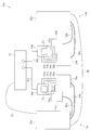
- Example 1 It is a basic lineblock diagram of a measurement system.
- Example 1 It is a block diagram of a measurement system.
- Example 1 It is a timing chart figure when measuring an electronic component.
- Example 1 A method of measuring characteristics of an electronic component of Example 1 will be described with reference to FIGS.
- FIG. 1 is a basic configuration diagram of a measurement system 10 that measures the characteristics of wireless communication modules 2a, 2b,..., 2x, which are electronic components on which an IC is mounted, using an RF tester 12 that is a single measuring instrument. . As shown in FIG. 1, a plurality of sub measurement systems 13 a, 13 b,..., 13 x are connected to one measuring device (RF tester) 12.
- RF tester measuring device
- Sub measurement systems 13a, 13b,..., 13x have the same configuration, and jigs on which electronic components 2a, 2b,..., 2x (wireless communication modules A, B,. , 14x (stages A, B,..., X) and the electronic components 2a, 2b,..., 2x mounted on the jigs 14a, 14b,.
- Control devices 20a, 20b,..., 20x module control personal computers A, B,..., X).
- the jigs 14a, 14b, ..., 14x (stages A, B, ..., X) of the sub measurement systems 13a, 13b, ..., 13x and the control devices 20a, 20b, ..., 20x are connected to the measuring instrument 12, respectively. Has been.
- the electronic component characteristic measuring method while the second process of measuring the characteristic of the electronic component mounted on the jig of a certain sub-measurement system is performed by the measuring instrument 12, another measurement system is used. For (a) the first process that activates the electronic component mounted on the jig to make it measurable and (b) the electronic component that has been measured by the measuring instrument 12 (second process), After writing data based on the measurement result obtained by the second process, the third process for stopping the activation of the electronic component, or (c) the fourth process for replacing the electronic component mounted on the jig I do.
- the operating rate of the measuring device can be increased by reducing or eliminating the waiting time.
- the operating rate of the measuring device can be increased.
- FIG. 2 is a configuration diagram of a measurement system 10a including two sub measurement systems 13a and 13b.
- the sub measurement systems 13a and 13b include jigs 14a and 14b (stages A and B) on which electronic components 2a and 2b (wireless communication modules A and B) are mounted, and a jig 14a. , 14b, control circuit boards 22a, 22b, power supplies 28a, 28b, and control devices 20a, 20b (module control personal computers A, B) for controlling the start, stop, and operation of the electronic components 2a, 2b.
- jigs 14a and 14b stages A and B
- control circuit boards 22a, 22b power supplies 28a, 28b
- control devices 20a, 20b module control personal computers A, B
- the jigs 14a and 14b are connected to the measuring instrument 12 through the RF cables 30a and 30b, and are connected to the control circuit boards 22a and 22b through the flat cables 31a and 31b.
- the jigs 14a and 14b and the control circuit boards 22a and 22b are connected to power supplies 28a and 28b via power cables 36a to 39a and 36b to 39b, respectively, and power is supplied from the power supplies 28a and 28b.
- the control devices 20a and 20b are connected to the control circuit boards 22a and 22b via the UART cables 32a and 32b, and are connected to the power supplies 28a and 28b via the GPIB cables 34a and 34b.
- the control devices 20a and 20b control operations of the control circuit boards 22a and 22b and the power supplies 28a and 28b.
- the control devices 20a and 20b of the sub measurement systems 13a and 13b are connected to each other by a LAN cable 35. Only the control device 20a of one sub measurement system 13a is connected to the measuring instrument 12 via the USB cable 33.
- the control device 20a of the one sub-measurement system 13a controls the overall measurement system 10a. That is, the control device 20a of one of the sub-measurement systems 13a supervises control for performing the first to fourth processes on the electronic components 2a and 2b mounted on the jigs 14a and 14b of the respective sub-measurement 13a and 13b systems. .
- the control device 20a of one sub measurement system 13a can grasp the measurement status of all the sub measurement systems 13a and 13b and optimize the measurement state, the measurement time can be shortened or another sub measurement system can be used.
- the wiring for connecting the control device 20b of the system 13b and the measuring device 20 can be eliminated.
- the measuring instrument 12 is always in an ON state that allows measurement.
- the first process 60a is performed on the electronic component (module A) mounted on the jig of one of the sub measurement systems.
- the second process 62b is performed on the electronic component (module B) mounted on the other sub-measurement system jig.
- the second process 62a is performed on the electronic component (module A) mounted on the jig of one of the sub measurement systems.
- the third process 64b is performed on the electronic component (module B) mounted on the other sub measurement system jig, and then the electronic component mounted on the other sub measurement system jig is mounted.
- a fourth process 68b to be replaced is performed, and then a first process 60b is performed on the electronic component (module B) newly mounted on the jig of the other sub measurement system.
- the second process 62b is performed on the electronic component (module B) mounted on the jig of the other sub measurement system.
- the third process 64a is performed on the electronic component (module A) mounted on the jig of one sub measurement system, and then the electronic component mounted on the jig of one sub measurement system is A fourth process 68a to be replaced is performed, and then a first process 60a is performed on the electronic component (module A) newly mounted on the jig of one of the sub measurement systems.
- control device 20a When the electronic component to be measured is a wireless communication module, the control device 20a operates as follows.
- the power supplies 28a and 28b are turned on to activate the wireless communication module mounted on the jigs 14a and 14b, and the data (Config file) to be read when the wireless communication module is activated, Read out from the memory of the wireless communication module mounted on the jigs 14a and 14b, and establish communication between the wireless communication module mounted on the jigs 14a and 14b and the control circuit boards 22a and 22b. Control is performed so as to perform an initial setting for enabling measurement of the wireless communication module mounted on the.
- control signals are transmitted from the control circuit boards 22a and 22b, the wireless communication modules mounted on the jigs 14a and 14b are operated, and transmission at a radio frequency is performed using the measuring instrument 12. Control to measure electrical characteristics such as reception.
- the third processing 64a and 64b data is processed based on the result of measuring the characteristics in the second processing 62a and 62b, and data (such as pass / fail judgment data) that can be used in subsequent processes is calculated. And data for identifying the wireless communication module (MAC address) are written in a memory in the wireless communication module mounted on the jigs 14a and 14b, and then the wireless communication module mounted on the jigs 14a and 14b Processing for terminating communication with the control circuit boards 22a and 22b is performed, and then control is performed to stop the power supply from the power supplies 28a and 28b to the wireless communication modules mounted on the jigs 14a and 14b.
- MAC address identifying the wireless communication module
- the pass / fail judgment data in the memory is read, and only non-defective products are taped.
- the first process can be performed on the electronic component that performs the RF measurement (second process) after the characteristic measurement process.
- the time required for the first processing 60a, 60b is t1
- the time required for the second processing 62a, 62b is t2
- the time required for the third processing 64a, 64b is t3
- the time required for the fourth processing 68a, 68b is t4 t2 ⁇ t1 + t3 + t4 If the above condition is satisfied, the operation rate of the measuring device 12 can be made 100% by alternately measuring the two sub-measuring systems 13a and 13b using one measuring device 12.
- n ⁇ t2 ⁇ t1 + t3 + t4 Assuming that the smallest positive integer satisfying n is n, and the number of sub measurement systems is (1 + n) or more, the measurement rate is 100% by measuring each sub measurement system using one measurement device. Can be.
- ⁇ Summary> As described above, while measuring the characteristics of an electronic component mounted on a jig of a certain sub-measurement system, processing is performed by the other sub-measurement system before and after the measurement.
- the measurement waiting time can be shortened or eliminated, and the operating time of the measuring device can be increased and the operating rate of the measuring device can be increased.
- the operating rate of the measuring instrument is increased, labor costs and capital investment can be suppressed, and the cost required for measuring the characteristics of electronic components can be reduced.
Landscapes
- Engineering & Computer Science (AREA)
- Computer Hardware Design (AREA)
- Microelectronics & Electronic Packaging (AREA)
- General Engineering & Computer Science (AREA)
- Physics & Mathematics (AREA)
- General Physics & Mathematics (AREA)
- Testing Of Individual Semiconductor Devices (AREA)
- Tests Of Electronic Circuits (AREA)
Abstract
測定器の稼働率を高めることができる電子部品の特性測定方法を提供する。 ICが搭載された電子部品の特性を、一つの測定器を用いて測定する。(a)電子部品を起動させて測定可能な状態にする第1の処理60a,60bと、(b)測定可能な状態となっている電子部品の特性を、測定器を用いて測定する第2の処理62a,62bと、(c)第2の処理62a,62bにより得られた測定結果に基づいて電子部品にデータを書き込んだ後に、電子部品の起動を停止させる第3の処理64a,64bとを順に行う。第2の処理62a,62bを行う特性測定工程中に、その後に第2の処理62a,62bを行う電子部品について第1の処理60a,60bを行う。
Description
本発明は、電子部品の特性測定方法に関し、詳しくは、ICが搭載された電子部品の特性を測定する方法に関する。
ICチップなどの電子部品は、電子部品にテスト信号を入力して動作させ、その応答信号によって特性が測定されている。
例えば特許文献1には、電子部品を、複数のテスタ(測定器)を用いて測定する方法が開示されている。この測定方法では、複数のテスターを用い、ある測定項目用のテスターで電子部品の特性を測定した後、電子部品を搬送し、別の測定項目用の別のテスターで電子部品の特性を測定する。
特許文献1のように複数のテスターを用いて測定する場合、コンデンサやフィルタなどの単一の機能のみを備えた部品であれば問題はないが、無線通信モジュールなどのように複数の測定項目があり、さらにモジュールを起動させるためにある程度の時間が必要となる電子部品では、テスターで測定するたびに、電子部品を立ち上げ(起動)するための工程と時間が必要になる。
また、無線通信モジュールなどでは、測定終了後に、測定結果などのデータをモジュール内のメモリに書き込む立ち下げのための工程と時間が必要になる。
このような立ち上げ及び立ち下げ工程を、テスターに電子部品が搬送され接続されてから行うと、立ち上げ及び立ち下げの時間分だけテスターが測定待ちの状態になり、特性測定工程に要する時間が長くなるという問題がある。また、特性測定工程中に、立ち上げ及び立ち下げのためテスターが稼働していない時間があると、製品価格に転嫁する設備コストが増大する。無線通信モジュールなどの特性測定に用いるテスターは高価であるため、製造コストへの影響が大きい。
本発明は、かかる実情に鑑み、測定器の稼働率を高めることができる電子部品の特性測定方法を提供しようとするものである。
本発明は、上記課題を解決するために、以下のように構成した電子部品の特性測定方法を提供する。
電子部品の特性測定方法は、ICが搭載された電子部品について、(a)前記電子部品を起動させて測定可能な状態にする第1の処理と、(b)前記第1の処理により測定可能な状態となっている前記電子部品の特性を、測定器を用いて測定する第2の処理と、(c)前記第2の処理により得られた測定結果に基づいて前記電子部品にデータを書き込んだ後に、前記電子部品の起動を停止させる第3の処理とを順に行う。前記第1の処理により測定可能な状態となっている前記電子部品について前記第2の処理を行う特性測定工程中に、当該特性測定工程の後に前記第2の処理を行う特性測定前の前記電子部品について前記第1の処理を行う。
上記方法によれば、第2の処理を行う特性測定工程中に、その後に第2の処理を行う電子部品について第1の処理を行う。これにより、第2の処理の待ち時間を短縮し、あるいは無くして、測定器の稼働率を高めることができる。
好ましくは、前記特性測定工程中に、当該特性測定工程より前に前記第2の処理を行った前記電子部品について前記第3の処理を行う。
この場合、測定器は、ある電子部品について第3の処理が行われている間に、他の電子部品について第2の処理を行う。これにより、測定器の稼働率を高めることができる。
好ましくは、(a)前記電子部品が搭載される治具と、(b)前記治具に搭載された前記電子部品の起動及び停止と動作を制御する制御機器とを含む複数のサブ測定系を用いる。前記測定器に一つの前記サブ測定系の前記制御機器のみを接続し、当該サブ測定系の前記制御機器を、他の前記サブ測定系の前記制御機器に接続する。当該サブ測定系の前記制御機器を用いて、前記各サブ測定系の前記治具に搭載された前記電子部品について前記第1乃至第3の処理を行う制御を統括する。
この場合、一つのサブ測定系の制御機器が、すべてのサブ測定系の測定状況を把握して、測定状態を最適化できるため、測定時間を短縮したり、他のサブ測定系の制御機器と測定器とを接続する配線を無くしたりすることができる。
本発明によれば、測定器の稼働率を高めることができる。
以下、本発明の実施の形態について、図1~図3を参照しながら説明する。
<実施例1> 実施例1の電子部品の特性測定方法について、図1~図3を参照しながら説明する。
図1は、ICが搭載された電子部品である無線通信モジュール2a,2b,…,2xの特性を、一つの測定器であるRFテスター12を用いて測定する測定系10の基本構成図である。図1に示すように、一つの測定器(RFテスター)12に、複数のサブ測定系13a,13b,…,13xが接続されている。
サブ測定系13a,13b,…,13xは、同じ構成であり、それぞれ、測定対象となる電子部品2a,2b,…,2x(無線通信モジュールA,B,…,X)が搭載される治具14a,14b,…,14x(ステージA,B,…,X)と、治具14a,14b,…,14xに搭載された電子部品2a,2b,…,2xの起動及び停止と動作を制御する制御機器20a,20b,…,20x(モジュール制御用パソコンA,B,…,X)とを含む。サブ測定系13a,13b,…,13xの治具14a,14b,…,14x(ステージA,B,…,X)と制御機器20a,20b,…,20xとは、それぞれ、測定器12に接続されている。
実施例1の電子部品の特性測定方法は、あるサブ測定系の治具に搭載されている電子部品の特性を測定器12で測定する第2の処理を行っている間に、他の測定系について、(a)治具に搭載された電子部品を起動させて測定可能な状態にする第1の処理や、(b)測定器12による測定(第2の処理)が完了した電子部品に、第2の処理により得られた測定結果に基づいてデータを書き込んだ後に、その電子部品の起動を停止させる第3の処理や、(c)治具に搭載する電子部品を交換する第4の処理を行う。
これによって、測定器12が測定待ちの状態にある時間を短縮し、あるいは無くして、測定器12が実際に電子部品の特性の測定を行う稼働時間を長くすることができる。すなわち、ある電子部品について第2の処理が行われている間に、他の電子部品について第1の処理を行うことにより、次に第2の処理を行うときに第1の処理が完了するまで待機する待ち時間を短縮し、あるいは無くして、測定器の稼働率を高めることができる。また、測定器は、ある電子部品について第3及び第4の処理が行われている間に、他の電子部品について第2の処理を行うため、測定器の稼働率を高めることができる。
次に、サブ測定系が2つの場合の具体例について、図2及び3を参照しながら説明する。
図2は、2つのサブ測定系13a,13bを含む測定系10aの構成図である。図2に示すように、サブ測定系13a,13bは、それぞれ、電子部品2a,2b(無線通信モジュールA,B)が搭載される治具14a,14b(ステージA,B)と、治具14a,14bに搭載された電子部品2a,2bの起動及び停止と動作を制御するための制御回路基板22a,22bと、電源28a,28bと、制御機器20a,20b(モジュール制御用パソコンA,B)とを含む。
各治具14a,14bは、RFケーブル30a,30bを介して測定器12に接続され、フラットケーブル31a,31bを介して制御回路基板22a,22bに接続されている。治具14a,14bと制御回路基板22a,22bとは、それぞれ電源ケーブル36a~39a,36b~39bを介して電源28a,28bに接続され、電源28a,28bから電力が供給される。制御機器20a,20bは、UARTケーブル32a,32bを介して制御回路基板22a,22bに接続され、GPIBケーブル34a,34bを介して電源28a,28bに接続されている。制御機器20a,20bは、制御回路基板22a,22bと電源28a,28bの動作を制御する。
サブ測定系13a,13bの制御機器20a,20b同士は、LANケーブル35で互いに接続されている。測定器12には、一方のサブ測定系13aの制御機器20aのみが、USBケーブル33を介して接続されている。一方のサブ測定系13aの制御機器20aは、測定系10a全体の制御を統括する。すなわち、一方のサブ測定系13aの制御機器20aは、各サブ測定13a,13b系の治具14a,14bに搭載された電子部品2a,2bについて第1乃至第4の処理を行う制御を統括する。
この場合、一つのサブ測定系13aの制御機器20aが、すべてのサブ測定系13a,13bの測定状況を把握して、測定状態を最適化できるため、測定時間を短縮したり、他のサブ測定系13bの制御機器20bと測定器20とを接続する配線を無くしたりすることができる。
次に、測定系10aを用いて電子部品の特性を測定するときの動作について、図3のタイミングチャートを参照しながら説明する。
図3(a)に示すように、測定器12は、常に測定可能なON状態である。
区間51において、一方のサブ測定系の治具に搭載された電子部品(モジュールA)について第1の処理60aを行う。また、この区間51において、他方のサブ測定系の治具に搭載された電子部品(モジュールB)について第2の処理62bを行う。
次の区間52において、一方のサブ測定系の治具に搭載された電子部品(モジュールA)について第2の処理62aを行う。また、この区間52において、他方のサブ測定系の治具に搭載された電子部品(モジュールB)について第3の処理64bを行い、次いで他方のサブ測定系の治具に搭載される電子部品を交換する第4の処理68bを行い、次いで、他方のサブ測定系の治具に新たに搭載された電子部品(モジュールB)について第1の処理60bを行う。
次の区間53において、他方のサブ測定系の治具に搭載された電子部品(モジュールB)について第2の処理62bを行う。また、この区間53において、一方のサブ測定系の治具に搭載された電子部品(モジュールA)について第3の処理64aを行い、次いで一方のサブ測定系の治具に搭載される電子部品を交換する第4の処理68aを行い、次いで、一方のサブ測定系の治具に新たに搭載された電子部品(モジュールA)について第1の処理60aを行う。
以下同様に、区間54,55,…において、2つのサブ測定系については、(a)第2の処理62a,62bと、(b)第3の処理64a,64b、第4の処理及68a,68b及び第1の処理60a,60bとを、交互に行う。
測定対象となる電子部品が無線通信モジュールの場合、制御機器20aは、次のように動作する。
第1の処理60a,60bにおいて、電源28a,28bを投入して、治具14a,14bに搭載された無線通信モジュールを起動させ、無線通信モジュールの起動時に読み出されるべきデータ(Configファイル)を、治具14a,14bに搭載された無線通信モジュールのメモリから読み出して、治具14a,14bに搭載された無線通信モジュールと制御回路基板22a,22bとの通信を確立するなど、治具14a,14bに搭載された無線通信モジュールの測定を可能にするための初期設定を行うように制御する。
第2の処理62a,62bにおいて、制御回路基板22a,22bから制御信号を送出して、治具14a,14bに搭載された無線通信モジュールを動作させ、測定器12を用いて、無線周波数における送信、受信などの電気的特性を測定するように制御する。
第3の処理64a,64bにおいて、第2の処理62a,62bで特性を測定した結果に基づいてデータを処理し、その後の工程で利用できるデータ(良否判定データなど)を算出し、算出したデータと、無線通信モジュールを識別するためのデータ(MACアドレス)を、治具14a,14bに搭載された無線通信モジュール内のメモリに書き込み、次いで、治具14a,14bに搭載された無線通信モジュールと制御回路基板22a,22bとの通信の終了処理を行い、次いで、治具14a,14bに搭載された無線通信モジュールへの電源28a,28bからの電力供給を停止するように制御する。
無線通信モジュールは、特性測定後のテーピング(梱包)工程において、メモリ内の良否判定データが読み取られ、良品のみがテーピングされる。
無線通信モジュールは、RF測定を行う第2の処理に要する時間が十分に長いため、一方のサブ測定系のRF測定(第2の処理)を行う特性測定工程中に、他方のサブ測定系において、当該特性測定工程の後にRF測定(第2の処理)を行う電子部品について第1の処理を行うことができる。
第1の処理60a,60bに要する時間をt1、第2の処理62a,62bに要する時間をt2、第3の処理64a,64bに要する時間をt3、第4の処理68a,68bに要する時間をt4とすると、
t2≧t1+t3+t4
を満たせば、1つの測定器12を用いて2つのサブ測定系13a,13bについて交互に測定することにより、測定器12の稼働率を100%にすることができる。
t2≧t1+t3+t4
を満たせば、1つの測定器12を用いて2つのサブ測定系13a,13bについて交互に測定することにより、測定器12の稼働率を100%にすることができる。
一般には、
n×t2≧t1+t3+t4
を満たす最小の正の整数をnとすると、サブ測定系の数を(1+n)以上にすると、1つの測定器を用いて各サブ測定系を測定することにより、測定器の稼働率を100%にすることができる。
n×t2≧t1+t3+t4
を満たす最小の正の整数をnとすると、サブ測定系の数を(1+n)以上にすると、1つの測定器を用いて各サブ測定系を測定することにより、測定器の稼働率を100%にすることができる。
<まとめ> 以上に説明したように、あるサブ測定系の治具に搭載された電子部品について特性を測定している間に、他のサブ測定系について測定前後の処理を行うことにより、測定器の測定待ち時間を短縮し、あるいは無くして、測定器の稼働時間を長くし、測定器の稼働率を高めることができる。測定器の稼働率を高めると、労務費や設備投資を抑制することができ、電子部品の特性測定に要するコストを低減することができる。
なお、本発明は、上記実施の形態に限定されるものではなく、種々変更を加えて実施することが可能である。
2a,2b,…,2x 電子部品
10,10a 測定系
12 測定器
13a,13b,…,13x サブ測定系
14a,14b,…,14x 治具
20a,20b,…,20x 制御機器
22a,22b 制御回路基板
28a,28b 電源
51~55 区間
60a,60b 第1の処理
62a,62b 第2の処理
64a,64b 第3の処理
68a,68b 第4の処理
10,10a 測定系
12 測定器
13a,13b,…,13x サブ測定系
14a,14b,…,14x 治具
20a,20b,…,20x 制御機器
22a,22b 制御回路基板
28a,28b 電源
51~55 区間
60a,60b 第1の処理
62a,62b 第2の処理
64a,64b 第3の処理
68a,68b 第4の処理
Claims (3)
- ICが搭載された電子部品について、
前記電子部品を起動させて測定可能な状態にする第1の処理と、
前記第1の処理により測定可能な状態となっている前記電子部品の特性を、測定器を用いて測定する第2の処理と、
前記第2の処理により得られた測定結果に基づいて前記電子部品にデータを書き込んだ後に、前記電子部品の起動を停止させる第3の処理と、
を順に行う電子部品の特性測定方法において、
前記第1の処理により測定可能な状態となっている前記電子部品について前記第2の処理を行う特性測定工程中に、当該特性測定工程の後に前記第2の処理を行う特性測定前の前記電子部品について前記第1の処理を行うことを特徴とする、電子部品の特性測定方法。 - 前記特性測定工程中に、
当該特性測定工程より前に前記第2の処理を行った前記電子部品について前記第3の処理を行うことを特徴とする、請求項1に記載の電子部品の特性測定方法。 - 前記電子部品が搭載される治具と、
前記治具に搭載された前記電子部品の起動及び停止と動作を制御する制御機器と、
を含む複数のサブ測定系を用い、
前記測定器に一つの前記サブ測定系の前記制御機器のみを接続し、当該サブ測定系の前記制御機器を、他の前記サブ測定系の前記制御機器に接続し、
当該サブ測定系の前記制御機器を用いて、前記各サブ測定系の前記治具に搭載された前記電子部品について前記第1乃至第3の処理を行う制御を統括することを特徴とする、請求項1又は2に記載された電子部品の特性測定方法。
Priority Applications (2)
| Application Number | Priority Date | Filing Date | Title |
|---|---|---|---|
| JP2013520548A JP5673819B2 (ja) | 2011-06-16 | 2012-06-11 | 電子部品の特性測定方法 |
| CN201280029167.XA CN103620428B (zh) | 2011-06-16 | 2012-06-11 | 电子元器件的特性测量方法 |
Applications Claiming Priority (2)
| Application Number | Priority Date | Filing Date | Title |
|---|---|---|---|
| JP2011-133904 | 2011-06-16 | ||
| JP2011133904 | 2011-06-16 |
Publications (1)
| Publication Number | Publication Date |
|---|---|
| WO2012173093A1 true WO2012173093A1 (ja) | 2012-12-20 |
Family
ID=47357080
Family Applications (1)
| Application Number | Title | Priority Date | Filing Date |
|---|---|---|---|
| PCT/JP2012/064924 Ceased WO2012173093A1 (ja) | 2011-06-16 | 2012-06-11 | 電子部品の特性測定方法 |
Country Status (3)
| Country | Link |
|---|---|
| JP (1) | JP5673819B2 (ja) |
| CN (1) | CN103620428B (ja) |
| WO (1) | WO2012173093A1 (ja) |
Citations (4)
| Publication number | Priority date | Publication date | Assignee | Title |
|---|---|---|---|---|
| JPS61153574A (ja) * | 1984-12-26 | 1986-07-12 | Nec Corp | 半導体装置の試験装置 |
| JPH10104308A (ja) * | 1996-09-27 | 1998-04-24 | Ando Electric Co Ltd | Ic試験装置 |
| JP2000208567A (ja) * | 1999-01-18 | 2000-07-28 | Nec Corp | 半導体集積回路及びそのテスト方法 |
| WO2008072639A1 (ja) * | 2006-12-13 | 2008-06-19 | Advantest Corporation | 試験装置、試験方法、及び接続部 |
Family Cites Families (1)
| Publication number | Priority date | Publication date | Assignee | Title |
|---|---|---|---|---|
| MY140086A (en) * | 2004-07-23 | 2009-11-30 | Advantest Corp | Electronic device test apparatus and method of configuring electronic device test apparatus |
-
2012
- 2012-06-11 WO PCT/JP2012/064924 patent/WO2012173093A1/ja not_active Ceased
- 2012-06-11 CN CN201280029167.XA patent/CN103620428B/zh not_active Expired - Fee Related
- 2012-06-11 JP JP2013520548A patent/JP5673819B2/ja not_active Expired - Fee Related
Patent Citations (4)
| Publication number | Priority date | Publication date | Assignee | Title |
|---|---|---|---|---|
| JPS61153574A (ja) * | 1984-12-26 | 1986-07-12 | Nec Corp | 半導体装置の試験装置 |
| JPH10104308A (ja) * | 1996-09-27 | 1998-04-24 | Ando Electric Co Ltd | Ic試験装置 |
| JP2000208567A (ja) * | 1999-01-18 | 2000-07-28 | Nec Corp | 半導体集積回路及びそのテスト方法 |
| WO2008072639A1 (ja) * | 2006-12-13 | 2008-06-19 | Advantest Corporation | 試験装置、試験方法、及び接続部 |
Also Published As
| Publication number | Publication date |
|---|---|
| JPWO2012173093A1 (ja) | 2015-02-23 |
| JP5673819B2 (ja) | 2015-02-18 |
| CN103620428B (zh) | 2015-12-09 |
| CN103620428A (zh) | 2014-03-05 |
Similar Documents
| Publication | Publication Date | Title |
|---|---|---|
| US20210341531A1 (en) | Method for continuous tester operation during long soak time testing | |
| CN107462821B (zh) | 晶圆测试机台的远端监控方法及系统 | |
| CN217766725U (zh) | 芯片测试系统及芯片测试装置 | |
| CN107450008A (zh) | 芯片测试系统 | |
| CN100420956C (zh) | 多个测试端口的快速校准方法 | |
| JP5673819B2 (ja) | 電子部品の特性測定方法 | |
| CN102759648A (zh) | 电源板测试方法和系统 | |
| CN116299023A (zh) | 一种电源测试方法、装置、设备及存储介质 | |
| CN102890232A (zh) | 平行测试方法 | |
| CN103760486A (zh) | 电路板上特殊芯片的功能测试装置 | |
| KR20120066158A (ko) | 테스트 방법 및 이를 수행하기 위한 장치 | |
| CN1856712A (zh) | 用于优化电子电路的测试和配置吞吐量的系统和方法 | |
| CN104516797A (zh) | 主板管理控制器测试系统和方法 | |
| CN203658835U (zh) | 一种用于多种航天型号电源控制器的测试系统 | |
| CN204374339U (zh) | 一种在线式老化测试装置 | |
| US20150192638A1 (en) | Semiconductor test device and method of operating the same | |
| JP5086983B2 (ja) | プローブ装置、処理装置及びウェハプローブテストの処理方法 | |
| US20140380110A1 (en) | Test apparatus and operating method thereof | |
| JPWO2007132577A1 (ja) | プラットフォームボード及び生産管理方法 | |
| TWI665457B (zh) | 量測系統及其量測方法 | |
| US10386405B2 (en) | Method for continuous tester operation during multiple stage temperature testing | |
| US9638740B2 (en) | Test system with rotational test arms for testing semiconductor components | |
| CN110161977B (zh) | 测量系统及其测量方法 | |
| KR100903681B1 (ko) | 전원단 회로, 전원단 회로 설계장치 및 방법 | |
| US20230420068A1 (en) | Semiconductor test apparatus capable of inducing reduction of power consumption |
Legal Events
| Date | Code | Title | Description |
|---|---|---|---|
| 121 | Ep: the epo has been informed by wipo that ep was designated in this application |
Ref document number: 12800084 Country of ref document: EP Kind code of ref document: A1 |
|
| ENP | Entry into the national phase |
Ref document number: 2013520548 Country of ref document: JP Kind code of ref document: A |
|
| NENP | Non-entry into the national phase |
Ref country code: DE |
|
| 122 | Ep: pct application non-entry in european phase |
Ref document number: 12800084 Country of ref document: EP Kind code of ref document: A1 |