WO2012173037A1 - 表示装置 - Google Patents
表示装置 Download PDFInfo
- Publication number
- WO2012173037A1 WO2012173037A1 PCT/JP2012/064666 JP2012064666W WO2012173037A1 WO 2012173037 A1 WO2012173037 A1 WO 2012173037A1 JP 2012064666 W JP2012064666 W JP 2012064666W WO 2012173037 A1 WO2012173037 A1 WO 2012173037A1
- Authority
- WO
- WIPO (PCT)
- Prior art keywords
- light
- diffusion layer
- display device
- light diffusion
- blue
- Prior art date
- Legal status (The legal status is an assumption and is not a legal conclusion. Google has not performed a legal analysis and makes no representation as to the accuracy of the status listed.)
- Ceased
Links
Images








Classifications
-
- G—PHYSICS
- G02—OPTICS
- G02B—OPTICAL ELEMENTS, SYSTEMS OR APPARATUS
- G02B26/00—Optical devices or arrangements for the control of light using movable or deformable optical elements
- G02B26/02—Optical devices or arrangements for the control of light using movable or deformable optical elements for controlling the intensity of light
-
- G—PHYSICS
- G02—OPTICS
- G02B—OPTICAL ELEMENTS, SYSTEMS OR APPARATUS
- G02B5/00—Optical elements other than lenses
- G02B5/02—Diffusing elements; Afocal elements
- G02B5/0205—Diffusing elements; Afocal elements characterised by the diffusing properties
- G02B5/0236—Diffusing elements; Afocal elements characterised by the diffusing properties the diffusion taking place within the volume of the element
- G02B5/0242—Diffusing elements; Afocal elements characterised by the diffusing properties the diffusion taking place within the volume of the element by means of dispersed particles
-
- G—PHYSICS
- G02—OPTICS
- G02B—OPTICAL ELEMENTS, SYSTEMS OR APPARATUS
- G02B5/00—Optical elements other than lenses
- G02B5/02—Diffusing elements; Afocal elements
- G02B5/0273—Diffusing elements; Afocal elements characterized by the use
- G02B5/0278—Diffusing elements; Afocal elements characterized by the use used in transmission
-
- G—PHYSICS
- G02—OPTICS
- G02B—OPTICAL ELEMENTS, SYSTEMS OR APPARATUS
- G02B5/00—Optical elements other than lenses
- G02B5/20—Filters
- G02B5/201—Filters in the form of arrays
-
- G—PHYSICS
- G02—OPTICS
- G02F—OPTICAL DEVICES OR ARRANGEMENTS FOR THE CONTROL OF LIGHT BY MODIFICATION OF THE OPTICAL PROPERTIES OF THE MEDIA OF THE ELEMENTS INVOLVED THEREIN; NON-LINEAR OPTICS; FREQUENCY-CHANGING OF LIGHT; OPTICAL LOGIC ELEMENTS; OPTICAL ANALOGUE/DIGITAL CONVERTERS
- G02F1/00—Devices or arrangements for the control of the intensity, colour, phase, polarisation or direction of light arriving from an independent light source, e.g. switching, gating or modulating; Non-linear optics
- G02F1/01—Devices or arrangements for the control of the intensity, colour, phase, polarisation or direction of light arriving from an independent light source, e.g. switching, gating or modulating; Non-linear optics for the control of the intensity, phase, polarisation or colour
- G02F1/13—Devices or arrangements for the control of the intensity, colour, phase, polarisation or direction of light arriving from an independent light source, e.g. switching, gating or modulating; Non-linear optics for the control of the intensity, phase, polarisation or colour based on liquid crystals, e.g. single liquid crystal display cells
- G02F1/133—Constructional arrangements; Operation of liquid crystal cells; Circuit arrangements
- G02F1/1333—Constructional arrangements; Manufacturing methods
- G02F1/1335—Structural association of cells with optical devices, e.g. polarisers or reflectors
- G02F1/133504—Diffusing, scattering, diffracting elements
-
- G—PHYSICS
- G02—OPTICS
- G02F—OPTICAL DEVICES OR ARRANGEMENTS FOR THE CONTROL OF LIGHT BY MODIFICATION OF THE OPTICAL PROPERTIES OF THE MEDIA OF THE ELEMENTS INVOLVED THEREIN; NON-LINEAR OPTICS; FREQUENCY-CHANGING OF LIGHT; OPTICAL LOGIC ELEMENTS; OPTICAL ANALOGUE/DIGITAL CONVERTERS
- G02F1/00—Devices or arrangements for the control of the intensity, colour, phase, polarisation or direction of light arriving from an independent light source, e.g. switching, gating or modulating; Non-linear optics
- G02F1/01—Devices or arrangements for the control of the intensity, colour, phase, polarisation or direction of light arriving from an independent light source, e.g. switching, gating or modulating; Non-linear optics for the control of the intensity, phase, polarisation or colour
- G02F1/13—Devices or arrangements for the control of the intensity, colour, phase, polarisation or direction of light arriving from an independent light source, e.g. switching, gating or modulating; Non-linear optics for the control of the intensity, phase, polarisation or colour based on liquid crystals, e.g. single liquid crystal display cells
- G02F1/133—Constructional arrangements; Operation of liquid crystal cells; Circuit arrangements
- G02F1/1333—Constructional arrangements; Manufacturing methods
- G02F1/1335—Structural association of cells with optical devices, e.g. polarisers or reflectors
- G02F1/1336—Illuminating devices
- G02F1/133617—Illumination with ultraviolet light; Luminescent elements or materials associated to the cell
-
- G—PHYSICS
- G02—OPTICS
- G02F—OPTICAL DEVICES OR ARRANGEMENTS FOR THE CONTROL OF LIGHT BY MODIFICATION OF THE OPTICAL PROPERTIES OF THE MEDIA OF THE ELEMENTS INVOLVED THEREIN; NON-LINEAR OPTICS; FREQUENCY-CHANGING OF LIGHT; OPTICAL LOGIC ELEMENTS; OPTICAL ANALOGUE/DIGITAL CONVERTERS
- G02F1/00—Devices or arrangements for the control of the intensity, colour, phase, polarisation or direction of light arriving from an independent light source, e.g. switching, gating or modulating; Non-linear optics
- G02F1/01—Devices or arrangements for the control of the intensity, colour, phase, polarisation or direction of light arriving from an independent light source, e.g. switching, gating or modulating; Non-linear optics for the control of the intensity, phase, polarisation or colour
- G02F1/13—Devices or arrangements for the control of the intensity, colour, phase, polarisation or direction of light arriving from an independent light source, e.g. switching, gating or modulating; Non-linear optics for the control of the intensity, phase, polarisation or colour based on liquid crystals, e.g. single liquid crystal display cells
- G02F1/133—Constructional arrangements; Operation of liquid crystal cells; Circuit arrangements
- G02F1/1333—Constructional arrangements; Manufacturing methods
- G02F1/1335—Structural association of cells with optical devices, e.g. polarisers or reflectors
- G02F1/133509—Filters, e.g. light shielding masks
- G02F1/133514—Colour filters
Definitions
- the present invention relates to a display device, and more particularly, to a display device using an illumination device that emits blue light in order to improve light utilization efficiency.
- liquid crystal display devices have been widely used for information devices such as notebook personal computers, mobile phones, electronic notebooks, or camera-integrated VTRs equipped with a liquid crystal monitor, taking advantage of their thinness and low power consumption. ing.
- a general liquid crystal display device includes an illuminating device (backlight) that emits white light. Red light, green light, and blue light are applied to regions corresponding to red pixels, green pixels, and blue pixels of the liquid crystal panel. A color filter that selectively transmits light is provided.
- Patent Documents 1 and 2 propose a liquid crystal display device using an illumination device that emits blue light as a backlight.
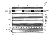
- FIG. 16 shows a liquid crystal display device 900 disclosed in Patent Document 2.
- FIG. 16 is a cross-sectional view schematically showing the liquid crystal display device 900.
- the liquid crystal display device 900 includes a backlight 910, a back side polarizing plate 901, a liquid crystal panel 920, an observer side polarizing plate 902, a color filter 903, and a light scattering film 904, as shown in FIG. These are provided in this order from the back side.
- the backlight 910 includes a light guide plate 914 and a blue light emitting diode (blue LED) 911 disposed on the end face of the light guide plate 914.
- a reflective sheet 915 is provided on the back side of the light guide plate 914, and a reflective plate 916 is provided so as to surround the blue LED 911.
- a first diffusion sheet 917, a prism sheet 918 and a second diffusion sheet 919 are provided on the front side of the light guide plate 914.
- the liquid crystal panel 920 includes a pair of substrates 921 and 922 and a liquid crystal layer 923 provided between the substrates 921 and 922. Electrodes 924a and 924b are provided on the liquid crystal layer 923 side of the pair of substrates 921 and 922, respectively. In addition, alignment films 925a and 925b are provided on the electrodes 924a and 924b so as to be in contact with the liquid crystal layer 923, respectively.
- the color filter 903 includes a red color developing layer 903R provided in a region corresponding to the red pixel R, a green color developing layer 903G provided in a region corresponding to the green pixel G, and a blue transmission provided in a region corresponding to the blue pixel B.
- a layer 903B and a black matrix 903BM provided between the pixels are included.
- the red coloring layer 903R is formed of a phosphor material that emits red light when excited by blue light.
- the green coloring layer 903G is formed of a phosphor material that emits green light when excited by blue light.
- the blue transmissive layer 903B is formed of a material that transmits at least blue light.
- the color filter 903 of the liquid crystal display device 900 is greatly different from a conventional general color filter.
- Blue light emitted from the backlight 910 is incident on the liquid crystal panel 920 via the back side polarizing plate 901.
- the liquid crystal panel 920 controls the amount of blue light that modulates blue light and transmits through the observer-side polarizing plate 902 for each pixel.
- the blue light transmitted through the observer side polarizing plate 902 is incident on the color filter 903.
- the blue light incident on the region corresponding to the red pixel R of the color filter 903 excites the phosphor material of the red coloring layer 903R, and thereby the red coloring layer 903R emits red light.
- the blue light incident on the area corresponding to the green pixel G of the color filter 903 excites the phosphor material of the green color developing layer 903G, whereby the green color developing layer 903G emits green light.
- the blue light that has entered the region corresponding to the blue pixel B of the color filter 903 passes through the blue transmission layer 903B. Red light, green light, and blue light emitted from the color filter 903 are scattered by the light scattering film 904.
- the backlight 910 that emits blue light, the red coloring layer 903R that emits red light when excited by the blue light, and the green coloring layer 903G that emits green light when excited by the blue light can be performed.
- the light use efficiency is high as compared with the configuration in which the illumination device that emits white light and the color filter are combined, which is employed in a conventional general liquid crystal display device.
- the red coloring layer 903R and the green coloring layer 903G emit isotropically red light and green light, respectively.
- the blue transmission layer 903B simply transmits blue light with high directivity (that is, high parallelism). Therefore, the red light and green light emitted from the red coloring layer 903R and the green coloring layer 903G and the blue light transmitted through the blue transmission layer 903B have greatly different angular characteristics (intensity distribution).
- the light scattering film 904 is provided on the viewer side with respect to the color filter 903, the blue light transmitted through the blue transmission layer 903B is scattered by the light scattering film 904. Therefore, the difference in angle characteristics between red light, green light, and blue light can be reduced, and the difference in viewing angle characteristics between red pixel R, green pixel G, and blue pixel B can be reduced.
- a single (that is, a common) light scattering film 904 is provided for the red pixel R, the green pixel G, and the blue pixel B. It is difficult to make the angular characteristics of light, green light, and blue light substantially the same by the light scattering film 904 common to all color pixels. Therefore, it is actually difficult to align the viewing angle characteristics of the red pixel R, the green pixel G, and the blue pixel B.
- the present invention has been made in view of the above problems, and an object of the present invention is to provide a display device that has high light use efficiency and a sufficiently small difference in viewing angle characteristics between pixels that display primary colors. There is to do.
- a display device is a display device having a plurality of pixels including a red pixel, a green pixel, and a blue pixel, an illumination device that emits blue light, and a blue light emitted from the illumination device.
- An optical shutter array capable of controlling transmittance in each of the plurality of pixels, a red phosphor layer provided corresponding to the red pixel and emitting red light when excited by blue light, and corresponding to the green pixel
- a green phosphor layer that emits green light when excited by blue light
- a first light diffusion layer that is provided corresponding to the blue pixel and diffuses the blue light transmitted through the optical shutter array.
- the first light diffusion layer diffuses blue light by Mie scattering.
- the first light diffusion layer has a transparent material and particles dispersed in the transparent material, and the average particle size of the particles is 500 nm or less.
- the average particle diameter of the particles is 200 nm or less.
- the particles are made of a material containing a metal element.
- the particles are formed from a metal oxide.
- the transparent material has a refractive index of 1.48 or more and 1.52 or less
- the first light diffusion layer contains 5% by mass or more and 30% by mass or less of the particles.
- the haze value of the first light diffusion layer is 93% or more, and the diffusion transmittance of the first light diffusion layer is 40% or more.
- a display device is provided corresponding to the red pixel, and corresponds to the green pixel, a second light diffusion layer that diffuses red light emitted from the red phosphor layer, and the green pixel. And a third light diffusion layer for diffusing green light emitted from the green phosphor layer.
- the first light diffusion layer, the second light diffusion layer, and the third light diffusion layer are made of different materials.
- the first light diffusion layer, the second light diffusion layer, and the third light diffusion layer are formed of the same material, and the second light diffusion layer and the third light diffusion layer are formed.
- the thickness of the light diffusion layer is smaller than the thickness of the first light diffusion layer.
- the optical shutter array is a liquid crystal panel having a pair of substrates and a liquid crystal layer provided between the pair of substrates.
- the red phosphor layer and the green phosphor layer are disposed in the liquid crystal panel.
- the light diffusion portion including the first light diffusion layer has a light shielding layer provided in a corresponding region between the plurality of pixels.
- the blue light emitted from the illumination device is substantially parallel light.
- a display device with high light utilization efficiency and a sufficiently small difference in viewing angle characteristics between pixels displaying each primary color is provided.
- FIG. 4 is a diagram illustrating an example of a specific configuration of a first light diffusion layer 41 provided in the display device 100.
- FIG. FIGS. 5A to 5F are process cross-sectional views illustrating a process of forming the light diffusion portion 40 including the first light diffusion layer 41.
- FIG. 4 is a graph showing the angle characteristics of blue light bl transmitted through a sample 2 and the angle characteristics of red light rl and green light gl transmitted through a second light diffusion layer 42 and a third light diffusion layer 43, respectively.
- 4 is a graph showing the angle characteristics of blue light bl transmitted through a sample 1 and the angle characteristics of red light rl and green light gl transmitted through a second light diffusion layer 42 and a third light diffusion layer 43, respectively. It is a graph which shows the result of having performed the simulation using the average particle diameter, refractive index, density
- FIG. 6 is a cross-sectional view showing another example of the configuration of the first light diffusion layer 41.
- FIG. 6 is a cross-sectional view showing another example of the configuration of the light diffusing unit 40.
- FIG. (A) And (b) is sectional drawing which shows the example of the concrete structure of the illuminating device 10 which can radiate
- (A) And (b) is a figure which shows the example of the concrete structure of the MEMS shutter array 60 with which the display apparatus 200 is provided, and is a top view which shows typically the area
- 4 is a cross-sectional view illustrating an example of a preferable configuration of a light diffusing unit 40 included in the display device 300.
- FIG. 11 is a cross-sectional view schematically showing a liquid crystal display device 900 disclosed in Patent Document 2.
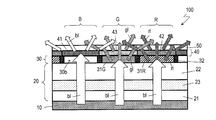
- FIG. 1 shows a display device 100 according to this embodiment.
- FIG. 1 is a cross-sectional view schematically showing the display device 100.
- the display device 100 includes a plurality of pixels including a red pixel R for displaying red, a green pixel G for displaying green, and a blue pixel B for displaying blue, as shown in FIG.
- the plurality of pixels are arranged in a matrix within the display area.
- the display device 100 includes the illumination device 10, the liquid crystal panel 20, a red phosphor layer 31 ⁇ / b> R and a green phosphor layer 31 ⁇ / b> G, and a first light diffusion layer 41.
- the illumination device (backlight) 10 emits blue light.
- the blue light emitted from the illumination device 10 is substantially parallel light.
- a specific configuration of the illumination device 10 that emits substantially parallel light will be described in detail later.
- the liquid crystal panel 20 is disposed on the observer side of the illumination device 10.
- the liquid crystal panel 20 can control the transmittance of the blue light emitted from the illumination device 10 in each of the plurality of pixels. That is, the liquid crystal panel 20 functions as an optical shutter array.
- the liquid crystal panel 20 includes a pair of substrates 21 and 22 and a liquid crystal layer 23 provided between the pair of substrates 21 and 22.
- liquid crystal panels for various display modes such as a TN (Twisted / Nematic) mode, a VA (Vertical / Alignment) mode, and an IPS (In-Plane / Switching) mode can be used.
- the liquid crystal panel 20 does not have a color filter.
- the substrate 21 on the back side of the pair of substrates 21 and 22 is typically an active matrix substrate (TFT) having a thin film transistor (TFT) and a pixel electrode (both not shown) provided in each of a plurality of pixels. Substrate).
- TFT active matrix substrate
- TFT thin film transistor
- pixel electrode both not shown
- the viewer-side substrate (counter substrate) 22 of the pair of substrates 21 and 22 has a counter electrode (not shown) facing the pixel electrode.
- many display mode liquid crystal panels 20 are used in combination with a pair of polarizing plates (not shown) that face each other with a liquid crystal layer 23 interposed therebetween.
- the pair of polarizing plates is provided outside the substrates 21 and 22.
- the red phosphor layer 31R and the green phosphor layer 31G are arranged on the viewer side of the liquid crystal panel 20.
- the red phosphor layer 31R is provided corresponding to the red pixel R and is excited by blue light to emit red light.
- the green phosphor layer 31G is provided corresponding to the green pixel G and is excited by blue light to emit green light.
- the material of the red phosphor layer 31R and the green phosphor layer 31G and various known phosphor materials that emit red light or green light when excited by blue light are used regardless of whether they are organic or inorganic. be able to.
- the phosphor material disclosed in Patent Document 2 can be suitably used.
- the portion where the red phosphor layer 31R and the green phosphor layer 31G are provided in the thickness direction of the display device 100 is also referred to as a color developing unit 30 in a comprehensive manner.
- the phosphor layer is not provided in the region 30b corresponding to the blue pixel B of the color developing portion 30.
- a transparent resin layer may be provided.
- the thickness of the color developing portion 30 is, for example, 10 ⁇ m to 30 ⁇ m.
- a light shielding layer 32 is provided in a region corresponding to a space between two adjacent pixels of the color developing unit 30. Since the red phosphor layer 31R and the green phosphor layer 31G emit light isotropically, the provision of such a light shielding layer 32 prevents light from leaking to other pixels. Can do. As a material of the light shielding layer 32, for example, a black resin can be used.
- the color forming section 30 may be provided on the observer-side polarizing plate of the pair of polarizing plates, or provided below (that is, between the observer-side polarizing plate and the counter substrate 22). It may be done. When the former arrangement is adopted, since the red phosphor layer 31R and the green phosphor layer 31G are located closer to the viewer than the latter arrangement, there is an advantage that the viewing angle characteristics are good.
- the first light diffusion layer 41 is provided corresponding to the blue pixel B, and diffuses the blue light transmitted through the liquid crystal panel 20 that is an optical shutter array.
- the first light diffusion layer 41 diffuses blue light by Mie scattering.
- Mie scattering is a kind of light scattering phenomenon caused by particles.
- the display device 100 further includes a second light diffusion layer 42 and a third light diffusion layer 43.
- the second light diffusion layer 42 is provided corresponding to the red pixel R, and diffuses the red light emitted from the red phosphor layer 31R.
- the third light diffusion layer 43 is provided corresponding to the green pixel G, and diffuses the green light emitted from the green phosphor layer 31G.
- the second light diffusion layer 42, the third light diffusion layer 43, and the first light diffusion layer 41 are formed of different materials.
- a portion where the first light diffusion layer 41, the second light diffusion layer 42, and the third light diffusion layer 43 are provided in the thickness direction of the display device 100 is collectively referred to as a light diffusion portion 40.
- the thickness of the light diffusion portion 40 is, for example, 5 ⁇ m to 30 ⁇ m.
- a transparent protective plate 50 is provided on the light diffusion portion 40.
- the protection plate 50 is a thin glass plate, for example.
- FIG. 2 shows how the display device 100 performs display.
- the blue light bl emitted from the illumination device 10 enters the liquid crystal panel 20.
- the liquid crystal panel 20 that is an optical shutter array controls the transmittance of the blue light bl for each pixel.
- the blue light bl transmitted through the liquid crystal panel 20 is incident on the color developing unit 30.
- a part of the blue light bl incident on the color forming part 30 excites the red phosphor layer 31R. Thereby, the red phosphor layer 31R emits red light rl. At this time, the red light rl is emitted isotropically.
- the other part of the blue light bl incident on the color forming unit 30 excites the green phosphor layer 31G. Thereby, the green phosphor layer 31G emits green light gl. At this time, the green light gl is emitted isotropically.
- Still another part of the blue light bl that has entered the color developing section 30 passes through the region 30b (no phosphor layer is provided) corresponding to the blue pixel B. At this time, the blue light bl remains substantially parallel light.
- the light from the coloring section 30 is diffused by the light diffusing section 40.
- the blue light bl that has passed through the region 30 b corresponding to the blue pixel B of the color forming unit 30 is diffused by the first light diffusion layer 41.
- the red light rl emitted from the red phosphor layer 31 ⁇ / b> R is diffused by the second light diffusion layer 42.
- the green light gl emitted from the green phosphor layer 31G is diffused by the third light diffusion layer 43.
- the illumination device 10 that emits the blue light bl, the red phosphor layer 31R that is excited by the blue light bl and emits the red light rl, and the green light gl that is excited by the blue light bl.
- the green phosphor layer 31G that emits light, color display can be performed. For this reason, the light use efficiency is high as compared with the configuration in which the illumination device that emits white light and the color filter are combined, which is employed in a conventional general liquid crystal display device.
- the light diffusion layer is separately provided for the blue pixel B, the red pixel R, and the green pixel G.
- the first light diffusion layer 41 is provided for the blue pixel B
- the second light diffusion layer 42 is provided for the red pixel R
- the third light diffusion is provided for the green pixel G.
- a layer 43 is provided. Therefore, the difference between the angle characteristics of the blue light bl and the angle characteristics of the red light rl and the green light gl can be made sufficiently small by the light diffusion unit 40.
- the first light diffusion layer 41 diffuses the blue light bl by Mie scattering. Therefore, the first light diffusion layer 41 is more isotropic than a light diffusion layer generally used as an optical element of a liquid crystal display device, that is, a light diffusion layer that diffuses light by geometric scattering. Light is diffused (scattered). Therefore, even if the blue light bl emitted from the illumination device 10 is substantially parallel light, the angle characteristics of the blue light bl and the angle characteristics of the red light rl and the green light gl are sufficiently close (for example, substantially the same). can do. Therefore, in the display device 100 of this embodiment, the difference in viewing angle characteristics among the red pixel R, the green pixel G, and the blue pixel B can be sufficiently reduced.
- FIG. 3 shows an example of a specific configuration of the first light diffusion layer 41.
- the first light diffusion layer 41 shown in FIG. 3 includes a matrix 41a formed from a transparent material and particles 41b dispersed in the matrix 41a.
- the transparent material that is the material of the matrix 41a is typically a resin material.
- the kind of resin material is not specifically limited, As a resin material, a thermoplastic resin and a thermosetting resin can be used suitably, for example.
- As a specific resin material for example, acrylic resin, polycarbonate, or polyester can be used.
- the refractive indices of acrylic resin, polycarbonate and polyester are 1.49, 1.59 and 1.6, respectively.
- the particle 41b is typically formed from a material containing a metal element, for example, a metal oxide.
- a metal element include titanium (Ti), zirconium (Zr), aluminum (Al), tin (Sn), and antimony (Sb).
- the metal oxide include TiO 2 , ZrO 2 , Al 2 O 3 , SnO 2 and Sb 2 O 3 are mentioned.
- the refractive indexes of TiO 2 , ZrO 2 , Al 2 O 3 , SnO 2 and Sb 2 O 3 are 2.71, 2.15, 1.63, 2.03 and 2.1, respectively.
- the average particle diameter of the particles 41b is preferably 500 nm or less, and more preferably 200 nm or less. However, from the viewpoint of sufficiently increasing the scattering intensity, the average particle diameter of the particles 41b is preferably 250 nm or more.
- dispersed structures can be mentioned.
- the haze value of the first light diffusion layer 41 is preferably 93% or more, and the diffusion transmittance of the first light diffusion layer 41 is 40%. % Or more is preferable.
- the second light diffusion layer 42 and the third light diffusion layer 43 also typically have a matrix formed of a transparent material and particles dispersed in the matrix. However, the light diffusion characteristics of the second light diffusion layer 42 and the third light diffusion layer 43 are different from the light diffusion characteristics of the first light diffusion layer 41.
- Each of the second light diffusion layer 42 and the third light diffusion layer 43 may be one that diffuses light by Mie scattering, or may diffuse light by geometric scattering. When light is diffused by geometric scattering, the average particle size of the particles is typically 10 ⁇ m or more.
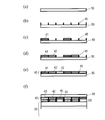
- 4A to 4F are process cross-sectional views illustrating the process of forming the light diffusion portion 40.
- a protective plate 50 is prepared.
- the thickness is, for example, about 0.3 mm to 1.0 mm.
- a wall-like structure 45 is formed on the protective plate 50.
- the wall-like structure 45 is provided so as to be positioned between the pixels, and functions as a light shielding layer.
- a material of the wall-like structure (light shielding layer) 45 a material used for a black matrix of a liquid crystal panel or a resin material having a light shielding property can be used.
- a first light diffusion layer 41 is formed.
- the first light diffusion layer 41 is formed by applying a diffusion layer material including a transparent material to be the matrix 41a and particles 41b to a region corresponding to the blue pixel B on the protection plate 50.
- the dispersion amount (concentration) of the particles 41b is adjusted so that the blue light bl can be suitably diffused.
- the second light diffusion layer 42 is formed. Specifically, the second light diffusion layer 42 is formed by applying a diffusion layer material including a transparent material and particles as a matrix to a region corresponding to the red pixel R on the protection plate 50. The dispersion amount (concentration) of the particles is adjusted so that the red light rl can be suitably diffused.
- a third light diffusion layer 43 is formed.
- the third light diffusion layer 43 is formed by applying a diffusion layer material including a transparent material and particles as a matrix to a region corresponding to the green pixel G on the protection plate 50.
- the dispersion amount (concentration) of the particles is adjusted so that the green light gl can be suitably diffused.
- the diffusion layer material for forming the first light diffusion layer 41, the second light diffusion layer 42, and the third light diffusion layer 43 can be applied by, for example, an inkjet method. Or it can also apply
- the light diffusing unit 40 (and the protective plate 50) is joined to the color developing unit 30 provided on the viewer side of the liquid crystal panel 20.
- the light diffusing unit 40 is joined to the coloring unit 30 using, for example, an ultraviolet curable resin or a thermosetting resin.
- the first light diffusing layer 41 using Mie scattering and the light diffusing layer using geometric scattering are actually manufactured (referred to as samples 1 and 2 respectively), and substantially parallel light is incident on them.
- samples 1 and 2 The results of measuring the angular characteristics of transmitted light (diffused light) will be described.
- a resin material having a refractive index of 1.51 is used as a transparent material for the matrix 41a, and TiO 2 particles having an average particle diameter of about 200 nm and a refractive index of 2.52 are used as the particles 41b. It was.
- a resin material having a refractive index of 1.51 was used as a transparent material serving as a matrix, and SiO 2 particles having an average particle diameter of about 5 ⁇ m and a refractive index of 1.59 were used as particles.
- FIG. 5 shows the angle characteristics (relationship between angle (°) and intensity (a.u.)) of the light transmitted through samples 1 and 2.
- the intensity of transmitted light is extremely high near 0 °, and decreases rapidly as the angle increases.
- the intensity of transmitted light gradually decreases as the angle increases.
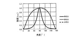
- FIG. 6 shows the angle characteristics of the blue light bl transmitted through the sample 2 and the angle characteristics of the red light rl and the green light gl transmitted through the second light diffusion layer 42 and the third light diffusion layer 43, respectively.
- FIG. 7 shows the angle characteristics of the blue light bl transmitted through the sample 1 and the angle characteristics of the red light rl and the green light gl transmitted through the second light diffusion layer 42 and the third light diffusion layer 43, respectively.
- the Me intensity parameter that determines the scattered light intensity is represented by the particle size parameter ⁇ , the refractive index m of the particle, and the scattering angle ⁇ .
- the particle size parameter ⁇ is generally represented by the following formula.
- Dp is the diameter of the particle
- ⁇ is the wavelength of light.
- ⁇ ( ⁇ ⁇ Dp) / ⁇
- the case where the particle size parameter ⁇ is about 1 is Rayleigh scattering, and the case where the particle size parameter ⁇ is about 3 is Mie scattering. Further, when the particle size parameter ⁇ is 10 or more, it is assumed that the scattering is geometrically expressed (geometric scattering).
- the refractive index m of the particles satisfies the following formula.
- ⁇ is one of parameters indicating the scattering intensity.
- M re is a real term of the refractive index
- mim is an imaginary term of the refractive index.
- the scattered light intensity is derived based on the particle size parameter ⁇ and the refractive index m described above.
- the film thickness corresponding to the thickness of the light diffusion layer
- concentration Since parameters such as (particle dispersion amount) are also required, it is difficult to mathematically determine the scattered light intensity. Therefore, it is common to actually prepare a sample and check the degree of scattering from the result of optical measurement.
- the particles were TiO 2 particles having a refractive index of 2.52 and an average particle diameter of 200 nm, the particle concentration was 15% by mass, and the thickness of the light diffusion layer was 15 ⁇ m.
- the particles were TiO 2 particles having a refractive index of 2.52 and an average particle diameter of 200 nm, the particle concentration was 30% by mass, and the thickness of the light diffusion layer was 15 ⁇ m.
- the particles were SiO 2 particles having a refractive index of 1.59 and an average particle diameter of 2.5 ⁇ m, the particle concentration was 30% by mass, and the thickness of the light diffusion layer was 20 ⁇ m.
- the refractive index of the matrix transparent material
- Fig. 8 shows the simulation results under conditions 1 to 3 (relationship between angle (°) and intensity ratio).
- conditions 1 and 2 in which the average particle diameter of the particles is small, the decrease in strength accompanying an increase in the angle is more gradual than in condition 3 in which the average particle diameter of the particles is large. Then that is remarkable.
- the average particle size of the particles is reduced (specifically, as described above, 500 nm or less is preferable, and 200 nm or less is more preferable), and the particle concentration and the thickness of the light diffusion layer are appropriately adjusted.
- Mie scattering becomes sufficiently dominant.
- a transparent resin layer may be provided in the region 30b corresponding to the blue pixel B of the coloring portion 30.
- the same diffusion layer material as that of the first light diffusion layer 41 is applied to the region 30b, and this region 30b also has a light for diffusing the blue light bl in cooperation with the first light diffusion layer 41 of the light diffusion portion 40. It may function as a diffusion layer.
- the first diffusion layer material formed continuously from the same diffusion layer material over both the region 30 b corresponding to the blue pixel B of the color development portion 30 and the region corresponding to the blue pixel B of the light diffusion portion 40.
- One light diffusion layer 41 may be provided.
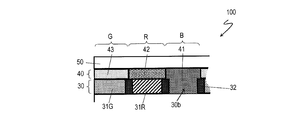
- the second light diffusing layer 42, the third light diffusing layer 43, and the first light diffusing layer 41 are exemplified as being formed of different materials. As shown in FIG. In addition, the second light diffusion layer 42, the third light diffusion layer 43, and the first light diffusion layer 41 may be formed of the same material.
- the first light diffusion layer 41, the second light diffusion layer 42, and the third light diffusion layer 43 are formed from the same diffusion layer material.
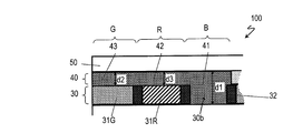
- the thickness d2 of the second light diffusion layer 42 and the thickness d3 of the third light diffusion layer 43 are smaller than the thickness d1 of the first light diffusion layer 41, so that the first light diffusion layer 41 has a thickness d3.
- the light diffusion characteristics are different from the light diffusion characteristics of the second light diffusion layer 42 and the third light diffusion layer 43.
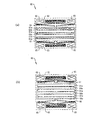
- FIGS. 11A and 11B show examples of specific configurations of the illumination device 10, respectively.
- the illumination device 10 includes a plurality of blue light emitting diodes (blue LEDs) 11 that are light sources, and a reflecting surface 12 provided corresponding to each of the plurality of blue LEDs 11.
- blue LEDs blue light emitting diodes
- Each blue LED 11 emits blue light bl.
- the reflection surface 12 is provided on the back side of the blue LED 11 and reflects the blue light bl emitted from the blue LED 11.
- the reflecting surface 12 has a curved surface shape such that the reflected blue light bl becomes substantially parallel light (typically a parabolic shape). Therefore, the blue light bl is emitted as substantially parallel light from the illumination device 10 illustrated in FIG.
- the illumination device 10 includes a plurality of blue LEDs 11 that are light sources, and a reflecting surface 12 provided corresponding to each of the plurality of blue LEDs 11.
- the reflecting surface 12 does not have a curved surface shape such that the reflected blue light bl becomes substantially parallel light.
- the illumination device 10 shown in FIG. 11B has a lens array 13 provided on the observer side of the blue LED 11.
- the lens array 13 includes a plurality of lenses 13 a each provided corresponding to each of the plurality of blue LEDs 11.
- the blue light bl emitted from the blue LED 11 is collimated by these lenses 13a. Therefore, the blue light bl is emitted as substantially parallel light also from the illumination device 10 illustrated in FIG.
- the parallelism of the blue light bl emitted from the illumination device 10 is preferably as high as possible.
- the half-value angle is preferably ⁇ 10 ° or less, and ⁇ More preferably, it is 5 ° or less.
- FIG. 12 shows a display device 200 according to this embodiment.
- FIG. 12 is a cross-sectional view schematically showing the display device 200.
- the display device 200 in the present embodiment is different from the display device 100 in the first embodiment in that it includes a MEMS shutter array (hereinafter referred to as a MEMS shutter array) 60 as an optical shutter array.
- a MEMS shutter array hereinafter referred to as a MEMS shutter array
- the MEMS shutter array 60 has a mechanical shutter manufactured by a MEMS (Micro Electro Mechanical Systems) technology for each pixel, and each pixel is opened and closed by opening and closing the shutter.
- the light transmittance can be controlled.
- FIGS. 13A and 13B are plan views schematically showing a region corresponding to one pixel of the MEMS shutter array 60.
- FIG. FIG. 13A shows a case where the shutter 61 provided for each pixel is in an open state
- FIG. 13B shows a case where the shutter 61 is in a closed state.
- each pixel of the MEMS shutter array 60 is provided with a shutter 61, and a first actuator 62 and a second actuator 63 connected to the shutter 61. Yes.
- the shutter 61 includes a plurality of (here, three) openings 61a that transmit light.
- each opening 61a is substantially rectangular.
- At least the surface of the shutter 61 other than the opening 61a is made of a material that absorbs or reflects light so as not to transmit light.
- the first actuator 62 and the second actuator 63 are controlled independently of each other.
- the first actuator 62 operates to open the shutter 61.
- the second actuator 63 operates to close the shutter 61.
- the first actuator 62 and the second actuator 63 move the shutter 61 within a certain plane (in a plane parallel to the paper surface of FIGS. 13A and 13B).
- a reflective surface 64 is provided below the shutter 61.
- the reflecting surface 64 is made of a metal film deposited on a transparent substrate such as a plastic substrate or a glass substrate.
- a plurality of (here, three) openings 64 a are formed in the reflective surface 64. In the example shown in FIGS. 13A and 13B, each opening 64a is substantially rectangular.
- the shutter 61, the first actuator 62, and the second actuator 63 are suspended above the reflecting surface 64 by an anchor 65.
- the state of the shutter 61 is switched between the open state shown in FIG. 13A and the closed state shown in FIG.
- the ratio of the period of time in which the shutter 61 is in the closed state the light transmittance in each pixel can be controlled.
- the display device 200 can further improve the light use efficiency. Further, the MEMS shutter array 60 is excellent in response speed (opening / closing speed), and the response speed hardly depends on the ambient temperature. Therefore, by using the MEMS shutter array 60 as the optical shutter array, a high-speed response can be realized even at a low temperature.
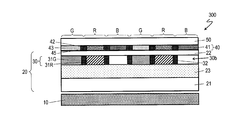
- FIG. 14 shows a display device 300 according to this embodiment.
- FIG. 14 is a cross-sectional view schematically showing the display device 300.
- the display device 300 according to the present embodiment is different from the display device 100 according to the first embodiment in that the red phosphor layer 31R and the green phosphor layer 31G are arranged in the liquid crystal panel 20.
- the color forming section 30 including the red phosphor layer 31R and the green phosphor layer 31G is located between the liquid crystal layer 23 of the liquid crystal panel 20 and the counter substrate 22.
- the counter substrate 22 is formed thinner (for example, up to about 0.05 mm) than the counter substrate 22 in the display device 100 of the first embodiment.
- a light shielding layer 45 is provided in a region corresponding to between the pixels of the light diffusion unit 40.
- the red phosphor layer 31R and the green phosphor layer 31G are arranged in the liquid crystal panel 20, advantages such as thinning, high definition, and weight reduction can be obtained.
- the counter substrate 22 is positioned between the color developing unit 30 and the light diffusing unit 40. If the distance between the color forming portion 30 and the light diffusing portion 40 is large, depending on the pixel size, light emitted from the red phosphor layer 31R or the green phosphor layer 31G enters the light diffusing layer of the pixel adjacent to the corresponding pixel. As a result, the display quality is deteriorated (color mixture occurs). Therefore, it is preferable to form the counter substrate 22 thinly as in this embodiment.
- the light diffusing unit 40 includes a light shielding layer 45 provided in a region corresponding to between pixels as in the present embodiment.
- the width w1 of the light shielding layer 45 of the light diffusing unit 40 is larger than the width w2 of the light shielding layer 32 of the color developing unit 30, as shown in FIG.
- a display device with high light utilization efficiency and a sufficiently small difference in viewing angle characteristics between pixels displaying each primary color is provided.
- Illumination device 11 Blue LED 12 reflective surface 13 lens array 13a lens 20 liquid crystal panel (optical shutter array) 21, 22 Substrate 23 Liquid crystal layer 30 Color developing portion 30b Colored portion corresponding to blue pixel 31R Red phosphor layer 31G Green phosphor layer 32 Light shielding layer 40 Light diffusing portion 41 First light diffusing layer 41a Matrix 41b Particle 42 First 2 light diffusion layers 43 3rd light diffusion layer 45 Light-shielding layer 50 Protection plate 60 MEMS shutter array 100, 200, 300 Display device R Red pixel G Green pixel B Blue pixel rl Red light gl Green light bl Blue light
Landscapes
- Physics & Mathematics (AREA)
- General Physics & Mathematics (AREA)
- Optics & Photonics (AREA)
- Nonlinear Science (AREA)
- Chemical & Material Sciences (AREA)
- Mathematical Physics (AREA)
- Crystallography & Structural Chemistry (AREA)
- Dispersion Chemistry (AREA)
- Liquid Crystal (AREA)
Abstract
表示装置(100)は、青色光(bl)を出射する照明装置(10)と、照明装置(10)から出射された青色光(bl)の透過率を各画素において制御し得る光シャッタアレイ(20)と、赤画素(R)に対応して設けられ、青色光(bl)によって励起されて赤色光(rl)を発する赤色蛍光体層(31R)と、緑画素(G)に対応して設けられ、青色光(bl)によって励起されて緑色光(gl)を発する緑色蛍光体層(31G)と、青画素(B)に対応して設けられ、光シャッタアレイ(20)を透過した青色光(bl)を拡散する第1光拡散層(41)とを備える。第1光拡散層(41)は、ミー散乱により青色光(bl)を拡散する。
Description
本発明は、表示装置に関し、特に、光の利用効率を向上させるために青色光を出射する照明装置が用いられた表示装置に関する。
近年、液晶表示装置は、薄型で低消費電力であるという特長を生かして、ノート型パーソナルコンピュータ、携帯電話、電子手帳などの情報機器、あるいは液晶モニターを備えたカメラ一体型VTRなどに広く用いられている。
各種の表示装置におけるカラー表示は、光の三原色である赤、緑および青を加法混色することにより行われる。一般的な液晶表示装置は、白色光を出射する照明装置(バックライト)を備えており、液晶パネルの赤画素、緑画素、青画素に対応する領域に、赤色光、緑色光、青色光を選択的に透過させるカラーフィルタがそれぞれ設けられている。
しかしながら、一般的な液晶表示装置に採用されている上記の構成では、照明装置から出射した白色光の多くがカラーフィルタで吸収されるので、光の利用効率が低いという問題がある。
そこで、特許文献1および2は、バックライトとして青色光を出射する照明装置が用いられた液晶表示装置を提案している。図16に、特許文献2に開示されている液晶表示装置900を示す。図16は、液晶表示装置900を模式的に示す断面図である。
液晶表示装置900は、図16に示すように、バックライト910、背面側偏光板901、液晶パネル920、観察者側偏光板902、カラーフィルタ903および光散乱フィルム904を有する。これらは、背面側からこの順に設けられている。
バックライト910は、導光板914と、導光板914の端面に配置された青色発光ダイオード(青色LED)911とを有する。導光板914の背面側には、反射シート915が設けられており、青色LED911を囲うように、反射板916が設けられている。導光板914の前面側には、第1拡散シート917、プリズムシート918および第2拡散シート919が設けられている。
液晶パネル920は、一対の基板921および922と、これらの基板921および922間に設けられた液晶層923とを有する。一対の基板921および922のそれぞれの液晶層923側には、電極924aおよび924bが設けられている。また、電極924aおよび924bのそれぞれ上には、液晶層923に接するように、配向膜925aおよび925bが設けられている。
カラーフィルタ903は、赤画素Rに対応する領域に設けられた赤色発色層903R、緑画素Gに対応する領域に設けられた緑色発色層903G、青画素Bに対応する領域に設けられた青色透過層903Bおよび画素間に設けられたブラックマトリクス903BMを有する。赤色発色層903Rは、青色光によって励起されて赤色光を発する蛍光体材料から形成されている。緑色発色層903Gは、青色光によって励起されて緑色光を発する蛍光体材料から形成されている。青色透過層903Bは、少なくとも青色光を透過させる材料から形成されている。このように、液晶表示装置900のカラーフィルタ903は、従来の一般的なカラーフィルタと大きく異なる。
バックライト910から出射した青色光は、背面側偏光板901を介して液晶パネル920に入射する。液晶パネル920は、画素ごとに、青色光を変調して観察者側偏光板902を透過する青色光の量を制御する。観察者側偏光板902を透過した青色光は、カラーフィルタ903に入射する。
カラーフィルタ903の赤画素Rに対応する領域に入射した青色光は、赤色発色層903Rの蛍光体材料を励起し、これにより、赤色発色層903Rが赤色光を発する。カラーフィルタ903の緑画素Gに対応する領域に入射した青色光は、緑色発色層903Gの蛍光体材料を励起し、これにより、緑色発色層903Gが緑色光を発する。カラーフィルタ903の青画素Bに対応する領域に入射した青色光は、青色透過層903Bを通過する。カラーフィルタ903から出射した赤色光、緑色光および青色光は、光散乱フィルム904で散乱される。
このように、液晶表示装置900では、青色光を出射するバックライト910と、青色光によって励起されて赤色光を発する赤色発色層903Rと、青色光によって励起されて緑色光を発する緑色発色層903Gとが設けられていることにより、カラー表示を行うことができる。そのため、従来の一般的な液晶表示装置に採用されている、白色光を出射する照明装置とカラーフィルタとを組み合わせた構成に比べ、光の利用効率が高い。
なお、赤色発色層903Rおよび緑色発色層903Gは、それぞれ赤色光および緑色光を等方的に発する。これに対し、青色透過層903Bは、指向性の高い(つまり平行度の高い)青色光を単純に透過させる。従って、赤色発色層903Rおよび緑色発色層903Gから発せられた赤色光および緑色光と、青色透過層903Bを透過した青色光とは、その角度特性(強度分布)が大きく異なる。
液晶表示装置900では、カラーフィルタ903よりも観察者側に光散乱フィルム904が設けられているので、青色透過層903Bを透過した青色光が、光散乱フィルム904によって散乱される。そのため、赤色光および緑色光と青色光とでの角度特性の差を小さくし、赤画素R、緑画素Gおよび青画素Bの視野角特性の差を小さくすることができる。
しかしながら、特許文献2の液晶表示装置900では、赤画素R、緑画素Gおよび青画素Bに対し、単一の(つまり共通の)光散乱フィルム904が設けられており、もともと大きく異なっている赤色光、緑色光および青色光の角度特性を、すべての色の画素に共通の光散乱フィルム904によってほぼ同じにすることは難しい。そのため、赤画素R、緑画素Gおよび青画素Bの視野角特性を揃えることは実際には困難である。
本発明は、上記問題に鑑みてなされたものであり、その目的は、光の利用効率が高く、且つ、各原色を表示する画素間での視野角特性の差が十分に小さい表示装置を提供することにある。
本発明の実施形態における表示装置は、赤画素、緑画素および青画素を含む複数の画素を有する表示装置であって、青色光を出射する照明装置と、前記照明装置から出射された青色光の透過率を前記複数の画素のそれぞれにおいて制御し得る光シャッタアレイと、前記赤画素に対応して設けられ、青色光によって励起されて赤色光を発する赤色蛍光体層と、前記緑画素に対応して設けられ、青色光によって励起されて緑色光を発する緑色蛍光体層と、前記青画素に対応して設けられ、前記光シャッタアレイを透過した青色光を拡散する第1光拡散層と、を備え、前記第1光拡散層は、ミー散乱により青色光を拡散する。
ある好適な実施形態において、前記第1光拡散層は、透明材料と、前記透明材料中に分散した粒子と、を有し、前記粒子の平均粒径は、500nm以下である。
ある好適な実施形態において、前記粒子の平均粒径は、200nm以下である。
ある好適な実施形態において、前記粒子は、金属元素を含む材料から形成されている。
ある好適な実施形態において、前記粒子は、金属酸化物から形成されている。
ある好適な実施形態において、前記透明材料の屈折率は、1.48以上1.52以下であり、前記第1光拡散層は、前記粒子を5質量%以上30質量%以下含む。
ある好適な実施形態において、前記第1光拡散層のヘイズ値は、93%以上であり、前記第1光拡散層の拡散透過率は、40%以上である。
本発明のある好適な実施形態における表示装置は、前記赤画素に対応して設けられ、前記赤色蛍光体層から発せられた赤色光を拡散する第2光拡散層と、前記緑画素に対応して設けられ、前記緑色蛍光体層から発せられた緑色光を拡散する第3光拡散層と、をさらに備える。
ある好適な実施形態において、前記第1光拡散層と、前記第2光拡散層および前記第3光拡散層とは、互いに異なる材料から形成されている。
ある好適な実施形態において、前記第1光拡散層と、前記第2光拡散層および前記第3光拡散層とは、互いに同じ材料から形成されており、前記第2光拡散層および前記第3光拡散層の厚さは、前記第1光拡散層の厚さよりも小さい。
ある好適な実施形態において、前記光シャッタアレイは、一対の基板と、前記一対の基板間に設けられた液晶層とを有する液晶パネルである。
ある好適な実施形態において、前記赤色蛍光体層および前記緑色蛍光体層は、前記液晶パネル内に配置されている。
ある好適な実施形態において、前記第1光拡散層を含む光拡散部は、前記複数の画素の間に対応する領域に設けられた遮光層を有する。
ある好適な実施形態において、前記照明装置から出射される青色光は、略平行光である。
本発明の実施形態によると、光の利用効率が高く、且つ、各原色を表示する画素間での視野角特性の差が十分に小さい表示装置が提供される。
以下、図面を参照しながら本発明の実施形態を説明する。なお、本発明は以下の実施形態に限定されるものではない。
(実施形態1)
図1に、本実施形態における表示装置100を示す。図1は、表示装置100を模式的に示す断面図である。
図1に、本実施形態における表示装置100を示す。図1は、表示装置100を模式的に示す断面図である。
表示装置100は、図1に示すように、赤を表示する赤画素R、緑を表示する緑画素Gおよび青を表示する青画素Bを含む複数の画素を有する。これら複数の画素は、表示領域内でマトリクス状に配列されている。また、表示装置100は、照明装置10と、液晶パネル20と、赤色蛍光体層31Rおよび緑色蛍光体層31Gと、第1光拡散層41とを備える。
照明装置(バックライト)10は、青色光を出射する。本実施形態では、照明装置10から出射される青色光は、略平行光である。略平行光を出射する照明装置10の具体的な構成については、後に詳述する。
液晶パネル20は、照明装置10の観察者側に配置されている。液晶パネル20は、照明装置10から出射された青色光の透過率を、複数の画素のそれぞれにおいて制御することができる。つまり、液晶パネル20は、光シャッタアレイとして機能する。
液晶パネル20は、具体的には、一対の基板21および22と、一対の基板21および22間に設けられた液晶層23とを有する。液晶パネル20としては、TN(Twisted Nematic)モード、VA(Vertical Alignment)モード、IPS(In-Plane Switching)モード等の種々の表示モード用の液晶パネルを用いることができる。ただし、従来の一般的な液晶パネルとは異なり、液晶パネル20は、カラーフィルタを有していない。一対の基板21および22のうちの背面側の基板21は、典型的には、複数の画素のそれぞれに設けられた薄膜トランジスタ(TFT)および画素電極(いずれも不図示)を有するアクティブマトリクス基板(TFT基板)である。また、多くの表示モード用の液晶パネル20では、一対の基板21および22のうちの観察者側の基板(対向基板)22は、画素電極に対向する対向電極(不図示)を有する。さらに、多くの表示モード用の液晶パネル20は、液晶層23を介して対向する一対の偏光板(不図示)と組み合わせて用いられる。典型的には、一対の偏光板は、基板21および22の外側に設けられている。
赤色蛍光体層31Rおよび緑色蛍光体層31Gは、液晶パネル20の観察者側に配置されている。赤色蛍光体層31Rは、赤画素Rに対応して設けられており、青色光によって励起されて赤色光を発する。緑色蛍光体層31Gは、緑画素Gに対応して設けられ、青色光によって励起されて緑色光を発する。赤色蛍光体層31Rおよび緑色蛍光体層31Gの材料に特に制限はなく、青色光によって励起されて赤色光や緑色光を発する公知の種々の蛍光体材料を、有機系・無機系を問わず用いることができる。例えば、特許文献2に開示されている蛍光体材料を好適に用いることができる。以下では、表示装置100の厚さ方向(表示面法線に沿った方向)において赤色蛍光体層31Rおよび緑色蛍光体層31Gが設けられている部分を包括的に発色部30とも呼ぶ。発色部30の、青画素Bに対応する領域30bには、蛍光体層は設けられていない。この領域30bには、透明な樹脂層が設けられていてもよい。各画素のサイズが100μm~200μm×300μm~600μmである場合、発色部30の厚さ(赤色蛍光体層31Rおよび緑色蛍光体層31Gの厚さ)は、例えば、10μm~30μmである。
図1に例示している構成では、発色部30の、隣接する2つの画素間に対応する領域には、遮光層32が設けられている。赤色蛍光体層31Rおよび緑色蛍光体層31Gからは、等方的に光が発せられるので、このような遮光層32が設けられていることにより、他の画素に光が漏れることを防止することができる。遮光層32の材料としては、例えば黒色樹脂を用いることができる。発色部30は、一対の偏光板のうちの観察者側の偏光板の上に設けられていてもよいし、その下に(つまり観察者側の偏光板と対向基板22との間に)設けられていてもよい。前者の配置を採用すると、後者の配置に比べ赤色蛍光体層31Rおよび緑色蛍光体層31Gがより観察者側に位置するため、視野角特性が良いという利点が得られる。
第1光拡散層41は、青画素Bに対応して設けられ、光シャッタアレイである液晶パネル20を透過した青色光を拡散する。この第1光拡散層41は、ミー散乱により青色光を拡散する。ミー散乱とは、粒子による光の散乱現象の一種である。
本実施形態における表示装置100は、さらに、第2光拡散層42と、第3光拡散層43とを備える。第2光拡散層42は、赤画素Rに対応して設けられ、赤色蛍光体層31Rから発せられた赤色光を拡散する。第3光拡散層43は、緑画素Gに対応して設けられ、緑色蛍光体層31Gから発せられた緑色光を拡散する。第2光拡散層42および第3光拡散層43と、第1光拡散層41とは、互いに異なる材料から形成されている。以下では、表示装置100の厚さ方向において第1光拡散層41、第2光拡散層42および第3光拡散層43が設けられている部分を包括的に光拡散部40と呼ぶ。光拡散部40の厚さは、例えば、5μm~30μmである。
光拡散部40上には、透明な保護板50が設けられている。保護板50は、例えば、薄いガラス板である。
上述した構成を有する表示装置100では、以下のようにして表示が行われる。図2に、表示装置100が表示を行っている様子を示す。
図2に示すように、照明装置10から出射した青色光blは、液晶パネル20に入射する。光シャッタアレイである液晶パネル20は、画素ごとに、青色光blの透過率を制御する。液晶パネル20を透過した青色光blは、発色部30に入射する。
発色部30に入射した青色光blの一部は、赤色蛍光体層31Rを励起する。これにより、赤色蛍光体層31Rが赤色光rlを発する。このとき、赤色光rlは等方的に発せられる。発色部30に入射した青色光blの他の一部は、緑色蛍光体層31Gを励起する。これにより、緑色蛍光体層31Gが緑色光glを発する。このとき、緑色光glは等方的に発せられる。発色部30に入射した青色光blのさらに他の一部は、青画素Bに対応する領域30b(蛍光体層が設けられていない)を通過する。このとき、青色光blは、略平行光のままである。
発色部30からの光は、光拡散部40で拡散される。具体的には、発色部30の青画素Bに対応する領域30bを通過してきた青色光blは、第1光拡散層41によって拡散される。赤色蛍光体層31Rから発せられた赤色光rlは、第2光拡散層42によって拡散される。緑色蛍光体層31Gから発せられた緑色光glは、第3光拡散層43によって拡散される。
上述したように、表示装置100では、青色光blを出射する照明装置10と、青色光blによって励起されて赤色光rlを発する赤色蛍光体層31Rと、青色光blによって励起されて緑色光glを発する緑色蛍光体層31Gとが設けられていることにより、カラー表示を行うことができる。そのため、従来の一般的な液晶表示装置に採用されている、白色光を出射する照明装置とカラーフィルタとを組み合わせた構成に比べ、光の利用効率が高い。
また、表示装置100では、青画素Bと、赤画素Rおよび緑画素Gとで、別個に光拡散層が設けられている。具体的には、青画素Bに対しては第1光拡散層41が設けられ、赤画素Rに対しては第2光拡散層42が設けられ、緑画素Gに対しては第3光拡散層43が設けられている。そのため、青色光blの角度特性と、赤色光rlおよび緑色光glの角度特性との差を、光拡散部40によって十分に小さくすることができる。
さらに、表示装置100では、第1光拡散層41は、ミー散乱によって青色光blを拡散する。そのため、第1光拡散層41では、液晶表示装置の光学素子として一般的に用いられている光拡散層、つまり、幾何学的散乱によって光を拡散する光拡散層に比べ、より等方的に光が拡散(散乱)される。それ故、照明装置10から出射する青色光blが略平行光であっても、青色光blの角度特性と、赤色光rlおよび緑色光glの角度特性とを十分に近く(例えばほぼ同じに)することができる。そのため、本実施形態の表示装置100では、赤画素R、緑画素Gおよび青画素B間での視野角特性の差を十分に小さくすることができる。
ここで、青画素Bに対応して設けられる(つまり青色光blを拡散するための)第1光拡散層41の具体的な構成を説明する。
図3に、第1光拡散層41の具体的な構成の例を示す。図3に示す第1光拡散層41は、透明材料から形成されたマトリクス41aと、マトリクス41a中に分散した粒子41bとを有する。
マトリクス41aの材料である透明材料は、典型的には樹脂材料である。樹脂材料の種類は特に限定されず、樹脂材料としては、例えば熱可塑性樹脂や熱硬化性樹脂を好適に用いることができる。具体的な樹脂材料としては、例えば、アクリル樹脂やポリカーボネート、ポリエステルを用いることができる。アクリル樹脂、ポリカーボネートおよびポリエステルの屈折率は、それぞれ1.49、1.59および1.6である。
粒子41bは、典型的には、金属元素を含む材料から形成されており、例えば金属酸化物から形成されている。金属元素としては、例えば、チタン(Ti)、ジルコニウム(Zr)、アルミニウム(Al)、スズ(Sn)およびアンチモン(Sb)が挙げられ、金属酸化物としては、例えば、TiO2、ZrO2、Al2O3、SnO2およびSb2O3が挙げられる。TiO2、ZrO2、Al2O3、SnO2およびSb2O3の屈折率は、それぞれ2.71、2.15、1.63、2.03および2.1である。
第1光拡散層41での光散乱においてミー散乱を十分に支配的にするためには、粒子41bの平均粒径は、500nm以下であることが好ましく、200nm以下であることがより好ましい。ただし、散乱強度を十分に大きくする観点からは、粒子41bの平均粒径は、250nm以上であることが好ましい。
ミー散乱により青色光blを拡散する好適な構成の例としては、例えば、1.48以上1.52以下の屈折率を有するマトリクス(透明材料)41aに、粒子41bを5質量%以上30質量%以下分散させた構成を挙げることができる。
略平行光である青色光blを十分に拡散させる観点からは、第1光拡散層41のヘイズ値は、93%以上であることが好ましく、第1光拡散層41の拡散透過率は、40%以上であることが好ましい。
第2光拡散層42および第3光拡散層43も、典型的には、透明材料から形成されたマトリクスと、マトリクス中に分散した粒子とを有する。ただし、第2光拡散層42および第3光拡散層43のそれぞれの光拡散特性は、第1光拡散層41の光拡散特性と異なる。第2光拡散層42および第3光拡散層43のそれぞれは、ミー散乱により光を拡散させるものであってもよいし、幾何学的散乱により光を拡散させるものであってもよい。幾何学的散乱により光を拡散させる場合、粒子の平均粒径は、典型的には、10μm以上である。
続いて、図4(a)~(f)を参照しながら、第1光拡散層41を含む光拡散部40の形成方法を説明する。図4(a)~(f)は、光拡散部40の形成工程を示す工程断面図である。
まず、図4(a)に示すように、保護板50を用意する。保護板50としてガラス板を用いる場合、その厚さは例えば0.3mm~1.0mm程度である。
次に、図4(b)に示すように、保護板50上に、壁状構造体45を形成する。壁状構造体45は、画素間に位置するように設けられ、遮光層として機能する。壁状構造体(遮光層)45の材料としては、液晶パネルのブラックマトリクスに用いられる材料や、遮光性を有する樹脂材料を用いることができる。
続いて、図4(c)に示すように、第1光拡散層41を形成する。具体的には、保護板50上の青画素Bに対応する領域に、マトリクス41aとなる透明材料と粒子41bとを含む拡散層材料を塗布することにより、第1光拡散層41を形成する。粒子41bの分散量(濃度)は、青色光blを好適に拡散できるように調整されている。
次に、図4(d)に示すように、第2光拡散層42を形成する。具体的には、保護板50上の赤画素Rに対応する領域に、マトリクスとなる透明材料と粒子とを含む拡散層材料を塗布することにより、第2光拡散層42を形成する。粒子の分散量(濃度)は、赤色光rlを好適に拡散できるように調整されている。
続いて、図4(e)に示すように、第3光拡散層43を形成する。具体的には、保護板50上の緑画素Gに対応する領域に、マトリクスとなる透明材料と粒子とを含む拡散層材料を塗布することにより、第3光拡散層43を形成する。粒子の分散量(濃度)は、緑色光glを好適に拡散できるように調整されている。なお、第1光拡散層41、第2光拡散層42および第3光拡散層43を形成するための拡散層材料は、例えば、インクジェット法により塗布することができる。あるいは、高精度ディスペンサーを用いて塗布を行うこともできる。このようにして、第1光拡散層41、第2光拡散層42および第3光拡散層43を含む光拡散部40を形成することができる。
その後、図4(f)に示すように、光拡散部40(および保護板50)は、液晶パネル20の観察者側に設けられた発色部30に接合される。光拡散部40の発色部30への接合は、例えば、紫外線硬化性樹脂や熱硬化性樹脂を用いて行われる。
続いて、ミー散乱を利用する第1光拡散層41と、幾何学的散乱を利用する光拡散層とを実際に試作して(それぞれサンプル1、2と呼ぶ)それらに略平行光を入射させ、透過した光(拡散された光)の角度特性を測定した結果を説明する。
サンプル1の作製に際しては、マトリクス41aとなる透明材料として、屈折率が1.51の樹脂材料を用い、粒子41bとして、平均粒径が約200nmで屈折率が2.52のTiO2粒子を用いた。サンプル2の作製に際しては、マトリクスとなる透明材料として、屈折率が1.51の樹脂材料を用い、粒子として、平均粒径が約5μmで屈折率が1.59のSiO2粒子を用いた。
図5に、サンプル1および2を透過した光の角度特性(角度(°)と強度(a.u.)との関係)を示す。図5からわかるように、幾何学的散乱を利用するサンプル2の場合、透過光の強度は、0°付近において著しく高く、角度が大きくなるにつれて急激に低くなる。これに対し、ミー散乱を利用するサンプル1の場合、透過光の強度は、角度が大きくなるにつれて緩やかに低くなる。このように、ミー散乱を利用することで、より等方的な光拡散が可能になることがわかる。
図6に、サンプル2を透過した青色光blの角度特性と、第2光拡散層42および第3光拡散層43をそれぞれ透過した赤色光rlおよび緑色光glの角度特性とを示す。また、図7に、サンプル1を透過した青色光blの角度特性と、第2光拡散層42および第3光拡散層43をそれぞれ透過した赤色光rlおよび緑色光glの角度特性とを示す。
図6からわかるように、サンプル2を青色光blを拡散させるために用いると、青色光blの角度特性と、赤色光rlおよび緑色光glの角度特性とが大きく異なってしまう。これに対し、図7からわかるように、サンプル1を青色光blを拡散させるために用いると、青色光blの角度特性と、赤色光rlおよび緑色光glの角度特性とをほぼ同じにすることができる。
ここで、ミー散乱における散乱光強度に関係するパラメータを説明する。
散乱光強度を決定するミー強度パラメータは、粒径パラメータα、粒子の屈折率mおよび散乱角θによって表される。
粒径パラメータαは、一般に、下記式で表される。下記式において、Dpは粒子の直径であり、λは光の波長である。
α=(π・Dp)/λ
α=(π・Dp)/λ
粒径パラメータαが1程度の場合がレイリー散乱であり、粒径パラメータαが3程度の場合がミー散乱であるとされる。また、粒径パラメータαが10以上の場合は、幾何学的に表現される散乱(幾何学的散乱)であるとされる。
また、粒子の屈折率mは、下記式を満足する。下記式において、βは散乱強度を示すパラメータの1つである。また、mreは屈折率の実数項であり、mimは屈折率の虚数項である。
β=m・α
m=mre-i・mim
β=m・α
m=mre-i・mim
上述した粒径パラメータαおよび屈折率mに基づいて、散乱光強度を導き出すことになるが、粒径パラメータαおよび屈折率mの他に膜厚(光拡散層の厚さに相当する)や濃度(粒子の分散量)などのパラメータも必要とされるので、数学的に散乱光強度を求めることは難しい。そのため、実際に試料を作製し、光学測定の結果から散乱度合を確認することが一般的である。
続いて、粒子の平均粒径、屈折率、濃度(分散量)、光拡散層の厚さをパラメータとしてシミュレーションを行った結果の一部(3つの条件1~3)を説明する。
条件1では、粒子を屈折率が2.52で平均粒径が200nmのTiO2粒子とし、粒子濃度を15質量%とし、光拡散層の厚さを15μmとした。条件2では、粒子を屈折率が2.52で平均粒径が200nmのTiO2粒子とし、粒子濃度を30質量%とし、光拡散層の厚さを15μmとした。条件3では、粒子を屈折率が1.59で平均粒径が2.5μmのSiO2粒子とし、粒子濃度を30質量%とし、光拡散層の厚さを20μmとした。なお、条件1~3のいずれについても、マトリクス(透明材料)の屈折率を1.51とした。
図8に、条件1~3のシミュレーション結果(角度(°)と強度比率との関係)を示す。図8からわかるように、粒子の平均粒径が小さい条件1および2では、粒子の平均粒径が大きい条件3に比べ、角度が大きくなることに伴う強度の低下が緩やかであり、特に条件2ではそれが顕著である。このように、粒子の平均粒径を小さくする(具体的には既に説明したように500nm以下が好ましく、200nm以下がより好ましい)とともに、粒子濃度や光拡散層の厚さを適切に調整することにより、ミー散乱が十分に支配的になることが確認された。
なお、上述の説明において、発色部30の、青画素Bに対応する領域30bに透明な樹脂層が設けられていてもよいことを述べた。しかしながら、この領域30bに、第1光拡散層41と同じ拡散層材料を付与し、この領域30bも光拡散部40の第1光拡散層41と協同的に青色光blを拡散させるための光拡散層として機能させてもよい。例えば、図9に示すように、発色部30の青画素Bに対応する領域30bおよび光拡散部40の青画素Bに対応する領域の両方にわたって、同じ拡散層材料から連続的に形成された第1光拡散層41を設けてもよい。
また、上述の説明では、第2光拡散層42および第3光拡散層43と、第1光拡散層41とは、互いに異なる材料から形成されている構成を例示したが、図10に示すように、第2光拡散層42および第3光拡散層43と、第1光拡散層41とが互いに同じ材料から形成されていてもよい。
図10に示す構成では、第1光拡散層41と、第2光拡散層42および第3光拡散層43とは、同じ拡散層材料から形成されている。ただし、第2光拡散層42の厚さd2および第3光拡散層43の厚さd3は、第1光拡散層41の厚さd1よりも小さく、そのことによって、第1光拡散層41の光拡散特性と、第2光拡散層42および第3光拡散層43の光拡散特性とが異なっている。このような構成を採用すると、第1光拡散層41と、第2光拡散層42および第3光拡散層43とを同じ拡散層材料を用いて同じ工程で形成することができるので、表示装置100を製造する際の工程数を削減して製造コストの低減を図ることができる。
次に、略平行光を出射し得る照明装置10の具体的な構成を説明する。図11(a)および(b)に、照明装置10の具体的な構成の例をそれぞれ示す。
図11(a)に示す例では、照明装置10は、光源である複数の青色発光ダイオード(青色LED)11と、複数の青色LED11のそれぞれに対応して設けられた反射面12とを有する。
各青色LED11は、青色光blを発する。
反射面12は、青色LED11の背面側に設けられており、青色LED11から発せられた青色光blを反射する。反射面12は、反射された青色光blが略平行光となるような曲面形状を有する(典型的には放物面状である)。そのため、図11(a)に示す照明装置10からは、青色光blが略平行光として出射される。
図11(b)に示す例でも、照明装置10は、光源である複数の青色LED11と、複数の青色LED11のそれぞれに対応して設けられた反射面12とを有する。ただし、図11(b)に示す例では、反射面12は、反射された青色光blが略平行光となるような曲面形状を有しているわけではない。
図11(b)に示す照明装置10は、青色LED11の観察者側に設けられたレンズアレイ13を有する。レンズアレイ13は、それぞれが複数の青色LED11のそれぞれに対応して設けられた複数のレンズ13aを含む。これらのレンズ13aにより、青色LED11から発せられた青色光blが平行化される。そのため、図11(b)に示す照明装置10からも、青色光blが略平行光として出射される。
なお、表示品位を高くする観点からは、照明装置10から出射される青色光blの平行度ができるだけ高いことが好ましく、具体的には、半値角が±10°以下であることが好ましく、±5°以下であることがより好ましい。
(実施形態2)
図12に、本実施形態における表示装置200を示す。図12は、表示装置200を模式的に示す断面図である。
図12に、本実施形態における表示装置200を示す。図12は、表示装置200を模式的に示す断面図である。
本実施形態における表示装置200は、光シャッタアレイとしてMEMS方式のシャッタアレイ(以下ではMEMSシャッタアレイと呼ぶ)60を備える点において、実施形態1における表示装置100と異なっている。MEMSシャッタアレイ60は、図12には示していないが、画素ごとに、MEMS(Micro Electro Mechanical Systems)技術により作製された機械式のシャッタを有しており、このシャッタの開閉により、画素ごとに光の透過率を制御することができる。
MEMSシャッタアレイ60の具体的な構成の例を図13(a)および(b)に示す。図13(a)および(b)は、MEMSシャッタアレイ60の1つの画素に対応する領域を模式的に示す平面図である。図13(a)は、画素ごとに設けられたシャッタ61が開状態にある場合を示し、図13(b)は、シャッタ61が閉状態にある場合を示している。
MEMSシャッタアレイ60の各画素には、図13(a)および(b)に示すように、シャッタ61と、シャッタ61に連結された第1のアクチュエータ62および第2のアクチュエータ63とが設けられている。
シャッタ61は、光を透過させる複数の(ここでは3つの)開口部61aを含む。図13(a)および(b)に示す例では、各開口部61aは、略矩形である。シャッタ61の、開口部61a以外の部分は、光を透過させないように少なくともその表面が光を吸収または反射する材料で形成されている。
第1のアクチュエータ62および第2のアクチュエータ63は、互いに独立に制御される。第1のアクチュエータ62は、シャッタ61を開くように動作する。これに対し、第2のアクチュエータ63は、シャッタ61を閉じるように動作する。第1のアクチュエータ62および第2のアクチュエータ63は、シャッタ61をある平面内(図13(a)および(b)の紙面に平行な面内)で移動させる。
シャッタ61の下方には、反射面64が設けられている。反射面64は、例えば、プラスチック基板やガラス基板などの透明基板上に蒸着された金属膜によって構成されている。反射面64には、複数の(ここでは3つの)開口部64aが形成されている。図13(a)および(b)に示す例では、各開口部64aは、略矩形である。シャッタ61、第1のアクチュエータ62および第2のアクチュエータ63は、アンカー65によって、反射面64の上方に吊るされている。
第1のアクチュエータ62および第2のアクチュエータ63によって、シャッタ61の状態を、図13(a)に示す開状態と、図13(b)に示す閉状態との間で切り替え、シャッタ61が開状態にある時間と、シャッタ61が閉状態にある時間との比率を調節することにより、各画素における光の透過率を制御することができる。
上述した構成を有するMEMSシャッタアレイ60は、偏光板が不要であるので、本実施形態における表示装置200では、光の利用効率のいっそうの向上を図ることが可能になる。また、MEMSシャッタアレイ60は、応答速度(開閉速度)に優れる上に応答速度が周囲の温度に依存しにくい。そのため、光シャッタアレイとしてMEMSシャッタアレイ60を用いることにより、低温でも高速応答を実現することができる。
(実施形態3)
図14に、本実施形態における表示装置300を示す。図14は、表示装置300を模式的に示す断面図である。
図14に、本実施形態における表示装置300を示す。図14は、表示装置300を模式的に示す断面図である。
本実施形態における表示装置300は、赤色蛍光体層31Rおよび緑色蛍光体層31Gが液晶パネル20内に配置されている点において、実施形態1における表示装置100と異なっている。
表示装置300では、図14に示すように、赤色蛍光体層31Rおよび緑色蛍光体層31Gを含む発色部30は、液晶パネル20の液晶層23と対向基板22との間に位置している。対向基板22は、実施形態1の表示装置100における対向基板22に比べ、薄く(例えば0.05mm程度まで)形成されている。また、光拡散部40の画素間に対応する領域には、遮光層45が設けられている。
本実施形態における表示装置300では、赤色蛍光体層31Rおよび緑色蛍光体層31Gが液晶パネル20内に配置されているので、薄型化、高精細化、軽量化などの利点が得られる。
なお、赤色蛍光体層31Rおよび緑色蛍光体層31Gを液晶パネル20内に配置する場合、発色部30と光拡散部40との間に対向基板22が位置することになる。発色部30と光拡散部40との間隔が大きいと、画素サイズによっては、赤色蛍光体層31Rや緑色蛍光体層31Gから発せられる光が、対応する画素に隣接した画素の光拡散層に入射してしまい、表示品位の低下(混色の発生)の原因となる。そのため、本実施形態のように、対向基板22を薄く形成することが好ましい。
また、上述したような表示品位の低下を抑制するために、光拡散部40は、本実施形態のように、画素間に対応する領域に設けられた遮光層45を有することが好ましい。その場合、さらに、図15に示すように、光拡散部40の遮光層45の幅w1が、発色部30の遮光層32の幅w2よりも大きいことがさらに好ましい。
本発明の実施形態によると、光の利用効率が高く、且つ、各原色を表示する画素間での視野角特性の差が十分に小さい表示装置が提供される。
10 照明装置
11 青色LED
12 反射面
13 レンズアレイ
13a レンズ
20 液晶パネル(光シャッタアレイ)
21、22 基板
23 液晶層
30 発色部
30b 発色部の、青画素に対応する領域
31R 赤色蛍光体層
31G 緑色蛍光体層
32 遮光層
40 光拡散部
41 第1光拡散層
41a マトリクス
41b 粒子
42 第2光拡散層
43 第3光拡散層
45 遮光層
50 保護板
60 MEMSシャッタアレイ
100、200、300 表示装置
R 赤画素
G 緑画素
B 青画素
rl 赤色光
gl 緑色光
bl 青色光
11 青色LED
12 反射面
13 レンズアレイ
13a レンズ
20 液晶パネル(光シャッタアレイ)
21、22 基板
23 液晶層
30 発色部
30b 発色部の、青画素に対応する領域
31R 赤色蛍光体層
31G 緑色蛍光体層
32 遮光層
40 光拡散部
41 第1光拡散層
41a マトリクス
41b 粒子
42 第2光拡散層
43 第3光拡散層
45 遮光層
50 保護板
60 MEMSシャッタアレイ
100、200、300 表示装置
R 赤画素
G 緑画素
B 青画素
rl 赤色光
gl 緑色光
bl 青色光
Claims (14)
- 赤画素、緑画素および青画素を含む複数の画素を有する表示装置であって、
青色光を出射する照明装置と、
前記照明装置から出射された青色光の透過率を前記複数の画素のそれぞれにおいて制御し得る光シャッタアレイと、
前記赤画素に対応して設けられ、青色光によって励起されて赤色光を発する赤色蛍光体層と、
前記緑画素に対応して設けられ、青色光によって励起されて緑色光を発する緑色蛍光体層と、
前記青画素に対応して設けられ、前記光シャッタアレイを透過した青色光を拡散する第1光拡散層と、を備え、
前記第1光拡散層は、ミー散乱により青色光を拡散する表示装置。 - 前記第1光拡散層は、透明材料と、前記透明材料中に分散した粒子と、を有し、
前記粒子の平均粒径は、500nm以下である請求項1に記載の表示装置。 - 前記粒子の平均粒径は、200nm以下である請求項2に記載の表示装置。
- 前記粒子は、金属元素を含む材料から形成されている請求項1から3のいずれかに記載の表示装置。
- 前記粒子は、金属酸化物から形成されている請求項4に記載の表示装置。
- 前記透明材料の屈折率は、1.48以上1.52以下であり、
前記第1光拡散層は、前記粒子を5質量%以上30質量%以下含む請求項2から5のいずれかに記載の表示装置。 - 前記第1光拡散層のヘイズ値は、93%以上であり、
前記第1光拡散層の拡散透過率は、40%以上である請求項1から6のいずれかに記載の表示装置。 - 前記赤画素に対応して設けられ、前記赤色蛍光体層から発せられた赤色光を拡散する第2光拡散層と、
前記緑画素に対応して設けられ、前記緑色蛍光体層から発せられた緑色光を拡散する第3光拡散層と、をさらに備える請求項1から7のいずれかに記載の表示装置。 - 前記第1光拡散層と、前記第2光拡散層および前記第3光拡散層とは、互いに異なる材料から形成されている請求項8に記載の表示装置。
- 前記第1光拡散層と、前記第2光拡散層および前記第3光拡散層とは、互いに同じ材料から形成されており、
前記第2光拡散層および前記第3光拡散層の厚さは、前記第1光拡散層の厚さよりも小さい請求項8に記載の表示装置。 - 前記光シャッタアレイは、一対の基板と、前記一対の基板間に設けられた液晶層とを有する液晶パネルである請求項1から10のいずれかに記載の表示装置。
- 前記赤色蛍光体層および前記緑色蛍光体層は、前記液晶パネル内に配置されている請求項11に記載の表示装置。
- 前記第1光拡散層を含む光拡散部は、前記複数の画素の間に対応する領域に設けられた遮光層を有する請求項12に記載の表示装置。
- 前記照明装置から出射される青色光は、略平行光である請求項1から13のいずれかに記載の表示装置。
Applications Claiming Priority (2)
| Application Number | Priority Date | Filing Date | Title |
|---|---|---|---|
| JP2011-131538 | 2011-06-13 | ||
| JP2011131538 | 2011-06-13 |
Publications (1)
| Publication Number | Publication Date |
|---|---|
| WO2012173037A1 true WO2012173037A1 (ja) | 2012-12-20 |
Family
ID=47357026
Family Applications (1)
| Application Number | Title | Priority Date | Filing Date |
|---|---|---|---|
| PCT/JP2012/064666 Ceased WO2012173037A1 (ja) | 2011-06-13 | 2012-06-07 | 表示装置 |
Country Status (1)
| Country | Link |
|---|---|
| WO (1) | WO2012173037A1 (ja) |
Cited By (1)
| Publication number | Priority date | Publication date | Assignee | Title |
|---|---|---|---|---|
| WO2020042652A1 (zh) * | 2018-08-31 | 2020-03-05 | 昆山工研院新型平板显示技术中心有限公司 | Led显示器件及其制造方法、led显示面板 |
Citations (2)
| Publication number | Priority date | Publication date | Assignee | Title |
|---|---|---|---|---|
| JP2009244383A (ja) * | 2008-03-28 | 2009-10-22 | Fujifilm Corp | 液晶表示装置 |
| JP2010197791A (ja) * | 2009-02-26 | 2010-09-09 | Sony Corp | カラー液晶表示装置組立体及び光変換装置 |
-
2012
- 2012-06-07 WO PCT/JP2012/064666 patent/WO2012173037A1/ja not_active Ceased
Patent Citations (2)
| Publication number | Priority date | Publication date | Assignee | Title |
|---|---|---|---|---|
| JP2009244383A (ja) * | 2008-03-28 | 2009-10-22 | Fujifilm Corp | 液晶表示装置 |
| JP2010197791A (ja) * | 2009-02-26 | 2010-09-09 | Sony Corp | カラー液晶表示装置組立体及び光変換装置 |
Cited By (2)
| Publication number | Priority date | Publication date | Assignee | Title |
|---|---|---|---|---|
| WO2020042652A1 (zh) * | 2018-08-31 | 2020-03-05 | 昆山工研院新型平板显示技术中心有限公司 | Led显示器件及其制造方法、led显示面板 |
| US11107949B2 (en) | 2018-08-31 | 2021-08-31 | Chengdu Vistar Optoelectronics Co., Ltd. | LED display device, method for manufacturing the same, and LED display panel |
Similar Documents
| Publication | Publication Date | Title |
|---|---|---|
| US10302986B2 (en) | Display device | |
| US8223295B2 (en) | Optical element, liquid crystal panel, and liquid crystal display | |
| JP6008490B2 (ja) | ディスプレイ装置 | |
| CN104503129B (zh) | 一种光学模组和反射型显示装置 | |
| US20130208201A1 (en) | Display device | |
| CN102759818B (zh) | 显示装置 | |
| JP2007004104A5 (ja) | ||
| CN110646989A (zh) | 显示面板、显示装置及其控制方法 | |
| TW200831987A (en) | Transreflective type LCD panel and LCD device using the same | |
| US8625056B2 (en) | Liquid crystal display | |
| WO2020116050A1 (ja) | 光学装置 | |
| CN113589583A (zh) | 显示装置 | |
| KR20120056528A (ko) | 반사형 폴리머 분산 액정 디스플레이 장치 | |
| KR20120049018A (ko) | 표시 장치 | |
| US7619703B2 (en) | Liquid crystal display | |
| WO2018223734A1 (zh) | 显示面板及其显示方法、显示装置 | |
| CN103309077B (zh) | 液晶显示器 | |
| JP2017090774A (ja) | 表示装置 | |
| WO2012173037A1 (ja) | 表示装置 | |
| CN101256302A (zh) | 半透式液晶显示面板与应用其的液晶显示装置 | |
| CN216210335U (zh) | 显示装置 | |
| KR102128924B1 (ko) | 액정표시장치 및 그 제조방법 | |
| JP2001183646A (ja) | 液晶表示装置 | |
| CN222506720U (zh) | 显示面板及显示装置 | |
| JP2013164429A (ja) | カラーフィルタおよびこれを備えた反射型表示装置 |
Legal Events
| Date | Code | Title | Description |
|---|---|---|---|
| 121 | Ep: the epo has been informed by wipo that ep was designated in this application |
Ref document number: 12799787 Country of ref document: EP Kind code of ref document: A1 |
|
| NENP | Non-entry into the national phase |
Ref country code: DE |
|
| 122 | Ep: pct application non-entry in european phase |
Ref document number: 12799787 Country of ref document: EP Kind code of ref document: A1 |
|
| NENP | Non-entry into the national phase |
Ref country code: JP |