WO2012172933A1 - 窒化物半導体装置およびその製造方法 - Google Patents
窒化物半導体装置およびその製造方法 Download PDFInfo
- Publication number
- WO2012172933A1 WO2012172933A1 PCT/JP2012/062952 JP2012062952W WO2012172933A1 WO 2012172933 A1 WO2012172933 A1 WO 2012172933A1 JP 2012062952 W JP2012062952 W JP 2012062952W WO 2012172933 A1 WO2012172933 A1 WO 2012172933A1
- Authority
- WO
- WIPO (PCT)
- Prior art keywords
- nitride semiconductor
- semiconductor layer
- layer
- tial
- semiconductor device
- Prior art date
- Legal status (The legal status is an assumption and is not a legal conclusion. Google has not performed a legal analysis and makes no representation as to the accuracy of the status listed.)
- Ceased
Links
Images





Classifications
-
- H—ELECTRICITY
- H10—SEMICONDUCTOR DEVICES; ELECTRIC SOLID-STATE DEVICES NOT OTHERWISE PROVIDED FOR
- H10D—INORGANIC ELECTRIC SEMICONDUCTOR DEVICES
- H10D64/00—Electrodes of devices having potential barriers
- H10D64/20—Electrodes characterised by their shapes, relative sizes or dispositions
- H10D64/23—Electrodes carrying the current to be rectified, amplified, oscillated or switched, e.g. sources, drains, anodes or cathodes
- H10D64/251—Source or drain electrodes for field-effect devices
-
- H—ELECTRICITY
- H10—SEMICONDUCTOR DEVICES; ELECTRIC SOLID-STATE DEVICES NOT OTHERWISE PROVIDED FOR
- H10D—INORGANIC ELECTRIC SEMICONDUCTOR DEVICES
- H10D30/00—Field-effect transistors [FET]
- H10D30/01—Manufacture or treatment
- H10D30/015—Manufacture or treatment of FETs having heterojunction interface channels or heterojunction gate electrodes, e.g. HEMT
-
- H—ELECTRICITY
- H10—SEMICONDUCTOR DEVICES; ELECTRIC SOLID-STATE DEVICES NOT OTHERWISE PROVIDED FOR
- H10D—INORGANIC ELECTRIC SEMICONDUCTOR DEVICES
- H10D30/00—Field-effect transistors [FET]
- H10D30/40—FETs having zero-dimensional [0D], one-dimensional [1D] or two-dimensional [2D] charge carrier gas channels
- H10D30/47—FETs having zero-dimensional [0D], one-dimensional [1D] or two-dimensional [2D] charge carrier gas channels having two-dimensional [2D] charge carrier gas channels, e.g. nanoribbon FETs or high electron mobility transistors [HEMT]
- H10D30/471—High electron mobility transistors [HEMT] or high hole mobility transistors [HHMT]
- H10D30/475—High electron mobility transistors [HEMT] or high hole mobility transistors [HHMT] having wider bandgap layer formed on top of lower bandgap active layer, e.g. undoped barrier HEMTs such as i-AlGaN/GaN HEMTs
- H10D30/4755—High electron mobility transistors [HEMT] or high hole mobility transistors [HHMT] having wider bandgap layer formed on top of lower bandgap active layer, e.g. undoped barrier HEMTs such as i-AlGaN/GaN HEMTs having wide bandgap charge-carrier supplying layers, e.g. modulation doped HEMTs such as n-AlGaAs/GaAs HEMTs
-
- H—ELECTRICITY
- H10—SEMICONDUCTOR DEVICES; ELECTRIC SOLID-STATE DEVICES NOT OTHERWISE PROVIDED FOR
- H10D—INORGANIC ELECTRIC SEMICONDUCTOR DEVICES
- H10D64/00—Electrodes of devices having potential barriers
- H10D64/111—Field plates
Definitions
- the present invention relates to a nitride semiconductor device and a manufacturing method thereof.
- an oxygen plasma treatment is performed on the surface of an n-type GaN contact layer to form an oxygen doped layer, and then an ohmic electrode is formed on the n-type GaN contact layer, thereby forming an n-type GaN.
- the ohmic electrode has a high contact resistance and a sufficiently low contact resistance. I just could't get it.
- an object of the present invention is to provide a nitride semiconductor device capable of reducing the contact resistance between the nitride semiconductor layer and the ohmic electrode and a method for manufacturing the same.
- the present inventor has found that the TiAl-based material is used. It has been discovered that the contact resistance characteristics of the nitride semiconductor layer and the ohmic electrode change depending on the oxygen concentration in the ohmic electrode when the oxygen atom is contained in the ohmic electrode as an impurity to the extent that an oxide cannot be formed. .
- the present invention has been found for the first time by experiments that the contact resistance is greatly reduced when the oxygen concentration in the ohmic electrode is within a specific range based on the discovery of the present inventors.
- the nitride semiconductor device of the first invention is A substrate, A nitride semiconductor layer formed on the substrate; An ohmic electrode made of a TiAl-based material formed on the nitride semiconductor layer, The oxygen concentration in the ohmic electrode made of the TiAl-based material is 1 ⁇ 10 16 cm ⁇ 3 or more and 1 ⁇ 10 20 cm ⁇ 3 or less.
- the nitride semiconductor of the nitride semiconductor device may be any material represented by Al x In y Ga 1-xy N (x ⁇ 0, y ⁇ 0, 0 ⁇ x + y ⁇ 1).
- the TiAl-based material is made of at least Ti / Al, and a TiN cap layer may be laminated thereon, or Au, Ag, Pt, etc. may be laminated on Al.
- the contact between the nitride semiconductor layer and the ohmic electrode is achieved by setting the oxygen concentration in the ohmic electrode made of a TiAl-based material to 1 ⁇ 10 16 cm ⁇ 3 or more and 1 ⁇ 10 20 cm ⁇ 3 or less. Resistance can be reduced.
- the nitride semiconductor layer includes a first semiconductor layer sequentially stacked on the substrate and a second semiconductor layer forming a heterointerface with the first semiconductor layer, A two-dimensional electron gas is formed at the heterointerface between the first semiconductor layer and the second semiconductor layer; A recess is formed in a part of the upper side of the first semiconductor layer through the second semiconductor layer, and at least a part of the ohmic electrode is embedded in the recess.
- the nitride semiconductor device having a recess structure in which at least a part of the ohmic electrode is embedded in the recess formed in a part of the first semiconductor layer through the second semiconductor layer.
- the contact resistance between the two-dimensional electron gas and the ohmic electrode at the heterointerface between the first semiconductor layer and the second semiconductor layer can be reduced.
- the ohmic electrode made of the TiAl-based material is a laminated metal film in which at least a Ti layer and an Al layer are laminated in order from the substrate side.
- the oxygen in the ohmic electrode is included in the Ti layer at the time of manufacture.
- the concentration can be easily set to 1 ⁇ 10 16 cm ⁇ 3 or more and 1 ⁇ 10 20 cm ⁇ 3 or less.
- a nitride semiconductor device of the second invention Forming a nitride semiconductor layer on the substrate; Forming a metal film made of a TiAl-based material on the nitride semiconductor layer by sputtering; Etching the metal film made of the TiAl-based material to form an ohmic electrode; Annealing the substrate on which the ohmic electrode is formed,
- oxygen is flowed into the chamber during sputtering of the Ti layer of the metal film made of the TiAl-based material, thereby reducing the oxygen concentration in the ohmic electrode to 1 ⁇ . It is characterized by being 10 16 cm ⁇ 3 or more and 1 ⁇ 10 20 cm ⁇ 3 or less.
- oxygen is flowed into the chamber during the sputtering of the Ti layer of the metal film made of the TiAl-based material, so that the oxygen concentration in the ohmic electrode is reduced.
- the contact resistance between the nitride semiconductor layer and the ohmic electrode can be reduced.
- a step of forming a nitride semiconductor layer on the substrate In the method of manufacturing a nitride semiconductor device according to the third aspect of the invention, a step of forming a nitride semiconductor layer on the substrate; Forming a metal film made of a TiAl-based material on the nitride semiconductor layer by sputtering; Etching the metal film made of the TiAl-based material to form an ohmic electrode; Annealing the substrate on which the ohmic electrode is formed,
- the oxygen concentration in the ohmic electrode is set to 1 by flowing oxygen into the chamber before sputtering of the Ti layer of the metal film made of the TiAl-based material. It is characterized by being made to be not less than ⁇ 10 16 cm ⁇ 3 and not more than 1 ⁇ 10 20 cm ⁇ 3 .
- oxygen is flowed into the chamber before sputtering of the Ti layer of the metal film made of the TiAl-based material, so that the oxygen concentration in the ohmic electrode is increased.
- the thickness is 1 ⁇ 10 16 cm ⁇ 3 or more and 1 ⁇ 10 20 cm ⁇ 3 or less, the contact resistance between the nitride semiconductor layer and the ohmic electrode can be reduced.
- a step of forming a nitride semiconductor layer on a substrate Forming a metal film made of a TiAl-based material on the nitride semiconductor layer by sputtering; Etching the metal film made of the TiAl-based material to form an ohmic electrode; Annealing the substrate on which the ohmic electrode is formed, After the step of forming the metal film made of the TiAl-based material by sputtering and before the step of forming the ohmic electrode, after the Ti layer of the metal film made of the TiAl-based material is sputtered, the Ti layer By performing oxygen plasma treatment on the surface, the oxygen concentration in the ohmic electrode is set to 1 ⁇ 10 16 cm ⁇ 3 or more and 1 ⁇ 10 20 cm ⁇ 3 or less.
- the nitride semiconductor layer and the ohmic electrode can be reduced.
- the nitride semiconductor layer includes a first semiconductor layer sequentially stacked on the substrate and a second semiconductor layer forming a heterointerface with the first semiconductor layer, After forming the nitride semiconductor layer and before forming the metal film made of the TiAl-based material by sputtering, the etching penetrates the second semiconductor layer and forms a part on the upper side of the first semiconductor layer.
- a two-dimensional electron gas is formed at the heterointerface between the first semiconductor layer and the second semiconductor layer,
- the metal film made of the TiAl-based material is etched to form the ohmic electrode having at least a portion embedded in the recess.
- a nitride semiconductor device having a recess structure in which at least a part of the ohmic electrode is embedded in a recess formed in a part of the upper side of the first semiconductor layer through the second semiconductor layer by etching.
- the contact resistance between the two-dimensional electron gas at the heterointerface between the first semiconductor layer and the second semiconductor layer and the ohmic electrode can be reduced.
- the substrate on which the ohmic electrode is formed is heated at 400 ° C. or more and 500 ° C. or less.
- the substrate on which the ohmic electrode is formed is heated at 400 ° C. or more and 500 ° C. or less, so that the nitride semiconductor is compared with the case where annealing is performed at a high temperature of 500 ° C. or more.
- the contact resistance between the layer and the ohmic electrode can be greatly reduced.
- a nitride semiconductor device capable of reducing the contact resistance between the GaN-based semiconductor layer and the ohmic electrode can be realized.
- FIG. 1 is a cross-sectional view of a nitride semiconductor device according to a first embodiment of the present invention.
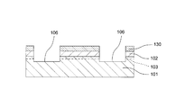
- FIG. 2 is a process cross-sectional view for explaining the method of manufacturing the nitride semiconductor device.
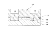
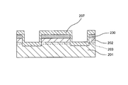
- FIG. 3 is a process cross-sectional view subsequent to FIG.
- FIG. 4 is a process cross-sectional view subsequent to FIG.
- FIG. 5 is a process cross-sectional view subsequent to FIG.
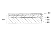
- FIG. 6 is a process sectional view for explaining the method for manufacturing a nitride semiconductor device according to the third embodiment of the present invention.
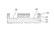
- FIG. 7 is a process cross-sectional view subsequent to FIG.
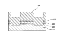
- FIG. 8 is a process cross-sectional view subsequent to FIG.
- FIG. 9 is a process cross-sectional view subsequent to FIG. FIG.
- FIG. 10 is a process cross-sectional view subsequent to FIG.
- FIG. 11 is a diagram showing the relationship between the oxygen concentration in the ohmic electrode and the contact resistance.
- FIG. 12 is a diagram showing the relationship between the annealing temperature of the ohmic electrode and the contact resistance.
- FIG. 1 shows a cross-sectional view of a nitride semiconductor device according to the first embodiment of the present invention, which is a GaN-based HFET (Hetero-junction Field Effect Transistor).
- a nitride semiconductor device according to the first embodiment of the present invention, which is a GaN-based HFET (Hetero-junction Field Effect Transistor).
- the semiconductor device includes an undoped AlGaN buffer layer 15, an undoped GaN layer 1 as an example of a first semiconductor layer, and an undoped AlGaN layer 2 as an example of a second semiconductor layer, on an Si substrate 10.
- a nitride semiconductor layer 20 made of is formed. 2DEG (two-dimensional electron gas) is generated at the interface between the undoped GaN layer 1 and the undoped AlGaN layer 2.
- a source electrode 11 and a drain electrode 12 are formed on the AlGaN layer 2 with a space therebetween.
- a gate electrode 13 is formed on the AlGaN layer 2 between the source electrode 11 and the drain electrode 12 and on the source electrode 11 side.
- the source electrode 11 and the drain electrode 12 are ohmic electrodes, and the gate electrode 13 is a Schottky electrode.
- the source electrode 11, the drain electrode 12, the gate electrode 13, and the active regions of the GaN layer 1 and the AlGaN layer 2 on which the source electrode 11, the drain electrode 12, and the gate electrode 13 are formed constitute an HFET.
- the active region means that carriers are generated between the source electrode 11 and the drain electrode 12 by the voltage applied to the gate electrode 13 disposed between the source electrode 11 and the drain electrode 12 on the AlGaN layer 2.
- This is a region of the flowing nitride semiconductor layer 20 (GaN layer 1, AlGaN layer 2).
- An insulating film 30 made of SiO 2 is formed on the AlGaN layer 2 excluding the region where the source electrode 11, the drain electrode 12, and the gate electrode 13 are formed in order to protect the AlGaN layer 2.
- An interlayer insulating film 40 made of polyimide is formed on the Si substrate 10 on which the source electrode 11, the drain electrode 12, and the gate electrode 13 are formed.
- reference numeral 41 denotes a via as a contact portion, and 42 denotes a drain electrode pad.
- the insulating film is not limited to SiO 2 but SiN, Al 2 O 3 or the like may be used.
- the insulating film preferably has a SiN film having a stoichiometric collapse on the surface of the semiconductor layer in order to suppress collapse and a multilayer structure of SiO 2 or SiN for surface protection.
- the interlayer insulating film is not limited to polyimide, but may be an insulating material such as SiO 2 film manufactured by p-CVD, SOG (Spin On Glass), or BPSG (boron / phosphorus / silicate / glass).
- a two-dimensional electron gas (2DEG) formed at the interface between the GaN layer 1 and the AlGaN layer 2 is generated to form a channel layer.
- the channel layer is controlled by applying a voltage to the gate electrode 13 to turn on and off the HFET having the source electrode 11, the drain electrode 12, and the gate electrode 13.
- a depletion layer is formed in the GaN layer 1 below the gate electrode 13, and the HFET is turned off.
- the HFET 13 is a normally-on type transistor in which the depletion layer disappears in the lower GaN layer 1 and is turned on.
- the Si substrate and the undoped AlGaN buffer layer are not shown in order to make the drawings easy to see, and the sizes and intervals of the source electrode and the drain electrode are changed.
- an undoped AlGaN buffer layer (not shown), undoped GaN is formed on a Si substrate (not shown) by using a MOCVD (Metal Organic Chemical Vapor Deposition) method.
- a layer 101 and an undoped AlGaN layer 102 are sequentially formed.
- the thickness of the undoped GaN layer 101 is 1 ⁇ m, for example, and the thickness of the undoped AlGaN layer 102 is 30 nm, for example.
- the GaN layer 101 and the AlGaN layer 102 constitute a nitride semiconductor layer 120.
- an insulating film 130 (for example, SiO 2 ) is formed to a thickness of 200 nm on the AlGaN layer 102 by, for example, a plasma CVD (Chemical Vapor Deposition) method.
- reference numeral 103 denotes a two-dimensional electron gas (2DEG) formed at the heterointerface between the GaN layer 101 and the AlGaN layer 102.
- a portion where an ohmic electrode is to be formed is removed by dry etching, and the GaN layer 101 penetrates the AlGaN layer 102.
- a recess 106 is formed in a part on the upper side of the substrate. The depth of the recess 106 may be equal to or greater than the depth from the surface of the AlGaN layer 102 to 2 DEG, for example, 50 nm.
- annealing is performed after dry etching (for example, 500 to 850 ° C.).
- Ti / Al / TiN is laminated on the insulating film 130 and the recess 106 by sputtering to form a laminated metal film 107 to be an ohmic electrode.
- the TiN layer is a cap layer for protecting the Ti / Al layer from the subsequent step.
- a small amount (for example, 5 sccm) of oxygen is allowed to flow into the chamber during Ti film formation.
- the flow rate of oxygen is set so that Ti oxide is not generated.
- patterns of ohmic electrodes 111 and 112 are formed by using normal photolithography and dry etching.
- annealing the substrate on which the ohmic electrodes 111 and 112 are formed for example, at 400 ° C. or more and 500 ° C. or less for 10 minutes or more, an ohmic contact is formed between the two-dimensional electron gas (2DEG) and the ohmic electrodes 111 and 112. can get.
- the contact resistance can be greatly reduced as compared with the case of annealing at a high temperature of 500 ° C. or higher.
- annealing at a low temperature of 400 ° C. or higher and 500 ° C. or lower does not adversely affect the characteristics of the insulating film.
- the ohmic electrodes 111 and 112 become a source electrode and a drain electrode, and a gate electrode made of TiN or WN is formed between the ohmic electrodes 111 and 112 in a later step.
- the nitride semiconductor device of the first embodiment when the laminated metal film 107 to be an ohmic electrode is formed, oxygen is flowed into the chamber during the Ti film formation, so that the ohmic contact can be achieved.
- the oxygen concentration in the ohmic electrodes 111 and 112 before annealing can be set to 1 ⁇ 10 16 cm ⁇ 3 or more and 1 ⁇ 10 20 cm ⁇ 3 or less. Thereby, the contact resistance between 2DEG of the nitride semiconductor layer after annealing and the ohmic electrodes 111 and 112 can be reduced.
- the oxygen concentration in the ohmic electrodes 111 and 112 is measured by SIMS (Secondary / Ion / Mass / Spectroscopy) before alloying by annealing.
- the oxygen concentration in the ohmic electrode made of a TiAl-based material affects the contact resistance in the course of various experiments conducted by the present inventor for a GaN-based HFET which is one of the nitride semiconductor devices.
- a GaN-based HFET which is one of the nitride semiconductor devices.
- 2DEG two-dimensional electron gas
- oxygen is contained in the Ti layer formed first on the AlGaN layer 102,
- the oxygen concentration in the ohmic electrode can be easily set to 1 ⁇ 10 16 cm ⁇ 3 or more and 1 ⁇ 10 20 cm ⁇ 3 or less.
- the insulating film 130, the AlGaN layer 102, and the GaN layer 101 are removed by dry etching to form the recess 106, but the insulating film 130 is removed by wet etching. Then, the recess 106 may be formed by removing the AlGaN layer 102 and the GaN layer 101 by dry etching.
- Ti / Al / TiN is laminated to form an ohmic electrode.
- the present invention is not limited to this, and TiN may be omitted, and Ti / Al is laminated. After that, Au, Ag, Pt or the like may be laminated thereon.
- the nitride semiconductor device of the second embodiment has the same configuration as the nitride semiconductor device of the first embodiment shown in FIG.
- the manufacturing method of the nitride semiconductor device according to the second embodiment is the same as that of the first embodiment except that oxygen is allowed to flow in the chamber before Ti deposition instead of oxygen to flow in the chamber during Ti deposition. It has the same steps as the method for manufacturing a nitride semiconductor device, and FIGS.
- the nitride semiconductor device when Ti / Al / TiN is laminated on the insulating film 130 and the recess 106 by sputtering to form the laminated metal film 107 serving as an ohmic electrode, a small amount of oxygen is introduced into the chamber during the Ti film formation.
- oxygen is flowed into the chamber, for example, at 50 sccm for 5 minutes before the Ti film is formed.
- the oxygen concentration can be set to 1 ⁇ 10 16 cm ⁇ 3 or more and 1 ⁇ 10 20 cm ⁇ 3 or less.
- the method for manufacturing a nitride semiconductor device according to the second embodiment has the same effects as the method for manufacturing a nitride semiconductor device according to the first embodiment.
- the laminated metal film 107 to be an ohmic electrode is formed by sputtering
- oxygen is allowed to flow in the chamber before Ti film formation to thereby form the ohmic electrode 111.
- 112 can be 1 ⁇ 10 16 cm ⁇ 3 or more and 1 ⁇ 10 20 cm ⁇ 3 or less. Thereby, the contact resistance between the 2DEG of the nitride semiconductor layer and the ohmic electrodes 111 and 112 can be reduced.
- FIG. 6 is a process sectional view for explaining the method for manufacturing a nitride semiconductor device according to the third embodiment of the invention.
- the nitride semiconductor device of the third embodiment has the same configuration as the nitride semiconductor device of the first embodiment shown in FIG.
- an undoped GaN layer 201 and an undoped AlGaN layer 202 are sequentially formed on a Si substrate (not shown) by MOCVD.
- the GaN layer 201 and the AlGaN layer 202 constitute a nitride semiconductor layer 220.
- an insulating film 230 (for example, SiO 2 ) is formed on the AlGaN layer 202.
- reference numeral 203 denotes a two-dimensional electron gas (2DEG) formed at the heterointerface between the GaN layer 201 and the AlGaN layer 202.
- the portion where the ohmic electrode is to be formed is removed by dry etching, thereby penetrating the AlGaN layer 202 and forming a GaN layer.
- a recess 206 is formed in a part of the upper side of 201.
- annealing is performed after dry etching (for example, 500 to 850 ° C.).
- a Ti layer 207 is formed on the insulating film 230 and in the recess 206 by sputtering.
- oxygen plasma treatment is performed on the surface of the Ti layer 207.
- This oxygen plasma treatment is desirably performed at 60 ° C., for example, with oxygen set at a flow rate of 900 sccm and RF power of 1000 W for 5 minutes.
- Al / TiN is laminated on the insulating film 230 and the concave portion 206 by sputtering to form a laminated metal film 208 to be an ohmic electrode.
- patterns of ohmic electrodes 211 and 212 are formed by using normal photolithography and dry etching.
- the method for manufacturing a nitride semiconductor device according to the third embodiment has the same effect as the method for manufacturing a nitride semiconductor device according to the first embodiment.
- the oxygen plasma treatment is performed on the surface of the Ti layer after the Ti layer is sputtered.
- the oxygen concentration in the ohmic electrodes 211 and 212 can be set to 1 ⁇ 10 16 cm ⁇ 3 or more and 1 ⁇ 10 20 cm ⁇ 3 or less.
- the contact resistance between the 2DEG of the nitride semiconductor layer and the ohmic electrodes 211 and 212 can be reduced.
- FIG. 11 is a diagram showing the relationship between the oxygen concentration in the ohmic electrode of the nitride semiconductor device and the contact resistance.
- the oxygen concentration in the ohmic electrode before annealing is measured by SIMS.
- the oxygen concentration may be measured using other measurement methods such as AES (AtomicAtEmission Spectroscopy).
- the contact resistance (vertical axis) in FIG. 11 is obtained by measuring the contact resistance of the ohmic electrode after annealing.
- the nitride semiconductor device having a contact resistance of 6 ⁇ mm or less is realized by setting the oxygen concentration in the ohmic electrode to 1 ⁇ 10 16 cm ⁇ 3 or more and 1 ⁇ 10 20 cm ⁇ 3 or less. be able to.
- the music point has never been known.
- Such a nitride semiconductor device having a contact resistance of 6 ⁇ mm or less has a commercial value in terms of performance and cost as a product that can be driven with a larger current than a silicon element and is suitable for high-temperature operation.
- FIG. 12 is a diagram showing the relationship between the annealing temperature and contact resistance of an ohmic electrode manufactured using the method for manufacturing a nitride semiconductor device shown in the first embodiment.
- the contact resistance between the nitride semiconductor layer and the ohmic electrode can be significantly reduced by annealing at a temperature of 400 ° C. or more and 500 ° C. or less.
- the annealing temperature of n-type GaN is 600 ° C. and the annealing temperature of non-doped GaN is 800 ° C.
- an ohmic electrode is formed in the annealing step.
- the nitride semiconductor device using the Si substrate has been described.
- the present invention is not limited to the Si substrate, and a sapphire substrate or SiC substrate may be used, and nitriding is performed on the sapphire substrate or SiC substrate.
- a nitride semiconductor layer may be grown on a substrate made of a nitride semiconductor, such as growing an AlGaN layer on a GaN substrate.
- a buffer layer may be formed between the substrate and the nitride semiconductor layer, or a hetero improvement layer is formed between the first semiconductor layer, the first semiconductor layer, and the second semiconductor layer of the nitride semiconductor layer. May be.
- the HFET having the recess structure in which the ohmic electrode reaches the GaN layer has been described.
- the ohmic electrode serving as the source electrode and the drain electrode is formed on the undoped AlGaN layer without forming the recess.
- the present invention may be applied to the formed HFET.
- the nitride semiconductor device of the present invention is not limited to an HFET that uses 2DEG, and the same effect can be obtained even with field effect transistors having other configurations.
- the normally-on type HFET has been described.
- the present invention may be applied to a normally-off type nitride semiconductor device.
- the present invention may be applied not only to a Schottky electrode but also to a field effect transistor having an insulated gate structure.
- the nitride semiconductor of the nitride semiconductor device of the present invention may be any material represented by Al x In y Ga 1-xy N (x ⁇ 0, y ⁇ 0, 0 ⁇ x + y ⁇ 1).
Landscapes
- Electrodes Of Semiconductors (AREA)
- Junction Field-Effect Transistors (AREA)
- Physical Vapour Deposition (AREA)
Abstract
Si基板(10)上に形成されたアンドープGaN層(1),アンドープAlGaN層(2)と、アンドープGaN層(1),アンドープAlGaN層(2)上に形成されたTi/Al/TiNからなるオーミック電極(ソース電極(11),ドレイン電極(12))とを備える。上記オーミック電極中の酸素濃度を1×1016cm-3以上かつ1×1020cm-3以下とする。これにより、窒化物半導体層とオーミック電極とのコンタクト抵抗を低減できる窒化物半導体装置を提供する。
Description
この発明は、窒化物半導体装置およびその製造方法に関する。
従来、窒化物半導体装置としては、n型GaNコンタクト層の表面に酸素プラズマ処理を行って酸素ドープ層を形成した後に、そのn型GaNコンタクト層上にオーミック電極を形成することによって、n型GaNコンタクト層とオーミック電極とのコンタクト抵抗を低減するものがある(例えば、特許第2967743号(特許文献1)参照)。
ところが、上記窒化物半導体装置について、本発明者が実際に実験を行ってGaN層に酸素プラズマ処理を行った後にオーミック電極を形成した場合、オーミック電極のコンタクト抵抗が高く、十分に低いコンタクト抵抗を得ることはどうしてもできなかった。
そこで、この発明の課題は、窒化物半導体層とオーミック電極とのコンタクト抵抗を低減できる窒化物半導体装置およびその製造方法を提供することにある。
本発明者は、上記従来の窒化物半導体装置のようにGaN層側に酸素をドープさせることなく、窒化物半導体層上に形成されたオーミック電極のコンタクト抵抗について鋭意検討した結果、TiAl系材料からなるオーミック電極中に酸化物ができない程度の酸素原子を不純物として含有させたとき、オーミック電極中の酸素濃度に応じて窒化物半導体層とオーミック電極とのコンタクト抵抗の特性が変化することを発見した。
本発明は、このような本発明者の発見に基づいて、オーミック電極中の酸素濃度が特定の範囲内であるときにコンタクト抵抗が大幅に減少することを実験により初めて見出したものである。
すなわち、第1の発明の窒化物半導体装置は、
基板と、
上記基板上に形成された窒化物半導体層と、
上記窒化物半導体層上に形成されたTiAl系材料からなるオーミック電極と
を備え、
上記TiAl系材料からなるオーミック電極中の酸素濃度が1×1016cm-3以上かつ1×1020cm-3以下であることを特徴とする。
基板と、
上記基板上に形成された窒化物半導体層と、
上記窒化物半導体層上に形成されたTiAl系材料からなるオーミック電極と
を備え、
上記TiAl系材料からなるオーミック電極中の酸素濃度が1×1016cm-3以上かつ1×1020cm-3以下であることを特徴とする。
ここで、上記窒化物半導体装置の窒化物半導体は、AlxInyGa1-x-yN(x≦0、y≦0、0≦x+y≦1)で表されるものであればよい。また、TiAl系材料としては、少なくともTi/Alからなり、その上にTiNのキャップ層を積層してもよいし、Alの上にAu,Ag,Ptなどを積層してもよい。
上記構成によれば、TiAl系材料からなるオーミック電極中の酸素濃度を1×1016cm-3以上かつ1×1020cm-3以下とすることによって、窒化物半導体層とオーミック電極とのコンタクト抵抗を低減できる。
また、一実施形態の窒化物半導体装置では、
上記窒化物半導体層は、上記基板上に順に積層された第1半導体層およびその第1半導体層とヘテロ界面を形成する第2半導体層を含み、
上記第1半導体層と上記第2半導体層とのヘテロ界面に2次元電子ガスが形成され、
上記第2半導体層を貫通して上記第1半導体層の上側の一部に凹部が形成され、上記凹部に上記オーミック電極の少なくとも一部が埋め込まれている。
上記窒化物半導体層は、上記基板上に順に積層された第1半導体層およびその第1半導体層とヘテロ界面を形成する第2半導体層を含み、
上記第1半導体層と上記第2半導体層とのヘテロ界面に2次元電子ガスが形成され、
上記第2半導体層を貫通して上記第1半導体層の上側の一部に凹部が形成され、上記凹部に上記オーミック電極の少なくとも一部が埋め込まれている。
上記実施形態によれば、第2半導体層を貫通して第1半導体層の上側の一部に形成された凹部に、オーミック電極の少なくとも一部が埋め込まれたリセス構造の窒化物半導体装置において、第1半導体層と第2半導体層とのヘテロ界面の2次元電子ガスとオーミック電極とのコンタクト抵抗を低減できる。
また、一実施形態の窒化物半導体装置では、
上記TiAl系材料からなるオーミック電極は、少なくともTi層とAl層とが上記基板側から順に積層された積層金属膜である。
上記TiAl系材料からなるオーミック電極は、少なくともTi層とAl層とが上記基板側から順に積層された積層金属膜である。
上記実施形態によれば、少なくともTi層とAl層とが基板側から順に積層された積層金属膜であるオーミック電極を用いて、製造時にTi層に酸素を含ませる工程によって、オーミック電極中の酸素濃度を1×1016cm-3以上かつ1×1020cm-3以下にすることが容易にできる。
また、第2の発明の窒化物半導体装置の製造方法では、
基板上に窒化物半導体層を形成するステップと、
上記窒化物半導体層上にTiAl系材料からなる金属膜をスパッタリングにより形成するステップと、
上記TiAl系材料からなる金属膜をエッチングしてオーミック電極を形成するステップと、
上記オーミック電極が形成された上記基板に対してアニールを行うステップと
を含み、
上記TiAl系材料からなる金属膜を形成するステップにおいて、上記TiAl系材料からなる金属膜のうちのTi層のスパッタリング中にチャンバー内に酸素を流すことによって、上記オーミック電極中の酸素濃度を1×1016cm-3以上かつ1×1020cm-3以下にすることを特徴とする。
基板上に窒化物半導体層を形成するステップと、
上記窒化物半導体層上にTiAl系材料からなる金属膜をスパッタリングにより形成するステップと、
上記TiAl系材料からなる金属膜をエッチングしてオーミック電極を形成するステップと、
上記オーミック電極が形成された上記基板に対してアニールを行うステップと
を含み、
上記TiAl系材料からなる金属膜を形成するステップにおいて、上記TiAl系材料からなる金属膜のうちのTi層のスパッタリング中にチャンバー内に酸素を流すことによって、上記オーミック電極中の酸素濃度を1×1016cm-3以上かつ1×1020cm-3以下にすることを特徴とする。
上記構成によれば、TiAl系材料からなる金属膜を形成するステップにおいて、TiAl系材料からなる金属膜のうちのTi層のスパッタリング中にチャンバー内に酸素を流して、オーミック電極中の酸素濃度を1×1016cm-3以上かつ1×1020cm-3以下とすることによって、窒化物半導体層とオーミック電極とのコンタクト抵抗を低減できる。
また、第3の発明の窒化物半導体装置の製造方法では
基板上に窒化物半導体層を形成するステップと、
上記窒化物半導体層上にTiAl系材料からなる金属膜をスパッタリングにより形成するステップと、
上記TiAl系材料からなる金属膜をエッチングしてオーミック電極を形成するステップと、
上記オーミック電極が形成された上記基板に対してアニールを行うステップと
を含み、
上記TiAl系材料からなる金属膜を形成するステップにおいて、上記TiAl系材料からなる金属膜のうちのTi層のスパッタリングの前にチャンバー内に酸素を流すことによって、上記オーミック電極中の酸素濃度を1×1016cm-3以上かつ1×1020cm-3以下にすることを特徴とする。
基板上に窒化物半導体層を形成するステップと、
上記窒化物半導体層上にTiAl系材料からなる金属膜をスパッタリングにより形成するステップと、
上記TiAl系材料からなる金属膜をエッチングしてオーミック電極を形成するステップと、
上記オーミック電極が形成された上記基板に対してアニールを行うステップと
を含み、
上記TiAl系材料からなる金属膜を形成するステップにおいて、上記TiAl系材料からなる金属膜のうちのTi層のスパッタリングの前にチャンバー内に酸素を流すことによって、上記オーミック電極中の酸素濃度を1×1016cm-3以上かつ1×1020cm-3以下にすることを特徴とする。
上記構成によれば、TiAl系材料からなる金属膜を形成するステップにおいて、TiAl系材料からなる金属膜のうちのTi層のスパッタリングの前にチャンバー内に酸素を流して、オーミック電極中の酸素濃度を1×1016cm-3以上かつ1×1020cm-3以下とすることによって、窒化物半導体層とオーミック電極とのコンタクト抵抗を低減できる。
また、第4の発明の窒化物半導体装置の製造方法では
基板上に窒化物半導体層を形成するステップと、
上記窒化物半導体層上にTiAl系材料からなる金属膜をスパッタリングにより形成するステップと、
上記TiAl系材料からなる金属膜をエッチングしてオーミック電極を形成するステップと、
上記オーミック電極が形成された上記基板に対してアニールを行うステップと
を含み、
上記TiAl系材料からなる金属膜をスパッタリングにより形成するステップの後、かつ、上記オーミック電極を形成するステップの前に、上記TiAl系材料からなる金属膜のうちのTi層のスパッタリング後にそのTi層の表面に対して酸素プラズマ処理を行うことによって、上記オーミック電極中の酸素濃度を1×1016cm-3以上かつ1×1020cm-3以下にすることを特徴とする。
基板上に窒化物半導体層を形成するステップと、
上記窒化物半導体層上にTiAl系材料からなる金属膜をスパッタリングにより形成するステップと、
上記TiAl系材料からなる金属膜をエッチングしてオーミック電極を形成するステップと、
上記オーミック電極が形成された上記基板に対してアニールを行うステップと
を含み、
上記TiAl系材料からなる金属膜をスパッタリングにより形成するステップの後、かつ、上記オーミック電極を形成するステップの前に、上記TiAl系材料からなる金属膜のうちのTi層のスパッタリング後にそのTi層の表面に対して酸素プラズマ処理を行うことによって、上記オーミック電極中の酸素濃度を1×1016cm-3以上かつ1×1020cm-3以下にすることを特徴とする。
上記構成によれば、TiAl系材料からなる金属膜をスパッタリングにより形成するステップの後、かつ、オーミック電極を形成するステップの前に、TiAl系材料からなる金属膜のうちのTi層のスパッタリング後にそのTi層の表面に対して酸素プラズマ処理を行って、オーミック電極中の酸素濃度を1×1016cm-3以上かつ1×1020cm-3以下とすることによって、窒化物半導体層とオーミック電極とのコンタクト抵抗を低減できる。
また、一実施形態の窒化物半導体装置の製造方法では
上記第1~第3の発明の窒化物半導体装置の製造方法において、
上記窒化物半導体層は、上記基板上に順に積層された第1半導体層およびその第1半導体層とヘテロ界面を形成する第2半導体層を含み、
上記窒化物半導体層を形成した後、かつ、上記TiAl系材料からなる金属膜をスパッタリングにより形成する前に、エッチングにより上記第2半導体層を貫通して上記第1半導体層の上側の一部に凹部を形成するステップを含み、
上記第1半導体層と上記第2半導体層とのヘテロ界面に2次元電子ガスが形成されると共に、
上記オーミック電極を形成するステップにおいて、上記TiAl系材料からなる金属膜をエッチングして上記凹部に少なくとも一部が埋め込まれた上記オーミック電極を形成する。
上記第1~第3の発明の窒化物半導体装置の製造方法において、
上記窒化物半導体層は、上記基板上に順に積層された第1半導体層およびその第1半導体層とヘテロ界面を形成する第2半導体層を含み、
上記窒化物半導体層を形成した後、かつ、上記TiAl系材料からなる金属膜をスパッタリングにより形成する前に、エッチングにより上記第2半導体層を貫通して上記第1半導体層の上側の一部に凹部を形成するステップを含み、
上記第1半導体層と上記第2半導体層とのヘテロ界面に2次元電子ガスが形成されると共に、
上記オーミック電極を形成するステップにおいて、上記TiAl系材料からなる金属膜をエッチングして上記凹部に少なくとも一部が埋め込まれた上記オーミック電極を形成する。
上記実施形態によれば、エッチングにより第2半導体層を貫通して第1半導体層の上側の一部に形成された凹部に、オーミック電極の少なくとも一部が埋め込まれたリセス構造の窒化物半導体装置において、第1半導体層と第2半導体層とのヘテロ界面の2次元電子ガスとオーミック電極とのコンタクト抵抗を低減できる。
また、一実施形態の窒化物半導体装置の製造方法では
上記アニールを行うステップにおいて、上記オーミック電極が形成された上記基板を400℃以上かつ500℃以下で加熱する。
上記アニールを行うステップにおいて、上記オーミック電極が形成された上記基板を400℃以上かつ500℃以下で加熱する。
上記実施形態によれば、アニールを行うステップにおいて、オーミック電極が形成された基板を400℃以上かつ500℃以下で加熱することによって、500℃以上の高温でアニールした場合に比べて、窒化物半導体層とオーミック電極とのコンタクト抵抗を大幅に低減できる。
以上より明らかなように、この発明の窒化物半導体装置およびその製造方法によれば、GaN系半導体層とオーミック電極とのコンタクト抵抗を低減できる窒化物半導体装置を実現することができる。
以下、この発明の窒化物半導体装置およびその製造方法を図示の実施の形態により詳細に説明する。
〔第1実施形態〕
図1はこの発明の第1実施形態の窒化物半導体装置の断面図を示しており、この窒化物半導体装置はGaN系HFET(Hetero-junction Field Effect Transistor;ヘテロ接合電界効果トランジスタ)である。
図1はこの発明の第1実施形態の窒化物半導体装置の断面図を示しており、この窒化物半導体装置はGaN系HFET(Hetero-junction Field Effect Transistor;ヘテロ接合電界効果トランジスタ)である。
この半導体装置は、図1に示すように、Si基板10上に、アンドープAlGaNバッファ層15、第1半導体層の一例としてのアンドープGaN層1と、第2半導体層の一例としてのアンドープAlGaN層2からなる窒化物半導体層20を形成している。このアンドープGaN層1とアンドープAlGaN層2との界面に2DEG(2次元電子ガス)が発生する。
また、AlGaN層2上に、互いに間隔をあけてソース電極11とドレイン電極12とを形成している。また、AlGaN層2上に、ソース電極11とドレイン電極12との間かつソース電極11側にゲート電極13を形成している。ソース電極11とドレイン電極12はオーミック電極であり、ゲート電極13はショットキー電極である。上記ソース電極11と、ドレイン電極12と、ゲート電極13と、そのソース電極11,ドレイン電極12,ゲート電極13が形成されたGaN層1,AlGaN層2の活性領域でHFETを構成している。
ここで、活性領域とは、AlGaN層2上のソース電極11とドレイン電極12との間に配置されたゲート電極13に印加される電圧によって、ソース電極11とドレイン電極12との間でキャリアが流れる窒化物半導体層20(GaN層1,AlGaN層2)の領域である。
そして、ソース電極11とドレイン電極12とゲート電極13が形成された領域を除くAlGaN層2上に、AlGaN層2を保護するため、SiO2からなる絶縁膜30を形成している。また、ソース電極11とドレイン電極12とゲート電極13とが形成されたSi基板10上に、ポリイミドからなる層間絶縁膜40を形成している。また、図1において、41はコンタクト部としてのビア、42はドレイン電極パッドである。なお、絶縁膜は、SiO2に限らず、SiNやAl2O3などを用いてもよい。特に、絶縁膜として、コラプス抑制のために半導体層表面にストイキオメトリックを崩したSiN膜と表面保護のためのSiO2やSiNの多層膜構造とするのが好ましい。また、層間絶縁膜は、ポリイミドに限らず、p-CVDで製造したSiO2膜やSOG(Spin On Glass)やBPSG(ホウ素・リン・シリケート・ガラス)などの絶縁材料を用いてもよい。
上記構成の窒化物半導体装置において、GaN層1とAlGaN層2との界面に形成された2次元電子ガス(2DEG)が発生してチャネル層が形成される。このチャネル層をゲート電極13に電圧を印加することにより制御して、ソース電極11とドレイン電極12とゲート電極13を有するHFETをオンオフさせる。このHFETは、ゲート電極13に負電圧が印加されているときにゲート電極13下のGaN層1に空乏層が形成されてオフ状態となる一方、ゲート電極13の電圧がゼロのときにゲート電極13下のGaN層1に空乏層がなくなってオン状態となるノーマリーオンタイプのトランジスタである。
次に、上記窒化物半導体装置の製造方法を図2~図6に従って説明する。なお、図2~図6では、図を見やすくするためにSi基板やアンドープAlGaNバッファ層を図示せず、また、ソース電極とドレイン電極の大きさや間隔を変えている。
まず、図2に示すように、Si基板(図示せず)上に、MOCVD(Metal Organic Chemical Vapor Deposition:有機金属気相成長)法を用いて、アンドープAlGaNバッファ層(図示せず)、アンドープGaN層101とアンドープAlGaN層102を順に形成する。アンドープGaN層101の厚さは例えば1μm、アンドープAlGaN層102の厚さは例えば30nmとする。このGaN層101とAlGaN層102が窒化物半導体層120を構成している。次に、AlGaN層102上に絶縁膜130(例えばSiO2)を例えばプラズマCVD(Chemical Vapor Deposition:化学的気相成長))法により200nm成膜する。図2において、103は、GaN層101とAlGaN層102とのヘテロ界面に形成される2次元電子ガス(2DEG)である。
次に、図3に示すように、絶縁膜130上にフォトレジストを塗布してパターニングした後、ドライエッチングによりオーミック電極を形成すべき部分を除去して、AlGaN層102を貫通してGaN層101の上側の一部に凹部106を形成する。凹部106の深さはAlGaN層102の表面から2DEGまでの深さ以上であればよく、例えば50nmとする。そして、ドライエッチング後にアニールを行う(例えば500~850℃)。
次に、図4に示すように、絶縁膜130上および凹部106にスパッタリングによりTi/Al/TiNを積層して、オーミック電極となる積層金属膜107を形成する。ここで、TiN層は、後工程からTi/Al層を保護するためのキャップ層である。
このとき、Ti成膜中に少量(例えば5sccm)の酸素をチャンバー内に流す。ここで、酸素の流量は、Tiの酸化物が生成されない量とする。
次に、図5に示すように、通常のフォトリソグラフィおよびドライエッチングを用いて、オーミック電極111,112のパターンを形成する。
そして、オーミック電極111,112が形成された基板を例えば400℃以上かつ500℃以下で10分以上アニールすることによって、2次元電子ガス(2DEG)とオーミック電極111,112との間にオーミックコンタクトが得られる。この場合、500℃以上の高温でアニールした場合に比べてコンタクト抵抗を大幅に低減できる。また、400℃以上かつ500℃以下の低温でアニールすることにより絶縁膜の特性に悪影響を与えることがない。
このオーミック電極111,112がソース電極とドレイン電極となり、後の工程でオーミック電極111,112の間にTiNまたはWNなどからなるゲート電極が形成される。
上記第1実施形態の窒化物半導体装置の製造方法によれば、オーミック電極となる積層金属膜107を形成するときに、Ti成膜中に酸素をチャンバー内に流すことによって、オーミックコンタクトのためのアニール前のオーミック電極111,112中の酸素濃度を1×1016cm-3以上かつ1×1020cm-3以下にすることが可能となる。これによって、アニール後の窒化物半導体層の2DEGとオーミック電極111,112とのコンタクト抵抗を低減できる。
なお、オーミック電極111,112中の酸素濃度は、SIMS(Secondary Ion Mass Spectroscopy:二次イオン質量分析法)によりアニールによる合金化の前に測定している。
本発明は、窒化物半導体装置の1つであるGaN系HFETについて本発明者が行った様々な実験の過程で、TiAl系材料からなるオーミック電極中の酸素濃度がコンタクト抵抗に影響することを偶然見出し、その影響について研究した結果によるものであるが、その具体的な原理については未だ不明である。
また、AlGaN層102を貫通してGaN層101の上側の一部に凹部106にオーミック電極111,112の一部が埋め込まれたリセス構造の窒化物半導体装置において、GaN層101とAlGaN層102とのヘテロ界面の2次元電子ガス(2DEG)とオーミック電極111,112とのコンタクト抵抗を低減できる。
また、Ti層とAl層とが基板側から順に積層された積層金属膜であるオーミック電極111,112を用いて、AlGaN層102上に最初に形成されるTi層に酸素を含ませることによって、オーミック電極中の酸素濃度を1×1016cm-3以上かつ1×1020cm-3以下にすることが容易にできる。
上記第1実施形態の窒化物半導体装置の製造方法によれば、絶縁膜130、AlGaN層102、GaN層101をドライエッチングにより除去し、凹部106を形成したが、絶縁膜130をウェットエッチングにより除去し、その後AlGaN層102、GaN層101をドライエッチングにより除去することにより、凹部106を形成してもよい。
上記第1実施形態の窒化物半導体装置の製造方法によれば、Ti/Al/TiNを積層してオーミック電極としたが、これに限らず、TiNはなくともよく、また、Ti/Alを積層した後、その上にAu,Ag,Ptなどを積層してもよい。
〔第2実施形態〕
次に、この発明の第2実施形態の窒化物半導体装置の製造方法を説明する。この第2実施形態の窒化物半導体装置は、図1に示す第1実施形態の窒化物半導体装置と同一の構成をしている。また、この第2実施形態の窒化物半導体装置の製造方法は、Ti成膜中にチャンバー内に酸素を流す代わりにTi成膜前にチャンバー内に酸素を流すことを除いて第1実施形態の窒化物半導体装置の製造方法と同一の工程を有し、図2~図5を援用する。
次に、この発明の第2実施形態の窒化物半導体装置の製造方法を説明する。この第2実施形態の窒化物半導体装置は、図1に示す第1実施形態の窒化物半導体装置と同一の構成をしている。また、この第2実施形態の窒化物半導体装置の製造方法は、Ti成膜中にチャンバー内に酸素を流す代わりにTi成膜前にチャンバー内に酸素を流すことを除いて第1実施形態の窒化物半導体装置の製造方法と同一の工程を有し、図2~図5を援用する。
以下、第1実施形態の窒化物半導体装置の製造方法と異なる点について説明する。
第1実施形態において、絶縁膜130上および凹部106にスパッタリングによりTi/Al/TiNを積層して、オーミック電極となる積層金属膜107を形成するときに、Ti成膜中に少量の酸素をチャンバー内に流したのに対して、この第2実施形態の窒化物半導体装置の製造方法では、Ti成膜前にチャンバー内に酸素を例えば50sccm、5分間流すことによって、オーミック電極111,112中の酸素濃度を1×1016cm-3以上かつ1×1020cm-3以下にすることが可能となる。
上記第2実施形態の窒化物半導体装置の製造方法は、第1実施形態の窒化物半導体装置の製造方法と同様の効果を有する。
上記第2実施形態の窒化物半導体装置の製造方法によれば、オーミック電極となる積層金属膜107をスパッタリングにより形成するときに、Ti成膜前にチャンバー内に酸素を流すことによって、オーミック電極111,112中の酸素濃度を1×1016cm-3以上かつ1×1020cm-3以下にすることが可能となる。これによって、窒化物半導体層の2DEGとオーミック電極111,112とのコンタクト抵抗を低減できる。
〔第3実施形態〕
図6はこの発明の第3実施形態の窒化物半導体装置の製造方法を説明するための工程断面図を示している。この第3実施形態の窒化物半導体装置は、図1に示す第1実施形態の窒化物半導体装置と同一の構成をしている。
図6はこの発明の第3実施形態の窒化物半導体装置の製造方法を説明するための工程断面図を示している。この第3実施形態の窒化物半導体装置は、図1に示す第1実施形態の窒化物半導体装置と同一の構成をしている。
まず、図6に示すように、Si基板(図示せず)上に、MOCVD法を用いて、アンドープGaN層201とアンドープAlGaN層202を順に形成する。このGaN層201とAlGaN層202が窒化物半導体層220を構成している。次に、AlGaN層202上に絶縁膜230(例えばSiO2)を成膜する。図6において、203は、GaN層201とAlGaN層202とのヘテロ界面に形成される2次元電子ガス(2DEG)である。
次に、図7に示すように、絶縁膜230上にフォトレジストを塗布してパターニングした後、ドライエッチングによりオーミック電極を形成すべき部分を除去することによって、AlGaN層202を貫通してGaN層201の上側の一部に凹部206を形成する。そして、ドライエッチング後にアニールを行う(例えば500~850℃)。
次に、図8に示すように、絶縁膜230上および凹部206にスパッタリングによりTi層207を形成する。
次に、Ti層207表面に酸素プラズマ処理を行う。この酸素プラズマ処理は、例えば60℃において、酸素を900sccmの流量に設定し、RFパワー1000Wにて5分間行うことが望ましい。
次に、図9に示すように、絶縁膜230上および凹部206にスパッタリングによりAl/TiNを積層して、オーミック電極となる積層金属膜208を形成する。
次に、図10に示すように、通常のフォトリソグラフィおよびドライエッチングを用いて、オーミック電極211,212のパターンを形成する。
そして、オーミック電極211,212が形成された基板を例えば400℃以上かつ500℃以下で10分以上アニールすることによって、2DEGとオーミック電極211,212との間にオーミックコンタクトが得られる。
上記第3実施形態の窒化物半導体装置の製造方法は、第1実施形態の窒化物半導体装置の製造方法と同様の効果を有する。
上記第3実施形態の窒化物半導体装置の製造方法によれば、オーミック電極となる積層金属膜107を形成するときに、Ti層のスパッタリング後にそのTi層の表面に対して酸素プラズマ処理を行うことによって、オーミック電極211,212中の酸素濃度を1×1016cm-3以上かつ1×1020cm-3以下にすることが可能となる。これによって、窒化物半導体層の2DEGとオーミック電極211,212とのコンタクト抵抗を低減できる。
図11は上記窒化物半導体装置のオーミック電極中の酸素濃度とコンタクト抵抗との関係を示す図である。
ただし、図11の酸素濃度(横軸)は、アニールする前のオーミック電極中の酸素濃度をSIMSにより測定している。なお、酸素濃度の測定は、AES(Atomic Emission Spectroscopy:オージェ電子分光法)などの他の測定方法を用いて行ってもよい。
一方、図11のコンタクト抵抗(縦軸)は、アニールした後のオーミック電極のコンタクト抵抗を測定したものである。
図11から明らかなように、オーミック電極中の酸素濃度を1×1016cm-3以上かつ1×1020cm-3以下とすることで、コンタクト抵抗が6Ωmm以下の窒化物半導体装置を実現することができる。特に、オーミック電極中の酸素濃度が1×1020cm-3を越えたところにコンタクト抵抗が急激に増大する変曲点が存在し、このオーミック電極中の酸素濃度に依存したコンタクト抵抗特性の変曲点はこれまで全く知られていなかった。
このようなコンタクト抵抗が6Ωmm以下の窒化物半導体装置は、シリコン素子よりも大電流駆動が可能でかつ高温動作に適した製品として性能面およびコスト面で商業的価値を有する。
また、図12は第1実施形態に示す窒化物半導体装置の製造方法を用いて作製したオーミック電極のアニール温度とコンタクト抵抗との関係を表す図である。
このとき、Ti成膜中に5sccmの酸素をチャンバー内に流しながらスパッタリングを行い、アニールする前のオーミック電極中の酸素濃度をSIMSにより測定したところ、2×1019cm-3であった。
このように、400℃以上かつ500℃以下の温度でアニールすることによって、窒化物半導体層とオーミック電極とのコンタクト抵抗を大幅に低減できることがわかる。
通常、n型GaNのアニール温度が600℃、ノンドープGaNのアニール温度が800℃で行われるのに対して、この窒化物半導体装置の製造方法では、アニールを行うステップにおいて、オーミック電極が形成された基板を400℃以上かつ500℃以下の低い温度で加熱することによって、アニール温度が400℃より低温かまたは500℃より高温の場合に比べて、窒化物半導体層とオーミック電極とのコンタクト抵抗を大幅に低減することができる。
上記第1~第3実施の形態では、Si基板を用いた窒化物半導体装置について説明したが、Si基板に限らず、サファイヤ基板やSiC基板を用いてもよく、サファイヤ基板やSiC基板上に窒化物半導体層を成長させてもよいし、GaN基板にAlGaN層を成長させる等のように、窒化物半導体からなる基板上に窒化物半導体層を成長させてもよい。また、基板と窒化物半導体層との間にバッファ層を形成してもよいし、窒化物半導体層の第1半導体層と第1半導体層と第2半導体層との間にヘテロ改善層を形成してもよい。
また、上記第1~第3実施の形態では、オーミック電極がGaN層に達するリセス構造のHFETについて説明したが、リセスを形成せずにアンドープAlGaN層上にソース電極およびドレイン電極となるオーミック電極を形成したHFETにこの発明を適用してもよい。また、この発明の窒化物半導体装置は、2DEGを利用するHFETに限らず、他の構成の電界効果トランジスタであっても同様の効果が得られる。
また、上記第1~第3実施の形態では、ノーマリーオンタイプのHFETについて説明したが、ノーマリーオフタイプの窒化物半導体装置にこの発明を適用してもよい。また、ショットキー電極に限らず、絶縁ゲート構造の電界効果トランジスタにこの発明を適用してもよい。
この発明の窒化物半導体装置の窒化物半導体は、AlxInyGa1-x-yN(x≦0、y≦0、0≦x+y≦1)で表されるものであればよい。
この発明の具体的な実施の形態について説明したが、この発明は上記第1~第3実施形態に限定されるものではなく、この発明の範囲内で種々変更して実施することができる。
1,101,201……GaN層
2,102,202…AlGaN層
3,103,203…2DEG
10…Si基板
11…ソース電極
12…ドレイン電極
13…ゲート電極
15…AlGaNバッファ層
20,120,220…窒化物半導体層
30,130,230…絶縁膜
40…層間絶縁膜
41…ビア
42…ドレイン電極パッド
111,211,112,212…オーミック電極
2,102,202…AlGaN層
3,103,203…2DEG
10…Si基板
11…ソース電極
12…ドレイン電極
13…ゲート電極
15…AlGaNバッファ層
20,120,220…窒化物半導体層
30,130,230…絶縁膜
40…層間絶縁膜
41…ビア
42…ドレイン電極パッド
111,211,112,212…オーミック電極
Claims (8)
- 基板と、
上記基板上に形成された窒化物半導体層(20,120,220)と、
上記窒化物半導体層(20,120,220)上に形成されたTiAl系材料からなるオーミック電極(11,12,111,112,211,212)と
を備え、
上記TiAl系材料からなるオーミック電極(11,12,111,112,211,212)中の酸素濃度が1×1016cm-3以上かつ1×1020cm-3以下であることを特徴とする窒化物半導体装置。 - 請求項1に記載の窒化物半導体装置において、
上記窒化物半導体層(20,120,220)は、上記基板上に順に積層された第1半導体層(1,101,201)およびその第1半導体層(1,101,201)とヘテロ界面を形成する第2半導体層(2,102,202)を含み、
上記第1半導体層(1,101,201)と上記第2半導体層(2,102,202)とのヘテロ界面に2次元電子ガスが形成され、
上記第2半導体層(2,102,202)を貫通して上記第1半導体層(1,101,201)の上側の一部に凹部が形成され、上記凹部に上記オーミック電極(11,12,111,112,211,212)の少なくとも一部が埋め込まれていることを特徴とする窒化物半導体装置。 - 請求項1または2に記載の窒化物半導体装置において、
上記TiAl系材料からなるオーミック電極(111,211,112,212)は、少なくともTi層とAl層とが上記基板側から順に積層された積層金属膜であることを特徴とする窒化物半導体装置。 - 基板上に窒化物半導体層(120)を形成するステップと、
上記窒化物半導体層(120)上にTiAl系材料からなる金属膜をスパッタリングにより形成するステップと、
上記TiAl系材料からなる金属膜をエッチングしてオーミック電極(111,112)を形成するステップと、
上記オーミック電極(111,112)が形成された上記基板に対してアニールを行うステップと
を含み、
上記TiAl系材料からなる金属膜を形成するステップにおいて、上記TiAl系材料からなる金属膜のうちのTi層のスパッタリング中にチャンバー内に酸素を流すことによって、上記オーミック電極(111,112)中の酸素濃度を1×1016cm-3以上かつ1×1020cm-3以下にすることを特徴とする窒化物半導体装置の製造方法。 - 基板上に窒化物半導体層(120)を形成するステップと、
上記窒化物半導体層(120)上にTiAl系材料からなる金属膜をスパッタリングにより形成するステップと、
上記TiAl系材料からなる金属膜をエッチングしてオーミック電極(111,112)を形成するステップと、
上記オーミック電極(111,112)が形成された上記基板に対してアニールを行うステップと
を含み、
上記TiAl系材料からなる金属膜を形成するステップにおいて、上記TiAl系材料からなる金属膜のうちのTi層のスパッタリングの前にチャンバー内に酸素を流すことによって、上記オーミック電極(111,112)中の酸素濃度を1×1016cm-3以上かつ1×1020cm-3以下にすることを特徴とする窒化物半導体装置の製造方法。 - 基板上に窒化物半導体層(220)を形成するステップと、
上記窒化物半導体層(220)上にTiAl系材料からなる金属膜をスパッタリングにより形成するステップと、
上記TiAl系材料からなる金属膜をエッチングしてオーミック電極(211,212)を形成するステップと、
上記オーミック電極(211,212)が形成された上記基板に対してアニールを行うステップと
を含み、
上記TiAl系材料からなる金属膜をスパッタリングにより形成するステップの後、かつ、上記オーミック電極(211,212)を形成するステップの前に、上記TiAl系材料からなる金属膜のうちのTi層のスパッタリング後にそのTi層の表面に対して酸素プラズマ処理を行うことによって、上記オーミック電極(211,212)中の酸素濃度を1×1016cm-3以上かつ1×1020cm-3以下にすることを特徴とする窒化物半導体装置の製造方法。 - 請求項4から6までのいずれか1つに記載の窒化物半導体装置の製造方法において、
上記窒化物半導体層(120,220)は、上記基板上に順に積層された第1半導体層(101,201)およびその第1半導体層(101,201)とヘテロ界面を形成する第2半導体層(102,202)を含み、
上記窒化物半導体層(120,220)を形成した後、かつ、上記TiAl系材料からなる金属膜をスパッタリングにより形成する前に、エッチングにより上記第2半導体層(102,202)を貫通して上記第1半導体層(101,201)の上側の一部に凹部を形成するステップを含み、
上記第1半導体層(101,201)と上記第2半導体層(102,202)とのヘテロ界面に2次元電子ガスが形成されると共に、
上記オーミック電極(111,112,211,212)を形成するステップにおいて、上記TiAl系材料からなる金属膜をエッチングして上記凹部に少なくとも一部が埋め込まれた上記オーミック電極(111,112,211,212)を形成することを特徴とする窒化物半導体装置の製造方法。 - 請求項4から7までのいずれか1つに記載の窒化物半導体装置の製造方法において、
上記アニールを行うステップにおいて、上記オーミック電極(111,112,211,212)が形成された上記基板を400℃以上かつ500℃以下で加熱することを特徴とする窒化物半導体装置の製造方法。
Applications Claiming Priority (2)
| Application Number | Priority Date | Filing Date | Title |
|---|---|---|---|
| JP2011-135688 | 2011-06-17 | ||
| JP2011135688A JP5329606B2 (ja) | 2011-06-17 | 2011-06-17 | 窒化物半導体装置の製造方法 |
Publications (1)
| Publication Number | Publication Date |
|---|---|
| WO2012172933A1 true WO2012172933A1 (ja) | 2012-12-20 |
Family
ID=47356927
Family Applications (1)
| Application Number | Title | Priority Date | Filing Date |
|---|---|---|---|
| PCT/JP2012/062952 Ceased WO2012172933A1 (ja) | 2011-06-17 | 2012-05-21 | 窒化物半導体装置およびその製造方法 |
Country Status (2)
| Country | Link |
|---|---|
| JP (1) | JP5329606B2 (ja) |
| WO (1) | WO2012172933A1 (ja) |
Families Citing this family (1)
| Publication number | Priority date | Publication date | Assignee | Title |
|---|---|---|---|---|
| JP6458880B2 (ja) * | 2018-01-03 | 2019-01-30 | 日亜化学工業株式会社 | 窒化物半導体層にn電極を形成する方法及び半導体レーザ素子の製造方法 |
Citations (5)
| Publication number | Priority date | Publication date | Assignee | Title |
|---|---|---|---|---|
| JPH0920518A (ja) * | 1995-06-07 | 1997-01-21 | Applied Materials Inc | チタン含有バリア層形成のためのプロセス |
| JPH1012573A (ja) * | 1996-06-25 | 1998-01-16 | Sumitomo Sitix Corp | 半導体装置の製造方法 |
| JP2008172085A (ja) * | 2007-01-12 | 2008-07-24 | Sanken Electric Co Ltd | 窒化物半導体装置及びその製造方法 |
| JP2010147097A (ja) * | 2008-12-16 | 2010-07-01 | Showa Denko Kk | 半導体素子および半導体素子の製造方法 |
| JP2010206110A (ja) * | 2009-03-05 | 2010-09-16 | Panasonic Corp | 窒化物半導体装置 |
Family Cites Families (1)
| Publication number | Priority date | Publication date | Assignee | Title |
|---|---|---|---|---|
| JP2967743B2 (ja) * | 1997-01-14 | 1999-10-25 | 日本電気株式会社 | n型窒化ガリウム系半導体のコンタクト電極及びその形成方法 |
-
2011
- 2011-06-17 JP JP2011135688A patent/JP5329606B2/ja not_active Expired - Fee Related
-
2012
- 2012-05-21 WO PCT/JP2012/062952 patent/WO2012172933A1/ja not_active Ceased
Patent Citations (5)
| Publication number | Priority date | Publication date | Assignee | Title |
|---|---|---|---|---|
| JPH0920518A (ja) * | 1995-06-07 | 1997-01-21 | Applied Materials Inc | チタン含有バリア層形成のためのプロセス |
| JPH1012573A (ja) * | 1996-06-25 | 1998-01-16 | Sumitomo Sitix Corp | 半導体装置の製造方法 |
| JP2008172085A (ja) * | 2007-01-12 | 2008-07-24 | Sanken Electric Co Ltd | 窒化物半導体装置及びその製造方法 |
| JP2010147097A (ja) * | 2008-12-16 | 2010-07-01 | Showa Denko Kk | 半導体素子および半導体素子の製造方法 |
| JP2010206110A (ja) * | 2009-03-05 | 2010-09-16 | Panasonic Corp | 窒化物半導体装置 |
Also Published As
| Publication number | Publication date |
|---|---|
| JP2013004816A (ja) | 2013-01-07 |
| JP5329606B2 (ja) | 2013-10-30 |
Similar Documents
| Publication | Publication Date | Title |
|---|---|---|
| JP5166576B2 (ja) | GaN系半導体素子の製造方法 | |
| CN103930978B (zh) | 场效应晶体管及其制造方法 | |
| JP6197957B2 (ja) | 半導体装置及び半導体装置の製造方法 | |
| US20160013305A1 (en) | Nitride semiconductor device and method for manufacturing nitride semiconductor device | |
| WO2014003047A1 (ja) | 窒化物半導体装置の電極構造およびその製造方法並びに窒化物半導体電界効果トランジスタ | |
| CN104185899B (zh) | 氮化物半导体器件 | |
| JP5236787B2 (ja) | 窒化物半導体装置およびその製造方法 | |
| JP6804690B2 (ja) | 半導体装置 | |
| JP5750382B2 (ja) | 窒化物半導体装置 | |
| JP2009152353A (ja) | ヘテロ接合電界効果型トランジスタおよびその製造方法 | |
| US20100193847A1 (en) | Metal gate transistor with barrier layer | |
| JP5917990B2 (ja) | 窒化物半導体装置 | |
| JP5329606B2 (ja) | 窒化物半導体装置の製造方法 | |
| JP2013222800A (ja) | 窒化物半導体装置およびその製造方法 | |
| JP6018809B2 (ja) | 窒化物半導体装置 | |
| JP2015070192A (ja) | 半導体装置の製造方法、半導体装置 | |
| TW202010125A (zh) | 半導體裝置及其製造方法 | |
| CN103681844A (zh) | 半导体器件及其制造方法 | |
| JP6150322B2 (ja) | 窒化物半導体素子 | |
| WO2013125589A1 (ja) | 窒化物半導体装置およびその製造方法 |
Legal Events
| Date | Code | Title | Description |
|---|---|---|---|
| 121 | Ep: the epo has been informed by wipo that ep was designated in this application |
Ref document number: 12800287 Country of ref document: EP Kind code of ref document: A1 |
|
| NENP | Non-entry into the national phase |
Ref country code: DE |
|
| 122 | Ep: pct application non-entry in european phase |
Ref document number: 12800287 Country of ref document: EP Kind code of ref document: A1 |