WO2012172919A1 - 有機エレクトロルミネッセンス素子の製造方法 - Google Patents
有機エレクトロルミネッセンス素子の製造方法 Download PDFInfo
- Publication number
- WO2012172919A1 WO2012172919A1 PCT/JP2012/062754 JP2012062754W WO2012172919A1 WO 2012172919 A1 WO2012172919 A1 WO 2012172919A1 JP 2012062754 W JP2012062754 W JP 2012062754W WO 2012172919 A1 WO2012172919 A1 WO 2012172919A1
- Authority
- WO
- WIPO (PCT)
- Prior art keywords
- organic
- substrate
- coating
- gas
- layer
- Prior art date
- Legal status (The legal status is an assumption and is not a legal conclusion. Google has not performed a legal analysis and makes no representation as to the accuracy of the status listed.)
- Ceased
Links
Images






Classifications
-
- H—ELECTRICITY
- H05—ELECTRIC TECHNIQUES NOT OTHERWISE PROVIDED FOR
- H05B—ELECTRIC HEATING; ELECTRIC LIGHT SOURCES NOT OTHERWISE PROVIDED FOR; CIRCUIT ARRANGEMENTS FOR ELECTRIC LIGHT SOURCES, IN GENERAL
- H05B33/00—Electroluminescent light sources
- H05B33/10—Apparatus or processes specially adapted to the manufacture of electroluminescent light sources
-
- H—ELECTRICITY
- H10—SEMICONDUCTOR DEVICES; ELECTRIC SOLID-STATE DEVICES NOT OTHERWISE PROVIDED FOR
- H10K—ORGANIC ELECTRIC SOLID-STATE DEVICES
- H10K71/00—Manufacture or treatment specially adapted for the organic devices covered by this subclass
- H10K71/10—Deposition of organic active material
- H10K71/12—Deposition of organic active material using liquid deposition, e.g. spin coating
Definitions
- the present invention relates to a method for producing an organic electroluminescence device capable of obtaining a high-quality organic functional film with a uniform film thickness, and having high productivity while keeping facility costs low.
- an organic electroluminescence element (hereinafter also referred to as organic EL) is manufactured by a film forming method using a vapor deposition method, but in recent years, a wet coating method has been applied in order to improve productivity and reduce manufacturing costs. Development of a manufacturing method that has been developed is desired.
- the viscosity of the coating solution used for forming each constituent layer is very low and the coating thickness is very thin. There is a strong demand for the formation of a layer having it.
- a spin coating method is known as one of the coating methods applied to thin layer formation.
- the spin coating method is a method of forming a thin film by dropping a coating solution for forming a thin film on a substrate, and then rotating the support and coating the entire surface of the support by centrifugal force.
- the film thickness is controlled by the viscosity of the coating solution.
- the spin coating method includes, for example, formation of an interlayer insulating film such as a photoresist film or SOG (spin-on-glass) used in a semiconductor manufacturing process, formation of an overcoat film (flat film) or alignment film in a liquid crystal device manufacturing process, Is widely used for forming a protective film in a manufacturing process of an optical disk or the like.
- the spin coating method has high film thickness accuracy, it is necessary to rotate the support, and thus cannot be continuously applied to the belt-like support. For this reason, it is necessary to apply while replacing the cut support every time, and there is a problem that the amount of the coating liquid protruding from the end of the support is large at the time of application, and the production cost is increased.
- an ink jet method is also known, but the ink jet method has a problem that the coating speed is slow and the productivity is low.
- the flexographic printing method is known as a method capable of continuous production and effective for high-speed coating.
- the coating film of a display material used for a display device such as a liquid crystal device or an organic EL device has a high required film thickness accuracy
- a coating film prepared by a flexographic printing method has a required film thickness accuracy and coating quality. There is a problem that it cannot be obtained.
- an extrusion coating method using a slit type die coater is also being studied because it can cope with high coating accuracy, high speed, thin film, suitability for multilayer coating, etc.
- a method of continuous coating by a roll-to-roll method Is described in Patent Document 2.
- the roll-to-roll method is high in productivity, but the production line equipment is complicated and the investment cost is enormous. Therefore, it is possible to obtain a coating film with a uniform film thickness, and even with high productivity. Therefore, there has been a demand for a manufacturing method that can keep equipment costs low.
- belt conveyors, roller conveyors and the like are generally widely used as conveying means for large and single-wafer substrates, but the substrate is damaged due to contact between the substrate and the conveying means during conveyance or transfer in the production line, Further, it has been found that fine fine powder due to contact adheres to the surface of the substrate to form a dark spot and a coating streak is generated by vibration. Therefore, although the method of conveying while floating by the air pressure blown from the porous plate is described in, for example, Patent Document 3, it is difficult to say that the effect is sufficient.
- the present invention has been made in view of the above-described problems, and an object thereof is to obtain an organic electroluminescence device having high production efficiency (high productivity, low equipment cost) and excellent quantum efficiency, light emission lifetime, and luminance unevenness resistance. Another object of the present invention is to provide a method for producing an organic electroluminescence device. Furthermore, an object of the present invention is to provide a method for producing an organic electroluminescence device capable of obtaining a high-quality organic functional film having high productivity, high uniformity of a coating film, and reduced coating failure such as dark spots. Is to provide.
- a method for producing an organic electroluminescent element comprising forming an organic electroluminescent film by continuously laminating and coating at least two organic functional layers on a single wafer substrate by an in-line method by a die coating method.
- the organic functional layer of at least two layers is continuously laminated and applied in the first atmosphere (area 1) in which the volume concentration of the gas excluding the inert gas is 500 ppm or more, the volume concentration of the gas excluding the inert gas is 2.
- a method for producing an organic electroluminescent element wherein an organic functional layer laminate is formed by continuously laminating and applying at least two organic functional layers on a single wafer form substrate in an in-line manner using a die coater, comprising:
- the substrate levitation unit has a gas blowing portion and a gas suction portion, and controls the gas blowing amount and the suction amount to float the substrate while floating the substrate.
- the first atmosphere (area 1), the levitation gas supplied from the blowing unit of the substrate levitation unit, and the inert gas constituting the second atmosphere (area 2) are nitrogen gas.
- the gas excluding the first atmosphere (area 1), the floating gas supplied from the blowing unit of the substrate floating unit and the inert gas constituting the second atmosphere (area 2) is moisture and oxygen gas. 13.
- An alignment mark is provided on the single wafer substrate, the alignment mark is detected, and supply and stop of the organic functional layer forming coating liquid from the die coater to the single wafer substrate is controlled.
- the substrate is further held by the substrate floating unit, and the substrate floating unit has a gas blowing portion and a gas suction portion, and controls the gas blowing amount and the suction amount to float the substrate.
- the substrate floating unit has a gas blowing portion and a gas suction portion, and controls the gas blowing amount and the suction amount to float the substrate.
- the present inventor has formed an organic electroluminescence film by continuously laminating and coating at least two organic functional layers on a single wafer substrate by an in-line method using a die coating method.
- the organic electroluminescence device having a high production efficiency (high productivity, low equipment cost), excellent quantum efficiency, light emission lifetime, and luminance unevenness resistance can be obtained by the organic electroluminescence device manufacturing method characterized by It has been found that a method for manufacturing a luminescence element can be realized, and has reached the present invention.
- the present inventor also manufactures an organic electroluminescent device in which an organic functional layer laminate is formed by continuously laminating and coating at least two organic functional layers on a single wafer substrate in an in-line manner using a die coater.
- the substrate is held by a substrate floating unit, and the substrate floating unit includes a gas blowing unit and a gas suction unit, and controls the gas blowing amount and the suction amount,
- the organic electroluminescent device manufacturing method is characterized in that the organic functional layer laminate is formed by coating with the die coater while the substrate is levitated.
- the present inventors have found that a method for producing an organic electroluminescence element capable of obtaining a high-quality organic functional film with reduced coating failures such as the above can be realized.
- FIG. 1 shows an example of a basic configuration of an organic EL element according to the present invention.
- the organic EL element 1 has a support substrate P.
- An anode 2 is formed on the support substrate P, an organic functional layer group 20 composed of a plurality of organic functional layers is formed on the anode 2, and a cathode 8 is formed on the organic functional layer group 20. Yes.
- the organic functional layer group 20 includes organic functional layers constituting the organic EL element 1 provided between the anode 2 and the cathode 8.
- the organic functional layers constituting the organic functional layer group 20 include, for example, a hole injection layer 3, a hole transport layer 4, a light emitting layer 5, an electron transport layer 6, and an electron injection layer 7, and in addition to holes A block layer, an electronic block layer, etc. may be included.
- the anode 2, the organic functional layer 20, and the cathode 8 on the support substrate P are sealed with a flexible sealing member 10 via a sealing adhesive 9.
- these layer structures (refer FIG. 1) of the organic EL element 1 show the preferable specific example, and this invention is not limited to these.
- the configuration of the organic EL element 1 according to the present invention may have the following layer structures (i) to (viii).
- Support substrate / anode / light emitting layer / electron transport layer / cathode / thermal conductive layer / sealing adhesive / sealing member (ii) Support substrate / anode / hole transport layer / light emitting layer / electron transport layer / Cathode / thermal conductive layer / adhesive for sealing / sealing member (iii) support substrate / anode / hole transport layer / light emitting layer / hole block layer / electron transport layer / cathode / heat conductive layer / adhesive for sealing Agent / Sealing Member (iv) Support Substrate / Anode / Hole Transport Layer / Light Emitting Layer / Hole Block Layer / Electron Transport Layer / Cathode Buffer Layer / Cathode / Heat Conductive Layer / Sealing Adhesive / Sealing Member ( v) Support substrate / anode / anode buffer layer / hole transport layer / light emitting layer / hole block layer / electron
- an organic functional layer is formed by continuously laminating at least two organic functional layers on a single-wafer substrate by an in-line method using a die coating method and using a wet coating liquid. It is characterized by forming a group.
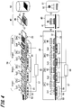
- FIG. 2 is a process flow chart showing an example of a manufacturing process applicable to the method for manufacturing an organic EL element of the present invention, and the organic EL element according to the present invention can be manufactured according to the flow shown in FIG.
- Stage 1 which is the first coating process, for example, in the organic EL element having the configuration shown in FIG. 1, the first organic functional layer L1 is formed on the substrate P formed up to the anode 2 using the first die coater Co1.
- the hole injection layer 3 shown in the configuration of FIG. 1 is formed by a wet coating method by a die coating method.
- the 1st organic functional layer L1 (for example, hole injection layer 3) formed on the board
- the substrate P is transferred to Stage 2 which is the second coating process.
- the second die coater Co2 is used, and for example, the hole transport layer 4 shown in the configuration of FIG. It is formed by a wet coating method using a die coating method.
- the 2nd organic functional layer L2 (for example, hole transport layer 4) formed on the board
- substrate P is transferred to the right side of a paper surface, and is dried in the drying part H2 as needed.
- the third organic functional layer L3 (for example, the light emitting layer 5) is prepared in Stage 3 as the third coating process, and the fourth organic functional layer L4 (for example, electron transport is performed in Stage 4 as the fourth coating process).
- the layer 6) is formed on the single wafer substrate P online.
- the single-wafer substrate P on which the organic functional layer group 20 is formed is transferred offline to the area 2 (40) having different atmospheric conditions, and finally dried by heat treatment (baking treatment) under specific atmospheric conditions. I do.
- the single-wafer substrate P on which the organic functional layer group 20 that has been subjected to the drying process is formed is transferred into a vapor deposition step 50, for example, a vacuum vapor deposition apparatus 51, and a desired constituent material is vapor deposited from a vapor deposition source 52. Then, the electron injection layer 7 and the cathode 8 are formed.
- a vapor deposition step 50 for example, a vacuum vapor deposition apparatus 51
- a desired constituent material is vapor deposited from a vapor deposition source 52.
- the cathode 8 After forming the cathode 8, it is sealed with a flexible sealing member 10 via a sealing adhesive 9 in a sealing step, and an organic EL element is manufactured.
- the second film forming environment 40 (area 2) is not performed without drying in the drying sections H1 to H4 in the first film forming environment 30 (area 1, Stages 1 to 4). ) May be collectively dried.
- FIG. 4 is a process flow diagram showing an example of a manufacturing process provided with a substrate floating unit as another example of the manufacturing method applicable to the method of manufacturing the organic EL element of the present invention. According to the flow shown in FIG. The organic EL device according to the invention can be manufactured. In FIG. 4, the same reference numerals are given to components common to FIG. 2.
- Stage 1 which is the first coating process, for example, in the organic EL element having the configuration shown in FIG. 1, the first organic functional layer L1 is formed on the substrate P formed up to the anode 2 using the first die coater Co1.
- the hole injection layer 3 shown in the configuration of FIG. 1 is formed by a wet coating method by a die coating method.
- the first organic functional layer L1 (for example, the hole injection layer 3) formed on the substrate P is transferred to the downstream side, and the organic solvent or the like is removed in the drying unit H1 of the drying zone D1 as necessary. Done.
- the substrate P is transferred to Stage 2 which is the second coating process.
- the second die coater Co2 is used, and for example, the hole transport layer 4 shown in the configuration of FIG. It is formed by a wet coating method using a die coating method.
- the second organic functional layer L2 (for example, the hole transport layer 4) formed on the substrate P is further transferred to the downstream side, and is dried in the drying unit H2 of the drying zone D2 as necessary.
- the third organic functional layer L3 (for example, the light emitting layer 5) is prepared in Stage 3 as the third coating process, and the fourth organic functional layer L4 (for example, electron transport is performed in Stage 4 as the fourth coating process).
- the layer 6) is formed on the single wafer substrate P online.
- the single-wafer substrate P on which the organic functional layer group 20 is formed is transferred offline to the area 2 (40) having different atmospheric conditions, and finally dried by heat treatment (baking treatment) under specific atmospheric conditions. I do.
- the single-wafer substrate P on which the organic functional layer group 20 that has been subjected to the drying process is formed is transferred into a vapor deposition step 50, for example, a vacuum vapor deposition apparatus 51, and a desired constituent material is vapor deposited from a vapor deposition source 52. Then, the electron injection layer 7 and the cathode 8 are formed.
- a vapor deposition step 50 for example, a vacuum vapor deposition apparatus 51
- a desired constituent material is vapor deposited from a vapor deposition source 52.
- the cathode 8 After forming the cathode 8, it is sealed with a flexible sealing member 10 via a sealing adhesive 9 in a sealing step, and an organic EL element is manufactured.
- the substrate holding member 32 having a porous structure being transported and having a gas permeability is provided on the back surface portion.
- a compressed gas for floating the substrate is supplied from a porous substrate floating unit 56 (described in detail later) installed in the substrate floating portion 55.
- the slant structure for example, the substrate holding member 32 shown in FIG. It is preferable that the hole is inclined to the right side.
- the distance between the bottom surface of the fixed die coater and the surface of the substrate P is affected by the displacement caused by vibration or the like during the transport of the substrate holding member 32.
- liquid breakage may occur due to an excessively wide bead gap, which causes an uncoated portion.
- the bead gap becomes excessively narrow, which causes a coating stripe.
- contact between the substrate holding member 32 and the substrate P during transportation may damage the edge portion of the substrate P, and may cause coating failure due to adhesion of generated dust or the like.
- the substrate P is applied to the substrate holding member 32 in a floating state, whereby the distance between the bottom surface of the die coater and the surface of the substrate P (bead).
- the gap also referred to as a gap
- FIG. 5 is a process flow diagram showing an example of a substrate floating unit that can be applied to the method of manufacturing an organic EL element of the present invention and has an endless transport belt 59 as a substrate holding member.
- FIG. Only 1 (30) is shown.
- the endless conveyance belt 59 held by the support roll 54 and the conveyance roll 53A as the substrate holding member is conveyed and installed in the substrate floating portion 55 in the same manner as the method shown in FIG.
- the porous substrate levitation unit 56 blows and sucks compressed gas for levitation of the substrate to the substrate, thereby applying the substrate while floating the substrate.
- the second film forming environment 40 (area 2) is not performed without drying in the drying sections H1 to H4 in the first film forming environment 30 (area 1, Stages 1 to 4). ) May be collectively dried.
- FIGS. 2 and 4 Coating environment for organic functional layer group
- a hole injection layer 3, a hole transport layer 4, and a light emitting layer 5 are formed on a single substrate P on which an anode is formed.
- the environmental (atmosphere) conditions in the step of forming the organic functional layer group 20 such as the electron transport layer 6 and the electron injection layer 7 and the subsequent drying step are mainly as follows: (I) Using each organic functional layer coating liquid constituting the organic functional layer group, in the first atmosphere 30 (area 1) in which the volume concentration of a gas other than the inert gas is 500 ppm or more, FIG. 2 and FIG.
- the compressed gas for flying the substrate in the step shown in FIG. 4 is also preferably a gas having a volume concentration of a gas other than the inert gas of 500 ppm or more.
- step (i) as a method for forming each organic functional layer, a die coating method that is a wet process is used.
- Examples of the solvent used to dissolve or disperse the organic EL material when preparing each organic functional layer coating solution according to the present invention include ketones such as methyl ethyl ketone and cyclohexanone, fatty acid esters such as ethyl acetate, diesters, and the like.
- Halogenated hydrocarbons such as chlorobenzene, aromatic hydrocarbons such as toluene, xylene, mesitylene, cyclohexylbenzene, aliphatic hydrocarbons such as cyclohexane, decalin, dodecane, dimethylformamide (DMF), dimethyl sulfoxide (DMSO), etc.
- These organic solvents can be used.
- as a dispersion method it can disperse
- the liquid preparation step for dissolving or dispersing the organic EL material is preferably performed under an inert gas atmosphere, and the organic functional layer is applied until it is applied onto the substrate by the flow shown in FIGS. It is preferable that the coating solution is a step that is not exposed to the coating atmosphere.
- the atmosphere (first film forming environment 30 (area 1)) and the compressed gas for floating the substrate when forming each organic functional layer are other than the inert gas.
- the volume concentration of the gas is preferably 500 ppm or more, which is considered optimal for forming a coating film of each organic functional layer.
- Examples of the gas other than the inert gas in the present invention include O 2 , O 3 , H 2 O, NOx, SOx and the like, preferably O 2 and H 2 O, and most preferable from the viewpoint of production cost. Is the atmosphere.
- the inert gas in the present invention is preferably a rare gas such as nitrogen gas, argon gas, or xenon gas, and most preferably nitrogen gas in terms of production cost.
- the inert gas in the coating atmosphere In the present invention, the effect of other gases does not remain on the outermost surface of the coating film, and gas molecules other than the inert gas enter the layer, resulting in a decrease in the performance of the organic EL element. As shown in 2, it is characterized in that it is continuously laminated without leaving a large coating interval.
- the coated and laminated organic functional layer group is collectively dried.
- Drying refers to a step of finally reducing the residual solvent ratio to 0.2% or less when the total solvent content of the laminated film immediately after coating is 100%.
- the means for drying generally used ones can be used, and examples thereof include reduced pressure or pressure drying, heat drying, air drying, IR drying, and electromagnetic wave drying.
- heat drying is preferable, and the temperature is equal to or higher than the boiling point of the solvent having the lowest boiling point among the solvents constituting the organic functional layer coating solution, and the material having the lowest Tg among the Tg of the organic functional layer material (Tg + 20) Most preferably, the temperature is maintained at a temperature lower than ° C. In the present invention, more specifically, it is preferable to hold and dry at 80 ° C. or higher and 150 ° C. or lower, and more preferable to hold and dry at 100 ° C. or higher and 130 ° C. or lower.
- the drying time is preferably 5 minutes or more and 300 minutes or less.
- the atmosphere at the time of drying the coating liquid after coating / lamination is an atmosphere in which the volume concentration of a gas other than the inert gas is 200 ppm or less.
- the second film-forming environment 40 (area 2) is also dried in an environment where the volume concentration of a gas other than the inert gas is 200 ppm or less even in the step (ii). It is preferable to have the process to make.
- gases other than the inert gas applicable in the step (ii) include O 2 , O 3 , H 2 O, NOx, and SOx.
- inert gas nitrogen gas and rare gases such as argon gas and xenon gas are preferable, and nitrogen gas is most preferable in terms of manufacturing cost.
- examples of wet coating methods include spin coating, casting, die coating, blade coating, roll coating, ink jet, printing, spray coating, and curtain coating.
- the invention is characterized in that a die coating method is used from the viewpoint of forming a highly accurate and uniform thin film.
- FIGS. 3 and 6 are a schematic sectional view of a slit type die coater applicable by the die coating method according to the present invention and a schematic view of a state in which coating is performed using the slit type die coater. That is, FIG. 3 and FIG. 6A is a schematic cross-sectional view of a state where coating is performed using a slit type die coater which is a pre-measuring type coating method. FIGS. 3 and 6B are schematic perspective views of the slit type die coater shown in FIGS.
- C indicates a slit type die coater.
- the slit type die coater C has two blocks 101a, a block 101b, a side plate 101c, and a side plate 101d, and is assembled by fastening with bolts or the like.
- Reference numeral 102 a denotes a notch provided at the end of the application width at the tip of the lip 103.
- Reference numeral 102 b denotes a notch provided at the end of the application width at the tip of the lip 103.
- the lip 103 has a back lip 103a and a front lip 103b.
- 104 indicates a slit formed by a gap between the block 101a and the block 101b, and 105 is a part for temporarily storing a coating liquid called a manifold, and the coating liquid is fed into the coating liquid supply pipe 106 here.
- the coating liquid stored in the coating width direction by the manifold 105 passes through the slit 104 and is supplied between the lip 103 and the single-wafer substrate P from the slit outlet 104a at the tip of the slit 104, and is applied.
- the supplied coating solution forms a bead and is coated on a single substrate P to form a coating film 107.
- the pressure at the slit outlet of the bead portion of the coating liquid supplied from the slit outlet 104a is applied on the single substrate P in a negative or zero state.
- the coating method using the slit type die coater C is a method that is performed without providing a decompression chamber.
- the application using the slit type die coater C as shown in FIGS. 3 and 6 is performed in accordance with the start of the application, with the required application liquid being supplied from the slit outlet, and moving means (not used) from the standby position to the application position. )
- This is a coating method in which a bead is formed in the coater gap between the lip and the substrate P, and the coating liquid is transferred to the substrate P (with liquid).
- the substrate P is supplied with the compressed gas A supplied from the substrate floating unit via the substrate holding member 32 and the vacuum pump as shown in FIG.
- suction B (not shown) and floating the substrate at a certain height H2 from the substrate holding member 32
- the height H2 (also referred to as a bead gap) between the lip 103 at the tip of the coating coater C and the substrate surface. ) Is controlled to a desired condition, and a stable bead is formed and applied.
- the gap H2 between the substrate holding member 32 and the substrate bottom is preferably in the range of 100 to 300 ⁇ m.
- the height H2 (bead gap) between the lip 103 at the tip of the coating coater C and the substrate surface, which is fixed, is preferably 100 to 700 ⁇ m, more preferably 200 to 500 ⁇ m. If the bead gap is 100 ⁇ m or more, the occurrence of coating stripes can be suppressed, and if it is 700 ⁇ m or less, the occurrence of liquid breakage or the like can be prevented.
- an organic functional layer is applied on a substrate as shown in FIGS. 2 to 3 and 4 to 6 using a die coater.
- the pattern of the layer may be a method of uniformly applying to almost the entire surface of the substrate, or a method of forming an organic functional layer by applying a specific pattern, for example, a stripe pattern or a lattice pattern in a specific pattern. good.
- the organic EL device manufacturing method of the present invention is characterized in that an organic functional layer is applied onto a substrate using a die coater in a state where the substrate is floated from a substrate holding member using a substrate floating unit.
- FIG. 7 is a schematic view showing an example of the configuration of a substrate floating unit applicable to the method for manufacturing an organic EL element of the present invention.
- the substrate floating unit shown in FIG. 7 is a schematic diagram showing in more detail the configuration of the substrate floating unit 55 shown in FIG. 4 and the substrate floating unit 56 installed therein.
- the substrate P is disposed on the substrate holding member 32, and the substrate floating portion 55 is disposed on the back surface of the substrate holding member 32.
- the substrate floating portion 55 is provided with two front and rear compressed gas supply units 300A and 300B each including a chamber 302 for supplying a compressed gas A1 for floating the substrate P and a substrate floating unit 301.
- the substrate floating unit 301 is made of a porous material having a gas passage that penetrates in the film thickness direction as described above.
- a decompression unit 306 for intake A3 is provided between the two compressed gas supply units 300A and 300B.
- the floating amount H1 of the substrate P relative to the substrate holding member 32 is detected by the position detection sensor 307 provided in the vicinity of the substrate holding member 32.
- the compressed gas flow rate is adjusted so that the height H2 (bead gap) between the tip lip of the coating coater Co and the surface of the substrate P becomes a desired condition.
- the supply amount A1 is controlled through the information line 308 to the operation amount of the gas blowing pumps 304A and 304B.
- the operating amount of the vacuum pump 305 via the information line 309 and balancing the conditions of the intake air A3, a desired substrate flying height H2 is realized.
- a method of transporting the levitated substrate in the right direction of the paper for example, a method of transporting the substrate by pushing the rear end portion of the substrate with an air cylinder or the like, or in two installed compressed gas supply units 300
- the substrate floating unit having such a configuration can be obtained as a commercial product.
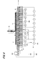
- FIG. 8 shows an example of another configuration of the substrate floating unit applicable to the method for manufacturing the organic EL element of the present invention.
- the substrate floating unit 310 shown in FIG. 8 is installed over the entire surface of the substrate holding member 32, and two pairs of compressed gas blowing units 311 for floating the substrate P and a suction unit for reducing the pressure by the vacuum pump 305. 312 are alternately arranged on the entire surface to constitute a substrate floating unit 310.
- An independent pump 304 is connected to each of the two pairs of compressed gas blowing sections 311, and the supply amount A of the compressed gas is determined based on the floating amount H1 information of the substrate P with respect to the substrate holding member 32 by the position detection sensor 307.
- the operation amount of P1 to P9 of the gas blower pump 304 is controlled via the information line 308.
- the intake air amount B of the vacuum pump 305 is controlled based on the floating amount H1 information of the substrate P with respect to the substrate holding member 32 by the position detection sensor 307.
- the pumps 0P1 to P9 are operated so that the compressed gas supply amount A gradually decreases from the upstream pump P1 to the downstream pump P9. It is preferred to control the amount.
- an alignment mark is provided on a single wafer substrate, the alignment mark is detected, and an organic functional layer forming coating is applied from the die coater to the single wafer substrate. It is preferable to control the supply and stop of the liquid.
- the substrate floating unit is operated in accordance with the application start time information to float the substrate.
- an alignment mark As shown in FIG. 9, it can be applied to each corner portion of the substrate as a corner registration mark.
- ITO indium tin oxide
- the mark can be formed by forming a film by a sputtering method.
- a CCD camera 401 is installed on the upstream side of Stage 1 which is the first coating zone so as to cover the entire width of the substrate, Based on the detection and position information and the substrate conveyance speed information, the application start time (supply start time of the organic functional layer forming coating liquid to the die coater) and the application completion time (organic function) on the substrate P are determined.
- the application of the coating liquid for layer formation to the die coater is instructed to each coater (Co1 to Co3 shown in FIG. 9) via the feedback circuit 404 to control the application.
- the substrate floating unit is operated at a predetermined time to lift the substrate. Apply.
- the supply of the organic functional layer forming coating liquid to the die coater is stopped in the uncoated stage due to the detection of the alignment mark by the CCD camera and the position information.
- the coating liquid for forming the organic functional layer which has been stopped, forms a meniscus and is directly exposed to the outside air.
- the coating film is formed by evaporating the solvent from the surface of the coating liquid for forming the organic functional layer in contact with the outside air, and the droplets of the coating liquid for forming the organic functional layer scattered during the coating process are formed on the die coater. It solidifies at the lip and causes a coating failure.
- the wiping cleaning process is performed on the lip surface of the die coater when the coating solution to the die coater is stopped.
- the die coater Co 2 and Co 3 are respectively supplied at the time when supply of the organic functional layer forming coating liquid to the die coater is stopped.
- the lip surface of the die coater is cleaned using a cleaning liquid by moving the wiping cleaning processing apparatus 403 from the coating position to the position of the wiping cleaning processing apparatus 403.
- information is again transmitted to the die coater via the feedback circuit 404. After the die coater is moved to each coating position, the organic functional layer forming coating solution is supplied at the coating start time. Start application.
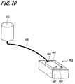
- FIG. 10 shows an example of a main configuration of a die coater wiping cleaning apparatus applicable to the present invention.
- the wiping cleaning device 403 includes a wiping member 409 that protrudes upward and a sheet-like flexible member 408 that supports the wiping member 409 in a box-shaped housing 407. Then, after the wipe unit 406 itself is moved upward by a drive source such as a motor (not shown), the die coater is moved to the upper part of the wiping member 409, and the nozzle surface of the wiping member 409 and the head Co (103 shown in FIG. 6). ) Are in contact with each other, the wiping member 409 rubs the nozzle surface 103 of the head Co to remove the sticking matter adhering to the entire nozzle surface 103, the dry film on the meniscus portion, and the like. When the wiping operation is completed, the wiping unit 406 is lowered, and the contact state between the wiping member 409 and the nozzle surface 103 is released.
- a drive source such as a motor
- a cleaning liquid tank 410 is connected to the wipe unit 406 via a liquid supply path 405.
- a cleaning liquid supply valve (not shown) is provided in the middle of the liquid supply path 405.
- the liquid supply path 405 is a path through which the cleaning liquid flows by the operation of the cleaning liquid supply valve, and is constituted by, for example, a resin tube.
- the cleaning liquid tank 410 is disposed at a position higher than the position of the wipe unit 406 (the position of the wiping member 409), the cleaning liquid can be easily supplied to the wiping member 409 due to a water head difference.
- the cleaning liquid As the cleaning liquid, it is required to have a function of reliably wiping the organic functional layer forming coating liquid adhering to the nozzle surface by dissolving, redispersing, and softening. Therefore, the cleaning liquid preferably contains a solution component constituting the coating liquid for forming an organic functional layer, for example, various solvents, water, a surfactant, a basic compound, and the like, but is not limited thereto. Is not to be done. In particular, when a solvent having a low surface tension is contained, it is effective because it easily penetrates into the dried coating material for forming a functional layer. Moreover, it is preferable to contain a basic compound in order to accelerate
- injection layer hole injection layer, electron injection layer
- the injection layer can be provided as necessary.
- the injection layer includes an electron injection layer and a hole injection layer, and may be present between the anode and the light emitting layer or the hole transport layer and between the cathode and the light emitting layer or the electron transport layer as described above.
- the injection layer referred to in the present invention is a layer provided between the electrode and the organic functional layer in order to lower the driving voltage and improve the light emission luminance.
- Injection materials include triazole derivatives, oxadiazole derivatives, imidazole derivatives, pyrazoline derivatives and pyrazolone derivatives, phenylenediamine derivatives, arylamine derivatives, amino-substituted chalcone derivatives, oxazole derivatives, styrylanthracene derivatives, fluorenone derivatives, hydrazone derivatives, stilbene derivatives.
- the details of the electron injection layer are described in, for example, JP-A-6-325871, JP-A-9-17574, and JP-A-10-74586, and specific examples thereof include strontium and aluminum.
- the buffer layer (injection layer) is desirably a very thin film, and potassium fluoride and sodium fluoride are preferable.
- the film thickness is about 0.1 nm to 5 ⁇ m, preferably 0.1 to 100 nm, more preferably 0.5 to 10 nm, and most preferably 0.5 to 4 nm.
- the electron injection layer is preferably formed by a vapor deposition method using a vacuum vapor deposition apparatus or the like instead of a wet coating method.
- hole transport layer As the hole transport material constituting the hole transport layer, the same compounds as those applied in the hole injection layer can be used, but further, porphyrin compounds, aromatics It is preferable to use a tertiary amine compound and a styrylamine compound, particularly an aromatic tertiary amine compound.
- aromatic tertiary amine compounds and styrylamine compounds include N, N, N ′, N′-tetraphenyl-4,4′-diaminophenyl; N, N′-diphenyl-N, N′— Bis (3-methylphenyl)-[1,1′-biphenyl] -4,4′-diamine (TPD); 2,2-bis (4-di-p-tolylaminophenyl) propane; 1,1-bis (4-di-p-tolylaminophenyl) cyclohexane; N, N, N ′, N′-tetra-p-tolyl-4,4′-diaminobiphenyl; 1,1-bis (4-di-p-tolyl) Aminophenyl) -4-phenylcyclohexane; bis (4-dimethylamino-2-methylphenyl) phenylmethane; bis (4-di-p-tolylaminoph
- polymer materials in which these materials are introduced into polymer chains or these materials are used as polymer main chains can also be used.
- inorganic compounds such as p-type-Si and p-type-SiC can also be used as the hole injection material and the hole transport material.
- JP-A-4-297076 JP-A-2000-196140, JP-A-2001-102175, J. Pat. Appl. Phys. , 95, 5773 (2004), JP-A-11-251067, J. MoI. Huang et. al. It is also possible to use a hole transport material that has so-called p-type semiconducting properties, as described in the literature (Applied Physics Letters 80 (2002), p. 139), JP 2003-519432 A. it can.
- the hole transport layer is formed by thinning a coating solution containing the hole transport material by a die coating method.
- the thickness of the hole transport layer is not particularly limited, but is usually about 5 nm to 5 ⁇ m, preferably 5 to 200 nm.
- the hole transport layer may have a single layer structure composed of one or more of the above materials.
- Electron transport layer is made of a material having a function of transporting electrons, and in a broad sense, an electron injection layer and a hole blocking layer are also included in the electron transport layer.
- the electron transport layer can be provided as a single layer or a plurality of layers.
- an electron transport material also serving as a hole blocking material used for an electron transport layer adjacent to the cathode side with respect to the light emitting layer is injected from the cathode.
- any material can be selected and used from among conventionally known compounds.
- fluorene derivatives, carbazole derivatives, azacarbazole And metal complexes such as derivatives, oxadiazole derivatives, triazole derivatives, silole derivatives, pyridine derivatives, pyrimidine derivatives, 8-quinolinol derivatives, and the like.
- metal-free or metal phthalocyanine or those having terminal ends substituted with an alkyl group or a sulfonic acid group can be preferably used as the electron transporting material.
- carbazole derivatives azacarbazole derivatives, pyridine derivatives and the like are preferable in the present invention, and more preferably an azacarbazole derivative.
- the electron transport layer is formed by a wet process using a die coating method with an electron transport layer coating solution containing the electron transport material, semiconductor nanoparticles (see below), and a fluorinated alcohol solvent.
- the thickness of the electron transport layer is not particularly limited, but is usually about 5 nm to 5 ⁇ m, preferably 5 to 200 nm.
- the electron transport layer may have a single layer structure composed of one or more of the above materials.
- an electron transport layer having a high n property doped with an impurity as a guest material can also be used.
- examples thereof include JP-A-4-297076, JP-A-10-270172, JP-A-2000-196140, 2001-102175, J.A. Appl. Phys. 95, 5773 (2004), and the like.
- the electron transport layer in the present invention preferably contains an organic alkali metal salt.
- organic alkali metal salt there are no particular restrictions on the type of organic substance, but formate, acetate, propionic acid, butyrate, valerate, caproate, enanthate, caprylate, oxalate, malonate, succinate Benzoate, phthalate, isophthalate, terephthalate, salicylate, pyruvate, lactate, malate, adipate, mesylate, tosylate, benzenesulfonate , Preferably formate, acetate, propionate, butyrate, valerate, caprate, enanthate, caprylate, oxalate, malonate, succinate, benzoate, more preferably Is preferably an alkali metal salt of an aliphatic carboxylic acid such as formate, acetate, propionate or butyrate, and the aliphatic carboxylic acid preferably has 4
- the type of alkali metal of the organic alkali metal salt is not particularly limited, and examples thereof include Na, K, and Cs, preferably K, Cs, and more preferably Cs.
- the alkali metal salt of the organic substance include a combination of the organic substance and the alkali metal, preferably, formic acid Li, formic acid K, Na formic acid, formic acid Cs, Li acetate, K acetate, Na acetate, Cs acetate, Lipropionate, Propionic acid Na, propionic acid K, propionic acid Cs, oxalic acid Li, oxalic acid Na, oxalic acid K, oxalic acid Cs, malonic acid Li, malonic acid Na, malonic acid K, malonic acid Cs, succinic acid Li, succinic acid Na, succinic acid K, succinic acid Cs, benzoic acid Li, benzoic acid Na, benzoic acid K, benzoic acid Cs, more preferably Li acetate,
- the content of these dope materials is preferably 1.5 to 35% by mass, more preferably 3 to 25% by mass, and most preferably 5 to 15% by mass with respect to the electron transport layer to be added.
- the light emitting layer constituting the organic EL device according to the present invention is a layer that emits light by recombination of electrons and holes injected from the electrode, the electron transport layer, or the hole transport layer, and emits light.
- the portion to be formed may be in the light emitting layer or at the interface between the light emitting layer and the adjacent layer.
- the structure of the light emitting layer according to the present invention is not particularly limited as long as the light emitting material included satisfies the above requirements.
- the total thickness of the light emitting layers is preferably in the range of 1 to 100 nm, and more preferably 50 nm or less because a lower driving voltage can be obtained.
- the sum total of the film thickness of the light emitting layer as used in this invention is a film thickness also including the said intermediate
- each light emitting layer it is preferable to adjust the film thickness of each light emitting layer to a range of 1 to 50 nm.
- the film thicknesses of the blue, green and red light emitting layers There is no particular limitation on the relationship between the film thicknesses of the blue, green and red light emitting layers.
- the light emitting layer is formed by forming a light emitting layer forming coating solution containing a light emitting material and a host compound described later by a die coating method.
- a plurality of light emitting materials may be mixed in each light emitting layer, or a phosphorescent light emitting material and a fluorescent light emitting material may be mixed and used in the same light emitting layer.
- the light emitting layer preferably contains a host compound and a light emitting material (also referred to as a light emitting dopant compound) and emits light from the light emitting material.
- a light emitting material also referred to as a light emitting dopant compound
- ⁇ 4.1 Host compound>
- a compound having a phosphorescence quantum yield of phosphorescence emission at room temperature (25 ° C.) of less than 0.1 is preferable. More preferably, the phosphorescence quantum yield is less than 0.01. Moreover, it is preferable that the volume ratio in the layer is 50% or more among the compounds contained in a light emitting layer.
- known host compounds may be used alone or in combination of two or more.
- the organic EL element can be made highly efficient.
- the light emitting host used in the present invention may be a conventionally known low molecular compound or a high molecular compound having a repeating unit, and a low molecular compound having a polymerizable group such as a vinyl group or an epoxy group (polymerizable light emission).
- a high molecular weight material when used, a phenomenon in which the compound is likely to be difficult to escape, such as swelling or gelation, due to the compound taking in the solvent is likely to occur.
- the known host compound a compound that has a hole transporting ability and an electron transporting ability, prevents the emission of light from being increased in wavelength, and has a high Tg (glass transition temperature) is preferable.
- the glass transition point (Tg) is a value determined by a method based on JIS-K-7121 using DSC (Differential Scanning Colorimetry).
- the host compound used in the present invention is preferably a carbazole derivative, more preferably a carbazole derivative and a dibenzofuran compound.
- Luminescent dopant As the light emitting dopant according to the present invention, a fluorescent dopant or a phosphorescent dopant can be used. From the viewpoint of obtaining an organic EL element with higher luminous efficiency, the light emitting layer or light emitting unit of the organic EL element according to the present invention is used. As a light emitting dopant to be used, it is preferable to contain a phosphorescent dopant simultaneously with the above-mentioned light emitting host.
- the phosphorescent dopant according to the present invention is a compound in which light emission from an excited triplet is observed.
- the phosphorescent dopant is a compound that emits phosphorescence at room temperature (25 ° C.) and has a phosphorescence quantum yield of 25. Although it is defined as a compound of 0.01 or more at ° C., a preferable phosphorescence quantum yield is 0.1 or more.
- the phosphorescent quantum yield can be measured by the method described in Spectroscopic II, page 398 (1992 edition, Maruzen) of the Fourth Edition Experimental Chemistry Course 7. Although the phosphorescence quantum yield in a solution can be measured using various solvents, the phosphorescence dopant according to the present invention achieves the phosphorescence quantum yield (0.01 or more) in any solvent. That's fine.
- phosphorescent dopants There are two types of emission of phosphorescent dopants in principle. One is the recombination of carriers on the light-emitting host on which carriers are transported to generate the excited state of the light-emitting host, and this energy is transferred to the phosphorescent dopant. Energy transfer type to obtain light emission from the phosphorescent dopant, another is that the phosphorescent dopant becomes a carrier trap, carrier recombination occurs on the phosphorescent dopant, and light emission from the phosphorescent dopant is obtained Although it is a carrier trap type, in any case, it is a condition that the excited state energy of the phosphorescent dopant is lower than the excited state energy of the light emitting host.
- the phosphorescent dopant can be appropriately selected from known materials used for the light emitting layer of the organic EL element.
- the phosphorescent dopant applicable to the present invention is preferably a complex compound containing a metal belonging to Group 8, Group 9, or Group 10 of the periodic table of elements, and more preferably an iridium compound, a platinum compound, or an osmium compound. , Palladium compounds and rhodium compounds, and most preferred are iridium compounds and platinum compounds.
- the light emitting dopant contained in the light emitting layer may be one kind, or may contain two or more kinds of light emitting dopants having different light emission maximum wavelengths.
- a concentration gradient may be formed in the thickness direction of the light emitting layer for all the light emitting dopants, but only one kind of light emitting dopant may be formed.
- the concentration gradient is formed only for one kind of light emitting dopant, it is preferable to form the concentration gradient for the light emitting dopant having the shortest wavelength of the light emission maximum wavelength.
- an electrode material made of a metal, an alloy, an electrically conductive compound or a mixture thereof having a high work function (4 eV or more) is preferably used.
- electrode materials include metals such as Au, and conductive transparent materials such as CuI, indium tin oxide (ITO), SnO 2 , and ZnO.
- conductive transparent materials such as CuI, indium tin oxide (ITO), SnO 2 , and ZnO.
- an amorphous material such as IDIXO (In 2 O 3 —ZnO) capable of forming a transparent conductive film may be used.
- these electrode materials may be formed into a thin film by a method such as vapor deposition or sputtering, and a desired shape pattern may be formed by a photolithography method, or when pattern accuracy is not so high (about 100 ⁇ m or more)
- a pattern may be formed through a mask having a desired shape at the time of vapor deposition or sputtering of the electrode material.
- wet film-forming methods such as a printing system and a coating system, can also be used.
- the transmittance is greater than 10%, and the sheet resistance as the anode is preferably several hundred ⁇ / ⁇ or less.
- the film thickness depends on the material, it is usually in the range of 10 to 1000 nm, preferably in the range of 10 to 200 nm.
- cathode a material having a low work function (4 eV or less) metal (referred to as an electron injecting metal), an alloy, an electrically conductive compound, and a mixture thereof as an electrode material is used.
- electrode materials include sodium, sodium-potassium alloy, magnesium, lithium, magnesium / copper mixture, magnesium / silver mixture, magnesium / aluminum mixture, magnesium / indium mixture, aluminum / aluminum oxide (Al 2 O 3 ) Mixtures, indium, lithium / aluminum mixtures, rare earth metals and the like.
- a mixture of an electron injecting metal and a second metal which is a stable metal having a larger work function than this for example, a magnesium / silver mixture, Magnesium / aluminum mixtures, magnesium / indium mixtures, aluminum / aluminum oxide (Al 2 O 3 ) mixtures, lithium / aluminum mixtures, aluminum and the like are preferred.
- the cathode can be produced by forming a thin film of these electrode materials by a method such as vapor deposition or sputtering.
- the sheet resistance as the cathode is preferably several hundred ⁇ / ⁇ or less, and the film thickness is usually selected in the range of 10 nm to 5 ⁇ m, preferably 50 to 200 nm.
- the light emission luminance is improved, which is convenient.
- a transparent or translucent cathode can be produced by forming the above metal on the cathode with a film thickness of 1 to 20 nm and then forming the conductive transparent material mentioned in the description of the anode thereon.
- an organic EL element in which both the anode and the cathode are transmissive can be produced.
- substrate There are no particular limitations on the type of glass, plastic, etc., which can be used in the organic EL device according to the present invention (hereinafter also referred to as a support base, support substrate, substrate, support, etc.), and it is transparent. Or opaque. When extracting light from the support substrate side, the support substrate is preferably transparent. Examples of the transparent support substrate preferably used include glass, quartz, and a transparent resin film, and a glass substrate is particularly preferable.
- glass substrate examples include soda lime glass, barium / strontium-containing glass, lead glass, aluminosilicate glass, borosilicate glass, barium borosilicate glass, and quartz.
- polyesters such as polyethylene terephthalate (PET) and polyethylene naphthalate (PEN), polyethylene, polypropylene, cellophane, cellulose diacetate, cellulose triacetate, cellulose acetate butyrate, cellulose acetate propionate (CAP), Cellulose esters such as cellulose acetate phthalate (TAC) and cellulose nitrate or derivatives thereof, polyvinylidene chloride, polyvinyl alcohol, polyethylene vinyl alcohol, syndiotactic polystyrene, polycarbonate, norbornene resin, polymethylpentene, polyether ketone, polyimide , Polyethersulfone (PES), polyphenylene sulfide, polysulfone , Polyetherimide, polyetherketoneimide, polyamide, fluororesin, nylon, polymethylmethacrylate, acrylic or polyarylates, cyclone resins such as Arton (trade name, manufactured by JSR) or Appel (trade
- an inorganic film, an organic film or a hybrid film of both may be formed on the surface of the resin film.
- a relative humidity (90 ⁇ 2)% RH) of 0.01 g / (m 2 ⁇ 24 h) or less is preferable, and oxygen permeability measured by a method according to JIS K 7126-1987.
- the film is preferably a high barrier film having a degree of 1 ⁇ 10 ⁇ 3 cm 3 / (m 2 ⁇ 24 h ⁇ atm) or less and a water vapor permeability of 1 ⁇ 10 ⁇ 3 g / (m 2 ⁇ 24 h) or less, More preferably, the water vapor permeability is 1 ⁇ 10 ⁇ 5 g / (m 2 ⁇ 24 h) or less.
- any material may be used as long as it has a function of suppressing entry of factors that cause deterioration of the organic EL element such as moisture and oxygen.
- silicon oxide, silicon dioxide, silicon nitride, or the like is used. Can do.
- laminate stack both alternately several times.
- the method for forming the barrier film is not particularly limited.
- the vacuum deposition method, sputtering method, reactive sputtering method, molecular beam epitaxy method, cluster ion beam method, ion plating method, plasma polymerization method, atmospheric pressure plasma A polymerization method, a plasma CVD method, a laser CVD method, a thermal CVD method, a coating method, and the like can be used, but an atmospheric pressure plasma polymerization method as described in JP-A-2004-68143 is particularly preferable.
- the opaque support substrate examples include metal plates such as aluminum and stainless steel, films, opaque resin substrates, ceramic substrates, and the like.
- the external extraction efficiency of light emission at room temperature is preferably 1% or more, more preferably 5% or more.
- the external extraction quantum efficiency (%) the number of photons emitted to the outside of the organic EL element / the number of electrons sent to the organic EL element ⁇ 100.
- Sealing adhesive, sealing member As a sealing means applicable to the organic EL element according to the present invention, for example, a method of adhering a sealing member, an electrode, and a support substrate with an adhesive can be mentioned.
- the sealing member may be disposed so as to cover the display area of the organic EL element, and may be a concave plate shape or a flat plate shape. Further, transparency and electrical insulation are not particularly limited.
- Specific examples include a glass plate, a polymer plate / film, and a metal plate / film.
- the glass plate include soda-lime glass, barium / strontium-containing glass, lead glass, aluminosilicate glass, borosilicate glass, barium borosilicate glass, and quartz.
- the polymer plate include polycarbonate, acrylic, polyethylene terephthalate, polyether sulfide, and polysulfone.
- the metal plate include those made of one or more metals or alloys selected from the group consisting of stainless steel, iron, copper, aluminum, magnesium, nickel, zinc, chromium, titanium, molybdenum, silicone, germanium, and tantalum.
- a polymer film and a metal film can be preferably used because the element can be thinned.
- the polymer film has an oxygen permeability measured by a method according to JIS K 7126-1987 of 1 ⁇ 10 ⁇ 3 ml / (m 2 ⁇ 24 h ⁇ atm) or less, and conforms to JIS K 7129-1992.
- the water vapor permeability (25 ⁇ 0.5 ° C., relative humidity (90 ⁇ 2)% RH) measured by the method is preferably 1 ⁇ 10 ⁇ 3 g / (m 2 ⁇ 24 h) or less.
- sealing member For processing the sealing member into a concave shape, sandblasting, chemical etching, or the like is used.
- the adhesive include photocuring and thermosetting adhesives having reactive vinyl groups of acrylic acid oligomers and methacrylic acid oligomers, and moisture curing adhesives such as 2-cyanoacrylates. Can be mentioned. Moreover, heat
- an organic EL element may deteriorate by heat processing, what can be adhesively cured from room temperature to 80 ° C. is preferable. Further, a desiccant may be dispersed in the adhesive. Application
- coating of the adhesive agent to a sealing part may use commercially available dispenser, and may print like screen printing.
- the electrode and the organic functional layer are coated on the outside of the electrode facing the support substrate with the organic functional layer interposed therebetween, and an inorganic or organic layer is formed in contact with the support substrate to form a sealing film.
- the material for forming the film may be any material that has a function of suppressing intrusion of elements that cause deterioration of elements such as moisture and oxygen.
- silicon oxide, silicon dioxide, silicon nitride, or the like may be used. it can.
- vacuum deposition sputtering, reactive sputtering, molecular beam epitaxy, cluster ion beam method, ion plating method, plasma polymerization method, atmospheric pressure plasma
- a polymerization method a plasma CVD method, a laser CVD method, a thermal CVD method, a coating method, or the like can be used.
- an inert gas such as nitrogen or argon, an inert gas such as fluorinated hydrocarbon or silicon oil is used. It is preferable to inject a liquid. A vacuum is also possible. Moreover, a hygroscopic compound can also be enclosed inside.
- hygroscopic compound examples include metal oxides (for example, sodium oxide, potassium oxide, calcium oxide, barium oxide, magnesium oxide, aluminum oxide) and sulfates (for example, sodium sulfate, calcium sulfate, magnesium sulfate, cobalt sulfate).
- metal oxides for example, sodium oxide, potassium oxide, calcium oxide, barium oxide, magnesium oxide, aluminum oxide
- sulfates for example, sodium sulfate, calcium sulfate, magnesium sulfate, cobalt sulfate.
- metal halides eg calcium chloride, magnesium chloride, cesium fluoride, tantalum fluoride, cerium bromide, magnesium bromide, barium iodide, magnesium iodide etc.
- perchloric acids eg perchloric acid Barium, magnesium perchlorate, and the like
- anhydrous salts are preferably used in sulfates, metal halides, and perchloric acids.
- Sealing includes casing type sealing (can sealing) and close contact type sealing (solid sealing), but solid sealing is preferable from the viewpoint of thinning. Moreover, when producing a flexible organic EL element, since sealing is also required for the sealing member, solid sealing is preferable.
- thermosetting adhesive an ultraviolet curable resin, or the like
- a thermosetting adhesive such as an epoxy resin, an acrylic resin, or a silicone resin, more preferably moisture resistant. It is an epoxy thermosetting adhesive resin that is excellent in water resistance and water resistance and has little shrinkage during curing.
- the water content of the sealing adhesive according to the present invention is preferably 300 ppm or less, more preferably 0.01 to 200 ppm, and most preferably 0.01 to 100 ppm.
- the moisture content referred to in the present invention may be measured by any method.
- a volumetric moisture meter Karl Fischer
- an infrared moisture meter a microwave transmission moisture meter
- a heat-dry weight method e.g., a heat-dry weight method
- GC / MS e.g., a volumetric moisture meter
- IR IR
- DSC differential scanning calorimeter
- TDS temperature programmed desorption analysis
- the moisture content of the sealing adhesive can be adjusted by, for example, placing it in a nitrogen atmosphere with a dew point temperature of ⁇ 80 ° C. or lower and an oxygen concentration of 0.8 ppm, and changing the time. Further, it can be dried in a vacuum state of 100 Pa or less while changing the time. Further, the sealing adhesive can be dried only with an adhesive, but can also be placed in advance on the sealing member and dried.
- the sealing member for example, a 50 ⁇ m thick PET (polyethylene terephthalate) laminated with an aluminum foil (30 ⁇ m thick) is used. Using this as a sealing member, it is uniformly applied to the aluminum surface using a dispenser, a sealing adhesive is placed in advance, the resin substrate 1 and the sealing member 5 are aligned, and both are pressure-bonded ( 0.1-3 MPa) and a temperature of 80-180 ° C. for close contact / bonding (adhesion), and close sealing (solid sealing).
- Heating or pressure bonding time varies depending on the type, amount, and area of the adhesive, but temporary bonding is performed at a pressure of 0.1 to 3 MPa, and heat curing time is in the range of 5 seconds to 10 minutes at a temperature of 80 to 180 ° C. Just choose.
- a heated pressure-bonding roll because pressure bonding (temporary bonding) and heating can be performed simultaneously, and internal voids can be eliminated simultaneously.
- a coating method such as roll coating, spin coating, screen printing, spray coating, or the like can be used using a dispenser depending on the material.
- solid sealing is a form in which there is no space between the sealing member and the organic EL element substrate and the resin is covered with a cured resin.
- the sealing member include metals such as stainless steel, aluminum, and magnesium alloys, polyethylene terephthalate, polycarbonate, polystyrene, nylon, plastics such as polyvinyl chloride, and composites thereof, glass, and the like.
- a laminate of gas barrier layers such as aluminum, aluminum oxide, silicon oxide, and silicon nitride can be used as in the case of a resin substrate.
- the gas barrier layer can be formed by sputtering, vapor deposition or the like on both surfaces or one surface of the sealing member before molding the sealing member, or may be formed on both surfaces or one surface of the sealing member after sealing by a similar method.
- the oxygen permeability is 1 ⁇ 10 ⁇ 3 ml / (m 2 ⁇ 24 h ⁇ atm) or less
- the water vapor permeability (25 ⁇ 0.5 ° C., relative humidity (90 ⁇ 2)% RH) is 1 ⁇ It is preferably 10 ⁇ 3 g / (m 2 ⁇ 24 h) or less.
- the sealing member may be a film laminated with a metal foil such as aluminum.
- a method for laminating the polymer film on one side of the metal foil a generally used laminating machine can be used.
- the adhesive polyurethane-based, polyester-based, epoxy-based, acrylic-based adhesives and the like can be used. You may use a hardening
- a hot melt lamination method, an extrusion lamination method and a coextrusion lamination method can also be used, but a dry lamination method is preferred.
- the metal foil when the metal foil is formed by sputtering or vapor deposition, and is formed from a fluid electrode material such as a conductive paste, the metal foil may be formed by using a polymer film as a substrate. .
- a protective film or a protective plate may be provided outside the sealing film on the side facing the support substrate with the organic functional layer interposed therebetween or on the outer side of the sealing film.
- the mechanical strength is not necessarily high, and thus it is preferable to provide such a protective film and a protective plate.
- the same glass plate, polymer plate / film, metal plate / film, and the like used for the sealing can be used.
- the polymer film is light and thin. Is preferably used.
- the light extraction member is provided between the substrate and the anode or at any location on the light emission side from the substrate.
- Examples of the light extraction member include a prism sheet, a lens sheet, and a diffusion sheet. Further, a diffraction grating or a diffusion structure introduced into an interface or any medium that causes total reflection can be used.
- an organic electroluminescence element that emits light from a substrate
- a part of the light emitted from the light emitting layer causes total reflection at the interface between the substrate and air, causing a problem of loss of light.
- prismatic or lens-like processing is applied to the surface of the substrate, or prism sheets, lens sheets, and diffusion sheets are affixed to the surface of the substrate, thereby suppressing total reflection and light extraction efficiency. To improve.
- the organic EL element according to the present invention can be used as a display device, a display, and various light sources.
- Examples of light sources include home lighting, interior lighting, clock and liquid crystal backlights, billboard advertisements, traffic lights, light sources for optical storage media, light sources for electrophotographic copying machines, light sources for optical communication processors, and light sources for optical sensors. Furthermore, it can be used in a wide range of applications such as general household appliances that require a display device, but it can be used effectively as a backlight for a liquid crystal display device combined with a color filter, and as a light source for illumination. it can.
- patterning may be performed by a metal mask, an inkjet printing method, or the like at the time of film formation, if necessary.
- patterning only the electrode may be patterned, the electrode and the light emitting layer may be patterned, or the entire layer of the organic EL element may be patterned. The method can be used.
- Example 1 Production of organic EL element >> [Preparation of Organic EL Element 101: Formation of Organic Functional Layer by Vacuum Deposition Method] (Formation of anode) After patterning on a glass substrate (NH techno glass, NA45) in which ITO (indium tin oxide) was formed into a film with a thickness of 150 nm on a glass substrate having a thickness of 150 mm ⁇ 150 mm and a thickness of 1.1 mm, The substrate provided with the ITO transparent electrode was subjected to ultrasonic cleaning with isopropyl alcohol, dried with dry nitrogen gas, and UV ozone cleaning was performed for 5 minutes.
- ITO indium tin oxide
- the glass substrate having the ITO transparent electrode was fixed to a substrate holder in a plasma processing chamber connected to a commercially available vacuum deposition apparatus.
- each of the vapor deposition crucibles in the vacuum vapor deposition apparatus was filled with an optimum amount of the constituent material of each layer for producing the organic EL element.
- the evaporation crucible used was made of a resistance heating material made of molybdenum or tungsten.
- the substrate After performing a plasma treatment for 2 minutes at an oxygen pressure of 1 Pa and an electric power of 100 W (electrode area: about 450 cm 2 ), the substrate is transferred to each vapor deposition chamber of the organic EL constituent layer without being exposed to the atmosphere. Film formation was performed.
- the deposition crucible containing m-MTDATA was energized and heated, and deposited on a transparent support substrate at a deposition rate of 0.1 nm / sec. A hole injection layer was provided. Next, ⁇ -NPD was deposited in the same manner to provide a 30 nm hole transport layer.
- each light emitting layer was formed according to the following procedure.
- Compound M-1 was deposited to a thickness of 50 nm to form a layer having hole blocking and electron transport functions, and LiF was deposited to a thickness of 1 nm to form an electron transport layer.
- FIG. 11 is a schematic diagram showing an example of a production line for forming an organic functional layer by a batch method as a comparative example.
- positioning pins 202 for determining the installation position of the substrate P on which the anode 203 is formed are provided on the holding member 201 at four locations. Then, the substrate P on which the anode 203 is formed is carried in.
- the substrate P placed on the holding member 201 is suction-fixed.
- a first organic functional layer L1 (for example, a hole injection layer) is formed on the anode 203 using a slit type die coater Co having the configuration shown in FIG.
- the drying unit H performs drying by blowing heated hot air 204 onto the formed first organic functional layer L ⁇ b> 1.
- the substrate P placed on the holding member 201 is removed and removed to form the first organic functional layer, and the processes a) to f) are sequentially performed. Repeatedly, an organic functional layer group was formed.
- This ITO transparent electrode was formed by patterning a substrate (NH technoglass NA45) in which ITO (indium tin oxide) was formed as a positive electrode 203 on a glass substrate P of 150 mm ⁇ 150 mm ⁇ 1.1 mm with a thickness of 150 nm.
- a substrate P also referred to as an ITO substrate
- poly (3,4-ethylenedioxythiophene) -polystyrene sulfonate (PEDOT / PSS, manufactured by Bayer, Baytron P Al 4083) is purified on the anode 203 of the mounted substrate P.
- the hole injection layer coating solution 1 diluted to 70% with water was set at a coating speed of 3 m / min, and the temperature during coating of the hole injection layer forming coating solution was set to 25 ° C.
- drying is performed by spraying heated hot air 204 at 120 ° C. for 30 minutes from the drying section H. did.
- desorption and transportation were performed according to the procedures shown in e) and f) of FIG. 11 to provide a hole injection layer having a thickness of 30 nm.
- the hole transport layer L2 is applied under the condition that the film thickness is 30 nm to form a hole transport layer with a film thickness of 30 nm, and heated hot air 204 at 120 ° C. is applied for 30 minutes from the drying section H shown in FIG.
- the hole transport layer was formed by spraying and drying.
- the light emitting layer coating solution 1 having the following composition was formed in the same manner as described above to form a light emitting layer having a thickness of 40 nm. Film formation was performed in an atmosphere of nitrogen gas (oxygen concentration 250 ppm, moisture concentration 250 ppm), and then dried by blowing hot air 204 at 120 ° C. for 30 minutes from the drying section H shown in d) of FIG. A light emitting layer was formed.
- nitrogen gas oxygen concentration 250 ppm, moisture concentration 250 ppm
- an electron transport layer coating solution 1 prepared by dissolving 20 mg of the following compound A in 4 ml of tetrafluoropropanol (TFPO) was formed in the same manner as described above, and then d) in FIG. From the drying section H shown in FIG. 5, heated hot air 204 at 120 ° C. was blown for 30 minutes to dry, thereby forming an electron transport layer having a thickness of 30 nm. Film formation was carried out in an atmosphere of nitrogen gas (oxygen concentration 250 ppm, moisture concentration 250 ppm).
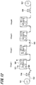
- the roll-to-roll organic functional layer production line shown in FIG. 12 is a first film-forming step Stage 1 in which a substrate laminated roll 501 having an anode or the like is fed out from an unwinder section and passed through a dancer roll section 506.
- a first organic functional layer for example, an electron injection layer is formed on the substrate 502 that is continuously transported while being held by the back roll 505 using a die coater Co that is a coating unit.
- the organic functional layer is similarly applied and dried to form a film in Stage 2 as the next step.
- the substrate 502 on which the organic functional layer group has been formed through Stages 3 and 4 is laminated as a lamination roll 507 in the winder unit through the dancer roll 506.
- PET polyethylene terephthalate film having a thickness of 100 ⁇ m, a width of 200 mm, and a length of 500 m was prepared.
- the alignment mark attached to the prepared PET is detected, and according to the position of the alignment mark, a 120 nm thick ITO (indium tin oxide) is sputtered on the PET under a vacuum environment condition of 5 ⁇ 10 ⁇ 1 Pa on the mask. A pattern was formed, and 12 mm ⁇ 5 mm anodes having take-out electrodes were continuously formed in 12 rows at regular intervals, and temporarily wound up and stored.
- ITO indium tin oxide
- the substrate 502 formed up to the anode is fed out from the unwinder section, and the hole injection layer coating used in the fabrication of the organic EL element 102 is applied in Stage 1 by using the slit type die coater Co shown in FIG.
- the liquid 1 is applied onto the substrate 502 held by the back roll 505, the coating speed is 5 m / min, the coating width is 180 mm, the coater gap is 200 ⁇ m with respect to the wet film thickness, and the temperature at the time of coating the hole injection layer forming coating liquid is 25 ° C.
- a hot injection air of 120 ° C. was blown to form a hole injection layer having a thickness of 30 nm.
- this ITO transparent electrode A substrate P (also referred to as an ITO substrate) provided with an anode) was ultrasonically cleaned with isopropyl alcohol, dried with dry nitrogen gas, and subjected to UV ozone cleaning for 5 minutes.
- the substrate P on which the ITO transparent electrode is formed as the anode is placed on the substrate holding belt 32 that is continuously conveyed, and in the Stage 1 shown in FIG. 2, a slit type die coater Co1 having the configuration shown in FIG. 3 is used.
- the coating speed was set to 3 m / min
- the temperature at the time of coating the hole injection layer forming coating liquid was set to 25 ° C.
- the hole injection layer L1 was applied under the condition that the film thickness was 30 nm, and then heated hot air at 120 ° C. was blown in the drying unit H1 disposed downstream to form the hole injection layer L1.
- the substrate P on which the hole injection layer L1 is formed is transferred to the Stage 2 shown in FIG. 2, and the holes used in the production of the organic EL element 102 using the slit type die coater Co2 having the configuration shown in FIG.
- the transport layer coating liquid 1 is used, the coating speed is 3 m / min, the temperature at the time of coating the hole transport layer forming coating liquid is set to 25 ° C., and the thickness of the hole transport layer L2 after drying is 30 nm.
- a heated hot air of 120 ° C. was blown in the drying unit H2 disposed downstream to form the hole transport layer L2.
- formation of the positive hole transport layer L2 in the 1st film forming environment 30 was performed in the atmosphere 31 of oxygen concentration 300ppm and water concentration 300ppm using nitrogen gas as an inert gas.
- the substrate P on which the hole transport layer L2 is formed is transferred to the Stage 3 shown in FIG. 2, and the light emitting layer used in the production of the organic EL element 102 using the slit type die coater Co3 having the configuration shown in FIG.
- the coating speed was set to 3 m / min
- the temperature at the time of coating the coating liquid for forming the light emitting layer was set to 25 ° C.
- the coating was performed under the condition that the thickness of the light emitting layer L3 after drying was 30 nm. Heating hot air of 120 ° C. was blown at the drying unit H3 disposed downstream to form the light emitting layer L3.
- the formation of the light emitting layer L3 in the first film forming environment 30 was performed in an atmosphere 31 with an oxygen concentration of 300 ppm and a moisture concentration of 300 ppm using nitrogen gas as an inert gas.
- the substrate P on which the light emitting layer L3 is formed is transferred to the Stage 4 shown in FIG. 2, and the electron transport layer coating used in the production of the organic EL element 102 is performed using the slit type die coater Co4 having the configuration shown in FIG.
- the coating speed was 3 m / min
- the temperature at the time of coating the coating liquid for forming the electron transport layer was set to 25 ° C.
- the coating was performed under the condition that the thickness of the electron transport layer L4 after drying was 30 nm.
- a heated hot air of 120 ° C. was blown at the drying unit H4 disposed downstream to form the electron transport layer L4.
- the formation of the electron transport layer L4 in the first film-forming environment 30 was performed in an atmosphere 31 having an oxygen concentration of 300 ppm and a water concentration of 300 ppm using nitrogen gas as an inert gas.
- the second film-forming environment 40 (area 2) during the baking treatment was performed in an atmosphere 41 using nitrogen gas as an inert gas and having an oxygen concentration of 90 ppm and a water concentration of 90 ppm.
- the substrate P formed up to the baked electron injection layer, electron transport layer, light emitting layer, and electron transport layer was attached to a vacuum deposition apparatus without being exposed to the atmosphere.
- a molybdenum resistance heating boat in a vacuum vapor deposition apparatus containing sodium fluoride and potassium fluoride is attached to the vacuum vapor deposition apparatus, and the vacuum chamber is depressurized to 4 ⁇ 10 ⁇ 5 Pa. Heated by energization to form a thin film with a thickness of 1 nm on the electron transport layer at a rate of 0.02 nm / second with sodium fluoride, and then similarly form a film with potassium fluoride at a rate of 0.02 nm / second on the sodium fluoride. A 1.5 nm thick thin film was formed to obtain an electron injection layer. Subsequently, 100 nm of aluminum was vapor-deposited to form a cathode, and an organic EL element 104 was produced.
- Relative investment cost of manufacturing equipment applied to manufacture of organic EL element is less than 0.90
- B Relative investment cost of manufacturing equipment applied to manufacture of organic EL element is 0.90 or more
- 1.10 ⁇ The relative investment cost of the manufacturing equipment applied to the production of the organic EL element is 1.10 or more and less than 1.50
- the relative investment cost of the production equipment applied to the production of the organic EL element is 1.50 or more ⁇
- Quality evaluation of organic EL element >> [Measurement of quantum efficiency]
- the external extraction quantum efficiency when applying a constant current of 2.5 mA / cm 2 in a dry nitrogen gas atmosphere at 23 ° C.
- the quantum efficiency was expressed as a relative value with the quantum efficiency of the organic EL element 104 as 100. It represents that it is excellent in external extraction quantum efficiency, so that a numerical value is large.
- Table 1 shows the results obtained as described above.
- the organic EL device manufacturing method defined in the present invention is an organic device that can achieve both production efficiency and capital investment cost compared to conventional manufacturing methods. It can be seen that the EL element is excellent in quantum efficiency, light emission lifetime and luminance unevenness resistance.
- Example 2 Preparation of organic EL elements 201 to 203 >>
- the application speed in the first film-forming environment 30 (area 1) is 5 m.
- Organic EL elements 201 to 203 were produced in the same manner except for changing to 10 / min, 10 m / min, and 15 m / min.
- the production efficiency can be improved without impairing the properties such as quantum efficiency, light emission lifetime and luminance unevenness resistance. Can be increased.
- Example 3 Production of organic EL elements 301 to 309 >> Organic EL element 105 described in Example 1 (first film forming environment (area 1): using nitrogen gas as an inert gas, in an atmosphere having an oxygen concentration of 300 ppm and a water concentration of 300 ppm. Second film forming environment (area 2): Using nitrogen gas as an inert gas, in an atmosphere having an oxygen concentration of 90 ppm and a moisture concentration of 90 ppm), the atmosphere composition in the first film-forming environment (area 1) and the second film-forming environment (area 2) Organic EL elements 301 to 309 were fabricated in the same manner except that the atmospheric composition was changed to the conditions shown in Table 3, respectively.
- A The relative production cost of the organic EL element is 1.05 or more.
- O The relative production cost of the organic EL element is 0.95 or more and less than 1.05.
- ⁇ The relative production cost of the organic EL element is 0.90 or more and less than 0.95 ⁇ : The relative production cost of the organic EL element is less than 0.90
- the concentration of gas components other than the inert gas in the first film-forming environment (area 1) is 500 ppm or more, and other than the inert gas in the second film-forming environment (area 2) It can be seen that by making the gas component concentration of 200 ppm or less, the production cost is excellent and the quantum efficiency, the light emission lifetime, and the luminance unevenness resistance are further improved.
- Example 4 Preparation of organic EL elements 401 to 408 >>
- the type of the substrate resin substrate: polyethylene terephthalate film having a thickness of 100 ⁇ m
- Glass substrate made of NH technoglass with a thickness of 1.1 mm, NA45
- EL elements 401 to 408 were produced.
- the production efficiency is higher than that of an organic EL element using a resin substrate, and the baking time in the second film-forming environment (area 2). It can be seen that even if the length is shortened, the performance degradation is small. This is because the glass substrate has less penetration of the solvent or the like constituting each coating liquid into the substrate when the organic functional layer is applied, and as a result, the glass substrate is desired even in a short time. It is speculated that the characteristics of
- Example 5 [Production of Organic EL Element 502]
- the substrate was not lifted by the substrate floating portion 55, but was directly placed on the substrate holding member and applied to produce the organic EL element 502. .
- Alignment marks were given to the four corners of a glass substrate P of 150 mm ⁇ 150 mm ⁇ 1.1 mm.
- the alignment marks were formed by forming a cross mark with an ITO (indium tin oxide) film having a thickness of 120 nm at the four corners on the glass substrate P under a vacuum environment condition of 5 ⁇ 10 ⁇ 1 Pa by a sputtering method.
- ITO indium tin oxide
- this ITO transparent electrode A substrate P (also referred to as an ITO substrate) provided with an anode) was ultrasonically cleaned with isopropyl alcohol, dried with dry nitrogen gas, and subjected to UV ozone cleaning for 5 minutes.
- the substrate P on which the ITO transparent electrode is formed as the anode is placed on the substrate holding member 32 that is continuously transported, and in the Stage 1 shown in FIG. 4, a slit type die coater Co1 having the configuration shown in FIG. 6 is used.
- the alignment mark is detected by a CCD camera, and according to the information, the hole injection layer coating solution 1 used in the production of the organic EL element 102 on the substrate P is applied at a coating speed of 3 m / min, with a coating speed of 3 m / min.
- coating of the coating liquid for hole injection layer formation is set to 25 degreeC, it apply
- the hole injection layer L1 was formed by spraying 120 ° C. hot air.
- the substrate P on which the hole injection layer L1 is formed is transferred to the Stage 2 shown in FIG. 4, and the holes used in the production of the organic EL element 102 are made using the slit type die coater Co2 having the configuration shown in FIG.
- the transport layer coating liquid 1 according to the detection information of the alignment mark by the CCD camera, set the coating speed to 3 m / min, and the temperature during coating of the hole transport layer forming coating liquid to 25 ° C. without floating the substrate at all.
- the hole transport layer L2 after drying is applied under the condition that the film thickness is 30 nm, and then heated hot air at 120 ° C. is blown in the drying unit H2 disposed downstream to form the hole transport layer L2. did.
- formation of the positive hole transport layer L2 in the 1st film forming environment 30 was performed in the atmosphere 31 of oxygen concentration 300ppm and water concentration 300ppm using nitrogen gas as an inert gas.
- the substrate P on which the hole transport layer L2 is formed is transferred to the Stage 3 shown in FIG. 4, and the light emitting layer used in the production of the organic EL element 102 using the slit type die coater Co3 having the configuration shown in FIG.
- the coating solution 1 according to the alignment mark detection information by the CCD camera, the substrate is not lifted at all, the substrate is not lifted at all, the coating speed is 3 m / min, and the temperature at the time of coating the coating solution for forming the light emitting layer is 25 ° C.
- the light emitting layer L3 after drying was coated under the condition that the film thickness was 30 nm, and then heated warm air at 120 ° C. was blown in the drying unit H3 disposed downstream to form the light emitting layer L3. .
- the formation of the light emitting layer L3 in the first film forming environment 30 was performed in an atmosphere 31 having an oxygen concentration of 300 ppm and a water concentration of 300 ppm using nitrogen gas as an inert gas.
- the substrate P on which the light emitting layer L3 is formed is transferred to the Stage 4 shown in FIG. 4, and the slit-type die coater Co4 having the configuration shown in FIG. 6 is used to apply the electron transport layer used in the production of the organic EL element 102.
- the coating speed was set to 3 m / min, and the temperature at the time of coating the coating liquid for forming the electron transport layer was set to 25 ° C.
- the electron transport layer L4 was applied under the condition that the film thickness was 30 nm, and then heated warm air of 120 ° C. was blown at the drying unit H4 disposed downstream to form the electron transport layer L4.
- the formation of the electron transport layer L4 in the first film-forming environment 30 was performed in an atmosphere 31 having an oxygen concentration of 300 ppm and a water concentration of 300 ppm using nitrogen gas as an inert gas.
- the second film-forming environment 40 (area 2) during the baking treatment was performed in an atmosphere 41 using nitrogen gas as an inert gas and having an oxygen concentration of 90 ppm and a water concentration of 90 ppm.
- the substrate P formed up to the baked electron injection layer, electron transport layer, light emitting layer, and electron transport layer was attached to a vacuum deposition apparatus without being exposed to the atmosphere.
- a molybdenum resistance heating boat in a vacuum vapor deposition apparatus containing sodium fluoride and potassium fluoride is attached to the vacuum vapor deposition apparatus, and the vacuum chamber is depressurized to 4 ⁇ 10 ⁇ 5 Pa. Heated by energization to form a thin film with a thickness of 1 nm on the electron transport layer at a rate of 0.02 nm / second with sodium fluoride, and then similarly form a film with potassium fluoride at a rate of 0.02 nm / second on the sodium fluoride. A 1.5 nm thick thin film was formed to obtain an electron injection layer. Subsequently, 100 nm of aluminum was deposited to form a cathode, and an organic EL element 502 was produced.
- Alignment marks were given to the four corners of a glass substrate P of 150 mm ⁇ 150 mm ⁇ 1.1 mm.
- the alignment marks were formed by forming a cross mark with an ITO (indium tin oxide) film having a thickness of 120 nm at the four corners on the glass substrate P under a vacuum environment condition of 5 ⁇ 10 ⁇ 1 Pa by a sputtering method.
- ITO indium tin oxide
- this ITO transparent electrode A substrate P (also referred to as an ITO substrate) provided with an anode) was ultrasonically cleaned with isopropyl alcohol, dried with dry nitrogen gas, and subjected to UV ozone cleaning for 5 minutes.
- the substrate P on which the ITO transparent electrode is formed as the anode is placed on the substrate holding member 32 that is continuously transported, and in the Stage 1 shown in FIG. 4, a slit type die coater Co1 having the configuration shown in FIG. 6 is used.
- the alignment mark was detected by the CCD camera, and the substrate P was floated by the substrate floating portion shown in FIG. 7 according to the obtained positional information of the substrate.
- two compressed gas supply units 300A and 300B were supplied with compressed gas having an inert gas of nitrogen gas, an oxygen concentration of 300 ppm, and a moisture concentration of 300 ppm by gas blow pumps 304A and 304B.
- the vacuum pump 305 was operated to take in air from the decompression unit 306.
- the flying height H1 of the substrate P with respect to the substrate holding member 32 is controlled to 150 ⁇ m by the position detection sensor 307, and the height H2 (bead gap) between the lip at the tip of the coating coater Co and the surface of the substrate P is 300 ⁇ m. Furthermore, the amount of compressed gas blown and the amount of intake air were controlled by the decompression unit 306.
- the hole injection layer coating liquid 1 used in the production of the organic EL element 102 on the substrate P was applied at a coating speed of 3 m / min, and the temperature during coating of the hole injection layer forming coating liquid was 25 ° C. Set and apply under the condition that the film thickness of the hole injection layer L1 after drying is 30 nm, and then spray heated hot air at 120 ° C. in the drying unit H1 disposed downstream, and the hole injection layer L1 Formed.
- the substrate P on which the hole injection layer L1 is formed is transferred to the Stage 2 shown in FIG. 4, and the holes used in the production of the organic EL element 102 are made using the slit type die coater Co2 having the configuration shown in FIG.
- the transport layer coating solution 1 the substrate was floated at a height of 150 ⁇ m in the same manner as the floating condition of the hole injection layer, while applying a coating speed of 3 m / min at the time of coating the hole transport layer forming coating solution.
- the temperature was set to 25 ° C., and the coating was performed under the condition that the film thickness of the hole transport layer L2 after drying was 30 nm, and then heated hot air of 120 ° C. was blown at the drying unit H2 disposed downstream, A hole transport layer L2 was formed.
- formation of the positive hole transport layer L2 in the 1st film forming environment 30 was performed in the atmosphere 31 of oxygen concentration 300ppm and water concentration 300ppm using nitrogen gas as an inert gas.
- the substrate P on which the hole transport layer L2 is formed is transferred to the Stage 3 shown in FIG. 4, and the light emitting layer used in the production of the organic EL element 102 using the slit type die coater Co3 having the configuration shown in FIG.
- the coating speed was 3 m / min
- the temperature at the time of coating the light emitting layer forming coating liquid was 25 ° C.
- the light emitting layer L3 after drying was coated under the condition that the film thickness was 30 nm, and then heated warm air at 120 ° C. was blown in the drying unit H3 disposed downstream to form the light emitting layer L3. .
- the formation of the light emitting layer L3 in the first film forming environment 30 was performed in an atmosphere 31 with an oxygen concentration of 300 ppm and a moisture concentration of 300 ppm using nitrogen gas as an inert gas.
- the substrate P on which the light emitting layer L3 is formed is transferred to the Stage 4 shown in FIG. 4, and the slit-type die coater Co4 having the configuration shown in FIG. 6 is used to apply the electron transport layer used in the production of the organic EL element 102.
- the coating speed was 3 m / min, and the temperature at the time of coating the coating liquid for forming the electron transport layer was 25 ° C.
- the electron transport layer L4 after drying is applied under the condition that the film thickness is 30 nm, and then heated warm air of 120 ° C. is blown in the drying unit H4 disposed downstream to thereby form the electron transport layer L4. Formed.
- the formation of the electron transport layer L4 in the first film-forming environment 30 was performed in an atmosphere 31 having an oxygen concentration of 300 ppm and a water concentration of 300 ppm using nitrogen gas as an inert gas.
- the second film-forming environment 40 (area 2) during the baking treatment was performed in an atmosphere 41 using nitrogen gas as an inert gas and having an oxygen concentration of 90 ppm and a water concentration of 90 ppm.
- the substrate P formed up to the baked electron injection layer, electron transport layer, light emitting layer, and electron transport layer was attached to a vacuum deposition apparatus without being exposed to the atmosphere.
- a molybdenum resistance heating boat in a vacuum vapor deposition apparatus containing sodium fluoride and potassium fluoride is attached to the vacuum vapor deposition apparatus, and the vacuum chamber is depressurized to 4 ⁇ 10 ⁇ 5 Pa.
- a current is applied and heated to form a thin film with a thickness of 1 nm on the electron transport layer at a rate of 0.02 nm / second with sodium fluoride, and then similarly with potassium fluoride at a rate of 0.02 nm / second on the sodium fluoride.
- a 1.5 nm thick thin film was formed to obtain an electron injection layer.
- 100 nm of aluminum was deposited to form a cathode, and an organic EL element 503 was produced.
- the constituent solvent of the organic functional layer coating liquid used in each Stage was used as the cleaning liquid in each Stage.
- the constituent solvent of the organic functional layer coating liquid used in each Stage was used as the cleaning liquid in each Stage.
- ⁇ Quality evaluation of organic EL elements >> [Evaluation of luminance unevenness resistance: Evaluation of film surface uniformity] The luminance distribution in the light emitting surface when a constant current of 2.5 mA / cm 2 was applied to each of the produced organic EL elements was measured with Prometric (manufactured by Cybernet System). The luminance distribution was expressed as the standard deviation of the luminance within each light emitting surface when the light emitting surface was equally divided into 40. The lower the numerical value, the less the luminance unevenness and the better the luminance unevenness resistance.
- the organic EL device manufacturing method defined in the present invention is superior in production efficiency to the conventional manufacturing method and excellent in luminance unevenness resistance of the manufactured organic EL device.
- the formation of the organic functional layer while being floated and conveyed suppresses the generation of dark spots due to dust and the like.
- Example 6 Preparation of organic EL elements 601 to 609 >> Organic EL element 505 described in Example 5 (first film forming environment (area 1): using nitrogen gas as an inert gas, in an atmosphere having an oxygen concentration of 300 ppm and a water concentration of 300 ppm. Second film forming environment (area 2): In the production of nitrogen gas as an inert gas and in an atmosphere having an oxygen concentration of 90 ppm and a moisture concentration of 90 ppm), the atmosphere composition in the first film-forming environment (area 1) and the second film-forming environment (area 2) Organic EL elements 601 to 609 were produced in the same manner except that the atmospheric composition in (1) was changed to the conditions shown in Table 6.
- the concentration of gas components other than the inert gas in the first film-forming environment (area 1) is 500 ppm or more, and other than the inert gas in the second film-forming environment (area 2) It can be seen that the brightness unevenness resistance and the dark spot resistance are further improved by setting the gas component concentration of 200 ppm or less.
Landscapes
- Engineering & Computer Science (AREA)
- Manufacturing & Machinery (AREA)
- Electroluminescent Light Sources (AREA)
- Application Of Or Painting With Fluid Materials (AREA)
Abstract
生産効率(高生産性、低設備コスト)が高く、量子効率、発光寿命及び輝度ムラ耐性に優れた有機エレクトロルミネッセンス素子が得られる有機エレクトロルミネッセンス素子の製造方法を提供する。 枚葉形態の基板上に、少なくとも2層の有機機能層を、ダイコート法によりインライン方式で連続積層塗布して有機エレクトロルミネッセンス膜を形成することを特徴とする有機エレクトロルミネッセンス素子の製造方法。
Description
本発明は、均一な膜厚で高品位な有機機能膜を得ることができ、更には高い生産性でありながら、設備費用を低く抑えられる有機エレクトロルミネッセンス素子の製造方法に関するものである。
従来、有機エレクトロルミネッセンス素子(以下、有機ELともいう)は、蒸着方式を用いた製膜法により製造されているが、生産性の向上や製造コスト低減のため、近年では、湿式塗布方式を適用した製造方式の開発が望まれている。また、有機エレクトロルミネッセンス素子の各構成層を、湿式塗布方式により形成する場合、各構成層の形成に用いる塗布液の粘度は非常に低く、塗布膜厚も非常に薄いため、均一な膜厚を有する層の形成が強く要望されている。
薄層形成に適用される塗布方式の1つとして、スピンコート法が知られている。スピンコート法は、薄膜形成用塗布液を基板上に滴下した後、支持体を回転させて遠心力により支持体全面に塗布を行って薄膜を形成する方法であり、回転数、回転時間、あるいは塗布液の粘度等により膜厚を制御するものである。スピンコート法は、例えば半導体製造工程等に用いられるフォトレジスト膜やSOG(スピンオンガラス)等の層間絶縁膜の形成、液晶装置製造工程等におけるオーバーコート膜(平坦膜)や配向膜の形成、さらには光ディスク等の製造工程における保護膜の形成等に広く用いられている。
しかしながら、スピンコート法は、膜厚精度は高いものの、支持体を回転させる必要があるため、帯状支持体に連続して塗布することができない。このため、切断した支持体を毎回取り替えながら塗布する必要があり、また塗布の際に支持体の端部からはみ出す塗布液の量が多く、生産コストが高くなるという問題がある。
また、他の薄膜塗布法としては、インクジェット方式も知られているが、インクジェット方式では塗布速度が遅く生産性が低いという問題がある。
一方、フレキソ印刷方式は、連続生産が可能で高速塗布に有効な方式として知られている。しかしながら、液晶装置や有機EL装置等のディスプレイ装置に用いられるディスプレイ材料の塗布膜は、要求される膜厚精度が高く、フレキソ印刷方式で作成した塗布膜では要求される膜厚精度や塗布品質が得られないという問題がある。
このため、フレキソ印刷方式で塗布ムラを抑制するために、版材の全面に均等に凹凸を設けたものを用いて、版材の凹部に充填された塗布液を支持体に転写させる塗布方法が特許文献1に記載されているものの、ディスプレイ材料の塗布膜に要求される膜厚精度や塗布品質を満足するには十分でなかった。
更に、スリット型ダイコータを用いたエクストルージョン塗布法も塗布精度の高さ、高速、薄膜、多層塗布適性等の対応が可能であることから検討されており、例えばロールツーロール方式で連続塗布する方法が特許文献2に記載されている。しかし、ロールツーロール方式は、生産性としては高いものの、生産ライン設備が複雑で投資費用が膨大になるため、均一な膜厚の塗布膜を得ることができ、更には高い生産性でありながら、設備費用を低く抑えられる製造方法が求められていた。
一方、大型で枚葉の基板の搬送手段として、一般にベルトコンベア、ローラコンベア等が広く用いられるが、製造ラインにおける搬送や移載の際に、基板と搬送手段との接触等により基板が傷つき、更には接触による細かな微粉が基板表面に付着してダークスポットになる上に、振動により塗布スジが発生してしまうことが判明した。そこで、多孔質板から噴き出すエア圧で浮上させながら搬送させる方法が、例えば、特許文献3に記載されているものの、その効果は十分であるとは言い難いのが現状である。
本発明は、上記課題に鑑みなされたものであり、その目的は、生産効率(高生産性、低設備コスト)が高く、量子効率、発光寿命及び輝度ムラ耐性に優れた有機エレクトロルミネッセンス素子が得られる有機エレクトロルミネッセンス素子の製造方法を提供することにある。
さらに、本発明の目的は、高い生産性を有し、塗膜の均一性が高く、ダークスポット等の塗布故障が低減した高品位の有機機能膜を得ることができる有機エレクトロルミネッセンス素子の製造方法を提供することにある。
さらに、本発明の目的は、高い生産性を有し、塗膜の均一性が高く、ダークスポット等の塗布故障が低減した高品位の有機機能膜を得ることができる有機エレクトロルミネッセンス素子の製造方法を提供することにある。
本発明の上記目的は、以下の構成により達成される。
1.枚葉形態の基板上に、少なくとも2層の有機機能層を、ダイコート法によりインライン方式で連続積層塗布して有機エレクトロルミネッセンス膜を形成することを特徴とする有機エレクトロルミネッセンス素子の製造方法。
2.前記なくとも2層の有機機能層が、不活性ガスを除く気体の体積濃度が500ppm以上の第1の雰囲気(エリア1)で連続積層塗布された後、不活性ガスを除く気体の体積濃度が200ppm以下の第2の雰囲気(エリア2)で加熱乾燥処理を施すことを特徴とする前記1に記載の有機エレクトロルミネッセンス素子の製造方法。
3.前記少なくとも2層の有機機能層が、塗布速度5m/min以上で積層塗布されることを特徴とする前記1または2に記載の有機エレクトロルミネッセンス素子の製造方法。
4.前記第1の雰囲気(エリア1)及び第2の雰囲気(エリア2)を構成する不活性ガスが、窒素ガスであることを特徴とする前記2または3に記載の有機エレクトロルミネッセンス素子の製造方法。
5.前記第1の雰囲気(エリア1)及び第2の雰囲気(エリア2)を構成する不活性ガスを除く気体が、水分及び酸素ガスであることを特徴とする前記2から4のいずれか1項に記載の有機エレクトロルミネッセンス素子の製造方法。
6.前記枚葉形態の基板が、ガラス基板であることを特徴とする前記1から5のいずれか1項に記載の有機エレクトロルミネッセンス素子の製造方法。
7.枚葉形態の基板上に、少なくとも2層の有機機能層を、ダイコータを用いてインライン方式で連続積層塗布して有機機能層積層体を形成する有機エレクトロルミネッセンス素子の製造方法であって、該基板を基板浮上ユニットで保持し、該基板浮上ユニットは、気体の吹き出し部と、気体の吸引部とを有し、該気体の吹き出し量と吸引量を制御して、前記基板を浮上させながら前記ダイコータにより塗布して有機機能層積層体を形成することを特徴とする有機エレクトロルミネッセンス素子の製造方法。
8.前記枚葉形態の基板上に1つの有機機能層を塗布した後に、それぞれ独立した乾燥ゾーンを有していることを特徴とする前記7に記載の有機エレクトロルミネッセンス素子の製造方法。
9.前記少なくとも2層の有機機能層を塗布する第1の雰囲気(エリア1)が、不活性ガスを除く気体の体積濃度が500ppm以上の雰囲気であることを特徴とする前記7または8に記載の有機エレクトロルミネッセンス素子の製造方法。
10.前記基板浮上ユニットの吹き出し部より供給する浮上用気体が、不活性ガスを除く気体の体積濃度が500ppm以上の気体であることを特徴とする前記7から9のいずれか1項に記載の有機エレクトロルミネッセンス素子の製造方法。
11.前記少なくとも2層の有機機能層をダイコータによりインライン方式で連続積層塗布した有機機能層積層体に、不活性ガスを除く気体の体積濃度が200ppm以下の第2の雰囲気(エリア2)で加熱乾燥処理を施すことを特徴とする前記7から10のいずれか1項に記載の有機エレクトロルミネッセンス素子の製造方法。
12.前記第1の雰囲気(エリア1)、基板浮上ユニットの吹き出し部より供給する浮上用気体及び第2の雰囲気(エリア2)を構成する不活性ガスが、窒素ガスであることを特徴とする前記9から11のいずれか1項に記載の有機エレクトロルミネッセンス素子の製造方法。
13.前記第1の雰囲気(エリア1)、基板浮上ユニットの吹き出し部より供給する浮上用気体及び第2の雰囲気(エリア2)を構成する不活性ガスを除く気体が、水分及び酸素ガスであることを特徴とする前記9から12のいずれか1項に記載の有機エレクトロルミネッセンス素子の製造方法。
14.前記枚葉形態の基板上に形成する有機機能層が、パターン状であることを特徴とする前記7から13のいずれか1項に記載の有機エレクトロルミネッセンス素子の製造方法。
15.前記枚葉形態の基板上にアライメントマークを設け、該アライメントマークを検知して、前記ダイコータから該枚葉形態の基板上への有機機能層形成用塗布液の供給及び停止を制御することを特徴とする前記7から14のいずれか1項に記載の有機エレクトロルミネッセンス素子の製造方法。
16.前記ダイコータへの有機機能層形成用塗布液の停止時期に、該ダイコータのリップ部にワイピング洗浄処理を施すことを特徴とする前記7から15のいずれか1項に記載の有機エレクトロルミネッセンス素子の製造方法。
17.前記枚葉形態の基板が、ガラス基板であることを特徴とする前記7から16のいずれか1項に記載の有機エレクトロルミネッセンス素子の製造方法。
本発明により、生産効率(高生産性、低設備コスト)が高く、量子効率、発光寿命及び輝度ムラ耐性に優れた有機エレクトロルミネッセンス素子が得られる有機エレクトロルミネッセンス素子の製造方法を提供することができた。
本発明において、さらに、基板を基板浮上ユニットで保持し、基板浮上ユニットは、気体の吹き出し部と、気体の吸引部とを有し、気体の吹き出し量と吸引量を制御して、基板を浮上させながらダイコータにより塗布して有機機能層積層体を形成する構成とすることにより、高い生産性を有し、塗膜の均一性が高く、ダークスポット等の塗布故障が低減した高品位の有機機能膜を得ることができる有機エレクトロルミネッセンス素子の製造方法を提供することができた。
以下、本発明を実施するための形態について詳細に説明する。
本発明者は、上記課題に鑑み鋭意検討を行った結果、枚葉形態の基板上に、少なくとも2層の有機機能層を、ダイコート法によりインライン方式で連続積層塗布して有機エレクトロルミネッセンス膜を形成することを特徴とする有機エレクトロルミネッセンス素子の製造方法により、生産効率(高生産性、低設備コスト)が高く、量子効率、発光寿命及び輝度ムラ耐性に優れた有機エレクトロルミネッセンス素子が得られる有機エレクトロルミネッセンス素子の製造方法を実現できることを見出し、本発明に至った次第である。
また、本発明者は、枚葉形態の基板上に、少なくとも2層の有機機能層を、ダイコータを用いてインライン方式で連続積層塗布して有機機能層積層体を形成する有機エレクトロルミネッセンス素子の製造方法であって、該基板を基板浮上ユニットで保持し、該基板浮上ユニットは、気体の吹き出し部と、気体の吸引部とを有し、該気体の吹き出し量と吸引量を制御して、前記基板を浮上させながら前記ダイコータにより塗布して有機機能層積層体を形成することを特徴とする有機エレクトロルミネッセンス素子の製造方法により、高い生産性を有し、塗膜の均一性が高く、ダークスポット等の塗布故障が低減した高品位の有機機能膜を得ることができる有機エレクトロルミネッセンス素子の製造方法を実現できることを見出した。
以下、本発明の有機エレクトロルミネッセンス素子の製造方法について、その詳細を説明する。
《有機EL素子の基本的な構成》
図1に、本発明に係る有機EL素子の基本的な構成の一例を示す。
図1に、本発明に係る有機EL素子の基本的な構成の一例を示す。
図1において、有機EL素子1は、支持基板Pを有している。支持基板P上には陽極2が形成され、陽極2上には、複数の有機機能層から構成される有機機能層群20が形成され、有機機能層群20上には陰極8が形成されている。
有機機能層群20とは、陽極2と陰極8との間に設けられている有機EL素子1を構成する各有機機能層から構成されている。
有機機能層群20を構成する各有機機能層としては、例えば、正孔注入層3、正孔輸送層4、発光層5、電子輸送層6、電子注入層7が含まれ、そのほかに正孔ブロック層や電子ブロック層等が含まれてもよい。
支持基板P上の陽極2、有機機能層20、陰極8は、封止接着剤9を介して可撓性封止部材10によって封止されている。
なお、有機EL素子1のこれらの層構造(図1参照)は単に好ましい具体例を示したものであり、本発明はこれらに限定されない。
例えば、本発明に係る有機EL素子1の構成としては、下記に示す(i)~(viii)の層構造を有していてもよい。
(i)支持基板/陽極/発光層/電子輸送層/陰極/熱伝導層/封止用接着剤/封止部材
(ii)支持基板/陽極/正孔輸送層/発光層/電子輸送層/陰極/熱伝導層/封止用接着剤/封止部材
(iii)支持基板/陽極/正孔輸送層/発光層/正孔ブロック層/電子輸送層/陰極/熱伝導層/封止用接着剤/封止部材
(iv)支持基板/陽極/正孔輸送層/発光層/正孔ブロック層/電子輸送層/陰極バッファー層/陰極/熱伝導層/封止用接着剤/封止部材
(v)支持基板/陽極/陽極バッファー層/正孔輸送層/発光層/正孔ブロック層/電子輸送層/陰極バッファー層/陰極/熱伝導層/封止用接着剤/封止部材
また、基板としては、上記支持基板に代えて、ガラス支持体を用いることもできる。
(ii)支持基板/陽極/正孔輸送層/発光層/電子輸送層/陰極/熱伝導層/封止用接着剤/封止部材
(iii)支持基板/陽極/正孔輸送層/発光層/正孔ブロック層/電子輸送層/陰極/熱伝導層/封止用接着剤/封止部材
(iv)支持基板/陽極/正孔輸送層/発光層/正孔ブロック層/電子輸送層/陰極バッファー層/陰極/熱伝導層/封止用接着剤/封止部材
(v)支持基板/陽極/陽極バッファー層/正孔輸送層/発光層/正孔ブロック層/電子輸送層/陰極バッファー層/陰極/熱伝導層/封止用接着剤/封止部材
また、基板としては、上記支持基板に代えて、ガラス支持体を用いることもできる。
(vi)ガラス支持体/陽極/正孔注入層/発光層/電子注入層/陰極/封止部材
(vii)ガラス支持体/陽極/正孔注入層/正孔輸送層/発光層/電子注入層/陰極/封止部材
(viii)ガラス支持体/陽極/正孔注入層/正孔輸送層/発光層/電子輸送層/電子注入層/陰極/封止部材
《有機EL素子の製造方法》
次いで、本発明の有機EL素子の製造方法について、図を交えてその詳細を説明する。
(vii)ガラス支持体/陽極/正孔注入層/正孔輸送層/発光層/電子注入層/陰極/封止部材
(viii)ガラス支持体/陽極/正孔注入層/正孔輸送層/発光層/電子輸送層/電子注入層/陰極/封止部材
《有機EL素子の製造方法》
次いで、本発明の有機EL素子の製造方法について、図を交えてその詳細を説明する。
本発明の有機EL素子の製造方法では、枚葉形態の基板上に、少なくとも2層の有機機能層を、ダイコート法によりインライン方式で、湿式塗布液を用いて、連続積層塗布して有機機能層群を形成することを特徴とする。
図2は、本発明の有機EL素子の製造方法に適用可能な製造工程の一例を示す工程フロー図であり、図2に示すフローに従って本発明に係る有機EL素子を製造することができる。
図2に示すように、矢印方向に移動している基板保持部材(基板保持ベルト)32上に、所望のサイズに断裁した枚葉形態の基板Pを一定間隔で配置する。第1の塗布工程であるStage1で、例えば、図1に示す構成の有機EL素子においては、陽極2まで形成した基板P上に、第1のダイコータCo1を用いて、第1の有機機能層L1、例えば、図1の構成で示す正孔注入層3を、ダイコート法により湿式塗布方式で形成する。基板P上に形成した第1の有機機能層L1(例えば、正孔注入層3)は、紙面の右側に移送され、必要に応じて乾燥部H1にて有機溶媒等の除去が行われる。次いで、基板Pは、第2の塗布工程であるStage2に移送される。Stage2では、第1の有機機能層L1を形成した基板P上に、第2のダイコータCo2を用い、第2の有機機能層L2として、例えば、図1の構成で示す正孔輸送層4を、ダイコート法により湿式塗布方式で形成する。基板P上に形成した第2の有機機能層L2(例えば、正孔輸送層4)は、紙面の右側に移送され、必要に応じて乾燥部H2にて乾燥される。
同様にして、第3の塗布工程であるStage3で第3の有機機能層L3(例えば、発光層5)を、第4の塗布工程であるStage4で第4の有機機能層L4(例えば、電子輸送層6)を、枚葉基板P上にオンラインで形成する。
次いで、有機機能層群20を形成した枚葉の基板Pは、オフラインで雰囲気条件の異なるエリア2(40)に移送し、ここで特定の雰囲気条件下で加熱処理(ベイク処理)により、最終乾燥を行う。
次いで、乾燥処理が施された有機機能層群20を形成した枚葉の基板Pは、蒸着工程50、例えば、真空蒸着装置51内に移送され、蒸着源52より所望の構成材料を蒸着させて、電子注入層7や陰極8が形成される。
陰極8を形成した後、封止工程にて、封止接着剤9を介して可撓性封止部材10によって封止して、有機EL素子が製造される。
上記一連の有機EL素子の製造フローにおいて、第1の製膜環境30(エリア1、Stage1~4)における乾燥部H1~H4での乾燥は行わずに、第2の製膜環境40(エリア2)で一括乾燥を行っても良い。
図4は、本発明の有機EL素子の製造方法に適用可能な製造方法の他の一例として、基板浮上ユニットを備えた製造工程の一例を示す工程フロー図であり、図4に示すフローに従って本発明に係る有機EL素子を製造することができる。なお、図4において、図2と共通する構成には同一符号を付している。
図4に示すように、エリア1(30)では、サポートロール54で保持されながら、搬送ロール53により矢印方向に搬送移動している多孔質構造で気体通気性を有する基板保持部材32上に、所望のサイズに断裁した枚葉形態の基板Pを一定間隔で配置する。第1の塗布工程であるStage1で、例えば、図1に示す構成の有機EL素子においては、陽極2まで形成した基板P上に、第1のダイコータCo1を用いて、第1の有機機能層L1、例えば、図1の構成で示す正孔注入層3を、ダイコート法により湿式塗布方式で形成する。基板P上に形成した第1の有機機能層L1(例えば、正孔注入層3)は、下流側に移送され、必要に応じて、乾燥ゾーンD1の乾燥部H1にて有機溶媒等の除去が行われる。次いで、基板Pは、第2の塗布工程であるStage2に移送される。Stage2では、第1の有機機能層L1を形成した基板P上に、第2のダイコータCo2を用い、第2の有機機能層L2として、例えば、図1の構成で示す正孔輸送層4を、ダイコート法により湿式塗布方式で形成する。基板P上に形成した第2の有機機能層L2(例えば、正孔輸送層4)は、更に下流側に移送され、必要に応じて、乾燥ゾーンD2の乾燥部H2にて乾燥される。
同様にして、第3の塗布工程であるStage3で第3の有機機能層L3(例えば、発光層5)を、第4の塗布工程であるStage4で第4の有機機能層L4(例えば、電子輸送層6)を、枚葉基板P上にオンラインで形成する。
次いで、有機機能層群20を形成した枚葉の基板Pは、オフラインで雰囲気条件の異なるエリア2(40)に移送し、ここで特定の雰囲気条件下で加熱処理(ベイク処理)により、最終乾燥を行う。
次いで、乾燥処理が施された有機機能層群20を形成した枚葉の基板Pは、蒸着工程50、例えば、真空蒸着装置51内に移送され、蒸着源52より所望の構成材料を蒸着させて、電子注入層7や陰極8が形成される。
陰極8を形成した後、封止工程にて、封止接着剤9を介して可撓性封止部材10によって封止して、有機EL素子が製造される。
上記の様な有機EL素子の製造ラインにおいて、各Stageの塗布工程(それぞれダイコータが配置されているポジション)では、搬送されている多孔質構造で気体通気性を有する基板保持部材32の背面部に、基板浮上部55がそれぞれ配置され、ダイコータにより塗布を行う際に、基板浮上部55内に設置された多孔質の基板浮上ユニット56(詳細については、後述する)より基板浮上用の圧縮気体の送風及び真空ポンプによる吸引を行い、基板を一定の高さで制御して浮上させると共に、吸引部で吸引を行うことにより浮上させた基板を基板保持部材32の搬送を同期させて搬送を行う方法である。
本発明に適用可能な基板保持部材32の構造としては、特に制限はないが、背面側に配置している基板浮上ユニット56からの基板浮上用の圧縮気体を安定に、基板に送風できる構造であることが好ましく、例えば、膜厚方向に貫通した空隙構造を有する多孔質構成、あるいは、基板保持部材32面に、一定の間隔で、多数の厚さ方向で貫通している細孔を設けたパンチ板構造であっても良い。また、細孔の配置も厚さ方向に対して垂直方法であっても、あるいは、浮上させる基板の搬送性を加味して、斜め構造、例えば、図4に記載の基板保持部材32では、細孔が右側に傾斜した構造であることが好ましい。
基板保持部材32に固定した状態で基板Pを搬送する場合には、基板保持部材32の搬送時の振動等による変位の影響を受け、固定されているダイコータの底面と基板Pの表面との距離が変動し、その結果、ビード間隙が過度に広くなることによる液切れが発生する恐れがあり、未塗布部を発生させる要因となる。また、ビード間隙が過度に狭くなることにより、塗布スジを発生させる要因となる。加えて、基板保持部材32と基板Pとの搬送時の接触により、基板Pのエッジ部が破損し、発生した粉塵等の付着により、塗布故障を誘発させる恐れがある。
上記課題に対し、本発明の有機EL素子の製造方法においては、基板保持部材32に対し、基板Pを浮上させた状態で塗布することにより、ダイコータの底面と基板Pの表面との距離(ビード間隙ともいう)を一定の範囲に厳密に制御することにより、塗布時の液切れや塗布スジの発生を防止できると共に、非接触搬送により、粉塵等の発生も防止することができる。
図5は、本発明の有機EL素子の製造方法に適用可能で、基板保持部材として無端搬送ベルト59を有する基板浮上ユニット一例を示す工程フロー図であり、図5には、塗布工程であるエリア1(30)のみを記載してある。
図5に示す様に、基板保持部材としてサポートロール54及び搬送ロール53Aで保持された無端搬送ベルト59を搬送させながら、図4に示す方法と同様にして、基板浮上部55内に設置された多孔質の基板浮上ユニット56により、基板浮上用の圧縮気体の基板への送風及び吸引を行うことにより、基板を浮上させながら塗布を行う。
この様な無端搬送ベルト59を基板保持部材として用いる場合には、折り曲げ等に耐久性を有する細孔を多数配列した金属無端ベルトを用いることが好ましい。
上記一連の有機EL素子の製造フローにおいて、第1の製膜環境30(エリア1、Stage1~4)における乾燥部H1~H4での乾燥は行わずに、第2の製膜環境40(エリア2)で一括乾燥を行っても良い。
〔有機機能層群の塗膜形成環境〕
図2、図4に示すような本発明の有機EL素子の製造方法において、例えば、陽極が形成された枚葉の基板P上に、正孔注入層3、正孔輸送層4、発光層5、電子輸送層6、電子注入層7等の有機機能層群20を形成させる工程と、その後工程である乾燥工程における環境(雰囲気)条件としては、主に、
(i)その有機機能層群を構成する各有機機能層塗布液を用い、不活性ガス以外の気体の体積濃度が500ppm以上の第1の雰囲気30(エリア1)で、図2、図4に記載の工程に従って枚葉の基板Pの陽極2上に、ダイコート法によりインライン方式で複数の有機機能層を塗布、積層する工程と、
(ii)第1の雰囲気30(エリア1)で、ダイコート法により各有機機能層を塗布、積層した後の有機機能層群を、オフラインで不活性ガス以外の気体の体積濃度が200ppm以下の第2の雰囲気40(エリア2)で乾燥させる工程(ベーク工程)と、
で構成することができる。
図2、図4に示すような本発明の有機EL素子の製造方法において、例えば、陽極が形成された枚葉の基板P上に、正孔注入層3、正孔輸送層4、発光層5、電子輸送層6、電子注入層7等の有機機能層群20を形成させる工程と、その後工程である乾燥工程における環境(雰囲気)条件としては、主に、
(i)その有機機能層群を構成する各有機機能層塗布液を用い、不活性ガス以外の気体の体積濃度が500ppm以上の第1の雰囲気30(エリア1)で、図2、図4に記載の工程に従って枚葉の基板Pの陽極2上に、ダイコート法によりインライン方式で複数の有機機能層を塗布、積層する工程と、
(ii)第1の雰囲気30(エリア1)で、ダイコート法により各有機機能層を塗布、積層した後の有機機能層群を、オフラインで不活性ガス以外の気体の体積濃度が200ppm以下の第2の雰囲気40(エリア2)で乾燥させる工程(ベーク工程)と、
で構成することができる。
なお、上記(i)の工程においては、図4に記載の工程の基板浮上用の圧縮気体も、不活性ガス以外の気体の体積濃度が500ppm以上の気体であることが好ましい。
本発明においては、(i)の工程で、各有機機能層の形成方法として、ウェットプロセスであるダイコート法を用いることが特徴の1つである。
本発明に係る各有機機能層塗布液を調製する際に、有機EL材料を溶解または分散するのに用いる溶媒としては、例えば、メチルエチルケトン、シクロヘキサノン等のケトン類、酢酸エチル等の脂肪酸エステル類、ジクロロベンゼン等のハロゲン化炭化水素類、トルエン、キシレン、メシチレン、シクロヘキシルベンゼン等の芳香族炭化水素類、シクロヘキサン、デカリン、ドデカン等の脂肪族炭化水素類、ジメチルホルムアミド(DMF)、ジメチルスルホキシド(DMSO)等の有機溶媒を用いることができる。また分散方法としては、超音波、高剪断力分散やメディア分散等の分散方法により分散することができる。
また、本発明においては、有機EL材料を溶解または分散する調液工程は不活性ガス雰囲気下であることが好ましく、図2、図4に示すフローで基板上に塗布されるまで、有機機能層塗布液が、塗布雰囲気に曝されない工程であることが好ましい。
本発明に係る有機EL素子の製造方法においては、各有機機能層を形成する際の雰囲気(第1の製膜環境30(エリア1))及び基板浮上用の圧縮気体は、不活性ガス以外の気体の体積濃度を500ppm以上とすることが好ましく、各有機機能層の塗膜の形成に最適であると考えられる。
本発明でいう不活性ガス以外の気体としては、例えば、O2、O3、H2O、NOx、SOx等が挙げられ、好ましくはO2およびH2Oであり、製造コスト上から最も好ましくは大気である。
また、本発明でいう不活性ガスとしては、好ましくは窒素ガスやアルゴンガス、キセノンガス等の希ガスであり、製造コスト上最も好ましくは窒素ガスである。
これら各有機機能性層を形成する際、第1の有機機能層塗布液を基板上に塗布した後、次の有機機能層を積層までの塗布間隔をあまり空け過ぎると塗布雰囲気内の不活性ガス以外の気体の影響が塗布膜最表面にとどまらなくなり、層内に不活性ガス以外の気体分子が入り込み、結果として有機EL素子の性能を低下してしまうため、本発明では、インライン方式で、図2に示すように塗布間隔を大きく空けずに連続して積層することを特徴とする。
(ii)の工程では、塗布・積層された有機機能層群の乾燥をまとめて行う。
ここでいう乾燥とは、塗布直後の積層膜の総溶媒含有量を100%とした時、最終的に残留溶媒率を0.2%以下まで低減する工程をいう。
乾燥の手段としては、一般的に汎用されているものを使用でき、減圧あるいは加圧乾燥、加熱乾燥、送風乾燥、IR乾燥および電磁波による乾燥などが挙げられる。中でも加熱乾燥が好ましく、有機機能層塗布液を構成する溶媒の中で最も低沸点の溶媒の沸点以上の温度であり、有機機能層材料のTgの中で最も低Tgである材料の(Tg+20)℃より低い温度で保持することが最も好ましい。本発明において、より具体的には80℃以上150℃以下で保持し乾燥することが好ましく、100℃以上130℃以下で保持し乾燥することがより好ましい。乾燥時間としては、5分以上、300分以下が好ましい。
塗布・積層後の塗布液を乾燥させる際の雰囲気を、不活性ガス以外の気体の体積濃度が200ppm以下の雰囲気とすることが、好ましい。
本発明に係る有機EL素子の製造方法においては、第2の製膜環境40(エリア2)である(ii)の工程でも、不活性ガス以外の気体の体積濃度が200ppm以下の環境下で乾燥させる工程を有することが好ましい。
(ii)の工程で適用可能な不活性ガス以外の気体としては、O2、O3、H2O、NOx、SOx等が挙げられる。
また、不活性ガスとしては、好ましくは窒素ガス及びアルゴンガス、キセノンガス等の希ガスであり、製造コスト上最も好ましくは窒素ガスである。
〔コータ〕
一般に、湿式方式の塗布方法としては、例えば、スピンコート法、キャスト法、ダイコート法、ブレードコート法、ロールコート法、インクジェット法、印刷法、スプレーコート法、カーテンコート法等が挙げられるが、本発明では、高精度で均一な薄膜を形成できる観点から、ダイコート法を用いることを特徴とする。
一般に、湿式方式の塗布方法としては、例えば、スピンコート法、キャスト法、ダイコート法、ブレードコート法、ロールコート法、インクジェット法、印刷法、スプレーコート法、カーテンコート法等が挙げられるが、本発明では、高精度で均一な薄膜を形成できる観点から、ダイコート法を用いることを特徴とする。
図3、図6は、本発明に係るダイコート法で適用可能なスリット型ダイコータの概略断面図とスリット型ダイコータを用いて塗布を行っている状態の概略図である。すなわち、図3、図6の(a)は前計量型塗布方式であるスリット型ダイコータを使用し、塗布を行っている状態の概略断面図である。図3、図6の(b)は図3、図6の(a)に示されるスリット型ダイコータの概略斜視図である。
図中、Cはスリット型ダイコータを示す。スリット型ダイコータCは2つのブロック101aと、ブロック101bと、側板101cと、側板101dとを有し、ボルト等で締結することで組み立てられている。102aはリップ103の先端部の塗布幅手端部に設けた切欠き部を示す。102bはリップ103の先端部の塗布幅手端部に設けた切欠き部を示す。リップ103は、バックリップ103aとフロントリップ103bとを有している。
104はブロック101aと、ブロック101bとの間隙で出来たスリットを示し、105はマニホールドと呼ばれる塗布液を一旦溜めるための部分であり、ここには塗布液供給管106から塗布液が送り込まれる。
マニホールド105で塗布幅方向に溜められた塗布液はスリット104を通ってスリット104の先端のスリット出口104aからリップ103と枚葉の基板Pとの間に供給され塗布液される。供給された塗布液はビードを形成し、枚葉の基板Pの上に塗布され塗膜107が形成される。
スリット出口104aから供給された塗布液のビード部のスリット出口の圧力は負圧或いはゼロの状態で枚葉の基板P上に塗布される。
図3、図6に示す様にスリット型ダイコータCを使用した塗布方法は、減圧室を配設することなく行う方法である。
図3、図6に示す様なスリット型ダイコータCを使用した塗布は、塗布の開始に合わせ、必要とする塗布液をスリット出口から供給された状態で、待機位置から塗布位置に移動手段(不図示)により移動し、後述する基板に設けられたアライメントマークを検知し、その情報に従って、基板が塗布位置に来たときに、塗布液を送液し、塗布コータCの先端のリップ103を枚葉の基板Pに近接させ、そのリップと基板Pとの間のコータギャップにビードを形成させ、塗布液を基板Pに転移(液付き)させる塗布方式である。
この時、図6に示すスリット型ダイコータCでは、図6の(a)に示すように、基板Pは、基板保持部材32を介して、基板浮上ユニットから供給される圧縮気体Aと、真空ポンプ(不図示)による吸引Bを行って、基板保持部材32より一定の高さH2で基板を浮上させることにより、塗布コータCの先端のリップ103と基板表面との高さH2(ビードギャップともいう)を所望の条件に制御させながら、安定したビードを形成して塗布を行う。
この時、基板保持部材32と基板底部との間隙H2、すなわち、基板を浮上させる高さとしては、100~300μmの範囲であることが好ましい。また、固定されている塗布コータCの先端のリップ103と基板表面との高さH2(ビードギャップ)としては、100~700μmであることが好ましく、より好ましくは200~500μmである。ビードギャップが100μm以上であれば、塗布スジ等の発生を抑制でき、700μm以下であれば液切れ等の発生を防止することができる。
本発明の有機EL素子の製造方法においては、ダイコータを用いて図2~図3、図4~図6で示したように、基板上に有機機能層を塗布するが、塗布により形成する有機機能層のパターンとしては、基板のほぼ全面に均一塗布する方法であっても、特定のパターン、例えば、ストライプ状、格子状に特定のパターンで塗布して有機機能層を形成する方法であっても良い。
ここでは、コータを固定して被塗布体である基板Pが可動の場合について述べているが、本発明は、基板Pを固定してコータCが可動の場合や、基板Pとコータの両方が可動する場合を含む。
〔基板浮上ユニット〕
本発明の有機EL素子の製造方法においては、基板浮上ユニットを用い、基板を基板保持部材から浮上させた状態で、ダイコータを用いて基板上に有機機能層を塗布することを特徴とする。
本発明の有機EL素子の製造方法においては、基板浮上ユニットを用い、基板を基板保持部材から浮上させた状態で、ダイコータを用いて基板上に有機機能層を塗布することを特徴とする。
以下、図を交えて、基板浮上ユニットの詳細構造及び膜厚制御方法について説明する。
図7は、本発明の有機EL素子の製造方法に適用可能な基板浮上ユニットの構成の一例を示す概略図である。
図7に示す基板浮上ユニットは、図4に示した基板浮上部55とその内部に設置されている基板浮上ユニット56の構成を更に詳細に示した概略図である。
図7において、基板保持部材32の上に基板Pが配置され、基板保持部材32の背面部に基板浮上部55が配置されている。
基板浮上部55は、基板Pを浮上させるための圧縮気体A1を供給するチャンバー302及び基板浮上ユニット301から構成される圧縮気体供給部300A、300Bが前後の2基配置されている。基板浮上ユニット301は、前述のよう膜厚方向に貫通した気体通過経路を有する多孔質で構成されている。
また、2つの圧縮気体供給部300A、300Bの間に、吸気A3するための減圧部306が設けられている。
本発明では、基板保持部材32近傍に設けられた位置検知センサー307により、基板保持部材32に対する基板Pの浮上量H1を検出する。
この検出したデータを基に、塗布コータCoの先端のリップと基板P表面との高さH2(ビードギャップ)が所望の条件となるように、位置検知センサー307から情報を基に、圧縮気体の供給量A1を、情報ライン308を介して気体送風ポンプ304A、304Bの稼働量を制御する。同様に、吸気A3の条件を、情報ライン309を介して真空ポンプ305の稼働量を制御して、両者をバランスさせることにより、所望の基板の浮上量H2を実現する。
この時、浮上させた基板を、紙面の右方向に搬送させる方法としては、例えば、エアーシリンダー等で基板の後端部を押して搬送する方法、あるいは2つ設置した圧縮気体供給部300において、上流側に配置されている圧縮気体供給部300Aから供給する圧縮気体A1の圧力を、下流側に配置されている圧縮気体供給部300Bから供給する圧縮気体A3の圧力よりも高く設定する方法、あるいは、図7のA2として示すように圧縮気体の放出方向を、搬送させる方向に配置させる方法等が挙げられる。
また、本発明において、この様な構成からなる基板浮上ユニットは市販品としても入手することが可能であり、例えば、株式会社妙徳社製の非接触搬送機器 「浮上搬送ユニット 近フロート LTUシリーズ」等を挙げることができる。
図8に、本発明の有機EL素子の製造方法に適用可能な基板浮上ユニットの他の構成からなる一例を示す。
図8に記載の基板浮上ユニット310は、基板保持部材32の全面にわたり設置されており、基板Pを浮上させるための2対の圧縮気体送風部311と、真空ポンプ305により減圧するための吸引部312とが、全面に交互に配置されて、基板浮上ユニット310を構成されている。
各2対の圧縮気体送風部311にはそれぞれ独立したポンプ304が接続されており、位置検知センサー307による基板保持部材32に対する基板Pの浮上量H1情報を基に、圧縮気体の供給量Aを、情報ライン308を介して気体送風ポンプ304のP1~P9の稼働量を制御する。同様に、位置検知センサー307による基板保持部材32に対する基板Pの浮上量H1情報を基に、真空ポンプ305の吸気量Bを制御する。
また、基板Pを下流側に搬送させるため、例えば、上流側のポンプP1から下流側のポンプP9に向かって、圧縮気体の供給量Aを順次小さくなるように、それぞれのポンプ0P1~P9の稼働量を制御することが好ましい。
〔アライメントマーク〕
本発明の有機エレクトロルミネッセンス素子の製造方法においては、枚葉形態の基板上にアライメントマークを設け、該アライメントマークを検知して、ダイコータから該枚葉形態の基板上への有機機能層形成用塗布液の供給及び停止を制御することが好ましい。加えて、本発明に係るアライメントマークにより、搬送している基板の位置情報を検知することにより、塗布開始時期情報に従って、基板浮上ユニットを作動させて、基板を浮上させる。
本発明の有機エレクトロルミネッセンス素子の製造方法においては、枚葉形態の基板上にアライメントマークを設け、該アライメントマークを検知して、ダイコータから該枚葉形態の基板上への有機機能層形成用塗布液の供給及び停止を制御することが好ましい。加えて、本発明に係るアライメントマークにより、搬送している基板の位置情報を検知することにより、塗布開始時期情報に従って、基板浮上ユニットを作動させて、基板を浮上させる。
アライメントマークとしては、図9に示すように、基板のぞれぞれのコーナー部に、コーナートンボとして付与することができる。アライメントマークの付与方法としては、特に制限はないが、例えば、5×10⁻¹Pa程度の減圧環境条件下で、基板上の4隅に、厚さ120nmのインジウムチンオキシド(ITO)膜による十字マークを、スパッタリング法により製膜することにより形成することができる。
本発明において、アライメントマークによる基板位置の検出方法としては、第1の塗布ゾーンであるStage1の上流側に、基板の全幅をカバーするように、CCDカメラ401を設置し、CCDカメラによるアライメントマークの検知及び位置情報と、基板の搬送速度情報を基に、基板P上への各ダイコータによる塗布開始時期(有機機能層形成用塗布液のダイコータへの供給開始時期)と、塗布完了時期(有機機能層形成用塗布液のダイコータへの供給停止時期)を、フィードバック回路404を経由して、各コータ(図9に記載のCo1~Co3)に指示して塗布を制御する。同時に、図9には記載していないが、CCDカメラによるアライメントマークの検知及び位置情報と、基板の搬送速度情報を基に、所定の時期に基板浮上ユニットを作動させて、基板を浮上させて、塗布を行う。
〔ワイピング洗浄装置〕
本発明の有機エレクトロルミネッセンス素子の製造方法においては、ダイコータへの有機機能層形成用塗布液の停止時期に、ダイコータのリップ部にワイピング洗浄処理を施すことが好ましい。
本発明の有機エレクトロルミネッセンス素子の製造方法においては、ダイコータへの有機機能層形成用塗布液の停止時期に、ダイコータのリップ部にワイピング洗浄処理を施すことが好ましい。
すなわち、上記CCDカメラによるアライメントマークの検知及び位置情報により、未塗布段階では有機機能層形成用塗布液のダイコータへの供給を停止した状態になっている。この時、ダイコータのリップ部では、供給が停止された有機機能層形成用塗布液がメニスカスを形成して、外気に直接晒された状態になっている。その結果、外気に接している有機機能層形成用塗布液の表面部から溶媒等の蒸発を起こして被膜が形成されること、塗布過程で飛散した有機機能層形成用塗布液の飛沫がダイコータのリップ部で固化して、塗布故障を誘発する原因となる。
上記塗布故障の要因を排除する目的で、ダイコータへの塗布液停止時期に、ダイコータのリップ面に対し、ワイピング洗浄処理を施す。
具体的なワイピング洗浄処理方法及びワイピング洗浄処理装置の一例を、図を交えて説明する。
図9に示すように、CCDカメラによるアライメントマークの検知及び位置情報により、Stage2及びStage3に示すように、有機機能層形成用塗布液のダイコータへの供給停止時期に、ダイコータCo2、Co3を、それぞれの塗布ポジションから、ワイピング洗浄処理装置403位置に移動させて、クリーニング液を用いて、ダイコータのリップ面のクリーニングを行う。クリーニングが完了し、塗布開始時期になると、再びフィードバック回路404を経由しダイコータに情報を伝達し、それぞれの塗布ポジションにダイコータを移動した後、塗布開始時期に有機機能層形成用塗布液を供給して塗布を開始する。
図10に、本発明に適用可能なダイコータのワイピング洗浄装置の主要構成の一例を示す。
図10に示すように、ワイピング洗浄装置403は、上方に向かって凸状に延出するワイピング部材409とこれを支持するシート状可撓性部材408が箱形の筐体407内に設けられていて、ワイプユニット406自体を図示しないモータ等の駆動源により上方向に移動させた後、ダイコータをワイピング部材409の上部まで移動させ、このワイピング部材409とヘッドCoのノズル面(図6に示す103)とが接触した状態で、ワイピング部材409がヘッドCoのノズル面103を摺擦し、ノズル面103全体に付着した固着物やメニスカス部の乾燥皮膜等を除去するようになっている。そして、ワイピング動作が終了したならば、ワイプユニット406を下降させ、ワイピング部材409とノズル面103との接触状態を解除する。
また、ワイプユニット406には、送液路405を介してクリーニング液タンク410が接続されている。また、この送液路405の途中にはクリーニング液供給弁(不図示)が設けられている。
送液路405は、クリーニング液供給弁の作動によってクリーニング液が流れる通路であり、例えば、樹脂製チューブによって構成されている。
クリーニング液タンク410は、ワイプユニット406の位置(ワイピング部材409の位置)の位置よりも高い位置に配設されているため、水頭差により容易にワイピング部材409にクリーニング液を供給することができる。
クリーニング液としては、ノズル面に付着した有機機能層形成用塗布液の乾燥物を溶解、再分散、及び軟化させることで確実にふき取る機能を備えていることが求められる。従って、クリーニング液は、有機機能層形成用塗布液を構成している溶液成分、例えば、種々の溶剤や水、界面活性剤、塩基性化合物等を含有していることが好ましいが、これらに限定されるものではない。特に、表面張力が低い溶剤を含有していると、乾燥した機機能層形成用塗布液固着物に浸透しやすいため効果的である。また、塩基性化合物を含有することは、有機機能層形成用塗布液中に含まれる樹脂等の再溶解もしくは再分散を促進するため好ましい。
《有機EL素子の構成材料》
次いで、本発明に係る有機EL素子を構成する有機機能層の詳細について説明する。
次いで、本発明に係る有機EL素子を構成する有機機能層の詳細について説明する。
(1)注入層:正孔注入層、電子注入層
本発明に係る有機EL素子においては、注入層は必要に応じて設けることができる。注入層としては電子注入層と正孔注入層があり、上記の如く陽極と発光層または正孔輸送層の間、及び陰極と発光層または電子輸送層との間に存在させてもよい。
本発明に係る有機EL素子においては、注入層は必要に応じて設けることができる。注入層としては電子注入層と正孔注入層があり、上記の如く陽極と発光層または正孔輸送層の間、及び陰極と発光層または電子輸送層との間に存在させてもよい。
本発明でいう注入層とは、駆動電圧低下や発光輝度向上のために電極と有機機能層間に設けられる層で、「有機EL素子とその工業化最前線(1998年11月30日エヌ・ティー・エス社発行)」の第2編第2章「電極材料」(123~166頁)に詳細に記載されており、正孔注入層と電子注入層とがある。
正孔注入層は、例えば、特開平9-45479号公報、同9-260062号公報、同8-288069号公報等にもその詳細が記載されており、正孔注入層に適用可能な正孔注入材料としては、トリアゾール誘導体、オキサジアゾール誘導体、イミダゾール誘導体、ピラゾリン誘導体及びピラゾロン誘導体、フェニレンジアミン誘導体、アリールアミン誘導体、アミノ置換カルコン誘導体、オキサゾール誘導体、スチリルアントラセン誘導体、フルオレノン誘導体、ヒドラゾン誘導体、スチルベン誘導体、シラザン誘導体等を含むポリマーやアニリン系共重合体、ポリアリールアルカン誘導体、または導電性ポリマーが挙げられ、好ましくはポリチオフェン誘導体、ポリアニリン誘導体、ポリピロール誘導体であり、さらに好ましくはポリチオフェン誘導体である。
電子注入層は、例えば、特開平6-325871号公報、同9-17574号公報、同10-74586号公報等にもその詳細が記載されており、具体的には、ストロンチウムやアルミニウム等に代表される金属バッファー層、フッ化リチウムに代表されるアルカリ金属化合物バッファー層、フッ化マグネシウムに代表されるアルカリ土類金属化合物バッファー層、酸化アルミニウムに代表される酸化物バッファー層等が挙げられる。本発明においては、上記バッファー層(注入層)はごく薄い膜であることが望ましく、フッ化カリウム、フッ化ナトリウムが好ましい。その膜厚は0.1nm~5μm程度、好ましくは0.1~100nm、さらに好ましくは0.5~10nm、最も好ましくは0.5~4nmである。
本発明の有機EL素子の製造方法においては、電子注入層は湿式塗布方式ではなく、真空蒸着装置等を用いた蒸着法で形成することが好ましい。
(2)正孔輸送層
正孔輸送層を構成する正孔輸送材料としては、上記正孔注入層で適用するのと同様の化合物を使用することができるが、さらには、ポルフィリン化合物、芳香族第3級アミン化合物及びスチリルアミン化合物、特に芳香族第3級アミン化合物を用いることが好ましい。
正孔輸送層を構成する正孔輸送材料としては、上記正孔注入層で適用するのと同様の化合物を使用することができるが、さらには、ポルフィリン化合物、芳香族第3級アミン化合物及びスチリルアミン化合物、特に芳香族第3級アミン化合物を用いることが好ましい。
芳香族第3級アミン化合物及びスチリルアミン化合物の代表例としては、N,N,N′,N′-テトラフェニル-4,4′-ジアミノフェニル;N,N′-ジフェニル-N,N′-ビス(3-メチルフェニル)-〔1,1′-ビフェニル〕-4,4′-ジアミン(TPD);2,2-ビス(4-ジ-p-トリルアミノフェニル)プロパン;1,1-ビス(4-ジ-p-トリルアミノフェニル)シクロヘキサン;N,N,N′,N′-テトラ-p-トリル-4,4′-ジアミノビフェニル;1,1-ビス(4-ジ-p-トリルアミノフェニル)-4-フェニルシクロヘキサン;ビス(4-ジメチルアミノ-2-メチルフェニル)フェニルメタン;ビス(4-ジ-p-トリルアミノフェニル)フェニルメタン;N,N′-ジフェニル-N,N′-ジ(4-メトキシフェニル)-4,4′-ジアミノビフェニル;N,N,N′,N′-テトラフェニル-4,4′-ジアミノジフェニルエーテル;4,4′-ビス(ジフェニルアミノ)クオードリフェニル;N,N,N-トリ(p-トリル)アミン;4-(ジ-p-トリルアミノ)-4′-〔4-(ジ-p-トリルアミノ)スチリル〕スチルベン;4-N,N-ジフェニルアミノ-(2-ジフェニルビニル)ベンゼン;3-メトキシ-4′-N,N-ジフェニルアミノスチルベンゼン;N-フェニルカルバゾール、さらには、米国特許第5,061,569号明細書に記載されている2個の縮合芳香族環を分子内に有するもの、例えば、4,4′-ビス〔N-(1-ナフチル)-N-フェニルアミノ〕ビフェニル(NPD)、特開平4-308688号公報に記載されているトリフェニルアミンユニットが3つスターバースト型に連結された4,4′,4″-トリス〔N-(3-メチルフェニル)-N-フェニルアミノ〕トリフェニルアミン(MTDATA)等が挙げられる。
さらに、これらの材料を高分子鎖に導入した、またはこれらの材料を高分子の主鎖とした高分子材料を用いることもできる。また、p型-Si、p型-SiC等の無機化合物も正孔注入材料、正孔輸送材料として使用することができる。
また、特開平4-297076号公報、特開2000-196140号公報、特開2001-102175号公報、J.Appl.Phys.,95,5773(2004)、特開平11-251067号公報、J.Huang et.al.著文献(Applied Physics Letters 80(2002),p.139)、特表2003-519432号公報に記載されているような、いわゆるp型半導体的性質を有するとされる正孔輸送材料を用いることもできる。
本発明においては、正孔輸送層は、上記正孔輸送材料を含む塗布液をダイコート法により薄膜化することにより形成する。正孔輸送層の膜厚については、特に制限はないが、通常は5nm~5μm程度、好ましくは5~200nmである。この正孔輸送層は上記材料の1種または2種以上からなる一層構造であってもよい。
(3)電子輸送層
電子輸送層とは電子を輸送する機能を有する材料からなり、広い意味で電子注入層、正孔ブロック層も電子輸送層に含まれる。電子輸送層は単層または複数層設けることができる。
電子輸送層とは電子を輸送する機能を有する材料からなり、広い意味で電子注入層、正孔ブロック層も電子輸送層に含まれる。電子輸送層は単層または複数層設けることができる。
従来、単層の電子輸送層、及び複数層とする場合は発光層に対して陰極側に隣接する電子輸送層に用いられる電子輸送材料(正孔ブロック材料を兼ねる)としては、陰極より注入された電子を発光層に伝達する機能を有していればよく、その材料としては従来公知の化合物の中から任意のものを選択して用いることができ、例えば、フルオレン誘導体、カルバゾール誘導体、アザカルバゾール誘導体、オキサジアゾール誘導体、トリアゾール誘導体、シロール誘導体、ピリジン誘導体、ピリミジン誘導体、8-キノリノール誘導体等の金属錯体等が挙げられる。
その他、メタルフリーもしくはメタルフタロシアニン、またはそれらの末端がアルキル基やスルホン酸基等で置換されているものも、電子輸送材料として好ましく用いることができる。
これらの中でもカルバゾール誘導体、アザカルバゾール誘導体、ピリジン誘導体等が本発明では好ましく、アザカルバゾール誘導体であることがより好ましい。
本発明において、電子輸送層は、上記電子輸送材料、半導体ナノ粒子(後述参照),フッ化アルコール溶剤を含有する電子輸送層塗布液を、ダイコート法を用いたウェットプロセスにより形成する。
電子輸送層の膜厚については特に制限はないが、通常は5nm~5μm程度、好ましくは5~200nmである。電子輸送層は上記材料の1種または2種以上からなる一層構造であってもよい。
また、本発明においては、半導体ナノ粒子の他に、不純物をゲスト材料としてドープしたn性の高い電子輸送層を用いることもできる。その例としては、特開平4-297076号公報、同10-270172号公報、特開2000-196140号公報、同2001-102175号公報、J.Appl.Phys.,95,5773(2004)等に記載されたものが挙げられる。
本発明における電子輸送層には、有機物のアルカリ金属塩を含有することが好ましい。
有機物の種類としては特に制限はないが、ギ酸塩、酢酸塩、プロピオン酸、酪酸塩、吉草酸塩、カプロン酸塩、エナント酸塩、カプリル酸塩、シュウ酸塩、マロン酸塩、コハク酸塩、安息香酸塩、フタル酸塩、イソフタル酸塩、テレフタル酸塩、サリチル酸塩、ピルビン酸塩、乳酸塩、リンゴ酸塩、アジピン酸塩、メシル酸塩、トシル酸塩、ベンゼンスルホン酸塩が挙げられ、好ましくはギ酸塩、酢酸塩、プロピオン酸塩、酪酸塩、吉草酸塩、カプロン酸塩、エナント酸塩、カプリル酸塩、シュウ酸塩、マロン酸塩、コハク酸塩、安息香酸塩、より好ましくはギ酸塩、酢酸塩、プロピオン酸塩、酪酸塩等の脂肪族カルボン酸のアルカリ金属塩が好ましく、脂肪族カルボン酸の炭素数が4以下であることが好ましい。最も好ましくは酢酸塩である。
有機物の種類としては特に制限はないが、ギ酸塩、酢酸塩、プロピオン酸、酪酸塩、吉草酸塩、カプロン酸塩、エナント酸塩、カプリル酸塩、シュウ酸塩、マロン酸塩、コハク酸塩、安息香酸塩、フタル酸塩、イソフタル酸塩、テレフタル酸塩、サリチル酸塩、ピルビン酸塩、乳酸塩、リンゴ酸塩、アジピン酸塩、メシル酸塩、トシル酸塩、ベンゼンスルホン酸塩が挙げられ、好ましくはギ酸塩、酢酸塩、プロピオン酸塩、酪酸塩、吉草酸塩、カプロン酸塩、エナント酸塩、カプリル酸塩、シュウ酸塩、マロン酸塩、コハク酸塩、安息香酸塩、より好ましくはギ酸塩、酢酸塩、プロピオン酸塩、酪酸塩等の脂肪族カルボン酸のアルカリ金属塩が好ましく、脂肪族カルボン酸の炭素数が4以下であることが好ましい。最も好ましくは酢酸塩である。
有機物のアルカリ金属塩のアルカリ金属の種類としては特に制限はないが、Na、K、Csが挙げられ、好ましくはK、Cs、さらに好ましくはCsである。有機物のアルカリ金属塩としては、前記有機物とアルカリ金属の組み合わせが挙げられ、好ましくは、ギ酸Li、ギ酸K、ギ酸Na、ギ酸Cs、酢酸Li、酢酸K、酢酸Na、酢酸Cs、プロピオン酸Li、プロピオン酸Na、プロピオン酸K、プロピオン酸Cs、シュウ酸Li、シュウ酸Na、シュウ酸K、シュウ酸Cs、マロン酸Li、マロン酸Na、マロン酸K、マロン酸Cs、コハク酸Li、コハク酸Na、コハク酸K、コハク酸Cs、安息香酸Li、安息香酸Na、安息香酸K、安息香酸Cs、より好ましくは酢酸Li、酢酸K、酢酸Na、酢酸Cs、最も好ましくは酢酸Csである。
これらドープ材の含有量は、添加する電子輸送層に対し、好ましくは1.5~35質量%であり、より好ましくは3~25質量%であり、最も好ましくは5~15質量%である。
(4)発光層
本発明に係る有機EL素子を構成する発光層は、電極または電子輸送層、正孔輸送層から注入されてくる電子及び正孔が再結合して発光する層であり、発光する部分は発光層の層内であっても発光層と隣接層との界面であってもよい。
本発明に係る有機EL素子を構成する発光層は、電極または電子輸送層、正孔輸送層から注入されてくる電子及び正孔が再結合して発光する層であり、発光する部分は発光層の層内であっても発光層と隣接層との界面であってもよい。
本発明に係る発光層は、含まれる発光材料が前記要件を満たしていれば、その構成には特に制限はない。
また、同一の発光スペクトルや発光極大波長を有する層が複数層あってもよい。各発光層間には非発光性の中間層を有していることが好ましい。
本発明における発光層の膜厚の総和は1~100nmの範囲にあることが好ましく、さらに好ましくは、より低い駆動電圧を得ることができることから50nm以下である。なお、本発明でいう発光層の膜厚の総和とは、発光層間に非発光性の中間層が存在する場合には、当該中間層も含む膜厚である。
個々の発光層の膜厚としては1~50nmの範囲に調整することが好ましい。青、緑、赤の各発光層の膜厚の関係については、特に制限はない。
本発明においては、発光層の形成には、後述する発光材料やホスト化合物を含む発光層形成用塗布液を、ダイコート法により製膜して形成する。
本発明においては、各発光層には複数の発光材料を混合してもよく、また燐光発光材料と蛍光発光材料を同一発光層中に混合して用いてもよい。
本発明においては、発光層の構成として、ホスト化合物、発光材料(発光ドーパント化合物ともいう)を含有し、発光材料より発光させることが好ましい。
〈4.1:ホスト化合物〉
本発明に係る有機EL素子の発光層に含有されるホスト化合物としては、室温(25℃)における燐光発光の燐光量子収率が0.1未満の化合物が好ましい。さらに好ましくは燐光量子収率が0.01未満である。また、発光層に含有される化合物の中で、その層中での体積比が50%以上であることが好ましい。
本発明に係る有機EL素子の発光層に含有されるホスト化合物としては、室温(25℃)における燐光発光の燐光量子収率が0.1未満の化合物が好ましい。さらに好ましくは燐光量子収率が0.01未満である。また、発光層に含有される化合物の中で、その層中での体積比が50%以上であることが好ましい。
ホスト化合物としては、公知のホスト化合物を単独で用いてもよく、または複数種併用して用いてもよい。ホスト化合物を複数種用いることで、電荷の移動を調整することが可能であり、有機EL素子を高効率化することができる。また、後述する発光材料を複数種用いることで異なる発光を混ぜることが可能となり、これにより任意の発光色を得ることができる。
また、本発明に用いられる発光ホストとしては、従来公知の低分子化合物でも、繰り返し単位を持つ高分子化合物でもよく、ビニル基やエポキシ基のような重合性基を有する低分子化合物(重合性発光ホスト)でもよいが、高分子材料を用いた場合、化合物が溶媒を取り込んで膨潤やゲル化等、溶媒が抜けにくいと思われる現象が起こりやすいので、これを防ぐために分子量は高くない方が好ましく、具体的には塗布時での分子量が2,000以下の材料を用いることが好ましく、塗布時の分子量1,000以下の材料を用いることが更に好ましい。
乾燥工程では発光ホストに低分子材料を用いた場合、発光層に接する隣接層からの溶媒移行による混入が起こりやすく、素子駆動時に正孔と電子の再結合が妨げられる可能性があるが、本発明の製造方法および材料を選択することにより詳細は不明だが、各層に表面酸化被膜、または水素結合被膜が形成されることで溶媒など寿命劣化要因の層間移行の影響を低減し、長寿命かつ保存安定性に優れた発光素子を得ることができると考えられる。
公知のホスト化合物としては、正孔輸送能、電子輸送能を有しつつ、かつ発光の長波長化を防ぎ、なおかつ高Tg(ガラス転移温度)である化合物が好ましい。ここで、ガラス転移点(Tg)とは、DSC(Differential Scanning Colorimetry:示差走査熱量法)を用いて、JIS-K-7121に準拠した方法により求められる値である。
公知のホスト化合物の具体例としては、以下の文献に記載されている化合物が挙げられる。例えば、特開2001-257076号公報、同2002-308855号公報、同2001-313179号公報、同2002-319491号公報、同2001-357977号公報、同2002-334786号公報、同2002-8860号公報、同2002-334787号公報、同2002-15871号公報、同2002-334788号公報、同2002-43056号公報、同2002-334789号公報、同2002-75645号公報、同2002-338579号公報、同2002-105445号公報、同2002-343568号公報、同2002-141173号公報、同2002-352957号公報、同2002-203683号公報、同2002-363227号公報、同2002-231453号公報、同2003-3165号公報、同2002-234888号公報、同2003-27048号公報、同2002-255934号公報、同2002-260861号公報、同2002-280183号公報、同2002-299060号公報、同2002-302516号公報、同2002-305083号公報、同2002-305084号公報、同2002-308837号公報等が挙げられる。
本発明に用いられるホスト化合物は、カルバゾール誘導体であることが好ましく、カルバゾール誘導体であってジベンゾフラン化合物であることがより好ましい。
〈4.2:発光ドーパント〉
本発明に係る発光ドーパントとしては、蛍光ドーパント、リン光ドーパントを用いることができるが、より発光効率の高い有機EL素子を得る観点からは、本発明に係る有機EL素子の発光層や発光ユニットに使用される発光ドーパントとしては、上記の発光ホストを含有すると同時にリン光ドーパントを含有することが好ましい。
本発明に係る発光ドーパントとしては、蛍光ドーパント、リン光ドーパントを用いることができるが、より発光効率の高い有機EL素子を得る観点からは、本発明に係る有機EL素子の発光層や発光ユニットに使用される発光ドーパントとしては、上記の発光ホストを含有すると同時にリン光ドーパントを含有することが好ましい。
〈リン光ドーパント〉
本発明に係るリン光ドーパントは、励起三重項からの発光が観測される化合物であり、具体的には、室温(25℃)にてリン光発光する化合物であり、リン光量子収率が、25℃において0.01以上の化合物であると定義されるが、好ましいリン光量子収率は0.1以上である。
本発明に係るリン光ドーパントは、励起三重項からの発光が観測される化合物であり、具体的には、室温(25℃)にてリン光発光する化合物であり、リン光量子収率が、25℃において0.01以上の化合物であると定義されるが、好ましいリン光量子収率は0.1以上である。
上記リン光量子収率は、第4版実験化学講座7の分光IIの398頁(1992年版、丸善)に記載の方法により測定できる。溶液中でのリン光量子収率は種々の溶媒を用いて測定できるが、本発明に係るリン光ドーパントは、任意の溶媒のいずれかにおいて上記リン光量子収率(0.01以上)が達成されればよい。
リン光ドーパントの発光は原理としては2種挙げられ、一つはキャリアが輸送される発光ホスト上でキャリアの再結合が起こって発光ホストの励起状態が生成し、このエネルギーをリン光ドーパントに移動させることでリン光ドーパントからの発光を得るというエネルギー移動型、もう一つはリン光ドーパントがキャリアトラップとなり、リン光ドーパント上でキャリアの再結合が起こり、リン光ドーパントからの発光が得られるというキャリアトラップ型であるが、いずれの場合においても、リン光ドーパントの励起状態のエネルギーは発光ホストの励起状態のエネルギーよりも低いことが条件である。
リン光ドーパントは、有機EL素子の発光層に使用される公知のものの中から適宜選択して用いることができる。
本発明に適用可能なリン光ドーパントとしては、好ましくは元素の周期表で8属、9属、10属の金属を含有する錯体系化合物であり、さらに好ましくは、イリジウム化合物、白金化合物、オスミウム化合物、パラジウム化合物、ロジウム化合物であり、中でも最も好ましいのはイリジウム化合物、白金化合物である。
具体的には以下の特許公報に記載されている化合物であり、例えば、国際公開第00/70655号パンフレット、特開2002-280178号公報、同2001-181616号公報、同2002-280179号公報、同2001-181617号公報、同2002-280180号公報、同2001-247859号公報、同2002-299060号公報、同2001-313178号公報、同2002-302671号公報、同2001-345183号公報、同2002-324679号公報、国際公開第02/15645号パンフレット、特開2002-332291号公報、同2002-50484号公報、同2002-332292号公報、同2002-83684号公報、特表2002-540572号公報、特開2002-117978号公報、同2002-338588号公報、同2002-170684号公報、同2002-352960号公報、国際公開第01/93642号パンフレット、特開2002-50483号公報、同2002-100476号公報、同2002-173674号公報、同2002-359082号公報、同2002-175884号公報、同2002-363552号公報、同2002-184582号公報、同2003-7469号公報、特表2002-525808号公報、特開2003-7471号公報、特表2002-525833号公報、特開2003-31366号公報、同2002-226495号公報、同2002-234894号公報、同2002-235076号公報、同2002-241751号公報、同2001-319779号公報、同2001-319780号公報、同2002-62824号公報、同2002-100474号公報、同2002-203679号公報、同2002-343572号公報、同2002-203678号公報等に記載されている化合物を用いることができる。
また、これら例示されている化合物は、例えば、Inorg.Chem.,40巻、1704~1711に記載の方法に準じて合成することができる。
本発明において、発光層に含まれる発光ドーパントは1種類でも良いし、異なる発光極大波長を持つ2種類以上の発光ドーパントを含有させても良い。2種類以上の発光ドーパントを含有させる場合、全ての発光ドーパントについて発光層の厚さ方向で濃度勾配を形成させても良いが、1種類の発光ドーパントのみ濃度勾配を形成させても良い。1種類の発光ドーパントのみ濃度勾配を形成させる場合は、発光極大波長が最も短波な発光ドーパントについて濃度勾配を形成させることが好ましい。
《陽極》
有機EL素子を構成する陽極としては、仕事関数の大きい(4eV以上)金属、合金、電気伝導性化合物及びこれらの混合物を電極物質とするものが好ましく用いられる。このような電極物質の具体例としては、Au等の金属、CuI、インジウムチンオキシド(ITO)、SnO2、ZnO等の導電性透明材料が挙げられる。また、IDIXO(In2O3-ZnO)等非晶質で透明導電膜を作製可能な材料を用いてもよい。陽極は、これらの電極物質を蒸着やスパッタリング等の方法により薄膜を形成させ、フォトリソグラフィー法で所望の形状パターンを形成してもよく、あるいはパターン精度をあまり必要としない場合(100μm以上程度)は、上記電極物質の蒸着やスパッタリング時に所望の形状のマスクを介してパターンを形成してもよい。あるいは、有機導電性化合物のように塗布可能な物質を用いる場合には、印刷方式、コーティング方式等湿式成膜法を用いることもできる。この陽極より発光を取り出す場合には、透過率を10%より大きくすることが望ましく、また陽極としてのシート抵抗は数百Ω/□以下が好ましい。さらに膜厚は材料にもよるが、通常は、10~1000nmの範囲であり、好ましくは10~200nmの範囲で選ばれる。
有機EL素子を構成する陽極としては、仕事関数の大きい(4eV以上)金属、合金、電気伝導性化合物及びこれらの混合物を電極物質とするものが好ましく用いられる。このような電極物質の具体例としては、Au等の金属、CuI、インジウムチンオキシド(ITO)、SnO2、ZnO等の導電性透明材料が挙げられる。また、IDIXO(In2O3-ZnO)等非晶質で透明導電膜を作製可能な材料を用いてもよい。陽極は、これらの電極物質を蒸着やスパッタリング等の方法により薄膜を形成させ、フォトリソグラフィー法で所望の形状パターンを形成してもよく、あるいはパターン精度をあまり必要としない場合(100μm以上程度)は、上記電極物質の蒸着やスパッタリング時に所望の形状のマスクを介してパターンを形成してもよい。あるいは、有機導電性化合物のように塗布可能な物質を用いる場合には、印刷方式、コーティング方式等湿式成膜法を用いることもできる。この陽極より発光を取り出す場合には、透過率を10%より大きくすることが望ましく、また陽極としてのシート抵抗は数百Ω/□以下が好ましい。さらに膜厚は材料にもよるが、通常は、10~1000nmの範囲であり、好ましくは10~200nmの範囲で選ばれる。
《陰極》
一方、陰極としては仕事関数の小さい(4eV以下)金属(電子注入性金属と称する)、合金、電気伝導性化合物及びこれらの混合物を電極物質とするものが用いられる。このような電極物質の具体例としては、ナトリウム、ナトリウム-カリウム合金、マグネシウム、リチウム、マグネシウム/銅混合物、マグネシウム/銀混合物、マグネシウム/アルミニウム混合物、マグネシウム/インジウム混合物、アルミニウム/酸化アルミニウム(Al2O3)混合物、インジウム、リチウム/アルミニウム混合物、希土類金属等が挙げられる。これらの中で、電子注入性及び酸化等に対する耐久性の点から、電子注入性金属とこれより仕事関数の値が大きく安定な金属である第二金属との混合物、例えば、マグネシウム/銀混合物、マグネシウム/アルミニウム混合物、マグネシウム/インジウム混合物、アルミニウム/酸化アルミニウム(Al2O3)混合物、リチウム/アルミニウム混合物、アルミニウム等が好適である。陰極はこれらの電極物質を蒸着やスパッタリング等の方法により薄膜を形成させることにより、作製することができる。また、陰極としてのシート抵抗は数百Ω/□以下が好ましく、膜厚は通常10nm~5μm、好ましくは50~200nmの範囲で選ばれる。なお、発光した光を透過させるため、有機EL素子の陽極または陰極のいずれか一方が透明または半透明であれば発光輝度が向上し好都合である。
一方、陰極としては仕事関数の小さい(4eV以下)金属(電子注入性金属と称する)、合金、電気伝導性化合物及びこれらの混合物を電極物質とするものが用いられる。このような電極物質の具体例としては、ナトリウム、ナトリウム-カリウム合金、マグネシウム、リチウム、マグネシウム/銅混合物、マグネシウム/銀混合物、マグネシウム/アルミニウム混合物、マグネシウム/インジウム混合物、アルミニウム/酸化アルミニウム(Al2O3)混合物、インジウム、リチウム/アルミニウム混合物、希土類金属等が挙げられる。これらの中で、電子注入性及び酸化等に対する耐久性の点から、電子注入性金属とこれより仕事関数の値が大きく安定な金属である第二金属との混合物、例えば、マグネシウム/銀混合物、マグネシウム/アルミニウム混合物、マグネシウム/インジウム混合物、アルミニウム/酸化アルミニウム(Al2O3)混合物、リチウム/アルミニウム混合物、アルミニウム等が好適である。陰極はこれらの電極物質を蒸着やスパッタリング等の方法により薄膜を形成させることにより、作製することができる。また、陰極としてのシート抵抗は数百Ω/□以下が好ましく、膜厚は通常10nm~5μm、好ましくは50~200nmの範囲で選ばれる。なお、発光した光を透過させるため、有機EL素子の陽極または陰極のいずれか一方が透明または半透明であれば発光輝度が向上し好都合である。
また、陰極に上記金属を1~20nmの膜厚で作製した後に、陽極の説明で挙げた導電性透明材料をその上に形成することで、透明または半透明の陰極を作製することができ、これを応用することで陽極と陰極の両方が透過性を有する有機EL素子を作製することができる。
《基板》
本発明に係る有機EL素子に用いることのできる基板(以下、支持基体、支持基板、基板、支持体等ともいう)としては、ガラス、プラスチック等の種類には特に限定はなく、また透明であっても不透明であってもよい。支持基板側から光を取り出す場合には、支持基板は透明であることが好ましい。好ましく用いられる透明な支持基板としては、ガラス、石英、透明樹脂フィルムを挙げることができ、特に好ましくは、ガラス基板である。
本発明に係る有機EL素子に用いることのできる基板(以下、支持基体、支持基板、基板、支持体等ともいう)としては、ガラス、プラスチック等の種類には特に限定はなく、また透明であっても不透明であってもよい。支持基板側から光を取り出す場合には、支持基板は透明であることが好ましい。好ましく用いられる透明な支持基板としては、ガラス、石英、透明樹脂フィルムを挙げることができ、特に好ましくは、ガラス基板である。
本発明に適用可能なガラス基板としては、特にソーダ石灰ガラス、バリウム・ストロンチウム含有ガラス、鉛ガラス、アルミノケイ酸ガラス、ホウケイ酸ガラス、バリウムホウケイ酸ガラス、石英等を挙げることができる。
樹脂フィルムとしては、例えば、ポリエチレンテレフタレート(PET)、ポリエチレンナフタレート(PEN)等のポリエステル、ポリエチレン、ポリプロピレン、セロファン、セルロースジアセテート、セルローストリアセテート、セルロースアセテートブチレート、セルロースアセテートプロピオネート(CAP)、セルロースアセテートフタレート(TAC)、セルロースナイトレート等のセルロースエステル類またはそれらの誘導体、ポリ塩化ビニリデン、ポリビニルアルコール、ポリエチレンビニルアルコール、シンジオタクティックポリスチレン、ポリカーボネート、ノルボルネン樹脂、ポリメチルペンテン、ポリエーテルケトン、ポリイミド、ポリエーテルスルホン(PES)、ポリフェニレンスルフィド、ポリスルホン類、ポリエーテルイミド、ポリエーテルケトンイミド、ポリアミド、フッ素樹脂、ナイロン、ポリメチルメタクリレート、アクリルあるいはポリアリレート類、アートン(商品名JSR社製)あるいはアペル(商品名三井化学社製)といったシクロオレフィン系樹脂等を挙げられる。
樹脂フィルムの表面には、無機物、有機物の被膜またはその両者のハイブリッド被膜が形成されていてもよく、JIS K 7129-1992に準拠した方法で測定された、水蒸気透過度(25±0.5℃、相対湿度(90±2)%RH)が0.01g/(m2・24h)以下のバリア性フィルムであることが好ましく、さらには、JIS K 7126-1987に準拠した方法で測定した酸素透過度が、1×10⁻³cm3/(m2・24h・atm)以下、水蒸気透過度が1×10-3g/(m2・24h)以下の高バリア性フィルムであることが好ましく、前記の水蒸気透過度が1×10-5g/(m2・24h)以下であることが、さらに好ましい。
バリア膜を形成する材料としては、水分や酸素等の有機EL素子の劣化を招く因子の浸入を抑制する機能を有する材料であればよく、例えば、酸化珪素、二酸化珪素、窒化珪素等を用いることができる。さらに該膜の脆弱性を改良するために、これら無機層と有機材料からなる層の積層構造を持たせることがより好ましい。無機層と有機機能層の積層順については特に制限はないが、両者を交互に複数回積層させることが好ましい。
バリア膜の形成方法については、特に限定はなく、例えば、真空蒸着法、スパッタリング法、反応性スパッタリング法、分子線エピタキシー法、クラスタ-イオンビーム法、イオンプレーティング法、プラズマ重合法、大気圧プラズマ重合法、プラズマCVD法、レーザーCVD法、熱CVD法、コーティング法等を用いることができるが、特開2004-68143号公報に記載されているような大気圧プラズマ重合法によるものが特に好ましい。
不透明な支持基板としては、例えば、アルミ、ステンレス等の金属板、フィルムや不透明樹脂基板、セラミック製の基板等が挙げられる。
本発明に係る有機EL素子において、発光の室温における外部取り出し効率は、1%以上であることが好ましく、より好ましくは5%以上である。ここに、外部取り出し量子効率(%)=有機EL素子外部に発光した光子数/有機EL素子に流した電子数×100である。
《封止:封止接着剤、封止部材》
本発明に係る有機EL素子に適用可能な封止手段としては、例えば、封止部材と電極、支持基板とを接着剤で接着する方法を挙げることができる。
本発明に係る有機EL素子に適用可能な封止手段としては、例えば、封止部材と電極、支持基板とを接着剤で接着する方法を挙げることができる。
封止部材としては、有機EL素子の表示領域を覆うように配置されておればよく、凹板状でも平板状でもよい。また透明性、電気絶縁性は特に問わない。
具体的には、ガラス板、ポリマー板・フィルム、金属板・フィルム等が挙げられる。ガラス板としては、特にソーダ石灰ガラス、バリウム・ストロンチウム含有ガラス、鉛ガラス、アルミノケイ酸ガラス、ホウケイ酸ガラス、バリウムホウケイ酸ガラス、石英等を挙げることができる。また、ポリマー板としては、ポリカーボネート、アクリル、ポリエチレンテレフタレート、ポリエーテルサルファイド、ポリサルフォン等を挙げることができる。金属板としては、ステンレス、鉄、銅、アルミニウム、マグネシウム、ニッケル、亜鉛、クロム、チタン、モリブテン、シリコーン、ゲルマニウム及びタンタルからなる群から選ばれる一種以上の金属または合金からなるものが挙げられる。
本発明においては、素子を薄膜化できるということからポリマーフィルム、金属フィルムを好ましく使用することができる。さらには、ポリマーフィルムは、JIS K 7126-1987に準拠した方法で測定された酸素透過度が、1×10⁻³ml/(m2・24h・atm)以下、JIS K 7129-1992に準拠した方法で測定された水蒸気透過度(25±0.5℃、相対湿度(90±2)%RH)が1×10⁻³g/(m2・24h)以下のものであることが好ましい。
封止部材を凹状に加工するのは、サンドブラスト加工、化学エッチング加工等が使われる。
接着剤としては、具体的には、アクリル酸系オリゴマー、メタクリル酸系オリゴマーの反応性ビニル基を有する光硬化及び熱硬化型接着剤、2-シアノアクリル酸エステル等の湿気硬化型等の接着剤を挙げることができる。また、エポキシ系等の熱及び化学硬化型(二液混合)を挙げることができる。また、ホットメルト型のポリアミド、ポリエステル、ポリオレフィンを挙げることができる。また、カチオン硬化タイプの紫外線硬化型エポキシ樹脂接着剤を挙げることができる。
なお、有機EL素子が熱処理により劣化する場合があるので、室温から80℃までに接着硬化できるものが好ましい。また、接着剤中に乾燥剤を分散させておいてもよい。封止部分への接着剤の塗布は市販のディスペンサを使ってもよいし、スクリーン印刷のように印刷してもよい。
また、有機機能層を挟み支持基板と対向する側の電極の外側に該電極と有機機能層を被覆し、支持基板と接する形で無機物、有機物の層を形成し封止膜とすることも好適にできる。この場合、該膜を形成する材料としては、水分や酸素等素子の劣化をもたらすものの浸入を抑制する機能を有する材料であればよく、例えば、酸化珪素、二酸化珪素、窒化珪素等を用いることができる。さらに該膜の脆弱性を改良するために、これら無機層と有機材料からなる層の積層構造を持たせることが好ましい。これらの膜の形成方法については、特に限定はなく、例えば真空蒸着法、スパッタリング法、反応性スパッタリング法、分子線エピタキシー法、クラスタ-イオンビーム法、イオンプレーティング法、プラズマ重合法、大気圧プラズマ重合法、プラズマCVD法、レーザーCVD法、熱CVD法、コーティング法等を用いることができる。
封止部材と有機EL素子の表示領域との間隙には、気相及び液相を形成することを目的として、窒素、アルゴン等の不活性気体やフッ化炭化水素、シリコンオイルのような不活性液体を注入することが好ましい。また真空とすることも可能である。また、内部に吸湿性化合物を封入することもできる。
吸湿性化合物としては、例えば、金属酸化物(例えば、酸化ナトリウム、酸化カリウム、酸化カルシウム、酸化バリウム、酸化マグネシウム、酸化アルミニウム等)、硫酸塩(例えば、硫酸ナトリウム、硫酸カルシウム、硫酸マグネシウム、硫酸コバルト等)、金属ハロゲン化物(例えば、塩化カルシウム、塩化マグネシウム、フッ化セシウム、フッ化タンタル、臭化セリウム、臭化マグネシウム、沃化バリウム、沃化マグネシウム等)、過塩素酸類(例えば、過塩素酸バリウム、過塩素酸マグネシウム等)等が挙げられ、硫酸塩、金属ハロゲン化物及び過塩素酸類においては無水塩が好適に用いられる。
封止にはケーシングタイプの封止(缶封止)と密着タイプの封止(固体封止)があるが、薄型化の観点からは固体封止が好ましい。また、可撓性の有機EL素子を作製する場合は、封止部材にも可撓性が求められるため、固体封止が好ましい。
本発明に係る封止用接着剤には、熱硬化接着剤や紫外線硬化樹脂などを用いることができるが、好ましくはエポキシ系樹脂、アクリル系樹脂、シリコーン樹脂など熱硬化接着剤、より好ましくは耐湿性、耐水性に優れ、硬化時の収縮が少ないエポキシ系熱硬化型接着性樹脂である。
本発明に係る封止用接着剤の含水率は、300ppm以下であることが好ましく、0.01~200ppmであることがより好ましく、0.01~100ppmであることが最も好ましい。
本発明でいう含水率は、いかなる方法により測定しても構わないが、例えば容量法水分計(カールフィッシャ-)、赤外水分計、マイクロ波透過型水分計、加熱乾燥重量法、GC/MS、IR、DSC(示差走査熱量計)、TDS(昇温脱離分析)が挙げられる。また、精密水分計AVM-3000型(オムニテック社製)等を用い、水分の蒸発によって生じる圧力上昇から水分を測定でき、フィルムまた固形フィルム等の水分率の測定を行うことができる。
本発明おいて、封止用接着剤の含水率は、例えば、露点温度が-80℃以下、酸素濃度0.8ppmの窒素雰囲気下に置き時間を変化させることで調整することが出来る。また、100Pa以下の真空状態で置き時間を変化させて乾燥させることもできる。また、封止用接着材は接着剤のみで乾燥させることも出来るが、封止部材へ予め配置し乾燥させることも出来る。
密着封止(固体封止)を行う場合、封止部材としては、例えば、50μm厚のPET(ポリエチレンテレフタレート)にアルミ箔(30μm厚)をラミネートしたものを用いる。これを封止部材として、アルミニウム面にディスペンサを使用して均一に塗布し封止用接着剤を予め配置しておき、樹脂基板1と封止部材5を位置合わせ後、両者を圧着して(0.1~3MPa)、温度80~180℃で密着・接合(接着)して、密着封止(固体封止)する。
接着剤の種類また量、そして面積等によって加熱また圧着時間は変わるが0.1~3MPaの圧力で仮接着、また80~180℃の温度で、熱硬化時間は5秒~10分間の範囲で選べばよい。
加熱した圧着ロールを用いると圧着(仮接着)と加熱が同時にでき、且つ内部の空隙も同時に排除でき好ましい。
また、接着層の形成方法としては、材料に応じて、ディスペンサを用い、ロールコート、スピンコート、スクリーン印刷法、スプレーコートなどのコーティング法、印刷法を用いることができる。
固体封止は以上のように封止部材と有機EL素子基板との間に空間がなく硬化した樹脂で覆う形態である。封止部材としては、ステンレス、アルミニウム、マグネシウム合金等の金属、ポリエチレンテレフタレート、ポリカーボネート、ポリスチレン、ナイロン、ポリ塩化ビニル等のプラスチック、およびこれらの複合物、ガラス等が挙げられ、必要に応じて、特に樹脂フィルムの場合には、樹脂基板と同様、アルミニウム、酸化アルミニウム、酸化ケイ素、窒化ケイ素等のガスバリア層を積層したものを用いることができる。ガスバリア層は、封止部材成形前に封止部材の両面若しくは片面にスパッタリング、蒸着等により形成することもできるし、封止後に封止部材の両面若しくは片面に同様な方法で形成してもよい。これについても、酸素透過度が1×10⁻³ml/(m2・24h・atm)以下、水蒸気透過度(25±0.5℃、相対湿度(90±2)%RH)が、1×10-3g/(m2・24h)以下のものであることが好ましい。
封止部材としては、アルミニウム等の金属箔をラミネートしたフィルム等でも良い。金属箔の片面にポリマーフィルムを積層する方法としては、一般に使用されているラミネート機を使用することができる。接着剤としてはポリウレタン系、ポリエステル系、エポキシ系、アクリル系等の接着剤を用いることができる。必要に応じて硬化剤を併用してもよい。ホットメルトラミネーション法やエクストルージョンラミネート法および共押出しラミネーション法も使用できるがドライラミネート方式が好ましい。
また、金属箔をスパッタや蒸着等で形成し、導電性ペースト等の流動性電極材料から形成する場合は、逆にポリマーフィルムを基板としてこれに金属箔を成膜する方法で作成してもよい。
《保護膜、保護板》
有機機能層を挟み支持基板と対向する側の封止膜、あるいは封止用フィルムの外側に、有機EL素子の機械的強度を高めるため、保護膜あるいは保護板を設けてもよい。特に、封止が封止膜により行われている場合には、その機械的強度は必ずしも高くないため、このような保護膜、保護板を設けることが好ましい。これに使用することができる材料としては、前記封止に用いたのと同様なガラス板、ポリマー板・フィルム、金属板・フィルム等を用いることができるが、軽量かつ薄膜化ということからポリマーフィルムを用いることが好ましい。
有機機能層を挟み支持基板と対向する側の封止膜、あるいは封止用フィルムの外側に、有機EL素子の機械的強度を高めるため、保護膜あるいは保護板を設けてもよい。特に、封止が封止膜により行われている場合には、その機械的強度は必ずしも高くないため、このような保護膜、保護板を設けることが好ましい。これに使用することができる材料としては、前記封止に用いたのと同様なガラス板、ポリマー板・フィルム、金属板・フィルム等を用いることができるが、軽量かつ薄膜化ということからポリマーフィルムを用いることが好ましい。
本発明において、基板から陽極との間、あるいは基板から光出射側の何れかの場所に光取出し部材を有することが好ましい。
光取出し部材としては、プリズムシートやレンズシートおよび拡散シートが挙げられる。また、全反射を起こす界面もしくはいずれかの媒質中に導入される回折格子や拡散構造等が挙げられる。
通常、基板から光を放射するような有機エレクトロルミネッセンス素子においては、発光層から放射された光の一部が基板と空気との界面において全反射を起こし、光を損失するという問題が発生する。この問題を解決するために、基板の表面にプリズムやレンズ状の加工を施す、もしくは基板の表面にプリズムシートやレンズシートおよび拡散シートを貼り付けることにより、全反射を抑制して光の取り出し効率を向上させる。
また、光取り出し効率を高めるためには、全反射を起こす界面もしくはいずれかの媒質中に回折格子を導入する方法や拡散構造を導入する方法が知られている。
《用途》
本発明に係る有機EL素子は、表示デバイス、ディスプレイ、各種発光光源として用いることができる。
本発明に係る有機EL素子は、表示デバイス、ディスプレイ、各種発光光源として用いることができる。
発光光源として、例えば、家庭用照明、車内照明、時計や液晶用のバックライト、看板広告、信号機、光記憶媒体の光源、電子写真複写機の光源、光通信処理機の光源、光センサーの光源、さらには表示装置を必要とする一般の家庭用電気器具等広い範囲の用途が挙げられるが、特にカラーフィルターと組み合わせた液晶表示装置のバックライト、照明用光源としての用途に有効に用いることができる。
本発明に係る有機EL素子においては、必要に応じ成膜時にメタルマスクやインクジェットプリンティング法等でパターニングを施してもよい。パターニングする場合は、電極のみをパターニングしてもよいし、電極と発光層をパターニングしてもよいし、有機EL素子全層をパターニングしてもよく、有機EL素子の作製においては、従来公知の方法を用いることができる。
以下、実施例を挙げて本発明を具体的に説明するが、本発明はこれらに限定されるものではない。なお、実施例において「部」あるいは「%」の表示を用いるが、特に断りがない限り「質量部」あるいは「質量%」を表す。
実施例1
《有機EL素子の作製》
〔有機EL素子101の作製:真空蒸着法による有機機能層形成〕
(陽極の形成)
150mm×150mm、厚さ1.1mmのガラス基板上に、陽極としてITO(インジウムチンオキシド)を厚さ150nmで成膜したガラス基板(NHテクノガラス社製、NA45)にパターニングを行った後、このITO透明電極を設けた基板をイソプロピルアルコールで超音波洗浄し、乾燥窒素ガスで乾燥し、UVオゾン洗浄を5分間行った。
《有機EL素子の作製》
〔有機EL素子101の作製:真空蒸着法による有機機能層形成〕
(陽極の形成)
150mm×150mm、厚さ1.1mmのガラス基板上に、陽極としてITO(インジウムチンオキシド)を厚さ150nmで成膜したガラス基板(NHテクノガラス社製、NA45)にパターニングを行った後、このITO透明電極を設けた基板をイソプロピルアルコールで超音波洗浄し、乾燥窒素ガスで乾燥し、UVオゾン洗浄を5分間行った。
(有機機能層の形成)
次いで、このITO透明電極を有するガラス基板を、市販の真空蒸着装置に接続するプラズマ処理用チャンバー内の基板ホルダーに固定した。また、真空蒸着装置内の蒸着用るつぼの各々に、各層の構成材料を各々有機EL素子作製に最適の量を充填した。蒸着用るつぼは、モリブデン製またはタングステン製の抵抗加熱用材料で作製されたものを用いた。
次いで、このITO透明電極を有するガラス基板を、市販の真空蒸着装置に接続するプラズマ処理用チャンバー内の基板ホルダーに固定した。また、真空蒸着装置内の蒸着用るつぼの各々に、各層の構成材料を各々有機EL素子作製に最適の量を充填した。蒸着用るつぼは、モリブデン製またはタングステン製の抵抗加熱用材料で作製されたものを用いた。
酸素圧力1Pa、電力100W(電極面積 約450cm2)で2分間、プラズマ処理を行った後、基板を大気に曝露することなく、有機EL構成層の各蒸着チャンバーに移送し、各有機機能層の成膜を行った。
はじめに、真空度1×10⁻⁴Paまで減圧した後、m-MTDATAの入った前記蒸着用るつぼに通電して加熱し、蒸着速度0.1nm/秒で透明支持基板に蒸着し、10nmの正孔注入層を設けた。次いで、α-NPDを同様にして蒸着し30nmの正孔輸送層を設けた。
次いで、以下の手順に従って、各発光層を形成した。
化合物D-1、D-2及びCBPを、D-1が14質量%、D-2が1.8質量%の濃度になるように蒸着速度0.1nm/秒で共蒸着し、発光極大波長が622nm、厚さ6nmの黄色リン光発光層を形成した。次いで、化合物D-3及びH-1を、D-3が9質量%の濃度になるように蒸着速度0.1nm/秒で共蒸着し、発光極大波長が470nm、厚さ20nmの青色リン光発光層を形成した。
その後、化合物M-1を膜厚50nmに蒸着して正孔阻止及び電子輸送の機能を有する層を形成し、更にLiFを厚さ1nmで蒸着して電子輸送層を形成した。
更に、アルミニウムを厚さ110nmで蒸着して陰極を形成し、有機EL素子101を作製した。
〔有機EL素子102の作製:バッチ法による有機機能層形成〕
図11に記載のバッチ方式による有機機能層の製造ラインに従って、有機EL素子102を作製した。
図11に記載のバッチ方式による有機機能層の製造ラインに従って、有機EL素子102を作製した。
図11は、比較例であるバッチ方式により有機機能層を形成する製造ラインの一例を示す模式図である。
図11のa)において、保持部材201上には、例えば、陽極203を形成した基板Pの設置位置を決定するための位置決めピン202が4箇所に設けられており、この位置決めピン202に合わせて、陽極203を形成した基板Pを搬入する。
次いで、図11のb)に示す様に、保持部材201上に設置した基板Pを吸引固定する。
次いで、図11のc)として、図3に示す構成からなるスリット型のダイコータCoを用いて、陽極203上に、第1の有機機能層L1(例えば、正孔注入層)を形成し、塗布後、図11のd)に示すように、乾燥部Hにより、形成した第1の有機機能層L1に、加熱温風204を吹き付けて乾燥を行う。
次いで、図11のe)、f)に示すように保持部材201上に設置した基板Pを脱着、搬出して、有機機能層の1層目を形成し、このプロセスa)~f)を順次繰り返して、有機機能層群を形成した。
(陽極の形成)
150mm×150mm×1.1mmのガラス基板P上に、陽極203としてITO(インジウムチンオキシド)を厚さ150nmで製膜した基板(NHテクノグラス製NA45)にパターニングを行った後、このITO透明電極(陽極203)を設けた基板P(ITO基板ともいう)をイソプロピルアルコールで超音波洗浄し、乾燥窒素ガスで乾燥し、UVオゾン洗浄を5分間行った。
150mm×150mm×1.1mmのガラス基板P上に、陽極203としてITO(インジウムチンオキシド)を厚さ150nmで製膜した基板(NHテクノグラス製NA45)にパターニングを行った後、このITO透明電極(陽極203)を設けた基板P(ITO基板ともいう)をイソプロピルアルコールで超音波洗浄し、乾燥窒素ガスで乾燥し、UVオゾン洗浄を5分間行った。
(正孔注入層の形成)
次いで、陽極203としてITO透明電極を形成した基板Pを、図11のa)b)に示すように、保持部材201上の位置決めピン202に合わせて、陽極203を形成した基板Pを搬入、装着した。
次いで、陽極203としてITO透明電極を形成した基板Pを、図11のa)b)に示すように、保持部材201上の位置決めピン202に合わせて、陽極203を形成した基板Pを搬入、装着した。
この装着した基板Pの陽極203上に、図11のc)に示すように、ポリ(3,4-エチレンジオキシチオフェン)-ポリスチレンスルホネート(PEDOT/PSS、Bayer製、Baytron P Al 4083)を純水で70%に希釈した正孔注入層塗布液1を、スリット型のダイコータCoを用いて、塗布速度3m/min、正孔注入層形成用塗布液の塗布時の温度を25℃に設定し、乾燥後の正孔注入層L1の膜厚が30nmとなる条件で塗布した後、図11のd)に示すように、乾燥部Hより、120℃の加熱温風204を30分間吹き付けて乾燥した。次いで、図11のe)、f)に示す手順で脱着、搬送して、膜厚30nmの正孔注入層を設けた。
(正孔輸送層の形成)
次いで、上記正孔注入層を形成した基板Pに、上記と同様に図11のa)~f)に示すプロセスで、正孔注入層上に、正孔輸送層をバッチ方式で形成した。
次いで、上記正孔注入層を形成した基板Pに、上記と同様に図11のa)~f)に示すプロセスで、正孔注入層上に、正孔輸送層をバッチ方式で形成した。
具体的には、正孔注入層を形成した基板Pを窒素ガス(グレードG1)の雰囲気下に移し、正孔輸送材料であるHT-1化合物(Mw=80,000)をクロロベンゼンに0.5%溶解した正孔輸送層塗布液1を、スリット型のダイコータCoを用いて塗布速度3m/min、正孔輸送層形成用塗布液の塗布時の温度を25℃に設定し、乾燥後の正孔輸送層L2の膜厚が30nmとなる条件で塗布し、膜厚30nmの正孔輸送層を形成し、図11のd)に示す乾燥部Hより、120℃の加熱温風204を30分間吹き付けて乾燥して、正孔輸送層を形成した。
(発光層の形成)
次いで、上記正孔輸送層を形成した基板Pに、上記と同様に図11のa)~f)に示すプロセスで、正孔輸送層上に、発光層をバッチ方式で形成した。
次いで、上記正孔輸送層を形成した基板Pに、上記と同様に図11のa)~f)に示すプロセスで、正孔輸送層上に、発光層をバッチ方式で形成した。
具体的には、下記組成の発光層塗布液1を上記と同様にしてそれぞれ製膜し、膜厚40nmの発光層を形成した。製膜は、窒素ガス(酸素濃度250ppm、水分濃度250ppm)雰囲気下において行った後、図11のd)に示す乾燥部Hより、120℃の加熱温風204を30分間吹き付けて乾燥して、発光層を形成した。
〈発光層塗布液1〉
ホスト化合物(H-A) 14.15質量部
青色ドーパント(D-66) 2.45質量部
緑色ドーパント(D-67) 0.025質量部
赤色ドーパント(D-80) 0.025質量部
トルエン 2,000質量部
ホスト化合物(H-A) 14.15質量部
青色ドーパント(D-66) 2.45質量部
緑色ドーパント(D-67) 0.025質量部
赤色ドーパント(D-80) 0.025質量部
トルエン 2,000質量部
(電子輸送層の形成)
次いで、上記発光層を形成した基板Pに、上記と同様に図11のa)~f)に示すプロセスで、発光層上に、電子輸送層をバッチ方式で形成した。
次いで、上記発光層を形成した基板Pに、上記と同様に図11のa)~f)に示すプロセスで、発光層上に、電子輸送層をバッチ方式で形成した。
具体的には、20mgの下記化合物Aを、4mlのテトラフルオロプロパノール(TFPO)に溶解して調製した電子輸送層塗布液1を、上記と同様にして製膜し、次いで、図11のd)に示す乾燥部Hより、120℃の加熱温風204を30分間吹き付けて乾燥して、膜厚30nmの電子輸送層を形成した。製膜は、窒素ガス(酸素濃度250ppm、水分濃度250ppm)雰囲気下で行った。
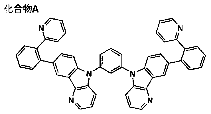
(電子注入層および陰極の形成)
続いて、基板P上に電子注入層、電子輸送層、発光層及び電子輸送層を形成した試料を、大気に曝露することなく真空蒸着装置へ取り付けた。また、モリブデン製抵抗加熱ボートにフッ化ナトリウムおよびフッ化カリウムを入れたものを真空蒸着装置に取り付け、真空槽を4×10⁻⁵Paまで減圧した後、上記モリブデン製抵抗加熱ボートに通電して加熱し、フッ化ナトリウムを0.02nm/秒で電子輸送層上に膜厚1nmの薄膜を形成し、続けて同様にフッ化カリウムを0.02nm/秒でフッ化ナトリウム上に膜厚1.5nmの薄膜を形成した電子注入層を作製した。引き続き、アルミニウム100nmを蒸着して陰極を形成して、有機EL素子102を作製した。
続いて、基板P上に電子注入層、電子輸送層、発光層及び電子輸送層を形成した試料を、大気に曝露することなく真空蒸着装置へ取り付けた。また、モリブデン製抵抗加熱ボートにフッ化ナトリウムおよびフッ化カリウムを入れたものを真空蒸着装置に取り付け、真空槽を4×10⁻⁵Paまで減圧した後、上記モリブデン製抵抗加熱ボートに通電して加熱し、フッ化ナトリウムを0.02nm/秒で電子輸送層上に膜厚1nmの薄膜を形成し、続けて同様にフッ化カリウムを0.02nm/秒でフッ化ナトリウム上に膜厚1.5nmの薄膜を形成した電子注入層を作製した。引き続き、アルミニウム100nmを蒸着して陰極を形成して、有機EL素子102を作製した。
〔有機EL素子103の作製:ロールツーロール方式による有機機能層形成〕
図12に記載のロールツーロール方式による有機機能層の製造ラインに従って、比較例である有機EL素子103を作製した。
図12に記載のロールツーロール方式による有機機能層の製造ラインに従って、比較例である有機EL素子103を作製した。
図12に示すロールツーロール方式による有機機能層の製造ラインは、陽極等を形成した基板積層ロール501を、アンワインダー部より繰り出し、ダンサーロール部506を経て、第1の製膜工程であるStage1に搬送し、塗布工程503で、バックロール505で保持して連続搬送している基板502上に、塗布手段であるダイコータCoを用いて第1の有機機能層、例えば、電子注入層を形成し、乾燥工程504で搬送手段Hを用いて、乾燥させた後、次工程であるStage2にて同様に有機機能層を塗布乾燥して製膜する。Stage3、4を経て有機機能層群を形成した基板502は、ダンサーロール506を経て、ワインダー部で積層ロール507として積層される。
(帯状基体の準備)
厚さ100μm、幅200mm、長さ500mのポリエチレンテレフタレートフィルム(帝人・デュポン社製フィルム、以下、PETと略記する)を準備した。
厚さ100μm、幅200mm、長さ500mのポリエチレンテレフタレートフィルム(帝人・デュポン社製フィルム、以下、PETと略記する)を準備した。
(陽極の形成)
準備したPETに付けられたアライメントマークを検出し、アライメントマークの位置に従って、PETの上に5×10⁻¹Paの真空環境条件で厚さ120nmのITO(インジウムチンオキシド)をスパッタリング法により、マスクパターン成膜を行い、取り出し電極を有する12mm×5mmの大きさの陽極を一定間隔で12列連続的に形成し、一旦巻き取り保管した。
準備したPETに付けられたアライメントマークを検出し、アライメントマークの位置に従って、PETの上に5×10⁻¹Paの真空環境条件で厚さ120nmのITO(インジウムチンオキシド)をスパッタリング法により、マスクパターン成膜を行い、取り出し電極を有する12mm×5mmの大きさの陽極を一定間隔で12列連続的に形成し、一旦巻き取り保管した。
(正孔注入層の形成)
次いで、図12に示すロールツーロール方式による有機機能層の製造ラインに従って、Stage1にて正孔注入層を形成した。
次いで、図12に示すロールツーロール方式による有機機能層の製造ラインに従って、Stage1にて正孔注入層を形成した。
アンワインダー部より、上記陽極まで形成した基板502を繰り出し、Stage1にて、塗布工程303で、図3に示すスリット型ダイコータCoを用い、上記有機EL素子102の作製に用いた正孔注入層塗布液1を、バックロール505で保持された基板502上に、塗布速度5m/min、塗布幅180mm、ウェット膜厚に対するコーターギャップ200μm、正孔注入層形成用塗布液の塗布時の温度は25℃で塗布し、次いで、乾燥工程504で120℃の加熱温風と吹き付けて、厚さ30nmの正孔注入層を形成した。
(正孔輸送層の形成)
次いで、上記と同様にして、Stage2にて、上記有機EL素子102の作製に用いた正孔輸送層塗布液1を用いて、膜厚30nmの正孔輸送層を形成した。
次いで、上記と同様にして、Stage2にて、上記有機EL素子102の作製に用いた正孔輸送層塗布液1を用いて、膜厚30nmの正孔輸送層を形成した。
(発光層の形成)
次いで、上記と同様にして、Stage3にて、上記有機EL素子102の作製に用いた発光層塗布液1を用いて、膜厚40nmの発光層を形成した。
次いで、上記と同様にして、Stage3にて、上記有機EL素子102の作製に用いた発光層塗布液1を用いて、膜厚40nmの発光層を形成した。
(電子輸送層の形成)
次いで、上記と同様にして、Stage4にて、上記有機EL素子102の作製に使用した電子輸送層塗布液1を用い、膜厚30nmの電子輸送層を形成し、アンワインダー部で積層ロール507として巻き取った。
次いで、上記と同様にして、Stage4にて、上記有機EL素子102の作製に使用した電子輸送層塗布液1を用い、膜厚30nmの電子輸送層を形成し、アンワインダー部で積層ロール507として巻き取った。
(電子注入層および陰極の形成)
続いて、基板P上に電子注入層、電子輸送層、発光層及び電子輸送層を形成した試料を所定のサイズに断裁した後、大気に曝露することなく真空蒸着装置へ取り付けた。また、モリブデン製抵抗加熱ボートにフッ化ナトリウムおよびフッ化カリウムを入れたものを真空蒸着装置に取り付け、真空槽を4×10⁻⁵Paまで減圧した後、上記モリブデン製抵抗加熱ボートに通電して加熱し、フッ化ナトリウムを0.02nm/秒で電子輸送層上に膜厚1nmの薄膜を形成し、続けて同様にフッ化カリウムを0.02nm/秒でフッ化ナトリウム上に膜厚1.5nmの薄膜を形成した電子注入層を作製した。引き続き、アルミニウム100nmを蒸着して陰極を形成して、有機EL素子103を作製した。
続いて、基板P上に電子注入層、電子輸送層、発光層及び電子輸送層を形成した試料を所定のサイズに断裁した後、大気に曝露することなく真空蒸着装置へ取り付けた。また、モリブデン製抵抗加熱ボートにフッ化ナトリウムおよびフッ化カリウムを入れたものを真空蒸着装置に取り付け、真空槽を4×10⁻⁵Paまで減圧した後、上記モリブデン製抵抗加熱ボートに通電して加熱し、フッ化ナトリウムを0.02nm/秒で電子輸送層上に膜厚1nmの薄膜を形成し、続けて同様にフッ化カリウムを0.02nm/秒でフッ化ナトリウム上に膜厚1.5nmの薄膜を形成した電子注入層を作製した。引き続き、アルミニウム100nmを蒸着して陰極を形成して、有機EL素子103を作製した。
〔有機EL素子104の作製:インライン方式による有機機能層形成1〕
図2に記載のインライン方式による有機機能層の製造ラインに従って、本発明である有機EL素子104を作製した。
図2に記載のインライン方式による有機機能層の製造ラインに従って、本発明である有機EL素子104を作製した。
(陽極の形成)
150mm×150mm×1.1mmのガラス基板P上に、陽極としてITO(インジウムチンオキシド)を厚さ150nmで製膜した基板(NHテクノグラス製NA45)にパターニングを行った後、このITO透明電極(陽極)を設けた基板P(ITO基板ともいう)をイソプロピルアルコールで超音波洗浄し、乾燥窒素ガスで乾燥し、UVオゾン洗浄を5分間行った。
150mm×150mm×1.1mmのガラス基板P上に、陽極としてITO(インジウムチンオキシド)を厚さ150nmで製膜した基板(NHテクノグラス製NA45)にパターニングを行った後、このITO透明電極(陽極)を設けた基板P(ITO基板ともいう)をイソプロピルアルコールで超音波洗浄し、乾燥窒素ガスで乾燥し、UVオゾン洗浄を5分間行った。
(正孔注入層の形成)
次いで、陽極としてITO透明電極を形成した基板Pを、連続搬送している基板保持ベルト32上に配置し、図2に示すStage1において、図3に示す構成からなるスリット型のダイコータCo1を用い、前記有機EL素子102の作製で使用した正孔注入層塗布液1を用い、塗布速度3m/min、正孔注入層形成用塗布液の塗布時の温度を25℃に設定し、乾燥後の正孔注入層L1の膜厚が30nmとなる条件で塗布し、次いで、下流に配置されている乾燥部H1で120℃の加熱温風を吹き付けて、正孔注入層L1を形成した。
次いで、陽極としてITO透明電極を形成した基板Pを、連続搬送している基板保持ベルト32上に配置し、図2に示すStage1において、図3に示す構成からなるスリット型のダイコータCo1を用い、前記有機EL素子102の作製で使用した正孔注入層塗布液1を用い、塗布速度3m/min、正孔注入層形成用塗布液の塗布時の温度を25℃に設定し、乾燥後の正孔注入層L1の膜厚が30nmとなる条件で塗布し、次いで、下流に配置されている乾燥部H1で120℃の加熱温風を吹き付けて、正孔注入層L1を形成した。
なお、第1の製膜環境30(エリア1)における正孔注入層L1の形成は、不活性ガスとして窒素ガスを用い、酸素濃度300ppm、水分濃度300ppmの雰囲気下31で行った。
(正孔輸送層の形成)
次いで、正孔注入層L1を形成した基板Pを、図2に示すStage2に移送し、図3に示す構成からなるスリット型のダイコータCo2を用い、前記有機EL素子102の作製で使用した正孔輸送層塗布液1を用い、塗布速度3m/min、正孔輸送層形成用塗布液の塗布時の温度を25℃に設定し、乾燥後の正孔輸送層L2の膜厚が30nmとなる条件で塗布し、次いで、下流に配置されている乾燥部H2で120℃の加熱温風を吹き付けて、正孔輸送層L2を形成した。
次いで、正孔注入層L1を形成した基板Pを、図2に示すStage2に移送し、図3に示す構成からなるスリット型のダイコータCo2を用い、前記有機EL素子102の作製で使用した正孔輸送層塗布液1を用い、塗布速度3m/min、正孔輸送層形成用塗布液の塗布時の温度を25℃に設定し、乾燥後の正孔輸送層L2の膜厚が30nmとなる条件で塗布し、次いで、下流に配置されている乾燥部H2で120℃の加熱温風を吹き付けて、正孔輸送層L2を形成した。
なお、第1の製膜環境30(エリア1)における正孔輸送層L2の形成は、不活性ガスとして窒素ガスを用い、酸素濃度300ppm、水分濃度300ppmの雰囲気下31で行った。
(発光層の形成)
次いで、正孔輸送層L2を形成した基板Pを、図2に示すStage3に移送し、図3に示す構成からなるスリット型のダイコータCo3を用い、前記有機EL素子102の作製で使用した発光層塗布液1を用い、塗布速度3m/min、発光層形成用塗布液の塗布時の温度を25℃に設定し、乾燥後の発光層L3の膜厚が30nmとなる条件で塗布し、次いで、下流に配置されている乾燥部H3で120℃の加熱温風を吹き付けて、発光層L3を形成した。
次いで、正孔輸送層L2を形成した基板Pを、図2に示すStage3に移送し、図3に示す構成からなるスリット型のダイコータCo3を用い、前記有機EL素子102の作製で使用した発光層塗布液1を用い、塗布速度3m/min、発光層形成用塗布液の塗布時の温度を25℃に設定し、乾燥後の発光層L3の膜厚が30nmとなる条件で塗布し、次いで、下流に配置されている乾燥部H3で120℃の加熱温風を吹き付けて、発光層L3を形成した。
なお、第1の製膜環境30(エリア1)における発光層L3の形成は、不活性ガスとして窒素ガスを用い、酸素濃度300ppm、水分濃度300ppmの雰囲気下31で行った。
(電子輸送層の形成)
次いで、発光層L3を形成した基板Pを、図2に示すStage4に移送し、図3に示す構成からなるスリット型のダイコータCo4を用い、前記有機EL素子102の作製で使用した電子輸送層塗布液1を用い、塗布速度3m/min、電子輸送層形成用塗布液の塗布時の温度を25℃に設定し、乾燥後の電子輸送層L4の膜厚が30nmとなる条件で塗布し、次いで、下流に配置されている乾燥部H4で120℃の加熱温風を吹き付けて、電子輸送層L4を形成した。
次いで、発光層L3を形成した基板Pを、図2に示すStage4に移送し、図3に示す構成からなるスリット型のダイコータCo4を用い、前記有機EL素子102の作製で使用した電子輸送層塗布液1を用い、塗布速度3m/min、電子輸送層形成用塗布液の塗布時の温度を25℃に設定し、乾燥後の電子輸送層L4の膜厚が30nmとなる条件で塗布し、次いで、下流に配置されている乾燥部H4で120℃の加熱温風を吹き付けて、電子輸送層L4を形成した。
なお、第1の製膜環境30(エリア1)における電子輸送層L4の形成は、不活性ガスとして窒素ガスを用い、酸素濃度300ppm、水分濃度300ppmの雰囲気下31で行った。
(ベーク処理工程)
続いて、基板P上に電子注入層、電子輸送層、発光層及び電子輸送層を形成した試料を連続搬送している基板保持ベルト32より取り外し、第2の製膜環境40に移動し、加熱部H5より120℃の加熱温風を60分間吹き付けて、ベーク処理を施した。
続いて、基板P上に電子注入層、電子輸送層、発光層及び電子輸送層を形成した試料を連続搬送している基板保持ベルト32より取り外し、第2の製膜環境40に移動し、加熱部H5より120℃の加熱温風を60分間吹き付けて、ベーク処理を施した。
ベーク処理時の第2の製膜環境40(エリア2)としては、不活性ガスとして窒素ガスを用い、酸素濃度90ppm、水分濃度90ppmの雰囲気下41で行った。
(電子注入層および陰極の形成)
続いて、ベーク処理を施した電子注入層、電子輸送層、発光層及び電子輸送層まで形成した基板Pを、大気に曝露することなく真空蒸着装置へ取り付けた。
続いて、ベーク処理を施した電子注入層、電子輸送層、発光層及び電子輸送層まで形成した基板Pを、大気に曝露することなく真空蒸着装置へ取り付けた。
真空蒸着装置内のモリブデン製抵抗加熱ボートにフッ化ナトリウムおよびフッ化カリウムを入れたものを真空蒸着装置に取り付け、真空槽を4×10⁻⁵Paまで減圧した後、上記モリブデン製抵抗加熱ボートに通電して加熱し、フッ化ナトリウムを0.02nm/秒で電子輸送層上に膜厚1nmの薄膜を形成し、続けて同様にフッ化カリウムを0.02nm/秒でフッ化ナトリウム上に膜厚1.5nmの薄膜を形成し電子注入層を得た。引き続き、アルミニウム100nmを蒸着して陰極を形成して、有機EL素子104を作製した。
〔有機EL素子105の作製:インライン方式による有機機能層形成2〕
上記有機EL素子104の作製において、Stage1~4において、乾燥部H1~H4による乾燥は行わずに、ベーク処理工程でのみ、加熱部H5より120℃の加熱温風を60分間吹き付けて、ベーク処理(乾燥処理)を施した以外は同様にして、有機EL素子105を作製した。
上記有機EL素子104の作製において、Stage1~4において、乾燥部H1~H4による乾燥は行わずに、ベーク処理工程でのみ、加熱部H5より120℃の加熱温風を60分間吹き付けて、ベーク処理(乾燥処理)を施した以外は同様にして、有機EL素子105を作製した。
《有機EL素子の生産適性の評価》
〔生産効率の評価〕
有機EL素子104の作製方法において、有機EL素子を1枚作製に要する時間を1.00として、各有機EL素子を作製するのに要する相対時間を算出し、下記の基準に従って生産効率を評価した。
〔生産効率の評価〕
有機EL素子104の作製方法において、有機EL素子を1枚作製に要する時間を1.00として、各有機EL素子を作製するのに要する相対時間を算出し、下記の基準に従って生産効率を評価した。
◎:有機EL素子1枚を作製するのに要する相対時間が、0.90未満である
○:有機EL素子1枚を作製するのに要する相対時間が、0.90以上、1.10未満である
△:有機EL素子1枚を作製するのに要する相対時間が、1.10以上、1.50未満である
×:有機EL素子1枚を作製するのに要する相対時間が、1.50以上である
〔設備投資コストの評価〕
有機EL素子104の作製に適用する設備費用を1.00として、各有機EL素子を作製に適用する設備費用を算出し、下記の基準に従って設備投資コストを評価した。
○:有機EL素子1枚を作製するのに要する相対時間が、0.90以上、1.10未満である
△:有機EL素子1枚を作製するのに要する相対時間が、1.10以上、1.50未満である
×:有機EL素子1枚を作製するのに要する相対時間が、1.50以上である
〔設備投資コストの評価〕
有機EL素子104の作製に適用する設備費用を1.00として、各有機EL素子を作製に適用する設備費用を算出し、下記の基準に従って設備投資コストを評価した。
◎:有機EL素子の作製に適用する製造設備の相対投資費用が、0.90未満である
○:有機EL素子の作製に適用する製造設備の相対投資費用が、0.90以上、1.10未満である
△:有機EL素子の作製に適用する製造設備の相対投資費用が、1.10以上、1.50未満である
×:有機EL素子の作製に適用する製造設備の相対投資費用が、1.50以上である
《有機EL素子の品質評価》
〔量子効率の測定〕
各有機EL素子について、分光放射輝度計CS-1000(コニカミノルタセンシング社製)を用い、23℃、乾燥窒素ガス雰囲気下で2.5mA/cm2定電流を印加した時の外部取り出し量子効率(%)を測定した。量子効率は、有機EL素子104の量子効率を100とした相対値で表示した。数値が大きいほど、外部取り出し量子効率に優れていることを表す。
○:有機EL素子の作製に適用する製造設備の相対投資費用が、0.90以上、1.10未満である
△:有機EL素子の作製に適用する製造設備の相対投資費用が、1.10以上、1.50未満である
×:有機EL素子の作製に適用する製造設備の相対投資費用が、1.50以上である
《有機EL素子の品質評価》
〔量子効率の測定〕
各有機EL素子について、分光放射輝度計CS-1000(コニカミノルタセンシング社製)を用い、23℃、乾燥窒素ガス雰囲気下で2.5mA/cm2定電流を印加した時の外部取り出し量子効率(%)を測定した。量子効率は、有機EL素子104の量子効率を100とした相対値で表示した。数値が大きいほど、外部取り出し量子効率に優れていることを表す。
〔発光寿命の測定〕
作製した各有機EL素子に対し、正面輝度1000cd/m2となるような電流を与え、連続駆動した。正面輝度が初期の半減値(500cd/m2)になるまでに要する時間(発光寿命)を求めた。測定には分光放射輝度計CS-1000(コニカミノルタセンシング社製)を用い、有機EL素子104の発光寿命を100とした相対値で表示した。数値が大きいほど、発光寿命に優れていることを表す。
作製した各有機EL素子に対し、正面輝度1000cd/m2となるような電流を与え、連続駆動した。正面輝度が初期の半減値(500cd/m2)になるまでに要する時間(発光寿命)を求めた。測定には分光放射輝度計CS-1000(コニカミノルタセンシング社製)を用い、有機EL素子104の発光寿命を100とした相対値で表示した。数値が大きいほど、発光寿命に優れていることを表す。
〔輝度ムラ耐性の評価〕
作製した各有機EL素子に対し、2.5mA/cm2の定電流を印加したときの発光面内輝度分布を、Prometric(サイバネットシステム社製)で測定した。なお、輝度分布は、発光面を均等に40分割したときの各発光面内輝度の標準偏差として表した。数値が低いほど、輝度ムラが少なく、輝度ムラ耐性に優れていることを表す。
作製した各有機EL素子に対し、2.5mA/cm2の定電流を印加したときの発光面内輝度分布を、Prometric(サイバネットシステム社製)で測定した。なお、輝度分布は、発光面を均等に40分割したときの各発光面内輝度の標準偏差として表した。数値が低いほど、輝度ムラが少なく、輝度ムラ耐性に優れていることを表す。
以上により得られた結果を、表1に示す。
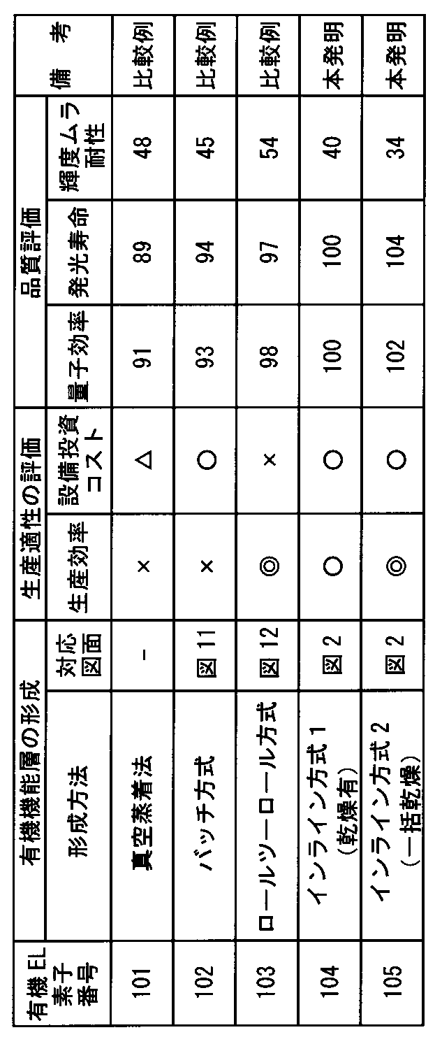
表1に記載の結果より明らかなように、本発明で規定する有機EL素子の製造方法は、従来の製造方法に対し、生産効率と設備投資コストとの両立が図られ、かつ製造される有機EL素子の量子効率、発光寿命及び輝度ムラ耐性に優れていることが分かる。
実施例2
《有機EL素子201~203の作製》
実施例1に記載の有機EL素子104(第1の製膜環境30(エリア1)における塗布速度:3m/min)において、第1の製膜環境30(エリア1)における塗布速度を、それぞれ5m/min、10m/min、15m/minに変更した以外は同様にして、有機EL素子201~203を作製した。
《有機EL素子201~203の作製》
実施例1に記載の有機EL素子104(第1の製膜環境30(エリア1)における塗布速度:3m/min)において、第1の製膜環境30(エリア1)における塗布速度を、それぞれ5m/min、10m/min、15m/minに変更した以外は同様にして、有機EL素子201~203を作製した。
《有機EL素子の生産適性、品質評価》
上記作製した有機EL素子201~203と実施例1で作製した有機EL素子104について、実施例1に記載の方法と同様にして、生産効率、量子効率、発光寿命及び輝度ムラ耐性の評価を行い、得られた結果を表2に示す。
上記作製した有機EL素子201~203と実施例1で作製した有機EL素子104について、実施例1に記載の方法と同様にして、生産効率、量子効率、発光寿命及び輝度ムラ耐性の評価を行い、得られた結果を表2に示す。
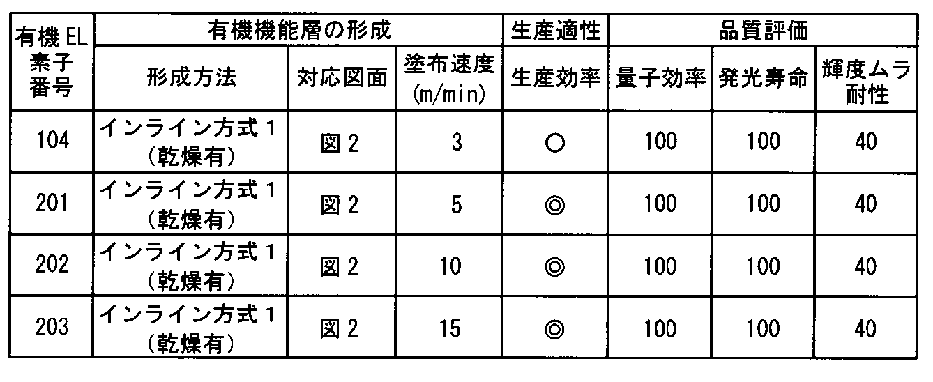
有機EL素子の製造における第1の製膜環境30(エリア1)の塗布速度を5m/min以上とすることで、量子効率、発光寿命及び輝度ムラ耐性等の特性を損なうことなく、生産効率を高めることができる。
実施例3
《有機EL素子301~309の作製》
実施例1に記載の有機EL素子105(第1の製膜環境(エリア1):不活性ガスとして窒素ガスを用い、酸素濃度300ppm、水分濃度300ppmの雰囲気下。第2の製膜環境(エリア2):不活性ガスとして窒素ガスを用い、酸素濃度90ppm、水分濃度90ppmの雰囲気下)において、第1の製膜環境(エリア1)における雰囲気組成及び第2の製膜環境(エリア2)における雰囲気組成を、表3に記載の条件にそれぞれ変更した以外は同様にして、有機EL素子301~309を作製した。
《有機EL素子301~309の作製》
実施例1に記載の有機EL素子105(第1の製膜環境(エリア1):不活性ガスとして窒素ガスを用い、酸素濃度300ppm、水分濃度300ppmの雰囲気下。第2の製膜環境(エリア2):不活性ガスとして窒素ガスを用い、酸素濃度90ppm、水分濃度90ppmの雰囲気下)において、第1の製膜環境(エリア1)における雰囲気組成及び第2の製膜環境(エリア2)における雰囲気組成を、表3に記載の条件にそれぞれ変更した以外は同様にして、有機EL素子301~309を作製した。
《有機EL素子の品質評価》
上記作製した有機EL素子301~309と実施例1で作製した有機EL素子105について、下記の方法により生産コストの評価と、実施例1に記載の方法と同様にして、量子効率、発光寿命及び輝度ムラ耐性の評価を行い、得られた結果を表3に示す。
上記作製した有機EL素子301~309と実施例1で作製した有機EL素子105について、下記の方法により生産コストの評価と、実施例1に記載の方法と同様にして、量子効率、発光寿命及び輝度ムラ耐性の評価を行い、得られた結果を表3に示す。
〔生産コスト〕
有機EL素子105の作製において、有機機能層形成に要するコストを1.00とし、下記の基準に従って、相対生産コストの評価を行った。
有機EL素子105の作製において、有機機能層形成に要するコストを1.00とし、下記の基準に従って、相対生産コストの評価を行った。
◎:有機EL素子の相対生産コストが、1.05以上である
○:有機EL素子の相対生産コストが、0.95以上、1.05未満である
△:有機EL素子の相対生産コストが、0.90以上、0.95未満である
×:有機EL素子の相対生産コストが、0.90未満である
○:有機EL素子の相対生産コストが、0.95以上、1.05未満である
△:有機EL素子の相対生産コストが、0.90以上、0.95未満である
×:有機EL素子の相対生産コストが、0.90未満である

本発明の有機ELの製造方法において、第1の製膜環境(エリア1)における不活性ガス以外のガス成分濃度を500ppm以上とし、かつ第2の製膜環境(エリア2)における不活性ガス以外のガス成分濃度を200ppm以下とすることにより、生産コストに優れ、量子効率、発光寿命及び輝度ムラ耐性がより向上していることが分かる。
実施例4
《有機EL素子401~408の作製》
実施例1に記載の有機EL素子105(ガラス基板、第2の製膜環境(エリア2)におけるベーク条件:120℃、60分)において、基板の種類(樹脂基板:厚さ100μmのポリエチレンテレフタレートフィルム、ガラス基板:厚さ1.1mmのNHテクノグラス製、NA45)及び第2の製膜環境(エリア2)におけるベーク条件を、表4に記載の条件にそれぞれ変更した以外は同様にして、有機EL素子401~408を作製した。
《有機EL素子401~408の作製》
実施例1に記載の有機EL素子105(ガラス基板、第2の製膜環境(エリア2)におけるベーク条件:120℃、60分)において、基板の種類(樹脂基板:厚さ100μmのポリエチレンテレフタレートフィルム、ガラス基板:厚さ1.1mmのNHテクノグラス製、NA45)及び第2の製膜環境(エリア2)におけるベーク条件を、表4に記載の条件にそれぞれ変更した以外は同様にして、有機EL素子401~408を作製した。
《有機EL素子の品質評価》
上記作製した有機EL素子401~408と実施例1で作製した有機EL素子105について、実施例1に記載の方法と同様にして、生産効率、量子効率、発光寿命及び輝度ムラ耐性の評価を行い、得られた結果を表4に示す。
上記作製した有機EL素子401~408と実施例1で作製した有機EL素子105について、実施例1に記載の方法と同様にして、生産効率、量子効率、発光寿命及び輝度ムラ耐性の評価を行い、得られた結果を表4に示す。
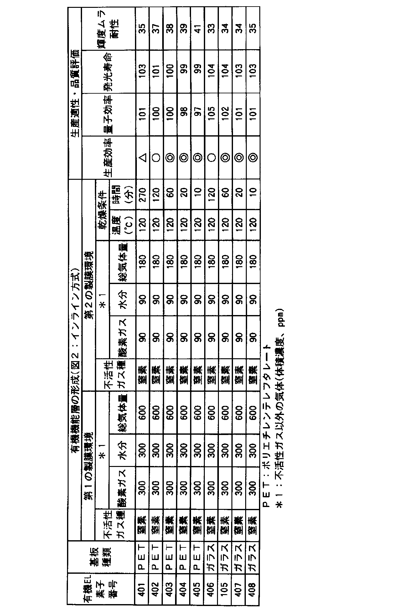
本発明の有機ELの製造方法において、基板としてガラス基板を用いることにより、樹脂基板を用いた有機EL素子に比較して、生産効率が高く、第2の製膜環境(エリア2)におけるベーク時間を短くしても、性能低下が小さいことが分かる。これは、ガラス基板は、有機機能層を塗布した際に、樹脂基板に比較して、基板中への各塗布液を構成する溶剤等の侵入が少なく、その結果、短時間であっても所望の特性を得ることができたと推測している。
実施例5
〔有機EL素子502の作製〕
図4に記載のインライン方式による有機機能層の製造ラインにおいて、基板浮上部55による基板の浮上は行わずに、基板保持部材上に直接配置して塗布を行って、有機EL素子502を作製した。
〔有機EL素子502の作製〕
図4に記載のインライン方式による有機機能層の製造ラインにおいて、基板浮上部55による基板の浮上は行わずに、基板保持部材上に直接配置して塗布を行って、有機EL素子502を作製した。
(アライメントマークの付与)
150mm×150mm×1.1mmのガラス基板Pの4隅に、アライメントマークを付与した。
150mm×150mm×1.1mmのガラス基板Pの4隅に、アライメントマークを付与した。
アライメントマークの付与は、5×10⁻¹Paの真空環境条件でガラス基板P上の4隅に、厚さ120nmのITO(インジウムチンオキシド)膜による十字マークをスパッタリング法により形成した。
(陽極の形成)
150mm×150mm×1.1mmのガラス基板P上に、陽極としてITO(インジウムチンオキシド)を厚さ150nmで製膜した基板(NHテクノグラス製NA45)にパターニングを行った後、このITO透明電極(陽極)を設けた基板P(ITO基板ともいう)をイソプロピルアルコールで超音波洗浄し、乾燥窒素ガスで乾燥し、UVオゾン洗浄を5分間行った。
150mm×150mm×1.1mmのガラス基板P上に、陽極としてITO(インジウムチンオキシド)を厚さ150nmで製膜した基板(NHテクノグラス製NA45)にパターニングを行った後、このITO透明電極(陽極)を設けた基板P(ITO基板ともいう)をイソプロピルアルコールで超音波洗浄し、乾燥窒素ガスで乾燥し、UVオゾン洗浄を5分間行った。
(正孔注入層の形成)
次いで、陽極としてITO透明電極を形成した基板Pを、連続搬送している基板保持部材32上に配置し、図4に示すStage1において、図6に示す構成からなるスリット型のダイコータCo1を用い、アライメントマークをCCDカメラで検知し、その情報に従って、基板P上に前記有機EL素子102の作製で使用した正孔注入層塗布液1を、基板を全く浮上させないで、塗布速度3m/min、正孔注入層形成用塗布液の塗布時の温度を25℃に設定し、乾燥後の正孔注入層L1の膜厚が30nmとなる条件で塗布し、次いで、下流に配置されている乾燥部H1で120℃の加熱温風を吹き付けて、正孔注入層L1を形成した。
次いで、陽極としてITO透明電極を形成した基板Pを、連続搬送している基板保持部材32上に配置し、図4に示すStage1において、図6に示す構成からなるスリット型のダイコータCo1を用い、アライメントマークをCCDカメラで検知し、その情報に従って、基板P上に前記有機EL素子102の作製で使用した正孔注入層塗布液1を、基板を全く浮上させないで、塗布速度3m/min、正孔注入層形成用塗布液の塗布時の温度を25℃に設定し、乾燥後の正孔注入層L1の膜厚が30nmとなる条件で塗布し、次いで、下流に配置されている乾燥部H1で120℃の加熱温風を吹き付けて、正孔注入層L1を形成した。
なお、第1の製膜環境30(エリア1)における正孔注入層L1の形成は、不活性ガスとして窒素ガスを用い、酸素濃度300ppm、水分濃度300ppmの雰囲気下31で行った。
(正孔輸送層の形成)
次いで、正孔注入層L1を形成した基板Pを、図4に示すStage2に移送し、図6に示す構成からなるスリット型のダイコータCo2を用い、前記有機EL素子102の作製で使用した正孔輸送層塗布液1を用い、アライメントマークのCCDカメラによる検知情報に従って、基板を全く浮上させないで、塗布速度3m/min、正孔輸送層形成用塗布液の塗布時の温度を25℃に設定し、乾燥後の正孔輸送層L2の膜厚が30nmとなる条件で塗布し、次いで、下流に配置されている乾燥部H2で120℃の加熱温風を吹き付けて、正孔輸送層L2を形成した。
次いで、正孔注入層L1を形成した基板Pを、図4に示すStage2に移送し、図6に示す構成からなるスリット型のダイコータCo2を用い、前記有機EL素子102の作製で使用した正孔輸送層塗布液1を用い、アライメントマークのCCDカメラによる検知情報に従って、基板を全く浮上させないで、塗布速度3m/min、正孔輸送層形成用塗布液の塗布時の温度を25℃に設定し、乾燥後の正孔輸送層L2の膜厚が30nmとなる条件で塗布し、次いで、下流に配置されている乾燥部H2で120℃の加熱温風を吹き付けて、正孔輸送層L2を形成した。
なお、第1の製膜環境30(エリア1)における正孔輸送層L2の形成は、不活性ガスとして窒素ガスを用い、酸素濃度300ppm、水分濃度300ppmの雰囲気下31で行った。
(発光層の形成)
次いで、正孔輸送層L2を形成した基板Pを、図4に示すStage3に移送し、図6に示す構成からなるスリット型のダイコータCo3を用い、前記有機EL素子102の作製で使用した発光層塗布液1を用い、CCDカメラによるアライメントマークの検知情報に従って、基板を全く浮上させないで、基板を全く浮上させないで、塗布速度3m/min、発光層形成用塗布液の塗布時の温度を25℃に設定し、乾燥後の発光層L3の膜厚が30nmとなる条件で塗布し、次いで、下流に配置されている乾燥部H3で120℃の加熱温風を吹き付けて、発光層L3を形成した。
次いで、正孔輸送層L2を形成した基板Pを、図4に示すStage3に移送し、図6に示す構成からなるスリット型のダイコータCo3を用い、前記有機EL素子102の作製で使用した発光層塗布液1を用い、CCDカメラによるアライメントマークの検知情報に従って、基板を全く浮上させないで、基板を全く浮上させないで、塗布速度3m/min、発光層形成用塗布液の塗布時の温度を25℃に設定し、乾燥後の発光層L3の膜厚が30nmとなる条件で塗布し、次いで、下流に配置されている乾燥部H3で120℃の加熱温風を吹き付けて、発光層L3を形成した。
なお、第1の製膜環境30(エリア1)における発光層L3の形成は、不活性ガスとして窒素ガスを用い、酸素濃度300ppm、水分濃度300ppmの雰囲気下31で行った。
(電子輸送層の形成)
次いで、発光層L3を形成した基板Pを、図4に示すStage4に移送し、図6に示す構成からなるスリット型のダイコータCo4を用い、前記有機EL素子102の作製で使用した電子輸送層塗布液1を用い、CCDカメラによるアライメントマークの検知情報に従って、基板を全く浮上させないで、塗布速度3m/min、電子輸送層形成用塗布液の塗布時の温度を25℃に設定し、乾燥後の電子輸送層L4の膜厚が30nmとなる条件で塗布し、次いで、下流に配置されている乾燥部H4で120℃の加熱温風を吹き付けて、電子輸送層L4を形成した。
次いで、発光層L3を形成した基板Pを、図4に示すStage4に移送し、図6に示す構成からなるスリット型のダイコータCo4を用い、前記有機EL素子102の作製で使用した電子輸送層塗布液1を用い、CCDカメラによるアライメントマークの検知情報に従って、基板を全く浮上させないで、塗布速度3m/min、電子輸送層形成用塗布液の塗布時の温度を25℃に設定し、乾燥後の電子輸送層L4の膜厚が30nmとなる条件で塗布し、次いで、下流に配置されている乾燥部H4で120℃の加熱温風を吹き付けて、電子輸送層L4を形成した。
なお、第1の製膜環境30(エリア1)における電子輸送層L4の形成は、不活性ガスとして窒素ガスを用い、酸素濃度300ppm、水分濃度300ppmの雰囲気下31で行った。
(ベーク処理工程)
続いて、基板P上に電子注入層、電子輸送層、発光層及び電子輸送層を形成した試料を連続搬送している基板保持部材32より取り外し、第2の製膜環境40に移動し、加熱部H5より120℃の加熱温風を60分間吹き付けて、ベーク処理を施した。
続いて、基板P上に電子注入層、電子輸送層、発光層及び電子輸送層を形成した試料を連続搬送している基板保持部材32より取り外し、第2の製膜環境40に移動し、加熱部H5より120℃の加熱温風を60分間吹き付けて、ベーク処理を施した。
ベーク処理時の第2の製膜環境40(エリア2)としては、不活性ガスとして窒素ガスを用い、酸素濃度90ppm、水分濃度90ppmの雰囲気下41で行った。
(電子注入層および陰極の形成)
続いて、ベーク処理を施した電子注入層、電子輸送層、発光層及び電子輸送層まで形成した基板Pを、大気に曝露することなく真空蒸着装置へ取り付けた。
続いて、ベーク処理を施した電子注入層、電子輸送層、発光層及び電子輸送層まで形成した基板Pを、大気に曝露することなく真空蒸着装置へ取り付けた。
真空蒸着装置内のモリブデン製抵抗加熱ボートにフッ化ナトリウムおよびフッ化カリウムを入れたものを真空蒸着装置に取り付け、真空槽を4×10⁻⁵Paまで減圧した後、上記モリブデン製抵抗加熱ボートに通電して加熱し、フッ化ナトリウムを0.02nm/秒で電子輸送層上に膜厚1nmの薄膜を形成し、続けて同様にフッ化カリウムを0.02nm/秒でフッ化ナトリウム上に膜厚1.5nmの薄膜を形成し電子注入層を得た。引き続き、アルミニウム100nmを蒸着して陰極を形成して、有機EL素子502を作製した。
〔有機EL素子503の作製:基板浮上方式〕
図4に記載のインライン方式による有機機能層の製造ラインを用い、図7に示す構造からなる基板浮上部により、基板を浮上させながら塗布を行って、有機EL素子503を作製した。
図4に記載のインライン方式による有機機能層の製造ラインを用い、図7に示す構造からなる基板浮上部により、基板を浮上させながら塗布を行って、有機EL素子503を作製した。
(アライメントマークの付与)
150mm×150mm×1.1mmのガラス基板Pの4隅に、アライメントマークを付与した。
150mm×150mm×1.1mmのガラス基板Pの4隅に、アライメントマークを付与した。
アライメントマークの付与は、5×10⁻¹Paの真空環境条件でガラス基板P上の4隅に、厚さ120nmのITO(インジウムチンオキシド)膜による十字マークをスパッタリング法により形成した。
(陽極の形成)
150mm×150mm×1.1mmのガラス基板P上に、陽極としてITO(インジウムチンオキシド)を厚さ150nmで製膜した基板(NHテクノグラス製NA45)にパターニングを行った後、このITO透明電極(陽極)を設けた基板P(ITO基板ともいう)をイソプロピルアルコールで超音波洗浄し、乾燥窒素ガスで乾燥し、UVオゾン洗浄を5分間行った。
150mm×150mm×1.1mmのガラス基板P上に、陽極としてITO(インジウムチンオキシド)を厚さ150nmで製膜した基板(NHテクノグラス製NA45)にパターニングを行った後、このITO透明電極(陽極)を設けた基板P(ITO基板ともいう)をイソプロピルアルコールで超音波洗浄し、乾燥窒素ガスで乾燥し、UVオゾン洗浄を5分間行った。
(正孔注入層の形成)
次いで、陽極としてITO透明電極を形成した基板Pを、連続搬送している基板保持部材32上に配置し、図4に示すStage1において、図6に示す構成からなるスリット型のダイコータCo1を用い、アライメントマークをCCDカメラにより検知し、得られた基板の位置情報に従って、図7で示す基板浮上部により、基板Pを浮上させた。浮上方法は、2基に圧縮気体供給部300A、300Bに、不活性ガスが窒素ガスで、酸素濃度が300ppm、水分濃度が300ppmの圧縮気体を、気体送風ポンプ304A、304Bで供給した。一方、真空ポンプ305を稼働させて減圧部306より吸気を行った。
次いで、陽極としてITO透明電極を形成した基板Pを、連続搬送している基板保持部材32上に配置し、図4に示すStage1において、図6に示す構成からなるスリット型のダイコータCo1を用い、アライメントマークをCCDカメラにより検知し、得られた基板の位置情報に従って、図7で示す基板浮上部により、基板Pを浮上させた。浮上方法は、2基に圧縮気体供給部300A、300Bに、不活性ガスが窒素ガスで、酸素濃度が300ppm、水分濃度が300ppmの圧縮気体を、気体送風ポンプ304A、304Bで供給した。一方、真空ポンプ305を稼働させて減圧部306より吸気を行った。
次いで、位置検知センサー307により、基板保持部材32に対する基板Pの浮上量H1を150μmに制御し、塗布コータCoの先端のリップと基板P表面との高さH2(ビードギャップ)が300μmとなるように、圧縮気体の送風量と、減圧部306より吸気量を制御した。
上記条件で、基板P上に前記有機EL素子102の作製で使用した正孔注入層塗布液1を、塗布速度3m/min、正孔注入層形成用塗布液の塗布時の温度を25℃に設定し、乾燥後の正孔注入層L1の膜厚が30nmとなる条件で塗布し、次いで、下流に配置されている乾燥部H1で120℃の加熱温風を吹き付けて、正孔注入層L1を形成した。
なお、第1の製膜環境30(エリア1)における正孔注入層L1の形成は、不活性ガスとして窒素ガスを用い、酸素濃度300ppm、水分濃度300ppmの雰囲気下31で行った。
(正孔輸送層の形成)
次いで、正孔注入層L1を形成した基板Pを、図4に示すStage2に移送し、図6に示す構成からなるスリット型のダイコータCo2を用い、前記有機EL素子102の作製で使用した正孔輸送層塗布液1を用い、上記正孔注入層の浮上条件と同様にして、基板を150μmの高さで浮上させながら、塗布速度3m/min、正孔輸送層形成用塗布液の塗布時の温度を25℃に設定し、乾燥後の正孔輸送層L2の膜厚が30nmとなる条件で塗布し、次いで、下流に配置されている乾燥部H2で120℃の加熱温風を吹き付けて、正孔輸送層L2を形成した。
次いで、正孔注入層L1を形成した基板Pを、図4に示すStage2に移送し、図6に示す構成からなるスリット型のダイコータCo2を用い、前記有機EL素子102の作製で使用した正孔輸送層塗布液1を用い、上記正孔注入層の浮上条件と同様にして、基板を150μmの高さで浮上させながら、塗布速度3m/min、正孔輸送層形成用塗布液の塗布時の温度を25℃に設定し、乾燥後の正孔輸送層L2の膜厚が30nmとなる条件で塗布し、次いで、下流に配置されている乾燥部H2で120℃の加熱温風を吹き付けて、正孔輸送層L2を形成した。
なお、第1の製膜環境30(エリア1)における正孔輸送層L2の形成は、不活性ガスとして窒素ガスを用い、酸素濃度300ppm、水分濃度300ppmの雰囲気下31で行った。
(発光層の形成)
次いで、正孔輸送層L2を形成した基板Pを、図4に示すStage3に移送し、図6に示す構成からなるスリット型のダイコータCo3を用い、前記有機EL素子102の作製で使用した発光層塗布液1を用い、上記正孔注入層の浮上条件と同様にして、基板を150μmの高さで浮上させながら、塗布速度3m/min、発光層形成用塗布液の塗布時の温度を25℃に設定し、乾燥後の発光層L3の膜厚が30nmとなる条件で塗布し、次いで、下流に配置されている乾燥部H3で120℃の加熱温風を吹き付けて、発光層L3を形成した。
次いで、正孔輸送層L2を形成した基板Pを、図4に示すStage3に移送し、図6に示す構成からなるスリット型のダイコータCo3を用い、前記有機EL素子102の作製で使用した発光層塗布液1を用い、上記正孔注入層の浮上条件と同様にして、基板を150μmの高さで浮上させながら、塗布速度3m/min、発光層形成用塗布液の塗布時の温度を25℃に設定し、乾燥後の発光層L3の膜厚が30nmとなる条件で塗布し、次いで、下流に配置されている乾燥部H3で120℃の加熱温風を吹き付けて、発光層L3を形成した。
なお、第1の製膜環境30(エリア1)における発光層L3の形成は、不活性ガスとして窒素ガスを用い、酸素濃度300ppm、水分濃度300ppmの雰囲気下31で行った。
(電子輸送層の形成)
次いで、発光層L3を形成した基板Pを、図4に示すStage4に移送し、図6に示す構成からなるスリット型のダイコータCo4を用い、前記有機EL素子102の作製で使用した電子輸送層塗布液1を用い、上記正孔注入層の浮上条件と同様にして、基板を150μmの高さで浮上させながら、塗布速度3m/min、電子輸送層形成用塗布液の塗布時の温度を25℃に設定し、乾燥後の電子輸送層L4の膜厚が30nmとなる条件で塗布し、次いで、下流に配置されている乾燥部H4で120℃の加熱温風を吹き付けて、電子輸送層L4を形成した。
次いで、発光層L3を形成した基板Pを、図4に示すStage4に移送し、図6に示す構成からなるスリット型のダイコータCo4を用い、前記有機EL素子102の作製で使用した電子輸送層塗布液1を用い、上記正孔注入層の浮上条件と同様にして、基板を150μmの高さで浮上させながら、塗布速度3m/min、電子輸送層形成用塗布液の塗布時の温度を25℃に設定し、乾燥後の電子輸送層L4の膜厚が30nmとなる条件で塗布し、次いで、下流に配置されている乾燥部H4で120℃の加熱温風を吹き付けて、電子輸送層L4を形成した。
なお、第1の製膜環境30(エリア1)における電子輸送層L4の形成は、不活性ガスとして窒素ガスを用い、酸素濃度300ppm、水分濃度300ppmの雰囲気下31で行った。
(ベーク処理工程)
続いて、基板P上に電子注入層、電子輸送層、発光層及び電子輸送層を形成した試料を連続搬送している基板保持部材32より取り外し、第2の製膜環境40に移動し、加熱部H5より120℃の加熱温風を60分間吹き付けて、ベーク処理を施した。
続いて、基板P上に電子注入層、電子輸送層、発光層及び電子輸送層を形成した試料を連続搬送している基板保持部材32より取り外し、第2の製膜環境40に移動し、加熱部H5より120℃の加熱温風を60分間吹き付けて、ベーク処理を施した。
ベーク処理時の第2の製膜環境40(エリア2)としては、不活性ガスとして窒素ガスを用い、酸素濃度90ppm、水分濃度90ppmの雰囲気下41で行った。
(電子注入層および陰極の形成)
続いて、ベーク処理を施した電子注入層、電子輸送層、発光層及び電子輸送層まで形成した基板Pを、大気に曝露することなく真空蒸着装置へ取り付けた。
続いて、ベーク処理を施した電子注入層、電子輸送層、発光層及び電子輸送層まで形成した基板Pを、大気に曝露することなく真空蒸着装置へ取り付けた。
真空蒸着装置内のモリブデン製抵抗加熱ボートにフッ化ナトリウムおよびフッ化カリウムを入れたものを真空蒸着装置に取り付け、真空槽を4×10⁻⁵Paまで減圧した後、上記モリブデン製抵抗加熱ボートに通電して加熱し、フッ化ナトリウムを0.02nm/秒で電子輸送層上に膜厚1nmの薄膜を形成し、続けて同様にフッ化カリウムを0.02nm/秒でフッ化ナトリウム上に膜厚1.5nmの薄膜を形成し電子注入層を得た。引き続き、アルミニウム100nmを蒸着して陰極を形成して、有機EL素子503を作製した。
〔有機EL素子504の作製:基板浮上方式〕
上記有機EL素子503の作製において、図4に記載のインライン方式による有機機能層の製造ラインを用い、図8に示す構造からなる基板浮上部により、基板を浮上させながら塗布を行った以外は同様にして、有機EL素子504を作製した。
上記有機EL素子503の作製において、図4に記載のインライン方式による有機機能層の製造ラインを用い、図8に示す構造からなる基板浮上部により、基板を浮上させながら塗布を行った以外は同様にして、有機EL素子504を作製した。
なお、各有機機能層塗布時の基板の浮上条件は、有機EL素子503の作製に適用した条件と同一にした。
〔有機EL素子505の作製:基板浮上方式〕
上記有機EL素子503の作製において、図4に示す工程ラインで、Stage1~Stage4で、アライメントマークの情報に従って、塗布休止時の各コータへの有機機能層塗布液の送液を停止する時期に、図9、図10に記載のワイピング洗浄装置を用いて、ダイコータのリップ面のワイピングを行った以外は同様にして、有機EL素子505を作製した。
上記有機EL素子503の作製において、図4に示す工程ラインで、Stage1~Stage4で、アライメントマークの情報に従って、塗布休止時の各コータへの有機機能層塗布液の送液を停止する時期に、図9、図10に記載のワイピング洗浄装置を用いて、ダイコータのリップ面のワイピングを行った以外は同様にして、有機EL素子505を作製した。
なお、各Stageにおけるクリーニング液としては、各Stageで使用する有機機能層塗布液の構成溶媒を用いた。
〔有機EL素子506の作製:基板浮上方式〕
上記有機EL素子504の作製において、図4に示す工程ラインで、Stage1~Stage4で、アライメントマークの情報に従って、塗布休止時の各コータへの有機機能層塗布液の送液を停止する時期に、図9、図10に記載のワイピング洗浄装置を用いて、ダイコータのリップ面のワイピングを行った以外は同様にして、有機EL素子506を作製した。
上記有機EL素子504の作製において、図4に示す工程ラインで、Stage1~Stage4で、アライメントマークの情報に従って、塗布休止時の各コータへの有機機能層塗布液の送液を停止する時期に、図9、図10に記載のワイピング洗浄装置を用いて、ダイコータのリップ面のワイピングを行った以外は同様にして、有機EL素子506を作製した。
なお、各Stageにおけるクリーニング液としては、各Stageで使用する有機機能層塗布液の構成溶媒を用いた。
〔有機EL素子507の作製:基板浮上方式〕
上記有機EL素子505の作製において、図4に示す工程ラインを、図5に記載の基板保持部材として、無端搬送ベルト59を用い工程ラインに変更した以外は同様にして、有機EL素子507を作製した。
上記有機EL素子505の作製において、図4に示す工程ラインを、図5に記載の基板保持部材として、無端搬送ベルト59を用い工程ラインに変更した以外は同様にして、有機EL素子507を作製した。
〔有機EL素子508の作製:基板浮上方式〕
上記有機EL素子506の作製において、図4に示す工程ラインを、図5に記載の基板保持部材として、無端搬送ベルト59を用い工程ラインに変更した以外は同様にして、有機EL素子508を作製した。
上記有機EL素子506の作製において、図4に示す工程ラインを、図5に記載の基板保持部材として、無端搬送ベルト59を用い工程ラインに変更した以外は同様にして、有機EL素子508を作製した。
〔有機EL素子509の作製:基板浮上方式〕
上記有機EL素子505の作製において、Stage1~4の各乾燥部による乾燥は行わずに、ベーク処理工程でのみ、加熱部H5より120℃の加熱温風を60分間吹き付けて、ベーク処理(乾燥処理)を施した以外は同様にして、有機EL素子509を作製した。
上記有機EL素子505の作製において、Stage1~4の各乾燥部による乾燥は行わずに、ベーク処理工程でのみ、加熱部H5より120℃の加熱温風を60分間吹き付けて、ベーク処理(乾燥処理)を施した以外は同様にして、有機EL素子509を作製した。
〔有機EL素子510の作製:基板浮上方式〕
上記有機EL素子506の作製において、Stage1~4の各乾燥部による乾燥は行わずに、ベーク処理工程でのみ、加熱部H5より120℃の加熱温風を60分間吹き付けて、ベーク処理(乾燥処理)を施した以外は同様にして、有機EL素子510を作製した。
上記有機EL素子506の作製において、Stage1~4の各乾燥部による乾燥は行わずに、ベーク処理工程でのみ、加熱部H5より120℃の加熱温風を60分間吹き付けて、ベーク処理(乾燥処理)を施した以外は同様にして、有機EL素子510を作製した。
《有機EL素子の生産適性の評価》
〔生産効率の評価〕
有機EL素子503の作製方法において、有機EL素子を1枚作製に要する時間を1.00として、各有機EL素子を作製するのに要する相対時間を算出し、下記の基準に従って生産効率を評価した。
〔生産効率の評価〕
有機EL素子503の作製方法において、有機EL素子を1枚作製に要する時間を1.00として、各有機EL素子を作製するのに要する相対時間を算出し、下記の基準に従って生産効率を評価した。
◎:有機EL素子1枚を作製するのに要する相対時間が、0.90未満である
○:有機EL素子1枚を作製するのに要する相対時間が、0.90以上、1.10未満である
△:有機EL素子1枚を作製するのに要する相対時間が、1.10以上、1.50未満である
×:有機EL素子1枚を作製するのに要する相対時間が、1.50以上である
《有機EL素子の品質評価》
〔輝度ムラ耐性の評価:膜面均一性の評価〕
作製した各有機EL素子に対し、2.5mA/cm2の定電流を印加したときの発光面内輝度分布を、Prometric(サイバネットシステム社製)で測定した。なお、輝度分布は、発光面を均等に40分割したときの各発光面内輝度の標準偏差として表した。数値が低いほど、輝度ムラが少なく、輝度ムラ耐性に優れていることを表す。
○:有機EL素子1枚を作製するのに要する相対時間が、0.90以上、1.10未満である
△:有機EL素子1枚を作製するのに要する相対時間が、1.10以上、1.50未満である
×:有機EL素子1枚を作製するのに要する相対時間が、1.50以上である
《有機EL素子の品質評価》
〔輝度ムラ耐性の評価:膜面均一性の評価〕
作製した各有機EL素子に対し、2.5mA/cm2の定電流を印加したときの発光面内輝度分布を、Prometric(サイバネットシステム社製)で測定した。なお、輝度分布は、発光面を均等に40分割したときの各発光面内輝度の標準偏差として表した。数値が低いほど、輝度ムラが少なく、輝度ムラ耐性に優れていることを表す。
〔ダークスポット耐性の評価〕
各有機EL素子を、60℃、90%RHの環境下で、400時間及び600時間保存した後、撮影倍率として50倍で拡大写真を撮影し、ダークスポットの発生の有無を確認し、下記の基準に従ってダークスポット耐性の評価を行った。
各有機EL素子を、60℃、90%RHの環境下で、400時間及び600時間保存した後、撮影倍率として50倍で拡大写真を撮影し、ダークスポットの発生の有無を確認し、下記の基準に従ってダークスポット耐性の評価を行った。
◎:600時間後もダークスポットの発生が全く認められない
○:400時間保存後ではダークスポットの発生が認められないが、600時間保存後にわずかなダークスポットの発生が認められる
△:400時間保存後で、微小なダークスポットの発生が僅かに認められるが実用上は許容される品質である
×:400時間保存後に明らかなダークスポットの発生が認めら、実用上問題となる品質である
△印以上は、実用上使用可能なレベルである。
以上により得られた結果を、表5に示す。
○:400時間保存後ではダークスポットの発生が認められないが、600時間保存後にわずかなダークスポットの発生が認められる
△:400時間保存後で、微小なダークスポットの発生が僅かに認められるが実用上は許容される品質である
×:400時間保存後に明らかなダークスポットの発生が認めら、実用上問題となる品質である
△印以上は、実用上使用可能なレベルである。
以上により得られた結果を、表5に示す。

表5に記載の結果より明らかなように、本発明で規定する有機EL素子の製造方法は、従来の製造方法に対し、生産効率に優れ、かつ製造される有機EL素子の輝度ムラ耐性に優れ、かつ浮上搬送させながら有機機能層を形成することにより、粉塵等に起因するダークスポットの発生が抑制されていることが分かる。
実施例6
《有機EL素子601~609の作製》
実施例5に記載の有機EL素子505(第1の製膜環境(エリア1):不活性ガスとして窒素ガスを用い、酸素濃度300ppm、水分濃度300ppmの雰囲気下。第2の製膜環境(エリア2):不活性ガスとして窒素ガスを用い、酸素濃度90ppm、水分濃度90ppmの雰囲気下)の作製において、第1の製膜環境(エリア1)における雰囲気組成及び第2の製膜環境(エリア2)における雰囲気組成を、表6に記載の条件にそれぞれ変更した以外は同様にして、有機EL素子601~609を作製した。
《有機EL素子601~609の作製》
実施例5に記載の有機EL素子505(第1の製膜環境(エリア1):不活性ガスとして窒素ガスを用い、酸素濃度300ppm、水分濃度300ppmの雰囲気下。第2の製膜環境(エリア2):不活性ガスとして窒素ガスを用い、酸素濃度90ppm、水分濃度90ppmの雰囲気下)の作製において、第1の製膜環境(エリア1)における雰囲気組成及び第2の製膜環境(エリア2)における雰囲気組成を、表6に記載の条件にそれぞれ変更した以外は同様にして、有機EL素子601~609を作製した。
《有機EL素子の品質評価》
上記作製した有機EL素子601~609と実施例5で作製した有機EL素子505について、実施例5に記載の方法と同様にして、輝度ムラ耐性及びダークスポット耐性の評価を行い、得られた結果を表6に示す。
上記作製した有機EL素子601~609と実施例5で作製した有機EL素子505について、実施例5に記載の方法と同様にして、輝度ムラ耐性及びダークスポット耐性の評価を行い、得られた結果を表6に示す。

本発明の有機ELの製造方法において、第1の製膜環境(エリア1)における不活性ガス以外のガス成分濃度を500ppm以上とし、かつ第2の製膜環境(エリア2)における不活性ガス以外のガス成分濃度を200ppm以下とすることにより、輝度ムラ耐性及びダークスポット耐性がより向上していることが分かる。
1 有機EL素子
2 陽極
3 正孔注入層
4 正孔輸送層
5 発光層
6 電子輸送層
7 電子注入層
8、203 陰極
9 封止接着剤
20 有機機能層群
30 第1の製膜環境
32 基板保持部材
40 第4の製膜環境
50 蒸着工程
51 真空蒸着装置
53 搬送ロール
54 サポートロール
55 基板浮上部
56、301 基板浮上ユニット
59 無端搬送ベルト
103 リップ
107 塗膜
300A、300B 圧縮気体供給部
302 チャンバー
304A、304B、304 気体送風ポンプ
305 真空ポンプ
307 位置検出センサー
311 圧縮気体送風部
312 吸引部
401 CCDカメラ
402 アライメントマーク
403 ワイピング洗浄装置
406 ワイプユニット
408 シート状可撓性部材
409 ワイピング部材
C スリット型ダイコータ
Co1~Co4、Co コータ
H1~H5、H 乾燥部
L1~L4 有機機能層
P 基板、支持基板
2 陽極
3 正孔注入層
4 正孔輸送層
5 発光層
6 電子輸送層
7 電子注入層
8、203 陰極
9 封止接着剤
20 有機機能層群
30 第1の製膜環境
32 基板保持部材
40 第4の製膜環境
50 蒸着工程
51 真空蒸着装置
53 搬送ロール
54 サポートロール
55 基板浮上部
56、301 基板浮上ユニット
59 無端搬送ベルト
103 リップ
107 塗膜
300A、300B 圧縮気体供給部
302 チャンバー
304A、304B、304 気体送風ポンプ
305 真空ポンプ
307 位置検出センサー
311 圧縮気体送風部
312 吸引部
401 CCDカメラ
402 アライメントマーク
403 ワイピング洗浄装置
406 ワイプユニット
408 シート状可撓性部材
409 ワイピング部材
C スリット型ダイコータ
Co1~Co4、Co コータ
H1~H5、H 乾燥部
L1~L4 有機機能層
P 基板、支持基板
Claims (17)
- 枚葉形態の基板上に、少なくとも2層の有機機能層を、ダイコート法によりインライン方式で連続積層塗布して有機エレクトロルミネッセンス膜を形成することを特徴とする有機エレクトロルミネッセンス素子の製造方法。
- 前記なくとも2層の有機機能層が、不活性ガスを除く気体の体積濃度が500ppm以上の第1の雰囲気(エリア1)で連続積層塗布された後、不活性ガスを除く気体の体積濃度が200ppm以下の第2の雰囲気(エリア2)で加熱乾燥処理を施すことを特徴とする請求項1に記載の有機エレクトロルミネッセンス素子の製造方法。
- 前記少なくとも2層の有機機能層が、塗布速度5m/min以上で積層塗布されることを特徴とする請求項1または2に記載の有機エレクトロルミネッセンス素子の製造方法。
- 前記第1の雰囲気(エリア1)及び第2の雰囲気(エリア2)を構成する不活性ガスが、窒素ガスであることを特徴とする請求項2または3に記載の有機エレクトロルミネッセンス素子の製造方法。
- 前記第1の雰囲気(エリア1)及び第2の雰囲気(エリア2)を構成する不活性ガスを除く気体が、水分及び酸素ガスであることを特徴とする請求項2から4のいずれか1項に記載の有機エレクトロルミネッセンス素子の製造方法。
- 前記枚葉形態の基板が、ガラス基板であることを特徴とする請求項1から5のいずれか1項に記載の有機エレクトロルミネッセンス素子の製造方法。
- 枚葉形態の基板上に、少なくとも2層の有機機能層を、ダイコータを用いてインライン方式で連続積層塗布して有機機能層積層体を形成する有機エレクトロルミネッセンス素子の製造方法であって、該基板を基板浮上ユニットで保持し、該基板浮上ユニットは、気体の吹き出し部と、気体の吸引部とを有し、該気体の吹き出し量と吸引量を制御して、前記基板を浮上させながら前記ダイコータにより塗布して有機機能層積層体を形成することを特徴とする有機エレクトロルミネッセンス素子の製造方法。
- 前記枚葉形態の基板上に1つの有機機能層を塗布した後に、それぞれ独立した乾燥ゾーンを有していることを特徴とする請求項7に記載の有機エレクトロルミネッセンス素子の製造方法。
- 前記少なくとも2層の有機機能層を塗布する第1の雰囲気(エリア1)が、不活性ガスを除く気体の体積濃度が500ppm以上の雰囲気であることを特徴とする請求項7または8に記載の有機エレクトロルミネッセンス素子の製造方法。
- 前記基板浮上ユニットの吹き出し部より供給する浮上用気体が、不活性ガスを除く気体の体積濃度が500ppm以上の気体であることを特徴とする請求項7から9のいずれか1項に記載の有機エレクトロルミネッセンス素子の製造方法。
- 前記少なくとも2層の有機機能層をダイコータによりインライン方式で連続積層塗布した有機機能層積層体に、不活性ガスを除く気体の体積濃度が200ppm以下の第2の雰囲気(エリア2)で加熱乾燥処理を施すことを特徴とする請求項7から10のいずれか1項に記載の有機エレクトロルミネッセンス素子の製造方法。
- 前記第1の雰囲気(エリア1)、基板浮上ユニットの吹き出し部より供給する浮上用気体及び第2の雰囲気(エリア2)を構成する不活性ガスが、窒素ガスであることを特徴とする請求項9から11のいずれか1項に記載の有機エレクトロルミネッセンス素子の製造方法。
- 前記第1の雰囲気(エリア1)、基板浮上ユニットの吹き出し部より供給する浮上用気体及び第2の雰囲気(エリア2)を構成する不活性ガスを除く気体が、水分及び酸素ガスであることを特徴とする請求項9から12のいずれか1項に記載の有機エレクトロルミネッセンス素子の製造方法。
- 前記枚葉形態の基板上に形成する有機機能層が、パターン状であることを特徴とする請求項7から13のいずれか1項に記載の有機エレクトロルミネッセンス素子の製造方法。
- 前記枚葉形態の基板上にアライメントマークを設け、該アライメントマークを検知して、前記ダイコータから該枚葉形態の基板上への有機機能層形成用塗布液の供給及び停止を制御することを特徴とする請求項7から14のいずれか1項に記載の有機エレクトロルミネッセンス素子の製造方法。
- 前記ダイコータへの有機機能層形成用塗布液の停止時期に、該ダイコータのリップ部にワイピング洗浄処理を施すことを特徴とする請求項7から15のいずれか1項に記載の有機エレクトロルミネッセンス素子の製造方法。
- 前記枚葉形態の基板が、ガラス基板であることを特徴とする請求項7から16のいずれか1項に記載の有機エレクトロルミネッセンス素子の製造方法。
Priority Applications (1)
| Application Number | Priority Date | Filing Date | Title |
|---|---|---|---|
| JP2013520484A JP5861705B2 (ja) | 2011-06-14 | 2012-05-18 | 有機エレクトロルミネッセンス素子の製造方法 |
Applications Claiming Priority (4)
| Application Number | Priority Date | Filing Date | Title |
|---|---|---|---|
| JP2011131972 | 2011-06-14 | ||
| JP2011-131972 | 2011-06-14 | ||
| JP2011155508 | 2011-07-14 | ||
| JP2011-155508 | 2011-07-14 |
Publications (1)
| Publication Number | Publication Date |
|---|---|
| WO2012172919A1 true WO2012172919A1 (ja) | 2012-12-20 |
Family
ID=47356913
Family Applications (1)
| Application Number | Title | Priority Date | Filing Date |
|---|---|---|---|
| PCT/JP2012/062754 Ceased WO2012172919A1 (ja) | 2011-06-14 | 2012-05-18 | 有機エレクトロルミネッセンス素子の製造方法 |
Country Status (2)
| Country | Link |
|---|---|
| JP (1) | JP5861705B2 (ja) |
| WO (1) | WO2012172919A1 (ja) |
Cited By (6)
| Publication number | Priority date | Publication date | Assignee | Title |
|---|---|---|---|---|
| JP2016126963A (ja) * | 2015-01-07 | 2016-07-11 | 住友化学株式会社 | 有機elパネルの製造方法 |
| WO2016111144A1 (ja) * | 2015-01-07 | 2016-07-14 | 住友化学株式会社 | 有機電子素子の製造方法 |
| CN106148908A (zh) * | 2015-03-27 | 2016-11-23 | 明兴光电股份有限公司 | 载具 |
| KR20170091581A (ko) * | 2014-11-26 | 2017-08-09 | 카티바, 인크. | 환경적으로 제어되는 코팅 시스템 |
| WO2018131320A1 (ja) * | 2017-01-10 | 2018-07-19 | 住友化学株式会社 | 有機デバイスの製造方法 |
| CN111096072A (zh) * | 2017-09-20 | 2020-05-01 | 柯尼卡美能达株式会社 | 层叠膜的制造方法和电子设备的制造方法 |
Citations (5)
| Publication number | Priority date | Publication date | Assignee | Title |
|---|---|---|---|---|
| JP2005302567A (ja) * | 2004-04-13 | 2005-10-27 | Seiko Epson Corp | 有機el素子の製造方法、有機el素子、および電子機器 |
| WO2008102867A1 (ja) * | 2007-02-22 | 2008-08-28 | Konica Minolta Holdings, Inc. | 有機エレクトロルミネッセンス素子、有機エレクトロルミネッセンス素子の製造方法 |
| JP2009117462A (ja) * | 2007-11-02 | 2009-05-28 | Tokyo Electron Ltd | 塗布膜形成装置、基板搬送方法及び記憶媒体 |
| JP2009123532A (ja) * | 2007-11-15 | 2009-06-04 | Konica Minolta Holdings Inc | 有機エレクトロルミネッセンス素子及びその製造方法、保護フィルム |
| JP2011040336A (ja) * | 2009-08-18 | 2011-02-24 | Konica Minolta Holdings Inc | 有機エレクトロニクスパネルの製造方法 |
-
2012
- 2012-05-18 WO PCT/JP2012/062754 patent/WO2012172919A1/ja not_active Ceased
- 2012-05-18 JP JP2013520484A patent/JP5861705B2/ja not_active Expired - Fee Related
Patent Citations (5)
| Publication number | Priority date | Publication date | Assignee | Title |
|---|---|---|---|---|
| JP2005302567A (ja) * | 2004-04-13 | 2005-10-27 | Seiko Epson Corp | 有機el素子の製造方法、有機el素子、および電子機器 |
| WO2008102867A1 (ja) * | 2007-02-22 | 2008-08-28 | Konica Minolta Holdings, Inc. | 有機エレクトロルミネッセンス素子、有機エレクトロルミネッセンス素子の製造方法 |
| JP2009117462A (ja) * | 2007-11-02 | 2009-05-28 | Tokyo Electron Ltd | 塗布膜形成装置、基板搬送方法及び記憶媒体 |
| JP2009123532A (ja) * | 2007-11-15 | 2009-06-04 | Konica Minolta Holdings Inc | 有機エレクトロルミネッセンス素子及びその製造方法、保護フィルム |
| JP2011040336A (ja) * | 2009-08-18 | 2011-02-24 | Konica Minolta Holdings Inc | 有機エレクトロニクスパネルの製造方法 |
Cited By (20)
| Publication number | Priority date | Publication date | Assignee | Title |
|---|---|---|---|---|
| JP2018503500A (ja) * | 2014-11-26 | 2018-02-08 | カティーバ, インコーポレイテッド | 環境的に制御されたコーティングシステム |
| KR102068882B1 (ko) * | 2014-11-26 | 2020-01-21 | 카티바, 인크. | 환경적으로 제어되는 코팅 시스템 |
| JP2019069451A (ja) * | 2014-11-26 | 2019-05-09 | カティーバ, インコーポレイテッド | 環境的に制御されたコーティングシステム |
| US10262881B2 (en) | 2014-11-26 | 2019-04-16 | Kateeva, Inc. | Environmentally controlled coating systems |
| KR20170091581A (ko) * | 2014-11-26 | 2017-08-09 | 카티바, 인크. | 환경적으로 제어되는 코팅 시스템 |
| CN107075767A (zh) * | 2014-11-26 | 2017-08-18 | 科迪华公司 | 环境受控的涂层系统 |
| EP3224396A4 (en) * | 2014-11-26 | 2018-10-31 | Kateeva, Inc. | Environmentally controlled coating systems |
| EP3244701A4 (en) * | 2015-01-07 | 2018-10-03 | Sumitomo Chemical Company Limited | Method for manufacturing organic electronic element |
| CN107211501A (zh) * | 2015-01-07 | 2017-09-26 | 住友化学株式会社 | 有机电子元件的制造方法 |
| JP2016126963A (ja) * | 2015-01-07 | 2016-07-11 | 住友化学株式会社 | 有機elパネルの製造方法 |
| CN107211500A (zh) * | 2015-01-07 | 2017-09-26 | 住友化学株式会社 | 有机el面板的制造方法 |
| WO2016111144A1 (ja) * | 2015-01-07 | 2016-07-14 | 住友化学株式会社 | 有機電子素子の製造方法 |
| US10319909B2 (en) | 2015-01-07 | 2019-06-11 | Sumitomo Chemical Company, Limited | Method for manufacturing organic electronic element |
| CN107211500B (zh) * | 2015-01-07 | 2020-01-07 | 住友化学株式会社 | 有机el面板的制造方法 |
| WO2016111145A1 (ja) * | 2015-01-07 | 2016-07-14 | 住友化学株式会社 | 有機elパネルの製造方法 |
| US10686162B2 (en) | 2015-01-07 | 2020-06-16 | Sumitomo Chemical Company, Limited | Method for manufacturing organic EL panel |
| CN106148908A (zh) * | 2015-03-27 | 2016-11-23 | 明兴光电股份有限公司 | 载具 |
| WO2018131320A1 (ja) * | 2017-01-10 | 2018-07-19 | 住友化学株式会社 | 有機デバイスの製造方法 |
| US10601000B2 (en) | 2017-01-10 | 2020-03-24 | Sumitomo Chemical Company, Limited | Method for producing organic device |
| CN111096072A (zh) * | 2017-09-20 | 2020-05-01 | 柯尼卡美能达株式会社 | 层叠膜的制造方法和电子设备的制造方法 |
Also Published As
| Publication number | Publication date |
|---|---|
| JPWO2012172919A1 (ja) | 2015-02-23 |
| JP5861705B2 (ja) | 2016-02-16 |
Similar Documents
| Publication | Publication Date | Title |
|---|---|---|
| JP5472121B2 (ja) | 有機エレクトロルミネッセンス素子、表示装置および照明装置、ならびに有機エレクトロルミネッセンス素子の製造方法 | |
| US8136911B2 (en) | Patterning apparatus, method for making organic electroluminescent element, organic electroluminescent element, and organic electroluminescent display | |
| JP5861705B2 (ja) | 有機エレクトロルミネッセンス素子の製造方法 | |
| JP5182225B2 (ja) | 有機エレクトロルミネッセンス素子の製造方法 | |
| JP5447244B2 (ja) | 有機エレクトロルミネッセンスパネルの製造方法 | |
| JP5104301B2 (ja) | 有機エレクトロルミネッセンスパネルの製造方法 | |
| JP5181920B2 (ja) | 有機エレクトロルミネッセンス素子の製造方法 | |
| JP5589852B2 (ja) | 有機エレクトロルミネッセンス素子及びその製造方法 | |
| JPWO2008102867A1 (ja) | 有機エレクトロルミネッセンス素子、有機エレクトロルミネッセンス素子の製造方法 | |
| JP6592915B2 (ja) | 透明電極基板とその製造方法、電子デバイス及び有機elデバイス | |
| JP5505254B2 (ja) | 有機エレクトロルミネッセンス素子の製造方法及び該製造方法により製造された有機エレクトロルミネッセンス素子 | |
| WO2012172883A1 (ja) | 有機エレクトロルミネッセンス素子の製造方法 | |
| JP5092756B2 (ja) | 有機エレクトロルミネッセンスパネルの製造方法、有機エレクトロルミネッセンス照明装置および有機エレクトロルミネッセンスパネルの製造装置 | |
| JP5472107B2 (ja) | 有機エレクトロルミネセンス素子の製造方法 | |
| JP4957643B2 (ja) | 有機化合物層形成用塗布液の塗布方法 | |
| WO2014104102A1 (ja) | 有機エレクトロルミネッセンス素子製造方法及び有機エレクトロルミネッセンス素子 | |
| JP5655486B2 (ja) | 有機エレクトロルミネッセンス素子の製造方法 | |
| JP2006302814A (ja) | 有機エレクトロルミネッセンス層の形成方法及び有機エレクトロルミネッセンス素子 | |
| JP2007012357A (ja) | 有機エレクトロルミネッセンスパネルの製造方法及び有機エレクトロルミネッセンスパネル | |
| WO2014196329A1 (ja) | 有機エレクトロルミネッセンス素子 | |
| WO2010084816A1 (ja) | 有機エレクトロルミネッセンス素子及びその製造方法 | |
| JP2013246950A (ja) | 有機エレクトロニクスデバイスおよびその製造方法 | |
| JP2014072175A (ja) | 有機エレクトロルミネッセンス素子の製造方法 | |
| JP2011222385A (ja) | 有機エレクトロルミネッセンス素子の製造方法及び有機エレクトロルミネッセンス素子 | |
| JP2013140727A (ja) | 有機エレクトロルミネッセンス素子の製造方法 |
Legal Events
| Date | Code | Title | Description |
|---|---|---|---|
| 121 | Ep: the epo has been informed by wipo that ep was designated in this application |
Ref document number: 12800020 Country of ref document: EP Kind code of ref document: A1 |
|
| ENP | Entry into the national phase |
Ref document number: 2013520484 Country of ref document: JP Kind code of ref document: A |
|
| NENP | Non-entry into the national phase |
Ref country code: DE |
|
| 122 | Ep: pct application non-entry in european phase |
Ref document number: 12800020 Country of ref document: EP Kind code of ref document: A1 |