WO2012169597A1 - 樹脂成形装置および樹脂成形方法 - Google Patents
樹脂成形装置および樹脂成形方法 Download PDFInfo
- Publication number
- WO2012169597A1 WO2012169597A1 PCT/JP2012/064710 JP2012064710W WO2012169597A1 WO 2012169597 A1 WO2012169597 A1 WO 2012169597A1 JP 2012064710 W JP2012064710 W JP 2012064710W WO 2012169597 A1 WO2012169597 A1 WO 2012169597A1
- Authority
- WO
- WIPO (PCT)
- Prior art keywords
- molding die
- molding
- resin
- transfer surface
- resin material
- Prior art date
- Legal status (The legal status is an assumption and is not a legal conclusion. Google has not performed a legal analysis and makes no representation as to the accuracy of the status listed.)
- Ceased
Links
Images





Classifications
-
- B—PERFORMING OPERATIONS; TRANSPORTING
- B29—WORKING OF PLASTICS; WORKING OF SUBSTANCES IN A PLASTIC STATE IN GENERAL
- B29C—SHAPING OR JOINING OF PLASTICS; SHAPING OF MATERIAL IN A PLASTIC STATE, NOT OTHERWISE PROVIDED FOR; AFTER-TREATMENT OF THE SHAPED PRODUCTS, e.g. REPAIRING
- B29C37/00—Component parts, details, accessories or auxiliary operations, not covered by group B29C33/00 or B29C35/00
- B29C37/0003—Discharging moulded articles from the mould
-
- B—PERFORMING OPERATIONS; TRANSPORTING
- B29—WORKING OF PLASTICS; WORKING OF SUBSTANCES IN A PLASTIC STATE IN GENERAL
- B29C—SHAPING OR JOINING OF PLASTICS; SHAPING OF MATERIAL IN A PLASTIC STATE, NOT OTHERWISE PROVIDED FOR; AFTER-TREATMENT OF THE SHAPED PRODUCTS, e.g. REPAIRING
- B29C33/00—Moulds or cores; Details thereof or accessories therefor
- B29C33/44—Moulds or cores; Details thereof or accessories therefor with means for, or specially constructed to facilitate, the removal of articles, e.g. of undercut articles
-
- B—PERFORMING OPERATIONS; TRANSPORTING
- B29—WORKING OF PLASTICS; WORKING OF SUBSTANCES IN A PLASTIC STATE IN GENERAL
- B29C—SHAPING OR JOINING OF PLASTICS; SHAPING OF MATERIAL IN A PLASTIC STATE, NOT OTHERWISE PROVIDED FOR; AFTER-TREATMENT OF THE SHAPED PRODUCTS, e.g. REPAIRING
- B29C43/00—Compression moulding, i.e. applying external pressure to flow the moulding material; Apparatus therefor
- B29C43/02—Compression moulding, i.e. applying external pressure to flow the moulding material; Apparatus therefor of articles of definite length, i.e. discrete articles
- B29C43/021—Compression moulding, i.e. applying external pressure to flow the moulding material; Apparatus therefor of articles of definite length, i.e. discrete articles characterised by the shape of the surface
-
- B—PERFORMING OPERATIONS; TRANSPORTING
- B29—WORKING OF PLASTICS; WORKING OF SUBSTANCES IN A PLASTIC STATE IN GENERAL
- B29C—SHAPING OR JOINING OF PLASTICS; SHAPING OF MATERIAL IN A PLASTIC STATE, NOT OTHERWISE PROVIDED FOR; AFTER-TREATMENT OF THE SHAPED PRODUCTS, e.g. REPAIRING
- B29C43/00—Compression moulding, i.e. applying external pressure to flow the moulding material; Apparatus therefor
- B29C43/32—Component parts, details or accessories; Auxiliary operations
- B29C43/36—Moulds for making articles of definite length, i.e. discrete articles
-
- B—PERFORMING OPERATIONS; TRANSPORTING
- B29—WORKING OF PLASTICS; WORKING OF SUBSTANCES IN A PLASTIC STATE IN GENERAL
- B29C—SHAPING OR JOINING OF PLASTICS; SHAPING OF MATERIAL IN A PLASTIC STATE, NOT OTHERWISE PROVIDED FOR; AFTER-TREATMENT OF THE SHAPED PRODUCTS, e.g. REPAIRING
- B29C43/00—Compression moulding, i.e. applying external pressure to flow the moulding material; Apparatus therefor
- B29C43/32—Component parts, details or accessories; Auxiliary operations
- B29C43/50—Removing moulded articles
-
- B—PERFORMING OPERATIONS; TRANSPORTING
- B29—WORKING OF PLASTICS; WORKING OF SUBSTANCES IN A PLASTIC STATE IN GENERAL
- B29C—SHAPING OR JOINING OF PLASTICS; SHAPING OF MATERIAL IN A PLASTIC STATE, NOT OTHERWISE PROVIDED FOR; AFTER-TREATMENT OF THE SHAPED PRODUCTS, e.g. REPAIRING
- B29C43/00—Compression moulding, i.e. applying external pressure to flow the moulding material; Apparatus therefor
- B29C43/32—Component parts, details or accessories; Auxiliary operations
- B29C43/52—Heating or cooling
-
- B—PERFORMING OPERATIONS; TRANSPORTING
- B29—WORKING OF PLASTICS; WORKING OF SUBSTANCES IN A PLASTIC STATE IN GENERAL
- B29C—SHAPING OR JOINING OF PLASTICS; SHAPING OF MATERIAL IN A PLASTIC STATE, NOT OTHERWISE PROVIDED FOR; AFTER-TREATMENT OF THE SHAPED PRODUCTS, e.g. REPAIRING
- B29C43/00—Compression moulding, i.e. applying external pressure to flow the moulding material; Apparatus therefor
- B29C43/32—Component parts, details or accessories; Auxiliary operations
- B29C43/56—Compression moulding under special conditions, e.g. vacuum
-
- B—PERFORMING OPERATIONS; TRANSPORTING
- B29—WORKING OF PLASTICS; WORKING OF SUBSTANCES IN A PLASTIC STATE IN GENERAL
- B29D—PRODUCING PARTICULAR ARTICLES FROM PLASTICS OR FROM SUBSTANCES IN A PLASTIC STATE
- B29D11/00—Producing optical elements, e.g. lenses or prisms
- B29D11/00009—Production of simple or compound lenses
-
- B—PERFORMING OPERATIONS; TRANSPORTING
- B29—WORKING OF PLASTICS; WORKING OF SUBSTANCES IN A PLASTIC STATE IN GENERAL
- B29D—PRODUCING PARTICULAR ARTICLES FROM PLASTICS OR FROM SUBSTANCES IN A PLASTIC STATE
- B29D11/00—Producing optical elements, e.g. lenses or prisms
- B29D11/00009—Production of simple or compound lenses
- B29D11/00432—Auxiliary operations, e.g. machines for filling the moulds
-
- B—PERFORMING OPERATIONS; TRANSPORTING
- B29—WORKING OF PLASTICS; WORKING OF SUBSTANCES IN A PLASTIC STATE IN GENERAL
- B29C—SHAPING OR JOINING OF PLASTICS; SHAPING OF MATERIAL IN A PLASTIC STATE, NOT OTHERWISE PROVIDED FOR; AFTER-TREATMENT OF THE SHAPED PRODUCTS, e.g. REPAIRING
- B29C43/00—Compression moulding, i.e. applying external pressure to flow the moulding material; Apparatus therefor
- B29C43/32—Component parts, details or accessories; Auxiliary operations
- B29C43/50—Removing moulded articles
- B29C2043/5092—Removing moulded articles using vibrations means
-
- B—PERFORMING OPERATIONS; TRANSPORTING
- B29—WORKING OF PLASTICS; WORKING OF SUBSTANCES IN A PLASTIC STATE IN GENERAL
- B29C—SHAPING OR JOINING OF PLASTICS; SHAPING OF MATERIAL IN A PLASTIC STATE, NOT OTHERWISE PROVIDED FOR; AFTER-TREATMENT OF THE SHAPED PRODUCTS, e.g. REPAIRING
- B29C45/00—Injection moulding, i.e. forcing the required volume of moulding material through a nozzle into a closed mould; Apparatus therefor
- B29C45/17—Component parts, details or accessories; Auxiliary operations
- B29C45/46—Means for plasticising or homogenising the moulding material or forcing it into the mould
- B29C45/56—Means for plasticising or homogenising the moulding material or forcing it into the mould using mould parts movable during or after injection, e.g. injection-compression moulding
- B29C45/568—Applying vibrations to the mould parts
-
- B—PERFORMING OPERATIONS; TRANSPORTING
- B29—WORKING OF PLASTICS; WORKING OF SUBSTANCES IN A PLASTIC STATE IN GENERAL
- B29L—INDEXING SCHEME ASSOCIATED WITH SUBCLASS B29C, RELATING TO PARTICULAR ARTICLES
- B29L2011/00—Optical elements, e.g. lenses, prisms
- B29L2011/0016—Lenses
Definitions
- the present invention relates to a resin molding apparatus and a resin molding method, and more particularly to a lens molding apparatus and a lens molding method capable of easily and accurately molding a lens having a complicated shape.
- a lens molding method has been used in which a lens having a transfer surface for transferring a lens shape is pressed against a resin material and the resin material is cured in this state to mold the lens.
- the lens molding method when the resin material is cured and then released from the lens, the lens may be damaged by the adhesive force between the lens and the transfer surface.
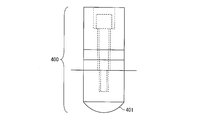
- Patent Document 1 in a compound lens molding apparatus, a high frequency voltage is applied to the molding die 400 to vibrate the molding surface 401 of the molding die 400, thereby forming the molding.
- a technique for releasing the obtained lens is disclosed. In this method, it is said that the adhesive strength of the lens with the molding surface 401 can be lowered by elastically deforming the molding surface 401, so that the mold can be safely released.
- Patent Document 1 when the method described in Patent Document 1 is applied to an aspherical lens or the like, in this method, the molding surface of the molding die is vibrated and released from the mold. There is a risk that.
- the present invention has been made to solve the above problems, and an object thereof is to realize a resin molding apparatus and a resin molding method capable of easily molding a resin molded product with high accuracy.
- a resin molding apparatus includes a first molding die having a first transfer surface for transferring a predetermined shape to a resin material that is a dielectric, and the resin.
- a second molding die having a second transfer surface for transferring a predetermined shape to the material, the second transfer surface facing the first transfer surface; and the first molding
- a moving means for changing a relative position between the mold and the second molding mold; and the resin material supplied onto the first transfer surface and pressed against the second transfer surface is cured.
- a resin molding apparatus comprising a curing means for molding a resin molded product, wherein an electric field is formed by applying a DC voltage between the first molding die and the second molding die. And a direction of the electric field from the first molding die to the second molding die. It is characterized in that it comprises a switching means for switching between from the second forming die and the direction toward the first molding die.
- the curing means in a state where the second transfer surface of the second molding die is pressed against the resin material supplied onto the first transfer surface of the first molding die.
- the resin material is molded by curing the resin material.
- an electric field is formed between the first molding die and the second molding die by the electric field forming means.
- the switching unit switches the direction of the electric field to the reverse direction, and the moving unit separates the second transfer surface from the resin molded product.
- the switching means when the direction of the electric field formed while the resin material is cured is the direction from the first molding die to the second molding die, after the resin material is solidified, the switching means The direction of the electric field is switched from the second molding die toward the first molding die. Similarly, the direction of the electric field formed while the resin material is cured is changed from the second molding die to the first molding die. In the case of the direction toward the first molding die, after the resin material is solidified, the switching unit switches the direction of the electric field from the first molding die to the second molding die.
- the first and second molding dies and the resin material repel each other. Therefore, since the adhesive force between the first and second molding dies and the resin material is reduced, the mold can be released without applying a load to the resin material. Therefore, it is possible to realize a resin molding apparatus capable of easily molding a resin molded product with high accuracy.
- a resin molding method is a method in which a second molding die is added to a resin material that is a dielectric material supplied on a first transfer surface of a first molding die.
- a resin material curing step in which the resin material is cured to form a resin molding in a state where the transfer surface of 2 is pressed, and a mold release step in which the second transfer surface is separated from the resin molding.
- an electric field in a predetermined direction is formed by applying a DC voltage between the first molding die and the second molding die, and in the releasing step, An electric field in a direction opposite to the predetermined direction is formed between one molding die and the second molding die.
- the second transfer surface of the second molding die is pressed against the resin material supplied onto the first transfer surface of the first molding die.
- the resin material is cured, and in the mold release step, the second transfer surface is separated from the resin molded product, whereby the resin molded product is molded.
- an electric field in a predetermined direction is formed between the first molding die and the second molding die in the resin material curing step, and an electric field in the opposite direction to the electric field is formed in the releasing step.
- the first and second molding dies and the resin material repel each other. Therefore, since the adhesive force between the first and second molding dies and the resin material is reduced, the mold can be released without applying a load to the resin material. Therefore, it is possible to realize a resin molding method capable of easily molding a resin molded product with high accuracy.
- the resin molding apparatus includes a first molding die having a first transfer surface for transferring a predetermined shape to a resin material that is a dielectric, and a predetermined amount applied to the resin material.
- a second molding die having a second transfer surface for transferring the shape, the second transfer surface facing the first transfer surface; the first molding die; and
- a moving means for changing the relative position with the second molding die, and the resin material supplied onto the first transfer surface and pressed against the second transfer surface are cured to obtain a resin molded product.
- a resin molding apparatus comprising a curing means for molding, wherein the electric field forming means forms an electric field by applying a DC voltage between the first molding die and the second molding die, and The direction of the electric field is changed from the first molding die toward the second molding die and the second component.
- Switch between the mold and the direction toward the first forming die is configured to include a switching unit.
- the second transfer surface of the second molding die is pressed against a resin material which is a dielectric material supplied onto the first transfer surface of the first molding die.
- a resin material curing step in which the resin material is cured to form a resin molded product, and a mold release step in which the second transfer surface is separated from the resin molded product.
- An electric field in a predetermined direction is formed by applying a DC voltage between the first molding die and the second molding die, and in the mold release step, the first molding die and the An electric field in a direction opposite to the predetermined direction is formed between the second molding die and the second molding die.
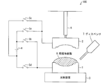
- FIG. 1 It is a figure which shows the structure of the lens shaping
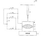
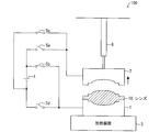
- molding apparatus shown in FIG. 1 it is a figure which shows the state which supplied dielectric resin on the transfer surface of a shaping die. It is a figure which shows the state which presses the transfer surface of a shaping die against dielectric resin, and heats dielectric resin. It is a figure which shows the charging state of a shaping die and dielectric resin, (a) shows the state before hardening of dielectric resin, (b) shows the state after hardening of dielectric resin. Yes. It is a figure which shows the state which reversed the electric field after dielectric resin solidified. It is a figure which shows the state which pulled apart the transcription
- FIGS. 1 to 10 An embodiment of the present invention will be described with reference to FIGS. 1 to 10 as follows.
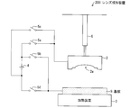
- FIG. 1 is a diagram illustrating a configuration of a lens molding apparatus (resin molding apparatus) 100 according to the present embodiment.
- the lens molding device 100 is a device for molding a lens from a dielectric resin, and includes a molding die 1, a molding die 2, a heating device 3, a DC power supply 4, four switches 5a, 5b, 5c, and 5d, and a support device 6. It has.
- the molding die 1 corresponds to the first molding die described in the claims, and is provided on the heating device 3.
- the molding die 2 corresponds to a second molding die described in the claims, and is supported above the molding die 1 by a support device 6.
- the support device 6 is an expandable member, and can move the molding die 2 up and down in the drawing.
- the support device 6 corresponds to the moving means described in the claims.
- the molding die 1 has a transfer surface 1a for transferring a predetermined lens shape to a dielectric resin, and an aspherical recess is formed at the center of the transfer surface 1a.
- the molding die 2 also has a transfer surface 2a for transferring a predetermined lens shape to the dielectric resin, and an aspherical recess is formed at the center of the transfer surface 2a.
- the transfer surface 1a and the transfer surface 2a face each other.
- the molding dies 1 and 2 also function as electrodes for forming an electric field.
- the heating device 3 corresponds to the curing means described in the claims, and cures the dielectric resin supplied onto the transfer surface 1 a of the molding die 1 by heating the molding die 1. .
- the start / end of heating may be controlled by a sequence program or the like, or may be controlled manually.
- the DC power supply 4 corresponds to the electric field forming means described in the claims.
- the DC power supply 4 is, for example, a 6 kV DC power supply, and is connected to the molding dies 1 and 2 through switches 5a, 5b, 5c, and 5d.
- the positive electrode of the DC power supply 4 is connected to the molding die 2 through the switch 5a and is connected to the molding die 1 through the switch 5b.
- the negative electrode of the DC power source 4 is connected to the molding die 2 via a switch 5c and is connected to the molding die 1 via a switch 5d.
- An electric field can be generated between the molding die 1 and the molding die 2 by controlling the ON / OFF of the switches 5a, 5b, 5c, and 5d.
- the switches 5a, 5b, 5c, and 5d correspond to switching means described in the claims.
- a dielectric resin 8 is supplied onto the transfer surface 1 a of the molding die 1 using a dispenser 7.
- the dielectric resin 8 is a thermosetting resin that cures when heated.
- the four switches 5a, 5b, 5c, and 5d are all OFF.
- the support device 6 moves the molding die 2 downward and presses the transfer surface 2 a of the molding die 2 against the dielectric resin 8.
- the switches 5a and 5d are turned ON so that the potential of the molding die 2 is higher than the potential of the molding die 1.
- an electric field from the molding die 2 toward the molding die 1 is formed between the molding die 1 and the molding die 2, so that the dielectric resin 8 is transferred to the transfer surface 2 a of the molding die 2.
- the molding die 1 is heated by the heating device 3 in a state where the transfer surface 2a of the molding die 2 is pressed against the dielectric resin 8 and an electric field from the molding die 2 toward the molding die 1 is formed. (Resin material curing step). As a result, the dielectric resin 8 is cured.
- the molding dies 1 and 2 and the dielectric resin 8 are in the charged state shown in FIG. Since the potential of the molding die 2 is higher than that of the molding die 1, the surface of the dielectric resin 8 in contact with the molding die 2 is negatively charged, and the surface of the dielectric resin 8 in contact with the molding die 1 is positive. Is charged.
- the heating is stopped, and as shown in FIG. 5, the switches 5a and 5d are turned off and the switches 5b and 5c are turned on. Thereby, the potential of the molding die 1 becomes higher than the potential of the molding die 2, and the direction of the electric field between the molding die 1 and the molding die 2 is reversed.
- the molding dies 1 and 2 and the dielectric resin 8 are in the charged state shown in FIG. Since the dielectric resin 8 is solidified, the charged state is the same as the state in the middle of curing shown in FIG. On the other hand, since the molding die 1 is positively charged and the molding die 2 is negatively charged, the molding dies 1 and 2 and the dielectric resin 8 repel each other. Therefore, the adhesive force between the molding dies 1 and 2 and the dielectric resin 8 can be greatly reduced as compared with the case where no electric field is formed.
- the support device 6 raises the molding die 2 and separates the transfer surface 2a from the dielectric resin 8 (mold release step). Thereby, the lens 18 having an aspherical shape is formed.
- the mold can be released without applying a load to the dielectric resin 8. Further, unlike the conventional configuration, it is not necessary to apply vibration in order to reduce the adhesion between the molding die and the resin molded product, so that the lens 18 without damage can be molded.
- the lens molding apparatus 100 can mold a lens having a complicated shape with high accuracy and ease. Further, the margin of the dielectric resin material is widened, a lens having a large thickness deviation and a large aspheric amount can be easily molded.
- an electric field from the molding die 2 toward the molding die 1 is formed before the dielectric resin 8 is solidified, and the direction of the electric field is changed from the molding die 1 to the molding die after the dielectric resin 8 is solidified.
- the direction which goes to 2 it is not limited to this.
- an electric field is formed from the molding die 1 toward the molding die 2
- the direction of the electric field is directed from the molding die 2 to the molding die 1. The direction may be switched.
- thermosetting resin is used as the dielectric resin 8.
- the present invention is not limited to this.
- a photocurable resin that is cured by being irradiated with UV may be used.
- a UV irradiation device is used instead of the heating device 3.
- the direction of the electric field is switched by ON / OFF control of the switches 5a to 5d.
- the present invention is not limited to this.
- a DC power source in which the positive electrode is connected to the molding die 1 a negative electrode is connected to the molding die 2
- the direction of the electric field may be switched by providing and switching the connection between the DC power source and the molding die.
- the molds 1 and 2 used for lens molding are molds for molding a single lens.
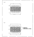
- a plurality of array lenses are molded as in the molds 11 and 12 shown in FIG. A mold may be used.
- FIG. 8 is a graph showing the temperature of the dielectric resin 8 in time series.
- the temperature of the dielectric resin 8 when the dielectric resin 8 is supplied to the molding die 1 (FIG. 2) is T1.
- T1 An electric field from the molding die 2 toward the molding die 1 is formed (FIG. 3).
- time t2 heating is started, and the temperature of the dielectric resin 8 rises to T2.
- time t3 the dielectric resin 8 is solidified.
- the timing of electric field formation and electric field inversion is not limited to the above.
- the timing for forming the electric field may be any time as long as it is until time t3 when the dielectric resin 8 is solidified.
- the timing for reversing the direction of the electric field may be any time as long as the dielectric resin 8 is solidified and then released.
- FIG. 9 is a diagram illustrating a configuration of a lens molding device 200 according to a first modification of the present embodiment.
- the lens molding apparatus 200 has a configuration in which the molding die 1 is replaced with a substrate 9 in the lens molding apparatus 100 shown in FIG.
- the substrate 9 is connected to the positive electrode of the DC power source 4 through the switch 5b, and is connected to the negative electrode of the DC power source 4 through the switch 5d.
- the lens molding process in the lens molding apparatus 200 is substantially the same as that in the lens molding apparatus 100. That is, a dielectric resin is supplied onto the substrate 9, the transfer surface 2 a of the molding die 2 is pressed against the dielectric resin, and an electric field is formed between the molding die 2 and the substrate 9. After the resin is cured and the dielectric resin is solidified, the direction of the electric field is reversed and the mold is released. Thereby, the single-sided lens which has a complicated shape can be shape
- the molding die 2 corresponds to the molding die described in the claims.
- Modification 2 In the above, an electric field is formed by applying a DC voltage between the molding dies 1 and 2 or between the molding die 2 and the substrate 9, but an AC voltage is applied instead of the DC voltage. It may be configured to.
- FIG. 10 is a diagram illustrating a configuration of a lens molding device 300 according to a second modification of the present embodiment.
- the lens molding apparatus 300 has a configuration in which the DC power supply 4 is replaced with an AC power supply 14 in the lens molding apparatus 100 shown in FIG.
- One electrode of the AC power source 14 is connected to the molding die 2 via the switch 5e, and the other electrode of the AC power source 14 is directly connected to the molding die 1.
- the switch 5e is turned on, and an AC voltage is applied between the molding die 1 and the molding die 2. Apply. In this state, the transfer surface 2a of the molding die 2 is pressed against the dielectric resin, and the dielectric resin is heated. The application of the AC voltage is continued until the dielectric resin is solidified and released.
- the dielectric resin is attracted to the transfer surface 2a of the molding die 2 until the dielectric resin is solidified by application of AC voltage.
- the polarity of the molding dies 1 and 2 is constantly reversed, so that the dipole on the surface of the dielectric resin causes the electric field between the molding dies 1 and 2.
- the adhesive force between the molding dies 1 and 2 and the dielectric resin is reduced, so that the mold release can be easily performed.
- the structure to apply may be sufficient.
- a resin molding apparatus includes a substrate, a molding die having a transfer surface for transferring a predetermined shape to a resin material that is a dielectric, and a relative position between the molding die and the substrate.
- a resin molding apparatus comprising: a moving unit that changes the thickness of the resin material; and a curing unit that cures the resin material supplied onto the substrate and pressed against the transfer surface to mold a resin molded product.
- Electric field forming means for forming an electric field by applying a DC voltage between the mold and the substrate, the direction of the electric field from the molding die toward the substrate, and from the substrate to the molding die And switching means for switching between the directions.
- the resin molding is molded by the curing means curing the resin material in a state where the transfer surface of the molding die is pressed against the resin material supplied onto the substrate.
- an electric field is formed between the substrate and the molding die by the electric field forming means.
- the direction of the electric field is switched to the reverse direction by the switching unit, and the transfer surface is pulled away from the resin molding by the moving unit. That is, when the direction of the electric field formed while the resin material is cured is the direction from the substrate to the molding die, after the resin material is solidified, the switching unit changes the direction of the electric field from the molding die.
- the switching means The direction of the electric field is switched from the substrate to the molding die.
- the substrate, the mold and the resin material repel each other. Therefore, since the adhesive force between the substrate and the molding die and the resin material is reduced, the mold can be released without applying a load to the resin material.
- a resin molding apparatus includes a first molding die having a first transfer surface for transferring a predetermined shape to a resin material that is a dielectric, and a predetermined shape for the resin material.
- a second molding die having a second transfer surface for transferring, the second transfer surface facing the first transfer surface, the first molding die and the second And a moving means for changing the relative position of the molding die, and the resin material supplied onto the first transfer surface and pressed against the second transfer surface is cured to mold a resin molded product.
- a resin molding apparatus including a curing unit, comprising: an electric field forming unit that forms an electric field by applying an alternating voltage between the first molding die and the second molding die.
- the curing means in a state where the second transfer surface of the second molding die is pressed against the resin material supplied onto the first transfer surface of the first molding die.
- the resin material is molded by curing the resin material.
- the electric field forming unit applies an AC voltage between the first molding die and the second molding die,
- the polarities of the first and second molding dies are constantly reversed.
- the dipole on the surface of the resin material moves following the reversal of the electric field between the first molding die and the second molding die. Due to the movement of the dipole, the adhesive force between the first and second molding dies and the resin material is reduced, so that the mold can be easily released.
- a resin molding apparatus includes a substrate, a molding die having a transfer surface for transferring a predetermined shape to a resin material that is a dielectric, and a relative position between the molding die and the substrate.
- a resin molding apparatus comprising: a moving unit that changes the thickness of the resin material; and a curing unit that cures the resin material supplied onto the substrate and pressed against the transfer surface to mold a resin molded product.
- Electric field forming means for forming an electric field by applying an alternating voltage between the mold and the substrate is provided.
- the resin molding is molded by the curing means curing the resin material in a state where the transfer surface of the molding die is pressed against the resin material supplied onto the substrate.
- the electric field forming means applies an alternating voltage between the substrate and the molding die, so that the polarities of the substrate and the molding die are constantly reversed.
- the dipole on the surface of the resin material moves following the reversal of the electric field between the substrate and the molding die. Due to the movement of the dipole, the adhesive force between the substrate and the molding die and the resin material is reduced, so that the mold can be easily released.
- a resin molding method molds a resin molding by curing the resin material in a state where the transfer surface of a molding die is pressed against a resin material which is a dielectric material supplied onto a substrate.
- a DC voltage is applied between the substrate and the molding die.
- An electric field in a predetermined direction is formed, and in the releasing step, an electric field in a direction opposite to the predetermined direction is formed between the substrate and the molding die.
- the resin material curing step the resin material is cured in a state in which the transfer surface of the molding die is pressed against the resin material supplied onto the substrate.
- the resin molded product is molded by pulling away from the resin molded product.
- an electric field in a predetermined direction is formed between the substrate and the molding die in the resin material curing step, and an electric field in the opposite direction to the electric field is formed in the mold releasing step.
- the substrate, the mold and the resin material repel each other. Therefore, since the adhesive force between the substrate and the molding die and the resin material is reduced, the mold can be released without applying a load to the resin material.
- the second transfer surface of the second molding die is pressed against the resin material that is a dielectric material supplied onto the first transfer surface of the first molding die.
- the resin material is cured to form a resin molded product, and the resin material is cured, and the second transfer surface is separated from the resin molded product.
- An AC voltage is applied between the first molding die and the second molding die.
- the second transfer surface of the second molding die is pressed against the resin material supplied onto the first transfer surface of the first molding die.
- the resin material is cured, and in the mold release step, the second transfer surface is separated from the resin molded product, whereby the resin molded product is molded.
- the polarity of the first and second molding dies is constantly reversed by applying an AC voltage between the first molding die and the second molding die.
- the dipole on the surface of the resin material moves following the reversal of the electric field between the first molding die and the second molding die. Due to the movement of the dipole, the adhesive force between the first and second molding dies and the resin material is reduced, so that the mold can be easily released.
- a resin molding method molds a resin molding by curing the resin material in a state where the transfer surface of a molding die is pressed against a resin material which is a dielectric material supplied onto a substrate.
- the resin material curing step the resin material is cured in a state in which the transfer surface of the molding die is pressed against the resin material supplied onto the substrate.
- the resin molded product is molded by pulling away from the resin molded product.
- the mold release step the polarity of the substrate and the molding die is constantly reversed by applying an alternating voltage between the substrate and the molding die.
- the dipole on the surface of the resin material moves following the reversal of the electric field between the substrate and the molding die. Due to the movement of the dipole, the adhesive force between the substrate and the molding die and the resin material is reduced, so that the mold can be easily released.
- the resin molded product is preferably one or a plurality of lenses.
- the present invention can be released without applying a load to the resin material, and thus is particularly suitable for molding a lens having a complicated shape.
- the present invention can be applied not only to a lens molding apparatus but also to an apparatus for molding any resin molding other than a lens.
- first mold 1a Transfer surface (first transfer surface) 2 Mold (molding die, second molding die) 2a Transfer surface (transfer surface, second transfer surface) 3 Heating device (curing means) 4 DC power supply (electric field forming means) 5a switch (switching means) 5b switch (switching means) 5c switch (switching means) 5d switch (switching means) 5e switch 6 support device (moving means) 7 Dispenser 8 Dielectric resin (resin material) 9 Substrate 11 Mold (first mold) 12 Mold (second mold) 14 AC power supply (electric field forming means) 18 Lens (resin molding) 100 Lens molding equipment (resin molding equipment) 200 Lens molding equipment (resin molding equipment) 300 Lens molding equipment (resin molding equipment)
Landscapes
- Engineering & Computer Science (AREA)
- Mechanical Engineering (AREA)
- Health & Medical Sciences (AREA)
- Manufacturing & Machinery (AREA)
- Ophthalmology & Optometry (AREA)
- Moulds For Moulding Plastics Or The Like (AREA)
- Casting Or Compression Moulding Of Plastics Or The Like (AREA)
Abstract
本発明に係るレンズ成形装置(100)は、誘電体樹脂に所定のレンズ形状を転写するための転写面(1a)を有する成形金型(1)と、誘電体樹脂に所定のレンズ形状を転写するための転写面(2a)を有する成形金型(2)と、成形金型(2)を移動させる支持装置(6)と、転写面(1a)上に供給された誘電体樹脂を加熱することにより樹脂成形物を成形する加熱装置(3)と、成形金型(1)と成形金型(2)との間に直流電圧を印加することにより電界を形成する直流電源(4)と、前記電界の方向を、成形金型(1)から成形金型(2)に向かう方向と、成形金型(2)から成形金型(1)に向かう方向との間で切り替えるスイッチ(5a~5d)とを備える。
Description
本発明は、樹脂成形装置および樹脂成形方法に関し、特に、複雑な形状を有するレンズを高精度かつ容易に成形可能なレンズ成形装置およびレンズ成形方法に関する。
従来より、レンズ形状を転写するための転写面を有する金型を樹脂材料に押し当て、その状態で樹脂材料を硬化させることにより、レンズを成形するレンズ成形方法が用いられている。当該レンズ成形方法では、樹脂材料を硬化させた後、レンズから離型させるときに、レンズと転写面との間の付着力により、レンズが損傷してしまうおそれがある。
これに対し、特許文献1には、図11に示すように、複合レンズの成形装置において、高周波の電圧を成形金型400に印加して成形金型400の成形面401を振動させて、成形したレンズを離型する技術が開示されている。この方法では、成形面401を弾性変形させることにより、レンズの成形面401との密着強度を下げることができるので、安全に離型することができるとされている。
光学系の高性能化に伴い、複雑な形状を有する薄肉のレンズを高精度に加工する技術が重要となっている。特に、薄肉であって偏肉性および非球面量が大きいレンズは、十分な剛性を確保することができないため、成形型に付着したレンズを剥す際の負荷により、レンズ自体に変形や割れなどの損傷を生じるおそれがある。そのため、非球面レンズ等の成形では、成形物と成形金型との抵抗を極力少なくすることが要求され、離型が難しいという問題がある。
しかしながら、特許文献1に記載の方法を非球面レンズ等に適用した場合、当該方法では成形金型の成形面を振動させて離型するため、振動によってレンズに変形や割れなどの損傷を与えてしまうおそれがある。
本発明は、上記の問題点を解決するためになされたもので、その目的は、樹脂成形物を高精度かつ容易に成形可能な樹脂成形装置および樹脂成形方法を実現することにある。
上記の課題を解決するために、本発明に係る樹脂成形装置は、誘電体である樹脂材料に所定の形状を転写するための第1の転写面を有する第1の成形金型と、前記樹脂材料に所定の形状を転写するための第2の転写面を有し、当該第2の転写面が前記第1の転写面と対向している第2の成形金型と、前記第1の成形金型と前記第2の成形金型との相対位置を変化させる移動手段と、前記第1の転写面上に供給され、前記第2の転写面が押し当てられた前記樹脂材料を硬化させて樹脂成形物を成形する硬化手段とを備える樹脂成形装置であって、前記第1の成形金型と前記第2の成形金型との間に直流電圧を印加することにより電界を形成する電界形成手段と、前記電界の方向を、前記第1の成形金型から前記第2の成形金型に向かう方向と、前記第2の成形金型から前記第1の成形金型に向かう方向との間で切り替える切替手段とを備えることを特徴としている。
上記の構成によれば、第1の成形金型の第1の転写面上に供給された樹脂材料に、第2の成形金型の第2の転写面が押し当てられた状態で、硬化手段が樹脂材料を硬化させることにより、樹脂成形物が成形される。ここで、樹脂材料が硬化されている間に、電界形成手段によって第1の成形金型と第2の成形金型との間に電界を形成する。続いて、樹脂材料が固化した後、切替手段によって、電界の方向を逆方向に切り替えて、移動手段によって樹脂成形物から第2の転写面を引き離す。すなわち、樹脂材料が硬化されている間に形成された電界の方向が第1の成形金型から第2の成形金型に向かう方向である場合、樹脂材料が固化した後、切替手段は、当該電界の方向を第2の成形金型から第1の成形金型に向かう方向に切り替え、同様に、樹脂材料が硬化されている間に形成された電界の方向が第2の成形金型から第1の成形金型に向かう方向である場合、樹脂材料が固化した後、切替手段は、当該電界の方向を第1の成形金型から第2の成形金型に向かう方向に切り替える。
樹脂材料が固化すると、その帯電状態は固定されるため、電界の方向を樹脂材料が固化した後に反転させると、第1および第2の成形金型と樹脂材料とが、互いに反発する。そのため、第1および第2の成形金型と樹脂材料との間の付着力が低下するので、樹脂材料へ負荷をかけることなく離型することができる。したがって、樹脂成形物を高精度かつ容易に成形可能な樹脂成形装置を実現することができる。
上記の課題を解決するために、本発明に係る樹脂成形方法は、第1の成形金型の第1の転写面上に供給された誘電体である樹脂材料に第2の成形金型の第2の転写面を押し当てた状態で、前記樹脂材料を硬化させて樹脂成形物を成形する樹脂材料硬化工程と、前記第2の転写面を前記樹脂成形物から引き離す離型工程とを有し、前記樹脂材料硬化工程では、前記第1の成形金型と前記第2の成形金型との間に直流電圧を印加することにより所定方向の電界を形成し、前記離型工程では、前記第1の成形金型と前記第2の成形金型との間に前記所定方向とは反対方向の電界を形成することを特徴としている。
上記の構成によれば、樹脂材料硬化工程において、第1の成形金型の第1の転写面上に供給された樹脂材料に、第2の成形金型の第2の転写面が押し当てられた状態で、樹脂材料を硬化させ、離型工程において、第2の転写面を前記樹脂成形物から引き離すことで、樹脂成形物が成形される。ここで、樹脂材料硬化工程において、第1の成形金型と第2の成形金型との間に所定方向の電界を形成し、離型工程において、当該電界と逆方向の電界を形成する。
樹脂材料が固化すると、その帯電状態は固定されるため、電界の方向を樹脂材料が固化した後に反転させると、第1および第2の成形金型と樹脂材料とが、互いに反発する。そのため、第1および第2の成形金型と樹脂材料との間の付着力が低下するので、樹脂材料へ負荷をかけることなく離型することができる。したがって、樹脂成形物を高精度かつ容易に成形可能な樹脂成形方法を実現することができる。
以上のように、本発明に係る樹脂成形装置は、誘電体である樹脂材料に所定の形状を転写するための第1の転写面を有する第1の成形金型と、前記樹脂材料に所定の形状を転写するための第2の転写面を有し、当該第2の転写面が前記第1の転写面と対向している第2の成形金型と、前記第1の成形金型と前記第2の成形金型との相対位置を変化させる移動手段と、前記第1の転写面上に供給され、前記第2の転写面が押し当てられた前記樹脂材料を硬化させて樹脂成形物を成形する硬化手段とを備える樹脂成形装置であって、前記第1の成形金型と前記第2の成形金型との間に直流電圧を印加することにより電界を形成する電界形成手段と、前記電界の方向を、前記第1の成形金型から前記第2の成形金型に向かう方向と、前記第2の成形金型から前記第1の成形金型に向かう方向との間で切り替える切替手段とを備える構成である。また、本発明に係る樹脂成形方法は、第1の成形金型の第1の転写面上に供給された誘電体である樹脂材料に第2の成形金型の第2の転写面を押し当てた状態で、前記樹脂材料を硬化させて樹脂成形物を成形する樹脂材料硬化工程と、前記第2の転写面を前記樹脂成形物から引き離す離型工程とを有し、前記樹脂材料硬化工程では、前記第1の成形金型と前記第2の成形金型との間に直流電圧を印加することにより所定方向の電界を形成し、前記離型工程では、前記第1の成形金型と前記第2の成形金型との間に前記所定方向とは反対方向の電界を形成する構成である。
したがって、樹脂成形物を高精度かつ容易に成形可能な樹脂成形装置および樹脂成形方法を実現できるという効果を奏する。
本発明の実施の一形態について、図1~図10に基づいて説明すれば以下のとおりである。
(レンズ成形装置の構成)
図1は、本実施形態に係るレンズ成形装置(樹脂成形装置)100の構成を示す図である。レンズ成形装置100は、誘電体樹脂からレンズを成形する装置であり、成形金型1、成形金型2、加熱装置3、直流電源4、4つのスイッチ5a・5b・5c・5dおよび支持装置6を備えている。
図1は、本実施形態に係るレンズ成形装置(樹脂成形装置)100の構成を示す図である。レンズ成形装置100は、誘電体樹脂からレンズを成形する装置であり、成形金型1、成形金型2、加熱装置3、直流電源4、4つのスイッチ5a・5b・5c・5dおよび支持装置6を備えている。
成形金型1は、特許請求の範囲に記載の第1の成形金型に相当するものであり、加熱装置3上に設けられている。また、成形金型2は、特許請求の範囲に記載の第2の成形金型に相当するものであり、支持装置6によって成形金型1の上方に支持されている。支持装置6は、伸縮可能な部材であり、成形金型2を図中上下に移動させることができる。なお、支持装置6は、特許請求の範囲に記載の移動手段に相当する。
成形金型1は、誘電体樹脂に所定のレンズ形状を転写するための転写面1aを有しており、転写面1aの中心部には、非球面形状の凹部が形成されている。同様に、成形金型2も、誘電体樹脂に所定のレンズ形状を転写するための転写面2aを有しており、転写面2aの中心部には、非球面形状の凹部が形成されている。転写面1aと転写面2aとは、互いに対向している。また、成形金型1・2は、電界を形成するための電極としても機能する。
加熱装置3は、特許請求の範囲に記載の硬化手段に相当するものであり、成形金型1を加熱することにより、成形金型1の転写面1a上に供給された誘電体樹脂を硬化させる。加熱の開始/終了は、シーケンスプログラム等によって制御してもよいし、手動で制御してもよい。
直流電源4は、特許請求の範囲に記載の電界形成手段に相当するものである。直流電源4は、例えば6kVの直流電源であり、スイッチ5a・5b・5c・5dを介して成形金型1・2に接続されている。具体的には、直流電源4の正極は、スイッチ5aを介して成形金型2に接続され、スイッチ5bを介して成形金型1に接続されている。また、直流電源4の負極は、スイッチ5cを介して成形金型2に接続され、スイッチ5dを介して成形金型1に接続されている。各スイッチ5a・5b・5c・5dのON/OFFを制御することにより、成形金型1と成形金型2との間に電界を発生させることができる。なお、スイッチ5a・5b・5c・5dは、特許請求の範囲に記載の切替手段に相当する。
(レンズの成形工程)
続いて、レンズ成形装置100におけるレンズの成形工程について、図2~図5を参照して説明する。
続いて、レンズ成形装置100におけるレンズの成形工程について、図2~図5を参照して説明する。
まず、図2に示すように、ディスペンサ7を用いて、成形金型1の転写面1a上に誘電体樹脂8を供給する。誘電体樹脂8は、加熱されることにより硬化する熱硬化性樹脂である。なお、このとき4つのスイッチ5a・5b・5c・5dはいずれもOFFである。
続いて、図3に示すように、支持装置6が成形金型2を下方に移動させて、成形金型2の転写面2aを誘電体樹脂8に押し当てる。このとき、スイッチ5a・5dをONにして、成形金型2の電位を成形金型1の電位よりも高くする。これにより、成形金型1と成形金型2との間には、成形金型2から成形金型1に向かう電界が形成されるため、誘電体樹脂8は、成形金型2の転写面2aに引き寄せられる。よって、転写面2aと誘電体樹脂8との間に気泡がほとんど発生せず、転写面2aの形状を誘電体樹脂8に高精度に転写することができる。
さらに、成形金型2の転写面2aが誘電体樹脂8に押し当てられ、成形金型2から成形金型1に向かう電界が形成された状態で、加熱装置3により成形金型1を加熱する(樹脂材料硬化工程)。これにより、誘電体樹脂8が硬化する。
このとき、成形金型1・2および誘電体樹脂8は、図4の(a)に示す帯電状態になる。成形金型2の電位が成形金型1の電位よりも高いため、誘電体樹脂8の成形金型2と接する表面は負に帯電し、誘電体樹脂8の成形金型1と接する表面は正に帯電している。
誘電体樹脂8の固化した後、加熱を停止し、図5に示すように、スイッチ5a・5dをOFFにして、スイッチ5b・5cをONにする。これにより、成形金型1の電位が成形金型2の電位よりも高くなり、成形金型1と成形金型2との間の電界の向きが反転する。
このとき、成形金型1・2および誘電体樹脂8は、図4の(b)に示す帯電状態になる。誘電体樹脂8は固化しているため、帯電状態は図4の(a)に示す硬化途中の状態と同一である。一方、成形金型1が正に帯電し、成形金型2が負に帯電しているため、成形金型1・2と誘電体樹脂8とは、互いに反発する。そのため、成形金型1・2と誘電体樹脂8との間の付着力を、電界を形成しない場合に比べて大幅に低減することができる。
この状態で、図6に示すように、支持装置6が成形金型2を上昇させ、転写面2aを誘電体樹脂8から引き離す(離型工程)。これにより、非球面形状を有するレンズ18が形成される。上記のように、電界形成により、成形金型2と誘電体樹脂8との間の付着力が低下しているので、誘電体樹脂8へ負荷をかけることなく離型することができる。また、従来構成のように、成形金型と樹脂成形物との間の付着力を低下させるために振動を与える必要がないので、損傷のないレンズ18を成形することができる。
このように、本実施形態に係るレンズ成形装置100は、複雑な形状を有するレンズを高精度かつ容易に成形することができる。また、誘電体樹脂の材料のマージンが広がり、偏肉性が大きく、非球面量が大きなレンズも容易に成形することができる。
上記では、誘電体樹脂8が固化する前に、成形金型2から成形金型1に向かう電界を形成し、誘電体樹脂8が固化した後に、電界の方向を成形金型1から成形金型2に向かう方向に切り替えたが、これに限定されない。誘電体樹脂8が固化する前に、成形金型1から成形金型2に向かう電界を形成し、誘電体樹脂8が固化した後に、電界の方向を成形金型2から成形金型1に向かう方向に切り替えてもよい。
また、上記では、誘電体樹脂8として熱硬化性樹脂を用いたが、これに限定されず、例えば、UVを照射されることにより硬化する光硬化性樹脂を用いてもよい。この場合、加熱装置3の代わりに、UV照射装置が用いられる。
また、上記では、スイッチ5a~5dのON/OFF制御によって、電界の方向の切り替えを行っていたが、本発明はこれに限定されない。例えば、正極が成形金型1に接続され、負極が成形金型2に接続された直流電源と、負極が成形金型1に接続され、正極が成形金型2に接続された直流電源とを設け、それらの直流電源と成形金型との接続を切り替えることにより、電界の方向の切り替えを行ってもよい。
また、レンズ成形に用いられる成形金型1・2は、1つのレンズを成形する金型であったが、例えば図7に示す成形金型11・12のように、複数のアレイレンズを成形する金型を用いてもよい。
(電界形成および電界反転のタイミング)
続いて、成形金型1・2間の電界形成および電界反転のタイミングの一例について説明する。
続いて、成形金型1・2間の電界形成および電界反転のタイミングの一例について説明する。
図8は、誘電体樹脂8の温度を時系列的に示したグラフである。誘電体樹脂8を成形金型1に供給した時点(図2)における誘電体樹脂8の温度はT1である。時間t1において、成形金型2から成形金型1に向かう電界を形成する(図3)。その後、時間t2において、加熱を開始し、誘電体樹脂8の温度はT2に上昇する。その後、時間t3において、誘電体樹脂8が固化する。
その後、時間t4において、冷却開始と同時に電界の方向を成形金型1から成形金型2に向かう方向に反転させる(図5)。これにより、成形金型1・2と誘電体樹脂8とを引き剥がす力が働き、成形金型1・2と誘電体樹脂8との間の付着力が低下する。冷却完了後、時間t5において、成形金型2を上方に移動させて、成形されたレンズ18を取り出す(図6)。
電界形成および電界反転のタイミングは上記に限定されない。電界を形成するタイミングは、誘電体樹脂8が固化する時間t3までであれば、いつでもよい。また、電界の向きを反転させるタイミングは、誘電体樹脂8が固化してから離型するまでの間であれば、いつでもよい。
(変形例1)
続いて、本実施形態の変形例について説明する。なお、説明の便宜上、既に説明した部材と同じ機能を有する部材については、同じ符号を付記し、その説明を省略する。
続いて、本実施形態の変形例について説明する。なお、説明の便宜上、既に説明した部材と同じ機能を有する部材については、同じ符号を付記し、その説明を省略する。
図9は、本実施形態の第1の変形例に係るレンズ成形装置200の構成を示す図である。レンズ成形装置200は、図1に示すレンズ成形装置100において、成形金型1を基板9に置き換えた構成である。基板9は、スイッチ5bを介して直流電源4の正極に接続され、スイッチ5dを介して直流電源4の負極に接続されている。
レンズ成形装置200におけるレンズの成形工程は、レンズ成形装置100におけるものと略同一である。すなわち、基板9上に誘電体樹脂を供給して、成形金型2の転写面2aを誘電体樹脂に押し当て、成形金型2と基板9との間に電界を形成した状態で、誘電体樹脂を硬化させ、誘電体樹脂が固化した後、電界の向きを反転させ、離型する。これにより、複雑な形状を有する片面レンズを高精度かつ容易に成形することができる。
なお、本変形例では、成形金型2は、特許請求の範囲に記載の成形金型に相当する。
(変形例2)
上記では、成形金型1・2の間、または、成形金型2と基板9との間に、直流電圧を印加することで電界を形成していたが、直流電圧の代わりに交流電圧を印加する構成であってもよい。
上記では、成形金型1・2の間、または、成形金型2と基板9との間に、直流電圧を印加することで電界を形成していたが、直流電圧の代わりに交流電圧を印加する構成であってもよい。
図10は、本実施形態の第2の変形例に係るレンズ成形装置300の構成を示す図である。レンズ成形装置300は、図1に示すレンズ成形装置100において、直流電源4を交流電源14に置き換えた構成である。交流電源14の一方の電極は、スイッチ5eを介して成形金型2に接続され、交流電源14の他方の電極は、成形金型1に直接接続されている。
レンズ成形装置300におけるレンズの成形工程では、成形金型1の転写面1a上に誘電体樹脂を供給後、スイッチ5eをONにして、成形金型1と成形金型2との間に交流電圧を印加する。その状態で、成形金型2の転写面2aを誘電体樹脂に押し当て、誘電体樹脂を加熱する。交流電圧の印加は、誘電体樹脂が固化して離型するまで継続される。
交流電圧の印加により、誘電体樹脂が固化するまでは、誘電体樹脂は、成形金型2の転写面2aに引き寄せられる。一方、誘電体樹脂が固化した後は、成形金型1・2の極性が絶えず反転することによって、誘電体樹脂の表面の双極子が、成形金型1と成形金型2との間の電界の反転に追従して運動する。この双極子の運動によって、成形金型1・2と誘電体樹脂との間の付着力が低下するため、離型を容易に行うことができる。
なお、交流電圧の印加は、離型時のみ行ってもよい。また、誘電体樹脂が固化するまでは、成形金型1と成形金型2との間に直流電圧を印加し、離型時には、成形金型1と成形金型2との間に交流電圧を印加する構成であってもよい。
(付記事項)
本発明は上述した実施形態に限定されるものではなく、請求項に示した範囲で種々の変更が可能である。すなわち、請求項に示した範囲で適宜変更した技術的手段を組み合わせて得られる実施形態についても本発明の技術的範囲に含まれる。
本発明は上述した実施形態に限定されるものではなく、請求項に示した範囲で種々の変更が可能である。すなわち、請求項に示した範囲で適宜変更した技術的手段を組み合わせて得られる実施形態についても本発明の技術的範囲に含まれる。
本発明の実施形態に係る樹脂成形装置は、基板と、誘電体である樹脂材料に所定の形状を転写するための転写面を有する成形金型と、前記成形金型と前記基板との相対位置を変化させる移動手段と、前記基板上に供給され、前記転写面が押し当てられた前記樹脂材料を硬化させて樹脂成形物を成形する硬化手段とを備える樹脂成形装置であって、前記成形金型と前記基板との間に直流電圧を印加することにより電界を形成する電界形成手段と、前記電界の方向を、前記成形金型から前記基板に向かう方向と、前記基板から前記成形金型に向かう方向との間で切り替える切替手段とを備える。
上記の構成によれば、基板上に供給された樹脂材料に成形金型の転写面が押し当てられた状態で、硬化手段が樹脂材料を硬化させることにより、樹脂成形物が成形される。ここで、樹脂材料が硬化されている間に、電界形成手段によって基板と成形金型との間に電界を形成する。続いて、樹脂材料が固化した後、切替手段によって、電界の方向を逆方向に切り替えて、移動手段によって樹脂成形物から転写面を引き離す。すなわち、樹脂材料が硬化されている間に形成された電界の方向が基板から成形金型に向かう方向である場合、樹脂材料が固化した後、切替手段は、当該電界の方向を成形金型から基板に向かう方向に切り替え、同様に、樹脂材料が硬化されている間に形成された電界の方向が成形金型から基板に向かう方向である場合、樹脂材料が固化した後、切替手段は、当該電界の方向を基板から成形金型に向かう方向に切り替える。
樹脂材料が固化すると、その帯電状態は固定されるため、電界の方向を樹脂材料が固化した後に反転させると、基板および成形金型と樹脂材料とが、互いに反発する。そのため、基板および成形金型と樹脂材料との間の付着力が低下するので、樹脂材料へ負荷をかけることなく離型することができる。
本発明の実施形態に係る樹脂成形装置は、誘電体である樹脂材料に所定の形状を転写するための第1の転写面を有する第1の成形金型と、前記樹脂材料に所定の形状を転写するための第2の転写面を有し、当該第2の転写面が前記第1の転写面と対向している第2の成形金型と、前記第1の成形金型と前記第2の成形金型との相対位置を変化させる移動手段と、前記第1の転写面上に供給され、前記第2の転写面が押し当てられた前記樹脂材料を硬化させて樹脂成形物を成形する硬化手段とを備える樹脂成形装置であって、前記第1の成形金型と前記第2の成形金型との間に交流電圧を印加することにより電界を形成する電界形成手段を備える。
上記の構成によれば、第1の成形金型の第1の転写面上に供給された樹脂材料に、第2の成形金型の第2の転写面が押し当てられた状態で、硬化手段が樹脂材料を硬化させることにより、樹脂成形物が成形される。ここで、移動手段によって樹脂成形物から第2の転写面を引き離す際に、電界形成手段が、第1の成形金型と第2の成形金型との間に交流電圧を印加することにより、第1および第2の成形金型の極性が絶えず反転する。これに伴い、樹脂材料の表面の双極子が、第1の成形金型と第2の成形金型との間の電界の反転に追従して運動する。この双極子の運動によって、第1および第2の成形金型と樹脂材料との間の付着力が低下するため、離型を容易に行うことができる。
本発明の実施形態に係る樹脂成形装置は、基板と、誘電体である樹脂材料に所定の形状を転写するための転写面を有する成形金型と、前記成形金型と前記基板との相対位置を変化させる移動手段と、前記基板上に供給され、前記転写面が押し当てられた前記樹脂材料を硬化させて樹脂成形物を成形する硬化手段とを備える樹脂成形装置であって、前記成形金型と前記基板との間に交流電圧を印加することにより電界を形成する電界形成手段を備える。
上記の構成によれば、基板上に供給された樹脂材料に成形金型の転写面が押し当てられた状態で、硬化手段が樹脂材料を硬化させることにより、樹脂成形物が成形される。ここで、移動手段によって樹脂成形物から転写面を引き離す際に、電界形成手段が、基板と成形金型との間に交流電圧を印加することにより、基板および成形金型の極性が絶えず反転する。これに伴い、樹脂材料の表面の双極子が、基板と成形金型との間の電界の反転に追従して運動する。この双極子の運動によって、基板および成形金型と樹脂材料との間の付着力が低下するため、離型を容易に行うことができる。
本発明の実施形態に係る樹脂成形方法は、基板上に供給された誘電体である樹脂材料に成形金型の転写面を押し当てた状態で、前記樹脂材料を硬化させて樹脂成形物を成形する樹脂材料硬化工程と、前記転写面を前記樹脂成形物から引き離す離型工程とを有し、前記樹脂材料硬化工程では、前記基板と前記成形金型との間に直流電圧を印加することにより所定方向の電界を形成し、前記離型工程では、前記基板と前記成形金型との間に前記所定方向とは反対方向の電界を形成する。
上記の構成によれば、樹脂材料硬化工程において、基板上に供給された樹脂材料に、成形金型の転写面が押し当てられた状態で、樹脂材料を硬化させ、離型工程において、転写面を前記樹脂成形物から引き離すことで、樹脂成形物が成形される。ここで、樹脂材料硬化工程において、基板と成形金型との間に所定方向の電界を形成し、離型工程において、当該電界と逆方向の電界を形成する。
樹脂材料が固化すると、その帯電状態は固定されるため、電界の方向を樹脂材料が固化した後に反転させると、基板および成形金型と樹脂材料とが、互いに反発する。そのため、基板および成形金型と樹脂材料との間の付着力が低下するので、樹脂材料へ負荷をかけることなく離型することができる。
本発明の実施形態に係る樹脂成形方法は、第1の成形金型の第1の転写面上に供給された誘電体である樹脂材料に第2の成形金型の第2の転写面を押し当てた状態で、前記樹脂材料を硬化させて樹脂成形物を成形する樹脂材料硬化工程と、前記第2の転写面を前記樹脂成形物から引き離す離型工程とを有し、前記離型工程では、前記第1の成形金型と前記第2の成形金型との間に交流電圧を印加する。
上記の構成によれば、樹脂材料硬化工程において、第1の成形金型の第1の転写面上に供給された樹脂材料に、第2の成形金型の第2の転写面が押し当てられた状態で、樹脂材料を硬化させ、離型工程において、第2の転写面を前記樹脂成形物から引き離すことで、樹脂成形物が成形される。ここで、離型工程において、第1の成形金型と第2の成形金型との間に交流電圧を印加することにより、第1および第2の成形金型の極性が絶えず反転する。これに伴い、樹脂材料の表面の双極子が、第1の成形金型と第2の成形金型との間の電界の反転に追従して運動する。この双極子の運動によって、第1および第2の成形金型と樹脂材料との間の付着力が低下するため、離型を容易に行うことができる。
本発明の実施形態に係る樹脂成形方法は、基板上に供給された誘電体である樹脂材料に成形金型の転写面を押し当てた状態で、前記樹脂材料を硬化させて樹脂成形物を成形する樹脂材料硬化工程と、前記転写面を前記樹脂成形物から引き離す離型工程とを有し、前記離型工程では、前記基板と前記成形金型との間に交流電圧を印加する。
上記の構成によれば、樹脂材料硬化工程において、基板上に供給された樹脂材料に、成形金型の転写面が押し当てられた状態で、樹脂材料を硬化させ、離型工程において、転写面を前記樹脂成形物から引き離すことで、樹脂成形物が成形される。ここで、離型工程において、基板と成形金型との間に交流電圧を印加することにより、基板および成形金型の極性が絶えず反転する。これに伴い、樹脂材料の表面の双極子が、基板と成形金型との間の電界の反転に追従して運動する。この双極子の運動によって、基板および成形金型と樹脂材料との間の付着力が低下するため、離型を容易に行うことができる。
本発明の実施形態に係る樹脂成形装置および樹脂成形方法では、前記樹脂成形物は、1または複数のレンズであることが好ましい。
上記のように、本発明は、樹脂材料に負荷をかけることなく離型することができるので、複雑な形状を有するレンズの成形に特に好適である。
本発明は、レンズ成形装置だけでなく、レンズ以外のあらゆる樹脂成形物を成形するための装置に適用することができる。
1 成形金型(第1の成形金型)
1a 転写面(第1の転写面)
2 成形金型(成形金型、第2の成形金型)
2a 転写面(転写面、第2の転写面)
3 加熱装置(硬化手段)
4 直流電源(電界形成手段)
5a スイッチ(切替手段)
5b スイッチ(切替手段)
5c スイッチ(切替手段)
5d スイッチ(切替手段)
5e スイッチ
6 支持装置(移動手段)
7 ディスペンサ
8 誘電体樹脂(樹脂材料)
9 基板
11 成形金型(第1の成形金型)
12 成形金型(第2の成形金型)
14 交流電源(電界形成手段)
18 レンズ(樹脂成形物)
100 レンズ成形装置(樹脂成形装置)
200 レンズ成形装置(樹脂成形装置)
300 レンズ成形装置(樹脂成形装置)
1a 転写面(第1の転写面)
2 成形金型(成形金型、第2の成形金型)
2a 転写面(転写面、第2の転写面)
3 加熱装置(硬化手段)
4 直流電源(電界形成手段)
5a スイッチ(切替手段)
5b スイッチ(切替手段)
5c スイッチ(切替手段)
5d スイッチ(切替手段)
5e スイッチ
6 支持装置(移動手段)
7 ディスペンサ
8 誘電体樹脂(樹脂材料)
9 基板
11 成形金型(第1の成形金型)
12 成形金型(第2の成形金型)
14 交流電源(電界形成手段)
18 レンズ(樹脂成形物)
100 レンズ成形装置(樹脂成形装置)
200 レンズ成形装置(樹脂成形装置)
300 レンズ成形装置(樹脂成形装置)
Claims (10)
- 誘電体である樹脂材料に所定の形状を転写するための第1の転写面を有する第1の成形金型と、
前記樹脂材料に所定の形状を転写するための第2の転写面を有し、当該第2の転写面が前記第1の転写面と対向している第2の成形金型と、
前記第1の成形金型と前記第2の成形金型との相対位置を変化させる移動手段と、
前記第1の転写面上に供給され、前記第2の転写面が押し当てられた前記樹脂材料を硬化させて樹脂成形物を成形する硬化手段とを備える樹脂成形装置であって、
前記第1の成形金型と前記第2の成形金型との間に直流電圧を印加することにより電界を形成する電界形成手段と、
前記電界の方向を、前記第1の成形金型から前記第2の成形金型に向かう方向と、前記第2の成形金型から前記第1の成形金型に向かう方向との間で切り替える切替手段とを備えることを特徴とする樹脂成形装置。 - 基板と、
誘電体である樹脂材料に所定の形状を転写するための転写面を有する成形金型と、
前記成形金型と前記基板との相対位置を変化させる移動手段と、
前記基板上に供給され、前記転写面が押し当てられた前記樹脂材料を硬化させて樹脂成形物を成形する硬化手段とを備える樹脂成形装置であって、
前記成形金型と前記基板との間に直流電圧を印加することにより電界を形成する電界形成手段と、
前記電界の方向を、前記成形金型から前記基板に向かう方向と、前記基板から前記成形金型に向かう方向との間で切り替える切替手段とを備えることを特徴とする樹脂成形装置。 - 誘電体である樹脂材料に所定の形状を転写するための第1の転写面を有する第1の成形金型と、
前記樹脂材料に所定の形状を転写するための第2の転写面を有し、当該第2の転写面が前記第1の転写面と対向している第2の成形金型と、
前記第1の成形金型と前記第2の成形金型との相対位置を変化させる移動手段と、
前記第1の転写面上に供給され、前記第2の転写面が押し当てられた前記樹脂材料を硬化させて樹脂成形物を成形する硬化手段とを備える樹脂成形装置であって、
前記第1の成形金型と前記第2の成形金型との間に交流電圧を印加することにより電界を形成する電界形成手段を備えることを特徴とする樹脂成形装置。 - 基板と、
誘電体である樹脂材料に所定の形状を転写するための転写面を有する成形金型と、
前記成形金型と前記基板との相対位置を変化させる移動手段と、
前記基板上に供給され、前記転写面が押し当てられた前記樹脂材料を硬化させて樹脂成形物を成形する硬化手段とを備える樹脂成形装置であって、
前記成形金型と前記基板との間に交流電圧を印加することにより電界を形成する電界形成手段を備えることを特徴とする樹脂成形装置。 - 前記樹脂成形物は、1または複数のレンズであることを特徴とする請求項1~4のいずれか1項に記載の樹脂成形装置。
- 第1の成形金型の第1の転写面上に供給された誘電体である樹脂材料に第2の成形金型の第2の転写面を押し当てた状態で、前記樹脂材料を硬化させて樹脂成形物を成形する樹脂材料硬化工程と、
前記第2の転写面を前記樹脂成形物から引き離す離型工程とを有し、
前記樹脂材料硬化工程では、前記第1の成形金型と前記第2の成形金型との間に直流電圧を印加することにより所定方向の電界を形成し、
前記離型工程では、前記第1の成形金型と前記第2の成形金型との間に前記所定方向とは反対方向の電界を形成することを特徴とする樹脂成形方法。 - 基板上に供給された誘電体である樹脂材料に成形金型の転写面を押し当てた状態で、前記樹脂材料を硬化させて樹脂成形物を成形する樹脂材料硬化工程と、
前記転写面を前記樹脂成形物から引き離す離型工程とを有し、
前記樹脂材料硬化工程では、前記基板と前記成形金型との間に直流電圧を印加することにより所定方向の電界を形成し、
前記離型工程では、前記基板と前記成形金型との間に前記所定方向とは反対方向の電界を形成することを特徴とする樹脂成形方法。 - 第1の成形金型の第1の転写面上に供給された誘電体である樹脂材料に第2の成形金型の第2の転写面を押し当てた状態で、前記樹脂材料を硬化させて樹脂成形物を成形する樹脂材料硬化工程と、
前記第2の転写面を前記樹脂成形物から引き離す離型工程とを有し、
前記離型工程では、前記第1の成形金型と前記第2の成形金型との間に交流電圧を印加することを特徴とする樹脂成形方法。 - 基板上に供給された誘電体である樹脂材料に成形金型の転写面を押し当てた状態で、前記樹脂材料を硬化させて樹脂成形物を成形する樹脂材料硬化工程と、
前記転写面を前記樹脂成形物から引き離す離型工程とを有し、
前記離型工程では、前記基板と前記成形金型との間に交流電圧を印加することを特徴とする樹脂成形方法。 - 前記樹脂成形物は、1または複数のレンズであることを特徴とする請求項6~9のいずれか1項に記載の樹脂成形方法。
Priority Applications (2)
| Application Number | Priority Date | Filing Date | Title |
|---|---|---|---|
| CN201280027549.9A CN103582549B (zh) | 2011-06-08 | 2012-06-07 | 树脂成形装置和树脂成形方法 |
| US14/124,151 US9370879B2 (en) | 2011-06-08 | 2012-06-07 | Resin molding apparatus and resin molding method |
Applications Claiming Priority (2)
| Application Number | Priority Date | Filing Date | Title |
|---|---|---|---|
| JP2011-128559 | 2011-06-08 | ||
| JP2011128559A JP5154675B2 (ja) | 2011-06-08 | 2011-06-08 | 樹脂成形装置および樹脂成形方法 |
Publications (1)
| Publication Number | Publication Date |
|---|---|
| WO2012169597A1 true WO2012169597A1 (ja) | 2012-12-13 |
Family
ID=47296152
Family Applications (1)
| Application Number | Title | Priority Date | Filing Date |
|---|---|---|---|
| PCT/JP2012/064710 Ceased WO2012169597A1 (ja) | 2011-06-08 | 2012-06-07 | 樹脂成形装置および樹脂成形方法 |
Country Status (5)
| Country | Link |
|---|---|
| US (1) | US9370879B2 (ja) |
| JP (1) | JP5154675B2 (ja) |
| CN (1) | CN103582549B (ja) |
| TW (1) | TWI494206B (ja) |
| WO (1) | WO2012169597A1 (ja) |
Families Citing this family (4)
| Publication number | Priority date | Publication date | Assignee | Title |
|---|---|---|---|---|
| EP3281761B1 (en) * | 2015-04-30 | 2019-08-28 | Huawei Technologies Co., Ltd. | Injection moulding device |
| CN111068183B (zh) * | 2019-12-31 | 2021-07-27 | 青岛温可微电子科技有限公司 | 一种熔接型发热装置的制作方法 |
| US12370766B2 (en) * | 2021-10-19 | 2025-07-29 | Alcon Inc. | Formulation dosing device for contact lens fabrication |
| NL2030237B1 (en) * | 2021-12-22 | 2023-06-29 | Amo Groningen Bv | Method and an assembly for removing an intraocular lens from an injection molded mold half |
Citations (4)
| Publication number | Priority date | Publication date | Assignee | Title |
|---|---|---|---|---|
| JPH04361010A (ja) * | 1991-06-06 | 1992-12-14 | Olympus Optical Co Ltd | 複合レンズの成形方法とその装置 |
| JP2006064950A (ja) * | 2004-08-26 | 2006-03-09 | Fuji Photo Film Co Ltd | レンズアレイ製造方法、およびレンズアレイ製造装置 |
| JP2008080811A (ja) * | 2007-11-05 | 2008-04-10 | Toyota Motor Corp | 導電性樹脂成形品 |
| JP2011073300A (ja) * | 2009-09-30 | 2011-04-14 | Sharp Corp | レンズ成形装置およびレンズ成形方法 |
Family Cites Families (4)
| Publication number | Priority date | Publication date | Assignee | Title |
|---|---|---|---|---|
| US5718849A (en) * | 1995-09-25 | 1998-02-17 | Galic Maus Ventures | Method and apparatus for injection-compression molding & ejecting paired thermoplastic spectacle lens suited for fully automated dip hardcoating |
| CN1678443B (zh) * | 2002-05-24 | 2012-12-19 | 斯蒂文·Y·周 | 感应场压的压印光刻的方法和设备 |
| TW200519150A (en) * | 2003-12-05 | 2005-06-16 | Showa Denko Kk | Conductive resin composition and molded product thereof |
| EP2008786A4 (en) * | 2006-04-20 | 2010-03-17 | Sumitomo Heavy Industries | RESIN FORMAT AND RESIN FORMING METHOD |
-
2011
- 2011-06-08 JP JP2011128559A patent/JP5154675B2/ja not_active Expired - Fee Related
-
2012
- 2012-06-07 CN CN201280027549.9A patent/CN103582549B/zh active Active
- 2012-06-07 US US14/124,151 patent/US9370879B2/en not_active Expired - Fee Related
- 2012-06-07 WO PCT/JP2012/064710 patent/WO2012169597A1/ja not_active Ceased
- 2012-06-07 TW TW101120548A patent/TWI494206B/zh active
Patent Citations (4)
| Publication number | Priority date | Publication date | Assignee | Title |
|---|---|---|---|---|
| JPH04361010A (ja) * | 1991-06-06 | 1992-12-14 | Olympus Optical Co Ltd | 複合レンズの成形方法とその装置 |
| JP2006064950A (ja) * | 2004-08-26 | 2006-03-09 | Fuji Photo Film Co Ltd | レンズアレイ製造方法、およびレンズアレイ製造装置 |
| JP2008080811A (ja) * | 2007-11-05 | 2008-04-10 | Toyota Motor Corp | 導電性樹脂成形品 |
| JP2011073300A (ja) * | 2009-09-30 | 2011-04-14 | Sharp Corp | レンズ成形装置およびレンズ成形方法 |
Also Published As
| Publication number | Publication date |
|---|---|
| TW201307028A (zh) | 2013-02-16 |
| JP2012254560A (ja) | 2012-12-27 |
| TWI494206B (zh) | 2015-08-01 |
| US20140191429A1 (en) | 2014-07-10 |
| CN103582549B (zh) | 2015-09-09 |
| CN103582549A (zh) | 2014-02-12 |
| US9370879B2 (en) | 2016-06-21 |
| JP5154675B2 (ja) | 2013-02-27 |
Similar Documents
| Publication | Publication Date | Title |
|---|---|---|
| JP5154674B2 (ja) | 樹脂成形装置および樹脂成形方法 | |
| JP5154675B2 (ja) | 樹脂成形装置および樹脂成形方法 | |
| JP4806063B2 (ja) | レンズ成形装置およびレンズ成形方法 | |
| US10286615B2 (en) | Molding apparatus and molding method | |
| JP6659104B2 (ja) | インプリント方法、インプリント装置、型、および物品の製造方法 | |
| JP2013070023A (ja) | インプリント装置、それを用いた物品の製造方法 | |
| JP2018514426A (ja) | 積層造形装置 | |
| KR102602905B1 (ko) | 성형 장치 및 물품 제조 방법 | |
| JP6651716B2 (ja) | モールド成形品の製造方法及びモールド成形品の製造装置 | |
| KR102075279B1 (ko) | 임프린트 장치, 임프린트 방법, 및 물품 제조 방법 | |
| KR101208898B1 (ko) | 시트 제조 장치 | |
| WO2021200562A1 (ja) | 電子部品の製造方法 | |
| KR102505223B1 (ko) | 렌즈 이형성이 향상된 웨이퍼 렌즈 제조 장치 및 그 방법 | |
| JP2017001349A (ja) | プラスチック光学素子及びその製造方法 | |
| KR102827553B1 (ko) | 임프린트 장치, 임프린트 방법 및 물품의 제조 방법 | |
| JP2014069556A (ja) | モールド成形品製造方法及びモールド成形品製造装置 | |
| TWI609776B (zh) | 包含位置受控的孔徑的光學間隔件之製造方法 | |
| TWM483168U (zh) | 隱形眼鏡之分離裝置 | |
| EP2566675A2 (en) | Method, assembly and device for applying a structured layer to a substrate |
Legal Events
| Date | Code | Title | Description |
|---|---|---|---|
| 121 | Ep: the epo has been informed by wipo that ep was designated in this application |
Ref document number: 12796077 Country of ref document: EP Kind code of ref document: A1 |
|
| WWE | Wipo information: entry into national phase |
Ref document number: 14124151 Country of ref document: US |
|
| NENP | Non-entry into the national phase |
Ref country code: DE |
|
| 122 | Ep: pct application non-entry in european phase |
Ref document number: 12796077 Country of ref document: EP Kind code of ref document: A1 |