WO2012169458A1 - パターン検査方法およびパターン検査装置 - Google Patents
パターン検査方法およびパターン検査装置 Download PDFInfo
- Publication number
- WO2012169458A1 WO2012169458A1 PCT/JP2012/064365 JP2012064365W WO2012169458A1 WO 2012169458 A1 WO2012169458 A1 WO 2012169458A1 JP 2012064365 W JP2012064365 W JP 2012064365W WO 2012169458 A1 WO2012169458 A1 WO 2012169458A1
- Authority
- WO
- WIPO (PCT)
- Prior art keywords
- inspection head
- inspection
- line
- head
- sensor
- Prior art date
- Legal status (The legal status is an assumption and is not a legal conclusion. Google has not performed a legal analysis and makes no representation as to the accuracy of the status listed.)
- Ceased
Links
Images





Classifications
-
- G—PHYSICS
- G09—EDUCATION; CRYPTOGRAPHY; DISPLAY; ADVERTISING; SEALS
- G09G—ARRANGEMENTS OR CIRCUITS FOR CONTROL OF INDICATING DEVICES USING STATIC MEANS TO PRESENT VARIABLE INFORMATION
- G09G3/00—Control arrangements or circuits, of interest only in connection with visual indicators other than cathode-ray tubes
- G09G3/006—Electronic inspection or testing of displays and display drivers, e.g. of LED or LCD displays
-
- G—PHYSICS
- G01—MEASURING; TESTING
- G01R—MEASURING ELECTRIC VARIABLES; MEASURING MAGNETIC VARIABLES
- G01R31/00—Arrangements for testing electric properties; Arrangements for locating electric faults; Arrangements for electrical testing characterised by what is being tested not provided for elsewhere
- G01R31/50—Testing of electric apparatus, lines, cables or components for short-circuits, continuity, leakage current or incorrect line connections
-
- G—PHYSICS
- G09—EDUCATION; CRYPTOGRAPHY; DISPLAY; ADVERTISING; SEALS
- G09G—ARRANGEMENTS OR CIRCUITS FOR CONTROL OF INDICATING DEVICES USING STATIC MEANS TO PRESENT VARIABLE INFORMATION
- G09G2300/00—Aspects of the constitution of display devices
- G09G2300/04—Structural and physical details of display devices
- G09G2300/0421—Structural details of the set of electrodes
- G09G2300/0426—Layout of electrodes and connections
-
- G—PHYSICS
- G09—EDUCATION; CRYPTOGRAPHY; DISPLAY; ADVERTISING; SEALS
- G09G—ARRANGEMENTS OR CIRCUITS FOR CONTROL OF INDICATING DEVICES USING STATIC MEANS TO PRESENT VARIABLE INFORMATION
- G09G2330/00—Aspects of power supply; Aspects of display protection and defect management
-
- G—PHYSICS
- G09—EDUCATION; CRYPTOGRAPHY; DISPLAY; ADVERTISING; SEALS
- G09G—ARRANGEMENTS OR CIRCUITS FOR CONTROL OF INDICATING DEVICES USING STATIC MEANS TO PRESENT VARIABLE INFORMATION
- G09G3/00—Control arrangements or circuits, of interest only in connection with visual indicators other than cathode-ray tubes
- G09G3/20—Control arrangements or circuits, of interest only in connection with visual indicators other than cathode-ray tubes for presentation of an assembly of a number of characters, e.g. a page, by composing the assembly by combination of individual elements arranged in a matrix no fixed position being assigned to or needed to be assigned to the individual characters or partial characters
- G09G3/34—Control arrangements or circuits, of interest only in connection with visual indicators other than cathode-ray tubes for presentation of an assembly of a number of characters, e.g. a page, by composing the assembly by combination of individual elements arranged in a matrix no fixed position being assigned to or needed to be assigned to the individual characters or partial characters by control of light from an independent source
- G09G3/36—Control arrangements or circuits, of interest only in connection with visual indicators other than cathode-ray tubes for presentation of an assembly of a number of characters, e.g. a page, by composing the assembly by combination of individual elements arranged in a matrix no fixed position being assigned to or needed to be assigned to the individual characters or partial characters by control of light from an independent source using liquid crystals
- G09G3/3611—Control of matrices with row and column drivers
- G09G3/3648—Control of matrices with row and column drivers using an active matrix
Definitions
- the present invention relates to a pattern inspection method and a pattern inspection apparatus for detecting a defect line included in a wiring pattern including a plurality of conductive lines, and more specifically, provided on an inspection target substrate including a large cell region and a small cell region.
- the present invention relates to a pattern inspection method and a pattern inspection apparatus for detecting a defective line included in a plurality of conductive lines.
- a plurality of conductive lines arranged in parallel with each other are stacked on a substrate in rows and columns.
- a layer in which conductive lines called gate lines and Cs lines are arranged in a plurality of rows and a layer in which conductive lines called source lines are arranged in a plurality of rows are the main components of the glass substrate. It is laminated on the surface via an interlayer insulating film.
- conductive lines must be precisely patterned into a desired shape.
- each of these conductive lines has a very narrow line width and a very small arrangement pitch between adjacent conductive lines. Therefore, a defect (that is, a defect in the pattern of the formed conductive line due to some trouble during manufacturing, etc. (that is, (Abnormal shape) may occur. Therefore, in the middle of manufacturing, pattern inspection is performed to check whether there is a defect in the pattern of the formed conductive line, and repair is appropriately performed by specifying a location where the defect is generated in the pattern inspection.
- the above-described defects mainly include an open defect that causes a disconnection in a part of a conductive line and a short defect that causes a short circuit between conductive lines (particularly, between different conductive lines via an interlayer insulating film). In some cases, a short circuit is called a cross short defect).
- references disclosing the above-described pattern inspection method include, for example, Japanese Patent Application Laid-Open No. 2008-102031 (Patent Document 1), Japanese Patent Application Laid-Open No. 2006-200994 (Patent Document 2), Japanese Patent Application Laid-Open No. 2009-229467 (Patent Document 1). Reference 3).
- a pattern inspection is performed in a non-contact manner using electrostatic coupling formed between the power supply electrode and the detection electrode so as to be spaced apart from the conductive line. Specifically, an AC voltage is applied to the conductive line from the power supply electrode, and an AC voltage induced on the conductive line is detected by using the detection electrode, and a waveform analysis of the obtained detection waveform is performed. Thus, the pattern inspection of the conductive line is performed.
- a pair of sensors each composed of one power supply electrode and one detection electrode arranged along the extending direction of the conductive line are arranged at both ends of the conductive line, respectively.
- a conductive line including an open defect hereinafter referred to as an open defect line
- Japanese Patent Application Laid-Open No. 2008-102031 uses a sensor including two power supply electrodes arranged along a direction intersecting the extending direction of the conductive line and one detection electrode arranged therebetween. Can detect a conductive line including a short defect (hereinafter referred to as a short defect line) with high sensitivity by the sensor (hereinafter, a conductive line including a cross short defect is referred to as a cross short defect line). Sometimes called).
- the two types of sensors described above are scanned in the direction intersecting with the extending direction of the conductive line, respectively, so that the open defect line and the short defect can be efficiently performed in a short time. It is described that a line can be detected.
- a plurality of cell regions having different sizes are arranged on a large glass substrate, and the glass substrate is subjected to various processing. These cell regions are cut out and are used individually as TFT (thin film transistor) substrates for liquid crystal panels.
- a substrate including a plurality of cell regions having different sizes is generally referred to as a common substrate, and even in a liquid crystal panel production process using the common substrate, a normal substrate (including only the same size cell region) is used. As in the case of using the substrate), the pattern inspection needs to be performed before the above-described cutting of the glass substrate.
- the pair of inspection heads are enlarged to increase the inspection accuracy of the long conductive line located in the large cell area, the small cell area
- a pair of inspection heads come into contact with each other by physically interfering with each other, and the pair of inspection heads may be disposed on both ends of the short conductive line. This results in a problem that pattern inspection cannot be performed.
- An object of the present invention is to provide a pattern inspection method and a pattern inspection apparatus.
- a pattern inspection method includes a first inspection head and a second inspection head for an open defect line and a short defect line included in a conductive line provided on an inspection target substrate including a large cell region and a small cell region. This is a detection method using a pattern inspection apparatus.
- a first wiring pattern including a plurality of long first conductive lines arranged in parallel to each other is positioned in the large cell region, and a plurality of cells arranged in parallel to each other are disposed in the small cell region.
- the second wiring pattern including the short second conductive line is located. Note that the short defect line includes a defect that causes a short circuit between adjacent conductive lines and a defect that causes a short circuit between different conductive lines.
- the pattern inspection apparatus applies a test signal to one conductive line by applying a test signal to the one conductive line and detecting a defective line based on a detection signal obtained from the one conductive line.
- a second sensor that detects a defective line based on a detection signal obtained from another conductive line different from the one conductive line is included.
- the first sensor is provided in a pair with both the first inspection head and the second inspection head so as to work together, and the second sensor includes the first inspection head and the second inspection head. It is provided on both sides of the head.
- the pattern inspection method according to the present invention includes the following steps A and B.
- the first inspection head and the second inspection head are passed on the individual end portions of the first conductive line at the same time. While detecting the open defect line included in the first wiring pattern by the first sensor while scanning the two inspection heads in parallel along the direction intersecting the extending direction of the first conductive line, Detecting a short defect line included in the first wiring pattern by the second sensor;
- the first inspection head and the second inspection head are arranged on the second conductive line so as to partially overlap the trajectory of the first inspection head and the trajectory of the second inspection head.
- the first inspection head and the second inspection head are scanned along a direction intersecting with the extending direction of the second conductive line so that they pass through each end portion with a time difference.
- a pattern inspection apparatus detects an open defect line and a short defect line included in a conductive line provided on an inspection target substrate including a large cell region and a small cell region, and includes a first inspection head. And a second inspection head, a first sensor, a second sensor, a scanning mechanism, and a control unit.
- a first wiring pattern including a plurality of long first conductive lines arranged in parallel to each other is positioned in the large cell region, and a plurality of cells arranged in parallel to each other are disposed in the small cell region.
- the second wiring pattern including the short second conductive line is located.
- the short defect line includes a defect that causes a short circuit between adjacent conductive lines and a defect that causes a short circuit between different conductive lines.
- the first inspection head and the second inspection head are arranged to face the main surface of the inspection target substrate, and the scanning mechanism includes the first inspection head and the first inspection head on the main surface of the inspection target substrate.
- the first inspection head and the second inspection head are scanned by relatively changing the position of the second inspection head.
- the first sensor is for detecting a defective line based on a detection signal obtained from the one conductive line by applying an inspection signal to the one conductive line
- the second sensor This is for detecting a defective line based on a detection signal obtained from another conductive line different from the one conductive line by applying an inspection signal to the conductive line.
- the first sensor is provided in a pair with both the first inspection head and the second inspection head so as to work together, and the second sensor includes the first inspection head and the second inspection head. It is provided on both sides of the head.
- the control unit is configured such that the first inspection head and the second inspection head are on individual end portions of the first conductive line on the large cell region. So that the first inspection head and the second inspection head are scanned in parallel along the direction intersecting the extending direction of the first conductive line.
- the open defect line included in the pattern is detected by the first sensor
- the short defect line included in the first wiring pattern is detected by the second sensor
- the first inspection is performed on the small cell region.
- the first inspection head and the second inspection head In order to partially overlap the trajectory of the head and the trajectory of the second inspection head, the first inspection head and the second inspection head sometimes move over the individual ends of the second conductive line.
- the first inspection head and the second inspection head are included in the second wiring pattern while being scanned along the direction intersecting the extending direction of the second conductive line so as to pass through with a difference.
- the first sensor, the second sensor, and the scanning mechanism are driven and controlled so that both the open defect line and the short defect line are detected by the second sensor.
- ADVANTAGE OF THE INVENTION According to this invention, it can be set as the pattern inspection method and pattern inspection apparatus which can detect easily the defect line contained in the conductive line provided in the test object board
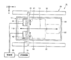
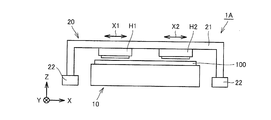
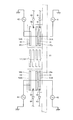
- FIG. 1 It is a schematic plan view of the pattern inspection apparatus in Embodiment 1 of this invention. It is a schematic side view of the pattern inspection apparatus shown in FIG. It is a schematic diagram which shows the structure of the inspection head shown in FIG. 1 and FIG. It is a schematic diagram which shows the outline of the pattern inspection method in Embodiment 1 of this invention.
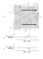
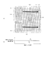
- the pattern inspection method in Embodiment 1 of this invention it is a figure which shows a mode that an open defect line is detected in the source line located in a large sized cell area
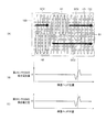
- the pattern inspection method in Embodiment 1 of this invention it is a figure which shows a mode that a short defect line is detected in the source line located in a large sized cell area
- the pattern inspection method in Embodiment 1 of this invention it is a figure which shows a mode that the cross short defect line with respect to a gate line is detected in the source line located in a large sized cell area
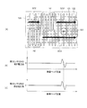
- the pattern inspection method in Embodiment 1 of this invention it is a figure which shows a mode that the cross short defect line with respect to a gate line is detected in the source line located in a small cell area
- the pattern inspection method in Embodiment 1 of this invention it is a figure which shows a mode that an open defect line is detected in the source line located in a small cell area
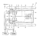
- FIG. 1 is a schematic plan view of a pattern inspection apparatus according to Embodiment 1 of the present invention
- FIG. 2 is a schematic side view of the pattern inspection apparatus shown in FIG.
- FIG. 3 is a schematic diagram showing the configuration of the inspection head shown in FIGS. 1 and 2.
- the pattern inspection apparatus 1A includes a stage 10 on which a common substrate 100 that is an inspection target substrate is placed, a first inspection head H1 that is a pair of inspection heads, and a second inspection head. And a gantry 20 to which H2 is attached.
- the gantry 20 includes an arm 21 that supports the first inspection head H1 and the second inspection head H2, and a pair of rails 22 that are installed at positions that sandwich the stage 10, and both ends of the arm 21 are a pair of rails. 22 is movably supported.
- a first sensor S1A and a second sensor S2A used for pattern inspection are provided on the lower surface of the first inspection head H1, and a first sensor used for pattern inspection is provided on the lower surface of the second inspection head H2.
- S1B and second sensor S2B are provided (see FIG. 3). The details of the first sensors S1A and S1B and the second sensors S2A and S2B will be described later.
- the pattern inspection apparatus 1A drives the gantry 20 to scan the first inspection head H1 and the second inspection head H2 attached to the gantry 20 on the stage 10, and the above-described first mechanism. It further includes a control unit 80 for driving and controlling the sensors S1A and S1B, the second sensors S2A and S2B, and the scanning mechanism.
- the stage 10 has a placement surface on which the common substrate 100 is placed on its upper surface, and is placed so that the placement surface is parallel to the XY plane shown in the drawing.
- the first inspection head H1 and the second inspection head H2 are each configured to be movable along the X-axis direction shown in the drawing by the scanning mechanism 70 described above, and thereby, in the X1 direction and the X2 direction shown in the drawing. Move each one.
- the arm 21 of the gantry 20 to which the first inspection head H1 and the second inspection head H2 are attached is configured to be movable along the Y-axis direction shown in the drawing by the scanning mechanism 70 described above. It moves in the Y1 direction shown in the figure.
- a specific scanning mechanism 70 for driving the arm 21, the first inspection head H1, and the second inspection head H2 a known drive mechanism such as a linear motor or a ball screw can be used.
- the distance between the first inspection head H1 and the common substrate 100 and the distance between the second inspection head H2 and the common substrate 100 along the Z-axis direction shown in the figure. Is provided at a predetermined distance.
- an elevating mechanism that includes an air pressure sensor, a laser sensor, or the like and moves the stage 10 up and down based on detection results of these sensors can be used.
- the first inspection head H1 and the second inspection head H2 are both separated from the main surface of the common substrate 100 by a predetermined distance on the main surface of the common substrate 100 placed on the stage 10. In this state, it is configured to be able to scan.
- the scanning along the Y-axis direction may be performed by driving the stage 10, and the adjustment in the Z-axis direction is driven by the gantry 20 or the first inspection head H1 and the second inspection head H2. You may do it.
- the common substrate 100 is a glass substrate before a cell region included in the common substrate 100 is cut out, and includes a large cell region 110 and a small cell region 120.
- the large cell region 110 has a first wiring pattern including a plurality of long first conductive lines arranged in parallel to each other, and the small cell region 120 has a length arranged in parallel to each other.
- a second wiring pattern including a plurality of second conductive lines of the scale is located.
- the first conductive lines located in the large cell region 110 include source lines 111 arranged in rows and gate lines 112 arranged in rows (see FIG. 5 and the like).
- the second conductive lines located in the line include source lines 121 arranged in a column and gate lines 122 arranged in a row (see FIG. 8 and the like).
- the first sensor S ⁇ b> 1 ⁇ / b> A is provided in the first inspection head H ⁇ b> 1 and has a relatively large area extending along the extending direction of the source line 111 to be inspected.
- the power supply electrode 31 is an electrode for applying an AC voltage in a non-contact manner near one end of the source line 111, and is connected to the AC power supply 41.
- the detection electrode 51 is an electrode for detecting the AC voltage induced at the one end of the source line 111 in a non-contact manner, and is connected to the amplifier 61.
- the first sensor S1B is provided in the second inspection head H2, and includes a plate-like power supply electrode 33 having a relatively large area extending along the extending direction of the source line 111 to be inspected, and the source line. And a flat detection electrode 53 having a relatively small area, which is disposed at the other end of 111.
- the power supply electrode 33 is an electrode for applying an AC voltage in a non-contact manner near the other end of the source line 111, and is connected to the AC power supply 43.
- the detection electrode 53 is an electrode for detecting the AC voltage induced at the other end of the source line 111 in a non-contact manner, and is connected to the amplifier 63.
- the first sensors S1A and S1B detect the defective line based on the AC voltage as the detection signal obtained from the one source line by applying the AC voltage as the inspection signal to the one source line.
- the signal amplified by the amplifiers 61 and 63 is processed by a signal processing unit provided in the control unit 80 or the like, so that a defective line is specified.
- these first sensors S 1 A and S 1 B are used only for detecting an open defect line included in the source line 111 located in the large cell region 110.
- the source lines 111 having no open defects are simultaneously applied. These reversed-phase AC voltages cancel each other, so that the noise component is effectively removed and the AC voltage applied to the detection electrodes 51 and 53 stably shows almost “0”.
- the source line 111 having an open defect cancellation of the AC voltages of opposite phases applied at the same time is hindered, so that the AC voltage applied to the detection electrodes 51 and 53 greatly fluctuates. . Therefore, if it does in this way, an open defect line can be detected with high sensitivity by these 1st sensors S1A and S1B working together.
- the second sensor S2A is provided in the first inspection head H1, and relatively extends along the extending direction of the source line adjacent to the source lines 111 and 121 to be inspected.
- a pair of plate-like power supply electrodes 32a and 32b having a large area and a plate-like detection electrode 52 having a relatively small area disposed at one end of the source lines 111 and 121 to be inspected are provided.
- the power feeding electrodes 32a and 32b are electrodes for applying an AC voltage in a non-contact manner in the vicinity of one end portion of the source line adjacent to the source lines 111 and 121 to be inspected, and are connected to the AC power source 42, respectively.
- the detection electrode 52 is an electrode for detecting the AC voltage induced at the one end of the source lines 111 and 121 to be inspected in a non-contact manner, and is connected to the amplifier 62.
- the second sensor S2B is provided in the second inspection head H2, and has a pair of flat plates having a relatively large area extending along the extending direction of the source line adjacent to the source lines 111 and 121 to be inspected.
- Power supply electrodes 34a and 34b, and a flat detection electrode 54 having a relatively small area disposed at the other end of the source lines 111 and 121 to be inspected.
- the feed electrodes 34 a and 34 b are electrodes for applying an AC voltage in a non-contact manner near the other end of the source line adjacent to the source lines 111 and 121 to be inspected, and are respectively connected to the AC power supply 44.
- the detection electrode 54 is an electrode for detecting the AC voltage induced at the other end of the source lines 111 and 121 to be inspected in a non-contact manner, and is connected to the amplifier 64.
- the second sensors S2A and S2B are based on the AC voltage as the detection signal obtained from the source line different from the one source line by applying the AC voltage as the inspection signal to the one source line. This is for detecting a defective line, and the signal amplified by the amplifiers 62 and 64 is processed by a signal processing unit provided in the control unit 80 or the like, whereby the defective line is specified.
- these second sensors S2A and S2B detect short defect lines (including detection of cross short defect lines) included in the source line 111 located in the large cell area 110, and small cell areas.
- 120 is used for detection of an open defect line included in the source line 121 located in 120 and detection of a short defect line (including detection of a cross short defect line which is a short defect with respect to the gate line 122).
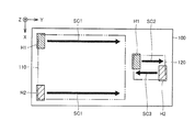
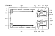
- FIG. 4 is a schematic diagram showing an outline of the pattern inspection method in the present embodiment.
- 5 to 7 are diagrams showing how various defect lines are detected in the source line located in the large cell region in the pattern inspection method according to the present embodiment.
- 8 to 10 are diagrams showing how various defect lines are detected in the source line located in the small cell region in the pattern inspection method according to the present embodiment.
- pattern inspection is performed by performing a total of three scans in this order as indicated by arrows SC1 to SC3 in the figure.
- the three scans are performed by moving the arm 21 of the gantry 20 to which the first inspection head H1 and the second inspection head H2 are attached along the Y-axis direction shown in the drawing.
- the first inspection head H1 and the second inspection head H2 are individually moved along the X-axis direction shown in the drawing as necessary.
- the first inspection head H1 and the second inspection head H2 are scanned on the large cell region 110 of the common substrate 100, they are simultaneously scanned in parallel.
- the first inspection head H1 and the second inspection head H2 are scanned on the small cell region 120 of the common substrate 100, these are individually scanned. This is because the feeding electrodes 31 and 33 are elongated along the extending direction of the source line 111 in order to increase the inspection accuracy when detecting an open defect line included in the source line 111 located in the large cell region 110.
- the first inspection head H1 and the second inspection head H2 are respectively increased in size, and the first inspection head H1 and the second inspection head H2 are detected when the defect line included in the source line 121 located in the small cell region 120 is detected. This is because the inspection head H2 comes into contact with physical interference and cannot be disposed on both ends of the source line 121.
- the first inspection head H1 and the first inspection head H1 are partially overlapped with each other in order to partially overlap the orbit of the first inspection head H1.
- the above-described physical interference does not occur by individually scanning so that the second inspection head H2 passes over each end of the source line 121 with a time difference.
- open defect lines included in the source line 121 located in the small cell region 120 cannot be detected by the first sensors S1A and S1B.
- This is performed by a pair of second sensors S2A and S2B provided in the first inspection head H1 and the second inspection head H2.
- the end of the large cell region 110 of the common substrate 100 in the direction orthogonal to the extending direction of the source line 111 and the extending of the source line 111 is used.
- the first inspection head H1 and the second inspection head H2 are arranged on both end portions along the existing direction, and the first inspection head H1 and the first inspection head H1 in the direction orthogonal to the extending direction of the source line 111 (that is, the Y-axis direction)
- the second inspection head H2 is scanned.
- the first inspection head H1 and the second inspection head H2 run side by side so that the first inspection head H1 and the second inspection head H2 simultaneously pass over the respective end portions of the source line 111. Scanned.
- the defect lines included in the source line 111 located in the large cell region 110 are the first sensors S1A and S1B provided in the first inspection head H1 and the second inspection head H2, and the first Two sensors S2A and S2B are specified. If sufficient detection accuracy is obtained even when only one of the second sensors S2A and S2B is used, only the second sensor S2A provided in the first inspection head H1 is used. The second sensor S2B provided in the second inspection head H2 may not be used.
- the end of the open defect line is When the first inspection head H1 and the second inspection head H2 pass through, as shown in FIGS. 5B and 5C, the detection electrodes 51 and 53 included in the first sensors S1A and S1B detect The AC voltage to be changed greatly, and this can be detected with a high S / N ratio (signal to noise ratio) by analyzing the waveform in the processing circuit unit described above. Thereby, an open defect line is specified.
- the S / N ratio at that time is about 150 although it depends on the length of the source line 111 and the lengths of the feeding electrodes 31 and 33.
- the source line 111 located in the large cell region 110 includes a short defect line including a short defect A2 (here, a short defect between the source lines 111).
- a short defect line including a short defect A2 (here, a short defect between the source lines 111).
- the AC voltage detected by the detection electrode 51 included in the second sensor S2A is It changes greatly, and it becomes possible to detect with a high S / N ratio by analyzing the waveform in the processing circuit unit described above. As a result, the short defect line is identified.
- the source line 111 located in the large cell region 110 includes a cross short defect line including a cross short defect A3 with respect to the gate line 112, for example.
- the AC voltage detected by the detection electrode 51 included in the second sensor S2A greatly changes as shown in FIG. 7B.
- this can be detected with a high S / N ratio by analyzing the waveform in the processing circuit unit described above.
- the cross short defect line is identified.
- FIG. 6 and FIG. 7 there is a difference in the way the waveform fluctuates between the case where there is a short defect and the case where there is a cross short defect, and these can be distinguished by the above waveform analysis. .
- the source line is an end in the direction perpendicular to the extending direction of the source line 121 of the small cell region 120 of the common substrate 100.
- the first inspection head H1 is disposed on one end portion along the extending direction of 121, and the first inspection head H1 is scanned in a direction orthogonal to the extending direction of the source line 121 (that is, the Y-axis direction). .
- the first inspection head H ⁇ b> 1 is scanned alone so that the first inspection head H ⁇ b> 1 passes over each one end portion of the source line 121.
- the second inspection head H2 is disposed on the other end along the extending direction of the source line 121, and the second inspection head H2 is directed in a direction orthogonal to the extending direction of the source line 121 (that is, the Y-axis direction). Scanned. At that time, the second inspection head H ⁇ b> 2 is scanned alone so that the second inspection head H ⁇ b> 2 passes over each other end of the source line 121.
- the defect lines included in the source line 121 located in the small cell region 120 are second sensors S2A provided in the first inspection head H1 and the second inspection head H2 described above. Specified by S2B.
- the first sensors S1A and S1B provided in the first inspection head H1 and the second inspection head H2 are not used here.
- the end of the open defect line is Are detected by the detection electrodes 51 and 53 included in the second sensors S2A and S2B, as shown in FIGS. 8B and 8C, when the first inspection head H1 and the second inspection head H2 pass. It is possible to detect with a high S / N ratio by analyzing the waveform in the above-described processing circuit unit. Thereby, an open defect line is specified.
- the S / N ratio at that time is approximately 15 to 30 although it depends on the length of the source line 121 and the lengths of the feed electrodes 31 and 33.
- the source line 121 located in the small cell region 120 includes a short defect line including the short defect B2 (here, a short defect between the source lines 121).
- the first inspection head H1 passes over one end portion of the short defect line, as shown in FIGS. 9B and 9C, it is detected by the detection electrode 51 included in the second sensor S2A. It is possible to detect with a high S / N ratio by analyzing the waveform in the processing circuit unit described above. As a result, the short defect line is identified.
- FIG. 8 and FIG. 9 there is no significant difference in the way the waveform swings when there is an open defect and when there is a short defect, and it is difficult to distinguish these by the above-described waveform analysis.
- the cross short defect line is identified.
- FIG. 8 to FIG. 10 there is a difference in the waveform fluctuation between the case where there is an open defect and a short defect, and the case where there is a cross short defect. Is possible.
- the operation of the mechanism 70 is realized by driving and controlling them by the control unit 80 described above.
- FIG. 11 is a diagram showing in more detail how the open defect line is detected in the source line located in the small cell region in the pattern inspection method according to the present embodiment.
- the first inspection head H1 and the second inspection head H2 are both portions near one end of the source line 121 located in the small cell region 120. Since it passes only above, if there is an open defect near the edge located on the opposite side of the edge, it can be detected by scanning only one of them. Becomes difficult.
- the first inspection head H1 and the second inspection head H2 pass over one end and the other end of the source line 121 with a time difference.
- an open defect line is detected with high sensitivity by at least one of the second sensors S2A and S2B provided in the first inspection head H1 and the second inspection head H2. Therefore, by comprehensively judging these detection results together, it is possible to detect an open defect at any position.
- the pattern inspection apparatus 1A and the pattern inspection method according to the present embodiment are used to perform the defect inspection of the source lines 111 and 121 included in the common substrate 100, so that the first inspection head H1 and It is possible to detect a defect pattern with high accuracy and simplicity while avoiding physical interference of the second inspection head H2.
- the non-contact type sensor having an approximate configuration is scanned by the first sensor or the second sensor described above along the extending direction of the defect line.
- a known method such as a method of specifying a defect position or a method of specifying a defect position using an image processing technique can be applied. If this technique is used, the distinction between open defect lines and short defect lines (here, excluding cross-short defect lines) in the small cell area detected according to the pattern inspection method in the present embodiment is used for pattern inspection by this technique. Will be able to do it.
- FIG. 12 is a schematic diagram showing an outline of a first modification of the pattern inspection method according to the present embodiment.
- pattern inspection is performed by performing a total of three scans in this order as indicated by arrows SC1 to SC3 in the figure. .
- the first and second scans are the same as those in the present embodiment described above, and the scan direction of the third scan is opposite. In this way, the first and second scans are performed on the forward path, and the third scan is performed on the return path, so that the effect of shortening the tact time can be obtained.
- FIG. 13 is a schematic diagram showing an outline of a second modification of the pattern inspection method in the present embodiment.
- two small cell regions 120 are formed on the common substrate 100, and a total of 5 as indicated by arrows SC1 to SC5 in the figure.
- the pattern inspection is performed by performing the scans in this order in this order.
- the two scans performed on the two small cell regions 120 are similar scans. As described above, if scanning is repeated a plurality of times, even if there are three or more cell regions on the double-sided substrate 100, this can be easily pattern-inspected.
- FIG. 14 is a schematic plan view of the pattern inspection apparatus according to the second embodiment of the present invention
- FIG. 15 is a schematic diagram showing an outline of the pattern inspection method according to the present embodiment.
- the gantry 20 provided in the pattern inspection apparatus 1B has a pair of sub-arms 23 in addition to the arms 21, and the first inspection head H1 and the second inspection head H2 are a pair of sub-arms.
- the pair of sub-arms 23 are attached to the arms 21.
- the first inspection head H1 and the second inspection head H2 are configured to be movable along the Y-axis direction shown in the drawing by the scanning mechanism 70, respectively, thereby moving in the Y2 direction and Y3 direction shown in the drawing, respectively.
- the pair of sub-arms 23 of the gantry 20 to which the first inspection head H1 and the second inspection head H2 are attached are configured to be movable along the X-axis direction shown in the drawing by the scanning mechanism 70 described above. Thereby, it moves in the X1 and X2 directions shown in the figure.
- the arm 21 of the gantry 20 to which the pair of sub-arms 23 is attached is configured to be movable along the Y-axis direction shown in the figure by the scanning mechanism 70, and thereby moves in the Y1 direction shown in the figure.
- a specific scanning mechanism 70 for driving the arm 21, the first inspection head H1, the second inspection head H2, and the pair of sub arms 23, for example, a known drive mechanism such as a linear motor or a ball screw can be used. is there.
- the positions of the first inspection head H1 and the second inspection head H2 are not only different along the X-axis direction but also different along the Y-axis direction. Therefore, the first inspection head H1 and the second inspection head H2 can be disposed so as to overlap along the Y-axis direction while avoiding physical interference.
- the second scan is performed by performing a total of two scans in this order as indicated by arrows SC1 and SC2.
- the first inspection head H1 and the second inspection head H2 can be scanned so as to pass over both end portions of the small cell region 120 with a time difference at the same time without scanning the first inspection head H1 and the second inspection head H2. Therefore, the third scan as in the first embodiment is not necessary, and the effect of shortening the tact time can be obtained.
- the open defect line and the short defect line included in the source line formed on the common substrate used in the manufacturing process of the liquid crystal panel.
- the present invention can also be applied to the case of inspecting a cross-short defect line with respect to a Cs line included in a source line formed on a common substrate.
- the present invention is not limited to pattern inspection of conductive lines formed on a common substrate used in a liquid crystal panel manufacturing process, but also on conductive lines formed on a common substrate used in a semiconductor memory manufacturing process. It can also be applied to pattern inspection and the like.
- 1A, 1B pattern inspection device 10 stage, 20 gantry, 21 arm, 22 rail, 23 sub arm, 31, 32a, 32b, 33, 34a, 34b feed electrode, 41-44 AC power supply, 51-54 detection electrode, 61- 64 amplifiers, 70 scanning mechanisms, 80 control units, 100 co-substrate, 110 large cell region, 111 source line, 112 gate line, 120 small cell region, 121 source line, 122 gate line, A1, B1 open defect, A2, B2 short defect, A3, B3 cross short defect, H1 first inspection head, H2 second inspection head, S1A, S1B first sensor, S2A, S2B second sensor.
Landscapes
- Physics & Mathematics (AREA)
- Engineering & Computer Science (AREA)
- General Physics & Mathematics (AREA)
- Computer Hardware Design (AREA)
- Theoretical Computer Science (AREA)
- Testing Of Short-Circuits, Discontinuities, Leakage, Or Incorrect Line Connections (AREA)
Abstract
大型セル領域(110)と小型セル領域(120)とを含む共取り基板(100)に設けられたソースラインに含まれるオープン欠陥ラインおよびショート欠陥ラインを、第1検査ヘッド(H1)および第2検査ヘッド(H2)を有するパターン検査装置を用いて検出する。その際、大型セル領域(110)上においては、第1検査ヘッド(H1)および第2検査ヘッド(H2)を並走して走査させつつ、パターン検査を行なう。また、小型セル領域(110)上においては、第1検査ヘッド(H1)の軌道と第2検査ヘッド(H2)の軌道とを一部重複させるべく、第1検査ヘッド(H1)および第2検査ヘッド(H2)を時間差をもって走査しつつ、パターン検査を行なう。
Description
本発明は、複数の導電ラインを含む配線パターンに含まれる欠陥ラインを検出するパターン検査方法およびパターン検査装置に関し、より特定的には、大型セル領域と小型セル領域とを含む検査対象基板に設けられた複数の導電ラインに含まれる欠陥ラインを検出するパターン検査方法およびパターン検査装置に関する。
液晶パネルや半導体メモリ等においては、互いに並行して配置された複数の導電ラインが行状および列状に基板上に積層形成される。たとえば、液晶パネルにあっては、ゲートラインやCsラインと呼ばれる導電ラインが複数行状に配置された層と、ソースラインと呼ばれる導電ラインが複数列状に配置された層とが、ガラス基板の主表面上に層間絶縁膜を介して積層形成される。
これら導電ラインは、所望の形状に精緻にパターニングされていることが必要である。しかしながら、これら導電ラインは、いずれもそのライン幅が非常に狭くかつ隣り合う導電ライン間の配置ピッチも非常に小さいため、製造時における何らかの不具合等により、形成された導電ラインのパターンに欠陥(すなわち形状異常)が生じてしまう場合がある。そのため、製造途中において、形成された導電ラインのパターンに欠陥がないかパターン検査が実施され、当該パターン検査において欠陥が生じている箇所が特定されることで適宜リペアが実施される。
なお、上記欠陥には、主として、導電ラインの一部に断線が生じてしまうオープン欠陥や、導電ライン間に短絡が生じてしまうショート欠陥(特に、層間絶縁膜を介して異種の導電ライン間が短絡してしまうものをクロスショート欠陥と称する場合がある)が含まれる。
上述したパターン検査方法が開示された文献としては、たとえば特開2008-102031号公報(特許文献1)や、特開2006-200994号公報(特許文献2)、特開2009-229467号公報(特許文献3)等がある。これら公報に開示のパターン検査方法は、いずれも導電ラインに離間して給電電極および検出電極を対向配置することでこれらの間に形成される静電結合を利用して非接触でパターン検査を行なうものであり、具体的には、給電電極から導電ラインに交流電圧を印加し、これによって導電ラインに誘起される交流電圧を検出電極を用いて検出し、得られた検出波形の波形解析を行なうことで導電ラインのパターン検査が実施される。
このうち、上記特開2008-102031号公報には、導電ラインの延在方向に沿って配置された1つの給電電極と1つの検出電極とからなるセンサを導電ラインの両端に一対配置し、それぞれの給電電極から印加される交流電圧の位相を180°異ならしめることにより、これら一対のセンサが共働することで感度よくオープン欠陥を含む導電ライン(以下、オープン欠陥ラインと称する)が検出できることが記載されている。
また、上記特開2008-102031号公報には、導電ラインの延在方向と交差する方向に沿って配置された2つの給電電極とその間に配置された1つの検出電極とからなるセンサを用いることにより、当該センサによって感度よくショート欠陥を含む導電ライン(以下、ショート欠陥ラインと称する)が検出できることが記載されている(なお、以下においては、クロスショート欠陥を含む導電ラインを特にクロスショート欠陥ラインと称する場合もある)。
さらには、上記特開2008-102031号公報には、上述した2種類のセンサをそれぞれ導電ラインの延在方向と交差する方向に走査させることにより、短時間で効率的にオープン欠陥ラインおよびショート欠陥ラインの検出ができることが記載されている。
ところで、近年においては、液晶パネルの生産効率の向上を図るとともにガラス基板の利用効率を高めるために、大型のガラス基板にサイズの異なるセル領域を複数配し、各種加工を行なった後に当該ガラス基板を裁断することでこれらセル領域を切り出して個々に液晶パネルのTFT(thin film transistor)基板として利用することが行なわれている。当該サイズの異なる複数のセル領域を含む基板は、一般に共取り基板と称され、当該共取り基板を用いた液晶パネルの生産工程にあっても、通常の基板(同サイズのセル領域のみを含む基板)を用いる場合と同様に、上述したガラス基板の裁断前にパターン検査が実施される必要がある。
一方で、近年においては、液晶パネルの大型化が飛躍的に進んでおり、そのため上述したゲートライン、Csラインおよびソースラインも長尺のものとなっている。そのため、パターン検査における検査精度を十分に維持するためには、上述したセンサに含まれる給電電極をこれら導電ラインの延在方向に沿って長尺化することが必要不可欠であり、その結果、上述したセンサが設けられる一対の検査ヘッドも必然的に大型化する傾向にある。
そのため、共取り基板を用いた生産工程におけるパターン検査工程において、大型セル領域内に位置する長尺の導電ラインにおける検査精度を高めるために一対の検査ヘッドを大型化した場合には、小型セル領域内に位置する短尺の導電ラインのパターン検査時において、一対の検査ヘッド同士が物理的に干渉することで接触してしまい、一対の検査ヘッドを短尺の導電ラインの両端部上に配置することができず、パターン検査が行なえない問題が生じてしまう。
これを解決するためには、異なる長さの導電ラインに対応して、一対の検査ヘッドをパターン検査装置に複数組具備させることが考えられるが、そのように構成した場合には、パターン検査装置の装置構成が非常に複雑化してしまう問題が生じてしまう。
したがって、本発明は、上述した問題を解決すべくなされたものであり、大型セル領域と小型セル領域とを含む検査対象基板に設けられた導電ラインに含まれる欠陥ラインを簡便に検出することができるパターン検査方法およびパターン検査装置を提供することを目的とする。
本発明に基づくパターン検査方法は、大型セル領域と小型セル領域とを含む検査対象基板に設けられた導電ラインに含まれるオープン欠陥ラインおよびショート欠陥ラインを第1検査ヘッドおよび第2検査ヘッドを有するパターン検査装置を用いて検出する方法である。上記大型セル領域には、互いに並行して配置された複数の長尺の第1導電ラインを含む第1配線パターンが位置しており、上記小型セル領域には、互いに並行して配置された複数の短尺の第2導電ラインを含む第2配線パターンが位置している。なお、ショート欠陥ラインには、隣り合う同種の導電ライン間に短絡が生じてしまう欠陥と、異種の導電ライン間が短絡してしまう欠陥とが含まれる。
上記パターン検査装置は、一の導電ラインに検査信号を印加することで当該一の導電ラインから得られる検出信号に基づいて欠陥ラインを検出する第1センサと、一の導電ラインに検査信号を印加することで当該一の導電ラインとは異なる他の導電ラインから得られる検出信号に基づいて欠陥ラインを検出する第2センサとを含んでいる。上記第1センサは、共働すべく上記第1検査ヘッドおよび上記第2検査ヘッドの双方に対を成して設けられており、上記第2センサは、上記第1検査ヘッドおよび上記第2検査ヘッドの双方に設けられている。
そして、上記本発明に基づくパターン検査方法は、以下のステップAおよびBを備えている。
A:上記大型セル領域上において、上記第1検査ヘッドおよび上記第2検査ヘッドが上記第1導電ラインの個々の端部上を同時に通過することとなるように、上記第1検査ヘッドおよび上記第2検査ヘッドを上記第1導電ラインの延在方向と交差する方向に沿って並走して走査しつつ、上記第1配線パターンに含まれるオープン欠陥ラインを上記第1センサにて検出するとともに、上記第1配線パターンに含まれるショート欠陥ラインを上記第2センサにて検出するステップ。
B:上記小型セル領域上において、上記第1検査ヘッドの軌道と上記第2検査ヘッドの軌道とを一部重複させるべく、上記第1検査ヘッドおよび上記第2検査ヘッドが上記第2導電ラインの個々の端部上を時間差をもって通過することとなるように、上記第1検査ヘッドおよび上記第2検査ヘッドを上記第2導電ラインの延在方向と交差する方向に沿って走査しつつ、上記第2配線パターンに含まれるオープン欠陥ラインおよびショート欠陥ラインをいずれも上記第2センサにて検出するステップ。
本発明に基づくパターン検査装置は、大型セル領域と小型セル領域とを含む検査対象基板に設けられた導電ラインに含まれるオープン欠陥ラインおよびショート欠陥ラインを検出するものでって、第1検査ヘッドと、第2検査ヘッドと、第1センサと、第2センサと、走査機構と、制御部とを備えている。上記大型セル領域には、互いに並行して配置された複数の長尺の第1導電ラインを含む第1配線パターンが位置しており、上記小型セル領域には、互いに並行して配置された複数の短尺の第2導電ラインを含む第2配線パターンが位置している。なお、ショート欠陥ラインには、隣り合う同種の導電ライン間に短絡が生じてしまう欠陥と、異種の導電ライン間が短絡してしまう欠陥とが含まれる。
上記第1検査ヘッドおよび上記第2検査ヘッドは、上記検査対象基板の主表面に対向配置されるものであり、上記走査機構は、上記検査対象基板の上記主表面上における上記第1検査ヘッドおよび上記第2検査ヘッドの位置を相対的に変化させることで上記第1検査ヘッドおよび上記第2検査ヘッドを走査させるものである。上記第1センサは、一の導電ラインに検査信号を印加することで当該一の導電ラインから得られる検出信号に基づいて欠陥ラインを検出するためのものであり、上記第2センサは、一の導電ラインに検査信号を印加することで当該一の導電ラインとは異なる他の導電ラインから得られる検出信号に基づいて欠陥ラインを検出するためのものである。上記第1センサは、共働すべく上記第1検査ヘッドおよび上記第2検査ヘッドの双方に対を成して設けられており、上記第2センサは、上記第1検査ヘッドおよび上記第2検査ヘッドの双方に設けられている。
そして、上記本発に基づくパターン検査装置にあっては、上記制御部が、上記大型セル領域上において、上記第1検査ヘッドおよび上記第2検査ヘッドが上記第1導電ラインの個々の端部上を同時に通過することとなるように、上記第1検査ヘッドおよび上記第2検査ヘッドを上記第1導電ラインの延在方向と交差する方向に沿って並走して走査させつつ、上記第1配線パターンに含まれるオープン欠陥ラインを上記第1センサにて検出するとともに、上記第1配線パターンに含まれるショート欠陥ラインを上記第2センサにて検出し、上記小型セル領域上において、上記第1検査ヘッドの軌道と上記第2検査ヘッドの軌道とを一部重複させるべく、上記第1検査ヘッドおよび上記第2検査ヘッドが上記第2導電ラインの個々の端部上を時間差をもって通過することとなるように、上記第1検査ヘッドおよび上記第2検査ヘッドを上記第2導電ラインの延在方向と交差する方向に沿って走査させつつ、上記第2配線パターンに含まれるオープン欠陥ラインおよびショート欠陥ラインをいずれも上記第2センサにて検出するように、上記第1センサ、上記第2センサおよび上記走査機構を駆動制御する。
本発明によれば、大型セル領域と小型セル領域とを含む検査対象基板に設けられた導電ラインに含まれる欠陥ラインを簡便に検出することができるパターン検査方法およびパターン検査装置とすることができる。
以下、本発明の実施の形態について、図を参照して詳細に説明する。以下に示す実施の形態1および2においては、液晶パネルの製造工程において使用される共取り基板に形成されたソースラインに含まれるオープン欠陥ラインおよびショート欠陥ライン(ゲートラインに対してのクロスショート欠陥ラインを含む)を検査するパターン検査方法およびパターン検査装置に本発明を適用した場合を例示して説明を行なう。なお、同一のまたは共通する部分には図中同一の符号を付し、その説明は繰り返さない。
(実施の形態1)
図1は、本発明の実施の形態1におけるパターン検査装置の概略平面図であり、図2は、図1に示すパターン検査装置の概略側面図である。また、図3は、図1および図2に示す検査ヘッドの構成を示す模式図である。まず、これら図1および図2を参照して、本発明の実施の形態1におけるパターン検査装置の構成について説明する。
図1は、本発明の実施の形態1におけるパターン検査装置の概略平面図であり、図2は、図1に示すパターン検査装置の概略側面図である。また、図3は、図1および図2に示す検査ヘッドの構成を示す模式図である。まず、これら図1および図2を参照して、本発明の実施の形態1におけるパターン検査装置の構成について説明する。
図1および図2に示すように、パターン検査装置1Aは、検査対象基板である共取り基板100が載置されるステージ10と、一対の検査ヘッドである第1検査ヘッドH1および第2検査ヘッドH2が取付けられたガントリ20とを備えている。ガントリ20は、第1検査ヘッドH1および第2検査ヘッドH2を支持するアーム21と、ステージ10を挟み込む位置に設置された一対のレール22とを含んでおり、当該アーム21の両端が一対のレール22に移動可能に支持されている。
第1検査ヘッドH1の下面には、パターン検査に使用される第1センサS1Aおよび第2センサS2Aが設けられており、第2検査ヘッドH2の下面には、パターン検査に使用される第1センサS1Bおよび第2センサS2Bが設けられている(図3参照)。なお、これら第1センサS1A,S1Bおよび第2センサS2A,S2Bの詳細については、後述することとする。
また、パターン検査装置1Aは、ガントリ20を駆動することでガントリ20に取付けられた第1検査ヘッドH1および第2検査ヘッドH2をステージ10上において走査させるための走査機構70と、上述した第1センサS1A,S1Bおよび第2センサS2A,S2Bならびに走査機構70を駆動制御する制御部80とをさらに備えている。
ステージ10は、共取り基板100が載置される載置面をその上面に有しており、当該載置面が図中に示すXY平面に平行となるように設置されている。
第1検査ヘッドH1および第2検査ヘッドH2は、それぞれ上述した走査機構70によって図中に示すX軸方向に沿って移動可能に構成されており、これにより図中に示すX1方向およびX2方向にそれぞれ移動する。また、第1検査ヘッドH1および第2検査ヘッドH2が取付けられたガントリ20のアーム21は、上述した走査機構70によって図中に示すY軸方向に沿って移動可能に構成されており、これにより図中に示すY1方向に移動する。なお、アーム21、第1検査ヘッドH1および第2検査ヘッドH2を駆動するための具体的な走査機構70としては、たとえばリニアモータやボールネジ等、公知の駆動機構が使用可能である。
また、パターン検査装置1Aには、図中に示すZ軸方向に沿って第1検査ヘッドH1と共取り基板100との間の距離および第2検査ヘッドH2と共取り基板100との間の距離を所定の距離に保つための機構が設けられている。当該機構としては、エア圧力センサやレーザセンサ等を含み、これらセンサの検出結果に基づいてステージ10を昇降させる昇降機構が使用可能である。
以上により、第1検査ヘッドH1および第2検査ヘッドH2は、いずれもステージ10上に載置された共取り基板100の主表面上において、当該共取り基板100の主表面と所定の距離だけ離間した状態で走査可能に構成されることになる。なお、Y軸方向に沿った走査は、ステージ10が駆動されることで行なってもよいし、Z軸方向の調整は、ガントリ20または第1検査ヘッドH1および第2検査ヘッドH2が駆動されることで行なってもよい。
共取り基板100は、当該共取り基板100に含まれるセル領域を切り出す前のガラス基板であり、大型セル領域110と、小型セル領域120とを有している。大型セル領域110には、互いに並行して配置された長尺の複数の第1導電ラインを含む第1配線パターンが位置しており、小型セル領域120には、互いに並行して配置された長尺の複数の第2導電ラインを含む第2配線パターンが位置している。上記大型セル領域110内に位置する第1導電ラインには、列状に配置されたソースライン111および行状に配置されたゲートライン112が含まれ(図5等参照)、上記小型セル領域120内に位置する第2導電ラインには、列状に配置されたソースライン121および行状に配置されたゲートライン122が含まれる(図8等参照)。
図3に示すように、第1センサS1Aは、第1検査ヘッドH1に設けられており、検査対象であるソースライン111の延在方向に沿って延びる比較的大きい面積を有する平板状の給電電極31と、当該ソースライン111の一端部に配置される比較的小さい面積を有する平板状の検出電極51とを有している。給電電極31は、ソースライン111の一端部近傍に非接触で交流電圧を印加するための電極であり、交流電源41に接続されている。検出電極51は、ソースライン111の上記一端部に誘起された交流電圧を非接触で検出するための電極であり、増幅器61に接続されている。
一方、第1センサS1Bは、第2検査ヘッドH2に設けられており、検査対象であるソースライン111の延在方向に沿って延びる比較的大きい面積を有する平板状の給電電極33と、ソースライン111の他端部に配置される比較的小さい面積を有する平板状の検出電極53とを有している。給電電極33は、ソースライン111の他端部近傍に非接触で交流電圧を印加するための電極であり、交流電源43に接続されている。検出電極53は、ソースライン111の上記他端部に誘起された交流電圧を非接触で検出するための電極であり、増幅器63に接続されている。
このように、第1センサS1A,S1Bは、一のソースラインに検査信号としての交流電圧を印加することで当該一のソースラインから得られる検出信号としての交流電圧に基づいて欠陥ラインを検出するためのものであり、増幅器61,63で増幅された信号を制御部80等に設けられた信号処理部において処理することで欠陥ラインが特定されることになる。本実施の形態においては、これら第1センサS1A,S1Bが、大型セル領域110内に位置するソースライン111に含まれるオープン欠陥ラインの検出にのみ使用される。
なお、第1センサS1A,S1Bに含まれる給電電極31,33のそれぞれから印加される交流電圧のレベルを同じとして位相を180°異ならしめることにより、オープン欠陥がないソースライン111においては、同時に印加されたこれら逆相の交流電圧が相互に打ち消しあうことになるため、ノイズ成分が有効に除去されて検出電極51,53に印加される交流電圧が安定的にほぼ「0」を示すことになり、オープン欠陥があるソースライン111においては、同時に印加されたこれら逆相の交流電圧の打ち消し合いが阻害されることになるため、検出電極51,53に印加される交流電圧が大きく振れることになる。したがって、このようにすれば、これら一対の第1センサS1A,S1Bが共働することで感度よくオープン欠陥ラインを検出することができる。
また、図3に示すように、第2センサS2Aは、第1検査ヘッドH1に設けられており、検査対象であるソースライン111,121に隣接するソースラインの延在方向に沿って延びる比較的大きい面積を有する一対の平板状の給電電極32a,32bと、検査対象であるソースライン111,121の一端部に配置される比較的小さい面積を有する平板状の検出電極52とを有している。給電電極32a,32bは、検査対象であるソースライン111,121に隣接するソースラインの一端部近傍に非接触で交流電圧を印加するための電極であり、それぞれ交流電源42に接続されている。検出電極52は、検査対象であるソースライン111,121の上記一端部に誘起された交流電圧を非接触で検出するための電極であり、増幅器62に接続されている。
一方、第2センサS2Bは、第2検査ヘッドH2に設けられており、検査対象であるソースライン111,121に隣接するソースラインの延在方向に沿って延びる比較的大きい面積を有する一対の平板状の給電電極34a,34bと、検査対象であるソースライン111,121の他端部に配置される比較的小さい面積を有する平板状の検出電極54とを有している。給電電極34a,34bは、検査対象であるソースライン111,121に隣接するソースラインの他端部近傍に非接触で交流電圧を印加するための電極であり、それぞれ交流電源44に接続されている。検出電極54は、検査対象であるソースライン111,121の上記他端部に誘起された交流電圧を非接触で検出するための電極であり、増幅器64に接続されている。
このように、第2センサS2A,S2Bは、一のソースラインに検査信号としての交流電圧を印加することで当該一のソースラインとは異なるソースラインから得られる検出信号としての交流電圧に基づいて欠陥ラインを検出するためのものであり、増幅器62,64で増幅された信号を制御部80等に設けられた信号処理部において処理することで欠陥ラインが特定されることになる。本実施の形態においては、これら第2センサS2A,S2Bが、大型セル領域110内に位置するソースライン111に含まれるショート欠陥ラインの検出(クロスショート欠陥ラインの検出を含む)と、小型セル領域120内に位置するソースライン121に含まれるオープン欠陥ラインの検出およびショート欠陥ラインの検出(ゲートライン122に対するショート欠陥であるクロスショート欠陥ラインの検出を含む)に使用される。
図4は、本実施の形態におけるパターン検査方法の概略を示す模式図である。図5ないし図7は、本実施の形態におけるパターン検査方法において、大型セル領域内に位置するソースラインにおいて各種欠陥ラインが検出される様子を示す図である。また、図8ないし図10は、本実施の形態におけるパターン検査方法において、小型セル領域内に位置するソースラインにおいて各種欠陥ラインが検出される様子を示す図である。以下においては、これら図4ないし図10を参照して、本実施の形態におけるパターン検査方法について説明する。
図4に示すように、本実施の形態におけるパターン検査方法においては、図中において矢印SC1~SC3で示す如くの合計3回の走査をこの順で行なうことにより、パターン検査が実施される。当該3回の走査は、いずれも第1検査ヘッドH1および第2検査ヘッドH2が取付けられたガントリ20のアーム21を図中に示すY軸方向に沿って移動させることで行ない、各回の走査の間には、必要に応じて第1検査ヘッドH1および第2検査ヘッドH2を図中に示すX軸方向に沿って個別に移動させる。
ここで、本実施の形態においては、共取り基板100の大型セル領域110上において第1検査ヘッドH1および第2検査ヘッドH2を走査させる際には、これらを同時に並走して走査させており、共取り基板100の小型セル領域120上において第1検査ヘッドH1および第2検査ヘッドH2を走査させる際には、これらを個別に走査させている。これは、大型セル領域110内に位置するソースライン111に含まれるオープン欠陥ラインの検出の際の検査精度を高めるために、給電電極31,33をソースライン111の延在方向に沿って長尺化した結果、第1検査ヘッドH1および第2検査ヘッドH2がそれぞれ大型化し、小型セル領域120内に位置するソースライン121に含まれる欠陥ラインの検出の際に、第1検査ヘッドH1および第2検査ヘッドH2が物理的に干渉することで接触してしまい、これらをソースライン121の両端部上に配置することができないためである。
しかしながら、本実施の形態の如く、共取り基板100の小型セル領域120上において、第1検査ヘッドH1の軌道および第2検査ヘッドH2の軌道とを一部重複させるべく、これら第1検査ヘッドH1および第2検査ヘッドH2がソースライン121の個々の端部上を時間差を持って通過することとなるように、個別に走査させることにより、上述した物理的な干渉が生じないことになる。その結果、小型セル領域120内に位置するソースライン121に含まれるオープン欠陥ラインの検出を第1センサS1A,S1Bで行なえないことになるが、本実施の形態におけるパターン検査方法にあっては、これを第1検査ヘッドH1および第2検査ヘッドH2に設けられた一対の第2センサS2A,S2Bで行なうこととしている。
図4ないし図7に示すように、1回目の走査においては、共取り基板100の大型セル領域110のソースライン111の延在方向と直交する方向における端部であってかつソースライン111の延在方向に沿った両端部上に第1検査ヘッドH1および第2検査ヘッドH2が配置され、ソースライン111の延在方向と直交する方向(すなわちY軸方向)に向けて第1検査ヘッドH1および第2検査ヘッドH2が走査される。その際、第1検査ヘッドH1および第2検査ヘッドH2がソースライン111の個々の端部上を同時に通過することとなるように、第1検査ヘッドH1および第2検査ヘッドH2が並走して走査される。
この1回目の走査においては、大型セル領域110内に位置するソースライン111に含まれる欠陥ラインが上述した第1検査ヘッドH1および第2検査ヘッドH2に設けられた第1センサS1A,S1Bおよび第2センサS2A,S2Bによって特定される。なお、第2センサS2A,S2Bのうち、一方のみを使用した場合にも十分な検出精度が得られる場合には、第1検査ヘッドH1に設けられた第2センサS2Aのみを使用することとし、第2検査ヘッドH2に設けられた第2センサS2Bは使用しないこととしてもよい。
具体的には、図5(A)に示すように、大型セル領域110内に位置するソースライン111にオープン欠陥A1を含むオープン欠陥ラインが含まれる場合には、当該オープン欠陥ラインの端部上を第1検査ヘッドH1および第2検査ヘッドH2が通過する際に、図5(B)および図5(C)に示すように、第1センサS1A,S1Bに含まれる検出電極51,53によって検出される交流電圧が大きく変化し、これを上述した処理回路部において波形解析することで高いS/N比(信号対ノイズ比)で検出することが可能となる。これにより、オープン欠陥ラインの特定が行なわれることになる。ここで、その際のS/N比は、ソースライン111の長さや給電電極31,33の長さにもよるが、概ね150程度である。
また、図6(A)に示すように、大型セル領域110内に位置するソースライン111にショート欠陥A2(ここでは、ソースライン111同士のショート欠陥)を含むショート欠陥ラインが含まれる場合には、たとえば、当該ショート欠陥ラインの一端部上を第1検査ヘッドH1が通過する際に、図6(B)に示すように、第2センサS2Aに含まれる検出電極51によって検出される交流電圧が大きく変化し、これを上述した処理回路部において波形解析することで高いS/N比で検出することが可能となる。これにより、ショート欠陥ラインの特定が行なわれることになる。
また、図7(A)に示すように、大型セル領域110内に位置するソースライン111にゲートライン112に対してのクロスショート欠陥A3を含むクロスショート欠陥ラインが含まれる場合には、たとえば、当該クロスショート欠陥ラインの一端部上を第1検査ヘッドH1が通過する際に、図7(B)に示すように、第2センサS2Aに含まれる検出電極51によって検出される交流電圧が大きく変化し、これを上述した処理回路部において波形解析することで高いS/N比で検出することが可能となる。これにより、クロスショート欠陥ラインの特定が行なわれることになる。ここで、図6および図7に示すように、ショート欠陥がある場合とクロスショート欠陥がある場合とでは、波形の振れ方に違いがあり、上記波形解析によってこれらを峻別することが可能である。
図4および図8ないし図10に示すように、2回目の走査においては、共取り基板100の小型セル領域120のソースライン121の延在方向と直交する方向における端部であってかつソースライン121の延在方向に沿った一端部上に第1検査ヘッドH1が配置され、ソースライン121の延在方向と直交する方向(すなわちY軸方向)に向けて第1検査ヘッドH1が走査される。その際、第1検査ヘッドH1がソースライン121の個々の一端部上を通過することとなるように、第1検査ヘッドH1が単独で走査される。
また、図4および図8ないし図10に示すように、3回目の走査においては、共取り基板100の小型セル領域120のソースライン121の延在方向と直交する方向における端部であってかつソースライン121の延在方向に沿った他端部上に第2検査ヘッドH2が配置され、ソースライン121の延在方向と直交する方向(すなわちY軸方向)に向けて第2検査ヘッドH2が走査される。その際、第2検査ヘッドH2がソースライン121の個々の他端部上を通過することとなるように、第2検査ヘッドH2が単独で走査される。
この2回目および3回目の走査においては、小型セル領域120内に位置するソースライン121に含まれる欠陥ラインが上述した第1検査ヘッドH1および第2検査ヘッドH2に設けられた第2センサS2A,S2Bによって特定される。なお、本実施の形態においては、第1検査ヘッドH1および第2検査ヘッドH2に設けられた第1センサS1A,S1Bは、ここでは使用しない。
具体的には、図8(A)に示すように、小型セル領域120内に位置するソースライン121にオープン欠陥B1を含むオープン欠陥ラインが含まれる場合には、当該オープン欠陥ラインの端部上を第1検査ヘッドH1および第2検査ヘッドH2が通過する際に、図8(B)および図8(C)に示すように、第2センサS2A,S2Bに含まれる検出電極51,53によって検出される交流電圧が大きく変化し、これを上述した処理回路部において波形解析することで高いS/N比で検出することが可能となる。これにより、オープン欠陥ラインの特定が行なわれることになる。ここで、その際のS/N比は、ソースライン121の長さや給電電極31,33の長さにもよるが、概ね15~30程度である。
また、図9(A)に示すように、小型セル領域120内に位置するソースライン121にショート欠陥B2(ここでは、ソースライン121同士のショート欠陥)を含むショート欠陥ラインが含まれる場合には、当該ショート欠陥ラインの一端部上を第1検査ヘッドH1が通過する際に、図9(B)および図9(C)に示すように、第2センサS2Aに含まれる検出電極51によって検出される交流電圧が大きく変化し、これを上述した処理回路部において波形解析することで高いS/N比で検出することが可能となる。これにより、ショート欠陥ラインの特定が行なわれることになる。ただし、図8および図9に示すように、オープン欠陥がある場合とショート欠陥がある場合とでは、波形の振れ方に大きな違いがなく、上記波形解析によってこれらを峻別することは困難である。
また、図10(A)に示すように、小型セル領域120内に位置するソースライン121にゲートライン122に対してのクロスショート欠陥B3を含むクロスショート欠陥ラインが含まれる場合には、当該クロスショート欠陥ラインの一端部上を第1検査ヘッドH1が通過する際に、図10(B)および図10(C)に示すように、第2センサS2Aに含まれる検出電極51によって検出される交流電圧が大きく変化し、これを上述した処理回路部において波形解析することで高いS/N比で検出することが可能となる。これにより、クロスショート欠陥ラインの特定が行なわれることになる。ここで、図8ないし図10に示すように、オープン欠陥およびショート欠陥がある場合とクロスショート欠陥がある場合とでは、波形の振れ方に違いがあり、上記波形解析によってこれらを峻別することが可能である。
なお、第1検査ヘッドH1および第2検査ヘッドH2の上述した如くの検出動作や、これら第1検査ヘッドH1および第2検査ヘッドH2を共取り基板100上において上述した如くに走査させるための走査機構70の動作は、いずれも上述した制御部80によってこれらが駆動制御されることで実現される。
また、図11は、本実施の形態におけるパターン検査方法において、小型セル領域内に位置するソースラインにおいてオープン欠陥ラインが検出される様子をより詳細に示す図である。上述したように、本実施の形態におけるパターン検査方法においては、第1検査ヘッドH1および第2検査ヘッドH2が、いずれも小型セル領域120内に位置するソースライン121の片側の端部寄りの部分上のみを通過することになるため、当該端部とは反対側に位置する端部の近傍にオープン欠陥が存在している場合には、これらのいずれか単独のみを走査させただけではその検出が困難になる。
しかしながら、本実施の形態におけるパターン検査方法においては、第1検査ヘッドH1および第2検査ヘッドH2が時間差をもってソースライン121の一端部上および他端部上を通過することになるため、図11(A)ないし図11(C)に示すように、少なくとも第1検査ヘッドH1および第2検査ヘッドH2に設けられた第2センサS2A,S2Bのいずれかによって感度よくオープン欠陥ラインが検出されることになるため、これらの検出結果をあわせて総合判断することにより、どのような位置にあるオープン欠陥であってもこれが検出できることになる。
以上において説明したように、本実施の形態におけるパターン検査装置1Aおよびパターン検査方法を採用して共取り基板100に含まれるソースライン111,121の欠陥検査を行なうことにより、第1検査ヘッドH1および第2検査ヘッドH2の物理的干渉を回避しつつ高精度にかつ簡便に欠陥パターンを検出することが可能になる。
なお、実際のパターン検査工程においては、上述した欠陥ラインを特定するパターン検査が実施された後に、当該欠陥ラインのどの位置に欠陥があるのかを特定するパターン検査がさらに実施されることになる。このパターン検査については、その詳細な説明はここでは省略するが、欠陥ラインの延在方向に沿って上述した第1センサまたは第2センサに近似の構成の非接触式センサを走査させることで電気的に欠陥位置を特定する手法や、画像処理技術を用いて欠陥位置を特定する手法等、公知の手法が適用できる。当該手法を利用すれば、本実施の形態におけるパターン検査方法に従って検出された小型セル領域におけるオープン欠陥ラインおよびショート欠陥ライン(ここでは、クロスショート欠陥ラインを除く)の峻別が、当該手法によるパターン検査において行なえることになる。
図12は、本実施の形態におけるパターン検査方法の第1変形例の概略を示す模式図である。図12に示すように、本第1変形例に係るパターン検査方法においては、図中において矢印SC1~SC3で示す如くの合計3回の走査をこの順で行なうことにより、パターン検査が実施される。当該3回の走査のうち、1回目および2回目の走査は、上述した本実施の形態におけるそれと同様であり、3回目の走査は、その走査方向が反対向きである。このようにすれば、往路において1回目および2回目の走査が行なわれ、復路において3回目の走査が行なわれることになり、タクトタイムを短縮できる効果が得られる。
図13は、本実施の形態におけるパターン検査方法の第2変形例の概略を示す模式図である。図13に示すように、本第2変形例に係るパターン検査方法においては、共取り基板100に2つの小型セル領域120が形成されており、図中において矢印SC1~SC5で示す如くの合計5回の走査をこの順で行なうことにより、パターン検査が実施される。このうち、2つの小型セル領域120上において実施されるそれぞれ2回の走査は、同様の走査である。このように、複数回走査を繰り返すこととすれば、共取り基板100に3つ以上のセル領域がある場合にも、これを簡便にパターン検査することができる。
(実施の形態2)
図14は、本発明の実施の形態2におけるパターン検査装置の概略平面図であり、図15は、本実施の形態におけるパターン検査方法の概略を示す模式図である。次に、これら図14および図15を参照して、本発明の実施の形態2におけるパターン検査装置の構成およびパターン検査方法について説明する。
図14は、本発明の実施の形態2におけるパターン検査装置の概略平面図であり、図15は、本実施の形態におけるパターン検査方法の概略を示す模式図である。次に、これら図14および図15を参照して、本発明の実施の形態2におけるパターン検査装置の構成およびパターン検査方法について説明する。
図14に示すように、パターン検査装置1Bに設けられたガントリ20は、アーム21に加え、一対のサブアーム23を有しており、第1検査ヘッドH1および第2検査ヘッドH2は、一対のサブアーム23に個別に取付けられており、一対のサブアーム23は、アーム21に取付けられている。
第1検査ヘッドH1および第2検査ヘッドH2は、それぞれ走査機構70によって図中に示すY軸方向に沿って移動可能に構成されており、これにより図中に示すY2方向およびY3方向にそれぞれ移動する。また、第1検査ヘッドH1および第2検査ヘッドH2が取付けられたガントリ20の一対のサブアーム23は、上述した走査機構70によって図中に示すX軸方向に沿って移動可能に構成されており、これにより図中に示すX1およびX2方向にそれぞれ移動する。さらに、一対のサブアーム23が取付けられたガントリ20のアーム21は、走査機構70によって図中に示すY軸方向に沿って移動可能に構成されており、これにより図中に示すY1方向に移動する。なお、アーム21、第1検査ヘッドH1、第2検査ヘッドH2および一対のサブアーム23を駆動するための具体的な走査機構70としては、たとえばリニアモータやボールネジ等、公知の駆動機構が使用可能である。
このように構成することにより、図14において破線で示すように、第1検査ヘッドH1および第2検査ヘッドH2の位置をX軸方向に沿って異ならしめるのみならずY軸方向に沿っても異ならしめることができるため、これら第1検査ヘッドH1および第2検査ヘッドH2を物理的干渉を避けつつY軸方向に沿って重なるように配置することが可能になる。
したがって、図15に示すように、本実施の形態におけるパターン検査方法にあっては、図中において矢印SC1,SC2で示す如くの合計2回の走査をこの順で行なうことにより、2回目の走査において、第1検査ヘッドH1と第2検査ヘッドH2とを個別に走査させることなく、1度の走査で同時に時間差をもって小型セル領域120の両端部上を通過するように走査させることが可能になるため、上述した実施の形態1の如くの3回目の走査が不要になり、タクトタイムを短縮できる効果が得られる。
以上において説明した本発明の実施の形態1および2においては、液晶パネルの製造工程において使用される共取り基板に形成されたソースラインに含まれるオープン欠陥ラインおよびショート欠陥ライン(ゲートラインに対してのクロスショート欠陥ラインを含む)を検査する場合を例示して説明を行なったが、当然に共取り基板に形成されたゲートラインおよびCsラインに含まれるオープン欠陥ラインおよびショート欠陥ラインを検査する場合や、共取り基板に形成されたソースラインに含まれるCsラインに対してのクロスショート欠陥ラインを検査する場合等にも本発明を適用することができる。
また、本発明は、液晶パネルの製造工程において使用される共取り基板に形成された導電ラインのパターン検査のみならず、半導体メモリの製造工程において使用される共取り基板に形成された導電ラインのパターン検査等にも適用することができる。
このように、今回開示した上記実施の形態はすべての点で例示であって、制限的なものではない。本発明の技術的範囲は請求の範囲によって画定され、また請求の範囲の記載と均等の意味および範囲内でのすべての変更を含むものである。
1A,1B パターン検査装置、10 ステージ、20 ガントリ、21 アーム、22 レール、23 サブアーム、31,32a,32b,33,34a,34b 給電電極、41~44 交流電源、51~54 検出電極、61~64 増幅器、70 走査機構、80 制御部、100 共取り基板、110 大型セル領域、111 ソースライン、112 ゲートライン、120 小型セル領域、121 ソースライン、122 ゲートライン、A1,B1 オープン欠陥、A2,B2 ショート欠陥、A3,B3 クロスショート欠陥、H1 第1検査ヘッド、H2 第2検査ヘッド、S1A,S1B 第1センサ、S2A,S2B 第2センサ。
Claims (2)
- 検査対象基板(100)に設けられた大型セル領域(110)内に位置する互いに並行して配置された複数の長尺の第1導電ライン(111)を含む第1配線パターンと、前記検査対象基板(100)に設けられた小型セル領域(120)内に位置する互いに並行して配置された複数の短尺の第2導電ライン(121)を含む第2配線パターンと、に含まれるオープン欠陥ラインおよびショート欠陥ラインを、第1検査ヘッド(H1)および第2検査ヘッド(H2)を有するパターン検査装置を用いて検出する、パターン検査方法であって、
前記パターン検査装置は、一の導電ラインに検査信号を印加することで当該一の導電ラインから得られる検出信号に基づいて欠陥ラインを検出する第1センサ(S1A,S1B)と、一の導電ラインに検査信号を印加することで当該一の導電ラインとは異なる他の導電ラインから得られる検出信号に基づいて欠陥ラインを検出する第2センサ(S2A,S2B)とを含み、
前記第1センサ(S1A,S1B)は、共働すべく前記第1検査ヘッド(H1)および前記第2検査ヘッド(H2)の双方に対を成して設けられ、
前記第2センサ(S2A,S2B)は、前記第1検査ヘッド(H1)および前記第2検査ヘッド(H2)の双方に設けられ、
前記大型セル領域(110)上において、前記第1検査ヘッド(H1)および前記第2検査ヘッド(H2)が前記第1導電ライン(111)の個々の端部上を同時に通過することとなるように、前記第1検査ヘッド(H1)および前記第2検査ヘッド(H2)を前記第1導電ライン(111)の延在方向と交差する方向に沿って並走して走査しつつ、前記第1配線パターンに含まれるオープン欠陥ラインを前記第1センサ(S1A,S1B)にて検出するとともに、前記第1配線パターンに含まれるショート欠陥ラインを前記第2センサ(S2A,S2B)にて検出するステップと、
前記小型セル領域(120)上において、前記第1検査ヘッド(H1)の軌道と前記第2検査ヘッド(H2)の軌道とを一部重複させるべく、前記第1検査ヘッド(H1)および前記第2検査ヘッド(H2)が前記第2導電ライン(121)の個々の端部上を時間差をもって通過することとなるように、前記第1検査ヘッド(H1)および前記第2検査ヘッド(H2)を前記第2導電ライン(121)の延在方向と交差する方向に沿って走査しつつ、前記第2配線パターンに含まれるオープン欠陥ラインおよびショート欠陥ラインをいずれも前記第2センサ(S2A,S2B)にて検出するステップとを備えた、パターン検査方法。 - 検査対象基板(100)に設けられた大型セル領域(110)内に位置する互いに並行して配置された複数の長尺の第1導電ライン(111)を含む第1配線パターンと、前記検査対象基板(100)に設けられた小型セル領域(120)内に位置する互いに並行して配置された複数の短尺の第2導電ライン(121)を含む第2配線パターンと、に含まれるオープン欠陥ラインおよびショート欠陥ラインを検出する、パターン検査装置であって、
前記検査対象基板(100)の主表面に対向配置される第1検査ヘッド(H1)および第2検査ヘッド(H2)と、
共働すべく前記第1検査ヘッド(H1)および前記第2検査ヘッド(H2)の双方に対を成して設けられ、一の導電ラインに検査信号を印加することで当該一の導電ラインから得られる検出信号に基づいて欠陥ラインを検出するための第1センサ(S1A,S1B)と、
前記第1検査ヘッド(H1)および前記第2検査ヘッド(H2)の双方に設けられ、一の導電ラインに検査信号を印加することで当該一の導電ラインとは異なる他の導電ラインから得られる検出信号に基づいて欠陥ラインを検出するための第2センサ(S2A,S2B)と、
前記検査対象基板(100)の前記主表面上における前記第1検査ヘッド(H1)および前記第2検査ヘッド(H2)の位置を相対的に変化させることで前記第1検査ヘッド(H1)および前記第2検査ヘッド(H2)を走査させる走査機構(70)と、
前記第1センサ(S1A,S1B)および前記第2センサ(S2A,S2B)を駆動制御するとともに、前記走査機構(70)を駆動制御する制御部(80)とを備え、
前記制御部(80)は、前記大型セル領域(110)上において、前記第1検査ヘッド(H1)および前記第2検査ヘッド(H2)が前記第1導電ライン(111)の個々の端部上を同時に通過することとなるように、前記第1検査ヘッド(H1)および前記第2検査ヘッド(H2)を前記第1導電ライン(111)の延在方向と交差する方向に沿って並走して走査させつつ、前記第1配線パターンに含まれるオープン欠陥ラインを前記第1センサ(S1A,S1B)にて検出するとともに、前記第1配線パターンに含まれるショート欠陥ラインを前記第2センサ(S2A,S2B)にて検出し、前記小型セル領域(120)上において、前記第1検査ヘッド(H1)の軌道と前記第2検査ヘッド(H2)の軌道とを一部重複させるべく、前記第1検査ヘッド(H1)および前記第2検査ヘッド(H2)が前記第2導電ライン(121)の個々の端部上を時間差をもって通過することとなるように、前記第1検査ヘッド(H1)および前記第2検査ヘッド(H2)を前記第2導電ライン(121)の延在方向と交差する方向に沿って走査させつつ、前記第2配線パターンに含まれるオープン欠陥ラインおよびショート欠陥ラインをいずれも前記第2センサ(S2A,S2B)にて検出するように、前記第1センサ(S1A,S1B)、前記第2センサ(S2A,S2B)および前記走査機構(70)を駆動制御する、パターン検査装置。
Applications Claiming Priority (2)
| Application Number | Priority Date | Filing Date | Title |
|---|---|---|---|
| JP2011-129126 | 2011-06-09 | ||
| JP2011129126 | 2011-06-09 |
Publications (1)
| Publication Number | Publication Date |
|---|---|
| WO2012169458A1 true WO2012169458A1 (ja) | 2012-12-13 |
Family
ID=47296021
Family Applications (1)
| Application Number | Title | Priority Date | Filing Date |
|---|---|---|---|
| PCT/JP2012/064365 Ceased WO2012169458A1 (ja) | 2011-06-09 | 2012-06-04 | パターン検査方法およびパターン検査装置 |
Country Status (1)
| Country | Link |
|---|---|
| WO (1) | WO2012169458A1 (ja) |
Citations (5)
| Publication number | Priority date | Publication date | Assignee | Title |
|---|---|---|---|---|
| JPH10107289A (ja) * | 1996-09-26 | 1998-04-24 | Matsushita Electric Ind Co Ltd | 液晶表示装置用アレイチップの製造方法 |
| JP2005241614A (ja) * | 2004-01-30 | 2005-09-08 | Nidec-Read Corp | 基板検査装置及び基板検査方法 |
| JP2006200994A (ja) * | 2005-01-19 | 2006-08-03 | Oht Inc | 検査装置及び検査方法並びに検査装置用センサ |
| JP2008102031A (ja) * | 2006-10-19 | 2008-05-01 | Tokyo Cathode Laboratory Co Ltd | パターン検査装置 |
| JP2009229467A (ja) * | 2009-04-17 | 2009-10-08 | Oht Inc | 回路パターン検査装置 |
-
2012
- 2012-06-04 WO PCT/JP2012/064365 patent/WO2012169458A1/ja not_active Ceased
Patent Citations (5)
| Publication number | Priority date | Publication date | Assignee | Title |
|---|---|---|---|---|
| JPH10107289A (ja) * | 1996-09-26 | 1998-04-24 | Matsushita Electric Ind Co Ltd | 液晶表示装置用アレイチップの製造方法 |
| JP2005241614A (ja) * | 2004-01-30 | 2005-09-08 | Nidec-Read Corp | 基板検査装置及び基板検査方法 |
| JP2006200994A (ja) * | 2005-01-19 | 2006-08-03 | Oht Inc | 検査装置及び検査方法並びに検査装置用センサ |
| JP2008102031A (ja) * | 2006-10-19 | 2008-05-01 | Tokyo Cathode Laboratory Co Ltd | パターン検査装置 |
| JP2009229467A (ja) * | 2009-04-17 | 2009-10-08 | Oht Inc | 回路パターン検査装置 |
Similar Documents
| Publication | Publication Date | Title |
|---|---|---|
| KR100883994B1 (ko) | 패턴 검사장치 | |
| JP5688421B2 (ja) | 表示パネルの検査方法 | |
| TWI417822B (zh) | 面板基板搬送裝置及顯示面板模組組裝裝置 | |
| JP2007206641A (ja) | リペア装置及びリペア方法 | |
| JP2012094770A (ja) | 検査装置および基板の位置決め方法 | |
| US9863991B2 (en) | Inspection device | |
| JP5305111B2 (ja) | 回路パターン検査装置 | |
| JP5352066B2 (ja) | 電子回路基板の製造装置 | |
| KR100832140B1 (ko) | 표시용 기판의 검사에 이용하는 센서 기판 및 이를 이용한표시용 기판의 검사 방법 | |
| TW201543044A (zh) | 定位裝置以及處理裝置 | |
| WO2012169458A1 (ja) | パターン検査方法およびパターン検査装置 | |
| JP4654829B2 (ja) | 部品実装状態検査装置及び方法 | |
| JPWO2011155044A1 (ja) | Tftアレイ検査の電子線走査方法およびtftアレイ検査装置 | |
| JP4835317B2 (ja) | プリント配線板の電気検査方法 | |
| KR20090028347A (ko) | 기판 리페어 장치 및 기판 검사/리페어 장치 | |
| KR101144769B1 (ko) | 스크린 프린팅 시스템 | |
| JP5418983B2 (ja) | 矩形板状物の割れ検査方法及び検査装置 | |
| JP5291665B2 (ja) | パネル処理システム及びパネル処理方法 | |
| KR100902246B1 (ko) | 유기발광 표시장치의 원장단위 검사 장치 | |
| JP5007925B2 (ja) | Tftアレイ検査における電子線走査方法 | |
| JP2012078127A (ja) | Tftアレイ検査装置およびtftアレイ検査方法 | |
| JP2012182273A (ja) | ガラス基板インライン検査方法及びその装置 | |
| JP5197249B2 (ja) | 液晶パネル検査装置及び液晶パネル検査方法 | |
| KR20010077695A (ko) | 정전용량 근접센서 프로브를 이용한 스캔방식의 검사장치및 방법 | |
| KR102886566B1 (ko) | 잉크젯 프린팅 시스템 |
Legal Events
| Date | Code | Title | Description |
|---|---|---|---|
| 121 | Ep: the epo has been informed by wipo that ep was designated in this application |
Ref document number: 12796149 Country of ref document: EP Kind code of ref document: A1 |
|
| NENP | Non-entry into the national phase |
Ref country code: DE |
|
| 122 | Ep: pct application non-entry in european phase |
Ref document number: 12796149 Country of ref document: EP Kind code of ref document: A1 |
|
| NENP | Non-entry into the national phase |
Ref country code: JP |