WO2012169208A1 - 半導体基板の製造方法および半導体基板 - Google Patents
半導体基板の製造方法および半導体基板 Download PDFInfo
- Publication number
- WO2012169208A1 WO2012169208A1 PCT/JP2012/003768 JP2012003768W WO2012169208A1 WO 2012169208 A1 WO2012169208 A1 WO 2012169208A1 JP 2012003768 W JP2012003768 W JP 2012003768W WO 2012169208 A1 WO2012169208 A1 WO 2012169208A1
- Authority
- WO
- WIPO (PCT)
- Prior art keywords
- compound semiconductor
- substrate
- layer
- semiconductor layer
- insulating layer
- Prior art date
- Legal status (The legal status is an assumption and is not a legal conclusion. Google has not performed a legal analysis and makes no representation as to the accuracy of the status listed.)
- Ceased
Links
Images







Classifications
-
- H—ELECTRICITY
- H10—SEMICONDUCTOR DEVICES; ELECTRIC SOLID-STATE DEVICES NOT OTHERWISE PROVIDED FOR
- H10P—GENERIC PROCESSES OR APPARATUS FOR THE MANUFACTURE OR TREATMENT OF DEVICES COVERED BY CLASS H10
- H10P70/00—Cleaning of wafers, substrates or parts of devices
- H10P70/20—Cleaning during device manufacture
- H10P70/23—Cleaning during device manufacture during, before or after processing of insulating materials
-
- H—ELECTRICITY
- H10—SEMICONDUCTOR DEVICES; ELECTRIC SOLID-STATE DEVICES NOT OTHERWISE PROVIDED FOR
- H10P—GENERIC PROCESSES OR APPARATUS FOR THE MANUFACTURE OR TREATMENT OF DEVICES COVERED BY CLASS H10
- H10P14/00—Formation of materials, e.g. in the shape of layers or pillars
- H10P14/20—Formation of materials, e.g. in the shape of layers or pillars of semiconductor materials
-
- H—ELECTRICITY
- H10—SEMICONDUCTOR DEVICES; ELECTRIC SOLID-STATE DEVICES NOT OTHERWISE PROVIDED FOR
- H10D—INORGANIC ELECTRIC SEMICONDUCTOR DEVICES
- H10D62/00—Semiconductor bodies, or regions thereof, of devices having potential barriers
- H10D62/80—Semiconductor bodies, or regions thereof, of devices having potential barriers characterised by the materials
- H10D62/85—Semiconductor bodies, or regions thereof, of devices having potential barriers characterised by the materials being Group III-V materials, e.g. GaAs
-
- H—ELECTRICITY
- H10—SEMICONDUCTOR DEVICES; ELECTRIC SOLID-STATE DEVICES NOT OTHERWISE PROVIDED FOR
- H10D—INORGANIC ELECTRIC SEMICONDUCTOR DEVICES
- H10D30/00—Field-effect transistors [FET]
- H10D30/01—Manufacture or treatment
- H10D30/021—Manufacture or treatment of FETs having insulated gates [IGFET]
-
- H—ELECTRICITY
- H10—SEMICONDUCTOR DEVICES; ELECTRIC SOLID-STATE DEVICES NOT OTHERWISE PROVIDED FOR
- H10D—INORGANIC ELECTRIC SEMICONDUCTOR DEVICES
- H10D30/00—Field-effect transistors [FET]
- H10D30/60—Insulated-gate field-effect transistors [IGFET]
-
- H—ELECTRICITY
- H10—SEMICONDUCTOR DEVICES; ELECTRIC SOLID-STATE DEVICES NOT OTHERWISE PROVIDED FOR
- H10D—INORGANIC ELECTRIC SEMICONDUCTOR DEVICES
- H10D64/00—Electrodes of devices having potential barriers
- H10D64/01—Manufacture or treatment
- H10D64/013—Manufacture or treatment of electrodes having a conductor capacitively coupled to a semiconductor by an insulator
- H10D64/01358—Manufacture or treatment of electrodes having a conductor capacitively coupled to a semiconductor by an insulator the insulator being formed after the semiconductor body, the semiconductor being a Group III-V material
-
- H—ELECTRICITY
- H10—SEMICONDUCTOR DEVICES; ELECTRIC SOLID-STATE DEVICES NOT OTHERWISE PROVIDED FOR
- H10D—INORGANIC ELECTRIC SEMICONDUCTOR DEVICES
- H10D64/00—Electrodes of devices having potential barriers
- H10D64/60—Electrodes characterised by their materials
- H10D64/66—Electrodes having a conductor capacitively coupled to a semiconductor by an insulator, e.g. MIS electrodes
- H10D64/68—Electrodes having a conductor capacitively coupled to a semiconductor by an insulator, e.g. MIS electrodes characterised by the insulator, e.g. by the gate insulator
- H10D64/691—Electrodes having a conductor capacitively coupled to a semiconductor by an insulator, e.g. MIS electrodes characterised by the insulator, e.g. by the gate insulator comprising metallic compounds, e.g. metal oxides or metal silicates
-
- H—ELECTRICITY
- H10—SEMICONDUCTOR DEVICES; ELECTRIC SOLID-STATE DEVICES NOT OTHERWISE PROVIDED FOR
- H10P—GENERIC PROCESSES OR APPARATUS FOR THE MANUFACTURE OR TREATMENT OF DEVICES COVERED BY CLASS H10
- H10P10/00—Bonding of wafers, substrates or parts of devices
-
- H—ELECTRICITY
- H10—SEMICONDUCTOR DEVICES; ELECTRIC SOLID-STATE DEVICES NOT OTHERWISE PROVIDED FOR
- H10P—GENERIC PROCESSES OR APPARATUS FOR THE MANUFACTURE OR TREATMENT OF DEVICES COVERED BY CLASS H10
- H10P14/00—Formation of materials, e.g. in the shape of layers or pillars
- H10P14/20—Formation of materials, e.g. in the shape of layers or pillars of semiconductor materials
- H10P14/34—Deposited materials, e.g. layers
- H10P14/3402—Deposited materials, e.g. layers characterised by the chemical composition
- H10P14/3414—Deposited materials, e.g. layers characterised by the chemical composition being group IIIA-VIA materials
- H10P14/3421—Arsenides
-
- H—ELECTRICITY
- H10—SEMICONDUCTOR DEVICES; ELECTRIC SOLID-STATE DEVICES NOT OTHERWISE PROVIDED FOR
- H10P—GENERIC PROCESSES OR APPARATUS FOR THE MANUFACTURE OR TREATMENT OF DEVICES COVERED BY CLASS H10
- H10P14/00—Formation of materials, e.g. in the shape of layers or pillars
- H10P14/60—Formation of materials, e.g. in the shape of layers or pillars of insulating materials
- H10P14/69—Inorganic materials
- H10P14/692—Inorganic materials composed of oxides, glassy oxides or oxide-based glasses
- H10P14/6938—Inorganic materials composed of oxides, glassy oxides or oxide-based glasses the material containing at least one metal element, e.g. metal oxides, metal oxynitrides or metal oxycarbides
- H10P14/6939—Inorganic materials composed of oxides, glassy oxides or oxide-based glasses the material containing at least one metal element, e.g. metal oxides, metal oxynitrides or metal oxycarbides characterised by the metal
- H10P14/69391—Inorganic materials composed of oxides, glassy oxides or oxide-based glasses the material containing at least one metal element, e.g. metal oxides, metal oxynitrides or metal oxycarbides characterised by the metal the material containing aluminium, e.g. Al2O3
-
- H—ELECTRICITY
- H10—SEMICONDUCTOR DEVICES; ELECTRIC SOLID-STATE DEVICES NOT OTHERWISE PROVIDED FOR
- H10D—INORGANIC ELECTRIC SEMICONDUCTOR DEVICES
- H10D62/00—Semiconductor bodies, or regions thereof, of devices having potential barriers
- H10D62/80—Semiconductor bodies, or regions thereof, of devices having potential barriers characterised by the materials
- H10D62/85—Semiconductor bodies, or regions thereof, of devices having potential barriers characterised by the materials being Group III-V materials, e.g. GaAs
- H10D62/852—Semiconductor bodies, or regions thereof, of devices having potential barriers characterised by the materials being Group III-V materials, e.g. GaAs being Group III-V materials comprising three or more elements, e.g. AlGaN or InAsSbP
-
- H—ELECTRICITY
- H10—SEMICONDUCTOR DEVICES; ELECTRIC SOLID-STATE DEVICES NOT OTHERWISE PROVIDED FOR
- H10P—GENERIC PROCESSES OR APPARATUS FOR THE MANUFACTURE OR TREATMENT OF DEVICES COVERED BY CLASS H10
- H10P14/00—Formation of materials, e.g. in the shape of layers or pillars
- H10P14/20—Formation of materials, e.g. in the shape of layers or pillars of semiconductor materials
- H10P14/24—Formation of materials, e.g. in the shape of layers or pillars of semiconductor materials using chemical vapour deposition [CVD]
-
- H—ELECTRICITY
- H10—SEMICONDUCTOR DEVICES; ELECTRIC SOLID-STATE DEVICES NOT OTHERWISE PROVIDED FOR
- H10P—GENERIC PROCESSES OR APPARATUS FOR THE MANUFACTURE OR TREATMENT OF DEVICES COVERED BY CLASS H10
- H10P14/00—Formation of materials, e.g. in the shape of layers or pillars
- H10P14/20—Formation of materials, e.g. in the shape of layers or pillars of semiconductor materials
- H10P14/29—Formation of materials, e.g. in the shape of layers or pillars of semiconductor materials characterised by the substrates
- H10P14/2901—Materials
-
- H—ELECTRICITY
- H10—SEMICONDUCTOR DEVICES; ELECTRIC SOLID-STATE DEVICES NOT OTHERWISE PROVIDED FOR
- H10P—GENERIC PROCESSES OR APPARATUS FOR THE MANUFACTURE OR TREATMENT OF DEVICES COVERED BY CLASS H10
- H10P14/00—Formation of materials, e.g. in the shape of layers or pillars
- H10P14/20—Formation of materials, e.g. in the shape of layers or pillars of semiconductor materials
- H10P14/29—Formation of materials, e.g. in the shape of layers or pillars of semiconductor materials characterised by the substrates
- H10P14/2901—Materials
- H10P14/2907—Materials being Group IIIA-VA materials
- H10P14/2909—Phosphides
-
- H—ELECTRICITY
- H10—SEMICONDUCTOR DEVICES; ELECTRIC SOLID-STATE DEVICES NOT OTHERWISE PROVIDED FOR
- H10P—GENERIC PROCESSES OR APPARATUS FOR THE MANUFACTURE OR TREATMENT OF DEVICES COVERED BY CLASS H10
- H10P14/00—Formation of materials, e.g. in the shape of layers or pillars
- H10P14/20—Formation of materials, e.g. in the shape of layers or pillars of semiconductor materials
- H10P14/38—Formation of materials, e.g. in the shape of layers or pillars of semiconductor materials characterised by treatments done after the formation of the materials
Definitions
- the present invention relates to a method for manufacturing a semiconductor substrate and a semiconductor substrate.
- Non-Patent Documents 1 to 3 use (NH 4 ) 2 S, HBr, or phosphorous nitride to passivate the surface of III-V compound semiconductors used in MISFETs (Metal-Insulator-Semiconductor Field-Effect Transistors). A passivation technique is described.
- Non-Patent Document 1 Xuan et al. , IEEE Electron Device Lett. , 28, 935 (2007)
- Non-Patent Document 2 Q. Wu et al. , IEDM Tech. Dig. , 323 (2009)
- the above-described passivation technique is expected to reduce the defect density at the interface between the group III-V compound semiconductor and the insulating layer and improve the performance of the group III-V MISFET using the group III-V compound semiconductor layer as the channel layer. .
- An object of the present invention is to provide a more effective III-V compound semiconductor surface passivation technique that enables realization of a high-performance III-V MISFET.
- a step of forming a compound semiconductor layer on a base substrate by epitaxial growth a step of cleaning the surface of the compound semiconductor layer with a cleaning liquid containing a selenium compound, Forming an insulating layer on the surface of the compound semiconductor layer.
- the selenium compound examples include selenium oxide.
- Selenium oxide includes H 2 SeO 3 .
- the cleaning liquid may further include one or more substances selected from the group consisting of water, ammonia, and ethanol.
- the molar concentration of the selenium compound in the cleaning liquid is preferably 7 ⁇ 10 ⁇ 3 mol / l or more and 7 ⁇ 10 ⁇ 1 mol / l or less.
- the insulating layer is preferably made of Al 2 O 3 .
- Examples of the step of forming the insulating layer include a step of forming the insulating layer by an ALD (atomic layer deposition) method (atomic layer deposition method).
- a semiconductor substrate having a compound semiconductor layer and an insulating layer in contact with the compound semiconductor layer, and having a selenium atom at the interface between the compound semiconductor layer and the insulating layer.
- the surface density of selenium atoms at the interface between the compound semiconductor layer and the insulating layer is preferably 1 ⁇ 10 14 atoms / cm 2 or less.
- the insulating layer is preferably made of Al 2 O 3 .
- a cross section of a semiconductor substrate 100 is shown.
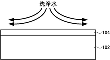
- a cross section in the manufacturing process of the semiconductor substrate 100 is shown.
- a cross section in the manufacturing process of the semiconductor substrate 100 is shown.
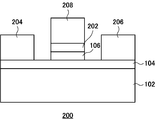
- a cross section of a field effect transistor 200 is shown.
- a cross section in the manufacturing process of the field effect transistor 200 is shown.
- 2 shows drain current-gate voltage (Id-Vg) characteristics of a field effect transistor manufactured on an InP (100) substrate.
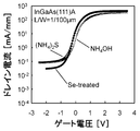
- the Id-Vg characteristics of a field effect transistor manufactured on an InP (111) A substrate are shown.
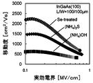
- the mobility of the field effect transistor manufactured on the InP (100) substrate is shown.
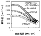
- the mobility of the field effect transistor manufactured on the InP (111) A substrate is shown.
- the temperature dependence of the mobility of the field effect transistor manufactured on the InP (100) substrate and the InP (111) A substrate is shown.
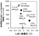
- the relationship between the mobility and threshold voltage in the high electric field region of the field effect transistor manufactured on the InP (100) substrate and the InP (111) A substrate is shown.
- the relationship between the current on-off ratio of the field effect transistor manufactured on the InP (100) substrate and the InP (111) A substrate and the interface state density estimated from the S value is shown.
- Al 2 O 3 / secondary ion mass spectrometry of InGaAs layer shows the depth profile by (SIMS).
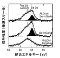
- the results of surface elemental analysis by the XPS method are shown for three cases where the surface of InGaAs on the InP substrate is treated with NH 4 OH, treated with Se cleaning liquid, and treated with Se cleaning liquid and then formed with an ALD layer. The vicinity of the Se3d peak is shown.
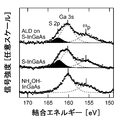
- the results of surface elemental analysis by the XPS method for the three cases where the InGaAs surface on the InP substrate was treated with NH 4 OH, treated with a sulfur cleaning solution, or treated with a sulfur cleaning solution and then formed with an ALD layer were shown. The vicinity of the S2p peak is shown.
- FIG. 1 shows a cross section of the semiconductor substrate 100.
- the semiconductor substrate 100 includes a base substrate 102, a compound semiconductor layer 104, and an insulating layer 106.
- the base substrate 102, the compound semiconductor layer 104, and the insulating layer 106 are positioned in the order of the base substrate 102, the compound semiconductor layer 104, and the insulating layer 106.
- the base substrate 102 is an InP substrate.
- InP substrate an InP (100) substrate in which the surface on which the compound semiconductor layer 104 is formed is a (100) plane, and an InP (111) A substrate in which the surface on which the compound semiconductor layer 104 is formed is a (111) A plane.
- the base substrate 102 may be a substrate whose surface is a silicon crystal. Examples of the substrate whose surface is a silicon crystal include a silicon substrate and an SOI (Silicon-on-insulator) substrate.
- Base substrate 102 may be an insulating substrate such as glass or ceramics, a conductive substrate such as metal, or a semiconductor substrate such as silicon carbide.
- the compound semiconductor layer 104 is formed on the base substrate 102 by epitaxial growth.
- Examples of the compound semiconductor layer 104 include a III-V compound semiconductor layer.
- the compound semiconductor layer 104 is made of a III-V group compound semiconductor, a high-performance MISFET with high mobility can be formed.
- As the compound semiconductor layer 104 In x Ga 1-x As (0 ⁇ x ⁇ 1) can be given.
- the insulating layer 106 is formed in contact with the compound semiconductor layer 104.
- the insulating layer 106 functions as a gate insulating layer of the MISFET, and includes, for example, an Al 2 O 3 layer formed by the ALD method.
- the insulating layer 106 is preferably Al 2 O 3 .
- the insulating layer 106 Is preferably Al 2 O 3 .
- Selenium atoms are present at the interface between the compound semiconductor layer 104 and the insulating layer 106. “Having selenium atoms at the interface” does not mean that selenium atoms are strictly present only at the interface, but selenium atoms may be present in the vicinity of the interface. Selenium atoms exist mainly on the interface side of the insulating layer 106. For example, the surface density of selenium atoms contained in the compound semiconductor layer 104 near the interface is higher than the surface density of selenium atoms contained in the insulating layer 106 near the interface.
- the selenium atoms are observed with a certain width around the interface.
- the surface density of selenium atoms at the interface between the compound semiconductor layer 104 and the insulating layer 106 is preferably 1 ⁇ 10 14 atoms / cm 2 or less.
- a base substrate 102 is prepared, and a compound semiconductor layer 104 is formed on the base substrate 102 by epitaxial growth.
- a MOCVD (Metal Organic Chemical Vapor Deposition) method can be used for the epitaxial growth of the compound semiconductor layer 104.
- TMIn trimethylindium
- TMGa trimethylgallium
- AsH 3 arsine
- Hydrogen can be used as the carrier gas.
- the reaction temperature can be appropriately selected in the range of 300 ° C. to 900 ° C., preferably in the range of 450 to 750 ° C.
- the thickness of the epitaxial growth layer can be controlled by appropriately selecting the reaction time.
- the surface of the compound semiconductor layer 104 is cleaned with a cleaning liquid containing a selenium compound.
- the selenium compound include selenium oxide.
- Selenium oxide includes H 2 SeO 3 .
- the cleaning liquid may further contain one or more substances selected from the group consisting of water, ammonia and ethanol.
- the molar concentration of the selenium compound in the cleaning liquid can be 7 ⁇ 10 ⁇ 3 mol / l or more and 7 ⁇ 10 ⁇ 1 mol / l or less.
- the insulating layer 106 is preferably made of Al 2 O 3 .
- the insulating layer 106 made of Al 2 O 3 is preferably formed by an ALD method.
- TMA trimethylaluminum
- the step of supplying only this TMA it is considered that Se atoms remaining on the surface of the compound semiconductor layer 104 by the previous cleaning process and not strongly bonded to the surface are removed. As a result, it can be expected that defects formed between the compound semiconductor layer 104 and the insulating layer 106 are reduced and the performance of the FET is improved.
- the semiconductor substrate 100 described above since the surface of the compound semiconductor layer 104 is cleaned with the cleaning liquid containing the selenium compound, the defect density at the interface with the insulating layer 106 can be reduced, and the performance of the MISFET is improved.
- FIG. 4 shows a cross section of the field effect transistor 200
- FIG. 5 shows a cross section of the field effect transistor 200 in the manufacturing process.
- the field effect transistor 200 is formed on the surface of the semiconductor substrate 100 and includes a gate electrode 202, a source electrode 204, and a drain electrode 206.
- An insulating layer 106 is located between the compound semiconductor layer 104 of the semiconductor substrate 100 and the gate electrode 202, and the insulating layer 106 functions as a gate insulating layer.
- a part of the compound semiconductor layer 104 functions as a channel.
- a gate metal 208 may be formed on the gate electrode 202.
- An example of the gate electrode 202 is TaN.
- the source electrode 204, the drain electrode 206, and the gate metal 208 are, for example, a laminated film of Ti / Au.
- the gate electrode 202 is formed by depositing a TaN film by sputtering and patterning the TaN film by lithography. Simultaneously with the patterning of the TaN film, the insulating layer 106 in the region where the source electrode 204 and the drain electrode 206 are formed is also etched away.
- the source electrode 204, the drain electrode 206, and the gate metal 208 are simultaneously formed by, for example, depositing a Ti / Au laminated film by sputtering and patterning by lift-off.
- the field effect transistor 200 can be manufactured as described above.
- the field effect transistor 200 is illustrated here as an electronic device using the semiconductor substrate 100, other electronic devices, such as a capacitor, can also be illustrated. That is, an electrode is provided on a part of the insulating layer 106, the electrode and the compound semiconductor layer 104 function as an electrode of a parallel plate capacitor, and a part of the insulating layer 106 sandwiched between the electrode and the compound semiconductor layer 104 is a capacitor. An electronic device that functions as an insulator may also be used.
- Example A field effect transistor similar to the above-described field effect transistor 200 was actually manufactured, and various analyzes and performance evaluations were performed.
- As the base substrate 102 two types of substrates, an InP (100) substrate and an InP (111) A substrate, were used.
- a p-type InGaAs layer was epitaxially grown as the compound semiconductor layer 104 on each InP substrate.
- the p-type InGaAs layer had a thickness of 0.5 ⁇ m and a p-type impurity atom concentration of 3 ⁇ 10 16 atoms / cm 3 .
- Si was ion-implanted as n-type impurity atoms in the source / drain regions.
- the ion current was adjusted so that the ion implantation amount of Si was 2 ⁇ 10 14 atoms / cm 2 .
- Impurity atoms were activated by heating at 600 ° C. for 10 seconds in a nitrogen atmosphere, and the Al 2 O 3 protective layer was removed by etching with buffered hydrofluoric acid.
- the surface of the p-type InGaAs layer was washed.
- the cleaning process was performed by immersing the InP substrate on which the p-type InGaAs layer was formed in a Se cleaning solution.
- a Se cleaning solution an NH 4 OH aqueous solution containing H 2 SeO 3 at a concentration of 4 ⁇ 10 ⁇ 2 mol / l was used.
- an Al 2 O 3 layer was formed as the insulating layer 106 by the ALD method.
- the thickness of the Al 2 O 3 layer was 12 nm and the deposition temperature was 250 ° C.
- a gate electrode made of TaN was formed by sputtering, and a source / drain electrode made of Ti / Au was formed.
- Post metal annealing was performed in a nitrogen atmosphere at 350 ° C. for 90 seconds to produce field effect transistors of Examples and Comparative Examples. The performance of the manufactured field effect transistor will be described below in comparison with the results of the comparative example.
- FIG. 6 shows the Id-Vg characteristics of the field effect transistor manufactured on the InP (100) substrate
- FIG. 7 shows the Id-Vg characteristics of the field effect transistor manufactured on the InP (111) A substrate.
- the gate length (L) and the gate width (W) of the field effect transistor are 1 ⁇ m and 100 ⁇ m, respectively. From FIG. 6 and FIG. 7, a significant reduction in off-current was observed when the Se cleaning liquid was used, compared to the case of the sulfur cleaning liquid. In particular, the effect of reducing the off-current is large in an InP (100) substrate.
- FIG. 8 shows the mobility of a field effect transistor manufactured on an InP (100) substrate
- FIG. 9 shows the mobility of a field effect transistor manufactured on an InP (111) A substrate.
- the gate length and the gate width of the field effect transistor are 100 ⁇ m and 100 ⁇ m, respectively. From FIG. 8 and FIG. 9, the effect of improving the mobility of the sulfur cleaning liquid as compared with the case of the NH 4 OH cleaning liquid can be confirmed. Further, in the case of the Se cleaning liquid, the effect of improving the mobility exceeding the effect of the sulfur cleaning liquid could be observed.
- the effective mobility at an electric field strength of 0.6 MV / cm in the case of the Se cleaning liquid was 1034 cm 2 / Vs in the case of the InP (111) A substrate and 837 cm 2 / Vs in the case of the InP (100) substrate.
- the effective mobility value of the former is 2.7 times that of the case where silicon is used as the active layer.
- FIG. 10 shows the temperature dependence of the mobility of field effect transistors fabricated on InP (100) and InP (111) A substrates.
- FIG. 11 shows the relationship between the mobility and the threshold voltage in a high electric field region of field effect transistors manufactured on an InP (100) substrate and an InP (111) A substrate.
- the mobility of the field effect transistor hardly changes in both the InP (100) substrate and the InP (111) A substrate, and the temperature dependence It was observed that the sex was not great. This result is consistent with the knowledge already obtained by the present inventors that scattering of carriers moving through the channel is mainly caused by roughness and dipole fluctuations at the interface with the insulating layer.
- the inventors have also found that when a MISFET is configured using an interface with small dipole fluctuation, the threshold voltage shifts to the negative voltage side. From FIG. 11, it can be seen that the mobility improves as the threshold voltage shifts to the negative voltage side, and that the dipolar fluctuation, which is one of the forms of defects at the MIS interface, is suppressed by the Se cleaning liquid treatment. It is suggested.
- FIG. 12 shows the relationship between the current on / off ratio of field effect transistors manufactured on InP (100) and InP (111) A substrates and the interface state density estimated from the S value.
- the S value indicates the rate of change of the drain current with respect to the gate voltage in a region below the threshold voltage, and the interface state density can be calculated from this value.
- the Se cleaning liquid treatment is the most common. Good results were shown.
- FIG. 13 shows the depth profile by secondary ion mass spectrometry (SIMS) of the Al 2 O 3 / InGaAs layer.
- SIMS secondary ion mass spectrometry
- FIG. 14 shows the surface elemental analysis by XPS method in three cases where the InGaAs surface on the InP substrate is treated with NH 4 OH, treated with Se cleaning solution, and formed with ALD layer after treatment with Se cleaning solution. This shows the vicinity of the Se3d peak.
- FIG. 15 shows the surface elemental analysis by XPS method in three cases where the InGaAs surface on the InP substrate is treated with NH 4 OH, treated with a sulfur cleaning solution, and treated with a sulfur cleaning solution and then formed with an ALD layer. This shows the vicinity of the S2p peak.
- the concentration of Se atoms at the interface estimated from the XPS intensity shown in FIG. 14 corresponds to about 0.2 monolayer (surface density of about 1 ⁇ 10 14 atoms / cm 2 ).
- the concentration of sulfur atoms at the interface estimated from the XPS intensity in FIG. 15 corresponds to about 0.6 monolayer. From this point, it can be inferred that the amount of Se atoms contained in the interface in the case of the Se cleaning liquid is smaller than the amount of sulfur atoms contained in the interface in the case of the sulfur cleaning liquid. This is the case when using the Se cleaning liquid compared to the sulfur cleaning liquid. It is considered that this is one of the reasons why the performance improvement of the field effect transistor is achieved.
- the mobility of the field effect transistor can be increased and the current on / off ratio can be increased.
- semiconductor substrate 100 semiconductor substrate, 102 base substrate, 104 compound semiconductor layer, 106 insulating layer, 200 field effect transistor, 202 gate electrode, 204 source electrode, 206 drain electrode, 208 gate metal
Landscapes
- Insulated Gate Type Field-Effect Transistor (AREA)
- Thin Film Transistor (AREA)
- Recrystallisation Techniques (AREA)
Abstract
エピタキシャル成長により化合物半導体層をベース基板上に形成するステップと、化合物半導体層の表面をセレン化合物を含む洗浄液で洗浄するステップと、化合物半導体層の表面上に絶縁層を形成するステップと、を有する半導体基板の製造方法を提供する。セレン化合物として、セレン酸化物が挙げられる。セレン酸化物として、H2SeO3が挙げられる。洗浄液が、水、アンモニアおよびエタノールからなる群から選択された1以上の物質をさらに含んでもよい。化合物半導体層の表面がInxGa1-xAs(0≦x≦1)からなる場合、絶縁層がAl2O3からなるものであることが好ましく、Al2O3は、ALD法により形成されることが好ましい。
Description
本発明は、半導体基板の製造方法および半導体基板に関する。
非特許文献1~3には、(NH4)2S、HBrあるいは窒化リンを用いて、MISFET(Metal-Insulator-Semiconductor Field-Effect Transistor)に用いるIII-V族化合物半導体の表面を不動態化するパッシベーション技術が記載されている。
非特許文献1 Y.Xuan et al.,IEEE Electron Device Lett.,28,935(2007)
非特許文献2 Y.Q.Wu et al.,IEDM Tech.Dig.,323(2009)
非特許文献3 H.J.Oh et al.,IEDM Tech.Dig.,339(2009)
非特許文献1 Y.Xuan et al.,IEEE Electron Device Lett.,28,935(2007)
非特許文献2 Y.Q.Wu et al.,IEDM Tech.Dig.,323(2009)
非特許文献3 H.J.Oh et al.,IEDM Tech.Dig.,339(2009)
上記したパッシベーション技術により、III-V族化合物半導体と絶縁層との界面における欠陥密度が低減され、III-V族化合物半導体層をチャネル層に用いるIII-V族MISFETの性能が向上すると期待される。
しかし、より効果的にIII-V族化合物半導体の表面を不動態化するパッシベーション技術が望まれる。より効果的なパッシベーション技術を適用して、III-V族MISFETの性能を向上することが期待される。
本発明の目的は、高性能なIII-V族MISFETの実現を可能にする、より効果的なIII-V族化合物半導体表面のパッシベーション技術を提供することにある。
上記課題を解決するために、本発明の第1の態様においては、エピタキシャル成長により化合物半導体層をベース基板上に形成するステップと、化合物半導体層の表面をセレン化合物を含む洗浄液で洗浄するステップと、化合物半導体層の表面上に絶縁層を形成するステップと、を有する半導体基板の製造方法が提供される。
セレン化合物として、セレン酸化物が挙げられる。セレン酸化物として、H2SeO3が挙げられる。洗浄液が、水、アンモニアおよびエタノールからなる群から選択された1以上の物質をさらに含んでもよい。洗浄液中のセレン化合物のモル濃度が、7×10―3mol/l以上7×10―1mol/l以下であることが好ましい。化合物半導体層の表面がInxGa1-xAs(0≦x≦1)からなる場合、絶縁層がAl2O3からなるものであることが好ましい。絶縁層を形成するステップとして、ALD(atomic layer deposition)法(原子層堆積法)により絶縁層を形成するステップが挙げられる。
本発明の第2の態様においては、化合物半導体層と、化合物半導体層に接する絶縁層と、を有し、化合物半導体層と絶縁層との界面にセレン原子を有する半導体基板が提供される。化合物半導体層と絶縁層との界面におけるセレン原子の面密度は、1×10¹⁴atoms/cm2以下であることが好ましい。化合物半導体層の表面がInxGa1-xAs(0≦x≦1)からなる場合、絶縁層がAl2O3からなるものであることが好ましい。
図1は、半導体基板100の断面を示す。半導体基板100は、ベース基板102と、化合物半導体層104と、絶縁層106とを有する。ベース基板102、化合物半導体層104および絶縁層106は、ベース基板102、化合物半導体層104、絶縁層106の順に位置する。
ベース基板102として、InP基板が挙げられる。InP基板として、化合物半導体層104が形成される面が(100)面であるInP(100)基板、化合物半導体層104が形成される面が(111)A面であるInP(111)A基板が挙げられる。ベース基板102は、表面がシリコン結晶である基板であってもよい。表面がシリコン結晶である基板として、シリコン基板、SOI(Silicon on Insulator)基板が挙げられる。ベース基板102は、ガラス、セラミックス等の絶縁体基板、金属等の導電体基板、炭化シリコン等の半導体基板であってもよい。
化合物半導体層104は、エピタキシャル成長によりベース基板102上に形成される。化合物半導体層104として、III-V族化合物半導体層が挙げられる。化合物半導体層104をIII-V族化合物半導体からなるものとすることで、移動度の大きい高性能なMISFETを形成できる。化合物半導体層104として、InxGa1-xAs(0≦x≦1)が挙げられる。
絶縁層106は、化合物半導体層104に接して形成される。絶縁層106は、MISFETのゲート絶縁層として機能するものであり、たとえばALD法により形成されたAl2O3層が挙げられる。なお、化合物半導体層104の表面がInxGa1-xAs(0≦x≦1)からなる場合、絶縁層106はAl2O3であることが好ましい。化合物半導体層104が複数の化合物半導体層からなる積層構造の場合においても、その最も上の化合物半導体層の表面がInxGa1-xAs(0≦x≦1)からなるとき、絶縁層106はAl2O3であることが好ましい。
化合物半導体層104と絶縁層106との界面にセレン原子を有する。「界面にセレン原子を有する」とは、厳密に界面にのみセレン原子が存在することを意味するのではなく、界面近傍にセレン原子が存在すればよい。また、セレン原子は、主に絶縁層106の界面側に存在する。例えば界面近傍の化合物半導体層104に含まれるセレン原子の面密度は、界面近傍の絶縁層106に含まれるセレン原子の面密度より高い。セレン原子の存在位置をたとえばSIMS(二次イオン質量分析)による深さプロファイルで分析すれば、界面近傍を中心にある程度の幅を持って観測される。化合物半導体層104と絶縁層106との界面におけるセレン原子の面密度は、1×10¹⁴atoms/cm2以下であることが好ましい。
図2および図3は、半導体基板100の製造過程における断面を示す。図2に示すように、ベース基板102を用意し、エピタキシャル成長により化合物半導体層104をベース基板102上に形成する。化合物半導体層104のエピタキシャル成長には、MOCVD(Metal Organic Chemical Vapor Deposition)法を利用することができる。MOCVD法において、InソースにはTMIn(トリメチルインジウム)を、GaソースにはTMGa(トリメチルガリウム)を、AsソースにはAsH3(アルシン)を用いることができる。キャリアガスには水素を用いることができる。反応温度は、300℃から900℃の範囲で、好ましくは450~750℃の範囲で適宜選択できる。反応時間を適宜選択することでエピタキシャル成長層の厚さを制御することができる。
図3に示すように、化合物半導体層104の表面をセレン化合物を含む洗浄液で洗浄する。セレン化合物として、セレン酸化物が挙げられる。セレン酸化物として、H2SeO3が挙げられる。また、洗浄液には、水、アンモニアおよびエタノールからなる群から選択された1以上の物質をさらに含んでもよい。洗浄液中のセレン化合物のモル濃度は、7×10―3mol/l以上7×10―1mol/l以下とすることができる。そして、化合物半導体層104の上に絶縁層106を形成し、図1に示す半導体基板100が製造できる。
なお、化合物半導体層104の表面がInxGa1-xAs(0≦x≦1)からなる場合、絶縁層106は、Al2O3からなることが望ましい。この場合、Al2O3からなる絶縁層106は、ALD法により形成することが好ましい。ALD法によるAl2O3層の形成では、層形成の最初のステップにおいて、Al原料であるTMA(トリメチルアルミニウム)のみを供給する。このTMAのみを供給するステップにおいて、先の洗浄処理で化合物半導体層104の表面に残留し、同表面に強く結合していないSe原子が除去されると考えられる。この結果、化合物半導体層104と絶縁層106との間に形成される欠陥が減少し、FETの性能が向上することが期待できる。
以上説明した半導体基板100によれば、化合物半導体層104の表面をセレン化合物を含む洗浄液で洗浄するため、絶縁層106との界面における欠陥密度が低減でき、MISFETの性能が向上する。
図4は、電界効果トランジスタ200の断面を示し、図5は、電界効果トランジスタ200の製造過程における断面を示す。電界効果トランジスタ200は、半導体基板100の表面に形成され、ゲート電極202、ソース電極204、ドレイン電極206を有する。半導体基板100の化合物半導体層104とゲート電極202との間には絶縁層106が位置し、絶縁層106はゲート絶縁層として機能する。化合物半導体層104の一部はチャネルとして機能する。ゲート電極202の上にはゲート金属208が形成されても良い。ゲート電極202として、TaNが挙げられる。ソース電極204、ドレイン電極206およびゲート金属208は、たとえばTi/Auの積層膜である。
図5に示すように、半導体基板100を製造した後、ゲート電極202を、スパッタ法によるTaN膜の堆積およびリソグラフィによるTaN膜のパターニングにより形成する。TaN膜のパターニングと同時に、ソース電極204およびドレイン電極206が形成される領域の絶縁層106もエッチングして除去する。
次に、たとえばスパッタ法によるTi/Au積層膜の膜堆積およびリフトオフ法によるパターニングにより、ソース電極204、ドレイン電極206およびゲート金属208を同時に形成する。以上のようにして、電界効果トランジスタ200が製造できる。
なお、ここでは、半導体基板100を用いる電子デバイスとして電界効果トランジスタ200を例示しているが、キャパシタ等他の電子デバイスも例示できる。すなわち、絶縁層106の一部上に電極を有し、当該電極と化合物半導体層104が平行平板キャパシタの電極として機能し、電極と化合物半導体層104で挟まれた絶縁層106の一部がキャパシタ絶縁体として機能するような電子デバイスであっても良い。
(実施例)
上記した電界効果トランジスタ200と同様な電界効果トランジスタを実際に製造し、各種の分析と性能評価を実施した。ベース基板102として、InP(100)基板とInP(111)A基板の二種類の基板を用いた。各々のInP基板上に、化合物半導体層104としてp形InGaAs層をエピタキシャル成長した。p型InGaAs層は、厚さを0.5μmとし、p型不純物原子の濃度を3×10¹⁶atoms/cm3とした。ALD法により厚さ6nmのAl2O3保護層を形成した後、ソース・ドレイン領域にn型不純物原子としてSiをイオン注入した。Siのイオン注入量が2×1014atoms/cm2となるようにイオン電流を調整した。窒素雰囲気での600℃、10秒の加熱により不純物原子を活性化し、Al2O3保護層を緩衝フッ酸によるエッチングにより除去した。
上記した電界効果トランジスタ200と同様な電界効果トランジスタを実際に製造し、各種の分析と性能評価を実施した。ベース基板102として、InP(100)基板とInP(111)A基板の二種類の基板を用いた。各々のInP基板上に、化合物半導体層104としてp形InGaAs層をエピタキシャル成長した。p型InGaAs層は、厚さを0.5μmとし、p型不純物原子の濃度を3×10¹⁶atoms/cm3とした。ALD法により厚さ6nmのAl2O3保護層を形成した後、ソース・ドレイン領域にn型不純物原子としてSiをイオン注入した。Siのイオン注入量が2×1014atoms/cm2となるようにイオン電流を調整した。窒素雰囲気での600℃、10秒の加熱により不純物原子を活性化し、Al2O3保護層を緩衝フッ酸によるエッチングにより除去した。
次にp型InGaAs層の表面を洗浄処理した。洗浄処理は、p型InGaAs層を形成したInP基板をSe洗浄液に浸漬することで実施した。Se洗浄液として、H2SeO3を4×10⁻²mol/lの濃度で含有するNH4OH水溶液を用いた。なお比較例として、H2SeO3を(NH4)2Sに代えたイオウ洗浄液を用いた場合のサンプル(比較例1)と、NH4OH水溶液のみを洗浄液として用いた場合のサンプル(比較例2)も作成した。
洗浄処理の後、絶縁層106としてAl2O3層をALD法により形成した。Al2O3層の厚さは12nmとし、堆積温度は250℃とした。スパッタ法によりTaNからなるゲート電極を形成し、Ti/Auからなるソース・ドレイン電極を形成した。窒素雰囲気、350℃、90秒のポストメタルアニールを行い、実施例および比較例の電界効果トランジスタを製造した。以下製造した電界効果トランジスタの性能を比較例の結果と比較しながら説明する。
図6は、InP(100)基板上に製造した電界効果トランジスタのId-Vg特性を示し、図7は、InP(111)A基板上に製造した電界効果トランジスタのId-Vg特性を示す。なお、図6、図7において、電界効果トランジスタのゲート長(L)およびゲート幅(W)はそれぞれ1μmおよび100μmである。図6および図7から、イオウ洗浄液の場合に比較して、Se洗浄液を用いた場合には顕著なオフ電流の低減が観察された。特にInP(100)基板においてオフ電流低減の効果が大きい。
図8は、InP(100)基板上に製造した電界効果トランジスタの移動度を示し、図9は、InP(111)A基板上に製造した電界効果トランジスタの移動度を示す。なお、図8、図9において、電界効果トランジスタのゲート長およびゲート幅はそれぞれ100μmおよび100μmである。図8および図9から、NH4OH洗浄液の場合と比較したイオウ洗浄液の移動度向上効果が確認できる。さらに、Se洗浄液の場合、イオウ洗浄液の効果を上回る移動度向上の効果が観察できた。Se洗浄液の場合の0.6MV/cmの電界強度における実効移動度は、InP(111)A基板の場合で1034cm2/Vs、InP(100)基板の場合で837cm2/Vsであった。前者の実効移動度の値は、シリコンを活性層とする場合と比較して2.7倍の値である。
図10は、InP(100)基板およびInP(111)A基板上に製造した電界効果トランジスタの移動度の温度依存性を示す。図11は、InP(100)基板およびInP(111)A基板上に製造した電界効果トランジスタの高電界域における移動度としきい値電圧との関係を示す。図10に示すように、温度を80kから300kまで変化させても、InP(100)基板およびInP(111)A基板の双方において、電界効果トランジスタの移動度はほとんど変化しておらず、温度依存性は大きくないことが観察された。この結果は、チャネルを移動するキャリアの散乱は、主に絶縁層との界面におけるラフネスと双極子ゆらぎに起因するという、本発明者らが既に得ている知見と整合する。また、本発明者らは、双極子ゆらぎが小さい界面を用いてMISFETを構成した場合、しきい値電圧が負電圧側にシフトするという知見も得ている。図11から、しきい値電圧が負電圧側にシフトするほど移動度が改善することが分かり、Se洗浄液処理によってMIS界面における欠陥の形態の一つである双極子ゆらぎが抑制されていることが示唆される。
図12は、InP(100)基板およびInP(111)A基板上に製造した電界効果トランジスタの電流オンオフ比とS値から推計した界面準位密度との関係を示す。ここで、S値とはしきい値電圧以下の領域でのゲート電圧に対するドレイン電流の変化率を指し、この値から界面準位密度を計算することができる。図12に示すように、界面準位密度が大きくなると電流オンオフ比が低下する傾向が確認され、また、InP(100)基板およびInP(111)A基板のそれぞれにおいて、Se洗浄液処理の場合が最も良好な結果を示した。
図13は、Al2O3/InGaAs層の二次イオン質量分析(SIMS)による深さプロファイルを示す。InP(100)基板上にInGaAs層を形成し、Se洗浄液による洗浄後にAl2O3層を形成して、Al2O3/InGaAs層を形成した。図13に示す深さプロファイルから、Al2O3層とInGaAs層との界面にSe原子が残留していることが分かった。
図14は、InP基板上のInGaAs表面をNH4OH処理した場合、Se洗浄液処理した場合、Se洗浄液処理した後にALD層を形成した場合の三通りの場合について、XPS法による表面元素分析を行った結果であって、Se3dピークの近傍を示したものである。図15は、InP基板上のInGaAs表面をNH4OH処理した場合、イオウ洗浄液処理した場合、イオウ洗浄液処理した後ALD層を形成した場合の三通りの場合について、XPS法による表面元素分析を行った結果であって、S2pピークの近傍を示したものである。
図14に示すXPS強度から推計された、界面におけるSe原子の濃度は、約0.2モノレイヤー(面密度約1×10¹⁴atoms/cm2)に相当した。一方、図15のXPS強度から推計された界面におけるイオウ原子の濃度は、約0.6モノレイヤーに相当した。この点からSe洗浄液の場合に界面に含まれるSe原子の量は、イオウ洗浄液の場合に界面に含まれるイオウ原子の量より少ないと推察でき、これがイオウ洗浄液に比較してSe洗浄液を用いた場合に電界効果トランジスタの性能向上が達成される一因と考えられる。
また、Se洗浄液中のH2SeO3の濃度を1×10⁻¹mol/l、および3×10-1mol/lとした場合について同様にサンプルを作成し、製造した電界効果トランジスタの性能を確認した。その結果、いずれの場合においてもH2SeO3濃度が4×10-2mol/lの場合と同様の性能が得られた。
本発明の半導体基板の製造方法によれば、MIS界面の洗浄をSe洗浄液を用いて行うので、電界効果トランジスタの移動度を高くし、電流オンオフ比を高くすることができる。
100 半導体基板、102 ベース基板、104 化合物半導体層、106 絶縁層、200 電界効果トランジスタ、202 ゲート電極、204 ソース電極、206 ドレイン電極、208 ゲート金属
Claims (10)
- エピタキシャル成長により化合物半導体層をベース基板上に形成するステップと、
前記化合物半導体層の表面をセレン化合物を含む洗浄液で洗浄するステップと、
前記化合物半導体層の表面上に絶縁層を形成するステップと、を有する
半導体基板の製造方法。 - 前記セレン化合物が、セレン酸化物である
請求項1に記載の半導体基板の製造方法。 - 前記セレン酸化物が、H2SeO3である
請求項2に記載の半導体基板の製造方法。 - 前記洗浄液が、水、アンモニアおよびエタノールからなる群から選択された1以上の物質をさらに含む
請求項1に記載の半導体基板の製造方法。 - 前記洗浄液中のセレン化合物のモル濃度が、7×10―3mol/l以上7×10―1mol/l以下である
請求項1に記載の半導体基板の製造方法。 - 前記化合物半導体層の表面がInxGa1-xAs(0≦x≦1)からなり、
前記絶縁層がAl2O3からなる
請求項1に記載の半導体基板の製造方法。 - 前記絶縁層を形成するステップが、ALD法により前記絶縁層を形成するステップである
請求項1に記載の半導体基板の製造方法。 - 化合物半導体層と、
前記化合物半導体層に接する絶縁層と、を有し、
前記化合物半導体層と前記絶縁層との界面にセレン原子を有する
半導体基板。 - 前記化合物半導体層と前記絶縁層との界面における前記セレン原子の面密度が、1×10¹⁴atoms/cm2以下である
請求項8に記載の半導体基板。 - 前記化合物半導体層の表面がInxGa1-xAs(0≦x≦1)からなり、
前記絶縁層がAl2O3からなる
請求項8に記載の半導体基板。
Priority Applications (3)
| Application Number | Priority Date | Filing Date | Title |
|---|---|---|---|
| KR1020137030880A KR20140048122A (ko) | 2011-06-10 | 2012-06-08 | 반도체 기판의 제조 방법 및 반도체 기판 |
| CN201280024373.1A CN103548126B (zh) | 2011-06-10 | 2012-06-08 | 半导体基板的制造方法及半导体基板 |
| US14/099,425 US9184240B2 (en) | 2011-06-10 | 2013-12-06 | Method of producing semiconductor wafer, and semiconductor wafer |
Applications Claiming Priority (2)
| Application Number | Priority Date | Filing Date | Title |
|---|---|---|---|
| JP2011-130726 | 2011-06-10 | ||
| JP2011130726A JP2013004545A (ja) | 2011-06-10 | 2011-06-10 | 半導体基板の製造方法および半導体基板 |
Related Child Applications (1)
| Application Number | Title | Priority Date | Filing Date |
|---|---|---|---|
| US14/099,425 Continuation-In-Part US9184240B2 (en) | 2011-06-10 | 2013-12-06 | Method of producing semiconductor wafer, and semiconductor wafer |
Publications (1)
| Publication Number | Publication Date |
|---|---|
| WO2012169208A1 true WO2012169208A1 (ja) | 2012-12-13 |
Family
ID=47295791
Family Applications (1)
| Application Number | Title | Priority Date | Filing Date |
|---|---|---|---|
| PCT/JP2012/003768 Ceased WO2012169208A1 (ja) | 2011-06-10 | 2012-06-08 | 半導体基板の製造方法および半導体基板 |
Country Status (6)
| Country | Link |
|---|---|
| US (1) | US9184240B2 (ja) |
| JP (1) | JP2013004545A (ja) |
| KR (1) | KR20140048122A (ja) |
| CN (1) | CN103548126B (ja) |
| TW (1) | TWI549194B (ja) |
| WO (1) | WO2012169208A1 (ja) |
Families Citing this family (4)
| Publication number | Priority date | Publication date | Assignee | Title |
|---|---|---|---|---|
| JP2014187238A (ja) * | 2013-03-25 | 2014-10-02 | Toyoda Gosei Co Ltd | Mis型半導体装置の製造方法 |
| WO2014192311A1 (ja) * | 2013-05-31 | 2014-12-04 | 住友化学株式会社 | 半導体基板、半導体基板の製造方法および電子デバイス |
| US9245742B2 (en) | 2013-12-18 | 2016-01-26 | Asm Ip Holding B.V. | Sulfur-containing thin films |
| CN107706267A (zh) * | 2017-07-24 | 2018-02-16 | 晶科能源有限公司 | 一种硅片表面钝化方法 |
Citations (4)
| Publication number | Priority date | Publication date | Assignee | Title |
|---|---|---|---|---|
| JPH06140375A (ja) * | 1992-10-22 | 1994-05-20 | Nec Corp | 化合物半導体の表面処理方法 |
| JPH08250459A (ja) * | 1995-03-08 | 1996-09-27 | Nippon Telegr & Teleph Corp <Ntt> | 半導体のエッチング方法およびそれを用いた薄膜形成方法 |
| JP2004342733A (ja) * | 2003-05-14 | 2004-12-02 | Hitachi Ltd | 半導体装置の製造方法及びその製造方法による半導体装置 |
| JP2009260325A (ja) * | 2008-03-26 | 2009-11-05 | Univ Of Tokyo | 半導体基板、半導体基板の製造方法および半導体装置 |
Family Cites Families (4)
| Publication number | Priority date | Publication date | Assignee | Title |
|---|---|---|---|---|
| US3915765A (en) * | 1973-06-25 | 1975-10-28 | Bell Telephone Labor Inc | MBE technique for fabricating semiconductor devices having low series resistance |
| US5616947A (en) * | 1994-02-01 | 1997-04-01 | Matsushita Electric Industrial Co., Ltd. | Semiconductor device having an MIS structure |
| US8236599B2 (en) * | 2009-04-09 | 2012-08-07 | State of Oregon acting by and through the State Board of Higher Education | Solution-based process for making inorganic materials |
| EP2306497B1 (en) * | 2009-10-02 | 2012-06-06 | Imec | Method for manufacturing a low defect interface between a dielectric and a III/V compound |
-
2011
- 2011-06-10 JP JP2011130726A patent/JP2013004545A/ja not_active Ceased
-
2012
- 2012-06-08 TW TW101120840A patent/TWI549194B/zh not_active IP Right Cessation
- 2012-06-08 KR KR1020137030880A patent/KR20140048122A/ko not_active Withdrawn
- 2012-06-08 WO PCT/JP2012/003768 patent/WO2012169208A1/ja not_active Ceased
- 2012-06-08 CN CN201280024373.1A patent/CN103548126B/zh not_active Expired - Fee Related
-
2013
- 2013-12-06 US US14/099,425 patent/US9184240B2/en not_active Expired - Fee Related
Patent Citations (4)
| Publication number | Priority date | Publication date | Assignee | Title |
|---|---|---|---|---|
| JPH06140375A (ja) * | 1992-10-22 | 1994-05-20 | Nec Corp | 化合物半導体の表面処理方法 |
| JPH08250459A (ja) * | 1995-03-08 | 1996-09-27 | Nippon Telegr & Teleph Corp <Ntt> | 半導体のエッチング方法およびそれを用いた薄膜形成方法 |
| JP2004342733A (ja) * | 2003-05-14 | 2004-12-02 | Hitachi Ltd | 半導体装置の製造方法及びその製造方法による半導体装置 |
| JP2009260325A (ja) * | 2008-03-26 | 2009-11-05 | Univ Of Tokyo | 半導体基板、半導体基板の製造方法および半導体装置 |
Also Published As
| Publication number | Publication date |
|---|---|
| US20140091433A1 (en) | 2014-04-03 |
| CN103548126B (zh) | 2016-06-22 |
| JP2013004545A (ja) | 2013-01-07 |
| KR20140048122A (ko) | 2014-04-23 |
| CN103548126A (zh) | 2014-01-29 |
| US9184240B2 (en) | 2015-11-10 |
| TW201306135A (zh) | 2013-02-01 |
| TWI549194B (zh) | 2016-09-11 |
Similar Documents
| Publication | Publication Date | Title |
|---|---|---|
| JP7434679B2 (ja) | ノーマリーオフiii-窒化物トランジスタ | |
| JP5545713B2 (ja) | 半導体基板、半導体基板の製造方法および電子デバイス | |
| US9130026B2 (en) | Crystalline layer for passivation of III-N surface | |
| Huang et al. | Low-Leakage-Current AIN/GaN MOSHFETs Using A12O3 for Increased 2DEG | |
| Chin et al. | III–V Multiple-Gate Field-Effect Transistors With High-Mobility $\hbox {In} _ {0.7}\hbox {Ga} _ {0.3}\hbox {As} $ Channel and Epi-Controlled Retrograde-Doped Fin | |
| Huang et al. | Vertically stacked strained 3-GeSn-nanosheet pGAAFETs on Si using GeSn/Ge CVD epitaxial growth and the optimum selective channel release process | |
| CN102709321A (zh) | 增强型开关器件及其制造方法 | |
| CN105122456A (zh) | 第iii族氮化物常关晶体管的层结构 | |
| US20140091392A1 (en) | Semiconductor device, semiconductor wafer, method for producing semiconductor wafer, and method for producing semiconductor device | |
| JP2009010107A (ja) | 半導体装置及びその製造方法 | |
| JP6560117B2 (ja) | 半導体装置の製造方法 | |
| US9755040B2 (en) | Semiconductor wafer, method of producing semiconductor wafer and electronic device | |
| KR20140027938A (ko) | 반도체 기판, 전계 효과 트랜지스터, 반도체 기판의 제조 방법, 및 전계 효과 트랜지스터의 제조 방법 | |
| US20150028387A1 (en) | III-V FET Device with Overlapped Extension Regions Using Gate Last | |
| US9184240B2 (en) | Method of producing semiconductor wafer, and semiconductor wafer | |
| US9553181B2 (en) | Crystalline-amorphous transition material for semiconductor devices and method for formation | |
| JP2009076673A (ja) | Iii族窒化物半導体を用いた電界効果トランジスタ | |
| CN103855022A (zh) | 鳍式场效应晶体管的形成方法 | |
| US20140264638A1 (en) | Gate stack of boron semiconductor alloy, polysilicon and high-k gate dielectric for low voltage applications | |
| CN102544103A (zh) | 一种InP反型n沟道场效应管及其制备方法 | |
| JP2011166005A (ja) | 窒化物半導体を用いた半導体装置およびその製造方法 | |
| Huang et al. | Investigation of AlGaN/GaN/AlGaN metal-oxide-semiconductor high electron mobility transistors | |
| JP2013084951A (ja) | 半導体装置および半導体装置の製造方法 |
Legal Events
| Date | Code | Title | Description |
|---|---|---|---|
| 121 | Ep: the epo has been informed by wipo that ep was designated in this application |
Ref document number: 12796607 Country of ref document: EP Kind code of ref document: A1 |
|
| ENP | Entry into the national phase |
Ref document number: 20137030880 Country of ref document: KR Kind code of ref document: A |
|
| NENP | Non-entry into the national phase |
Ref country code: DE |
|
| 122 | Ep: pct application non-entry in european phase |
Ref document number: 12796607 Country of ref document: EP Kind code of ref document: A1 |