WO2012165328A1 - Load driving device and electronic device using same - Google Patents
Load driving device and electronic device using same Download PDFInfo
- Publication number
- WO2012165328A1 WO2012165328A1 PCT/JP2012/063471 JP2012063471W WO2012165328A1 WO 2012165328 A1 WO2012165328 A1 WO 2012165328A1 JP 2012063471 W JP2012063471 W JP 2012063471W WO 2012165328 A1 WO2012165328 A1 WO 2012165328A1
- Authority
- WO
- WIPO (PCT)
- Prior art keywords
- power supply
- supply voltage
- detection signal
- transistor
- driving device
- Prior art date
Links
Images


Classifications
-
- H—ELECTRICITY
- H02—GENERATION; CONVERSION OR DISTRIBUTION OF ELECTRIC POWER
- H02H—EMERGENCY PROTECTIVE CIRCUIT ARRANGEMENTS
- H02H7/00—Emergency protective circuit arrangements specially adapted for specific types of electric machines or apparatus or for sectionalised protection of cable or line systems, and effecting automatic switching in the event of an undesired change from normal working conditions
- H02H7/10—Emergency protective circuit arrangements specially adapted for specific types of electric machines or apparatus or for sectionalised protection of cable or line systems, and effecting automatic switching in the event of an undesired change from normal working conditions for converters; for rectifiers
- H02H7/12—Emergency protective circuit arrangements specially adapted for specific types of electric machines or apparatus or for sectionalised protection of cable or line systems, and effecting automatic switching in the event of an undesired change from normal working conditions for converters; for rectifiers for static converters or rectifiers
- H02H7/122—Emergency protective circuit arrangements specially adapted for specific types of electric machines or apparatus or for sectionalised protection of cable or line systems, and effecting automatic switching in the event of an undesired change from normal working conditions for converters; for rectifiers for static converters or rectifiers for inverters, i.e. dc/ac converters
-
- H—ELECTRICITY
- H02—GENERATION; CONVERSION OR DISTRIBUTION OF ELECTRIC POWER
- H02M—APPARATUS FOR CONVERSION BETWEEN AC AND AC, BETWEEN AC AND DC, OR BETWEEN DC AND DC, AND FOR USE WITH MAINS OR SIMILAR POWER SUPPLY SYSTEMS; CONVERSION OF DC OR AC INPUT POWER INTO SURGE OUTPUT POWER; CONTROL OR REGULATION THEREOF
- H02M1/00—Details of apparatus for conversion
- H02M1/32—Means for protecting converters other than automatic disconnection
-
- H—ELECTRICITY
- H02—GENERATION; CONVERSION OR DISTRIBUTION OF ELECTRIC POWER
- H02M—APPARATUS FOR CONVERSION BETWEEN AC AND AC, BETWEEN AC AND DC, OR BETWEEN DC AND DC, AND FOR USE WITH MAINS OR SIMILAR POWER SUPPLY SYSTEMS; CONVERSION OF DC OR AC INPUT POWER INTO SURGE OUTPUT POWER; CONTROL OR REGULATION THEREOF
- H02M1/00—Details of apparatus for conversion
- H02M1/08—Circuits specially adapted for the generation of control voltages for semiconductor devices incorporated in static converters
-
- H—ELECTRICITY
- H02—GENERATION; CONVERSION OR DISTRIBUTION OF ELECTRIC POWER
- H02M—APPARATUS FOR CONVERSION BETWEEN AC AND AC, BETWEEN AC AND DC, OR BETWEEN DC AND DC, AND FOR USE WITH MAINS OR SIMILAR POWER SUPPLY SYSTEMS; CONVERSION OF DC OR AC INPUT POWER INTO SURGE OUTPUT POWER; CONTROL OR REGULATION THEREOF
- H02M1/00—Details of apparatus for conversion
- H02M1/0003—Details of control, feedback or regulation circuits
- H02M1/0006—Arrangements for supplying an adequate voltage to the control circuit of converters
-
- H—ELECTRICITY
- H02—GENERATION; CONVERSION OR DISTRIBUTION OF ELECTRIC POWER
- H02M—APPARATUS FOR CONVERSION BETWEEN AC AND AC, BETWEEN AC AND DC, OR BETWEEN DC AND DC, AND FOR USE WITH MAINS OR SIMILAR POWER SUPPLY SYSTEMS; CONVERSION OF DC OR AC INPUT POWER INTO SURGE OUTPUT POWER; CONTROL OR REGULATION THEREOF
- H02M1/00—Details of apparatus for conversion
- H02M1/36—Means for starting or stopping converters
-
- H—ELECTRICITY
- H02—GENERATION; CONVERSION OR DISTRIBUTION OF ELECTRIC POWER
- H02M—APPARATUS FOR CONVERSION BETWEEN AC AND AC, BETWEEN AC AND DC, OR BETWEEN DC AND DC, AND FOR USE WITH MAINS OR SIMILAR POWER SUPPLY SYSTEMS; CONVERSION OF DC OR AC INPUT POWER INTO SURGE OUTPUT POWER; CONTROL OR REGULATION THEREOF
- H02M3/00—Conversion of dc power input into dc power output
- H02M3/02—Conversion of dc power input into dc power output without intermediate conversion into ac
- H02M3/04—Conversion of dc power input into dc power output without intermediate conversion into ac by static converters
- H02M3/10—Conversion of dc power input into dc power output without intermediate conversion into ac by static converters using discharge tubes with control electrode or semiconductor devices with control electrode
- H02M3/145—Conversion of dc power input into dc power output without intermediate conversion into ac by static converters using discharge tubes with control electrode or semiconductor devices with control electrode using devices of a triode or transistor type requiring continuous application of a control signal
- H02M3/155—Conversion of dc power input into dc power output without intermediate conversion into ac by static converters using discharge tubes with control electrode or semiconductor devices with control electrode using devices of a triode or transistor type requiring continuous application of a control signal using semiconductor devices only
Definitions
- the present invention relates to a load driving device and an electronic device using the same.
- load driving devices such as motor driver ICs and switching regulator ICs have been widely used.
- Patent Document 1 can be cited as an example of the related art related to the above.
- the elements that form the output circuit of the load driving device depend on the electrical characteristics (such as the absolute maximum rating value of the power supply voltage) specified in the specifications of the load driving device. Withstand voltage design is performed. Therefore, when an overvoltage breakdown test exceeding the rating is performed, there is a risk of causing smoke or destruction in the load driving device.
- the simplest possible measure is to increase the breakdown voltage of the element.
- the size of the output element has to be increased, resulting in another problem of increasing the chip area. It was.
- a large output element is used to reduce the on-resistance of the output element, and the area ratio of the output element to the entire chip is very large. Therefore, if the size of the output element is further increased only for the purpose of destructive testing, the chip area is increased and the cost is increased as a result. Therefore, this is not a realistic solution.
- the present invention provides a load driving device capable of withstanding a destructive test without unnecessarily increasing the breakdown voltage of the element, and an electronic device using the same The purpose is to provide equipment.
- a load driving device includes an internal circuit that operates by receiving a power supply voltage, an output circuit that drives the load by receiving the power supply voltage, and the power supply voltage.
- An abnormality detection circuit that monitors and generates an abnormality detection signal, and a power switch that conducts / cuts off the power supply voltage supply line to the internal circuit according to the abnormality detection signal (first configuration) ing.
- the internal circuit may include a driving circuit that supplies a driving signal to the output circuit (second configuration).
- the load driving device having the second configuration may be configured to have a pull-down resistor (third configuration) connected between the power supply voltage input terminal and the ground terminal of the internal circuit.
- the output circuit may include a P-type upper transistor connected between a power supply terminal and an output terminal (fourth configuration).
- the load driving device having the fourth configuration includes a first upper switch that conducts / cuts off between the gate of the upper transistor and the power supply terminal according to the abnormality detection signal (fifth configuration). ).
- the load driving device having the fifth configuration includes a second upper switch that conducts / cuts off between the gate of the upper transistor and the drive circuit in accordance with the abnormality detection signal (sixth configuration). ).
- the output circuit includes an N-type lower transistor connected between the ground terminal and the output terminal (seventh circuit). Configuration).
- the load driving device having the seventh configuration includes a first lower switch that conducts / cuts off between the gate of the lower transistor and the ground terminal according to the abnormality detection signal (eighth). (Configuration).
- the load driving device having the eighth configuration includes a second lower switch for connecting / blocking between the gate of the lower transistor and the drive circuit in accordance with the abnormality detection signal (ninth (Configuration).
- the load driving device having any one of the first to ninth configurations includes, as the internal circuit, a first internal circuit that operates by receiving a first power supply voltage, and a second power supply that is lower than the first power supply voltage.
- a second internal circuit that operates in response to a voltage, and the output circuit includes a first output circuit that receives the first power supply voltage and drives a first load, and a second output circuit that receives the second power supply voltage.
- a second output circuit that drives two loads may be used (tenth configuration).
- the abnormality detection circuit monitors the first power supply voltage and generates a first overvoltage detection signal, and monitors the second power supply voltage.
- a second overvoltage detection unit that generates a second overvoltage detection signal; and an abnormality detection signal generation unit that generates the abnormality detection signal based on the first overvoltage detection signal and the second overvoltage detection signal (first 11 configuration).
- the first overvoltage detection unit compares the first power supply voltage and the first overvoltage detection voltage to generate the first overvoltage detection signal.
- the second overvoltage detection unit includes a second comparator that generates a second overvoltage detection signal by comparing the second power supply voltage and the second overvoltage detection voltage (a twelfth configuration). Good.
- the load driving device having the eleventh or twelfth configuration includes a first level shifter that adjusts a signal level of the first overvoltage detection signal and supplies the first overvoltage detection signal to the abnormality detection signal generation unit (a thirteenth configuration). ).
- the first level shifter includes a transistor having a drain connected to the first power supply voltage application terminal and a gate connected to the first overvoltage detection signal application terminal.
- a current source connected between the source of the transistor and a ground terminal; an input terminal connected to the source of the transistor; an output terminal connected to the abnormality detection signal generator; and a first power supply terminal
- a configuration including a inverter connected to the application terminal of the second power supply voltage and having the second power supply terminal connected to the ground terminal (fourteenth configuration) is preferable.
- the abnormality detection circuit further includes a voltage drop detection unit that monitors the first power supply voltage and generates a voltage drop detection signal.
- the abnormality detection signal generator may be configured to generate the abnormality detection signal based on the first overvoltage detection signal, the second overvoltage detection signal, and the reduced voltage detection signal (fifteenth configuration).
- the reduced voltage detection unit includes a third comparator that generates the reduced voltage detection signal by comparing the first power supply voltage and the reduced voltage detection voltage. (Sixteenth configuration) is preferable.
- the load driving device having any one of the first to sixteenth configurations may have a configuration (a seventeenth configuration) having a second level shifter for adjusting the signal level of the abnormality detection signal.
- the second level shifter may change the signal level of the abnormality detection signal from a state in which the signal level is pulse-driven between the second power supply voltage and the ground voltage.
- the load driving device having the eighteenth configuration generates the first corrected power supply voltage or the second corrected power supply voltage from the first power supply voltage or the second power supply voltage and supplies it to the second level shifter.
- a configuration having a corrected power supply voltage generation unit (a nineteenth configuration) may be employed.
- the correction power supply voltage generation unit has a source connected to the application terminal of the first correction power supply voltage or the second correction power supply voltage, and a drain connected to the ground terminal.
- a first transistor, an emitter connected to a gate of the first transistor, an anode connected to a base and a collector of the second transistor, and a cathode connected to the first power supply voltage or the second power supply A Zener diode connected to a voltage application terminal; a first resistor connected between the source of the first transistor and the application terminal of the first power supply voltage or the second power supply voltage; and
- a configuration including a second resistor connected between the emitter and the ground terminal (a twentieth configuration) is preferable.
- An electronic apparatus has a configuration (a twenty-first configuration) having a load driving device having any one of the first to twentieth configurations and a load driven by the load driving device. Yes.
- the electronic device having the twenty-first configuration is an optical disk reproducing device that is mounted on a computer and reproduces or records / reproduces an optical disk.
- the load includes a spindle motor, a thread motor, a loading motor, a focus actuator,
- a configuration (a twenty-second configuration) that is at least one of a tracking actuator and a tilt actuator may be employed.
- the present invention it is possible to provide a load driving device capable of withstanding a destructive test without unnecessarily increasing the breakdown voltage of the element, and an electronic device using the load driving device.
- FIG. 1 is a block diagram showing a configuration example of an optical disc playback apparatus according to the present invention.
- the circuit diagram which shows one structural example of the load drive circuit 11 and the abnormality detection circuit 12 Circuit diagram showing a modification of the load drive circuit 11 Circuit diagram showing a configuration example of a switching regulator IC
- the circuit diagram which shows the example of 1 structure of the 1st overvoltage detection part 121 The circuit diagram which shows the example of 1 structure of the reduced voltage detection part 122
- Circuit diagram showing one configuration example of the level shifter 124a The circuit diagram which shows the example of 1 structure of the correction
- FIG. 1 is a block diagram showing an example of the configuration of an optical disk reproducing apparatus according to the present invention.
- the optical disc playback apparatus 1 is mounted on a personal computer, for example, and plays back or records / plays back an optical disc (BD, DVD, CD, etc.).
- the optical disc playback apparatus 1 includes a motor driver IC 10, a plurality of loads 20, and a microcomputer 30.
- the motor driver IC 10 performs drive control of a plurality of loads 20 (spindle motor 21, thread motor 22, loading motor 23, focus actuator 24, tracking actuator 25, and tilt actuator 26) based on an instruction from the microcomputer 30. It is a load driving device of a channel.
- the motor driver IC 10 includes a spindle motor driver circuit 111, a thread motor driver circuit 112, a loading motor driver circuit 113, a focus actuator driver circuit 114, a tracking actuator driver circuit 115, and a tilt as a multi-channel load driving circuit 11. And an actuator driver circuit 116.
- the motor driver IC 10 has an abnormality detection circuit 12 that monitors the first power supply voltage HV (12V system) and the second power supply voltage LV (5V system) supplied from outside the IC and generates an abnormality detection signal S1. is doing.
- the spindle motor driver circuit 111 receives the supply of the first power supply voltage HV and controls the driving of the spindle motor 21, thereby rotating a turntable (not shown) on which the optical disk is placed at a constant linear speed or a constant rotational speed.
- the spindle motor 21 may be a brushed DC motor, a three-phase brushless motor, or the like.
- the sled motor driver circuit 112 slides an optical pickup (not shown) in the radial direction of the optical disc by controlling the driving of the sled motor 22 in response to the supply of the first power supply voltage HV.
- a brushed DC motor, a two-phase brushless stepping motor, or the like can be used as the thread motor 22 .
- the loading motor driver circuit 113 slides a loading tray (not shown) on which an optical disk is placed by controlling the driving of the loading motor 23 in response to the supply of the first power supply voltage HV.
- a brushed DC motor or the like can be used as the loading motor 23 .
- the focus actuator driver circuit 114 receives the supply of the second power supply voltage LV and controls the drive of the focus actuator 24, thereby driving the objective lens of the optical pickup to control the focus of the beam spot formed on the optical disc. Do.
- the tracking actuator driver circuit 115 receives the supply of the second power supply voltage LV and controls the driving of the tracking actuator 25, thereby driving the objective lens of the optical pickup to control the tracking of the beam spot formed on the optical disc. Do.
- the tilt actuator driver circuit 116 receives the supply of the second power supply voltage LV and controls the drive of the tilt actuator 26, thereby driving the objective lens of the optical pickup and correcting the variation in the signal intensity due to the warp of the optical disc. Do.
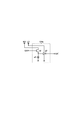
- FIG. 2 is a circuit diagram showing a configuration example of the load drive circuit 11 and the abnormality detection circuit 12.
- the load drive circuit 11 depicted in the figure includes a spindle motor driver circuit 111, a thread motor driver circuit 112, a loading motor driver circuit 113, a focus actuator driver circuit 114, a tracking actuator driver circuit 115, and a tilt. It can be understood that the vicinity of a certain one-phase output stage is depicted for any of the actuator driver circuits 116.
- the abnormality detection circuit 12 includes a first overvoltage detection unit 121, a reduced voltage detection unit 122, a second overvoltage detection unit 123, and an abnormality detection signal generation unit 124.
- the first overvoltage detection signal SA becomes a normal logic level (low level (GND)) when the first power supply voltage HV is lower than the overvoltage detection voltage Vth1, and the first power supply voltage HV is higher than the overvoltage detection voltage Vth1. Sometimes it becomes the logic level (high level (HV)) at the time of abnormality.
- FIG. 5 is a circuit diagram illustrating a configuration example of the first overvoltage detection unit 121.
- the first overvoltage detection unit 121 compares the first power supply voltage HV applied to the non-inverting input terminal (+) with the overvoltage detection voltage Vth1 applied to the inverting input terminal ( ⁇ ) to detect the first overvoltage detection.
- a comparator 121a that generates the signal SA is included.
- the first power supply terminal (high potential terminal) of the comparator 121a is connected to the application terminal of the first power supply voltage HV.
- the second power supply terminal (low potential terminal) of the comparator 121a is connected to the application terminal of the ground voltage GND.
- the reduced voltage detection signal SB becomes a normal logic level (low level (GND)) when the first power supply voltage HV is higher than the reduced voltage detection voltage Vth2, and the first power supply voltage HV is higher than the reduced voltage detection voltage Vth2.
- GDD low level
- HV high level
- FIG. 6 is a circuit diagram showing an example of the configuration of the reduced voltage detection unit 122.
- the reduced voltage detection unit 122 compares the first power supply voltage HV applied to the inverting input terminal ( ⁇ ) and the reduced voltage detection voltage Vth2 applied to the non-inverting input terminal (+) to determine a reduced voltage detection signal. It includes a comparator 122a that generates SB.
- the first power supply terminal (high potential terminal) of the comparator 122a is connected to the application terminal of the first power supply voltage HV.
- the second power supply terminal (low potential terminal) of the comparator 122a is connected to the application terminal of the ground voltage GND.
- the second overvoltage detection signal SC becomes a normal logic level (low level (GND)) when the second power supply voltage LV is lower than the overvoltage detection voltage Vth3, and the second power supply voltage LV is higher than the overvoltage detection voltage Vth3. Sometimes it becomes the logic level (high level (LV)) at the time of abnormality.
- FIG. 7 is a circuit diagram showing a configuration example of the second overvoltage detection unit 123.
- the second overvoltage detection unit 123 compares the second power supply voltage LV applied to the non-inverting input terminal (+) with the overvoltage detection voltage Vth3 applied to the inverting input terminal ( ⁇ ) to detect the second overvoltage detection.
- a comparator 123a that generates the signal SC is included.
- the first power supply terminal (high potential terminal) of the comparator 123a is connected to the application terminal of the second power supply voltage LV.
- the second power supply terminal (low potential terminal) of the comparator 123a is connected to the application terminal of the ground voltage GND.
- the abnormality detection signal generation unit 124 monitors the first overvoltage detection signal SA, the reduced voltage detection signal SB, and the second overvoltage detection signal SC to generate the abnormality detection signal S1.
- the abnormality detection signal generation unit 124 includes a level shifter 124a and a logical sum calculator 124b.
- the level shifter 124a level-shifts the first overvoltage detection signal SA pulse-driven between the first power supply voltage HV and the ground voltage GND, and is pulse-driven between the second power supply voltage LV and the ground voltage GND. A first overvoltage detection signal SA ′ is generated. With the configuration having the level shifter 124a, it is not necessary to increase the withstand voltage of the logical sum calculator 124b unnecessarily.
- FIG. 8 is a circuit diagram showing a configuration example of the level shifter 124a.
- the level shifter 124a of this configuration example includes an N-channel MOS field effect transistor a1, a current source a2, and an inverter a3.
- the drain of the transistor a1 is connected to the application end of the first power supply voltage HV.
- the source of the transistor a1 is connected to the application terminal of the ground voltage GND through the current source a2.
- the gate of the transistor a1 is connected to the application end of the first overvoltage detection signal SA.
- the input terminal of the inverter a3 is connected to the source of the transistor a1.
- the output terminal of the inverter a3 is connected to the application terminal of the first overvoltage detection signal SA '.
- the first power supply terminal (high potential terminal) of the inverter a3 is connected to the application terminal of the second power supply voltage LV.
- the second power supply terminal (low potential terminal) of the inverter a3 is connected to the application terminal of the ground voltage GND.
- the logical sum calculator 124b generates an abnormality detection signal S1 by performing a logical sum operation on the first overvoltage detection signal SA ', the reduced voltage detection signal SB, and the second overvoltage detection signal SC.
- the abnormality detection signal S1 is at a high level (LV) if any one of the first overvoltage detection signal SA ′, the reduced voltage detection signal SB, and the second overvoltage detection signal SC is at a high level, and all are at a low level. If it is, it becomes a low level (GND).
- the load driving circuit 11 includes a P channel type DMOS field effect transistor PD1, an N channel type DMOS field effect transistor ND1, P channel type MOS field effect transistors P0 and P1, an N channel type MOS field effect transistor N1, and a resistor R1. And a pre-driver DRV, a buffer BUF, an inverter INV, and a corrected power supply voltage generation unit CVG.
- the source of the transistor PD1 is connected to the application end of the first power supply voltage HV (or the second power supply voltage LV).
- the drain of the transistor PD1 is connected to the output terminal of the output signal OUT.
- the gate of the transistor PD1 is connected to the predriver DRV.
- the source of the transistor ND1 is connected to the application terminal of the ground voltage GND.
- the drain of the transistor ND1 is connected to the output terminal of the output signal OUT.
- the gate of the transistor ND1 is connected to the pre-driver DRV.
- the source of the transistor P0 is connected to the application end of the first power supply voltage HV (or the second power supply voltage LV).
- the drain of the transistor P0 is connected to the power supply voltage input terminal of the pre-driver DRV.
- the gate of the transistor P0 is connected to the output terminal of the buffer BUF.
- the input end of the buffer BUF is connected to the application end of the abnormality detection signal S1.
- the first end of the resistor R1 is connected to the power supply voltage input end of the pre-driver DRV.
- a second end of the resistor R1 is connected to an application end of the ground voltage GND.
- the source of the transistor P1 is connected to the application end of the first power supply voltage HV (or the second power supply voltage LV).
- the drain of the transistor P1 is connected to the gate of the transistor PD1.
- the gate of the transistor P1 is connected to the output terminal of the inverter INV.
- the input end of the inverter INV is connected to the application end of the abnormality detection signal S1.
- the source of the transistor N1 is connected to the application terminal of the ground voltage GND.
- the drain of the transistor N1 is connected to the gate of the transistor ND1.
- the gate of the transistor N1 is connected to the application end of the abnormality detection signal S1.
- the transistors PD1 and ND1 correspond to a push-pull output circuit that receives the supply of the first power supply voltage HV (or the second power supply voltage LV) and drives the load.
- the transistor PD1 corresponds to an upper transistor connected between the application terminal of the first power supply voltage HV (or the second power supply voltage LV) and the output terminal of the output signal OUT.
- the transistor ND1 corresponds to a lower transistor connected between the application terminal of the ground voltage GND and the output terminal of the output signal OUT.
- the pre-driver DRV is one of internal circuits that operate upon receiving the supply of the first power supply voltage HV (or the second power supply voltage LV), and the drive signal for the push-pull output circuit described above based on an instruction from the microcomputer 30. This corresponds to a drive circuit that generates (gate signals of the transistors PD1 and ND1).
- the transistor P0 corresponds to a power switch that turns on / off a power supply voltage supply line to an internal circuit (such as a pre-driver DRV) according to the abnormality detection signal S1.
- the transistor P0 is turned on when the abnormality detection signal S1 is at the low level (normal logic level), and conducts the power supply voltage supply line to the internal circuit.
- the transistor P0 is turned off when the abnormality detection signal S1 is at a high level (logical level at the time of abnormality), and interrupts the power supply voltage supply line to the internal circuit.
- the transistor P1 corresponds to a first upper switch that conducts / cuts off between the gate of the transistor PD1 and the application terminal of the first power supply voltage HV (or the second power supply voltage LV) according to the abnormality detection signal S1.
- the transistor P1 is turned off when the abnormality detection signal S1 is at the low level (normal logic level), and is between the gate of the transistor PD1 and the application terminal of the first power supply voltage HV (or the second power supply voltage LV). Cut off.
- the transistor P1 is turned on when the abnormality detection signal S1 is at a high level (logic level at the time of abnormality), and the application terminal of the gate of the transistor PD1 and the first power supply voltage HV (or the second power supply voltage LV). Conduction between.
- the transistor N1 corresponds to a first lower switch that conducts / cuts off between the gate of the transistor ND1 and the application terminal of the ground voltage GND according to the abnormality detection signal S1.
- the transistor N1 is turned off when the abnormality detection signal S1 is at a low level (normal logic level), thereby blocking between the gate of the transistor ND1 and the application terminal of the ground voltage GND.
- the transistor N1 is turned on when the abnormality detection signal S1 is at a high level (logical level at the time of abnormality), and conducts between the gate of the transistor ND1 and the application terminal of the ground voltage GND.
- the resistor R1 corresponds to a pull-down resistor connected between the power supply voltage input terminal of the internal circuit and the application terminal of the ground voltage GND.
- the buffer BUF shifts the level of the abnormality detection signal S1 that is pulse-driven between the second power supply voltage LV and the ground voltage GND, so that the first power supply voltage HV (or the second power supply voltage LV) and the first correction power supply voltage are shifted.
- a gate signal G0 that is pulse-driven to HV ′ (or the second corrected power supply voltage LV ′) is generated, and this gate signal G0 is supplied to the gate of the transistor P0.
- the inverter INV shifts the level of the abnormality detection signal S1 that is pulse-driven between the second power supply voltage LV and the ground voltage GND, and further logically inverts this to thereby detect the first power supply voltage HV (or the second power supply).
- a gate signal G1 that is pulse-driven between the voltage LV) and the first corrected power supply voltage HV ′ (or the second corrected power supply voltage LV ′) is generated, and this gate signal G1 is supplied to the gate of the transistor P1.
- FIG. 9 is a circuit diagram showing a configuration example of the corrected power supply voltage generation unit CVG.
- the corrected power supply voltage generation unit CVG of this configuration example includes a P-channel MOS field effect transistor b1, an npn bipolar transistor b2, a Zener diode b3, and resistors b4 and b5.
- the source of the transistor b1 is connected to the application terminal of the first corrected power supply voltage HV ′ (or the second corrected power supply voltage LV ′), while the first power supply voltage HV (or the second power supply voltage LV) is connected via the resistor b4. Is also connected to the application terminal.
- the drain of the transistor b1 is connected to the application terminal of the ground voltage GND.
- the gate of the transistor b1 is connected to the emitter of the transistor b2, and is also connected to the application terminal of the ground voltage GND through the resistor b5.
- the collector and base of the transistor b2 are both connected to the anode of the Zener diode b3.
- the cathode of the Zener diode b3 is connected to the application terminal of the first power supply voltage HV (or the second power supply voltage LV).
- the first corrected power supply voltage HV ′ (or the second corrected power supply voltage LV ′) lower than the first power supply voltage HV (or the second power supply voltage LV) by a predetermined value ⁇ . ) Can be generated.
- the transistor P0 when the abnormality detection signal S1 becomes high level (logic level at the time of abnormality), the transistor P0 is turned off, and the power supply voltage supply line to the internal circuit including the pre-driver DRV is provided. Blocked. Therefore, even when an abnormality (overvoltage or reduced voltage) occurs in the first power supply voltage HV or the second power supply voltage LV, it is possible to prevent the internal circuit from being destroyed.
- the transistor P0 When the transistor P0 is turned off and the power supply voltage supply line to the internal circuit is cut off, the power supply voltage input terminal of the internal circuit is pulled down to the application terminal of the ground voltage GND via the resistor R1. Therefore, since the power supply voltage input terminal of the internal circuit does not become an indefinite voltage, it is possible to avoid an abnormal operation of the internal circuit.
- the power supply voltage supply line to the push-pull output circuit is turned on / off. No switch is provided.
- transistors P1 and N1 are provided as means for protecting the transistors PD1 and ND1.
- the abnormality detection signal S1 becomes a high level (logical level at the time of abnormality)
- the transistors P1 and N1 are turned on, and the gates and sources of the transistors PD1 and ND1 are short-circuited. Accordingly, since no voltage is applied between the gate and source of the transistors PD1 and ND1, the transistors PD1 and ND1 can be protected without unnecessarily increasing the gate-source breakdown voltage of the transistors PD1 and ND1. It becomes possible.
- FIG. 10 is a timing chart showing an example of the abnormality protection operation described above. In order from the top, the first power supply voltage HV, the abnormality detection signal S1, the gate voltages of the transistors P1 and N1, and the gate voltages of the transistors PD1 and ND1. And the output signal OUT is depicted.
- an electrostatic protection diode is generally connected between the application terminal of the first power supply voltage HV (or the second power supply voltage LV) and the application terminal of the ground voltage GND. Yes. Since this electrostatic protection diode does not perform a protective operation based on the abnormality detection signal S1, it is necessary to give the element itself a sufficient breakdown voltage.
- FIG. 3 is a circuit diagram showing a modification of the load driving circuit 11.
- the load driving circuit 11 may have a configuration in which analog switches SW1 and SW2 are connected to the gates of the transistors PD1 and ND1.
- the analog switch SW1 corresponds to a second upper switch that conducts / cuts off between the gate of the transistor PD1 and the pre-driver DRV according to the abnormality detection signal S1.
- the analog switch SW1 is turned on when the abnormality detection signal S1 is at a low level (normal logic level), and conducts between the gate of the transistor PD1 and the pre-driver DRV.
- the analog switch SW1 is turned off when the abnormality detection signal S1 is at a high level (logical level at the time of abnormality), and interrupts between the gate of the transistor PD1 and the pre-driver DRV.
- the gate of the transistor PD1 is more reliably connected to the first power supply voltage HV (or the second power supply voltage LV). It becomes possible to fix to.
- the analog switch SW2 corresponds to a second lower switch that conducts / cuts off between the gate of the transistor ND1 and the pre-driver DRV according to the abnormality detection signal S1.
- the analog switch SW2 is turned on when the abnormality detection signal S1 is at a low level (normal logic level), and conducts between the gate of the transistor ND1 and the pre-driver DRV.
- the analog switch SW2 is turned off when the abnormality detection signal S1 is at a high level (logical level at the time of abnormality), and disconnects between the gate of the transistor ND1 and the pre-driver DRV.
- the gate of the transistor ND1 can be more reliably fixed to the ground voltage GND when the abnormality detection signal S1 becomes a high level (logic level at the time of abnormality).
- the first overvoltage detection signal SA and the second overvoltage detection signal SC are at a high level.
- the abnormality detection signal S1 is at a high level (logical level at the time of abnormality), and the above-described abnormality protection operation (see FIG. 10). Since it works, it is possible to avoid the smoke and destruction of IC.
- a small signal element can be protected from destruction by turning off a power supply line switch, and an output element that cannot be prevented by that is for gate-off. It can protect from destruction by introducing a switch. That is, it can be said that both the gate-off switch for the countermeasure against destruction of the output element and the switch for shutting off the power supply line are important as circuit elements for realizing the protection technique.
- the reason why the power supply line connected to the output element is not interrupted is to prevent the on-resistance of the output element from apparently increasing due to the insertion of the switch.
- FIG. 11 is an external view of a desktop personal computer equipped with the optical disc playback apparatus 1.
- the desktop personal computer X of this configuration example includes a main body case X10, a liquid crystal monitor X20, a keyboard X30, and a mouse X40.
- the main body case X10 houses a central processing unit X11, a memory X12, an optical drive X13, a hard disk drive X14, and the like.
- the central processing unit X11 comprehensively controls the operation of the desktop personal computer X by executing an operating system and various application programs stored in the hard disk drive X14.
- the memory X12 is used as a work area of the central processing unit X11 (for example, an area for storing task data when executing a program).
- the optical drive X13 reads / writes the optical disc.
- Examples of the optical disk include CD [compact disc], DVD [digital versatile disc], and BD [Blu-ray disc].
- the optical drive X13 the above-described optical disc reproducing apparatus 1 can be preferably used.
- the hard disk drive X14 is one of large-capacity auxiliary storage devices that store programs and data in a nonvolatile manner using a magnetic disk sealed in a housing.
- the liquid crystal monitor X20 outputs an image based on an instruction from the central processing unit X11.
- the keyboard X30 and the mouse X40 are one of human interface devices that accept user operations.
- FIG. 4 is a circuit diagram showing a configuration example of a switching regulator IC to which the present invention can be applied.
- the switching regulator IC 40 of this configuration example is a semiconductor integrated circuit device having a P-channel MOS field effect transistor 41, a rectifying diode 42, a switch control unit 43, an overvoltage protection unit 44, and a power switch 45.
- a coil L11, a capacitor C11, and resistors R11 and R12 are connected as discrete elements forming an output stage.
- the output stage is a step-down type, but the configuration of the output stage is not limited to this, and may be a step-up type or a step-up / step-down type.
- the transistor 41 corresponds to the transistor PD1 in FIG. 2
- the rectifying diode 42 corresponds to the transistor ND1 in FIG.
- the rectifying diode 42 can be replaced with a synchronous rectifying transistor.
- the switch control unit 43 corresponds to the driver DRV (internal circuit) in FIG. 2
- the overvoltage detection unit 44 corresponds to the abnormality detection circuit 12 in FIG.
- the power switch 45 corresponds to the transistor P0 in FIG.
- an element corresponding to the transistor P1 in FIG. 2 can be provided between the gate and the source of the transistor 41.
- the configuration of the present invention can be variously modified within the scope of the present invention in addition to the above embodiment. That is, the above-described embodiment is an example in all respects and should not be considered as limiting, and the technical scope of the present invention is not the description of the above-described embodiment, but the claims. It should be understood that all modifications that come within the meaning and range of equivalents of the claims are included.
- the present invention can be used to increase the reliability of the load driving device.
- Optical disk playback device 10 Load drive device (motor driver IC) DESCRIPTION OF SYMBOLS 11 Load drive circuit 111 Spindle motor driver circuit 112 Thread motor driver circuit 113 Loading motor driver circuit 114 Focus actuator driver circuit 115 Tracking actuator driver circuit 116 Tilt actuator driver circuit 12 Abnormality detection circuit 121 1st overvoltage detection part 121a Comparator 122 Decrease voltage detection Unit 122a comparator 123 second overvoltage detection unit 123a comparator 124 abnormality detection signal generation unit 124a level shifter a1 N-channel MOS field effect transistor a2 current source a3 inverter 124b logical sum calculator 20 load (motor / actuator) 21 Spindle motor 22 Thread motor 23 Loading motor 24 Focus actuator 25 Tracking actuator 26 Tilt actuator 30 Microcomputer 40 Switching regulator IC 41 P-channel MOS field effect transistor 42 Rectifier diode 43 Switch control unit (internal circuit) 44 Overvoltage protection unit (abnormality detection circuit) 45 Power switch
Landscapes
- Engineering & Computer Science (AREA)
- Power Engineering (AREA)
- Electronic Switches (AREA)
- Dc-Dc Converters (AREA)
- Power Conversion In General (AREA)
- Semiconductor Integrated Circuits (AREA)
Abstract
Description
以下では、光ディスク再生装置に搭載されるモータドライバICに本発明を適用した場合を例に挙げて詳細な説明を行う。 <Optical disk playback device>
In the following, a detailed description will be given by taking as an example the case where the present invention is applied to a motor driver IC mounted on an optical disc reproducing apparatus.
図11は、光ディスク再生装置1を搭載したデスクトップパソコンの外観図である。本構成例のデスクトップパソコンXは、本体ケースX10と、液晶モニタX20と、キーボードX30と、マウスX40と、を有する。 <Desktop PC>
FIG. 11 is an external view of a desktop personal computer equipped with the optical
なお、上記の実施形態では、モータドライバIC10に本発明を適用した構成を例に挙げて説明を行ったが、本発明の適用対象はこれに限定されるものではなく、図4のスイッチングレギュレータICなど、負荷駆動装置全般に広く適用することが可能である。 <Other variations>
In the above embodiment, the configuration in which the present invention is applied to the
10 負荷駆動装置(モータドライバIC)
11 負荷駆動回路
111 スピンドルモータドライバ回路
112 スレッドモータドライバ回路
113 ローディングモータドライバ回路
114 フォーカスアクチュエータドライバ回路
115 トラッキングアクチュエータドライバ回路
116 チルトアクチュエータドライバ回路
12 異常検出回路
121 第1過電圧検出部
121a コンパレータ
122 減電圧検出部
122a コンパレータ
123 第2過電圧検出部
123a コンパレータ
124 異常検出信号生成部
124a レベルシフタ
a1 Nチャネル型MOS電界効果トランジスタ
a2 電流源
a3 インバータ
124b 論理和演算器
20 負荷(モータ/アクチュエータ)
21 スピンドルモータ
22 スレッドモータ
23 ローディングモータ
24 フォーカスアクチュエータ
25 トラッキングアクチュエータ
26 チルトアクチュエータ
30 マイコン
40 スイッチングレギュレータIC
41 Pチャネル型MOS電界効果トランジスタ
42 整流用ダイオード
43 スイッチ制御部(内部回路)
44 過電圧保護部(異常検出回路)
45 電源スイッチ
PD1 Pチャネル型DMOS電界効果トランジスタ
ND1 Nチャネル型DMOS電界効果トランジスタ
P0、P1 Pチャネル型MOS電界効果トランジスタ
N1 Nチャネル型MOS電界効果トランジスタ
R1 抵抗
DRV プリドライバ
BUF バッファ(レベルシフト機能付き)
INV インバータ(レベルシフト機能付き)
CVG 補正電源電圧生成部
b1 Pチャネル型MOS電界効果トランジスタ
b2 npn型バイポーラトランジスタ
b3 ツェナダイオード
b4、b5 抵抗
SW1、SW2 アナログスイッチ
L11 コイル
C11 キャパシタ
R11、R12 抵抗
X デスクトップパソコン
X10 本体ケース
X11 中央演算処理装置
X12 メモリ
X13 光学ドライブ
X14 ハードディスクドライブ
X20 液晶モニタ
X30 キーボード
X40 マウス 1 Optical
DESCRIPTION OF
21
41 P-channel MOS
44 Overvoltage protection unit (abnormality detection circuit)
45 Power switch PD1 P channel type DMOS field effect transistor ND1 N channel type DMOS field effect transistor P0, P1 P channel type MOS field effect transistor N1 N channel type MOS field effect transistor R1 Resistor DRV Pre-driver BUF Buffer (with level shift function)
INV inverter (with level shift function)
CVG correction power supply voltage generation unit b1 P channel type MOS field effect transistor b2 npn type bipolar transistor b3 Zener diode b4, b5 resistance SW1, SW2 Analog switch L11 coil C11 capacitor R11, R12 resistance X desktop personal computer X10 main unit case X11 central processing unit X12 Memory X13 Optical drive X14 Hard disk drive X20 LCD monitor X30 Keyboard X40 Mouse
Claims (22)
- 電源電圧の供給を受けて動作する内部回路と、
前記電源電圧の供給を受けて負荷を駆動する出力回路と、
前記電源電圧を監視して異常検出信号を生成する異常検出回路と、
前記異常検出信号に応じて前記内部回路への電源電圧供給ラインを導通/遮断する電源スイッチと、
を有することを特徴とする負荷駆動装置。 An internal circuit that operates upon receipt of a power supply voltage;
An output circuit for driving a load upon receiving the supply voltage;
An abnormality detection circuit that monitors the power supply voltage and generates an abnormality detection signal;
A power switch for conducting / interrupting a power supply voltage supply line to the internal circuit in response to the abnormality detection signal;
A load driving device comprising: - 前記内部回路は、前記出力回路に駆動信号を供給する駆動回路を含むことを特徴とする請求項1に記載の負荷駆動装置。 The load driving device according to claim 1, wherein the internal circuit includes a drive circuit that supplies a drive signal to the output circuit.
- 前記内部回路の電源電圧入力端と接地端との間に接続されたプルダウン抵抗を有することを特徴とする請求項2に記載の負荷駆動装置。 The load driving device according to claim 2, further comprising a pull-down resistor connected between a power supply voltage input terminal and a ground terminal of the internal circuit.
- 前記出力回路は、電源端と出力端との間に接続されたP型の上側トランジスタを含むことを特徴とする請求項3に記載の負荷駆動装置。 4. The load driving device according to claim 3, wherein the output circuit includes a P-type upper transistor connected between a power supply terminal and an output terminal.
- 前記異常検出信号に応じて前記上側トランジスタのゲートと前記電源端との間を導通/遮断する第1上側スイッチを有することを特徴とする請求項4に記載の負荷駆動装置。 5. The load driving device according to claim 4, further comprising a first upper switch that conducts / cuts off between the gate of the upper transistor and the power supply terminal according to the abnormality detection signal.
- 前記異常検出信号に応じて前記上側トランジスタのゲートと前記駆動回路との間を導通/遮断する第2上側スイッチを有することを特徴とする請求項5に記載の負荷駆動装置。 6. The load driving device according to claim 5, further comprising a second upper switch for conducting / cutting off between the gate of the upper transistor and the driving circuit in accordance with the abnormality detection signal.
- 前記出力回路は、前記接地端と前記出力端との間に接続されたN型の下側トランジスタを含むことを特徴とする請求項4~請求項6のいずれか一項に記載の負荷駆動装置。 7. The load driving apparatus according to claim 4, wherein the output circuit includes an N-type lower transistor connected between the ground terminal and the output terminal. .
- 前記異常検出信号に応じて前記下側トランジスタのゲートと前記接地端との間を導通/遮断する第1下側スイッチを有することを特徴とする請求項7に記載の負荷駆動装置。 The load driving device according to claim 7, further comprising a first lower switch that conducts / cuts off between the gate of the lower transistor and the ground terminal in accordance with the abnormality detection signal.
- 前記異常検出信号に応じて前記下側トランジスタのゲートと前記駆動回路との間を導通/遮断する第2下側スイッチを有することを特徴とする請求項8に記載の負荷駆動装置。 9. The load driving device according to claim 8, further comprising a second lower switch that conducts / cuts off between the gate of the lower transistor and the driving circuit in accordance with the abnormality detection signal.
- 前記内部回路として、第1電源電圧を受けて動作する第1内部回路と、前記第1電源電圧よりも低い第2電源電圧を受けて動作する第2内部回路と、を有し、
前記出力回路として、前記第1電源電圧を受けて第1負荷を駆動する第1出力回路と、前記第2電源電圧を受けて第2負荷を駆動する第2出力回路と、を有することを特徴とする請求項1~請求項9のいずれか一項に記載の負荷駆動装置。 The internal circuit includes a first internal circuit that operates in response to a first power supply voltage, and a second internal circuit that operates in response to a second power supply voltage lower than the first power supply voltage,
The output circuit includes a first output circuit that receives the first power supply voltage and drives a first load, and a second output circuit that receives the second power supply voltage and drives a second load. The load driving apparatus according to any one of claims 1 to 9. - 前記異常検出回路は、
前記第1電源電圧を監視して第1過電圧検出信号を生成する第1過電圧検出部と、
前記第2電源電圧を監視して第2過電圧検出信号を生成する第2過電圧検出部と、
前記第1過電圧検出信号と前記第2過電圧検出信号に基づいて前記異常検出信号を生成する異常検出信号生成部と、
を含むことを特徴とする請求項10に記載の負荷駆動装置。 The abnormality detection circuit is
A first overvoltage detector that monitors the first power supply voltage and generates a first overvoltage detection signal;
A second overvoltage detector for monitoring the second power supply voltage and generating a second overvoltage detection signal;
An abnormality detection signal generating unit that generates the abnormality detection signal based on the first overvoltage detection signal and the second overvoltage detection signal;
The load driving device according to claim 10, comprising: - 前記第1過電圧検出部は、前記第1電源電圧と第1過電圧検出電圧とを比較して前記第1過電圧検出信号を生成する第1コンパレータを含み、
前記第2過電圧検出部は、前記第2電源電圧と第2過電圧検出電圧とを比較して前記第2過電圧検出信号を生成する第2コンパレータを含む、
ことを特徴とする請求項11に記載の負荷駆動装置。 The first overvoltage detection unit includes a first comparator that compares the first power supply voltage and a first overvoltage detection voltage to generate the first overvoltage detection signal;
The second overvoltage detection unit includes a second comparator that compares the second power supply voltage with a second overvoltage detection voltage to generate the second overvoltage detection signal.
The load driving device according to claim 11. - 前記第1過電圧検出信号の信号レベルを調整して前記異常検出信号生成部に供給する第1レベルシフタを有することを特徴とする請求項11または請求項12に記載の負荷駆動装置。 13. The load driving device according to claim 11, further comprising a first level shifter that adjusts a signal level of the first overvoltage detection signal and supplies the first overvoltage detection signal to the abnormality detection signal generation unit.
- 前記第1レベルシフタは、
ドレインが前記第1電源電圧の印加端に接続され、ゲートが前記第1過電圧検出信号の印加端に接続されたトランジスタと、
前記トランジスタのソースと接地端との間に接続された電流源と、
入力端が前記トランジスタのソースに接続され、出力端が前記異常検出信号生成部に接続され、第1電源端が前記第2電源電圧の印加端に接続され、第2電源端が接地端に接続されたインバータと、
を含むことを特徴とする請求項13に記載の負荷駆動装置。 The first level shifter is:
A transistor having a drain connected to an application terminal of the first power supply voltage and a gate connected to an application terminal of the first overvoltage detection signal;
A current source connected between a source of the transistor and a ground terminal;
An input terminal is connected to the source of the transistor, an output terminal is connected to the abnormality detection signal generator, a first power supply terminal is connected to the application terminal of the second power supply voltage, and a second power supply terminal is connected to the ground terminal An inverter,
The load driving device according to claim 13, comprising: - 前記異常検出回路は、さらに、前記第1電源電圧を監視して減電圧検出信号を生成する減電圧検出部を含み、
前記異常検出信号生成部は、前記第1過電圧検出信号、前記第2過電圧検出信号、及び前記減電圧検出信号に基づいて前記異常検出信号を生成することを特徴とする請求項11~請求項14のいずれか一項に記載の負荷駆動装置。 The abnormality detection circuit further includes a reduced voltage detection unit that monitors the first power supply voltage and generates a reduced voltage detection signal,
The abnormality detection signal generation unit generates the abnormality detection signal based on the first overvoltage detection signal, the second overvoltage detection signal, and the reduced voltage detection signal. The load driving device according to any one of the above. - 前記減電圧検出部は、前記第1電源電圧と減電圧検出電圧とを比較して前記減電圧検出信号を生成する第3コンパレータを含むことを特徴とする請求項15に記載の負荷駆動装置。 16. The load driving device according to claim 15, wherein the reduced voltage detection unit includes a third comparator that compares the first power supply voltage and a reduced voltage detection voltage to generate the reduced voltage detection signal.
- 前記異常検出信号の信号レベルを調整する第2レベルシフタを有することを特徴とする請求項1~請求項16にいずれか一項に記載の負荷駆動装置。 The load driving device according to any one of claims 1 to 16, further comprising a second level shifter that adjusts a signal level of the abnormality detection signal.
- 前記第2レベルシフタは、前記異常検出信号の信号レベルを、前記第2電源電圧と接地電圧との間でパルス駆動される状態から、前記第1電源電圧と前記第1電源電圧よりも所定値だけ低い第1補正電源電圧との間でパルス駆動される状態、または、前記第2電源電圧と前記第2電源電圧よりも所定値だけ低い第2補正電源電圧との間でパルス駆動される状態に調整することを特徴とする請求項17に記載の負荷駆動装置。 The second level shifter is configured to pulse the signal level of the abnormality detection signal between the second power supply voltage and the ground voltage by a predetermined value from the first power supply voltage and the first power supply voltage. In a state of being pulse-driven between a low first correction power supply voltage or in a state of being pulse-driven between the second power supply voltage and a second correction power supply voltage that is lower than the second power supply voltage by a predetermined value. The load driving device according to claim 17, wherein the load driving device is adjusted.
- 前記第1電源電圧または前記第2電源電圧から前記第1補正電源電圧または前記第2補正電源電圧を生成して前記第2レベルシフタに供給する補正電源電圧生成部を有することを特徴とする請求項18に記載の負荷駆動装置。 The correction power supply voltage generation part which generates the 1st correction power supply voltage or the 2nd correction power supply voltage from the 1st power supply voltage or the 2nd power supply voltage, and supplies it to the 2nd level shifter. The load driving device according to claim 18.
- 前記補正電源電圧生成部は、
ソースが前記第1補正電源電圧または前記第2補正電源電圧の印加端に接続され、ドレインが接地端に接続された第1トランジスタと、
エミッタが前記第1トランジスタのゲートに接続された第2トランジスタと、
アノードが前記第2トランジスタのベース及びコレクタに接続され、カソードが前記第1電源電圧または前記第2電源電圧の印加端に接続されたツェナダイオードと、
前記第1トランジスタのソースと前記第1電源電圧または前記第2電源電圧の印加端との間に接続された第1抵抗と、
前記第2トランジスタのエミッタと接地端との間に接続された第2抵抗と、
を含むことを特徴とする請求項19に記載の負荷駆動装置。 The corrected power supply voltage generator is
A first transistor having a source connected to an application terminal of the first correction power supply voltage or the second correction power supply voltage and a drain connected to a ground terminal;
A second transistor having an emitter connected to the gate of the first transistor;
A Zener diode having an anode connected to a base and a collector of the second transistor and a cathode connected to the application terminal of the first power supply voltage or the second power supply voltage;
A first resistor connected between a source of the first transistor and an application terminal of the first power supply voltage or the second power supply voltage;
A second resistor connected between the emitter of the second transistor and a ground terminal;
The load driving device according to claim 19, comprising: - 請求項1~請求項20のいずれか一項に記載の負荷駆動装置と、前記負荷駆動装置によって駆動される負荷と、を有することを特徴とする電子機器。 An electronic apparatus comprising: the load driving device according to any one of claims 1 to 20; and a load driven by the load driving device.
- 前記電子機器は、コンピュータに搭載されて光ディスクの再生または記録/再生を行う光ディスク再生装置であり、前記負荷は、スピンドルモータ、スレッドモータ、ローディングモータ、フォーカスアクチュエータ、トラッキングアクチュエータ、及び、チルトアクチュエータの少なくとも一つであることを特徴とする請求項21に記載の電子機器。 The electronic device is an optical disk reproducing device that is mounted on a computer and reproduces or records / reproduces an optical disk, and the load includes at least a spindle motor, a thread motor, a loading motor, a focus actuator, a tracking actuator, and a tilt actuator. The electronic apparatus according to claim 21, wherein the number is one.
Priority Applications (4)
| Application Number | Priority Date | Filing Date | Title |
|---|---|---|---|
| US14/122,292 US9509208B2 (en) | 2011-05-27 | 2012-05-25 | Load driving device and electronic device using same |
| KR1020137031346A KR101545803B1 (en) | 2011-05-27 | 2012-05-25 | Load driving device and electronic device using same |
| CN201280026175.9A CN103563227B (en) | 2011-05-27 | 2012-05-25 | Load drive device and the electronic equipment using the load drive device |
| JP2013518053A JP5740471B2 (en) | 2011-05-27 | 2012-05-25 | LOAD DRIVE DEVICE AND ELECTRONIC DEVICE USING THE SAME |
Applications Claiming Priority (2)
| Application Number | Priority Date | Filing Date | Title |
|---|---|---|---|
| JP2011119207 | 2011-05-27 | ||
| JP2011-119207 | 2011-05-27 |
Publications (1)
| Publication Number | Publication Date |
|---|---|
| WO2012165328A1 true WO2012165328A1 (en) | 2012-12-06 |
Family
ID=47259185
Family Applications (1)
| Application Number | Title | Priority Date | Filing Date |
|---|---|---|---|
| PCT/JP2012/063471 WO2012165328A1 (en) | 2011-05-27 | 2012-05-25 | Load driving device and electronic device using same |
Country Status (6)
| Country | Link |
|---|---|
| US (1) | US9509208B2 (en) |
| JP (1) | JP5740471B2 (en) |
| KR (1) | KR101545803B1 (en) |
| CN (1) | CN103563227B (en) |
| TW (1) | TWI591626B (en) |
| WO (1) | WO2012165328A1 (en) |
Families Citing this family (7)
| Publication number | Priority date | Publication date | Assignee | Title |
|---|---|---|---|---|
| JP6031871B2 (en) * | 2012-07-25 | 2016-11-24 | 富士通株式会社 | DCDC converter |
| CN104300569B (en) * | 2014-09-29 | 2016-04-20 | 华中科技大学 | HVDC dc-side short-circuit fault based on mixed type MMC passes through and restoration methods |
| US9866108B2 (en) * | 2014-10-08 | 2018-01-09 | Power Intergrations, Inc. | PFC shutdown circuit for light load |
| US10209279B2 (en) | 2015-06-24 | 2019-02-19 | Allegro Microsystems, Llc | Methods and apparatus for monitoring a level of a regulated source |
| JP6203326B1 (en) * | 2016-04-22 | 2017-09-27 | 三菱電機株式会社 | AC rotating machine control device |
| CN111693823B (en) * | 2019-03-11 | 2024-04-16 | 张民基 | Withstand voltage testing arrangement |
| CN112630513B (en) * | 2020-12-09 | 2023-10-27 | 北方工业大学 | Boost capacitor voltage detection circuit |
Citations (4)
| Publication number | Priority date | Publication date | Assignee | Title |
|---|---|---|---|---|
| JPH01318553A (en) * | 1988-06-17 | 1989-12-25 | Murata Mfg Co Ltd | Switching power circuit |
| JPH0698532A (en) * | 1992-09-14 | 1994-04-08 | Matsushita Electric Works Ltd | Power supply device |
| JP2005033862A (en) * | 2003-07-08 | 2005-02-03 | Rohm Co Ltd | Step up/down dc-dc converter and portable apparatus employing it |
| JP2008263733A (en) * | 2007-04-12 | 2008-10-30 | Rohm Co Ltd | Motor driving device, lock protection method, and cooling device using motor driving device |
Family Cites Families (15)
| Publication number | Priority date | Publication date | Assignee | Title |
|---|---|---|---|---|
| CN1254791C (en) | 2003-04-22 | 2006-05-03 | 明基电通股份有限公司 | Optical disc device capable of preventing optical head from burnning out and protection circuit |
| JP4052998B2 (en) * | 2003-11-25 | 2008-02-27 | シャープ株式会社 | Power supply circuit and electronic device using the same |
| JP2007306637A (en) * | 2006-05-08 | 2007-11-22 | Rohm Co Ltd | Load driving unit and electric apparatus using same |
| WO2007139012A1 (en) | 2006-05-30 | 2007-12-06 | Panasonic Corporation | Optical head carrying device, integrated circuit for optical head carrying device, focusing lens driving device and integrated circuit for focusing lens driving device |
| JP2008306788A (en) * | 2007-06-05 | 2008-12-18 | Ricoh Co Ltd | Switching regulator and its operation control method |
| JP4806393B2 (en) | 2007-12-14 | 2011-11-02 | オンセミコンダクター・トレーディング・リミテッド | Drive signal generation circuit |
| JP2009254170A (en) * | 2008-04-08 | 2009-10-29 | Hitachi-Lg Data Storage Inc | Motor drive circuit |
| CN202818097U (en) * | 2009-05-19 | 2013-03-20 | 罗姆股份有限公司 | Power supply apparatus and electronic device with the power supply apparatus |
| JP5363879B2 (en) * | 2009-06-03 | 2013-12-11 | ルネサスエレクトロニクス株式会社 | Driver circuit |
| JP5618733B2 (en) * | 2009-12-09 | 2014-11-05 | ローム株式会社 | Semiconductor device and switching regulator using the same |
| US8665571B2 (en) * | 2011-05-18 | 2014-03-04 | Analog Devices, Inc. | Apparatus and method for integrated circuit protection |
| JP2012213250A (en) * | 2011-03-30 | 2012-11-01 | Semiconductor Components Industries Llc | Protection circuit and input/output circuit |
| US9520767B2 (en) * | 2011-09-13 | 2016-12-13 | Fairchild (Taiwan) Corporation | Protection circuit for power converter |
| US8917076B2 (en) * | 2012-08-10 | 2014-12-23 | Monolithic Power Systems, Inc. | Off-line regulator with pass device and associated method |
| US9054517B1 (en) * | 2013-03-14 | 2015-06-09 | S3C, Inc. | Smart diagnosis and protection circuits for ASIC wiring fault conditions |
-
2012
- 2012-05-25 KR KR1020137031346A patent/KR101545803B1/en active IP Right Grant
- 2012-05-25 JP JP2013518053A patent/JP5740471B2/en active Active
- 2012-05-25 WO PCT/JP2012/063471 patent/WO2012165328A1/en active Application Filing
- 2012-05-25 US US14/122,292 patent/US9509208B2/en active Active
- 2012-05-25 TW TW101118834A patent/TWI591626B/en active
- 2012-05-25 CN CN201280026175.9A patent/CN103563227B/en active Active
Patent Citations (4)
| Publication number | Priority date | Publication date | Assignee | Title |
|---|---|---|---|---|
| JPH01318553A (en) * | 1988-06-17 | 1989-12-25 | Murata Mfg Co Ltd | Switching power circuit |
| JPH0698532A (en) * | 1992-09-14 | 1994-04-08 | Matsushita Electric Works Ltd | Power supply device |
| JP2005033862A (en) * | 2003-07-08 | 2005-02-03 | Rohm Co Ltd | Step up/down dc-dc converter and portable apparatus employing it |
| JP2008263733A (en) * | 2007-04-12 | 2008-10-30 | Rohm Co Ltd | Motor driving device, lock protection method, and cooling device using motor driving device |
Also Published As
| Publication number | Publication date |
|---|---|
| TWI591626B (en) | 2017-07-11 |
| US20140084835A1 (en) | 2014-03-27 |
| CN103563227A (en) | 2014-02-05 |
| JPWO2012165328A1 (en) | 2015-02-23 |
| KR101545803B1 (en) | 2015-08-19 |
| TW201303855A (en) | 2013-01-16 |
| US9509208B2 (en) | 2016-11-29 |
| KR20140004790A (en) | 2014-01-13 |
| CN103563227B (en) | 2017-06-09 |
| JP5740471B2 (en) | 2015-06-24 |
Similar Documents
| Publication | Publication Date | Title |
|---|---|---|
| JP5740471B2 (en) | LOAD DRIVE DEVICE AND ELECTRONIC DEVICE USING THE SAME | |
| US11217989B2 (en) | Drive device, power supply system, and method of testing drive device | |
| US7839610B2 (en) | Load driving device and electrical device using the same | |
| US8330406B2 (en) | Motor drive circuit | |
| JP6344956B2 (en) | Power circuit | |
| US20130188287A1 (en) | Protection circuit, charge control circuit, and reverse current prevention method employing charge control circuit | |
| US20140300993A1 (en) | Motor drive device, magnetic disk storage device, and electronic appliance | |
| US9025266B2 (en) | Semiconductor integrated circuit device, magnetic disk storage device, and electronic apparatus | |
| US20140300987A1 (en) | Motor drive device, magnetic disk storage device, and electronic device | |
| US9142248B2 (en) | Motor drive device, magnetic disk storage device, and electronic device | |
| JP2017079398A (en) | Electronic control device | |
| JP5279252B2 (en) | Switch output circuit | |
| JP4863660B2 (en) | Semiconductor integrated circuit device | |
| US20130258515A1 (en) | Motor drive device, magnetic disk storage device, and electronic appliance | |
| JP2011100499A (en) | Hard disk device control circuit and hard disk device | |
| US8982498B2 (en) | Switching regulator, motor drive device, magnetic disk storage device, and electronic apparatus | |
| JP6216171B2 (en) | Power circuit | |
| US8982497B2 (en) | Class-AB amplifier, motor drive device, magnetic disk storage device, and electronic apparatus | |
| JP2012100405A (en) | Load drive device and disk reproduction device using the same | |
| JP6017822B2 (en) | Overcurrent protection circuit, load drive device, optical disk device, car audio equipment | |
| JP6072585B2 (en) | Semiconductor device | |
| JP7168105B2 (en) | switching control circuit, semiconductor device | |
| JP2012080488A (en) | Gate drive circuit | |
| JP5152958B2 (en) | Semiconductor integrated circuit device |
Legal Events
| Date | Code | Title | Description |
|---|---|---|---|
| 121 | Ep: the epo has been informed by wipo that ep was designated in this application |
Ref document number: 12793144 Country of ref document: EP Kind code of ref document: A1 |
|
| ENP | Entry into the national phase |
Ref document number: 2013518053 Country of ref document: JP Kind code of ref document: A |
|
| ENP | Entry into the national phase |
Ref document number: 20137031346 Country of ref document: KR Kind code of ref document: A |
|
| WWE | Wipo information: entry into national phase |
Ref document number: 14122292 Country of ref document: US |
|
| NENP | Non-entry into the national phase |
Ref country code: DE |
|
| 122 | Ep: pct application non-entry in european phase |
Ref document number: 12793144 Country of ref document: EP Kind code of ref document: A1 |