JP4052998B2 - Power supply circuit and electronic device using the same - Google Patents
Power supply circuit and electronic device using the same Download PDFInfo
- Publication number
- JP4052998B2 JP4052998B2 JP2003393340A JP2003393340A JP4052998B2 JP 4052998 B2 JP4052998 B2 JP 4052998B2 JP 2003393340 A JP2003393340 A JP 2003393340A JP 2003393340 A JP2003393340 A JP 2003393340A JP 4052998 B2 JP4052998 B2 JP 4052998B2
- Authority
- JP
- Japan
- Prior art keywords
- circuit
- voltage
- output
- output voltage
- power supply
- Prior art date
- Legal status (The legal status is an assumption and is not a legal conclusion. Google has not performed a legal analysis and makes no representation as to the accuracy of the status listed.)
- Expired - Fee Related
Links
Images


Classifications
-
- H—ELECTRICITY
- H02—GENERATION; CONVERSION OR DISTRIBUTION OF ELECTRIC POWER
- H02M—APPARATUS FOR CONVERSION BETWEEN AC AND AC, BETWEEN AC AND DC, OR BETWEEN DC AND DC, AND FOR USE WITH MAINS OR SIMILAR POWER SUPPLY SYSTEMS; CONVERSION OF DC OR AC INPUT POWER INTO SURGE OUTPUT POWER; CONTROL OR REGULATION THEREOF
- H02M3/00—Conversion of dc power input into dc power output
- H02M3/02—Conversion of dc power input into dc power output without intermediate conversion into ac
- H02M3/04—Conversion of dc power input into dc power output without intermediate conversion into ac by static converters
- H02M3/10—Conversion of dc power input into dc power output without intermediate conversion into ac by static converters using discharge tubes with control electrode or semiconductor devices with control electrode
- H02M3/145—Conversion of dc power input into dc power output without intermediate conversion into ac by static converters using discharge tubes with control electrode or semiconductor devices with control electrode using devices of a triode or transistor type requiring continuous application of a control signal
- H02M3/155—Conversion of dc power input into dc power output without intermediate conversion into ac by static converters using discharge tubes with control electrode or semiconductor devices with control electrode using devices of a triode or transistor type requiring continuous application of a control signal using semiconductor devices only
- H02M3/156—Conversion of dc power input into dc power output without intermediate conversion into ac by static converters using discharge tubes with control electrode or semiconductor devices with control electrode using devices of a triode or transistor type requiring continuous application of a control signal using semiconductor devices only with automatic control of output voltage or current, e.g. switching regulators
-
- H—ELECTRICITY
- H05—ELECTRIC TECHNIQUES NOT OTHERWISE PROVIDED FOR
- H05B—ELECTRIC HEATING; ELECTRIC LIGHT SOURCES NOT OTHERWISE PROVIDED FOR; CIRCUIT ARRANGEMENTS FOR ELECTRIC LIGHT SOURCES, IN GENERAL
- H05B45/00—Circuit arrangements for operating light-emitting diodes [LED]
- H05B45/30—Driver circuits
- H05B45/37—Converter circuits
- H05B45/3725—Switched mode power supply [SMPS]
- H05B45/38—Switched mode power supply [SMPS] using boost topology
-
- H—ELECTRICITY
- H02—GENERATION; CONVERSION OR DISTRIBUTION OF ELECTRIC POWER
- H02M—APPARATUS FOR CONVERSION BETWEEN AC AND AC, BETWEEN AC AND DC, OR BETWEEN DC AND DC, AND FOR USE WITH MAINS OR SIMILAR POWER SUPPLY SYSTEMS; CONVERSION OF DC OR AC INPUT POWER INTO SURGE OUTPUT POWER; CONTROL OR REGULATION THEREOF
- H02M1/00—Details of apparatus for conversion
- H02M1/36—Means for starting or stopping converters
-
- Y—GENERAL TAGGING OF NEW TECHNOLOGICAL DEVELOPMENTS; GENERAL TAGGING OF CROSS-SECTIONAL TECHNOLOGIES SPANNING OVER SEVERAL SECTIONS OF THE IPC; TECHNICAL SUBJECTS COVERED BY FORMER USPC CROSS-REFERENCE ART COLLECTIONS [XRACs] AND DIGESTS
- Y02—TECHNOLOGIES OR APPLICATIONS FOR MITIGATION OR ADAPTATION AGAINST CLIMATE CHANGE
- Y02B—CLIMATE CHANGE MITIGATION TECHNOLOGIES RELATED TO BUILDINGS, e.g. HOUSING, HOUSE APPLIANCES OR RELATED END-USER APPLICATIONS
- Y02B20/00—Energy efficient lighting technologies, e.g. halogen lamps or gas discharge lamps
- Y02B20/30—Semiconductor lamps, e.g. solid state lamps [SSL] light emitting diodes [LED] or organic LED [OLED]
-
- Y—GENERAL TAGGING OF NEW TECHNOLOGICAL DEVELOPMENTS; GENERAL TAGGING OF CROSS-SECTIONAL TECHNOLOGIES SPANNING OVER SEVERAL SECTIONS OF THE IPC; TECHNICAL SUBJECTS COVERED BY FORMER USPC CROSS-REFERENCE ART COLLECTIONS [XRACs] AND DIGESTS
- Y10—TECHNICAL SUBJECTS COVERED BY FORMER USPC
- Y10S—TECHNICAL SUBJECTS COVERED BY FORMER USPC CROSS-REFERENCE ART COLLECTIONS [XRACs] AND DIGESTS
- Y10S323/00—Electricity: power supply or regulation systems
- Y10S323/901—Starting circuits
Landscapes
- Engineering & Computer Science (AREA)
- Power Engineering (AREA)
- Dc-Dc Converters (AREA)
- Circuit Arrangement For Electric Light Sources In General (AREA)
- Protection Of Static Devices (AREA)
Description
本発明は、直流電源からの入力電圧を昇圧して負荷へ供給する電源回路に関するものであり、特に、PWM信号に応じて昇圧動作の作動/停止が繰り返される電源回路に関するものである。 The present invention relates to a power supply circuit that boosts an input voltage from a DC power supply and supplies the boosted voltage to a load, and more particularly, to a power supply circuit in which a boosting operation is repeatedly activated / stopped according to a PWM signal.
近年、携帯電話機、PDA(Personal Digital Assistants)、デジタルカメラ等の電子機器に搭載されている液晶表示装置(LCD)の照明源(バックライトまたはフロントライト)のひとつとして、耐久性、発光効率、占有面積等の点で優れている白色発光ダイオードが用いられるようになってきている。この白色発光ダイオードは比較的高い順方向電圧が必要であることや、通常、照明源としては複数の白色発光ダイオードが用いられ、用いられる複数の白色発光ダイオードは各白色発光ダイオードの輝度を均一にするために直列接続されることなどから、このような照明源としての白色発光ダイオードの駆動には、携帯機器に内臓されている電池からの直流電圧よりも高い直流電圧が必要となる。 In recent years, as one of the illumination sources (backlights or frontlights) of liquid crystal display devices (LCD) installed in electronic devices such as mobile phones, PDAs (Personal Digital Assistants), digital cameras, durability, luminous efficiency, and occupation White light emitting diodes that are superior in terms of area and the like have been used. This white light emitting diode requires a relatively high forward voltage, and usually, a plurality of white light emitting diodes are used as an illumination source, and the plurality of white light emitting diodes used have uniform brightness of each white light emitting diode. Therefore, in order to drive the white light emitting diode as such an illumination source, a DC voltage higher than the DC voltage from the battery built in the portable device is required.
そこで、このような白色発光ダイオードを駆動する回路として、従来より、図9に示す昇圧型の電源回路が用いられている。図9は従来の電源回路の電気的構成を示す回路ブロック図である。図9に示す電源回路は、リチウムイオン電池等の直流電源1、入力コンデンサ2、コイル3、ダイオード(整流素子)4、出力コンデンサ5、抵抗(出力電流検出抵抗)R1、及び、1つのパッケージにIC化されコイル3に対するエネルギーの蓄積/放出を切り換えて昇圧動作を行う昇圧チョッパレギュレータ10から構成されており、携帯電話機等の電子機器に搭載されているLCDの照明源である6個の白色発光ダイオード(負荷)LED1〜6を駆動する。
Therefore, as a circuit for driving such a white light emitting diode, a boost type power supply circuit shown in FIG. 9 has been conventionally used. FIG. 9 is a circuit block diagram showing an electrical configuration of a conventional power supply circuit. The power supply circuit shown in FIG. 9 includes a
直流電源1の負極端子はグランドに接続され、正極端子は入力コンデンサ2を介してグランドに接続されるとともにコイル3の一端に接続されている。そして、コイル3の他端はダイオード4のアノードに接続され、ダイオード4のカソードは出力コンデンサ5を介してグランドに接続されている。また、出力コンデンサ5と並列に、白色発光ダイオードLED1〜6、及び抵抗R1が直列に接続された直列回路が接続されている。
The negative terminal of the
また、昇圧チョッパレギュレータ10は、外部接続用の端子として電源端子Vi、電源端子GND、出力電圧モニタ端子Vo、フィードバック端子FB、コントロール端子CTRLを備えている。そして、電源端子Viは直流電源1の正極端子に接続され、電源端子GNDはグランドに接続されており、これにより、昇圧チョッパレギュレータ10は直流電源1をその動作電源として得ている。また、スイッチ端子Vswはコイル3とダイオード4との接続点に接続され、出力電圧モニタ端子Voはダイオード4のカソードに接続され、フィードバック端子FBは白色発光ダイオードLED6と抵抗R1との接続点に接続されている。また、コントロール端子CTRLには、後述する白色発光ダイオードLED1〜6の輝度を調整するための輝度調整信号(外部入力信号)が入力される。
Further, the
次に、昇圧チョッパレギュレータ10の内部構成とその接続を説明する。昇圧チョッパレギュレータ10は、Nチャンネル型のFET(スイッチング素子)11、12、ドライブ回路13、電流検出コンパレータ14、発振回路15、アンプ16、PWMコンパレータ17、エラーアンプ18、基準電源19、抵抗R2、R3、R4、ソフトスタート回路20、ON/OFF回路(作動/停止回路)21、過熱保護回路22、過電圧保護回路23から構成されている。
Next, the internal configuration of the
FET11、12の互いのドレインはともにスイッチ端子Vswに接続され、互いのゲートはともにドライブ回路13に接続されている。そして、FET12のソースはグランドに接続され、FET11のソースは抵抗R2を介してグランドに接続されている。そして、抵抗R2の両端は電流検出コンパレータ14の2つの入力端子にそれぞれ接続され、電流検出コンパレータ14の出力と発振回路15の2つの出力の一方の出力とがアンプ16で加算されてPWMコンパレータ17に一方の入力として供給される。また、PWMコンパレータ17の出力と、発振回路15のもう一方の出力とがドライブ回路13にそれぞれ供給される。
The drains of the
また、PWMコンパレータ17の他方の入力端子にはエラーアンプ18の出力が供給され、エラーアンプ18の一方の入力端子はフィードバック端子FBに接続されている。また、エラーアンプ18の他方の入力端子は抵抗R3、R4の一端に接続され、抵抗R4の他端はグランドに接続され、抵抗R3の他端は基準電源19の正極端子に接続されている。そして、基準電源19の負極端子はグランドに接続されている。
The output of the
また、ソフトスタート回路20、ON/OFF回路21、過熱保護回路22、過電圧保護回路23の出力はドライブ回路13にそれぞれ供給され、ソフトスタート回路20、ON/OFF回路21には、コントロール端子CTRLを介して輝度調整信号が供給される。そして、過電圧保護回路23には、出力電圧モニタ端子Voを介して出力電圧Voutが供給される。
The outputs of the
次に、このような構成の図9に示す電源回路の動作を説明する。図9に示す電源回路は、ドライブ回路13がFET12をオン/オフすることにより、直流電源1からの入力電圧Vinを昇圧した出力電圧Voutを出力コンデンサ5の両端に発生させる。即ち、ドライブ回路13がFET12のゲートに所定のゲート電圧を印加しFET12がオンしているときには、直流電源1からの電流がコイル3に流れ、コイル3にエネルギーが蓄積される。そして、ドライブ回路13がFET12のゲートに所定のゲート電圧を印加せずFET12がオフしているときには、蓄積されたエネルギーが放出されることによってコイル3に逆起電力が発生する。
Next, the operation of the power supply circuit having the above configuration shown in FIG. 9 will be described. The power supply circuit shown in FIG. 9 generates an output voltage Vout obtained by boosting the input voltage Vin from the
コイル3に発生した逆起電力は直流電源1の入力電圧Vinに加算され、ダイオード4を介して出力コンデンサ5を充電する。そして、このような一連の動作を繰り返すことにより昇圧動作が行われ、出力コンデンサ5の両端に出力電圧Voutが発生し、この出力電圧Voutによって白色発光ダイオードLED1〜6に出力電流Ioutが流れ、白色発光ダイオードLED1〜6が発光する。
The back electromotive force generated in the
そして、この出力電流Ioutの電流値に抵抗R1の抵抗値を乗じたフィードバック電圧Vfbがフィードバック端子FBを介してエラーアンプ18の一方の入力端子に供給され、エラーアンプ18の他方の入力端子に供給される基準電圧Vrefと比較される。尚、この基準電圧Vrefは基準電源19の電圧を抵抗R3、R4で分圧した電圧である。このため、エラーアンプ18の出力にはフィードバック電圧Vfbと基準電圧Vrefとの差異に対応した電圧が現れ、この電圧がPWMコンパレータ17の一方の入力端子に供給される。
Then, a feedback voltage Vfb obtained by multiplying the current value of the output current Iout by the resistance value of the resistor R1 is supplied to one input terminal of the
また、PWMコンパレータ17の他方の入力端子に入力される信号は、FET11がオンすることによって抵抗R2を流れる電流に比例する信号と、発振回路15からの鋸歯状波信号とをアンプ16で加算し増幅した信号であり、この信号がPWMコンパレータ17の前記一方の入力端子に供給されるエラーアンプ18の出力電圧レベルと比較される。その結果、エラーアンプ18からの出力電圧レベルがアンプ16からの信号レベルより高くなる期間では、PWMコンパレータ17のPWM出力はH(High)レベルになり、エラーアンプ18からの出力電圧レベルがアンプ16からの信号レベルより低くなる期間では、PWMコンパレータ17のPWM出力はL(Low)レベルになる。
Further, the signal input to the other input terminal of the
そして、ドライブ回路13はPWMコンパレータ17のPWM出力を受けて、そのPWM出力に応じたデューティでFET11、12をオン/オフする。即ち、ドライブ回路13は、PWMコンパレータ17のPWM出力がHレベルのときであって、発振回路15からのクロック信号の各サイクルの開始のときに、FET11、12に所定のゲート電圧を与えてFET11、12をオンさせる。そして、PWMコンパレータ17のPWM出力がLレベルになったときにFET11、12へのゲート電圧の供給を停止し、FET11、12をオフさせる。
The
このようなFET11、12のオン/オフ制御を行うと、フィードバック電圧Vfbと基準電圧Vrefとが等しくなるように昇圧動作が行われることになる。即ち、出力電流Ioutは、基準電圧Vref(=フィードバック電圧Vfb)を抵抗R1の抵抗値で除した電流値に安定化される。また、PWMコンパレータ17で比較される信号には、抵抗R2を流れる電流に応じた信号、即ち、FET11、12がオンすることによりコイル3を流れる電流に応じた信号が加算されていることから、コイル3に流れるピーク電流を制限している。
When such on / off control of the
また、過電圧保護回路23は、出力電圧Voutが所定の過電圧保護電圧を超えたことを検知してドライブ回路13の動作を停止させるので、前記所定の過電圧保護電圧を超える過電圧が負荷である白色発光ダイオードLED1〜6や出力コンデンサ5に印加されることを防止している。また、過熱保護回路22は、ドライブ回路13の動作に伴う、特に、FET12周辺の過熱を検知してドライブ回路13の動作を停止させるので、昇圧チョッパレギュレータ10の過熱による故障や破壊を防止している。
Further, since the
また、ON/OFF回路21は、コントロール端子CTRLに入力される外部入力信号に応じてドライブ回路13のFET11、12の駆動動作を作動/停止させるものであり、コントロール端子CTRLにこの外部入力信号として、PWM(Pulse Width Modulation)信号である輝度調整信号を入力することにより白色発光ダイオードLED1〜6の輝度を調整することができる。即ち、ON/OFF回路21は、コントロール端子CTRLに入力される輝度調整信号がHレベルのときにドライブ回路13のFET11、12の駆動動作を作動させて白色発光ダイオードLED1〜6に出力電流Ioutを流し、輝度調整信号がLレベルのときにはドライブ回路13のFET11、12の駆動動作を停止させて出力電圧Voutを低下させるので、白色発光ダイオードLED1〜6に流れる平均電流は輝度調整信号のデューティに応じて変化することになる。そして、白色発光ダイオードLED1〜6の輝度はこの平均電流に比例するので、このようにして白色発光ダイオードLED1〜6の輝度が調整される。
The ON /
また、ソフトスタート回路20は、ドライブ回路13の動作開始時に、ドライブ回路13の出力デューティを徐々に変化させることにより出力電圧Voutを緩やかに上昇させるものである。出力電圧Voutを緩やかに上昇させなければ、出力コンデンサ5が充電されていない場合に、充電のための過大な充電電流が直流電源1から流れることになり、直流電源1がリチウムイオン電池等の電池である場合、電池に負担がかかるとともに、電池電圧がこの過大な充電電流により低下し、電池が本来の終止電圧まで使用できなくなるという問題が発生する。
The
図10、図11は、図9に示す電源回路の各部の電圧波形及び電流波形を示す波形図である。ここで、図10はソフトスタート回路20の効果を説明するために、ソフトスタート回路20が機能していない状態の波形を示し、図11はソフトスタート回路20が機能している状態の波形を示している。図10、図11において、(a)はコントロール端子CTRLに入力される輝度調整信号の電圧波形、(b)は出力電圧Voutの波形、(c)は入力電流Iinの波形を示している。尚、図10、図11において、最初に輝度調整信号がHレベルに変化するときが図9に示す電源回路の起動時であり、このときに直流電源1から入力電圧Vinが供給される。そして、このときまで出力電圧Voutは0Vであり、出力コンデンサ5は全く充電されていない状態である。
10 and 11 are waveform diagrams showing voltage waveforms and current waveforms of respective parts of the power supply circuit shown in FIG. Here, in order to explain the effect of the
先ず、図10を参照してソフトスタート回路20が機能していないときの昇圧動作の説明をする。図10において、起動時、即ち、最初に輝度調整信号がHレベルになったとき(図10(a))、ドライブ回路13は昇圧動作を開始するが、ソフトスタート機能は働かないので出力電圧Voutは即座に電圧V1まで上昇する(図10(b))。このとき、入力電流Iinは電圧V1で出力コンデンサ5を充電する充電電流となるため、過大な電流となる(図10(c))。
First, the boosting operation when the
尚、電圧V1とは、昇圧された出力電圧Voutにより白色発光ダイオードLED1〜6と抵抗R1とに出力電流Ioが流れ、これによりフィードバック端子FBに発生するフィードバック電圧Vfbが基準電圧Vrefと等しくなる出力電圧Voutの電圧のことである。そして、出力コンデンサ5の充電が進むにつれて入力電流Iinは減少し、その後一定となる(図10(c))。 The voltage V1 is an output in which the output current Io flows through the white light emitting diodes LED1 to LED6 and the resistor R1 by the boosted output voltage Vout, whereby the feedback voltage Vfb generated at the feedback terminal FB becomes equal to the reference voltage Vref. This is the voltage Vout. As the charging of the output capacitor 5 proceeds, the input current Iin decreases and thereafter becomes constant (FIG. 10 (c)).
次に、輝度調整信号がLレベルになると(図10(a))、ON/OFF回路21がドライブ回路13の昇圧動作を停止させるので、出力電圧Voutは直流電源1の入力電圧Vinとなり(図10(b))、入力電流Iinは流れなくなる(図10(c))。
Next, when the luminance adjustment signal becomes L level (FIG. 10A), the ON /
そして、その後、輝度調整のため輝度調整信号が所定のデューティでHレベル/Lレベルに切り換わると(図10(a))、出力電圧Voutは輝度調整信号に応じて電圧V1とVinとに切り換わる(図10(b))。出力電圧がVinからV1に切り換わるときに流れる入力電流Iinは、出力コンデンサ5が既に入力電圧Vinの電圧値に充電されているので、電圧V1から入力電圧Vinを差し引いた電圧で出力コンデンサ5を充電する充電電流となり、過大な電流とはならない(図10(c))。 After that, when the luminance adjustment signal is switched to H level / L level with a predetermined duty for luminance adjustment (FIG. 10A), the output voltage Vout is switched to the voltages V1 and Vin according to the luminance adjustment signal. It changes (FIG. 10B). The input current Iin that flows when the output voltage switches from Vin to V1 is obtained by subtracting the input voltage Vin from the voltage V1 because the output capacitor 5 is already charged to the voltage value of the input voltage Vin. It becomes a charging current for charging, and does not become an excessive current (FIG. 10C).
以上がソフトスタート回路20が機能していない状態での昇圧動作の説明であるが、起動時に流れる入力電流Vinが過大になることが問題である。即ち、起動時には出力コンデンサ5を充電する過大な充電電流が電池である直流電源1から流れ出すために、電池に負担がかかるとともに、電池電圧がこの過大な充電電流により低下し、電池が本来の終止電圧まで使用できなくなるという問題が発生する。この問題を解決するためにソフトスタート回路20が機能することが必要である。
The above is the description of the step-up operation in a state where the
次に、図11を参照してソフトスタート回路20が機能しているときの昇圧動作の説明をする。図11において、起動時、即ち、最初に輝度調整信号がHレベルになったとき(図11(a))、ドライブ回路13は昇圧動作を開始するが、ソフトスタート回路20がドライブ回路13の出力デューティを徐々に変化させるので、出力電圧Voutは入力電圧Vinの電圧に成った後、電圧V1まで緩やかに上昇する(図11(b))。起動時の入力電流Iinは入力電圧Vinで出力コンデンサ5を充電する充電電流となるため、過大な電流とはならない。(図11(c))。そして、出力コンデンサ5の充電が進むにつれて入力電流Iinは減少し、その後一定となる(図11(c))。
Next, the boosting operation when the
次に、輝度調整信号がLレベルになると(図11(a))、ON/OFF回路21がドライブ回路13の昇圧動作を停止させるので、出力電圧Voutは直流電源1の入力電圧Vinとなり(図11(b))、入力電流Iinは流れなくなる(図11(c))。
Next, when the luminance adjustment signal becomes L level (FIG. 11A), the ON /
そして、その後、輝度調整のため輝度調整信号が所定のデューティでHレベル/Lレベルに切り換わると(図11(a))、出力電圧Voutは輝度調整信号がLレベルからHレベルに切り換わるときには、ソフトスタート回路20がドライブ回路13のスイッチング動作を制御することにより電圧V1に向かって緩やかに上昇するが、輝度調整信号がHレベルからLレベルに切り換わるときに即座に電圧Vinとなる(図11(b))。出力電圧Voutが入力電圧Vinから電圧V1に向かって上昇するときに流れる入力電流Iinは、出力コンデンサ5が既に入力電圧Vinの電圧値に充電されているので、上昇した分の電圧で出力コンデンサ5を充電する充電電流となり、過大な電流とはならない(図10(c))。このように、ソフトスタート回路20が機能することにより、起動時の入力電流Vinが過大になることを防止し、直流電源1にダメージ等を与えることを防ぐことができる。
After that, when the luminance adjustment signal is switched to H level / L level with a predetermined duty for luminance adjustment (FIG. 11 (a)), the output voltage Vout is obtained when the luminance adjustment signal is switched from L level to H level. The
また、一次巻線と該一次巻線とは異なる巻き数で構成された二次巻線とを有するトランスと、直流電源の電源端子間に前記トランスの一次巻線と直列接続されたスイッチング素子と、前記直流電源の立ち上がり時にソフトスタート用コンデンサを充電し、その充電電圧に相対した電圧信号をソフト制御信号として出力するソフトスタート回路と、前記ソフトスタート回路から出力されるソフト制御信号に基づいて、前記スイッチング素子のデューティ比を徐々に高めるように制御する制御回路とを備えたスイッチング電源装置であって、前記直流電源の所定電圧値以下の立ち下がりを検出し、その検出信号を出力する電圧変動検出回路と、前記電圧変動検出回路から出力された検出信号に基づいて、前記ソフトスタート用コンデンサの充電電荷を強制的に放電させる強制放電回路とを備えたスイッチング電源装置もある。(例えば、特許文献1参照)。
しかしながら、図9に示す従来の電源回路は、図11に示すように、コントロール端子CTRLに入力される輝度調整信号がHレベルになる度、即ち、ON/OFF回路21によりドライブ回路13が昇圧動作を開始する度にソフトスタート回路20が動作して出力電圧Voutが緩やかに上昇するため、出力電圧Voutが電圧V1まで即座に立ち上がらないため、白色発光ダイオードLED1〜6に一定の出力電流Ioを流すことができず、輝度調整信号のデューティに応じた所望の輝度調整が行えないという問題があった。
However, in the conventional power supply circuit shown in FIG. 9, as shown in FIG. 11, the
また、特許文献1に記載の従来技術では、スイッチング電源装置が瞬断や短時間で再びオンされた場合でも、ソフトスタート動作を確実に行うことができ、スイッチング素子の損傷を未然に防止することはできるが、短いサイクルでオン/オフされた場合には、オンする度にソフトスタート動作で出力電圧が緩やかに立ち上がるので、出力電圧が所望の電圧まで立ち上がらない。従って、図9に示すような白色発光ダイオードを駆動するとともに輝度調整信号に応じて輝度調整を行う電源回路として使用する場合には、やはり所望の輝度調整が行えないという問題があった。
Further, in the prior art described in
本発明は、上記の点に鑑み、起動時に流れる過大な入力電流を制限するとともに、PWM信号に応じて昇圧動作の作動/停止が繰り返される場合であっても出力電圧を所望の電圧に即座に立ち上げることのできる電源回路を提供することを目的とする。 In view of the above points, the present invention limits an excessive input current that flows at the time of start-up, and immediately sets the output voltage to a desired voltage even when the boosting operation is repeatedly activated / stopped according to the PWM signal. An object is to provide a power supply circuit that can be started up.
上記目的を達成するために本発明は、直流電源の一方の端子に接続されるコイルと、一端が前記コイルに接続され他端が前記直流電源の他方の端子に接続されるスイッチング素子と、該スイッチング素子と並列に接続される整流素子と出力コンデンサとの直列回路と、前記出力コンデンサと並列に接続される負荷と出力電流検出抵抗との直列回路と、前記負荷に流れる出力電流が一定になるように前記出力電流検出抵抗からのフィードバック電圧に基づいて前記スイッチング素子を駆動するドライブ回路とを備える電源回路において、前記整流素子と出力コンデンサとの接続点に発生する出力電圧を外部から調整するために、外部入力信号に応じて前記ドライブ回路の前記スイッチング素子の駆動動作を作動/停止する作動/停止回路と、前記出力電圧が所定の電圧より高いことを検出して検出信号を出力する出力電圧検出回路と、前記外部入力信号が入力されたときに前記出力電圧検出回路からの検出信号が与えられている場合は動作せず、与えられていない場合は前記出力電圧が緩やかに上昇するように前記ドライブ回路を制御するソフトスタート回路とを設けたものである。 To achieve the above object, the present invention provides a coil connected to one terminal of a DC power supply, a switching element having one end connected to the coil and the other end connected to the other terminal of the DC power supply, A series circuit of a rectifying element and an output capacitor connected in parallel to the switching element, a series circuit of a load and an output current detection resistor connected in parallel to the output capacitor, and an output current flowing through the load are constant In a power supply circuit including a drive circuit that drives the switching element based on a feedback voltage from the output current detection resistor, the output voltage generated at the connection point between the rectifying element and the output capacitor is adjusted from the outside An operation / stop circuit for operating / stopping the driving operation of the switching element of the drive circuit in response to an external input signal; When an output voltage detection circuit that detects that the output voltage is higher than a predetermined voltage and outputs a detection signal, and when the detection signal from the output voltage detection circuit is given when the external input signal is input A soft start circuit is provided which controls the drive circuit so that the output voltage rises slowly when not operating and not applied.
このようにすると、起動時は、出力電圧が低いことを検出して前記ソフトスタート回路を動作させ、出力電圧を緩やかに上昇させることにより前記直流電源から流れる電流が過大になることを防ぎ、一旦、出力電圧が立ち上がった後は、外部入力信号に応じて前記ドライブ回路の前記スイッチング素子の駆動動作が作動/停止を繰り返す場合においても、前記ソフトスタート回路を動作させないようにすることで出力電圧を即座に立ち上げることができる。 In this way, at the time of start-up, it detects that the output voltage is low, operates the soft start circuit, and prevents the current flowing from the DC power source from becoming excessive by gradually increasing the output voltage. After the output voltage rises, the output voltage can be reduced by not operating the soft start circuit even when the drive operation of the switching element of the drive circuit repeats operation / stop in response to an external input signal. It can be launched immediately.
また、本発明は、直流電源の一方の端子に接続されるコイルと、一端が前記コイルに接続され他端が前記直流電源の他方の端子に接続されるスイッチング素子と、該スイッチング素子と並列に接続される整流素子と出力コンデンサとの直列回路と、前記出力コンデンサと並列に接続される負荷と出力電流検出抵抗との直列回路と、前記負荷に流れる出力電流が一定になるように前記出力電流検出抵抗からのフィードバック電圧に基づいて前記スイッチング素子を駆動するドライブ回路とを備える電源回路において、前記整流素子と出力コンデンサとの接続点に発生する出力電圧を外部から調整するために、外部入力信号に応じて前記ドライブ回路の前記スイッチング素子の駆動動作を作動/停止する作動/停止回路と、前記出力電圧が第1の所定電圧より高いことを検出して検出信号を出力するとともに、前記出力電圧が第2の所定電圧より低くなるときに前記検出信号の出力を停止する出力電圧検出回路と、前記出力電圧検出回路からの検出信号が与えられている場合は動作せず、与えられていない場合は前記出力電圧が緩やかに上昇するように前記ドライブ回路を制御するソフトスタート回路とを設けたものである。 The present invention also provides a coil connected to one terminal of a DC power supply, a switching element having one end connected to the coil and the other end connected to the other terminal of the DC power supply, and in parallel with the switching element. A series circuit of a connected rectifier element and an output capacitor; a series circuit of a load connected in parallel to the output capacitor and an output current detection resistor; and the output current so that an output current flowing through the load is constant. In a power supply circuit including a drive circuit that drives the switching element based on a feedback voltage from a detection resistor, an external input signal is used to adjust an output voltage generated at a connection point between the rectifier element and an output capacitor from the outside. An operation / stop circuit for operating / stopping the drive operation of the switching element of the drive circuit according to the output voltage, and the output voltage is a first An output voltage detection circuit that detects that the output voltage is higher than a constant voltage and outputs a detection signal, and stops output of the detection signal when the output voltage becomes lower than a second predetermined voltage; and from the output voltage detection circuit And a soft start circuit that controls the drive circuit so that the output voltage rises slowly when the detection signal is not supplied.
このようにすると、起動時は、出力電圧が低いことを検出して前記ソフトスタート回路を動作させ、出力電圧を緩やかに上昇させることにより前記直流電源から流れる電流が過大になることを防ぎ、一旦、出力電圧が立ち上がった後は、前記外部入力信号に応じて前記ドライブ回路の前記スイッチング素子の駆動動作が作動/停止を繰り返す場合においても、前記ソフトスタート回路を動作させないようにすることで出力電圧を即座に立ち上げることができる。また、前記ソフトスタート回路の動作/非動作の切り換えは、前記出力電圧検出回路からの検出信号に応じて行うだけで良く、前記ソフトスタート回路を簡単な構成にすることができる。 In this way, at the time of start-up, it detects that the output voltage is low, operates the soft start circuit, and prevents the current flowing from the DC power source from becoming excessive by gradually increasing the output voltage. After the output voltage rises, the soft start circuit is not operated even when the drive operation of the switching element of the drive circuit repeats operation / stop in response to the external input signal. Can be launched immediately. Further, the operation / non-operation of the soft start circuit can be switched only in accordance with a detection signal from the output voltage detection circuit, and the soft start circuit can be simplified.
また、例えば、前記第1の所定電圧を4.6Vにし、前記第2の所定電圧を3.4Vにすると、前記直流電源にリチウムイオン電池を使用した場合に、リチウムイオン電池の充電電圧の最大値までソフトスタート機能が働く状態を保つことができる。また、出力電圧が立ち上がった後に再びソフトスタート機能が働く電圧を3.4Vにすることにより、リチウムイオン電池の終止電圧の最下点までソフトスタート機能を無効にして使用することができ、電池を有効に使用することが可能となる。 Further, for example, when the first predetermined voltage is set to 4.6V and the second predetermined voltage is set to 3.4V, when a lithium ion battery is used as the DC power supply, the maximum charging voltage of the lithium ion battery is increased. It is possible to keep the soft start function working up to the value. In addition, by setting the voltage at which the soft start function works again after the output voltage rises to 3.4 V, the soft start function can be disabled and used up to the lowest point of the end voltage of the lithium ion battery. It can be used effectively.
また、例えば、前記出力電圧検出回路は、前記出力電圧が過電圧保護電圧より高いことを検出して前記ドライブ回路の前記スイッチング素子の駆動動作を停止するようにすると、前記負荷や出力コンデンサへ過電圧が印加されることを防止する過電圧保護回路を別途設ける必要がなく、電源回路の回路構成を簡素化することができる。 Further, for example, when the output voltage detection circuit detects that the output voltage is higher than the overvoltage protection voltage and stops the driving operation of the switching element of the drive circuit, an overvoltage is applied to the load or the output capacitor. There is no need to separately provide an overvoltage protection circuit for preventing the application, and the circuit configuration of the power supply circuit can be simplified.
また、本発明は、直流電源の一方の端子に接続されるコイルと、一端が前記コイルに接続され他端が前記直流電源の他方の端子に接続されるスイッチング素子と、該スイッチング素子と並列に接続される整流素子と出力コンデンサとの直列回路と、前記出力コンデンサと並列に接続される負荷と出力電流検出抵抗との直列回路と、前記負荷に流れる出力電流が一定になるように前記出力電流検出抵抗からのフィードバック電圧に基づいて前記スイッチング素子を駆動するドライブ回路とを備える電源回路において、前記整流素子と出力コンデンサとの接続点に発生する出力電圧を外部から調整するために、外部入力信号に応じて前記ドライブ回路の前記スイッチング素子の駆動動作を作動/停止する作動/停止回路と、前記フィードバック電圧が所定の電圧より高いことを検出して検出信号を出力するフィードバック電圧検出回路と、前記外部入力信号が入力されたときに前記フィードバック電圧検出回路からの検出信号が与えられている場合は動作せず、与えられていない場合は前記出力電圧が緩やかに上昇するように前記ドライブ回路を制御するソフトスタート回路とを設けたものである。 The present invention also provides a coil connected to one terminal of a DC power supply, a switching element having one end connected to the coil and the other end connected to the other terminal of the DC power supply, and in parallel with the switching element. A series circuit of a connected rectifier element and an output capacitor; a series circuit of a load connected in parallel to the output capacitor and an output current detection resistor; and the output current so that an output current flowing through the load is constant. In a power supply circuit including a drive circuit that drives the switching element based on a feedback voltage from a detection resistor, an external input signal is used to adjust an output voltage generated at a connection point between the rectifier element and an output capacitor from the outside. An operation / stop circuit for operating / stopping the drive operation of the switching element of the drive circuit according to A feedback voltage detection circuit that detects that the voltage is higher than a predetermined voltage and outputs a detection signal; and operates when a detection signal from the feedback voltage detection circuit is given when the external input signal is input. If not given, a soft start circuit is provided for controlling the drive circuit so that the output voltage rises gently.
このようにすると、起動時は、フィードバック電圧が低いことを検出して前記ソフトスタート回路を動作させ、出力電圧を緩やかに上昇させることにより前記直流電源から流れる電流が過大になることを防ぎ、一旦、出力電圧が立ち上がった後は、外部入力信号に応じて前記ドライブ回路の前記スイッチング素子の駆動動作が作動/停止を繰り返す場合においても、前記ソフトスタート回路を動作させないようにすることで出力電圧を即座に立ち上げることができる。 In this way, at the time of start-up, it is detected that the feedback voltage is low, the soft start circuit is operated, and the output voltage is gradually increased to prevent the current flowing from the DC power source from becoming excessive. After the output voltage rises, the output voltage can be reduced by not operating the soft start circuit even when the drive operation of the switching element of the drive circuit repeats operation / stop in response to an external input signal. It can be launched immediately.
また、本発明は、直流電源の一方の端子に接続されるコイルと、一端が前記コイルに接続され他端が前記直流電源の他方の端子に接続されるスイッチング素子と、該スイッチング素子と並列に接続される整流素子と出力コンデンサとの直列回路と、前記出力コンデンサと並列に接続される負荷と出力電流検出抵抗との直列回路と、前記負荷に流れる出力電流が一定になるように前記出力電流検出抵抗からのフィードバック電圧に基づいて前記スイッチング素子を駆動するドライブ回路とを備える電源回路において、前記整流素子と出力コンデンサとの接続点に発生する出力電圧を外部から調整するために、外部入力信号に応じて前記ドライブ回路の前記スイッチング素子の駆動動作を作動/停止する作動/停止回路と、前記フィードバック電圧が第3の所定電圧より高いことを検出して検出信号を出力するとともに、前記フィードバック電圧が第4の所定電圧より低くなるときに前記検出信号の出力を停止するフィードバック電圧検出回路と、前記フィードバック電圧検出回路からの検出信号が与えられている場合は動作せず、与えられていない場合は前記出力電圧が緩やかに上昇するように前記ドライブ回路を制御するソフトスタート回路とを設けたものである。 The present invention also provides a coil connected to one terminal of a DC power supply, a switching element having one end connected to the coil and the other end connected to the other terminal of the DC power supply, and in parallel with the switching element. A series circuit of a connected rectifier element and an output capacitor; a series circuit of a load connected in parallel to the output capacitor and an output current detection resistor; and the output current so that an output current flowing through the load is constant. In a power supply circuit including a drive circuit that drives the switching element based on a feedback voltage from a detection resistor, an external input signal is used to adjust an output voltage generated at a connection point between the rectifier element and an output capacitor from the outside. An operation / stop circuit for operating / stopping the drive operation of the switching element of the drive circuit according to A feedback voltage detection circuit that detects that the output voltage is higher than a third predetermined voltage and outputs a detection signal, and stops output of the detection signal when the feedback voltage becomes lower than a fourth predetermined voltage, and the feedback A soft start circuit for controlling the drive circuit so as not to operate when a detection signal from the voltage detection circuit is applied, and so that the output voltage gradually increases when the detection signal is not applied. .
このようにすると、起動時は、フィードバック電圧が低いことを検出して前記ソフトスタート回路を動作させ、出力電圧を緩やかに上昇させることにより前記直流電源から流れる電流が過大になることを防ぎ、一旦、出力電圧が立ち上がった後は、前記外部入力信号に応じて前記ドライブ回路の前記スイッチング素子の駆動動作が作動/停止を繰り返す場合においても、前記ソフトスタート回路を動作させないようにすることで出力電圧を即座に立ち上げることができる。また、前記ソフトスタート回路の動作/非動作の切り換えは、前記フィードバック電圧検出回路からの検出信号に応じて行えば良く、ソフトスタート回路を簡単な構成にすることができる。 In this way, at the time of start-up, it is detected that the feedback voltage is low, the soft start circuit is operated, and the output voltage is gradually increased to prevent the current flowing from the DC power source from becoming excessive. After the output voltage rises, the soft start circuit is not operated even when the drive operation of the switching element of the drive circuit repeats operation / stop in response to the external input signal. Can be launched immediately. Further, the operation / non-operation of the soft start circuit may be switched in accordance with a detection signal from the feedback voltage detection circuit, and the soft start circuit can be made simple.
また、本発明は、直流電源の一方の端子に接続されるコイルと、一端が前記コイルに接続され他端が前記直流電源の他方の端子に接続されるスイッチング素子と、該スイッチング素子と並列に接続される整流素子と出力コンデンサとの直列回路と、前記出力コンデンサと並列に接続される負荷と出力電流検出抵抗との直列回路と、前記負荷に流れる出力電流が一定になるように前記出力電流検出抵抗からのフィードバック電圧に基づいて前記スイッチング素子を駆動するドライブ回路とを備える電源回路において、前記整流素子と出力コンデンサとの接続点に発生する出力電圧を外部から調整するために、外部入力信号に応じて前記ドライブ回路の前記スイッチング素子の駆動動作を作動/停止する作動/停止回路と、前記直流電源からの入力電圧が所定の電圧より高いことを検出して検出信号を出力する入力電圧検出回路と、前記外部入力信号が入力されたときに前記入力電圧検出回路からの検出信号が与えられている場合は動作せず、与えられていない場合は前記出力電圧が緩やかに上昇するように前記ドライブ回路を制御するソフトスタート回路とを設けたものである。 The present invention also provides a coil connected to one terminal of a DC power supply, a switching element having one end connected to the coil and the other end connected to the other terminal of the DC power supply, and in parallel with the switching element. A series circuit of a connected rectifier element and an output capacitor; a series circuit of a load connected in parallel to the output capacitor and an output current detection resistor; and the output current so that an output current flowing through the load is constant. In a power supply circuit including a drive circuit that drives the switching element based on a feedback voltage from a detection resistor, an external input signal is used to adjust an output voltage generated at a connection point between the rectifier element and an output capacitor from the outside. An operation / stop circuit for operating / stopping the drive operation of the switching element of the drive circuit according to An input voltage detection circuit that detects that the voltage is higher than a predetermined voltage and outputs a detection signal, and operates when a detection signal is given from the input voltage detection circuit when the external input signal is input If not given, a soft start circuit is provided for controlling the drive circuit so that the output voltage rises gently.
このようにすると、起動時は、前記直流電源からの入力電圧が完全に立ち上がっていないので、前記入力電圧検出回路が検出信号を出力し、前記ソフトスタート回路が動作して出力電圧を緩やかに上昇させることにより前記直流電源から流れる電流が過大になることを防ぎ、一旦起動した後は、前記入力電圧が完全に立ち上がっているので、外部入力信号に応じて前記ドライブ回路の前記スイッチング素子の駆動動作が作動/停止を繰り返す場合においても、前記ソフトスタート回路を動作させないようにすることで出力電圧を即座に立ち上げることができる。 In this way, since the input voltage from the DC power supply does not rise completely at startup, the input voltage detection circuit outputs a detection signal, and the soft start circuit operates to gradually increase the output voltage. To prevent the current flowing from the DC power source from becoming excessive, and after the start-up, since the input voltage has risen completely, the drive operation of the switching element of the drive circuit according to the external input signal Even in the case of repeating the operation / stop, the output voltage can be immediately raised by not operating the soft start circuit.
また、本発明は、直流電源の一方の端子に接続されるコイルと、一端が前記コイルに接続され他端が前記直流電源の他方の端子に接続されるスイッチング素子と、該スイッチング素子と並列に接続される整流素子と出力コンデンサとの直列回路と、前記出力コンデンサと並列に接続される負荷と出力電流検出抵抗との直列回路と、前記負荷に流れる出力電流が一定になるように前記出力電流検出抵抗からのフィードバック電圧に基づいて前記スイッチング素子を駆動するドライブ回路とを備える電源回路において、前記整流素子と出力コンデンサとの接続点に発生する出力電圧を外部から調整するために、外部入力信号に応じて前記ドライブ回路の前記スイッチング素子の駆動動作を作動/停止する作動/停止回路と、前記直流電源からの入力電圧が第5の所定電圧より高いことを検出して検出信号を出力するとともに、前記入力電圧が第6の所定電圧より低くなるときに前記検出信号の出力を停止する入力電圧検出回路と、前記入力電圧検出回路からの検出信号が与えられている場合は動作せず、与えられていない場合は前記出力電圧が緩やかに上昇するように前記ドライブ回路を制御するソフトスタート回路とを設けたものである。 The present invention also provides a coil connected to one terminal of a DC power supply, a switching element having one end connected to the coil and the other end connected to the other terminal of the DC power supply, and in parallel with the switching element. A series circuit of a connected rectifier element and an output capacitor; a series circuit of a load connected in parallel to the output capacitor and an output current detection resistor; and the output current so that an output current flowing through the load is constant. In a power supply circuit including a drive circuit that drives the switching element based on a feedback voltage from a detection resistor, an external input signal is used to adjust an output voltage generated at a connection point between the rectifier element and an output capacitor from the outside. An operation / stop circuit for operating / stopping the drive operation of the switching element of the drive circuit according to An input voltage detection circuit that detects that the voltage is higher than a fifth predetermined voltage and outputs a detection signal, and stops output of the detection signal when the input voltage becomes lower than a sixth predetermined voltage; and A soft start circuit that controls the drive circuit so that it does not operate when a detection signal from the input voltage detection circuit is applied, and the output voltage gradually increases when the detection signal is not applied. is there.
このようにすると、起動時は、前記直流電源からの入力電圧が完全に立ち上がっていないので、前記入力電圧検出回路が検出信号を出力し、前記ソフトスタート回路が動作して出力電圧を緩やかに上昇させることにより前記直流電源から流れる電流が過大になることを防ぎ、一旦起動した後は、前記入力電圧が完全に立ち上がっているので、外部入力信号に応じて前記ドライブ回路の前記スイッチング素子の駆動動作が作動/停止を繰り返す場合においても、前記ソフトスタート回路を動作させないようにすることで出力電圧を即座に立ち上げることができる。また、前記ソフトスタート回路の動作/非動作の切り換えは、前記入力電圧検出回路からの検出信号に応じて行うだけで良く、ソフトスタート回路を簡単な構成にすることができる。 In this way, since the input voltage from the DC power supply does not rise completely at startup, the input voltage detection circuit outputs a detection signal, and the soft start circuit operates to gradually increase the output voltage. To prevent the current flowing from the DC power source from becoming excessive, and after the start-up, since the input voltage has risen completely, the drive operation of the switching element of the drive circuit according to the external input signal Even in the case of repeating the operation / stop, the output voltage can be immediately raised by not operating the soft start circuit. Further, switching between operation / non-operation of the soft start circuit only needs to be performed in accordance with a detection signal from the input voltage detection circuit, and the soft start circuit can be configured simply.
また、例えば、前記第5の所定電圧を4.2Vにし、前記第6の所定電圧を3.0Vにすると、前記直流電源にリチウムイオン電池を使用した場合に、リチウムイオン電池の充電電圧の最大値までソフトスタート機能が働く状態を保つことができる。また、起動後に再びソフトスタート機能が働く電圧を3.0Vにすることにより、リチウムイオン電池の終止電圧の最下点までソフトスタート機能を無効にして使用することができ、電池を有効に使用することが可能となる。 Further, for example, when the fifth predetermined voltage is set to 4.2 V and the sixth predetermined voltage is set to 3.0 V, when a lithium ion battery is used as the DC power source, the maximum charging voltage of the lithium ion battery is increased. It is possible to keep the soft start function working up to the value. In addition, by setting the voltage at which the soft start function works again after startup to 3.0V, the soft start function can be disabled and used up to the lowest point of the end voltage of the lithium ion battery, and the battery can be used effectively. It becomes possible.
また、例えば、前記電源回路を用いた電子機器にすると、起動時には前記電子機器に内蔵されている直流電源からの電流を制限することができるとともに、起動後には前記電源回路から前記電子機器内の負荷に供給する電圧を前記電子機器からの信号によって調整可能な電子機器が実現できる。 Further, for example, when an electronic device using the power supply circuit is used, the current from a DC power source built in the electronic device can be limited at the time of start-up, and after the start-up, the current from the power supply circuit in the electronic device can be reduced. An electronic device capable of adjusting a voltage supplied to a load by a signal from the electronic device can be realized.
また、例えば、前記負荷が液晶表示装置のバックライトまたはフロントライトの発光素子であり、前記作動/停止回路が前記液晶表示装置のバックライトまたはフロントライトの輝度調整用回路であると、起動時に前記電子機器に内蔵されているリチウムイオン電池等の電池に流れる電流を制限して前記電池を終止電圧まで使用することができるとともに、前記電源回路で前記液晶表示装置のバックライトまたはフロントライトの輝度調整が可能な電子機器が実現できる。 Further, for example, when the load is a light emitting element of a backlight or a front light of a liquid crystal display device, and the operation / stop circuit is a luminance adjustment circuit of the backlight or the front light of the liquid crystal display device, The current flowing through a battery such as a lithium ion battery incorporated in an electronic device can be limited to use the battery up to a cutoff voltage, and the power circuit adjusts the brightness of the backlight or front light of the liquid crystal display device. Can be realized.
本発明によると、直流電源の一方の端子に接続されるコイルと、一端が前記コイルに接続され他端が前記直流電源の他方の端子に接続されるスイッチング素子と、該スイッチング素子と並列に接続される整流素子と出力コンデンサとの直列回路と、前記出力コンデンサと並列に接続される負荷と出力電流検出抵抗との直列回路と、前記負荷に流れる出力電流が一定になるように前記出力電流検出抵抗からのフィードバック電圧に基づいて前記スイッチング素子を駆動するドライブ回路とを備える電源回路において、前記整流素子と出力コンデンサとの接続点に発生する出力電圧を外部から調整するために、外部入力信号に応じて前記ドライブ回路の前記スイッチング素子の駆動動作を作動/停止する作動/停止回路と、前記出力電圧が所定の電圧より高いことを検出して検出信号を出力する出力電圧検出回路と、前記外部入力信号が入力されたときに前記出力電圧検出回路からの検出信号が与えられている場合は動作せず、与えられていない場合は前記出力電圧が緩やかに上昇するように前記ドライブ回路を制御するソフトスタート回路とを設けたので、起動時は、出力電圧が低いことを検出して前記ソフトスタート回路を動作させ、出力電圧を緩やかに上昇させることにより前記直流電源から流れる電流が過大になることを防ぎ、一旦、出力電圧が立ち上がった後は、外部入力信号に応じて前記ドライブ回路の前記スイッチング素子の駆動動作が作動/停止を繰り返す場合においても、前記ソフトスタート回路を動作させないようにすることで出力電圧を即座に立ち上げることができる。 According to the present invention, a coil connected to one terminal of a DC power supply, a switching element having one end connected to the coil and the other end connected to the other terminal of the DC power supply, connected in parallel with the switching element A series circuit of a rectifying element and an output capacitor, a series circuit of a load connected in parallel with the output capacitor and an output current detection resistor, and the output current detection so that the output current flowing through the load is constant In a power supply circuit including a drive circuit that drives the switching element based on a feedback voltage from a resistor, an external input signal is used to adjust an output voltage generated at a connection point between the rectifying element and an output capacitor. In response, an operation / stop circuit that operates / stops the driving operation of the switching element of the drive circuit, and the output voltage is a predetermined value. An output voltage detection circuit that detects a voltage higher than the pressure and outputs a detection signal, and does not operate when the detection signal from the output voltage detection circuit is given when the external input signal is input, A soft start circuit that controls the drive circuit so that the output voltage rises slowly if not, the soft start circuit is activated by detecting that the output voltage is low at the start-up. The current flowing from the DC power supply is prevented from being excessively increased by gradually increasing the output voltage, and once the output voltage rises, the drive operation of the switching element of the drive circuit according to the external input signal The output voltage can be raised immediately by preventing the soft start circuit from operating even when the IC is repeatedly activated / deactivated. Kill.
以下に、本発明の実施形態を図面を参照して説明する。図1は、本発明の第1実施形態の電源回路の電気的構成を示す回路ブロック図である。図1において、図9と同一の部分には同一の符号を付し、その説明を省略する。図1に示す電源回路が図9に示す電源回路と相違する点は、昇圧チョッパレギュレータ10内に出力電圧検出回路24が新たに設けられている点である。
Embodiments of the present invention will be described below with reference to the drawings. FIG. 1 is a circuit block diagram showing an electrical configuration of the power supply circuit according to the first embodiment of the present invention. In FIG. 1, the same parts as those in FIG. 9 are denoted by the same reference numerals, and the description thereof is omitted. The power supply circuit shown in FIG. 1 is different from the power supply circuit shown in FIG. 9 in that an output
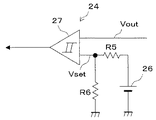
出力電圧検出回路24は、出力電圧モニタ端子Voとソフトスタート回路20との間に接続されており、出力電圧モニタ端子Voを介して与えられる出力電圧Voutが設定電圧より高いことを検出し、その検出信号をソフトスタート回路20に与える。このような出力電圧検出回路24は、例えば、図2に示す回路で構成することができる。
The output
図2は、図1に示す出力電圧検出回路24の電気的構成を示す回路図である。図2に示す出力電圧検出回路は、コンパレータ25、基準電源26、抵抗R5、R6から構成されており、コンパレータ25の一方の入力には基準電源26の電圧を抵抗R5、R6で分圧した設定電圧Vsetが与えられている。また、コンパレータ25の他方の入力には出力電圧モニタ端子Voを介して出力電圧Voutが与えられる。そして、コンパレータ25の出力はソフトスタート回路24に与えられる。
FIG. 2 is a circuit diagram showing an electrical configuration of the output
このような構成の出力電圧検出回路24は、出力電圧Voutと設定電圧Vsetとを比較してその比較結果信号をソフトスタート回路24に与える。例えば、この比較結果信号は出力電圧Voutが設定電圧Vsetよりも大きいときはHレベルになり、出力電圧Voutが設定電圧Vsetよりも小さいときはLレベルになる。そして、ソフトスタート回路20は、コントロール端子CTRLを介して与えられる輝度調整信号の立ち上がり時点での出力電圧検出回路24からの比較結果信号に応じてその動作/非動作を切り換えるようになっている。即ち、輝度調整信号が立ち上がった時点で比較結果信号がHレベルのときにはソフトスタート回路20は動作を停止し、Lレベルのときにはソフトスタート回路20は動作してドライブ回路13をソフトスタート制御する。以下に、図3を参照して図1に示す電源回路の動作を説明する。
The output
図3は、図10、図11と同様の図1に示す電源回路の各部の電圧波形及び電流波形を示す波形図である。図3において、(a)はコントロール端子CTRLに入力される輝度調整信号の電圧波形、(b)は出力電圧Voutの波形、(c)は入力電流Iinの波形を示している。尚、図3において、最初に輝度調整信号がHレベルに変化するときが図1に示す電源回路の起動時であり、このときに直流電源1から入力電圧Vinが供給される。そして、このときまで出力電圧Voutは0Vであり、出力コンデンサ5は全く充電されていない状態である。 FIG. 3 is a waveform diagram showing voltage waveforms and current waveforms of each part of the power supply circuit shown in FIG. 1 similar to FIGS. 3, (a) shows the voltage waveform of the luminance adjustment signal input to the control terminal CTRL, (b) shows the waveform of the output voltage Vout, and (c) shows the waveform of the input current Iin. In FIG. 3, the time when the luminance adjustment signal first changes to the H level is when the power supply circuit shown in FIG. Until this time, the output voltage Vout is 0 V, and the output capacitor 5 is not charged at all.
図3において、起動時、即ち、最初に輝度調整信号がHレベルになったとき(図3(a))、出力コンデンサ5は充電されていない状態であり、この時点での出力電圧Voutは設定電圧Vsetよりも小さい。従って、この時点での出力電圧検出回路24からの出力はLレベルであり、ソフトスタート回路20はこの時点での出力電圧検出回路24からの出力がLレベルであることを確認し動作を行う。従って、ドライブ回路13は昇圧動作を開始するが、ソフトスタート回路20がドライブ回路13を制御して出力デューティを徐々に変化させるので、出力電圧Voutは入力電圧Vinの電圧に成った後、電圧V1まで緩やかに上昇する(図3(b))。ここで、起動時の入力電流Iinは入力電圧Vinで出力コンデンサ5を充電する充電電流となるため、過大な電流とはならない(図3(c))。そして、出力コンデンサ5の充電が進むにつれて入力電流Iinは減少し、その後一定となる(図3(c))。
In FIG. 3, at the time of start-up, that is, when the luminance adjustment signal first becomes H level (FIG. 3A), the output capacitor 5 is not charged, and the output voltage Vout at this time is set. It is smaller than the voltage Vset. Therefore, the output from the output
次に、輝度調整信号がLレベルになると(図3(a))、ON/OFF回路21がドライブ回路13の昇圧動作を停止させるので、出力電圧Voutは直流電源1の入力電圧Vinとなり(図3(b))、入力電流Iinは流れなくなる(図3(c))。
Next, when the luminance adjustment signal becomes L level (FIG. 3A), the ON /
そして、その後、輝度調整のため輝度調整信号がHレベル/Lレベルに所定のデューティで切り換わるが(図3(a))、ソフトスタート回路20は輝度調整信号がHレベルになった時点での出力電圧検出回路24からの出力がHレベルであることを確認し動作を停止する。これは、このとき出力コンデンサ5は入力電圧Vinに充電されているため、出力電圧Voutは入力電圧Vinの電圧であり、この電圧は設定電圧Vsetよりも大きいからである。
After that, the luminance adjustment signal is switched to the H level / L level for a luminance adjustment with a predetermined duty (FIG. 3A), but the
従って、出力電圧Voutは輝度調整信号に応じて電圧V1とVinとに即座に切り換わる(図3(b))。ここで、出力電圧がVinからV1に切り換わるときに流れる入力電流Iinは、出力コンデンサ5が既に入力電圧Vinの電圧値に充電されているので、電圧V1から入力電圧Vinを差し引いた電圧で出力コンデンサ5を充電する充電電流となり、過大な電流とはならない(図3(c))。 Therefore, the output voltage Vout is immediately switched between the voltages V1 and Vin in accordance with the luminance adjustment signal (FIG. 3B). Here, the input current Iin that flows when the output voltage switches from Vin to V1 is output at a voltage obtained by subtracting the input voltage Vin from the voltage V1 because the output capacitor 5 has already been charged to the voltage value of the input voltage Vin. It becomes a charging current for charging the capacitor 5 and does not become an excessive current (FIG. 3C).
このようにして、起動時にはソフトスタート回路20により出力電圧Voutを緩やかに上昇させて入力電流Vinが過大にならないように制限するとともに、輝度調整信号に応じて昇圧動作の作動/停止を繰り返す場合は出力電圧Voutを所望の電圧に即座に立ち上げることができる。これにより、直流電源1にダメージを与えることなく、外部から与えられる輝度調整信号に応じた所望の輝度調整のできる電源回路が実現できる。
In this way, when starting up, the
図4は、図1に示す出力電圧検出回路24の他の電気的構成を示す回路図である。図4において、図2と同一の部分には同一の符号を付し、その説明を省略する。図4に示す出力電圧検出回路24が図2示す出力電圧検出回路24と相違する点は、コンパレータ25の代わりにヒステリシスを有するコンパレータ27が設けられている点である。コンパレータ27の一方の入力には基準電源26の電圧を抵抗R5、R6で分圧した設定電圧Vsetが与えられているが、この設定電圧Vsetはコンパレータ27の出力に応じたヒステリシスを有している。例えば、コンパレータ27の出力がLレベルのときの設定電圧Vsetは4.6Vになり、Hレベルのときの設定電圧Vsetは3.4Vになるようになっている。
FIG. 4 is a circuit diagram showing another electrical configuration of the output
このような図4に示す出力電圧検出回路24を用いた場合の図1に示す電源回路の動作を図3を参照して説明する。図3において、起動時、即ち、最初に輝度調整信号がHレベルになったとき(図3(a))、出力コンデンサ5は充電されていない状態であり、この時点での出力電圧Voutは4.6Vよりも小さいので、出力電圧検出回路24からの出力はLレベルである。
The operation of the power supply circuit shown in FIG. 1 when the output
そして、ソフトスタート回路20は出力電圧検出回路24からの出力がLレベルであるときにはソフトスタート動作を行い、出力電圧検出回路24からの出力がHレベルであるときには動作を停止するようになっている。従って、ドライブ回路13は昇圧動作を開始するが、ソフトスタート回路20がドライブ回路13の出力デューティを徐々に変化させるので、出力電圧Voutは入力電圧Vinの電圧に成った後、4.6Vになるまで、即ち、出力検出回路24内のコンパレータ27が反転するまで緩やかに上昇する(図3(b))。
The
そして、出力電圧Voutが4.6Vを超え出力検出回路24内のコンパレータ27が反転し出力がHレベルになると、ソフトスタート回路20は動作を停止するので、出力電圧Voutは電圧V1に即座に上昇する。しかしながら、このとき流れる入力電流Iinは出力コンデンサ5が既に4.6Vに充電されており、それを超える電圧上昇分での充電電流となるため、過大な電流とはならない。また、このとき、コンパレータ27の出力がHレベルになるので設定電圧Vsetは3.4Vに変化する。
When the output voltage Vout exceeds 4.6V and the
次に、輝度調整信号がLレベルになると(図3(a))、ON/OFF回路21がドライブ回路13の昇圧動作を停止させるので、出力電圧Voutは直流電源1の入力電圧Vinとなり(図3(b))、入力電流Iinは流れなくなる(図3(c))。
Next, when the luminance adjustment signal becomes L level (FIG. 3A), the ON /
そして、その後、輝度調整のため輝度調整信号はHレベル/Lレベルに所定のデューティで切り換わるが(図3(a))、ソフトスタート回路20は出力電圧検出回路24からの出力がHレベルであるので動作を停止している。これは、このとき出力コンデンサ5は入力電圧Vinに充電されているため、出力電圧Voutは入力電圧Vinの電圧であり、この電圧は3.4Vよりも大きいからである。
After that, the luminance adjustment signal is switched to H level / L level with a predetermined duty for luminance adjustment (FIG. 3A), but the
従って、出力電圧Voutは輝度調整信号に応じて電圧V1とVinとに即座に切り換わる(図3(b))。ここで、出力電圧がVinからV1に切り換わるときに流れる入力電流Iinは、出力コンデンサ5が既に入力電圧Vinの電圧値に充電されているので、電圧V1から入力電圧Vinを差し引いた電圧で出力コンデンサ5を充電する充電電流となり、過大な電流とはならない(図3(c))。 Therefore, the output voltage Vout is immediately switched between the voltages V1 and Vin in accordance with the luminance adjustment signal (FIG. 3B). Here, the input current Iin that flows when the output voltage switches from Vin to V1 is output at a voltage obtained by subtracting the input voltage Vin from the voltage V1 because the output capacitor 5 has already been charged to the voltage value of the input voltage Vin. It becomes a charging current for charging the capacitor 5 and does not become an excessive current (FIG. 3C).
このようにして、起動時にはソフトスタート回路20により出力電圧Voutを緩やかに上昇させて入力電流Vinが過大にならないように制限するとともに、輝度調整信号に応じて昇圧動作の作動/停止を繰り返す場合は出力電圧Voutを所望の電圧に即座に立ち上げることができる。この効果は図2に示す出力検出回路24を用いた場合でも同様であるが、図4に示す出力検出回路24を用いることで、スロースタート回路20は出力検出回路24からの出力に応じて動作/非動作を切り換えるだけで良く、スロースタート回路20を簡単な構成にすることができる。
In this way, when starting up, the
また、上述のように、設定電圧Vsetを4.6Vとすることで、直流電源1にリチウムイオン電池を使用した場合に、リチウムイオン電池の充電電圧の最大値までソフトスタート機能が働く状態を保つことができる。また、この設定電圧Vsetに1.2Vのヒステリシスを設け、出力電圧Voutが立ち上がった後に再びソフトスタート機能が働く電圧を3.4Vにすることにより、リチウムイオン電池の終止電圧の最下点までソフトスタート機能を無効にして使用することができ、電池を有効に使用することが可能となる。
Further, as described above, by setting the setting voltage Vset to 4.6 V, when a lithium ion battery is used for the
図5は、本発明の第2実施形態の電源回路の電気的構成を示す回路ブロック図である。図5において、図1と同一の部分には同一の符号を付し、その説明を省略する。図5に示す電源回路が図1に示す電源回路と相違する点は、出力電圧検出回路24の代わりにフィードバック検出回路28が設けられている点である。
FIG. 5 is a circuit block diagram showing an electrical configuration of the power supply circuit according to the second embodiment of the present invention. In FIG. 5, the same parts as those in FIG. The power supply circuit shown in FIG. 5 is different from the power supply circuit shown in FIG. 1 in that a
フィードバック検出回路28は、フィードバック端子FBとソフトスタート回路20との間に接続されており、フィードバック端子FBを介して与えられるフィードバック電圧Vfbが設定電圧より高いことを検出し、その検出信号をソフトスタート回路20に与える。図5に示す電源回路は、ソフトスタート回路20の動作/非動作の判断のために検出する電圧を出力電圧Voutからフィードバック電圧Vfbにしたものであり、フィードバック電圧Vfbは出力電圧Voutに比例した電圧であるので、フィードバック電圧検出回路30は、例えば、図2、図4に示す出力電圧検出回路24と同様の回路構成のものにし、設定電圧Vsetの電圧レベルを変更することで実現できる。従って、図5に示す電源回路は、図1に示す電源回路と同様の動作を行い、その効果も同様であるので、説明を省略する。
The
図6は、本発明の第3実施形態の電源回路の電気的構成を示す回路ブロック図である。図6において、図1と同一の部分には同一の符号を付し、その説明を省略する。図6に示す電源回路が図1に示す電源回路と相違する点は、過電圧保護回路23の代わりに出力電圧検出回路24の機能を兼用した過電圧保護回路29が設けられている点である。
FIG. 6 is a circuit block diagram showing an electrical configuration of the power supply circuit according to the third embodiment of the present invention. In FIG. 6, the same parts as those in FIG. The power supply circuit shown in FIG. 6 is different from the power supply circuit shown in FIG. 1 in that an
過電圧保護回路29は、図1に示す出力電圧検出回路24と過電圧保護回路23とを組み合わせたものである。図1に示す出力電圧検出回路24と過電圧保護回路23は、いずれも出力電圧Voutとそれぞれの回路に設定された所定の電圧とを比較してその比較結果の信号を出力する回路であるので、この2つの回路を組み合わせた過熱保護回路29にすることは容易に実現できる。例えば、図7に示すように、出力電圧Voutから抵抗分割で過電圧検出する電圧と出力電圧検出する電圧を取り出すようにすることで実現できる。このようにすると、電源回路の回路構成を簡素化することができる。
The
図8は、本発明の第4実施形態の電源回路の電気的構成を示す回路ブロック図である。図8において、図1と同一の部分には同一の符号を付し、その説明を省略する。図8に示す電源回路が図1に示す電源回路と相違する点は、出力電圧検出回路24の代わりに入力電圧検出回路30が設けられている点である。
FIG. 8 is a circuit block diagram showing an electrical configuration of the power supply circuit according to the fourth embodiment of the present invention. In FIG. 8, the same parts as those in FIG. The power supply circuit shown in FIG. 8 is different from the power supply circuit shown in FIG. 1 in that an input
入力電圧検出回路30は、電源端子Viとソフトスタート回路20との間に接続されており、電源端子Viを介して与えられる入力電圧Vinが設定電圧より高いことを検出し、その検出信号をソフトスタート回路20に与える。図7に示す電源回路は、ソフトスタート回路20の動作/非動作の判断のために検出する電圧を出力電圧Voutから入力電圧Vinにしたものであり、入力電圧検出回路30は、例えば、図2、図4に示す出力電圧検出回路24と同様の回路構成のものにし、設定電圧Vsetの電圧レベルを変更することで実現できる。
The input
起動時において、直流電源1からの入力電圧Vinが与えられると、入力コンデンサ2が充電され、それに伴い入力コンデンサ2の端子電圧は上昇する。従って、入力電圧Vinが完全に立ち上がるまでに入力電圧検出回路30で検出される入力電圧Vinは、設定電圧Vsetより低い状態であるので、入力電圧検出回路30はソフトスタート回路に検出信号を与え、ソフトスタート回路20がドライブ回路13をソフトスタート制御して出力電圧Voutを緩やかに上昇させることにより入力電流Iinを制限する。また、一旦起動した後は、入力電圧検出回路30で検出される入力電圧Vinは、設定電圧Vsetより高くなり、ソフトスタート回路20に検出信号を与えないのでソフトスタート回路20は動作を停止する。従って、出力電圧Voutは即座に立ち上がることになる。
When the input voltage Vin from the
これにより、図8に示す電源回路は、起動時にはソフトスタート回路20により出力電圧Voutを緩やかに上昇させて入力電流Vinが過大にならないように制限するとともに、輝度調整信号に応じて昇圧動作の作動/停止を繰り返す場合は出力電圧Voutを所望の電圧に即座に立ち上げることができる。
As a result, the power supply circuit shown in FIG. 8 restricts the output voltage Vout from being gently increased by the
また、図8に示す電源回路において、入力電圧検出回路30を図4に示すような設定電圧Vsetにヒステリシスを有する回路で構成し、設定電圧Vsetを4.2Vとすることで、直流電源1にリチウムイオン電池を使用した場合に、リチウムイオン電池の充電電圧の最大値までソフトスタート機能が働く状態を保つことができる。また、この設定電圧Vsetに1.2Vのヒステリシスを設け、出力電圧Voutが立ち上がった後に再びソフトスタート機能が働く電圧を3.0Vにすることにより、リチウムイオン電池の終止電圧の最下点までソフトスタート機能を無効にして使用することができ、電池を有効に使用することが可能となる。
Further, in the power supply circuit shown in FIG. 8, the input
また、以上説明した実施形態の電源回路を白色発光ダイオードLED1〜6を備えた携帯電話機等の電子機器に搭載すると、起動時にこの電子機器に内蔵されているリチウムイオン電池等の電池に流れる電流を制限して、この電池を終止電圧まで使用することができるとともに、白色発光ダイオードLED1〜6の輝度調整が可能な電子機器が実現できる。 Further, when the power supply circuit of the embodiment described above is mounted on an electronic device such as a mobile phone provided with the white light emitting diodes LED1 to 6, a current flowing in a battery such as a lithium ion battery built in the electronic device at the time of start-up is obtained. Limiting and using this battery up to the end voltage, an electronic device capable of adjusting the luminance of the white light emitting diodes LED1 to LED6 can be realized.
尚、本発明は上述の実施形態に限定されるものではなく、本発明の趣旨を逸脱しない範囲において各部の構成等を適宜に変更して実施することも可能である。 In addition, this invention is not limited to the above-mentioned embodiment, In the range which does not deviate from the meaning of this invention, it is also possible to change suitably the structure of each part, etc. and to implement.
以上説明したように、本発明によると、直流電源の一方の端子に接続されるコイルと、一端が前記コイルに接続され他端が前記直流電源の他方の端子に接続されるスイッチング素子と、該スイッチング素子と並列に接続される整流素子と出力コンデンサとの直列回路と、前記出力コンデンサと並列に接続される負荷と出力電流検出抵抗との直列回路と、前記負荷に流れる出力電流が一定になるように前記出力電流検出抵抗からのフィードバック電圧に基づいて前記スイッチング素子を駆動するドライブ回路とを備える電源回路において、前記整流素子と出力コンデンサとの接続点に発生する出力電圧を外部から調整するために、外部入力信号に応じて前記ドライブ回路の前記スイッチング素子の駆動動作を作動/停止する作動/停止回路と、前記出力電圧が所定の電圧より高いことを検出して検出信号を出力する出力電圧検出回路と、前記外部入力信号が入力されたときに前記出力電圧検出回路からの検出信号が与えられている場合は動作せず、与えられていない場合は前記出力電圧が緩やかに上昇するように前記ドライブ回路を制御するソフトスタート回路とを設けたので、起動時は、出力電圧が低いことを検出して前記ソフトスタート回路を動作させ、出力電圧を緩やかに上昇させることにより前記直流電源から流れる電流が過大になることを防ぎ、一旦、出力電圧が立ち上がった後は、外部入力信号に応じて前記ドライブ回路の前記スイッチング素子の駆動動作が作動/停止を繰り返す場合においても、前記ソフトスタート回路を動作させないようにすることで出力電圧を即座に立ち上げることができる。 As described above, according to the present invention, a coil connected to one terminal of a DC power supply, a switching element having one end connected to the coil and the other end connected to the other terminal of the DC power supply, A series circuit of a rectifying element and an output capacitor connected in parallel to the switching element, a series circuit of a load and an output current detection resistor connected in parallel to the output capacitor, and an output current flowing through the load are constant In a power supply circuit including a drive circuit that drives the switching element based on a feedback voltage from the output current detection resistor, the output voltage generated at the connection point between the rectifying element and the output capacitor is adjusted from the outside An operation / stop circuit for operating / stopping the driving operation of the switching element of the drive circuit according to an external input signal; An output voltage detection circuit that detects that the output voltage is higher than a predetermined voltage and outputs a detection signal, and a detection signal from the output voltage detection circuit when the external input signal is input Is not operated, and when not given, a soft start circuit is provided to control the drive circuit so that the output voltage rises slowly. By operating the soft start circuit and gradually increasing the output voltage, the current flowing from the DC power supply is prevented from becoming excessive. Once the output voltage rises, the drive circuit Even when the driving operation of the switching element is repeatedly activated / deactivated, the output voltage can be quickly adjusted by not operating the soft start circuit. It can be started up to.
また、このような電源回路を用いた電子機器にすることで、起動時には前記電子機器に内蔵されている直流電源からの電流を制限することができるとともに、起動後には前記電源回路から前記電子機器内の負荷に供給する電圧を前記電子機器からの信号によって調整可能な電子機器が実現でき、さらに、前記負荷が液晶表示装置のバックライトまたはフロントライトの発光素子であり、前記作動/停止回路が前記液晶表示装置のバックライトまたはフロントライトの輝度調整用回路であると、起動時に前記電子機器に内蔵されているリチウムイオン電池等の電池に流れる電流を制限して前記電池を終止電圧まで使用することができるとともに、前記電源回路で前記液晶表示装置のバックライトまたはフロントライトの輝度調整が可能な電子機器が実現できる。 Further, by making an electronic device using such a power supply circuit, it is possible to limit a current from a DC power source built in the electronic device at the time of startup, and from the power supply circuit to the electronic device after startup. An electronic device capable of adjusting a voltage supplied to an internal load by a signal from the electronic device can be realized. Further, the load is a light emitting element of a backlight or a front light of a liquid crystal display device, and the operation / stop circuit is In the backlight or front light brightness adjustment circuit of the liquid crystal display device, the current flowing to a battery such as a lithium ion battery built in the electronic device is limited at the time of start-up, and the battery is used up to the end voltage. An electronic device capable of adjusting the brightness of the backlight or the front light of the liquid crystal display device by the power supply circuit There can be realized.
1 直流電源
2 入力コンデンサ
3 コイル
4 ダイオード(整流素子)
5 出力コンデンサ
10 昇圧チョッパレギュレータ
11、12 FET(スイッチング素子)
13 ドライブ回路
14 電流検出コンパレータ
15 発振回路
16 アンプ
17 PWMコンパレータ
18 エラーコンパレータ
19、26 基準電源
20 ソフトスタート回路
21 ON/OFF回路(作動/停止回路)
22 過熱保護回路
23 過電圧保護回路
24 出力電圧検出回路
25、27 コンパレータ
28 フィードバック電圧検出回路
29 過電圧保護回路(出力電圧検出回路)
30 入力電圧検出回路
R1 抵抗(出力電流検出抵抗)
R2〜R6 抵抗
LED1〜LED6 白色発光ダイオード(負荷)
1
5
13
22
30 Input voltage detection circuit R1 resistance (output current detection resistance)
R2 to R6 Resistance LED1 to LED6 White light emitting diode (load)
Claims (7)
前記コイルの他端と負荷の一端との間に接続された整流素子と、
前記負荷に流れる出力電流を検出する出力電流検出抵抗と、
前記整流素子と前記負荷の接続点とグランド間に接続されて、充電されることによって出力電圧をその両端に発生する出力コンデンサと、
前記コイルの他端とグランド間に接続されたスイッチング素子と、
前記出力電流検出抵抗の両端に発生する電圧に応じて、前記スイッチング素子を第1のPWM方式で制御して前記出力電圧を昇圧させるドライブ回路と、
第2のPWM方式で制御された第1状態または第2状態をとる外部入力信号を受けるとともに、前記外部入力信号が第2状態の時には前記昇圧を停止させて、前記出力電流の量を制御する作動/停止回路と、
前記充電がなされていない状態で前記外部入力信号が第1状態となったときには、前記出力電圧を緩やかに立ち上げるように前記ドライブ回路を制御するソフトスタート処理を実行する一方、前記充電がなされている状態で前記外部入力信号が第1状態となったときには、前記ソフトスタート処理を実行しない、ソフトスタート回路と、
を設けたことを特徴とする電源回路。 A coil having one end connected to one of the DC power sources;
A rectifying element connected between the other end of the coil and one end of the load;
An output current detection resistor for detecting an output current flowing through the load;
An output capacitor that is connected between the connection point of the rectifying element and the load and the ground, and generates an output voltage at both ends by being charged;
A switching element connected between the other end of the coil and the ground;
A drive circuit that boosts the output voltage by controlling the switching element in a first PWM method according to a voltage generated across the output current detection resistor;
The external input signal that takes the first state or the second state controlled by the second PWM method is received, and when the external input signal is in the second state, the boosting is stopped and the amount of the output current is controlled. An activation / deactivation circuit;
When the external input signal becomes the first state when the charging is not performed, a soft start process is performed to control the drive circuit so that the output voltage is gradually raised, while the charging is performed. A soft start circuit that does not execute the soft start process when the external input signal is in a first state in a state in which
A power supply circuit comprising:
前記所定電圧は、
前記充電がなされているとともに前記昇圧が停止されている状態での前記出力電圧より小さく、かつ、前記充電がなされていないとともに前記昇圧が停止されている状態での前記出力電圧より大きく設定されていることを特徴とする請求項1に記載の電源回路。 An output voltage detection circuit that compares the output voltage with a predetermined voltage and outputs a comparison result signal that is a signal according to the comparison result to the soft start circuit;
The predetermined voltage is
The output voltage is smaller than the output voltage when the charge is performed and the boost is stopped, and is set larger than the output voltage when the charge is not performed and the boost is stopped. 2. The power supply circuit according to claim 1, wherein:
前記比較結果信号に基づいて、前記充電がなされているか否かを判別することを特徴とする請求項2に記載の電源回路。 The soft start circuit
The power supply circuit according to claim 2 , wherein it is determined whether or not the charging is performed based on the comparison result signal.
Priority Applications (3)
| Application Number | Priority Date | Filing Date | Title |
|---|---|---|---|
| JP2003393340A JP4052998B2 (en) | 2003-11-25 | 2003-11-25 | Power supply circuit and electronic device using the same |
| US10/982,826 US7129679B2 (en) | 2003-11-25 | 2004-11-08 | Power supply circuit having soft start |
| CNB2004100978241A CN100379135C (en) | 2003-11-25 | 2004-11-25 | Power supply circuit |
Applications Claiming Priority (1)
| Application Number | Priority Date | Filing Date | Title |
|---|---|---|---|
| JP2003393340A JP4052998B2 (en) | 2003-11-25 | 2003-11-25 | Power supply circuit and electronic device using the same |
Related Child Applications (1)
| Application Number | Title | Priority Date | Filing Date |
|---|---|---|---|
| JP2007126530A Division JP4558001B2 (en) | 2007-05-11 | 2007-05-11 | Power circuit |
Publications (3)
| Publication Number | Publication Date |
|---|---|
| JP2005160178A JP2005160178A (en) | 2005-06-16 |
| JP2005160178A5 JP2005160178A5 (en) | 2007-03-22 |
| JP4052998B2 true JP4052998B2 (en) | 2008-02-27 |
Family
ID=34587547
Family Applications (1)
| Application Number | Title | Priority Date | Filing Date |
|---|---|---|---|
| JP2003393340A Expired - Fee Related JP4052998B2 (en) | 2003-11-25 | 2003-11-25 | Power supply circuit and electronic device using the same |
Country Status (3)
| Country | Link |
|---|---|
| US (1) | US7129679B2 (en) |
| JP (1) | JP4052998B2 (en) |
| CN (1) | CN100379135C (en) |
Families Citing this family (97)
| Publication number | Priority date | Publication date | Assignee | Title |
|---|---|---|---|---|
| JP4743570B2 (en) * | 2001-04-10 | 2011-08-10 | ルネサスエレクトロニクス株式会社 | Semiconductor integrated circuit with built-in power supply circuit, liquid crystal display control device, and portable electronic device |
| US10734896B2 (en) | 2003-07-07 | 2020-08-04 | Rohm Co., Ltd. | Load driving device, and lighting apparatus and liquid crystal display device using the same |
| US8519680B2 (en) | 2003-07-07 | 2013-08-27 | Rohm Co., Ltd. | Load driving device, and lighting apparatus and liquid crystal display device using the same |
| JP4785410B2 (en) * | 2004-06-01 | 2011-10-05 | セイコーインスツル株式会社 | Electronic device having a booster circuit |
| US8552963B2 (en) * | 2004-11-30 | 2013-10-08 | Rohm Co., Ltd. | Switching regulator control circuit, current drive circuit, light emitting apparatus, and information terminal apparatus |
| WO2006064841A1 (en) * | 2004-12-14 | 2006-06-22 | Matsushita Electric Industrial Co., Ltd. | Semiconductor circuit for driving light emitting diode, and light emitting diode driving apparatus |
| EP1691581B1 (en) * | 2005-02-11 | 2015-10-07 | STMicroelectronics Srl | Power-efficient led drive circuit |
| US7317302B1 (en) * | 2005-03-04 | 2008-01-08 | National Semiconductor Corporation | Converter with feedback voltage referenced to output voltage |
| US7375476B2 (en) * | 2005-04-08 | 2008-05-20 | S.C. Johnson & Son, Inc. | Lighting device having a circuit including a plurality of light emitting diodes, and methods of controlling and calibrating lighting devices |
| JP2006324534A (en) * | 2005-05-20 | 2006-11-30 | Seiko Instruments Inc | Light emitting diode driving circuit |
| JP5175427B2 (en) * | 2005-05-31 | 2013-04-03 | Necディスプレイソリューションズ株式会社 | Light emitting element driving device |
| KR100810516B1 (en) * | 2005-07-01 | 2008-03-10 | 삼성전자주식회사 | Load driving apparatus and load driving method thereof |
| JP4773165B2 (en) * | 2005-08-31 | 2011-09-14 | 株式会社ダイヘン | High frequency power supply |
| KR100727354B1 (en) * | 2005-11-09 | 2007-06-13 | 주식회사 유양정보통신 | Constant Current Pulse Width Modulation Driving Circuit for Light Emitting Diode |
| CN1980507B (en) * | 2005-12-07 | 2010-05-26 | 群康科技(深圳)有限公司 | Starting circuit and back-light starting circuit |
| US7208927B1 (en) * | 2005-12-09 | 2007-04-24 | Monolithic Power Systems, Inc. | Soft start system and method for switching regulator |
| EP1982560A1 (en) * | 2006-01-31 | 2008-10-22 | Koninklijke Philips Electronics N.V. | Led driver circuit |
| KR100917623B1 (en) | 2006-02-13 | 2009-09-17 | 삼성전자주식회사 | LED Driving Apparatus |
| JP2007281424A (en) | 2006-03-15 | 2007-10-25 | Casio Comput Co Ltd | Driving device for light emitting element, method of driving light emitting element, and driving program for light emitting element |
| US7649325B2 (en) * | 2006-04-03 | 2010-01-19 | Allegro Microsystems, Inc. | Methods and apparatus for switching regulator control |
| DE102006030655A1 (en) * | 2006-04-21 | 2007-10-25 | Tridonicatco Gmbh & Co. Kg | Emergency lighting device for operating a light source, in particular an LED |
| JP4895694B2 (en) * | 2006-06-08 | 2012-03-14 | ルネサスエレクトロニクス株式会社 | Power circuit |
| US7705547B2 (en) * | 2006-10-19 | 2010-04-27 | Honeywell International Inc. | High-side current sense hysteretic LED controller |
| CN1968553B (en) * | 2006-11-27 | 2010-05-12 | 鹤山丽得电子实业有限公司 | Soft-start type LED lamp string controller |
| US7675245B2 (en) * | 2007-01-04 | 2010-03-09 | Allegro Microsystems, Inc. | Electronic circuit for driving a diode load |
| CN101231815B (en) * | 2007-01-23 | 2010-09-22 | 立锜科技股份有限公司 | Energy saving control circuit of organic luminous panel and method thereof |
| KR20100014890A (en) | 2007-02-13 | 2010-02-11 | 오스람 게젤샤프트 미트 베쉬랭크터 하프퉁 | Led module and method for operating at least one led |
| JP5352964B2 (en) * | 2007-03-29 | 2013-11-27 | 富士通セミコンダクター株式会社 | DC-DC converter, power supply voltage supply method, power supply voltage supply system, and control method for DC-DC converter |
| KR100867551B1 (en) * | 2007-05-18 | 2008-11-10 | 삼성전기주식회사 | Led array driving apparatus |
| GB2451467B (en) * | 2007-07-28 | 2013-01-16 | Zetex Semiconductors Plc | Current driving method and circuit |
| US10938303B2 (en) | 2007-08-10 | 2021-03-02 | Rohm Co., Ltd. | Driving device |
| JP2009044081A (en) * | 2007-08-10 | 2009-02-26 | Rohm Co Ltd | Driver |
| KR101614304B1 (en) | 2007-11-16 | 2016-04-21 | 알레그로 마이크로시스템스, 엘엘씨 | Electronic circuits for driving series connected light emitting diode strings |
| CN101471577B (en) | 2007-12-29 | 2011-06-15 | 比亚迪股份有限公司 | Voltage balance circuit for double-burl chargeable battery |
| CN101471602B (en) | 2007-12-29 | 2012-11-07 | 比亚迪股份有限公司 | Bidirectional DC power supply circuit |
| US8665188B2 (en) * | 2008-02-04 | 2014-03-04 | National Semiconductor Corporation | Laser diode / LED drive circuit |
| JP5071134B2 (en) * | 2008-02-05 | 2012-11-14 | ミツミ電機株式会社 | DC power supply, LED drive power supply, and power supply semiconductor integrated circuit |
| CN101541117B (en) * | 2008-03-21 | 2013-07-03 | 鹏智科技(深圳)有限公司 | Electronic device with function of LED illumination control and control method thereof |
| US8432108B2 (en) * | 2008-04-30 | 2013-04-30 | Lsi Industries, Inc. | Solid state lighting, driver circuits, and related software |
| US7999487B2 (en) * | 2008-06-10 | 2011-08-16 | Allegro Microsystems, Inc. | Electronic circuit for driving a diode load with a predetermined average current |
| US7868595B1 (en) | 2008-06-17 | 2011-01-11 | National Semiconductor Corporation | Apparatus and method for soft-start mode transition in a switching regulator |
| JP5334507B2 (en) * | 2008-09-10 | 2013-11-06 | セミコンダクター・コンポーネンツ・インダストリーズ・リミテッド・ライアビリティ・カンパニー | Light emitting element driving circuit and mobile phone |
| TWI380548B (en) * | 2008-12-16 | 2012-12-21 | Delta Electronics Inc | Error detecting and motor protecting apparatus and method thereof |
| JP2010178438A (en) * | 2009-01-27 | 2010-08-12 | Sanyo Electric Co Ltd | Switching power control circuit |
| JP5365686B2 (en) * | 2009-03-13 | 2013-12-11 | 富士電機株式会社 | Switching power supply device, integrated circuit, and operation state setting method of switching power supply device |
| JP2010263711A (en) * | 2009-05-08 | 2010-11-18 | Renesas Electronics Corp | Input overvoltage protection circuit with soft start function |
| CN101894530B (en) * | 2009-05-19 | 2015-05-06 | 罗姆股份有限公司 | Driving circuit and protection method thereof, light-emitting device and display device |
| US8427069B2 (en) * | 2009-06-22 | 2013-04-23 | Polar Semiconductor, Inc. | Current-regulated power supply with soft-start protection |
| TWI420964B (en) * | 2009-08-24 | 2013-12-21 | Green Solution Tech Co Ltd | Driving circuit and controller for controlling the same |
| CN102033565B (en) * | 2009-09-24 | 2013-03-13 | 上海华虹Nec电子有限公司 | Voltage reference circuit |
| US8232791B2 (en) * | 2009-10-05 | 2012-07-31 | World Properties, Inc. | Soft starting driver for piezoelectric device |
| JP5618733B2 (en) * | 2009-12-09 | 2014-11-05 | ローム株式会社 | Semiconductor device and switching regulator using the same |
| US8327165B2 (en) * | 2010-01-21 | 2012-12-04 | Dell Products L.P. | Soft start with active reset |
| US9147911B2 (en) * | 2010-04-08 | 2015-09-29 | Bae Systems Information And Electronic Systems Integration Inc. | Method of extending the shelf-life of a coin cell in an application requiring high pulse current |
| KR101129287B1 (en) | 2010-05-11 | 2012-03-27 | 주식회사 디엠비테크놀로지 | LED Driving System |
| KR101107360B1 (en) | 2010-05-14 | 2012-01-19 | 엘지이노텍 주식회사 | Apparatus for supplying power of light emitting diode backlight |
| CN102014541B (en) * | 2010-05-18 | 2011-12-14 | 凹凸电子(武汉)有限公司 | Light source driving circuit and method for regulating electric power of light source |
| EP2398298A3 (en) * | 2010-05-24 | 2012-03-14 | ADB Airfield Solutions LLC | Power supply for an airfield LED sign |
| TWI403875B (en) * | 2010-06-17 | 2013-08-01 | O2Micro Int Ltd | Light source driving circuit and method for adjusting power of light source |
| DE102010048755A1 (en) * | 2010-10-16 | 2012-04-19 | Hella Kgaa Hueck & Co. | Circuit arrangement for supplying power to LEDs, has selection element for selecting capacitor, and resistors for adjusting potential at input for soft start of direct current to direct current converter |
| JP2012090387A (en) * | 2010-10-18 | 2012-05-10 | Panasonic Corp | Dc-dc converter |
| IT1403159B1 (en) | 2010-12-02 | 2013-10-04 | Osram Spa | CONVERTER DEVICE. |
| US8476842B2 (en) * | 2010-12-08 | 2013-07-02 | Excelliance Mos Corporation | Driving device for LED module |
| US8692482B2 (en) | 2010-12-13 | 2014-04-08 | Allegro Microsystems, Llc | Circuitry to control a switching regulator |
| KR101069556B1 (en) | 2010-12-28 | 2011-10-05 | 주식회사 케이지테크 | Illumination power led driving circuit |
| JP5569406B2 (en) * | 2011-01-18 | 2014-08-13 | 株式会社富士通ゼネラル | Air conditioner |
| US9101025B2 (en) * | 2011-01-31 | 2015-08-04 | Marvell World Trade Ltd. | Systems and methods for driving light emitting diodes |
| JP5587283B2 (en) * | 2011-02-02 | 2014-09-10 | 旭化成エレクトロニクス株式会社 | Power supply circuit and control method of power supply circuit |
| JP5740471B2 (en) * | 2011-05-27 | 2015-06-24 | ローム株式会社 | LOAD DRIVE DEVICE AND ELECTRONIC DEVICE USING THE SAME |
| US9155156B2 (en) | 2011-07-06 | 2015-10-06 | Allegro Microsystems, Llc | Electronic circuits and techniques for improving a short duty cycle behavior of a DC-DC converter driving a load |
| US9265104B2 (en) | 2011-07-06 | 2016-02-16 | Allegro Microsystems, Llc | Electronic circuits and techniques for maintaining a consistent power delivered to a load |
| TW201318476A (en) * | 2011-10-21 | 2013-05-01 | Luxul Technology Inc | AC LED device with continuous dimming |
| US9225243B2 (en) | 2011-12-28 | 2015-12-29 | Osram Gmbh | Converter device |
| US9426862B2 (en) * | 2012-04-12 | 2016-08-23 | Shenzhen China Star Optoelectronics Technology Co., Ltd. | LED backlight drive circuit, liquid crystal display device and driving method |
| US8957607B2 (en) | 2012-08-22 | 2015-02-17 | Allergo Microsystems, LLC | DC-DC converter using hysteretic control and associated methods |
| US9144126B2 (en) | 2012-08-22 | 2015-09-22 | Allegro Microsystems, Llc | LED driver having priority queue to track dominant LED channel |
| JP6036024B2 (en) * | 2012-08-31 | 2016-11-30 | 東芝ライテック株式会社 | Lighting device |
| CN102970500B (en) * | 2012-11-16 | 2015-06-03 | 深圳创维-Rgb电子有限公司 | Liquid crystal display television and power supply circuit thereof |
| JP6034161B2 (en) * | 2012-11-29 | 2016-11-30 | シナプティクス・ジャパン合同会社 | Semiconductor device and electronic equipment |
| US8982521B2 (en) * | 2013-01-21 | 2015-03-17 | Shenzhen China Star | Overvoltage protection method for backlight driver |
| US8994279B2 (en) | 2013-01-29 | 2015-03-31 | Allegro Microsystems, Llc | Method and apparatus to control a DC-DC converter |
| US9285812B2 (en) * | 2013-02-01 | 2016-03-15 | Allegro Microsystems, Llc | Soft start circuits and techniques |
| CN103368390A (en) * | 2013-07-15 | 2013-10-23 | 长城电器集团有限公司 | Power supply system of automatic reclosing lock breaker in time of electric leakage |
| CN103595018B (en) * | 2013-11-07 | 2017-02-08 | 深圳市华星光电技术有限公司 | Over-voltage protecting circuit, LED backlight drive circuit and liquid crystal displayer |
| JP6273642B2 (en) * | 2013-12-16 | 2018-02-07 | パナソニックIpマネジメント株式会社 | LED lighting device |
| CN104795848A (en) * | 2014-01-16 | 2015-07-22 | 纬创资通股份有限公司 | Power management method and display device |
| CN103746571B (en) * | 2014-01-21 | 2016-06-08 | 上海镭芯微电子有限公司 | A kind of supply unit adapting to pulse output loading |
| CN106716804B (en) * | 2014-06-30 | 2019-08-30 | 天工方案公司 | Circuit, device and method for the voltage adjusting in bypass voltage adjuster |
| CN104917366A (en) * | 2015-06-23 | 2015-09-16 | 杭州中恒派威电源有限公司 | Quasi-resonant Boost soft start circuit |
| KR20170002324A (en) * | 2015-06-29 | 2017-01-06 | 페어차일드코리아반도체 주식회사 | Switch control circuit and converter comprising the same |
| FR3046329B1 (en) * | 2015-12-24 | 2019-12-13 | STMicroelectronics (Alps) SAS | DEVICE FOR CONTROLLING A DIODE |
| US9954432B2 (en) * | 2016-07-04 | 2018-04-24 | Han-Win Technology Co. Ltd. | Power supply apparatus with soft-start and protection |
| KR101815859B1 (en) * | 2017-01-04 | 2018-01-08 | 한국과학기술원 | Power management device |
| US10615669B2 (en) * | 2018-01-12 | 2020-04-07 | Littelfuse, Inc. | Protection device and system using negative capacitance component |
| CN108923388A (en) * | 2018-08-17 | 2018-11-30 | 东菱技术有限公司 | A kind of fault detection circuit powering on buffer cell and method |
| US10447145B1 (en) | 2018-11-19 | 2019-10-15 | Stmicroelectronics (Grenoble 2) Sas | SMPS power-on with energy saver |
| CN110351922B (en) * | 2019-05-30 | 2021-06-11 | 鹰潭阳光照明有限公司 | Intelligent dimmable LED lamp |
Family Cites Families (11)
| Publication number | Priority date | Publication date | Assignee | Title |
|---|---|---|---|---|
| US5350997A (en) * | 1992-12-16 | 1994-09-27 | International Business Machines Corporation | Step-up voltage converter with overcurrent protection |
| JP3204172B2 (en) | 1997-08-06 | 2001-09-04 | 株式会社豊田自動織機製作所 | Switching power supply |
| US5998977A (en) * | 1998-05-27 | 1999-12-07 | Maxim Integrated Products, Inc. | Switching power supplies with linear precharge, pseudo-buck and pseudo-boost modes |
| JP3236573B2 (en) * | 1999-02-25 | 2001-12-10 | 長野日本無線株式会社 | Switching power supply |
| US6198258B1 (en) * | 1999-04-28 | 2001-03-06 | Rohm Co., Ltd. | DC-DC converter capable of soft starting function by slowly raising reference voltage |
| JP2000324807A (en) | 1999-05-10 | 2000-11-24 | Seiko Instruments Inc | Switching regulator |
| US6185082B1 (en) * | 1999-06-01 | 2001-02-06 | System General Corporation | Protection circuit for a boost power converter |
| CN1074602C (en) * | 1999-12-18 | 2001-11-07 | 深圳市安圣电气有限公司 | Thick film circuit for driver control of switching voltage regulator |
| AU2001265965A1 (en) * | 2000-05-19 | 2001-12-03 | Telefonaktiebolaget Lm Ericsson (Publ) | Dc/dc converters |
| US6737845B2 (en) * | 2001-06-21 | 2004-05-18 | Champion Microelectronic Corp. | Current inrush limiting and bleed resistor current inhibiting in a switching power converter |
| JP4094487B2 (en) * | 2003-05-21 | 2008-06-04 | ローム株式会社 | Power supply for positive / negative output voltage |
-
2003
- 2003-11-25 JP JP2003393340A patent/JP4052998B2/en not_active Expired - Fee Related
-
2004
- 2004-11-08 US US10/982,826 patent/US7129679B2/en not_active Expired - Fee Related
- 2004-11-25 CN CNB2004100978241A patent/CN100379135C/en not_active Expired - Fee Related
Also Published As
| Publication number | Publication date |
|---|---|
| US20050110469A1 (en) | 2005-05-26 |
| CN1622438A (en) | 2005-06-01 |
| JP2005160178A (en) | 2005-06-16 |
| US7129679B2 (en) | 2006-10-31 |
| CN100379135C (en) | 2008-04-02 |
Similar Documents
| Publication | Publication Date | Title |
|---|---|---|
| JP4052998B2 (en) | Power supply circuit and electronic device using the same | |
| JP4728718B2 (en) | STEP-UP SWITCHING REGULATOR, ITS CONTROL CIRCUIT, AND ELECTRONIC DEVICE USING THE SAME | |
| US9674909B2 (en) | Driving circuit for light-emitting element with burst dimming control | |
| JP5174390B2 (en) | Power supply device and electronic apparatus equipped with the same | |
| JP4510022B2 (en) | Power supply device and electronic device using the same | |
| JP4429868B2 (en) | Switching power supply circuit and electronic device using the same | |
| JP4127559B2 (en) | POWER CIRCUIT DEVICE AND ELECTRONIC DEVICE HAVING THE POWER CIRCUIT DEVICE | |
| US20070200540A1 (en) | Power Source Device | |
| JP2009033867A (en) | Charge pump circuit, its control circuit, and its control method | |
| JP2008177019A (en) | Led drive circuit | |
| JP4236602B2 (en) | Switching power supply circuit and electronic device using the same | |
| US8076917B2 (en) | Buck switching regulator with improved mode transition and control method thereof | |
| JP2008060492A (en) | Light-emitting device drive | |
| JP4558001B2 (en) | Power circuit | |
| JP5214219B2 (en) | Charge pump circuit and control circuit thereof | |
| KR100641259B1 (en) | Boost switching regulator circuit | |
| JP4328710B2 (en) | Boost DC / DC converter | |
| JP5290565B2 (en) | Charge pump circuit and control circuit thereof | |
| JP2009118589A (en) | Dc voltage booster circuit and guiding light device | |
| JP2006174630A (en) | Method and circuit for controlling switching regulator and power supply unit | |
| JP4778870B2 (en) | Power supply device having negative power supply circuit | |
| KR20050092493A (en) | Device for protect circuiting of lcd backlight | |
| JP2018060593A (en) | Driving circuit | |
| CN115802544A (en) | Light emitting diode dimming driving circuit working at low power supply voltage | |
| JP5947082B2 (en) | Circuit and method for driving a light source |
Legal Events
| Date | Code | Title | Description |
|---|---|---|---|
| A621 | Written request for application examination |
Free format text: JAPANESE INTERMEDIATE CODE: A621 Effective date: 20060125 |
|
| A521 | Written amendment |
Free format text: JAPANESE INTERMEDIATE CODE: A523 Effective date: 20070206 |
|
| A871 | Explanation of circumstances concerning accelerated examination |
Free format text: JAPANESE INTERMEDIATE CODE: A871 Effective date: 20070206 |
|
| A975 | Report on accelerated examination |
Free format text: JAPANESE INTERMEDIATE CODE: A971005 Effective date: 20070314 |
|
| A131 | Notification of reasons for refusal |
Free format text: JAPANESE INTERMEDIATE CODE: A131 Effective date: 20070320 |
|
| A521 | Written amendment |
Free format text: JAPANESE INTERMEDIATE CODE: A523 Effective date: 20070514 |
|
| A131 | Notification of reasons for refusal |
Free format text: JAPANESE INTERMEDIATE CODE: A131 Effective date: 20070828 |
|
| RD01 | Notification of change of attorney |
Free format text: JAPANESE INTERMEDIATE CODE: A7421 Effective date: 20070910 |
|
| A521 | Written amendment |
Free format text: JAPANESE INTERMEDIATE CODE: A523 Effective date: 20071019 |
|
| TRDD | Decision of grant or rejection written | ||
| A01 | Written decision to grant a patent or to grant a registration (utility model) |
Free format text: JAPANESE INTERMEDIATE CODE: A01 Effective date: 20071204 |
|
| A61 | First payment of annual fees (during grant procedure) |
Free format text: JAPANESE INTERMEDIATE CODE: A61 Effective date: 20071204 |
|
| FPAY | Renewal fee payment (event date is renewal date of database) |
Free format text: PAYMENT UNTIL: 20101214 Year of fee payment: 3 |
|
| R150 | Certificate of patent or registration of utility model |
Free format text: JAPANESE INTERMEDIATE CODE: R150 |
|
| FPAY | Renewal fee payment (event date is renewal date of database) |
Free format text: PAYMENT UNTIL: 20101214 Year of fee payment: 3 |
|
| FPAY | Renewal fee payment (event date is renewal date of database) |
Free format text: PAYMENT UNTIL: 20111214 Year of fee payment: 4 |
|
| FPAY | Renewal fee payment (event date is renewal date of database) |
Free format text: PAYMENT UNTIL: 20111214 Year of fee payment: 4 |
|
| FPAY | Renewal fee payment (event date is renewal date of database) |
Free format text: PAYMENT UNTIL: 20121214 Year of fee payment: 5 |
|
| LAPS | Cancellation because of no payment of annual fees |