WO2012165149A1 - アンテナ装置および通信端末装置 - Google Patents
アンテナ装置および通信端末装置 Download PDFInfo
- Publication number
- WO2012165149A1 WO2012165149A1 PCT/JP2012/062577 JP2012062577W WO2012165149A1 WO 2012165149 A1 WO2012165149 A1 WO 2012165149A1 JP 2012062577 W JP2012062577 W JP 2012062577W WO 2012165149 A1 WO2012165149 A1 WO 2012165149A1
- Authority
- WO
- WIPO (PCT)
- Prior art keywords
- conductor
- coil
- coiled conductor
- magnetic flux
- coiled
- Prior art date
- Legal status (The legal status is an assumption and is not a legal conclusion. Google has not performed a legal analysis and makes no representation as to the accuracy of the status listed.)
- Ceased
Links
Images





Classifications
-
- H—ELECTRICITY
- H01—ELECTRIC ELEMENTS
- H01Q—ANTENNAS, i.e. RADIO AERIALS
- H01Q1/00—Details of, or arrangements associated with, antennas
- H01Q1/50—Structural association of antennas with earthing switches, lead-in devices or lightning protectors
-
- H—ELECTRICITY
- H03—ELECTRONIC CIRCUITRY
- H03H—IMPEDANCE NETWORKS, e.g. RESONANT CIRCUITS; RESONATORS
- H03H7/00—Multiple-port networks comprising only passive electrical elements as network components
- H03H7/38—Impedance-matching networks
-
- H—ELECTRICITY
- H04—ELECTRIC COMMUNICATION TECHNIQUE
- H04B—TRANSMISSION
- H04B1/00—Details of transmission systems, not covered by a single one of groups H04B3/00 - H04B13/00; Details of transmission systems not characterised by the medium used for transmission
- H04B1/02—Transmitters
- H04B1/04—Circuits
- H04B1/0458—Arrangements for matching and coupling between power amplifier and antenna or between amplifying stages
-
- H—ELECTRICITY
- H01—ELECTRIC ELEMENTS
- H01F—MAGNETS; INDUCTANCES; TRANSFORMERS; SELECTION OF MATERIALS FOR THEIR MAGNETIC PROPERTIES
- H01F19/00—Fixed transformers or mutual inductances of the signal type
- H01F19/04—Transformers or mutual inductances suitable for handling frequencies considerably beyond the audio range
Definitions
- communication terminals including mobile phones have been used in communication systems such as GSM (registered trademark) (Global System for mobile Communications), DCS (Digital Communication System), PCS (Personal Communication Service), UMTS (Universal Mobile Telecommunications System), Furthermore, it may be required to support GPS (Global Positioning System), wireless LAN, Bluetooth (registered trademark), and the like. Therefore, the antenna device in such a communication terminal device is required to cover a wide frequency band from 800 MHz to 2.4 GHz.
- GSM Global System for mobile Communications
- DCS Digital Communication System
- PCS Personal Communication Service
- UMTS Universal Mobile Telecommunications System
- GPS Global Positioning System
- wireless LAN wireless local area network
- Bluetooth registered trademark
- an antenna device having a broadband matching circuit constituted by an LC parallel resonance circuit or an LC series resonance circuit is generally used. Is. Further, as an antenna device corresponding to a wide frequency band, for example, tunable antennas as disclosed in Patent Document 3 and Patent Document 4 are known.
- JP 2004-336250 A JP 2006-173697 A JP 2000-124728 A JP 2008-035065 A
- the matching circuits shown in Patent Documents 1 and 2 include a plurality of resonant circuits, the insertion loss in the matching circuit tends to increase and a sufficient gain may not be obtained.
- the tunable antennas disclosed in Patent Documents 3 and 4 require a circuit for controlling the variable capacitance element, that is, a switching circuit for switching the frequency band, so that the circuit configuration tends to be complicated. In addition, since a loss and distortion in the switching circuit are large, a sufficient gain may not be obtained.
- the present invention has been made in view of the above-described circumstances, and an object of the present invention is to provide an antenna device that impedance matches with a power feeding circuit in a wide frequency band, and a communication terminal device including the antenna device.
- An antenna device of the present invention is an antenna device including an antenna element and an impedance conversion circuit connected to the antenna element,
- the impedance conversion circuit includes a transformer-type circuit in which a first inductance element and a second inductance element are coupled through mutual inductance, The first end of the first inductance element is connected to the feeder circuit, and the second end is connected to the ground, A first end of the second inductance element is connected to the feeder circuit, and a second end is connected to the antenna element;
- the mutual inductance is larger than the inductance of the second inductance element.
- the first inductance element includes a first coil-shaped conductor and a second coil-shaped conductor
- the second inductance element includes a third coil-shaped conductor and a fourth coil-shaped conductor
- the first coil-shaped conductor and the second coil-shaped conductor are wound so that a closed loop of a first magnetic flux is generated by the first coil-shaped conductor and the second coil-shaped conductor so as to be electromagnetically coupled.
- the third coil-shaped conductor and the fourth coil-shaped conductor are wound so that a closed loop of the second magnetic flux is generated by the third coil-shaped conductor and the fourth coil-shaped conductor to be electromagnetically coupled. It is preferable that it is turned.
- the first coiled conductor, the second coiled conductor, the third coiled conductor, and the fourth coiled conductor have a closed loop of the first magnetic flux. It is preferable that the rotating magnetic flux (magnetic flux passing through the first closed magnetic path) and the magnetic flux rotating around the closed loop of the second magnetic flux (magnetic flux passing through the second closed magnetic path) are wound in opposite directions. .
- the first coiled conductor and the third coiled conductor are coupled to each other via a magnetic field and an electric field
- the second coiled conductor and the fourth coiled conductor are coupled to each other via a magnetic field and an electric field;
- the first coiled conductor, the second coiled conductor, the third coiled conductor, and the fourth coiled conductor are It is preferable that the conductive pattern is formed of a laminated body in which a plurality of dielectric layers or magnetic layers are laminated.
- the winding axis of each of the first coiled conductor, the second coiled conductor, the third coiled conductor, and the fourth coiled conductor is the laminated body. Facing in the stacking direction, The first coiled conductor and the second coiled conductor are juxtaposed with each other with different winding axes, The third coiled conductor and the fourth coiled conductor are juxtaposed with each other with different winding axes, Each winding range of the first coiled conductor and the third coiled conductor overlaps at least partially in plan view, and each winding range of the second coiled conductor and the fourth coiled conductor Are preferably overlapped at least partially in plan view.
- the impedance conversion circuit further includes a fifth coil-shaped conductor and a sixth coil-shaped conductor, The fifth coil-shaped conductor and the sixth coil-shaped conductor are connected in series to form a third inductance element, The fifth coil-shaped conductor and the sixth coil-shaped conductor are electromagnetically coupled by the fifth coil-shaped conductor and the sixth coil-shaped conductor generating a closed loop of the third magnetic flux (the third closed magnetic circuit is Configured), and A first end of the third inductance element is connected to the feeder circuit; a second end of the third inductance element is connected to the ground; The first coiled conductor, the second coiled conductor, the third coiled conductor, the fourth coiled conductor, the fifth coiled conductor and the sixth coiled conductor are It is preferable that the magnetic fluxes traveling around the closed loop of the second magnetic flux are sandwiched between the magnetic fluxes traveling around the closed loop of the first magnetic flux and the magnetic fluxes traveling around the closed
- the impedance conversion circuit further includes a fifth coil-shaped conductor and a sixth coil-shaped conductor, The fifth coil-shaped conductor and the sixth coil-shaped conductor are connected in series to form a third inductance element, The fifth coil-shaped conductor and the sixth coil-shaped conductor are electromagnetically coupled by the fifth coil-shaped conductor and the sixth coil-shaped conductor generating a closed loop of the third magnetic flux (the third closed magnetic circuit is Configured), and A first end of the third inductance element is connected to the feeder circuit; a second end of the third inductance element is connected to the ground; The first coiled conductor, the second coiled conductor, the third coiled conductor, the fourth coiled conductor, and the fifth coiled conductor go around a closed loop of the first magnetic flux. It is preferable that the magnetic flux is arranged so as to be sandwiched in the layer direction by the magnetic flux that goes around the closed loop of the second magnetic flux and the magnetic flux that goes around the closed
- a communication terminal device includes an antenna device including an antenna element, a power feeding circuit, and an impedance conversion circuit connected between the antenna element and the power feeding circuit.
- the impedance conversion circuit includes at least a first coiled conductor, a second coiled conductor, a third coiled conductor, and a fourth coiled conductor,
- the impedance conversion circuit includes a transformer-type circuit in which a first inductance element and a second inductance element are coupled through mutual inductance, The first end of the first inductance element is connected to the feeder circuit, and the second end is connected to the ground, A first end of the second inductance element is connected to the feeder circuit, and a second end is connected to the antenna element;
- the mutual inductance is larger than the inductance of the second inductance element.
- an insertion loss in a matching circuit is small, a switching circuit for switching a frequency band is unnecessary, and an antenna device that impedance-matches with a power feeding circuit over a wide frequency band, and a communication terminal device including the antenna device. Can be configured.
- the communication terminal apparatus of the present invention since the antenna apparatus is used, it is possible to realize a communication terminal apparatus that can support various communication systems having different frequency bands.
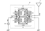
- FIG. 1A is a circuit diagram of the main part of the impedance conversion circuit 35 included in the antenna device 101 of the first embodiment
- FIG. 1B is a circuit diagram of the antenna device 101
- FIG. 2 is a diagram in which various arrows indicating states of magnetic field coupling and electric field coupling are written in the circuit illustrated in FIG.
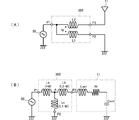
- FIG. 3A is a circuit diagram obtained by equivalently converting the antenna device 101 of the first embodiment
- FIG. 3B is a circuit diagram obtained by further equivalently converting it.
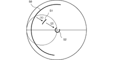
- FIG. 4 is a diagram schematically showing the action of the negative inductance component that is equivalently generated in the impedance conversion circuit 35 and the action of the impedance conversion circuit 35.
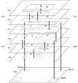
- FIG. 5 is an exploded perspective view of the laminated body when the impedance conversion circuit 35 is configured as a laminated body (multilayer substrate) in which dielectric layers or magnetic layers are laminated.
- FIG. 6 is a diagram showing main magnetic fluxes passing through the coiled conductor by the conductor pattern formed in each layer of the multilayer substrate shown in FIG.
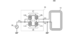
- FIG. 7 is a circuit diagram of the antenna device 102 of the second embodiment.
- FIG. 8 is a circuit diagram of the antenna device 103 according to the third embodiment.
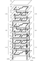
- FIG. 9 is an exploded perspective view of the laminated body in the case where the impedance conversion circuit 45 shown in FIG. 8 is configured as a laminated body in which dielectric layers or magnetic layers are laminated.
- FIG. 10 is a circuit diagram of the antenna device 104 of the fourth embodiment.
- FIG. 11A is a configuration diagram of a communication terminal apparatus as a first example of the fifth embodiment
- FIG. 11B is a configuration diagram of a communication terminal apparatus as a second example.
- FIG. 1A is a circuit diagram of the main part of the impedance conversion circuit 35 included in the antenna device 101 of the first embodiment
- FIG. 1B is a circuit diagram of the antenna device 101.
- the impedance conversion circuit 35 includes a first coiled conductor L1a, a second coiled conductor L1b, a third coiled conductor L2a, and a fourth coiled conductor L2b.
- the first coiled conductor L1a and the second coiled conductor L1b are connected in series to form a first series circuit 26, and the third coiled conductor L2a and the fourth coiled conductor L2b are in series. Is connected to the second series circuit 27.
- the first coiled conductor L1a and the second coiled conductor L1b are a first closed magnetic field in which the first coiled conductor L1a and the second coiled conductor L1b generate a closed loop of the first magnetic flux and are electromagnetically coupled. It is wound to form a road.
- the third coil-shaped conductor L2a and the fourth coil-shaped conductor L2b are electromagnetically coupled by the closed loop of the second magnetic flux generated by the third coil-shaped conductor L2a and the fourth coil-shaped conductor L2b. Two closed magnetic paths are wound.
- the antenna device 101 includes an antenna element 11 and an impedance conversion circuit 35 connected to the antenna element 11.
- the antenna element 11 is a monopole antenna, for example.
- the first terminal P11 of the first series circuit 26 and the first terminal P21 of the second series circuit 27 are connected to the first port P1 of the impedance conversion circuit 35.
- the second terminal P12 of the first series circuit 26 is connected to the second port P2 of the impedance conversion circuit 35.
- the second end P22 of the second series circuit 27 is connected to the third port P3 of the impedance conversion circuit 35.
- the antenna element 11 is connected to the third port P3 of the impedance conversion circuit 35, and the second port P2 is grounded.
- the power feeding circuit 30 is connected to the first port P ⁇ b> 1 of the impedance conversion circuit 35.
- the power supply circuit 30 is a power supply circuit for supplying a high-frequency signal to the antenna element 11 and generates and processes a high-frequency signal, but may include a circuit that combines and demultiplexes the high-frequency signal.
- FIG. 2 is a diagram in which various arrows indicating states of magnetic field coupling and electric field coupling are entered in the circuit illustrated in FIG.
- Capacitors Ca and Cb in FIG. 2 are symbols representing the coupling capacitance for the electric field coupling.
- the first coiled conductor L1a and the second coiled conductor L1b are coupled in phase with each other, and the third coiled conductor L2a and the fourth coiled conductor L2b are coupled in phase with each other to form a closed magnetic circuit. ing. Therefore, the two magnetic fluxes A and B are confined, and between the first coiled conductor L1a and the second coiled conductor L1b, and between the third coiled conductor L2a and the fourth coiled conductor L2b. The loss of energy during can be reduced.
- the inductance values of the first coil-shaped conductor L1a and the second coil-shaped conductor L1b and the inductance values of the third coil-shaped conductor L2a and the fourth coil-shaped conductor L2b are set to substantially the same element value, the closed magnetism The leakage magnetic field on the road is reduced, and the energy loss can be further reduced.
- the impedance conversion ratio can be controlled by appropriately designing the element value of each coiled conductor.
- the magnetic flux A excited by the primary current flowing in the first series circuit 26 and the magnetic flux B excited by the secondary current flowing in the second series circuit 27 are arranged so that the induced magnetic currents repel each other's magnetic flux ( To repel). That is, an equivalent magnetic barrier MW is generated between the first series circuit 26 and the second series circuit 27.
- an equivalent magnetic barrier MW is generated between the first series circuit 26 and the second series circuit 27.
- the first coiled conductor L1a and the third coiled conductor L2a, and the second coiled conductor L1b and the fourth coiled conductor L2b are coupled with a higher degree of coupling. That is, the first series circuit 26 and the second series circuit 27 are coupled with a high degree of coupling.
- FIG. 3A is a circuit diagram obtained by equivalently converting the antenna device 101 of the first embodiment
- FIG. 3B is a circuit diagram obtained by further equivalently converting it.
- the impedance conversion circuit 35E is a diagram showing the impedance conversion circuit 35 shown in FIG. 1B as a simple transformer circuit.
- the inductance of the first series circuit 26 connected to the power feeding circuit 30 shown in FIG. 1B is represented by L1
- the inductance of the second series circuit 27 is represented by L2.
- an impedance conversion circuit 35E is an equivalent conversion of the transformer circuit shown in FIG. 3A into a T-type circuit using inductance elements La, Lb, and Lc.
- the inductance of the inductance element La is (+ M)
- the inductance of the inductance element Lb is (L2-M)
- the inductance of the inductance element Lc is (L1-M). It is.
- L2 ⁇ M
- the inductance (L2-M) of the inductance element Lb is a negative value.
- the antenna element 11 includes an equivalent inductance component LANT, a radiation resistance component Rr, and a capacitance component CANT.
- the inductance component LANT of the antenna element 11 alone acts so as to be canceled out by the negative combined inductance component (L2-M) in the impedance conversion circuit 35E. That is, the inductance component (of the antenna element 11 including the inductance element (L2-M)) viewed from the point A of the impedance conversion circuit 35E is small (ideally zero), and as a result, The impedance frequency characteristic of the antenna device 101 is reduced.
- the impedance conversion ratio by the transformer circuit is L1: (L1 + L2), where L1 represents the inductance of the inductance element L1 and L2 represents the inductance of the inductance element L2.
- FIG. 4 is a diagram schematically showing the action of the negative inductance component that is equivalently generated in the impedance conversion circuit 35 and the action of the impedance conversion circuit 35.
- a curve S0 represents an impedance locus on the Smith chart when the frequency is swept over the use frequency band of the antenna element 11. Since the antenna element 11 alone has a relatively large inductance component LANT, the impedance changes greatly as shown in FIG.
- a curve S1 is an impedance locus when the antenna element 11 side is viewed from the point A of the impedance conversion circuit.
- the inductance component LANT of the antenna element is canceled by the equivalent negative inductance component of the impedance conversion circuit, and the locus of the impedance when the antenna element side is viewed from the point A is greatly reduced.
- a curve S2 is an impedance locus of the antenna device 101 as viewed from the power feeding circuit 30.
- the impedance conversion ratio L1: (L1 + L2) by the transformer-type circuit brings the impedance of the antenna device 101 closer to the impedance of the feeder circuit 30 (the center of the Smith chart).
- This fine adjustment of the impedance may be performed by adding a separate inductance element or capacitance element to the transformer type circuit.
- the impedance change of the antenna device can be suppressed over a wide band. Therefore, impedance matching with the feeder circuit can be achieved over a wide frequency band.
- FIG. 5 is an exploded perspective view of the laminated body when the impedance conversion circuit 35 is configured as a laminated body (multilayer substrate) in which dielectric layers or magnetic layers are laminated.
- each conductor pattern and interlayer connection conductor (via conductor) are drawn through each base material layer.
- the conductor pattern 63 is formed on the base material layer 51a of the laminate, the conductor patterns 62 and 64 are formed on the base material layer 51b, and the conductor patterns 61 and 65 are formed on the base material layer 51c. Yes.
- Conductive patterns 71 and 75 are formed on the base layer 51d, conductive patterns 72 and 74 are formed on the base layer 51e, and conductive patterns 73 are formed on the base layer 51f.
- On the back surface of the base material layer 51g a terminal 41 corresponding to the port P1, a terminal 42 corresponding to the port P2, and a terminal 43 corresponding to the port P3 are formed.
- a plain base material layer (not shown) is laminated on the base material layer 51a.
- the left half of the conductor patterns 61, 62 and 63 constitutes a first coiled conductor L1a
- the right half of the conductor pattern 63, 64 and 65 constitutes a second coiled conductor L1b.
- a third coiled conductor L2a is constituted by the left half of the conductor patterns 71, 72 and 73
- a fourth coiled conductor L2b is constituted by the right half, 74 and 75 of the conductor pattern 73.
- the conductor patterns 61 to 65, 71 to 75 and the terminals 41, 42, and 43 are connected via interlayer connection conductors (via conductors), as shown in FIG. Configure the circuit.
- the first coiled conductor L1a and the second coiled conductor L1b are arranged adjacent to each other so that the winding axes of the respective coil patterns are parallel to each other.
- the third coiled conductor L2a and the fourth coiled conductor L2b are arranged adjacent to each other so that the winding axes of the respective coil patterns are parallel to each other.
- first coiled conductor L1a and the third coiled conductor L2a are arranged close to each other (in a coaxial relationship) so that the winding axes of the respective coil patterns are substantially the same straight line.
- second coiled conductor L1b and the fourth coiled conductor L2b are arranged close to each other (coaxially) so that the winding axes of the respective coil patterns are substantially the same straight line. That is, when viewed from the stacking direction of the base material layers, the conductor patterns constituting each coil pattern are arranged so as to overlap each other.
- each of the coiled conductors L1a, L1b, L2a, and L2b is configured by a loop-shaped conductor having approximately three turns, but the number of turns is not limited thereto.
- the winding axes of the coil patterns of the first coiled conductor L1a and the third coiled conductor L2a do not have to be arranged so as to be exactly the same straight line.
- the coil opening of L1a and the 3rd coiled conductor L2a should just be wound so that it may mutually overlap.
- the coil patterns of the second coil-shaped conductor L1b and the fourth coil-shaped conductor L2b do not have to be arranged so that the winding axes are exactly the same straight line. It is only necessary that the coil openings of the conductor L1b and the fourth coiled conductor L2b are wound so as to overlap each other.
- the various conductor patterns 61 to 65 and 71 to 75 can be formed by screen printing a paste mainly composed of a conductive material such as silver or copper, or etching a metal foil.
- a glass ceramic material, an epoxy resin material or the like can be used if it is a dielectric, and a ferrite ceramic material or a resin material containing ferrite can be used if it is a magnetic material.
- a dielectric material having a high electrical insulation resistance in order to suppress eddy current loss in a high frequency region.
- a magnetic layer may be disposed, and the other layers may be constituted by dielectric layers.
- FIG. 6 shows the main magnetic flux passing through the coiled conductor by the conductor pattern formed in each layer of the multilayer substrate shown in FIG.
- the magnetic flux FP1 passes through the first coiled conductor L1a formed by the conductor patterns 61 to 63 and the second coiled conductor L1b formed by the conductor patterns 63 to 65.
- the magnetic flux FP2 passes through the third coiled conductor L2a formed by the conductor patterns 71 to 73 and the fourth coiled conductor L2b formed by the conductor patterns 73 to 75.
- the coiled conductors L1a, L1b, L2a, and L2b are built in a laminate made of a dielectric material or a magnetic material, and in particular, a region that becomes a coupling portion between the first series circuit and the second series circuit.
- the impedance conversion circuit 35 is hardly affected by other circuits and elements arranged adjacent to the laminated body. As a result, impedance matching can be further stabilized.
- FIG. 7 is a circuit diagram of the antenna device 102 of the second embodiment.
- the antenna device 102 includes an antenna element 12 and an impedance conversion circuit 35 connected to the antenna element 12.
- the antenna element 12 is a loop antenna.
- the first end of the first series circuit 26 and the first end of the second series circuit 27 are connected to the first port P1 of the impedance conversion circuit 35.
- the second end of the first series circuit 26 is connected to the second port P ⁇ b> 2 of the impedance conversion circuit 35.
- the second end of the second series circuit 27 is connected to the third port P3 of the impedance conversion circuit 35.
- the antenna element 12 is connected between the second port P2 and the third port P3 of the impedance conversion circuit 35, and the second port P2 is grounded.
- the power feeding circuit 30 is connected to the first port P ⁇ b> 1 of the impedance conversion circuit 35.
- the power supply circuit 30 is a power supply circuit for supplying a high-frequency signal to the antenna element 11 and generates and processes a high-frequency signal, but may include a circuit that combines and demultiplexes the high-frequency signal.
- the antenna device 102 of the second embodiment is an antenna device for an RFID tag, for example.
- the antenna element 12 is a relatively large loop antenna provided separately from the IC chip for RFID, and the impedance thereof is that of the feeder circuit 30. It is about twice the impedance.
- the impedance conversion ratio of the impedance conversion circuit 35 is 1: 2. Therefore, the power feeding circuit 30 and the antenna element 12 of the antenna device 102 are impedance matched.
- FIG. 8 is a circuit diagram of the antenna device 103 according to the third embodiment.
- the antenna device 103 includes an antenna element 11 and an impedance conversion circuit 45 connected to the antenna element 11.
- the first end of the first series circuit 26, the first end of the second series circuit 27, and the first end of the third series circuit 28 are connected to the first port P1 of the impedance conversion circuit 45, respectively.
- the second end of the first series circuit 26 and the second end of the third series circuit 28 are connected to the second port P2 of the impedance conversion circuit 35.
- the second end of the second series circuit 27 is connected to the third port P3 of the impedance conversion circuit 45.
- the closed loop A of the magnetic flux excited by the primary current flowing in the first series circuit 26 and the closed loop B of the magnetic flux excited by the secondary current flowing in the second series circuit 27 are arranged to repel each other's magnetic flux by the induced current. Occur (to repel each other). That is, an equivalent magnetic barrier MW is generated between the first series circuit 26 and the second series circuit 27.
- the closed loop C of the magnetic flux excited by the primary current flowing in the third series circuit 28 and the closed loop B of the magnetic flux excited by the secondary current flowing in the second series circuit 27 are mutually guided by the induced current. It happens to fit (to repel each other). That is, an equivalent magnetic barrier MW is generated between the third series circuit 28 and the second series circuit 27.
- the closed loop B of the magnetic flux of the central secondary coil has two It is sandwiched between magnetic barriers and sufficiently confined (the confinement effect increases). That is, it can act as a transformer having a larger coupling coefficient.
- FIG. 9 is an exploded perspective view of the laminated body in the case where the impedance conversion circuit 45 shown in FIG. 8 is configured as a laminated body (multilayer substrate) in which dielectric layers or magnetic layers are laminated.
- the base material layers 51a to 51k are made of a dielectric sheet or a magnetic sheet, and a coiled conductor is formed in each layer.
- Conductive pattern 83 is formed on base material layer 51b
- conductive patterns 82 and 84 are formed on base material layer 51c
- conductive patterns 81 and 85 are formed on base material layer 51d
- conductive pattern 73 is formed on base material layer 51e.
- the conductor patterns 72 and 74 are formed on the base material layer 51f, the conductor patterns 71 and 75 are formed on the base material layer 51g, the conductor patterns 61 and 65 are formed on the base material layer 51h, and the conductors are formed on the base material layer 51i. Patterns 62 and 64 are formed, and a conductor pattern 63 is formed on the base material layer 51j. Terminals 41, 42, 43 and the like corresponding to the ports P1, P2, P3 are formed on the lower surface of the base material layer 51k. The lines extending in the vertical direction in FIG. 9 are via electrodes, and the coiled conductors are connected between the layers.
- the first coiled conductor L11a is constituted by the left half of the conductor patterns 61, 62 and the conductor pattern 63
- the second coiled conductor L11b is constituted by the conductor patterns 65, 64 and the right half of the conductor pattern 63.
- the fifth coiled conductor L12a is constituted by the left half of the conductor patterns 81 and 82 and the conductor pattern 83
- the sixth coiled conductor L12b is constituted by the right half of the conductor patterns 85 and 84 and the conductor pattern 83. is doing.
- the third coiled conductor L2a is constituted by the left half of the conductor patterns 71 and 72 and the conductor pattern 73
- the fourth coiled conductor L2b is constituted by the right half of the conductor patterns 75 and 74 and the conductor pattern 73. is doing.
- FIG. 10 is a circuit diagram of the antenna device 104 of the fourth embodiment.
- the antenna device 104 includes an antenna element 11 and an impedance conversion circuit 55 connected to the antenna element 11.
- the first end of the first series circuit 26, the first end of the second series circuit 27, and the first end of the third series circuit 28 are connected to the first port P1 of the impedance conversion circuit 55, respectively.
- the second end of the first series circuit 26 is connected to the second port P ⁇ b> 2 of the impedance conversion circuit 55.
- the second end of the second series circuit 27 and the second end of the third series circuit 28 are connected to the third port P3 of the impedance conversion circuit 55.
- the closed loop A of the magnetic flux excited by the primary current flowing in the first series circuit 26 and the closed loop B of the magnetic flux excited by the secondary current flowing in the second series circuit 27 are arranged to repel each other's magnetic flux by the induced current. Occur (to repel each other). That is, an equivalent magnetic barrier MW is generated between the first series circuit 26 and the second series circuit 27.
- the closed loop A of the magnetic flux excited by the primary current flowing in the first series circuit 26 and the closed loop C of the magnetic flux excited by the secondary current flowing in the third series circuit 28 screen each other's magnetic flux by the induced current. It happens to fit (to repel each other). That is, an equivalent magnetic barrier MW is generated between the first series circuit 26 and the third series circuit 28.
- the closed loop A of the magnetic flux of the central primary coil is divided into two magnets. It is sandwiched by barriers and sufficiently confined (the confinement effect increases). That is, it can act as a transformer having a very large coupling coefficient.
- FIG. 11 is an RFID system circuit diagram of the fifth embodiment which is an example of the communication terminal device of the present invention.
- the RFID tag 106 includes an antenna element 12 that is a loop antenna, an impedance conversion circuit 35, an RFIC 91, and a baseband IC 92.
- the reader / writer 105 includes a reader / writer control circuit 93, an impedance conversion circuit 25, and an antenna element 13 that is a loop antenna.
- the wireless IC chip 70 includes an RFIC that constitutes a high-frequency circuit and a baseband IC that constitutes a logic circuit. As the impedance conversion circuits 25 and 35, the impedance conversion circuit shown in any one of the first to fourth embodiments is applied.
- the impedance of the antenna element 12 is higher than the impedance of the antenna-side port of the RFIC, and the impedance conversion circuit 35 matches the impedance of both.
- the impedance of the antenna element 13 is higher than the impedance of the antenna side port of the reader / writer control circuit 93, and the impedance conversion circuit 25 matches the impedance of both.
- the impedance of the antenna elements 12 and 13 is likely to change.
- the impedance matching state is stabilized by providing the impedance conversion circuits 25 and 35. be able to. That is, it becomes possible for the impedance conversion circuits 25 and 35 to perform frequency characteristic adjustment functions such as center frequency setting, passband width setting, and impedance matching setting, which are important matters regarding antenna design. Since the elements 12 and 13 need only mainly consider directivity and gain, antenna design is facilitated.
- second port P3 ... third port Rr antenna radiation Resistance component 10, 20 ... Housing 11 ... Antenna element 12 ... Antenna element 26 ... First series circuit 27 ... Second series circuit 28 ... third series circuit 30 ... feed circuit 35, 35E ... impedance conversion circuits 41, 42, 43 ... terminal 45 ... impedance conversion circuits 51a to 51k ... base material layer 55 ... impedance conversion circuits 61 to 65 ... conductor pattern 71 ... 75 ... Conductor patterns 81 to 85 ... Conductor patterns 101 to 104 ... Antenna device
Landscapes
- Engineering & Computer Science (AREA)
- Computer Networks & Wireless Communication (AREA)
- Signal Processing (AREA)
- Details Of Aerials (AREA)
- Near-Field Transmission Systems (AREA)
- Filters And Equalizers (AREA)
- Input Circuits Of Receivers And Coupling Of Receivers And Audio Equipment (AREA)
Abstract
アンテナ装置(101)は、アンテナ素子(11)と、このアンテナ素子(11)に接続されたインピーダンス変換回路(35)とを備えている。インピーダンス変換回路(35)はアンテナ素子(11)と給電回路(30)との間に挿入される。インピーダンス変換回路(35)は、第1のコイル状導体(L1a)と第2のコイル状導体(L1b)とが直列に接続された第1の直列回路(26)、および、第3のコイル状導体(L2a)と第4のコイル状導体(L2b)とが直列に接続された第2の直列回路(27)を備えている。第1のコイル状導体(L1a)および第2のコイル状導体(L1b)は、第1の磁束の閉ループが通る閉磁路を構成し、第3のコイル状導体(L2a)および第4のコイル状導体(L2b)は第2の磁束の閉ループが通る閉磁路を構成している。これにより、アンテナ装置広い周波数帯域で給電回路とインピーダンス整合する。
Description
本発明は、インピーダンス変換回路を備えたアンテナ装置およびこれを用いた通信端末装置に関し、特に、広い周波数帯域でインピーダンス整合するアンテナ装置および通信端末装置に関する。
近年、携帯電話をはじめとする通信端末装置は、GSM(登録商標)(Global System for mobile Communications)、DCS(Digital CommunicationSystem)、PCS(PersonalCommunication Services)、UMTS(Universal Mobile Telecommunications System)等の通信システム、さらにはGPS(GlobalPositioning system)やワイヤレスLAN、Bluetooth(登録商標)等への対応が求められることがある。したがって、こうした通信端末装置におけるアンテナ装置は、800MHz~2.4GHzまでの広い周波数帯域をカバーすることが求められる。
広い周波数帯域に対応するアンテナ装置としては、特許文献1や特許文献2に開示されているように、LC並列共振回路やLC直列共振回路にて構成された広帯域の整合回路を備えたものが一般的である。また、広い周波数帯域に対応するアンテナ装置として、例えば特許文献3や特許文献4に開示されているようなチューナブルアンテナが知られている。
ところが、特許文献1,2に示されている整合回路は複数の共振回路を含むものであるため、この整合回路における挿入損失が大きくなりやすく、十分な利得が得られないことがある。
他方、特許文献3,4に示されているチューナブルアンテナは、可変容量素子を制御するための回路、すなわち周波数帯域を切り換えるための切替回路、が必要であるので回路構成が複雑になりやすい。また、切替回路での損失や歪みが大きいので十分な利得が得られないことがある。
本発明は上述した実情に鑑みてなされたものであり、その目的は、広い周波数帯域で給電回路とインピーダンス整合するアンテナ装置、およびこのアンテナ装置を備えた通信端末装置を提供することにある。
(1)本発明のアンテナ装置は、アンテナ素子と、このアンテナ素子に接続されたインピーダンス変換回路とを含むアンテナ装置であって、
前記インピーダンス変換回路は、第1インダクタンス素子と第2インダクタンス素子とが相互インダクタンスを介して結合されたトランス型回路を含み、
前記第1インダクタンス素子の第1端は給電回路に、第2端はグランドにそれぞれ接続されていて、
前記第2インダクタンス素子の第1端は前記給電回路に、第2端は前記アンテナ素子にそれぞれ接続されていて、
前記相互インダクタンスは、前記第2インダクタンス素子のインダクタンスより大きいことを特徴とする。
前記インピーダンス変換回路は、第1インダクタンス素子と第2インダクタンス素子とが相互インダクタンスを介して結合されたトランス型回路を含み、
前記第1インダクタンス素子の第1端は給電回路に、第2端はグランドにそれぞれ接続されていて、
前記第2インダクタンス素子の第1端は前記給電回路に、第2端は前記アンテナ素子にそれぞれ接続されていて、
前記相互インダクタンスは、前記第2インダクタンス素子のインダクタンスより大きいことを特徴とする。
(2)前記第1インダクタンス素子は第1のコイル状導体および第2のコイル状導体を備え、前記第2インダクタンス素子は第3のコイル状導体および第4のコイル状導体を備え、
前記第1のコイル状導体および前記第2のコイル状導体は、前記第1のコイル状導体と前記第2のコイル状導体とによって第1の磁束の閉ループが生じて電磁界結合するように巻回されていて、
前記第3のコイル状導体および前記第4のコイル状導体は、前記第3のコイル状導体と前記第4のコイル状導体とによって第2の磁束の閉ループが生じて電磁界結合するように巻回されていることが好ましい。
前記第1のコイル状導体および前記第2のコイル状導体は、前記第1のコイル状導体と前記第2のコイル状導体とによって第1の磁束の閉ループが生じて電磁界結合するように巻回されていて、
前記第3のコイル状導体および前記第4のコイル状導体は、前記第3のコイル状導体と前記第4のコイル状導体とによって第2の磁束の閉ループが生じて電磁界結合するように巻回されていることが好ましい。
(3)(2) において、前記第1のコイル状導体、前記第2のコイル状導体、前記第3のコイル状導体、および前記第4のコイル状導体は、前記第1の磁束の閉ループを回る磁束(第1の閉磁路を通る磁束)と前記第2の磁束の閉ループを回る磁束(第2の閉磁路を通る磁束)とが互いに逆方向になるように巻回されていることが好ましい。
(4)(2) または(3) において、前記第1のコイル状導体および前記第3のコイル状導体は互いに磁界および電界を介して結合し、
前記第2のコイル状導体および前記第4のコイル状導体は互いに磁界および電界を介して結合し、
前記第1インダクタンス素子に交流電流が流れるとき、前記磁界を介した結合により前記第2インダクタンス素子に流れる電流の向きと、前記電界を介した結合により前記第2の直列回路に流れる電流の向きとが同じであることが好ましい。
前記第2のコイル状導体および前記第4のコイル状導体は互いに磁界および電界を介して結合し、
前記第1インダクタンス素子に交流電流が流れるとき、前記磁界を介した結合により前記第2インダクタンス素子に流れる電流の向きと、前記電界を介した結合により前記第2の直列回路に流れる電流の向きとが同じであることが好ましい。
(5)また、(2)~(4) のいずれかにおいて、前記第1のコイル状導体、前記第2のコイル状導体、前記第3のコイル状導体、および前記第4のコイル状導体は複数の誘電体層または磁性体層が積層された積層体内の導体パターンで構成されていることが好ましい。
(6)(5) において、前記第1のコイル状導体、前記第2のコイル状導体、前記第3のコイル状導体、および前記第4のコイル状導体のそれぞれの巻回軸は前記積層体の積層方向に向き、
前記第1のコイル状導体と第2のコイル状導体は、それぞれの巻回軸が異なる関係で並置され、
前記第3のコイル状導体と第4のコイル状導体は、それぞれの巻回軸が異なる関係で並置され、
前記第1のコイル状導体と第3のコイル状導体のそれぞれの巻回範囲が平面視で少なくとも一部で重なり、前記第2のコイル状導体と第4のコイル状導体のそれぞれの巻回範囲が平面視で少なくとも一部で重なっていることが好ましい。
前記第1のコイル状導体と第2のコイル状導体は、それぞれの巻回軸が異なる関係で並置され、
前記第3のコイル状導体と第4のコイル状導体は、それぞれの巻回軸が異なる関係で並置され、
前記第1のコイル状導体と第3のコイル状導体のそれぞれの巻回範囲が平面視で少なくとも一部で重なり、前記第2のコイル状導体と第4のコイル状導体のそれぞれの巻回範囲が平面視で少なくとも一部で重なっていることが好ましい。
(7)(2)~(6) のいずれかにおいて、前記インピーダンス変換回路は、第5のコイル状導体および第6のコイル状導体をさらに備え、
第5のコイル状導体と第6のコイル状導体とが直列に接続されて第3インダクタンス素子が構成され、
第5のコイル状導体および第6のコイル状導体は、第5のコイル状導体と第6のコイル状導体とによって第3の磁束の閉ループが生じて電磁界結合する(第3の閉磁路が構成される)ように巻回されていて、
前記第3インダクタンス素子の第1端は前記給電回路に接続され、前記第3インダクタンス素子の第2端は前記グランドに接続され、
前記第1のコイル状導体、前記第2のコイル状導体、前記第3のコイル状導体、前記第4のコイル状導体、第5のコイル状導体および前記第6のコイル状導体は、前記第2の磁束の閉ループを回る磁束が第1の磁束の閉ループを回る磁束および第3の磁束の閉ループを回る磁束で挟み込まれるように配置されていることが好ましい。
第5のコイル状導体と第6のコイル状導体とが直列に接続されて第3インダクタンス素子が構成され、
第5のコイル状導体および第6のコイル状導体は、第5のコイル状導体と第6のコイル状導体とによって第3の磁束の閉ループが生じて電磁界結合する(第3の閉磁路が構成される)ように巻回されていて、
前記第3インダクタンス素子の第1端は前記給電回路に接続され、前記第3インダクタンス素子の第2端は前記グランドに接続され、
前記第1のコイル状導体、前記第2のコイル状導体、前記第3のコイル状導体、前記第4のコイル状導体、第5のコイル状導体および前記第6のコイル状導体は、前記第2の磁束の閉ループを回る磁束が第1の磁束の閉ループを回る磁束および第3の磁束の閉ループを回る磁束で挟み込まれるように配置されていることが好ましい。
(8)(2)~(6) のいずれかにおいて、前記インピーダンス変換回路は、第5のコイル状導体および第6のコイル状導体をさらに備え、
第5のコイル状導体と第6のコイル状導体とが直列に接続されて第3インダクタンス素子が構成され、
第5のコイル状導体および第6のコイル状導体は、第5のコイル状導体と第6のコイル状導体とによって第3の磁束の閉ループが生じて電磁界結合する(第3の閉磁路が構成される)ように巻回されていて、
前記第3インダクタンス素子の第1端は前記給電回路に接続され、前記第3インダクタンス素子の第2端は前記グランドに接続され、
前記第1のコイル状導体、前記第2のコイル状導体、前記第3のコイル状導体、前記第4のコイル状導体および前記第5のコイル状導体は、前記第1の磁束の閉ループを回る磁束が第2の磁束の閉ループを回る磁束および第3の磁束の閉ループを回る磁束で層方向に挟み込まれるように配置されていることが好ましい。
第5のコイル状導体と第6のコイル状導体とが直列に接続されて第3インダクタンス素子が構成され、
第5のコイル状導体および第6のコイル状導体は、第5のコイル状導体と第6のコイル状導体とによって第3の磁束の閉ループが生じて電磁界結合する(第3の閉磁路が構成される)ように巻回されていて、
前記第3インダクタンス素子の第1端は前記給電回路に接続され、前記第3インダクタンス素子の第2端は前記グランドに接続され、
前記第1のコイル状導体、前記第2のコイル状導体、前記第3のコイル状導体、前記第4のコイル状導体および前記第5のコイル状導体は、前記第1の磁束の閉ループを回る磁束が第2の磁束の閉ループを回る磁束および第3の磁束の閉ループを回る磁束で層方向に挟み込まれるように配置されていることが好ましい。
(9)本発明の通信端末装置は、アンテナ素子と、給電回路と、前記アンテナ素子と前記給電回路との間に接続されたインピーダンス変換回路とを含むアンテナ装置を備え、
前記インピーダンス変換回路は、第1のコイル状導体、第2のコイル状導体、第3のコイル状導体、第4のコイル状導体を少なくとも備え、
前記インピーダンス変換回路は、第1インダクタンス素子と第2インダクタンス素子とが相互インダクタンスを介して結合されたトランス型回路を含み、
前記第1インダクタンス素子の第1端は給電回路に、第2端はグランドにそれぞれ接続されていて、
前記第2インダクタンス素子の第1端は前記給電回路に、第2端は前記アンテナ素子にそれぞれ接続されていて、
前記相互インダクタンスは、前記第2インダクタンス素子のインダクタンスより大きいことを特徴とする。
前記インピーダンス変換回路は、第1のコイル状導体、第2のコイル状導体、第3のコイル状導体、第4のコイル状導体を少なくとも備え、
前記インピーダンス変換回路は、第1インダクタンス素子と第2インダクタンス素子とが相互インダクタンスを介して結合されたトランス型回路を含み、
前記第1インダクタンス素子の第1端は給電回路に、第2端はグランドにそれぞれ接続されていて、
前記第2インダクタンス素子の第1端は前記給電回路に、第2端は前記アンテナ素子にそれぞれ接続されていて、
前記相互インダクタンスは、前記第2インダクタンス素子のインダクタンスより大きいことを特徴とする。
本発明によれば、整合回路における挿入損失が小さく、周波数帯域を切り換えるための切替回路も不要であり、広い周波数帯域に亘って給電回路とインピーダンス整合するアンテナ装置およびそれを備えた通信端末装置が構成できる。
また、本発明の通信端末装置によれば、前記のアンテナ装置を用いているため、周波数帯域の異なる各種の通信システムに対応可能な通信端末装置を実現できる。
《第1の実施形態》
図1(A)は第1の実施形態のアンテナ装置101が含むインピーダンス変換回路35の主要部の回路図、図1(B)はアンテナ装置101の回路図である。
図1(A)に示すようにインピーダンス変換回路35は、第1のコイル状導体L1a、第2のコイル状導体L1b、第3のコイル状導体L2a、第4のコイル状導体L2bを備えている。第1のコイル状導体L1aと第2のコイル状導体L1bとは直列に接続されて第1の直列回路26が構成され、第3のコイル状導体L2aと第4のコイル状導体L2bとは直列に接続されて第2の直列回路27が構成されている。
図1(A)は第1の実施形態のアンテナ装置101が含むインピーダンス変換回路35の主要部の回路図、図1(B)はアンテナ装置101の回路図である。
図1(A)に示すようにインピーダンス変換回路35は、第1のコイル状導体L1a、第2のコイル状導体L1b、第3のコイル状導体L2a、第4のコイル状導体L2bを備えている。第1のコイル状導体L1aと第2のコイル状導体L1bとは直列に接続されて第1の直列回路26が構成され、第3のコイル状導体L2aと第4のコイル状導体L2bとは直列に接続されて第2の直列回路27が構成されている。
第1のコイル状導体L1aおよび第2のコイル状導体L1bは第1のコイル状導体L1aと第2のコイル状導体L1bとによって第1の磁束の閉ループが生じて電磁界結合する第1の閉磁路が構成されるように巻回されている。同様に、第3のコイル状導体L2aおよび第4のコイル状導体L2bは第3のコイル状導体L2aと第4のコイル状導体L2bとによって第2の磁束の閉ループが生じて電磁界結合する第2の閉磁路が構成されるように巻回されている。
図1(B)に示すように、アンテナ装置101は、アンテナ素子11と、このアンテナ素子11に接続されたインピーダンス変換回路35とを備えている。アンテナ素子11は例えばモノポール型アンテナである。第1の直列回路26の第1端P11および第2の直列回路27の第1端P21はインピーダンス変換回路35の第1ポートP1に接続されている。第1の直列回路26の第2端P12はインピーダンス変換回路35の第2ポートP2に接続されている。また、第2の直列回路27の第2端P22はインピーダンス変換回路35の第3ポートP3に接続されている。
インピーダンス変換回路35の第3ポートP3にはアンテナ素子11が接続されていて、第2ポートP2はグランドに接地されている。インピーダンス変換回路35の第1ポートP1には給電回路30が接続される。この給電回路30は高周波信号をアンテナ素子11に給電するための給電回路であり、高周波信号の生成や処理を行うが、高周波信号の合波や分波を行う回路を含んでいてもよい。
図2は図1(B)に示した回路に磁界結合と電界結合の様子を示す各種矢印を書き入れた図である。
図2に示すように、給電回路30から図中矢印a方向に電流が供給されたとき、第1のコイル状導体L1aに図中矢印b方向に電流が流れるとともに、コイル状導体L1bには図中矢印c方向に電流が流れる。そして、これらの電流により、図中矢印Aで示される磁束(閉磁路を通る磁束)が形成される。
ここで、第1のコイル状導体L1aと第3のコイル状導体L2aとは、コイル巻回軸を共有するように、かつ平面視した状態でコイル導体パターンが並走しているので、両者間に電界結合が発生し、この電界結合によって流れる電流は前記誘導電流と同じ方向に流れる。すなわち、磁界結合と電界結合とで結合度を強めている。同様に第2のコイル状導体L1bと第4のコイル状導体L2bとでも磁界結合と電界結合が生じる。図2中のキャパシタCa,Cbは前記電界結合のための結合容量を表象的に表した記号である。
第1のコイル状導体L1aおよび第2のコイル状導体L1bは互いに同相で結合し、第3のコイル状導体L2aおよび第4のコイル状導体L2bは互いに同相で結合し、それぞれ閉磁路を形成している。そのため、前記二つの磁束A,Bが閉じ込められて、第1のコイル状導体L1aと第2のコイル状導体L1bとの間、並びに第3のコイル状導体L2aと第4のコイル状導体L2bとの間のエネルギーの損失を小さくすることができる。なお、第1のコイル状導体L1aおよび第2のコイル状導体L1bのインダクタンス値、第3のコイル状導体L2aおよび第4のコイル状導体L2bのインダクタンス値を実質的に同じ素子値にすると、閉磁路の漏れ磁界が少なくなり、エネルギーの損失をより小さくすることができる。もちろん、各コイル状導体の素子値を適宜設計して、インピーダンス変換比をコントロールすることができる。
また、第1の直列回路26に流れる一次電流によって励起される磁束Aと、第2の直列回路27に流れる二次電流によって励起される磁束Bは誘導電流によって互いの磁束をしりぞけ合うように(反発しあうように)生じる。すなわち第1の直列回路26と第2の直列回路27との間には等価的な磁気障壁MWが生じることになる。その結果、第1のコイル状導体L1aおよび第2のコイル状導体L1bに生じる磁界と第3のコイル状導体L2aおよび第4のコイル状導体L2bに生じる磁界とが、それぞれ狭空間に閉じ込められるので、第1のコイル状導体L1aおよび第3のコイル状導体L2a、並びに第2のコイル状導体L1bおよび第4のコイル状導体L2bは、それぞれより高い結合度で結合する。すなわち、第1の直列回路26と第2の直列回路27とは高い結合度で結合する。
図3(A)は第1の実施形態のアンテナ装置101を等価変換した回路図、図3(B)はそれをさらに等価変換した回路図である。
インピーダンス変換回路35Eは図1(B)に示したインピーダンス変換回路35を単純なトランス回路として表した図である。ここでは、図1(B)に示した給電回路30に接続された第1の直列回路26のインダクタンスをL1、第2の直列回路27のインダクタンスをL2で表している。
インピーダンス変換回路35Eは図1(B)に示したインピーダンス変換回路35を単純なトランス回路として表した図である。ここでは、図1(B)に示した給電回路30に接続された第1の直列回路26のインダクタンスをL1、第2の直列回路27のインダクタンスをL2で表している。
図3(B)において、インピーダンス変換回路35Eは図3(A)に示したトランス回路をインダクタンス素子La,Lb,LcによるT型回路に等価変換した図である。ここで前記インダクタンスL1とL2との相互インダクタンスをMで表すと、インダクタンス素子Laのインダクタンスは(+M)、インダクタンス素子Lbのインダクタンスは(L2-M)、インダクタンス素子Lcのインダクタンスは(L1-M)である。ここで、L2<Mの関係とすれば、インダクタンス素子Lbのインダクタンス(L2-M)は負の値となる。
アンテナ素子11は、等価的なインダクタンス成分LANT、放射抵抗成分Rr、およびキャパシタンス成分CANTで構成される。このアンテナ素子11単体のインダクタンス成分LANTは、インピーダンス変換回路35Eにおける負の合成インダクタンス成分(L2-M)によって打ち消されるように作用する。すなわち、インピーダンス変換回路35EのA点からアンテナ素子11側を見た(インダクタンス素子(L2-M)を含めたアンテナ素子11の)インダクタンス成分は小さく(理想的にはゼロに)なり、その結果、このアンテナ装置101のインピーダンス周波数特性が小さくなる。
このように負のインダクタンス成分を生じさせるためには、第1インダクタンス素子と第2インダクタンス素子とを高い結合度で結合させることが重要である。
トランス型回路によるインピーダンス変換比は、インダクタンス素子L1のインダクタンスをL1、インダクタンス素子L2のインダクタンスをL2で表すと、L1:(L1+L2)である。
図4は前記インピーダンス変換回路35で等価的に生じる負のインダクタンス成分の作用およびインピーダンス変換回路35の作用を模式的に示す図である。図4において曲線S0はアンテナ素子11の使用周波数帯域に亘って周波数をスイープしたときのインピーダンス軌跡をスミスチャート上に表したものである。アンテナ素子11単体ではインダクタンス成分LANTが比較的大きいので、図4に表れているようにインピーダンスは大きく推移する。
図4において曲線S1はインピーダンス変換回路のA点からアンテナ素子11側を見たインピーダンスの軌跡である。このように、インピーダンス変換回路の等価的な負のインダクタンス成分によってアンテナ素子のインダクタンス成分LANTが相殺されて、A点からアンテナ素子側を見たインピーダンスの軌跡は大幅に縮小される。
図4において曲線S2は給電回路30から見たインピーダンスすなわちアンテナ装置101のインピーダンスの軌跡である。このように、トランス型回路によるインピーダンス変換比L1:(L1+L2)によって、アンテナ装置101のインピーダンスは給電回路30のインピーダンス(スミスチャートの中心)に近づく。なお、このインピーダンスの微調整は、トランス型回路に、別途インダクタンス素子やキャパシタンス素子を付加することで行ってもよい。
このようにして、広帯域に亘ってアンテナ装置のインピーダンス変化を抑制できる。ゆえに、広い周波数帯域に亘って給電回路とインピーダンス整合がとれる。
図5はインピーダンス変換回路35を誘電体層または磁性体層が積層された積層体(多層基板)に構成した場合の、その積層体の分解斜視図である。図5においては、各基材層を透視して各導体パターンおよび層間接続導体(ビア導体)を描いている。
図5に示すように、積層体の基材層51aに導体パターン63が形成され、基材層51bに導体パターン62,64が形成され、基材層51cに導体パターン61,65が形成されている。また、基材層51dに導体パターン71,75が形成され、基材層51eに導体パターン72,74が形成され、基材層51fに導体パターン73が形成されている。基材層51gの裏面には、ポートP1に相当する端子41、ポートP2に相当する端子42、ポートP3に相当する端子43が形成されている。なお、基材層51a上には図示しない無地の基材層が積層される。
前記導体パターン61,62および63の左半分によって第1のコイル状導体L1aが構成されていて、前記導体パターン63の右半分、64および65によって第2のコイル状導体L1bが構成されている。また、前記導体パターン71,72および73の左半分によって第3のコイル状導体L2aが構成されていて、前記導体パターン73の右半分、74および75によって第4のコイル状導体L2bが構成されている。
前記基材層51a~51gを積層することで、導体パターン61~65,71~75および端子41,42,43は層間接続導体(ビア導体)を介して接続され、図1(B)に示す回路を構成する。
図5に示すように、第1のコイル状導体L1aと第2のコイル状導体L1bは、それぞれのコイルパターンの巻回軸が互いに平行になるように隣接配置されている。同様に第3のコイル状導体L2aと第4のコイル状導体L2bは、それぞれのコイルパターンの巻回軸が互いに平行になるように隣接配置されている。さらに、第1のコイル状導体L1aと第3のコイル状導体L2aは、それぞれのコイルパターンの巻回軸がほぼ同一直線になるように(同軸関係に)近接配置されている。同様に、第2のコイル状導体L1bと第4のコイル状導体L2bは、それぞれのコイルパターンの巻回軸がほぼ同一直線になるように(同軸関係に)近接配置されている。すなわち、基材層の積層方向からみたとき、各コイルパターンを構成する導体パターンは重なるように配置されている。
図5に示すように、第1のコイル状導体L1aと第2のコイル状導体L1bは、それぞれのコイルパターンの巻回軸が互いに平行になるように隣接配置されている。同様に第3のコイル状導体L2aと第4のコイル状導体L2bは、それぞれのコイルパターンの巻回軸が互いに平行になるように隣接配置されている。さらに、第1のコイル状導体L1aと第3のコイル状導体L2aは、それぞれのコイルパターンの巻回軸がほぼ同一直線になるように(同軸関係に)近接配置されている。同様に、第2のコイル状導体L1bと第4のコイル状導体L2bは、それぞれのコイルパターンの巻回軸がほぼ同一直線になるように(同軸関係に)近接配置されている。すなわち、基材層の積層方向からみたとき、各コイルパターンを構成する導体パターンは重なるように配置されている。
なお、各コイル状導体L1a,L1b,L2a,L2bはそれぞれほぼ3ターンのループ状導体にて構成されているが、ターン数はこれに限らない。また、第1のコイル状導体L1aおよび第3のコイル状導体L2aのコイルパターンの巻回軸は厳密に同一直線になるように配置されている必要はなく、平面視で第1のコイル状導体L1aおよび第3のコイル状導体L2aのコイル開口が互いに重なるように巻回されていればよい。同様に、第2のコイル状導体L1bおよび第4のコイル状導体L2bのコイルパターンは巻回軸が厳密に同一直線になるように配置されている必要はなく、平面視で第2のコイル状導体L1bおよび第4のコイル状導体L2bのコイル開口が互いに重なるように巻回されていればよい。
前記各種導体パターン61~65,71~75には、銀や銅などの導電性材料を主成分とするペーストのスクリーン印刷や、金属箔のエッチングなどで形成することができる。基材層51a~51gには、誘電体であればガラスセラミック材料、エポキシ系樹脂材料などを用いることができ、磁性体であればフェライトセラミック材料やフェライトを含有する樹脂材料などを用いることができる。基材層用の材料としては、特に、UHF帯用のインピーダンス変換回路を形成する場合は、高周波数領域での渦電流損失を抑えるために、電気絶縁抵抗の高い誘電体材料を用いることが好ましい。HF帯用のコモンモードチョークコイルを形成する場合は渦電流損失が相対的に小さいので、磁気エネルギーの閉じ込め性の点で、磁性体材料(透磁率の高い誘電体材料)を用いることが好ましい。
なお、第1のコイル素子L1aおよび第2のコイル素子L1bを構成する導体パターン61~65と、第3のコイル素子L2aおよび第4のコイル素子L2bを構成する導体パターン71~75との間に磁性体層を配置し、その他の層を誘電体層で構成してもよい。このことにより、渦電流損失を殆ど増大させることなく、第1コイル素子L1aと第2コイル素子L1bとの磁気的結合および第3コイル素子L2aと第4コイル素子L2bとの磁気的結合を高めることができる。
図6は図5に示した多層基板の各層に形成された導体パターンによるコイル状導体を通る主な磁束を示している。磁束FP1は導体パターン61~63による第1のコイル状導体L1aおよび導体パターン63~65による第2のコイル状導体L1bを通る。また、磁束FP2は導体パターン71~73による第3のコイル状導体L2aおよび導体パターン73~75による第4のコイル状導体L2bを通る。
以上のごとく、コイル状導体L1a,L1b,L2a,L2bを誘電体や磁性体からなる積層体に内蔵すること、特に、第1の直列回路と第2の直列回路との結合部となる領域を積層体の内部に設けることによって、インピーダンス変換回路35が積層体に隣接して配置される他の回路や素子からの影響を受けにくくなる。その結果、インピーダンス整合の一層の安定化を図ることができる。
《第2の実施形態》
図7は第2の実施形態のアンテナ装置102の回路図である。図7に示すように、アンテナ装置102は、アンテナ素子12と、このアンテナ素子12に接続されたインピーダンス変換回路35とを備えている。アンテナ素子12はループアンテナである。第1の直列回路26の第1端および第2の直列回路27の第1端はインピーダンス変換回路35の第1ポートP1に接続されている。第1の直列回路26の第2端はインピーダンス変換回路35の第2ポートP2に接続されている。また、第2の直列回路27の第2端はインピーダンス変換回路35の第3ポートP3に接続されている。
図7は第2の実施形態のアンテナ装置102の回路図である。図7に示すように、アンテナ装置102は、アンテナ素子12と、このアンテナ素子12に接続されたインピーダンス変換回路35とを備えている。アンテナ素子12はループアンテナである。第1の直列回路26の第1端および第2の直列回路27の第1端はインピーダンス変換回路35の第1ポートP1に接続されている。第1の直列回路26の第2端はインピーダンス変換回路35の第2ポートP2に接続されている。また、第2の直列回路27の第2端はインピーダンス変換回路35の第3ポートP3に接続されている。
インピーダンス変換回路35の第2ポートP2と第3ポートP3との間にアンテナ素子12が接続されていて、第2ポートP2はグランドに接地されている。インピーダンス変換回路35の第1ポートP1には給電回路30が接続される。この給電回路30は高周波信号をアンテナ素子11に給電するための給電回路であり、高周波信号の生成や処理を行うが、高周波信号の合波や分波を行う回路を含んでいてもよい。
この第2の実施形態のアンテナ装置102は例えばRFIDタグ用のアンテナ装置であり、アンテナ素子12はRFID用ICチップとは別に設けられた比較的大きなループアンテナであり、そのインピーダンスは給電回路30のインピーダンスの約2倍である。また、インピーダンス変換回路35のインピーダンス変換比は1:2である。そのため、このアンテナ装置102の給電回路30とアンテナ素子12はインピーダンス整合する。
《第3の実施形態》
図8は第3の実施形態のアンテナ装置103の回路図である。図8に示すように、アンテナ装置103は、アンテナ素子11と、このアンテナ素子11に接続されたインピーダンス変換回路45とを備えている。第1の直列回路26の第1端、第2の直列回路27の第1端および第3の直列回路28の第1端はインピーダンス変換回路45の第1ポートP1にそれぞれ接続されている。第1の直列回路26の第2端および第3の直列回路28の第2端はインピーダンス変換回路35の第2ポートP2に接続されている。また、第2の直列回路27の第2端はインピーダンス変換回路45の第3ポートP3に接続されている。
図8は第3の実施形態のアンテナ装置103の回路図である。図8に示すように、アンテナ装置103は、アンテナ素子11と、このアンテナ素子11に接続されたインピーダンス変換回路45とを備えている。第1の直列回路26の第1端、第2の直列回路27の第1端および第3の直列回路28の第1端はインピーダンス変換回路45の第1ポートP1にそれぞれ接続されている。第1の直列回路26の第2端および第3の直列回路28の第2端はインピーダンス変換回路35の第2ポートP2に接続されている。また、第2の直列回路27の第2端はインピーダンス変換回路45の第3ポートP3に接続されている。
第1の直列回路26に流れる一次電流によって励起される磁束の閉ループAと、第2の直列回路27に流れる二次電流によって励起される磁束の閉ループBは誘導電流によって互いの磁束をしりぞけ合うように(反発しあうように)生じる。すなわち第1の直列回路26と第2の直列回路27との間には等価的な磁気障壁MWが生じることになる。
また、第3の直列回路28に流れる一次電流によって励起される磁束の閉ループCと、第2の直列回路27に流れる二次電流によって励起される磁束の閉ループBは誘導電流によって互いの磁束をしりぞけ合うように(反発しあうように)生じる。すなわち第3の直列回路28と第2の直列回路27との間には等価的な磁気障壁MWが生じることになる。
このように、中央の二次側コイルの磁束の閉ループBを上下の一次側コイルの磁束の閉ループA,Cで挟み込んだ構造によれば、中央の二次側コイルの磁束の閉ループBは二つの磁気障壁で挟まれて充分に閉じ込められる(閉じ込められる効果が高まる)。すなわち、結合係数のより大きなトランスとして作用させることができる。
図9は、図8に示したインピーダンス変換回路45を誘電体層または磁性体層が積層された積層体(多層基板)に構成した場合の、その積層体の分解斜視図である。
図9に示すように、基材層51a~51kは誘電体シートまたは磁性体シートで構成され、各層にコイル状導体が形成されている。基材層51bに導体パターン83が形成され、基材層51cに導体パターン82,84が形成され、基材層51dに導体パターン81,85が形成され、基材層51eに導体パターン73が形成され、基材層51fに導体パターン72,74が形成され、基材層51gに導体パターン71,75が形成され、基材層51hに導体パターン61,65が形成され、基材層51iに導体パターン62,64が形成され、基材層51jに導体パターン63が形成されている。基材層51kの下面には、ポートP1,P2,P3に相当する端子41,42,43等が形成されている。図9中の縦方向に延びる線はビア電極であり、コイル状導体同士を層間で接続する。
図9に示すように、基材層51a~51kは誘電体シートまたは磁性体シートで構成され、各層にコイル状導体が形成されている。基材層51bに導体パターン83が形成され、基材層51cに導体パターン82,84が形成され、基材層51dに導体パターン81,85が形成され、基材層51eに導体パターン73が形成され、基材層51fに導体パターン72,74が形成され、基材層51gに導体パターン71,75が形成され、基材層51hに導体パターン61,65が形成され、基材層51iに導体パターン62,64が形成され、基材層51jに導体パターン63が形成されている。基材層51kの下面には、ポートP1,P2,P3に相当する端子41,42,43等が形成されている。図9中の縦方向に延びる線はビア電極であり、コイル状導体同士を層間で接続する。
図9において、導体パターン61,62および導体パターン63の左半分によって第1のコイル状導体L11aを構成していて、導体パターン65,64および導体パターン63の右半分によって第2のコイル状導体L11bを構成している。また、導体パターン81,82および導体パターン83の左半分によって第5のコイル状導体L12aを構成していて、導体パターン85,84および導体パターン83の右半分によって第6のコイル状導体L12bを構成している。また、導体パターン71,72および導体パターン73の左半分によって第3のコイル状導体L2aを構成していて、導体パターン75,74および導体パターン73の右半分によって第4のコイル状導体L2bを構成している。
《第4の実施形態》
図10は第4の実施形態のアンテナ装置104の回路図である。図10に示すように、アンテナ装置104は、アンテナ素子11と、このアンテナ素子11に接続されたインピーダンス変換回路55とを備えている。第1の直列回路26の第1端、第2の直列回路27の第1端および第3の直列回路28の第1端はインピーダンス変換回路55の第1ポートP1にそれぞれ接続されている。第1の直列回路26の第2端はインピーダンス変換回路55の第2ポートP2に接続されている。また、第2の直列回路27の第2端および第3の直列回路28の第2端はインピーダンス変換回路55の第3ポートP3に接続されている。
図10は第4の実施形態のアンテナ装置104の回路図である。図10に示すように、アンテナ装置104は、アンテナ素子11と、このアンテナ素子11に接続されたインピーダンス変換回路55とを備えている。第1の直列回路26の第1端、第2の直列回路27の第1端および第3の直列回路28の第1端はインピーダンス変換回路55の第1ポートP1にそれぞれ接続されている。第1の直列回路26の第2端はインピーダンス変換回路55の第2ポートP2に接続されている。また、第2の直列回路27の第2端および第3の直列回路28の第2端はインピーダンス変換回路55の第3ポートP3に接続されている。
第1の直列回路26に流れる一次電流によって励起される磁束の閉ループAと、第2の直列回路27に流れる二次電流によって励起される磁束の閉ループBは誘導電流によって互いの磁束をしりぞけ合うように(反発しあうように)生じる。すなわち第1の直列回路26と第2の直列回路27との間には等価的な磁気障壁MWが生じることになる。
また、第1の直列回路26に流れる一次電流によって励起される磁束の閉ループAと、第3の直列回路28に流れる二次電流によって励起される磁束の閉ループCは誘導電流によって互いの磁束をしりぞけ合うように(反発しあうように)生じる。すなわち第1の直列回路26と第3の直列回路28との間には等価的な磁気障壁MWが生じることになる。
このように、中央の一次側コイルの磁束の閉ループAを上下の二次側コイルの磁束の閉ループB,Cで挟み込んだ構造によれば、中央の一次側コイルの磁束の閉ループAは二つの磁気障壁で挟まれて充分に閉じ込められる(閉じ込められる効果が高まる)。すなわち、結合係数の非常に大きなトランスとして作用させることができる。
《第5の実施形態》
第5の実施形態では通信端末装置の例を示す。
図11は、本発明の通信端末装置の例である第5の実施形態のRFIDシステム回路図である。RFIDタグ106はループアンテナであるアンテナ素子12、インピーダンス変換回路35、RFIC91およびベースバンドIC92を備えている。また、リーダ・ライタ105はリーダ・ライタ制御回路93、インピーダンス変換回路25およびループアンテナであるアンテナ素子13を備えている。
第5の実施形態では通信端末装置の例を示す。
図11は、本発明の通信端末装置の例である第5の実施形態のRFIDシステム回路図である。RFIDタグ106はループアンテナであるアンテナ素子12、インピーダンス変換回路35、RFIC91およびベースバンドIC92を備えている。また、リーダ・ライタ105はリーダ・ライタ制御回路93、インピーダンス変換回路25およびループアンテナであるアンテナ素子13を備えている。
無線ICチップ70には高周波回路を構成したRFICと論理回路を構成したベースバンドICとを備えている。インピーダンス変換回路25および35には、第1~第4のいずれかの実施形態で示したインピーダンス変換回路を適用する。
前記アンテナ素子12のインピーダンスはRFICのアンテナ側ポートのインピーダンスより高く、インピーダンス変換回路35は、両者のインピーダンス整合を図る。また、前記アンテナ素子13のインピーダンスはリーダ・ライタ制御回路93のアンテナ側ポートのインピーダンスより高く、インピーダンス変換回路25は、両者のインピーダンス整合を図る。
このようにRFIDシステムにおいては、RFIDタグを手で操作する環境であるので、アンテナ素子12,13のインピーダンスが変化しやすいが、インピーダンス変換回路25,35を設けることによってインピーダンス整合状態を安定化させることができる。すなわち、アンテナの設計に関して重要事項である、中心周波数の設定・通過帯域幅の設定・インピーダンスマッチングの設定などの周波数特性の調整機能をこのインピーダンス変換回路25,35が担うことが可能になり、アンテナ素子12,13そのものは、主に指向性や利得を考慮するだけでよいため、アンテナの設計が容易になる。
Ca,Cb…キャパシタ
CANT…アンテナのキャパシタンス成分
FP1,FP2…磁束
L1…インダクタンス素子
L11a…第1のコイル状導体
L11b…第2のコイル状導体
L12a…第5のコイル状導体
L12b…第6のコイル状導体
L1a…第1のコイル状導体
L1b…第2のコイル状導体
L2…インダクタンス素子
L21a…第3のコイル状導体
L21b…第4のコイル状導体
L22a…第5のコイル状導体
L22b…第6のコイル状導体
L2a…第3のコイル状導体
L2b…第4のコイル状導体
LANT…アンテナのインダクタンス成分
MW…磁気障壁
P1…第1ポート
P2…第2ポート
P3…第3ポート
Rr…アンテナの放射抵抗成分
10,20…筺体
11…アンテナ素子
12…アンテナ素子
26…第1の直列回路
27…第2の直列回路
28…第3の直列回路
30…給電回路
35,35E…インピーダンス変換回路
41,42,43…端子
45…インピーダンス変換回路
51a~51k…基材層
55…インピーダンス変換回路
61~65…導体パターン
71~75…導体パターン
81~85…導体パターン
101~104…アンテナ装置
CANT…アンテナのキャパシタンス成分
FP1,FP2…磁束
L1…インダクタンス素子
L11a…第1のコイル状導体
L11b…第2のコイル状導体
L12a…第5のコイル状導体
L12b…第6のコイル状導体
L1a…第1のコイル状導体
L1b…第2のコイル状導体
L2…インダクタンス素子
L21a…第3のコイル状導体
L21b…第4のコイル状導体
L22a…第5のコイル状導体
L22b…第6のコイル状導体
L2a…第3のコイル状導体
L2b…第4のコイル状導体
LANT…アンテナのインダクタンス成分
MW…磁気障壁
P1…第1ポート
P2…第2ポート
P3…第3ポート
Rr…アンテナの放射抵抗成分
10,20…筺体
11…アンテナ素子
12…アンテナ素子
26…第1の直列回路
27…第2の直列回路
28…第3の直列回路
30…給電回路
35,35E…インピーダンス変換回路
41,42,43…端子
45…インピーダンス変換回路
51a~51k…基材層
55…インピーダンス変換回路
61~65…導体パターン
71~75…導体パターン
81~85…導体パターン
101~104…アンテナ装置
Claims (9)
- アンテナ素子と、このアンテナ素子に接続されたインピーダンス変換回路とを含むアンテナ装置であって、
前記インピーダンス変換回路は、第1インダクタンス素子と第2インダクタンス素子とが相互インダクタンスを介して結合されたトランス型回路を含み、
前記第1インダクタンス素子の第1端は給電回路に、第2端はグランドにそれぞれ接続されていて、
前記第2インダクタンス素子の第1端は前記給電回路に、第2端は前記アンテナ素子にそれぞれ接続されていて、
前記相互インダクタンスは、前記第2インダクタンス素子のインダクタンスより大きいことを特徴とするアンテナ装置。 - 前記第1インダクタンス素子は第1のコイル状導体および第2のコイル状導体を備え、前記第2インダクタンス素子は第3のコイル状導体および第4のコイル状導体を備え、
前記第1のコイル状導体および前記第2のコイル状導体は、前記第1のコイル状導体と前記第2のコイル状導体とによって第1の磁束の閉ループが生じて電磁界結合するように巻回されていて、
前記第3のコイル状導体および前記第4のコイル状導体は、前記第3のコイル状導体と前記第4のコイル状導体とによって第2の磁束の閉ループが生じて電磁界結合するように巻回されている、請求項1に記載のアンテナ装置。 - 前記第1のコイル状導体、前記第2のコイル状導体、前記第3のコイル状導体、および前記第4のコイル状導体は、前記第1の磁束の閉ループを回る磁束と前記第2の磁束の閉ループを回る磁束とが互いに逆方向になるように巻回されている、請求項2に記載のアンテナ装置。
- 前記第1のコイル状導体および前記第3のコイル状導体は互いに磁界および電界を介して結合し、
前記第2のコイル状導体および前記第4のコイル状導体は互いに磁界および電界を介して結合し、
前記第1インダクタンス素子に交流電流が流れるとき、前記磁界を介した結合により前記第2インダクタンス素子に流れる電流の向きと、前記電界を介した結合により前記第2インダクタンス素子に流れる電流の向きとが同じである、請求項2または3に記載のアンテナ装置。 - 前記第1のコイル状導体、前記第2のコイル状導体、前記第3のコイル状導体、および前記第4のコイル状導体は複数の誘電体層または磁性体層が積層された積層体内の導体パターンで構成されている、請求項2~4のいずれかに記載のアンテナ装置。
- 前記第1のコイル状導体、前記第2のコイル状導体、前記第3のコイル状導体、および前記第4のコイル状導体のそれぞれの巻回軸は前記積層体の積層方向に向き、
前記第1のコイル状導体と第2のコイル状導体は、それぞれの巻回軸が異なる関係で並置され、
前記第3のコイル状導体と第4のコイル状導体は、それぞれの巻回軸が異なる関係で並置され、
前記第1のコイル状導体と第3のコイル状導体のそれぞれの巻回範囲が平面視で少なくとも一部で重なり、前記第2のコイル状導体と第4のコイル状導体のそれぞれの巻回範囲が平面視で少なくとも一部で重なる、請求項5に記載のアンテナ装置。 - 前記インピーダンス変換回路は、第5のコイル状導体および第6のコイル状導体をさらに備え、
第5のコイル状導体と第6のコイル状導体とが直列に接続されて第3インダクタンス素子が構成され、
第5のコイル状導体および第6のコイル状導体は、第5のコイル状導体と第6のコイル状導体とによって第3の磁束の閉ループが生じて電磁界結合するように巻回されていて、
前記第3インダクタンス素子の第1端は前記給電回路に接続され、第3インダクタンス素子の第2端は前記グランドに接続され、
前記第1のコイル状導体、前記第2のコイル状導体、前記第3のコイル状導体、前記第4のコイル状導体、前記第5のコイル状導体および前記第6のコイル状導体は、前記第2の磁束の閉ループを回る磁束が第1の磁束の閉ループを回る磁束および前記第3の磁束の閉ループを回る磁束で挟み込まれるように配置された、請求項2~6のいずれかに記載のアンテナ装置。 - 前記インピーダンス変換回路は、第5のコイル状導体および第6のコイル状導体をさらに備え、
第5のコイル状導体と第6のコイル状導体とが直列に接続されて第3インダクタンス素子が構成され、
第5のコイル状導体および第6のコイル状導体は、第5のコイル状導体と第6のコイル状導体とによって第3の磁束の閉ループが生じて電磁界結合するように巻回されていて、
前記第3インダクタンス素子の第1端は前記給電回路に接続され、前記第3インダクタンス素子の第2端は前記グランドに接続され、
前記第1のコイル状導体、前記第2のコイル状導体、前記第3のコイル状導体、前記第4のコイル状導体、前記第5のコイル状導体および前記第6のコイル状導体は、前記第1の磁束の閉ループを回る磁束が第2の磁束の閉ループを回る磁束および第3の磁束の閉ループを回る磁束で挟み込まれるように配置された、請求項2~6のいずれかに記載のアンテナ装置。 - アンテナ素子と、給電回路と、前記アンテナ素子と前記給電回路との間に接続されたインピーダンス変換回路とを含むアンテナ装置を備えた通信端末装置であって、
前記インピーダンス変換回路は、第1インダクタンス素子と第2インダクタンス素子とが相互インダクタンスを介して結合されたトランス型回路を含み、
前記第1インダクタンス素子の第1端は給電回路に、第2端はグランドにそれぞれ接続されていて、
前記第2インダクタンス素子の第1端は前記給電回路に、第2端は前記アンテナ素子にそれぞれ接続されていて、
前記相互インダクタンスは、前記第2インダクタンス素子のインダクタンスより大きいことを特徴とする通信端末装置。
Priority Applications (3)
| Application Number | Priority Date | Filing Date | Title |
|---|---|---|---|
| CN201280026788.2A CN103620957B (zh) | 2011-05-31 | 2012-05-17 | 天线装置及通信终端装置 |
| JP2013517954A JP5454742B2 (ja) | 2011-05-31 | 2012-05-17 | アンテナ装置および通信端末装置 |
| US14/085,888 US8933859B2 (en) | 2011-05-31 | 2013-11-21 | Antenna device and communication terminal apparatus |
Applications Claiming Priority (2)
| Application Number | Priority Date | Filing Date | Title |
|---|---|---|---|
| JP2011122909 | 2011-05-31 | ||
| JP2011-122909 | 2011-05-31 |
Related Child Applications (1)
| Application Number | Title | Priority Date | Filing Date |
|---|---|---|---|
| US14/085,888 Continuation US8933859B2 (en) | 2011-05-31 | 2013-11-21 | Antenna device and communication terminal apparatus |
Publications (1)
| Publication Number | Publication Date |
|---|---|
| WO2012165149A1 true WO2012165149A1 (ja) | 2012-12-06 |
Family
ID=47259012
Family Applications (1)
| Application Number | Title | Priority Date | Filing Date |
|---|---|---|---|
| PCT/JP2012/062577 Ceased WO2012165149A1 (ja) | 2011-05-31 | 2012-05-17 | アンテナ装置および通信端末装置 |
Country Status (4)
| Country | Link |
|---|---|
| US (1) | US8933859B2 (ja) |
| JP (1) | JP5454742B2 (ja) |
| CN (1) | CN103620957B (ja) |
| WO (1) | WO2012165149A1 (ja) |
Cited By (3)
| Publication number | Priority date | Publication date | Assignee | Title |
|---|---|---|---|---|
| JP2013012702A (ja) * | 2011-05-31 | 2013-01-17 | Murata Mfg Co Ltd | コモンモードチョークコイルおよび高周波部品 |
| WO2015033632A1 (ja) * | 2013-09-05 | 2015-03-12 | 株式会社村田製作所 | インピーダンス変換回路、アンテナ装置および無線通信装置 |
| JPWO2015107922A1 (ja) * | 2014-01-15 | 2017-03-23 | 株式会社村田製作所 | 電気回路 |
Families Citing this family (8)
| Publication number | Priority date | Publication date | Assignee | Title |
|---|---|---|---|---|
| CN102668241B (zh) * | 2010-03-24 | 2015-01-28 | 株式会社村田制作所 | Rfid系统 |
| CN103518324B (zh) * | 2011-05-09 | 2016-06-15 | 株式会社村田制作所 | 阻抗变换电路以及通信终端装置 |
| TW201345050A (zh) * | 2012-04-27 | 2013-11-01 | Univ Nat Taiwan Science Tech | 可雙頻操作之圓極化天線 |
| US9456490B2 (en) * | 2014-08-30 | 2016-09-27 | Skyworks Solutions, Inc. | Signal path in radio-frequency module having laminate substrate |
| CN105720382B (zh) * | 2014-12-05 | 2021-08-17 | 深圳富泰宏精密工业有限公司 | 天线结构及具有该天线结构的无线通信装置 |
| CN207490881U (zh) * | 2015-03-11 | 2018-06-12 | 株式会社村田制作所 | 阻抗变换元件以及通信装置 |
| US11227825B2 (en) * | 2015-12-21 | 2022-01-18 | Intel Corporation | High performance integrated RF passives using dual lithography process |
| CN118430948B (zh) * | 2024-03-05 | 2025-04-11 | 北京平头哥信息技术有限公司 | 反向耦合电感和芯片 |
Citations (5)
| Publication number | Priority date | Publication date | Assignee | Title |
|---|---|---|---|---|
| JPH0380509A (ja) * | 1989-08-23 | 1991-04-05 | Murata Mfg Co Ltd | 積層トランス |
| JP2010510706A (ja) * | 2006-11-17 | 2010-04-02 | ノキア コーポレイション | 2つの素子が共通フィードを共有することを可能にする装置 |
| JP2012085250A (ja) * | 2010-08-11 | 2012-04-26 | Murata Mfg Co Ltd | 周波数安定化回路、アンテナ装置及び通信端末機器 |
| JP2012085305A (ja) * | 2010-01-19 | 2012-04-26 | Murata Mfg Co Ltd | アンテナ装置および通信端末装置 |
| JP2012084833A (ja) * | 2010-01-19 | 2012-04-26 | Murata Mfg Co Ltd | 高周波トランス、電子回路および電子機器 |
Family Cites Families (5)
| Publication number | Priority date | Publication date | Assignee | Title |
|---|---|---|---|---|
| JP3513033B2 (ja) | 1998-10-16 | 2004-03-31 | 三菱電機株式会社 | 多周波共用アンテナ装置 |
| JP2004336250A (ja) | 2003-05-02 | 2004-11-25 | Taiyo Yuden Co Ltd | アンテナ整合回路、アンテナ整合回路を有する移動体通信装置、アンテナ整合回路を有する誘電体アンテナ |
| JP2006173697A (ja) | 2004-12-13 | 2006-06-29 | Matsushita Electric Ind Co Ltd | アンテナ装置 |
| JP4715666B2 (ja) | 2006-07-27 | 2011-07-06 | 株式会社村田製作所 | 整合器およびアンテナ整合回路 |
| EP2388858B1 (en) * | 2010-01-19 | 2016-09-21 | Murata Manufacturing Co., Ltd. | Antenna device and communication terminal apparatus |
-
2012
- 2012-05-17 WO PCT/JP2012/062577 patent/WO2012165149A1/ja not_active Ceased
- 2012-05-17 JP JP2013517954A patent/JP5454742B2/ja not_active Expired - Fee Related
- 2012-05-17 CN CN201280026788.2A patent/CN103620957B/zh not_active Expired - Fee Related
-
2013
- 2013-11-21 US US14/085,888 patent/US8933859B2/en active Active
Patent Citations (5)
| Publication number | Priority date | Publication date | Assignee | Title |
|---|---|---|---|---|
| JPH0380509A (ja) * | 1989-08-23 | 1991-04-05 | Murata Mfg Co Ltd | 積層トランス |
| JP2010510706A (ja) * | 2006-11-17 | 2010-04-02 | ノキア コーポレイション | 2つの素子が共通フィードを共有することを可能にする装置 |
| JP2012085305A (ja) * | 2010-01-19 | 2012-04-26 | Murata Mfg Co Ltd | アンテナ装置および通信端末装置 |
| JP2012084833A (ja) * | 2010-01-19 | 2012-04-26 | Murata Mfg Co Ltd | 高周波トランス、電子回路および電子機器 |
| JP2012085250A (ja) * | 2010-08-11 | 2012-04-26 | Murata Mfg Co Ltd | 周波数安定化回路、アンテナ装置及び通信端末機器 |
Cited By (5)
| Publication number | Priority date | Publication date | Assignee | Title |
|---|---|---|---|---|
| JP2013012702A (ja) * | 2011-05-31 | 2013-01-17 | Murata Mfg Co Ltd | コモンモードチョークコイルおよび高周波部品 |
| WO2015033632A1 (ja) * | 2013-09-05 | 2015-03-12 | 株式会社村田製作所 | インピーダンス変換回路、アンテナ装置および無線通信装置 |
| JP5950051B2 (ja) * | 2013-09-05 | 2016-07-13 | 株式会社村田製作所 | インピーダンス変換回路、アンテナ装置および無線通信装置 |
| US10348266B2 (en) | 2013-09-05 | 2019-07-09 | Murata Manufacturing Co., Ltd. | Impedance conversion circuit, antenna apparatus, and wireless communication apparatus |
| JPWO2015107922A1 (ja) * | 2014-01-15 | 2017-03-23 | 株式会社村田製作所 | 電気回路 |
Also Published As
| Publication number | Publication date |
|---|---|
| CN103620957A (zh) | 2014-03-05 |
| JP5454742B2 (ja) | 2014-03-26 |
| US8933859B2 (en) | 2015-01-13 |
| US20140078014A1 (en) | 2014-03-20 |
| CN103620957B (zh) | 2016-01-20 |
| JPWO2012165149A1 (ja) | 2015-02-23 |
Similar Documents
| Publication | Publication Date | Title |
|---|---|---|
| JP5454742B2 (ja) | アンテナ装置および通信端末装置 | |
| TWI466375B (zh) | An antenna device and a communication terminal device | |
| US9019168B2 (en) | Frequency stabilization circuit, frequency stabilization device, antenna apparatus and communication terminal equipment, and impedance conversion element | |
| TWI449066B (zh) | High coupling degree transformers, electronic circuits and electronic machines | |
| JP4935956B2 (ja) | アンテナ装置および通信端末装置 | |
| CN103518324B (zh) | 阻抗变换电路以及通信终端装置 | |
| JP5234084B2 (ja) | アンテナ装置および通信端末装置 | |
| JP5957816B2 (ja) | インピーダンス変換デバイス、アンテナ装置および通信端末装置 | |
| US9893708B2 (en) | Impedance conversion ratio setting method, impedance conversion circuit, and communication terminal apparatus | |
| JP5630566B2 (ja) | アンテナ装置及び通信端末機器 | |
| WO2011090050A1 (ja) | アンテナ装置 | |
| JP2012204415A (ja) | 高結合度トランス、インピーダンス変換回路、アンテナ装置および通信端末装置 |
Legal Events
| Date | Code | Title | Description |
|---|---|---|---|
| 121 | Ep: the epo has been informed by wipo that ep was designated in this application |
Ref document number: 12793839 Country of ref document: EP Kind code of ref document: A1 |
|
| ENP | Entry into the national phase |
Ref document number: 2013517954 Country of ref document: JP Kind code of ref document: A |
|
| NENP | Non-entry into the national phase |
Ref country code: DE |
|
| 122 | Ep: pct application non-entry in european phase |
Ref document number: 12793839 Country of ref document: EP Kind code of ref document: A1 |