WO2012164811A1 - 共焦点スキャナユニットおよび共焦点顕微鏡 - Google Patents
共焦点スキャナユニットおよび共焦点顕微鏡 Download PDFInfo
- Publication number
- WO2012164811A1 WO2012164811A1 PCT/JP2012/002598 JP2012002598W WO2012164811A1 WO 2012164811 A1 WO2012164811 A1 WO 2012164811A1 JP 2012002598 W JP2012002598 W JP 2012002598W WO 2012164811 A1 WO2012164811 A1 WO 2012164811A1
- Authority
- WO
- WIPO (PCT)
- Prior art keywords
- confocal
- collimator lens
- disk
- light source
- scanner unit
- Prior art date
- Legal status (The legal status is an assumption and is not a legal conclusion. Google has not performed a legal analysis and makes no representation as to the accuracy of the status listed.)
- Ceased
Links
Images




Classifications
-
- G—PHYSICS
- G02—OPTICS
- G02B—OPTICAL ELEMENTS, SYSTEMS OR APPARATUS
- G02B21/00—Microscopes
- G02B21/0004—Microscopes specially adapted for specific applications
- G02B21/002—Scanning microscopes
- G02B21/0024—Confocal scanning microscopes (CSOMs) or confocal "macroscopes"; Accessories which are not restricted to use with CSOMs, e.g. sample holders
- G02B21/0036—Scanning details, e.g. scanning stages
- G02B21/0044—Scanning details, e.g. scanning stages moving apertures, e.g. Nipkow disks, rotating lens arrays
-
- G—PHYSICS
- G02—OPTICS
- G02B—OPTICAL ELEMENTS, SYSTEMS OR APPARATUS
- G02B21/00—Microscopes
- G02B21/0004—Microscopes specially adapted for specific applications
- G02B21/002—Scanning microscopes
- G02B21/0024—Confocal scanning microscopes (CSOMs) or confocal "macroscopes"; Accessories which are not restricted to use with CSOMs, e.g. sample holders
- G02B21/0032—Optical details of illumination, e.g. light-sources, pinholes, beam splitters, slits, fibers
Definitions
- the present invention relates to a multi-beam type confocal scanner unit using a microlens array disk and a nipou disk, and a confocal microscope having the confocal scanner unit.
- Fluorescence microscopes have been used in life science research as an indispensable tool for observing proteins and molecules in living organisms.
- a confocal (fluorescence) microscope is an indispensable tool for elucidating biological functions because it can obtain a series of tomographic images of a thick biological sample.
- a laser is used as a light source (confocal laser microscope).
- the confocal microscope scanning method is roughly classified into a galvanomirror method and a Nipkow disk method.
- a galvanomirror method a beam is condensed at one point in a sample, and this beam is raster scanned (single beam scan). In this method, it takes about 1 second to obtain one confocal image (1000 ⁇ 1000 pixels).
- the Nipkow disk system uses a disk called a Nipkow disk, which is formed with a plurality of pinholes.
- Nipkow disk method a rotating Nipkow disk is irradiated with a surface of excitation light to generate a large number (for example, 1000) of beams. Then, the sample is scanned in parallel with the generated many beams (multi-beam scan). In this method, for example, one confocal image (1000 ⁇ 1000 pixels) can be obtained in 1/2000 seconds.
- FIG. 1 is a schematic diagram showing a configuration of a conventional confocal microscope.
- a conventional confocal microscope 10 includes a laser light source 20, a single mode optical fiber 30, a conventional confocal scanner unit 40, a first imaging lens 50, an objective lens 60, and a CCD camera 70.
- the confocal scanner unit 40 includes a collimator lens 41, a mirror 42, a microlens array disk 43, a dichroic mirror 44, a nipou disk 45, and a second imaging lens 46.
- the excitation light emitted from the laser light source 20 propagates through the single mode optical fiber 30 and is collimated by the collimator lens 41.
- the collimated excitation light is collected by the microlens of the microlens array disk 43 and passes through the pinhole of the nipou disk 45.
- the excitation light that has passed through the pinhole passes through the first imaging lens 50 and the objective lens 60 and is irradiated on the focal plane of the sample 80.
- the fluorescence emitted from the sample 80 passes through the pinhole of the Nipkow disk 45 again and is reflected by the dichroic mirror 44.
- the reflected fluorescence passes through the second imaging lens 46 and is detected by the CCD camera 70.
- the conventional confocal microscope as shown in FIG. 1 uses a laser as a light source, the wavelength of excitation light that can be selected is limited. For this reason, the conventional confocal microscope has a problem that the fluorescent probe must be selected in accordance with the wavelength of the laser to be used.
- a conventional confocal microscope uses a laser as a light source, there is a problem that the time, labor, and money required for setup and maintenance are very heavy.
- a white light source for example, a mercury arc lamp or a halogen lamp
- Non-Patent Document 1 describes a confocal microscope equipped with both a laser and a white light source (mercury arc lamp or halogen lamp) as light sources.
- a laser when used as a light source, a sample is irradiated with excitation light using a Nipo disk (confocal observation).
- a mercury arc lamp or a halogen lamp when used as a light source, the sample is irradiated with excitation light without using a Nipkow disc (non-confocal observation) in order to avoid darkening the fluorescent image. Therefore, in the confocal microscope described in Non-Patent Document 1, when a white light source is used, high-speed observation using a nipou disk cannot be performed.
- Non-Patent Document 2 describes a confocal microscope using a mercury arc lamp as a light source.
- FIG. 2 is a schematic diagram showing a configuration of a conventional confocal microscope described in Non-Patent Document 2.
- the confocal microscope 10 'described in Non-Patent Document 2 has a white light source 20' (mercury arc lamp) instead of the laser light source 20 (see FIG. 1).
- the confocal microscope 10 ′ includes a multimode optical fiber 30 ′ instead of the single mode optical fiber 30 (see FIG. 1) in order to eliminate unevenness in the light intensity of white light.
- the confocal microscope 10 ' has a filter wheel 90 for detecting only fluorescence of a specific wavelength.
- a mercury arc lamp is used as a light source, a sample is irradiated with excitation light using a nipou disk (confocal observation).
- Non-Patent Document 2 fluorescence observation can be performed at high speed without limiting the types of fluorescent probes that can be used.
- the excitation efficiency is low, and a sufficient signal may not be obtained in high-speed observation (described later).
- An object of the present invention is to provide a Niipou disc type confocal scanner unit capable of obtaining a sufficient signal in high-speed observation even when a white light source is used as a light source, and a confocal microscope having the confocal scanner unit. That is.
- the inventor has determined that the core radius of the multimode optical fiber, the focal length of the collimator lens, the distance between the centers of the microlens array disk and the nipou disk, and the distance between the centers of the pinholes in the nipou disk satisfy a predetermined condition. It has been found that the above-mentioned problems can be solved by selecting a collimator lens, and further studies are made to complete the present invention.
- the present invention relates to the following confocal scanner unit.
- a collimator lens that collimates light emitted from a multimode optical fiber; a microlens array disk having a plurality of microlenses that collect light collimated by the collimator lens; and And a Nipkow disk having a plurality of pinholes at positions corresponding to the condensing points of the plurality of microlenses; and the collimator lens includes a central portion of an output end of the multimode optical fiber;
- the collimator lens is arranged such that the distance from the center of the collimator lens is the focal length f of the collimator lens; the focal length of the collimator lens is f (mm), and the radius of the core of the multimode optical fiber is y and 1 (mm), the said micro-lens array disc Nipo
- the center-to-center distance between the disk and D1 (mm), the center distance between the pin hole in the Nipkow disk is taken as D2 (mm), the following equation
- the present invention also relates to the following confocal microscope.
- a confocal microscope comprising: the confocal scanner unit according to [1]; a light source that emits excitation light; and a multimode optical fiber that propagates the excitation light to the confocal scanner unit.
- the light source is a white light source.
- the light source is an LED light source, a mercury arc lamp, a xenon arc lamp, or a halogen lamp.
- the confocal scanner unit of the present invention can obtain a sufficient signal in high-speed observation even when a white light source is used as the light source.
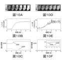
- FIGS. 10A to 10F are the results of photographing confocal fluorescence images of HeLa cells.
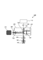
- FIG. 3 is a schematic diagram showing a configuration of a confocal microscope according to an embodiment of the present invention.
- the confocal microscope 100 includes a light source 110, a multimode optical fiber 120, a confocal scanner unit 130 of the present invention, a first imaging lens 140, an objective lens 150, A filter wheel 160 and a CCD camera 170 are included.
- the light source 110 emits excitation light to the multimode optical fiber 120.
- the type of the light source 110 is not particularly limited, and a white light source or the like can be used as well as a conventionally used laser light source.
- white light sources include LED light sources, mercury arc lamps, xenon arc lamps, and halogen lamps.
- the multimode optical fiber 120 propagates the excitation light emitted from the light source 110 to the confocal scanner unit 130.
- a multimode optical fiber is used instead of a single mode optical fiber in order to eliminate unevenness in the light intensity of the excitation light (see Non-Patent Document 2).
- the confocal scanner unit 130 includes a collimator lens 131, a microlens array disk 132, a dichroic mirror 133, a nipou disk 134, and a second imaging lens 135.
- the collimator lens 131 collimates the excitation light emitted from the multimode optical fiber 120.
- the collimator lens 131 is arranged such that the distance between the center of the emission end of the multimode optical fiber 120 and the center of the collimator lens is the focal length f of the collimator lens (see FIG. 6).
- the microlens array disk 132 is a circular substrate on which a plurality of microlenses are arranged.
- the plurality of microlenses are arranged in the same pattern as the pinhole of the Niipou disk 134.
- the microlens array disk 132 and the nipou disk 134 are connected by a connecting drum so as to be parallel to each other, and can rotate integrally around a rotation axis.
- the Nipou disk 134 is a circular light shielding substrate (pinhole array disk) having a plurality of pinholes.
- the Nipkow disk 134 has a pinhole at a position corresponding to the condensing point of the microlens of the microlens array disk 132.
- the kind of light shielding substrate is not particularly limited.
- the light shielding substrate is a glass substrate having a light shielding film formed on the surface thereof.
- the pinhole arrangement method is not particularly limited, but an equal pitch spiral arrangement is preferable from the viewpoint of preventing uneven illumination and uneven scan. When pinholes are arranged in an equi-pitch spiral arrangement, the center-to-center distance between adjacent pinholes is the same distance ("center-to-center distance D2" described later).
- the dichroic mirror 133 is disposed between the microlens array disk 132 and the nipou disk 134.
- the dichroic mirror 133 passes the excitation light incident from the microlens array disk 132 side to the Nipkow disk 134 side.
- the dichroic mirror 133 reflects fluorescence incident from the side of the Nipkow disk 134 to the second imaging lens 135 side.
- the second imaging lens 135 causes the CCD camera 170 to image the fluorescence reflected by the dichroic mirror 133.
- the first imaging lens 140 and the objective lens 150 constitute an infinite correction optical system.
- the first imaging lens 140 and the objective lens 150 collect the excitation light that has passed through the pinhole of the Niipou disc 134 on the focal plane of the sample 180.
- the first imaging lens 140 and the objective lens 150 collect the fluorescence emitted from the sample 180 in the pinhole of the nipou disk 134.
- the filter wheel 160 has various filters, and allows only the fluorescence having a specific wavelength among the fluorescence from the sample 180 to pass through.
- the CCD camera 170 detects the fluorescence that has passed through the filter of the filter wheel 160.
- the excitation light emitted from the light source 110 propagates through the multimode optical fiber 120 and is emitted from the emission end of the multimode optical fiber 120.
- the excitation light is collimated by the collimator lens 131 and irradiated to the microlens array disk 132.
- the excitation light is focused on the corresponding pinhole of the Niipou disk 134 by the action of each microlens of the microlens array disk 132.
- the excitation light that has passed through the pinhole passes through the first imaging lens 140 and the objective lens 150 and is focused on the focal plane of the sample 180.
- the sample 180 that has received the excitation light emits fluorescence.
- the fluorescence emitted from the sample 180 passes through the first imaging lens 140 and the objective lens 150 and returns to the confocal scanner unit 130.
- the fluorescent light again passes through the pinhole of the Nipkow disk 134 and is reflected by the dichroic mirror 133.
- the reflected fluorescence passes through the second imaging lens 135 and the filter wheel 160 and is detected by the CCD camera 170.
- the microlens array disk 132 and the Nipo disk 134 are rotated, a plurality of beams (excitation light) that have passed through the pinholes scan the focal plane of the sample 180 in parallel (multi-beam scan). Further, the fluorescence emitted from the sample 180 scans the imaging surface of the CCD camera 170 after passing through the same pinhole. Thereby, the fluorescence of the focal plane of the sample 180 is detected by the CCD camera 170. Light other than the focal plane cannot pass through the pinhole and therefore cannot reach the CCD camera 170. Therefore, the CCD camera 170 can capture a confocal image consisting only of the fluorescence on the focal plane of the sample 180.
- the focal length of the collimator lens 131 is f (mm)
- the core radius of the multimode optical fiber 120 is y 1 (mm)
- the microlens array disk 132 and the Niipou disk 134 When the center distance is D1 (mm) and the center distance between pinholes in the Niipou disc 134 is D2 (mm), the following expression (1) is satisfied.
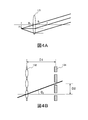
- y 1 (mm) / f (mm) on the left side means the diffusion angle ⁇ 1 (rad) of the excitation light collimated by the collimator lens 131.
- the diffusion angle ⁇ 1 is y 1 / f (rad).
- “D2 (mm) / D1 (mm)” on the right side means the angle ⁇ 2 (rad) shown in FIG. 4B.
- the angle ⁇ 2 (rad) is a pin adjacent to the pinhole corresponding to the center of the microlens and the line (optical axis) connecting the center of the microlens and the center of the corresponding pinhole. The angle of the line connecting the center of the hole.
- ⁇ 1 is the diffusion angle ⁇ 1 (rad) of the collimated excitation light.
- ⁇ 2 is an angle for the excitation light that has passed through the microlens to pass through a pinhole adjacent to the corresponding pinhole.
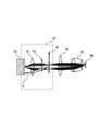
- FIG. 5 is a schematic diagram showing the configuration of the optical system of the conventional confocal microscope 10 'shown in FIG.
- the light when pump light is introduced into a conventional confocal scanner unit 40 using a multimode optical fiber 30 ′, the light is emitted from the end (near the outer periphery) of the core of the multimode optical fiber 30 ′. Since the light A passes through the collimator lens 41 and proceeds obliquely with respect to the optical axis, it cannot pass through the pinhole of the Niipou disc 45. That is, the light A emitted from the end of the core cannot be used as excitation light.
- the optical system of the conventional confocal scanner unit 40 is designed for a laser that is an ideal point light source.
- a lens having a long focal length (for example, 100 mm) and a small numerical aperture (for example, 0.1 or less) is used as the collimator lens 41.
- a collimator lens having a long focal length is used, it is difficult to satisfy the above formula (1).
- the present inventor thought that the pumping efficiency could be increased if the light emitted from the end of the core of the multimode optical fiber could also be used as the pumping light. Therefore, as a result of intensive studies, the present inventors have found that if the optical system is constructed so as to satisfy the above formula (1), the light emitted from the end of the core of the multimode optical fiber can also be used as the excitation light. It was.
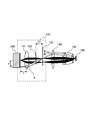
- FIG. 6 is a schematic diagram showing the configuration of the optical system of the confocal microscope 100 of the present invention shown in FIG.
- the optical system is constructed so as to satisfy the above formula (1) (for example, if a collimator lens 131 with a short focal length is selected), from the end of the core of the multimode optical fiber 120.
- the emitted light A can also pass through the pinhole of the Nipkow disk 134 after passing through the collimator lens 131.
- the light A emitted from the end portion of the core passes through the microlens and then obliquely passes through the pinhole adjacent to the pinhole corresponding to the microlens.
- the light that has passed through the pinhole obliquely is focused on the focal plane of the sample 180 in the same manner as the light that has passed straight through the pinhole. Therefore, the light A emitted from the end portion of the core can also contribute as excitation light.
- the confocal scanner unit of the present invention can also use the light emitted from the end of the core of the multimode optical fiber as the excitation light, so that the excitation efficiency is higher than that of the conventional confocal scanner unit. Are better.
- the confocal scanner unit of the present invention is applied to the confocal microscope.
- the application of the confocal scanner unit of the present invention is not limited to the confocal microscope.
- the confocal scanner unit of the present invention can be applied to a confocal endoscope, an optical coherence tomography (OCT) apparatus, and the like.
- This example shows the results of evaluating the performance of a confocal microscope having the confocal scanner unit of the present invention.
- optical system White light source multi-mode optical fiber (APCH1000; core diameter 1 mm, numerical aperture 0.39, length 2 m; Fiberguide industries Inc.), collimator lens, confocal scanner unit (CSU10; Yokogawa Electric Corporation) ), An electric inverted microscope (Eclipse Ti-E; Nikon Corporation), a filter wheel (Ludl Electronic Products Ltd.) and an EM-CCD camera (ImagEM; Hamamatsu Photonics Corporation) were used to construct an optical system.
- APCH1000 core diameter 1 mm, numerical aperture 0.39, length 2 m; Fiberguide industries Inc.
- collimator lens CSU10; Yokogawa Electric Corporation
- An electric inverted microscope Eclipse Ti-E; Nikon Corporation
- a filter wheel Lidl Electronic Products Ltd.
- EM-CCD camera ImagEM; Hamamatsu Photonics Corporation
- FIG. 7 is a schematic diagram showing the configuration of the constructed optical system.
- reference numeral 110 denotes a light source (white light source)
- reference numeral 120 denotes a multimode optical fiber
- reference numeral 131 denotes a collimator lens
- reference numeral 40 denotes a commercially available confocal scanner unit (see FIG. 1)
- reference numeral 140 denotes a first imaging.
- Reference numeral 150 denotes an objective lens
- reference numeral 160 denotes a filter wheel
- reference numeral 170 denotes a CCD camera
- reference numeral 180 denotes a sample.
- a lens having a magnification of 4 to 20 times (focal length of 10 to 50 mm).
- the excitation light that has passed through the collimator lens 131 installed separately after removing the mirror 42 of the confocal scanner unit 40 is applied to the microlens array disk 43 of the confocal scanner unit 40.
- the optical system was adjusted to irradiate. Whichever lens is used, the exit end of the multimode optical fiber 120 is placed at the focal position of the collimator lens 131 (or the collimator lens 41).
- the collimator lens 131 is a lens with a magnification of 4 times (Plan Apo 4x; focal length 50 mm, numerical aperture 0.20; Nikon Corporation), and a lens with a magnification of 10 times (Plan Apo 10x; focal length 20 mm, numerical aperture 0.45; Nikon Corporation) or a lens with a magnification of 20 times (Plan-Fluor 20x; focal length 10 mm, numerical aperture 0.50; Nikon Corporation) was used.
- As the objective lens 150 of the microscope an oil immersion lens (Plan Fluor 40x; numerical aperture 1.30; Nikon Corporation) having a magnification of 40 times was used.
- a multimode optical fiber having a core diameter of 1 mm is used. Therefore, when a lens with a magnification of 4 times (focal length 50 mm) is used, the diffusion angle ⁇ 1 is 0.010 rad. Similarly, when using 10X magnification of the lens (focal length 20 mm), the diffusion angle theta 1 is 0.025rad, and when using a magnification 20x of the lens (focal length 10 mm), the diffusion angle theta 1 0. 050 rad. Further, when the collimator lens 41 (focal length of 100 mm or more) included in the confocal scanner unit 40 is used, the diffusion angle ⁇ 1 is 0.005 rad or less.
- the center distance D1 between the microlens array disk 43 and the tip disk 45 included in the confocal scanner unit 40 is 10 mm.
- the intensity of excitation light at the tip of the objective lens 150 was measured.
- a white light source (SPECTRA7 Light Engine; Lumencor, Inc.) was used as the light source.
- Excitation light having a wavelength of 475/28 nm (transmission center wavelength / half width) from the light source 110 was introduced into the multimode optical fiber 120.
- the excitation light propagated through the multimode optical fiber 120 is applied to a collimator lens 131 having a magnification of 4 to 20 times (focal length 10 to 50 mm) or a fiber port for laser of a confocal scanner unit (indicated by “B” in FIG. 7). Introduced.
- the intensity of the excitation light was measured using an optical power meter (3664; Hioki Electric Co., Ltd.).
- FIG. 8 is a graph showing measurement results of the intensity of excitation light.
- the magnification is 10 times (focal length 20 mm) or 20 times magnification (focal length 10 mm), compared to the case where excitation light is introduced into the laser fiber port (collimator lens focal length 100 mm or more).
- the intensity of the excitation light was remarkably improved to 3.7 times and 3.6 times, respectively.
- a collimator lens having a magnification of 4 times was used, the intensity of the excitation light was hardly improved (1.3 times). From this result, it is understood that the intensity of the excitation light is remarkably increased by using a collimator lens satisfying ⁇ 1 ⁇ ⁇ 2 .
- the fluorescence intensity from the fluorescent beads was measured.
- the sample used was a 0.2 ⁇ m diameter fluorescent bead (Tetraspeck; Invitrogen Corporation).
- the excitation light is 475/28 nm light from a white light source (SPECTRA7 Light Engine; Lumencor, Inc.), 470/40 nm light from a 100 W mercury arc lamp (OSRAM GmbH), or an argon ion laser (Sapphire 488 LP). Light with a wavelength of 488 nm from Coherent, Inc) was used.
- Light having a wavelength of 475/28 nm from a white light source was introduced into a collimator lens (focal length 20 mm) having a magnification of 10 times.
- a collimator lens having a magnification of 10 times.
- light with a wavelength of 470/40 nm from a mercury arc lamp or a wavelength of 488 nm from an argon ion laser was introduced into the laser fiber port of the confocal scanner unit (focal length of collimator lens of 100 mm or more).
- the distribution of fluorescence intensity from the fluorescent beads irradiated with excitation light under each condition was measured, and the average value of 10 beads was obtained.
- FIG. 9 is a graph showing the distribution of fluorescence intensity under each condition.
- the full width at half maximum in the x-axis direction was 0.31 ⁇ m
- the full width at half maximum in the y-axis direction was 0.31 ⁇ m
- the full width at half maximum in the z-axis direction was 0.63 ⁇ m.
- the full width at half maximum in the x axis direction was 0.32 ⁇ m
- the full width at half maximum in the y axis direction was 0.33 ⁇ m
- the full width at half maximum in the z axis direction was 0.84 ⁇ m.
- the full width at half maximum in the x-axis direction was 0.28 ⁇ m
- the full width at half maximum in the y-axis direction was 0.29 ⁇ m
- the full width at half maximum in the z-axis direction was 0.61 ⁇ m.
- the confocal microscope of the present invention has a spatial resolution comparable to that of the conventional confocal microscope.
- FIG. 10A is a ratio image (YFP / CFP; 1-3 seconds after histamine stimulation) taken using the confocal microscope of the present invention.
- FIG. 10D is a ratio image (YFP / CFP; 1-3 seconds after histamine stimulation) taken using a conventional confocal microscope.
- 10A and 10D are images taken of the same cell. The ratio image was created by dividing the YFP fluorescence intensity by the CFP fluorescence intensity for each pixel using the acquired YFP image (535 nm) and CFP image (480 nm).
- FIG. 10B is a graph showing the change over time of the average ratio value in the region of interest (region surrounded by a square) shown in FIG. 10A.
- FIG. 10E is a graph showing the change over time of the average ratio value in the region of interest shown in FIG. 10D.
- FIG. 10C is a graph showing the change over time in the average fluorescence intensity of YFP and CFP in the region of interest shown in FIG. 10A.
- FIG. 10F is a graph showing the time-dependent change in the average fluorescence intensity of YFP and CFP in the region of interest shown in FIG. 10D.
- the interpolated view of FIG. 10F is a graph in which the vertical axis of the graph of FIG. 10F is enlarged.
- the confocal scanner unit of the present invention can be applied to, for example, a confocal microscope, a confocal endoscope, and an optical coherence tomography apparatus.
Landscapes
- Physics & Mathematics (AREA)
- Chemical & Material Sciences (AREA)
- Analytical Chemistry (AREA)
- General Physics & Mathematics (AREA)
- Optics & Photonics (AREA)
- Microscoopes, Condenser (AREA)
Abstract
共焦点スキャナユニットは、マルチモード光ファイバから出射された光をコリメートするコリメータレンズと、コリメート光を集光する複数のマイクロレンズを有するマイクロレンズアレイディスクと、マイクロレンズアレイディスクに対して平行に配置され、かつ複数のマイクロレンズの集光点に対応する位置に複数のピンホールを有するニポウディスクとを有する。コリメータレンズの焦点距離をf(mm)とし、マルチモード光ファイバのコアの半径をy1(mm)とし、マイクロレンズアレイディスクとニポウディスクとの中心間距離をD1(mm)とし、ニポウディスクにおけるピンホール間の中心間距離をD2(mm)としたときに、以下の式(1)が満たされる。
Description
本発明は、マイクロレンズアレイディスクおよびニポウディスクを用いたマルチビーム方式の共焦点スキャナユニット、ならびに前記共焦点スキャナユニットを有する共焦点顕微鏡に関する。
蛍光顕微鏡は、生体内のタンパク質や分子などを観察するための必要不可欠のツールとして、生命科学分野の研究で使用されてきた。特に、共焦点(蛍光)顕微鏡は、厚みのある生体サンプルについて一連の断層像を得ることができるため、生体機能の解明に必須のツールとなっている。従来の共焦点顕微鏡では、光源としてレーザを使用していた(共焦点レーザ顕微鏡)。
共焦点顕微鏡では、励起光の焦点をスキャンする必要がある。共焦点顕微鏡のスキャン方式は、ガルバノミラー方式とニポウ(Nipkow)ディスク方式とに大別される。ガルバノミラー方式では、試料中の1点にビームを集光して、このビームをラスタースキャンする(シングルビームスキャン)。この方式では、1枚の共焦点画像(1000×1000ピクセル)を得るのに1秒程度の時間がかかってしまう。一方、ニポウディスク方式では、ニポウディスクと称される、複数のピンホールが形成された円板を使用する。ニポウディスク方式では、回転しているニポウディスクに励起光を面照射して、多数(例えば、1000本)のビームを生成する。そして、生成された多数のビームで、並行して試料をスキャンする(マルチビームスキャン)。この方式では、例えば1/2000秒で1枚の共焦点画像(1000×1000ピクセル)を得ることができる。
ニポウディスク方式の共焦点顕微鏡において、ニポウディスクに励起光を直接照射すると、ピンホールを通過できる励起光の割合は1%程度となってしまい、明るい共焦点画像を得ることができない。この問題を解決するため、マイクロレンズアレイディスクとニポウディスクとを組み合わせて使用する共焦点スキャナユニットが開発されている。
図1は、従来の共焦点顕微鏡の構成を示す模式図である。図1に示されるように、従来の共焦点顕微鏡10は、レーザ光源20、シングルモード光ファイバ30、従来の共焦点スキャナユニット40、第1の結像レンズ50、対物レンズ60およびCCDカメラ70を有する。共焦点スキャナユニット40は、コリメータレンズ41、ミラー42、マイクロレンズアレイディスク43、ダイクロイックミラー44、ニポウディスク45および第2の結像レンズ46を有する。
図1に示されるように、従来の共焦点顕微鏡10では、レーザ光源20から出射された励起光は、シングルモード光ファイバ30内を伝播し、コリメータレンズ41によりコリメートされる。コリメートされた励起光は、マイクロレンズアレイディスク43のマイクロレンズにより集光され、ニポウディスク45のピンホールを通過する。ピンホールを通過した励起光は、第1の結像レンズ50および対物レンズ60を通過して試料80の焦点面に照射される。試料80から放出された蛍光は、再度ニポウディスク45のピンホールを通過して、ダイクロイックミラー44で反射される。反射した蛍光は、第2の結像レンズ46を通過して、CCDカメラ70により検出される。
図1に示されるような従来の共焦点顕微鏡では、光源としてレーザを使用するため、選択できる励起光の波長が限られている。このため、従来の共焦点顕微鏡には、使用するレーザの波長に合わせて蛍光プローブを選択しなければならないという問題がある。また、従来の共焦点顕微鏡には、光源としてレーザを使用するため、セットアップやメンテナンスに要する時間、労力および金銭での負担が非常に大きいという問題もある。これらの問題を解決するために、光源として白色光源(例えば、水銀アークランプやハロゲンランプなど)を使用することが提案されている(例えば、非特許文献1,2参照)。
たとえば、非特許文献1には、光源としてレーザおよび白色光源(水銀アークランプまたはハロゲンランプ)の両方を備えた共焦点顕微鏡が記載されている。非特許文献1に記載の共焦点顕微鏡では、光源としてレーザを使用する場合には、ニポウディスクを使用して励起光を試料に照射する(共焦点観察)。一方で、光源として水銀アークランプまたはハロゲンランプする場合には、蛍光画像が暗くなることを回避するために、ニポウディスクを使用しないで励起光を試料に照射している(非共焦点観察)。したがって、非特許文献1に記載の共焦点顕微鏡では、白色光源を使用する場合は、ニポウディスクを使用した高速観察を行うことができない。
非特許文献2には、光源として水銀アークランプを使用した共焦点顕微鏡が記載されている。図2は、非特許文献2に記載されている従来の共焦点顕微鏡の構成を示す模式図である。図2に示されるように、非特許文献2に記載の共焦点顕微鏡10’は、レーザ光源20(図1参照)の代わりに白色光源20’(水銀アークランプ)を有する。また、共焦点顕微鏡10’は、白色光の光強度のムラを解消するために、シングルモード光ファイバ30(図1参照)の代わりにマルチモード光ファイバ30’を有する。さらに、共焦点顕微鏡10’は、特定波長の蛍光のみを検出するためにフィルタホイール90を有する。非特許文献2に記載の共焦点顕微鏡では、光源として水銀アークランプを使用する場合も、ニポウディスクを使用して励起光を試料に照射する(共焦点観察)。
非特許文献2に記載の共焦点顕微鏡を使用することで、使用できる蛍光プローブの種類が制限されることなく、高速で蛍光観察を行うことができる。しかしながら、非特許文献2に記載の共焦点顕微鏡では、励起効率が低くなってしまい、高速観察において十分なシグナルが得られないことがある(後述)。
蛭川英男,外3名,「機能向上を実現した共焦点スキャナCSU-X1を支える新技術(New technologies for CSU-X1 confocal scanner unit)」,横河技報(Yokogawa technical report),Vol.52,No.1,pp.13-18.
Saito K, et al., "A mercury arc lamp-based multi-color confocal real time imaging system for cellular structure and function", Cell Struct. Funct., Vol.33, No.1, pp.133-141.
以上のように、ニポウディスク方式の共焦点スキャナユニットにおいて、光源として白色光源を使用する場合、試料に光を十分に照射することができず、高速観察において十分なシグナルが得られないという問題がある。
本発明の目的は、光源として白色光源を使用する場合であっても、高速観察において十分なシグナルを得られるニポウディスク方式の共焦点スキャナユニット、および前記共焦点スキャナユニットを有する共焦点顕微鏡を提供することである。
本発明者は、マルチモード光ファイバのコアの半径、コリメータレンズの焦点距離、マイクロレンズアレイディスクとニポウディスクとの中心間距離、およびニポウディスクにおけるピンホール間の中心間距離が所定の条件を満たすようにコリメータレンズを選択することで、上記課題を解決できることを見出し、さらに検討を加えて本発明を完成させた。
すなわち、本発明は、以下の共焦点スキャナユニットに関する。
[1]マルチモード光ファイバから出射された光をコリメートするコリメータレンズと;前記コリメータレンズによりコリメートされた光を集光する複数のマイクロレンズを有するマイクロレンズアレイディスクと;前記マイクロレンズアレイディスクに対して平行に配置され、かつ前記複数のマイクロレンズの集光点に対応する位置に複数のピンホールを有するニポウディスクとを有し;前記コリメータレンズは、前記マルチモード光ファイバの出射端の中心部と前記コリメータレンズの中心部との距離が前記コリメータレンズの焦点距離fとなるように配置されており;前記コリメータレンズの焦点距離をf(mm)とし、前記マルチモード光ファイバのコアの半径をy1(mm)とし、前記マイクロレンズアレイディスクと前記ニポウディスクとの中心間距離をD1(mm)とし、前記ニポウディスクにおける前記ピンホール間の中心間距離をD2(mm)としたときに、以下の式(1)が満たされる、共焦点スキャナユニット。

[1]マルチモード光ファイバから出射された光をコリメートするコリメータレンズと;前記コリメータレンズによりコリメートされた光を集光する複数のマイクロレンズを有するマイクロレンズアレイディスクと;前記マイクロレンズアレイディスクに対して平行に配置され、かつ前記複数のマイクロレンズの集光点に対応する位置に複数のピンホールを有するニポウディスクとを有し;前記コリメータレンズは、前記マルチモード光ファイバの出射端の中心部と前記コリメータレンズの中心部との距離が前記コリメータレンズの焦点距離fとなるように配置されており;前記コリメータレンズの焦点距離をf(mm)とし、前記マルチモード光ファイバのコアの半径をy1(mm)とし、前記マイクロレンズアレイディスクと前記ニポウディスクとの中心間距離をD1(mm)とし、前記ニポウディスクにおける前記ピンホール間の中心間距離をD2(mm)としたときに、以下の式(1)が満たされる、共焦点スキャナユニット。
また、本発明は、以下の共焦点顕微鏡に関する。
[2][1]に記載の共焦点スキャナユニットと;励起光を出射する光源と;前記励起光を前記共焦点スキャナユニットに伝播するマルチモード光ファイバとを有する、共焦点顕微鏡。
[3]前記光源は、白色光源である、[2]に記載の共焦点顕微鏡。
[4]前記光源は、LED光源、水銀アークランプ、キセノンアークランプまたはハロゲンランプである、[3]に記載の共焦点顕微鏡。
[2][1]に記載の共焦点スキャナユニットと;励起光を出射する光源と;前記励起光を前記共焦点スキャナユニットに伝播するマルチモード光ファイバとを有する、共焦点顕微鏡。
[3]前記光源は、白色光源である、[2]に記載の共焦点顕微鏡。
[4]前記光源は、LED光源、水銀アークランプ、キセノンアークランプまたはハロゲンランプである、[3]に記載の共焦点顕微鏡。
本発明の共焦点スキャナユニットは、光源として白色光源を使用する場合であっても、高速観察において十分なシグナルを得ることができる。
以下、本発明の実施の形態について、図面を参照して詳細に説明する。以下の説明では、本発明の共焦点スキャナユニットを有する共焦点顕微鏡について説明する。
図3は、本発明の一実施の形態に係る共焦点顕微鏡の構成を示す模式図である。図3に示されるように、本実施の形態に係る共焦点顕微鏡100は、光源110、マルチモード光ファイバ120、本発明の共焦点スキャナユニット130、第1の結像レンズ140、対物レンズ150、フィルタホイール160およびCCDカメラ170を有する。
光源110は、励起光をマルチモード光ファイバ120に出射する。光源110の種類は、特に限定されず、従来から使用されているレーザ光源だけでなく、白色光源などを使用することもできる。白色光源の例には、LED光源、水銀アークランプ、キセノンアークランプ、ハロゲンランプが含まれる。
マルチモード光ファイバ120は、光源110から出射された励起光を共焦点スキャナユニット130に伝播する。本発明の共焦点顕微鏡では、励起光の光強度のムラを解消するために、シングルモード光ファイバではなくマルチモード光ファイバを使用する(非特許文献2参照)。
共焦点スキャナユニット130は、コリメータレンズ131、マイクロレンズアレイディスク132、ダイクロイックミラー133、ニポウディスク134および第2の結像レンズ135を有する。
コリメータレンズ131は、マルチモード光ファイバ120から出射された励起光をコリメートする。コリメータレンズ131は、マルチモード光ファイバ120の出射端の中心部とコリメータレンズの中心部との距離がコリメータレンズの焦点距離fとなるように配置されている(図6参照)。
マイクロレンズアレイディスク132は、複数のマイクロレンズが配置された円形状の基板である。複数のマイクロレンズは、ニポウディスク134のピンホールと同じパターンで配置されている。マイクロレンズアレイディスク132およびニポウディスク134は、互いに平行になるように連結ドラムで連結されており、回転軸を中心として一体となって回転することができる。
ニポウディスク134は、複数のピンホールを有する円形状の遮光基板(ピンホールアレイディスク)である。ニポウディスク134は、マイクロレンズアレイディスク132のマイクロレンズの集光点に対応する位置にピンホールを有する。遮光基板の種類は、特に限定されない。たとえば、遮光基板は、その表面に遮光膜を形成されたガラス基板である。ピンホールの配置方式は、特に限定されないが、照度むらおよびスキャンむらを防ぐ観点から等ピッチ螺旋配置が好ましい。等ピッチ螺旋配置でピンホールを配置した場合、互いに隣接するピンホール間の中心間距離が、同一距離となる(後述する「中心間距離D2」)。
ダイクロイックミラー133は、マイクロレンズアレイディスク132とニポウディスク134との間に配置されている。ダイクロイックミラー133は、マイクロレンズアレイディスク132側から入射する励起光をニポウディスク134側に通過させる。一方、ダイクロイックミラー133は、ニポウディスク134側から入射する蛍光を第2の結像レンズ135側に反射させる。
第2の結像レンズ135は、ダイクロイックミラー133で反射された蛍光をCCDカメラ170に結像させる。
第1の結像レンズ140および対物レンズ150は、無限補正光学系を構成する。第1の結像レンズ140および対物レンズ150は、ニポウディスク134のピンホールを通過した励起光を試料180の焦点面に集光させる。また、第1の結像レンズ140および対物レンズ150は、試料180から放出された蛍光をニポウディスク134のピンホールに集光させる。
フィルタホイール160は、各種フィルタを有しており、試料180からの蛍光のうち、特定波長の蛍光のみを通過させる。
CCDカメラ170は、フィルタホイール160のフィルタを通過してきた蛍光を検出する。
次に、図3を参照して、共焦点顕微鏡100の動作について説明する。
光源110から出射された励起光は、マルチモード光ファイバ120内を伝播し、マルチモード光ファイバ120の出射端から出射される。共焦点スキャナユニット130内において、励起光は、コリメータレンズ131によりコリメートされ、マイクロレンズアレイディスク132に照射される。励起光は、マイクロレンズアレイディスク132の各マイクロレンズの作用により、ニポウディスク134の対応するピンホールにおいて焦点を結ぶ。ピンホールを通過した励起光は、第1の結像レンズ140および対物レンズ150を通過して試料180の焦点面に焦点を結ぶ。
励起光を受けた試料180は、蛍光を放出する。試料180から放出された蛍光は、第1の結像レンズ140および対物レンズ150を通過して共焦点スキャナユニット130内に戻る。蛍光は、再度ニポウディスク134のピンホールを通過して、ダイクロイックミラー133で反射される。反射した蛍光は、第2の結像レンズ135およびフィルタホイール160を通過して、CCDカメラ170により検出される。
ここで、マイクロレンズアレイディスク132およびニポウディスク134を回転させると、ピンホールを通過した複数のビーム(励起光)が、試料180の焦点面を並行してスキャンする(マルチビームスキャン)。また、試料180から放出された蛍光は、同じピンホールを通過した後に、CCDカメラ170の撮像面をスキャンする。これにより、試料180の焦点面の蛍光が、CCDカメラ170により検出される。焦点面以外の光は、ピンホールをほとんど通過できないため、CCDカメラ170に到達することができない。したがって、CCDカメラ170は、試料180の焦点面の蛍光のみからなる共焦点画像を撮影することができる。
本発明の共焦点スキャナユニット130は、コリメータレンズ131の焦点距離をf(mm)とし、マルチモード光ファイバ120のコアの半径をy1(mm)とし、マイクロレンズアレイディスク132とニポウディスク134との中心間距離をD1(mm)とし、ニポウディスク134におけるピンホール間の中心間距離をD2(mm)としたときに、以下の式(1)が満たされることを特徴とする。

上記式(1)において、左辺の「y1(mm)/f(mm)」は、コリメータレンズ131によりコリメートされた励起光の拡散角θ1(rad)を意味する。図4Aに示されるように、コリメータレンズ131の焦点面に半径y1(mm)の光源を置いた場合、拡散角θ1はy1/f(rad)となる。
一方、上記式(1)において、右辺の「D2(mm)/D1(mm)」は、図4Bに示される角度θ2(rad)を意味する。図4Bに示されるように、角度θ2(rad)は、マイクロレンズの中心と対応するピンホールの中心とを結ぶ線(光軸)に対する、マイクロレンズの中心と対応するピンホールに隣接するピンホールの中心とを結ぶ線の角度である。
したがって、上記式(1)は、以下の式(2)と同じ意味である。前述の通り、θ1は、コリメートされた励起光の拡散角θ1(rad)である。また、θ2は、マイクロレンズを通過した励起光が、対応するピンホールに隣接するピンホールを通過するための角度である。

図5は、図2に示される従来の共焦点顕微鏡10’の光学系の構成を示す模式図である。図5に示されるように、従来の共焦点スキャナユニット40にマルチモード光ファイバ30’を用いて励起光を導入した場合、マルチモード光ファイバ30’のコアの端部(外周近傍)から出射された光Aは、コリメータレンズ41を通過した後、光軸に対して斜めに進むため、ニポウディスク45のピンホールを通過することができない。すなわち、コアの端部から出射された光Aは、励起光として利用できない。これは、従来の共焦点スキャナユニット40の光学系が、理想的な点光源であるレーザ用に設計されているためである。従来の共焦点スキャナユニット40では、コリメータレンズ41として、焦点距離が長く(例えば、100mm)、開口数の小さい(例えば、0.1以下)レンズを使用していた。このように焦点距離が長いコリメータレンズを使用した場合、上記式(1)を満たすことは困難である。
本発明者は、このマルチモード光ファイバのコアの端部から出射された光も励起光として利用することができれば、励起効率を高めることができるのではないかと考えた。そこで、本発明者は、鋭意検討した結果、上記式(1)を満たすように光学系を構築すれば、マルチモード光ファイバのコアの端部から出射された光も励起光として利用できることを見出したのである。
図6は、図3に示される本発明の共焦点顕微鏡100の光学系の構成を示す模式図である。図6に示されるように、上記式(1)を満たすように光学系を構築すれば(例えば、焦点距離の短いコリメータレンズ131を選択すれば)、マルチモード光ファイバ120のコアの端部から出射された光Aも、コリメータレンズ131を通過した後、ニポウディスク134のピンホールを通過することができる。このとき、コアの端部から出射された光Aは、マイクロレンズを通過した後、当該マイクロレンズに対応するピンホールに隣接するピンホールを斜めに通過する。ピンホールを斜めに通過した光は、ピンホールを真っ直ぐに通過した光と同様に、試料180の焦点面に焦点を結ぶ。したがって、コアの端部から出射された光Aも、励起光として寄与することができる。
以上のように、本発明の共焦点スキャナユニットは、マルチモード光ファイバのコアの端部から出射された光も励起光として利用することができるため、従来の共焦点スキャナユニットよりも励起効率に優れている。
なお、上記の説明では、本発明の共焦点スキャナユニットを共焦点顕微鏡に適用する例について説明したが、本発明の共焦点スキャナユニットの用途は共焦点顕微鏡に限定されるものではない。たとえば、本発明の共焦点スキャナユニットは、共焦点内視鏡や光干渉断層撮影(optical coherence tomography;OCT)装置などに適用することができる。
以下、本発明について実施例を参照して詳細に説明するが、本発明はこれらの実施例により限定されない。
本実施例では、本発明の共焦点スキャナユニットを有する共焦点顕微鏡の性能を評価した結果を示す。
1.光学系の構築
白色光源、マルチモード光ファイバ(APCH1000;コアの直径1mm、開口数0.39、長さ2m;Fiberguide industries Inc.)、コリメータレンズ、共焦点スキャナユニット(CSU10;横河電機株式会社)、電動倒立顕微鏡(エクリプスTi-E;株式会社ニコン)、フィルタホイール(Ludl Electronic Products Ltd.)およびEM-CCDカメラ(ImagEM;浜松ホトニクス株式会社)を用いて、光学系を構築した。
白色光源、マルチモード光ファイバ(APCH1000;コアの直径1mm、開口数0.39、長さ2m;Fiberguide industries Inc.)、コリメータレンズ、共焦点スキャナユニット(CSU10;横河電機株式会社)、電動倒立顕微鏡(エクリプスTi-E;株式会社ニコン)、フィルタホイール(Ludl Electronic Products Ltd.)およびEM-CCDカメラ(ImagEM;浜松ホトニクス株式会社)を用いて、光学系を構築した。
図7は、構築した光学系の構成を示す模式図である。図7において、符号110は光源(白色光源)、符号120はマルチモード光ファイバ、符号131はコリメータレンズ、符号40は市販の共焦点スキャナユニット(図1参照)、符号140は第1の結像レンズ、符号150は対物レンズ、符号160はフィルタホイール、符号170はCCDカメラ、符号180は試料を示す。
図7に示されるように、本実施例では、市販の共焦点スキャナユニット40に含まれるコリメータレンズ41(焦点距離100mm以上)の代わりに、倍率4~20倍(焦点距離10~50mm)のレンズをコリメータレンズ131として使用した。図1と図7とを比較するとわかるように、共焦点スキャナユニット40のミラー42を外して、別途設置されたコリメータレンズ131を通過した励起光が共焦点スキャナユニット40のマイクロレンズアレイディスク43に照射されるように、光学系を調整した。いずれのレンズを使用する場合であっても、マルチモード光ファイバ120の出射端は、コリメータレンズ131(またはコリメータレンズ41)の焦点位置に設置した。
コリメータレンズ131は、倍率4倍のレンズ(Plan Apo 4x;焦点距離50mm、開口数0.20;株式会社ニコン)、倍率10倍のレンズ(Plan Apo 10x;焦点距離20mm、開口数0.45;株式会社ニコン)または倍率20倍のレンズ(Plan Fluor 20x;焦点距離10mm、開口数0.50;株式会社ニコン)を使用した。また、顕微鏡の対物レンズ150は、倍率40倍の油浸レンズ(Plan Fluor 40x;開口数1.30;株式会社ニコン)を使用した。
前述の通り、本実施例ではコアの直径が1mmのマルチモード光ファイバを使用している。したがって、倍率4倍のレンズ(焦点距離50mm)を使用した場合、拡散角θ1は0.010radとなる。同様に、倍率10倍のレンズ(焦点距離20mm)を使用した場合、拡散角θ1は0.025radとなり、倍率20倍のレンズ(焦点距離10mm)を使用した場合、拡散角θ1は0.050radとなる。また、共焦点スキャナユニット40に含まれるコリメータレンズ41(焦点距離100mm以上)を使用した場合、拡散角θ1は0.005rad以下となる。
一方、共焦点スキャナユニット40に含まれるマイクロレンズアレイディスク43とニポウディスク45との中心間距離D1は、10mmである。また、ニポウディスク45の隣接するピンホールの中心間距離D2は、0.25mmである。したがって、図4Bに示される角度θ2(=D2/D1)は、0.025radとなる。
2.励起光の強度の評価
本発明の共焦点顕微鏡について励起光量を評価するために、対物レンズ150の先端における励起光の強度を測定した。光源は、白色光源(SPECTRA7 Light Engine;Lumencor, Inc.)を使用した。光源110からの波長475/28nm(透過中心波長/半値幅)の励起光をマルチモード光ファイバ120に導入した。マルチモード光ファイバ120を伝播した励起光を、倍率4~20倍(焦点距離10~50mm)のコリメータレンズ131、または共焦点スキャナユニットのレーザ用ファイバーポート(図7において「B」で示す)に導入した。励起光の強度は、光パワーメータ(3664;日置電機株式会社)を用いて測定した。
本発明の共焦点顕微鏡について励起光量を評価するために、対物レンズ150の先端における励起光の強度を測定した。光源は、白色光源(SPECTRA7 Light Engine;Lumencor, Inc.)を使用した。光源110からの波長475/28nm(透過中心波長/半値幅)の励起光をマルチモード光ファイバ120に導入した。マルチモード光ファイバ120を伝播した励起光を、倍率4~20倍(焦点距離10~50mm)のコリメータレンズ131、または共焦点スキャナユニットのレーザ用ファイバーポート(図7において「B」で示す)に導入した。励起光の強度は、光パワーメータ(3664;日置電機株式会社)を用いて測定した。
図8は、励起光の強度の測定結果を示すグラフである。図8に示されるように、レーザ用ファイバーポート(コリメータレンズの焦点距離100mm以上)に励起光を導入した場合に比べて、倍率10倍(焦点距離20mm)または倍率20倍(焦点距離10mm)のコリメータレンズを使用した場合、それぞれ励起光の強度が3.7倍、3.6倍と顕著に向上した。一方、倍率4倍(焦点距離50mm)のコリメータレンズを使用した場合は励起光の強度はほとんど向上しなかった(1.3倍)。この結果から、θ1≧θ2を満たすコリメータレンズを使用することで、励起光の強度が顕著に高くなることがわかる。
3.空間分解能の評価
本発明の共焦点顕微鏡について空間分解能を評価するために、蛍光ビーズからの蛍光強度を測定した。試料は、直径0.2μmの蛍光ビーズ(Tetraspeck;Invitrogen Corporation)を使用した。励起光は、白色光源(SPECTRA7 Light Engine;Lumencor, Inc.)からの波長475/28nmの光、100W水銀アークランプ(OSRAM GmbH)からの波長470/40nmの光、またはアルゴンイオンレーザ(Sapphire 488 LP;Coherent, Inc)からの波長488nmの光を使用した。白色光源からの波長475/28nmの光は、倍率10倍のコリメータレンズ(焦点距離20mm)に導入した。一方、水銀アークランプからの波長470/40nmの光、またはアルゴンイオンレーザからの波長488nmは、共焦点スキャナユニットのレーザ用ファイバーポート(コリメータレンズの焦点距離100mm以上)に導入した。
本発明の共焦点顕微鏡について空間分解能を評価するために、蛍光ビーズからの蛍光強度を測定した。試料は、直径0.2μmの蛍光ビーズ(Tetraspeck;Invitrogen Corporation)を使用した。励起光は、白色光源(SPECTRA7 Light Engine;Lumencor, Inc.)からの波長475/28nmの光、100W水銀アークランプ(OSRAM GmbH)からの波長470/40nmの光、またはアルゴンイオンレーザ(Sapphire 488 LP;Coherent, Inc)からの波長488nmの光を使用した。白色光源からの波長475/28nmの光は、倍率10倍のコリメータレンズ(焦点距離20mm)に導入した。一方、水銀アークランプからの波長470/40nmの光、またはアルゴンイオンレーザからの波長488nmは、共焦点スキャナユニットのレーザ用ファイバーポート(コリメータレンズの焦点距離100mm以上)に導入した。
各条件で励起光を照射した蛍光ビーズからの蛍光強度の分布(x軸、y軸およびz軸方向)を測定し、10個のビーズの平均値を求めた。
図9は、各条件における蛍光強度の分布を示すグラフである。白色光源からの光を照射した場合、x軸方向の半値全幅は0.31μm、y軸方向の半値全幅は0.31μm、z軸方向の半値全幅は0.63μmであった。また、水銀アークランプからの光を照射した場合、x軸方向の半値全幅は0.32μm、y軸方向の半値全幅は0.33μm、z軸方向の半値全幅は0.84μmであった。また、アルゴンイオンレーザからの光を照射した場合、x軸方向の半値全幅は0.28μm、y軸方向の半値全幅は0.29μm、z軸方向の半値全幅は0.61μmであった。
これらの結果から、本発明の共焦点顕微鏡は、従来の共焦点顕微鏡の空間分解能と同程度の空間分解能を有していることがわかる。
4.共焦点蛍光画像の撮影
本発明の共焦点顕微鏡(図7参照)および従来の共焦点顕微鏡(図2参照)を用いて、イエローカメレオン(CFPおよびYFPを有するCa2+プローブ)を発現させたHeLa細胞の共焦点蛍光画像をリアルタイムで撮影した。
本発明の共焦点顕微鏡(図7参照)および従来の共焦点顕微鏡(図2参照)を用いて、イエローカメレオン(CFPおよびYFPを有するCa2+プローブ)を発現させたHeLa細胞の共焦点蛍光画像をリアルタイムで撮影した。
本発明の共焦点顕微鏡では、白色光源(SPECTRA7 Light Engine)からの波長440nmの光をマルチモード光ファイバに導入し、倍率10倍のコリメータレンズ(焦点距離20mm)によりコリメートした(図7参照)。一方、従来の共焦点顕微鏡では、100W水銀アークランプからの波長440nmの光をマルチモード光ファイバを通して、共焦点スキャナユニットのレーザ用ファイバーポート(コリメータレンズの焦点距離100mm以上)に導入した(図2参照)。
図10Aは、本発明の共焦点顕微鏡を用いて撮影されたレシオ画像(YFP/CFP;ヒスタミン刺激後1~3秒)である。図10Dは、従来の共焦点顕微鏡を用いて撮影されたレシオ画像(YFP/CFP;ヒスタミン刺激後1~3秒)である。図10Aおよび図10Dは、同一の細胞について撮影した画像である。レシオ画像は、取得したYFP画像(535nm)およびCFP画像(480nm)を用いて、各ピクセルについてYFPの蛍光強度をCFPの蛍光強度で割ることにより作成した。
図10Bは、図10Aに示される興味領域(四角で囲まれた領域)における平均レシオ値の経時変化を示すグラフである。図10Eは、図10Dに示される興味領域における平均レシオ値の経時変化を示すグラフである。また、図10Cは、図10Aに示される興味領域におけるYFPおよびCFPの平均蛍光強度の経時変化を示すグラフである。図10Fは、図10Dに示される興味領域におけるYFPおよびCFPの平均蛍光強度の経時変化を示すグラフである。図10Fの内挿図は、図10Fのグラフの縦軸を拡大したグラフである。
従来の共焦点顕微鏡を用いた場合、図10D~Fに示されるように、励起光の強度が不十分なため、鮮明な画像を取得することができなかった。その結果、Ca2+の濃度変化を詳細に観察することはできなかった。一方、本発明の共焦点顕微鏡を用いた場合、図10A~Cに示されるように、十分な強度の励起光を照射することができたため、鮮明な画像を取得することができた。その結果、Ca2+の濃度変化を詳細に観察することができた。
本出願は、2011年6月1日出願の特願2011-123041に基づく優先権を主張する。当該出願明細書および図面に記載された内容は、すべて本願明細書に援用される。
本発明の共焦点スキャナユニットは、例えば、共焦点顕微鏡、共焦点内視鏡、光干渉断層撮影装置などに適用することができる。
10,10’ 共焦点顕微鏡
20 レーザ光源
20’ 白色光源
30 シングルモード光ファイバ
30’ マルチモード光ファイバ
40 共焦点スキャナユニット
41 コリメータレンズ
42 ミラー
43 マイクロレンズアレイディスク
44 ダイクロイックミラー
45 ニポウディスク
46 第2の結像レンズ
50 第1の結像レンズ
60 対物レンズ
70 CCDカメラ
80 試料
90 フィルタホイール
100 共焦点顕微鏡
110 光源
120 マルチモード光ファイバ
130 共焦点スキャナユニット
131 コリメータレンズ
132 マイクロレンズアレイディスク
133 ダイクロイックミラー
134 ニポウディスク
135 第2の結像レンズ
140 第1の結像レンズ
150 対物レンズ
160 フィルタホイール
170 CCDカメラ
180 試料
20 レーザ光源
20’ 白色光源
30 シングルモード光ファイバ
30’ マルチモード光ファイバ
40 共焦点スキャナユニット
41 コリメータレンズ
42 ミラー
43 マイクロレンズアレイディスク
44 ダイクロイックミラー
45 ニポウディスク
46 第2の結像レンズ
50 第1の結像レンズ
60 対物レンズ
70 CCDカメラ
80 試料
90 フィルタホイール
100 共焦点顕微鏡
110 光源
120 マルチモード光ファイバ
130 共焦点スキャナユニット
131 コリメータレンズ
132 マイクロレンズアレイディスク
133 ダイクロイックミラー
134 ニポウディスク
135 第2の結像レンズ
140 第1の結像レンズ
150 対物レンズ
160 フィルタホイール
170 CCDカメラ
180 試料
Claims (4)
- マルチモード光ファイバから出射された光をコリメートするコリメータレンズと、
前記コリメータレンズによりコリメートされた光を集光する複数のマイクロレンズを有するマイクロレンズアレイディスクと、
前記マイクロレンズアレイディスクに対して平行に配置され、かつ前記複数のマイクロレンズの集光点に対応する位置に複数のピンホールを有するニポウディスクと、を有し、
前記コリメータレンズは、前記マルチモード光ファイバの出射端の中心部と前記コリメータレンズの中心部との距離が前記コリメータレンズの焦点距離fとなるように配置されており、
前記コリメータレンズの焦点距離をf(mm)とし、前記マルチモード光ファイバのコアの半径をy1(mm)とし、前記マイクロレンズアレイディスクと前記ニポウディスクとの中心間距離をD1(mm)とし、前記ニポウディスクにおける前記ピンホール間の中心間距離をD2(mm)としたときに、以下の式(1)が満たされる、

- 請求項1に記載の共焦点スキャナユニットと、
励起光を出射する光源と、
前記励起光を前記共焦点スキャナユニットに伝播するマルチモード光ファイバと、
を有する、共焦点顕微鏡。 - 前記光源は、白色光源である、請求項2に記載の共焦点顕微鏡。
- 前記光源は、LED光源、水銀アークランプ、キセノンアークランプまたはハロゲンランプである、請求項3に記載の共焦点顕微鏡。
Priority Applications (1)
| Application Number | Priority Date | Filing Date | Title |
|---|---|---|---|
| JP2013517824A JP5943432B2 (ja) | 2011-06-01 | 2012-04-13 | 共焦点顕微鏡 |
Applications Claiming Priority (2)
| Application Number | Priority Date | Filing Date | Title |
|---|---|---|---|
| JP2011-123041 | 2011-06-01 | ||
| JP2011123041 | 2011-06-01 |
Publications (1)
| Publication Number | Publication Date |
|---|---|
| WO2012164811A1 true WO2012164811A1 (ja) | 2012-12-06 |
Family
ID=47258689
Family Applications (1)
| Application Number | Title | Priority Date | Filing Date |
|---|---|---|---|
| PCT/JP2012/002598 Ceased WO2012164811A1 (ja) | 2011-06-01 | 2012-04-13 | 共焦点スキャナユニットおよび共焦点顕微鏡 |
Country Status (3)
| Country | Link |
|---|---|
| JP (1) | JP5943432B2 (ja) |
| TW (1) | TWI534473B (ja) |
| WO (1) | WO2012164811A1 (ja) |
Families Citing this family (2)
| Publication number | Priority date | Publication date | Assignee | Title |
|---|---|---|---|---|
| TWI892331B (zh) * | 2023-11-28 | 2025-08-01 | 中央研究院 | 掃描裝置及iscat共軛焦顯微鏡系統及其觀察方法 |
| CN120053897A (zh) * | 2025-04-16 | 2025-05-30 | 青岛镭视光电科技有限公司 | 一种波长精准控制的装置和光动力治疗仪 |
Citations (3)
| Publication number | Priority date | Publication date | Assignee | Title |
|---|---|---|---|---|
| JP2000126116A (ja) * | 1998-10-28 | 2000-05-09 | Olympus Optical Co Ltd | 光診断システム |
| JP2005283659A (ja) * | 2004-03-26 | 2005-10-13 | Olympus Corp | 走査型共焦点顕微鏡 |
| JP2007121590A (ja) * | 2005-10-27 | 2007-05-17 | Yokogawa Electric Corp | 共焦点スキャナ |
-
2012
- 2012-04-13 WO PCT/JP2012/002598 patent/WO2012164811A1/ja not_active Ceased
- 2012-04-13 JP JP2013517824A patent/JP5943432B2/ja active Active
- 2012-04-17 TW TW101113664A patent/TWI534473B/zh not_active IP Right Cessation
Patent Citations (3)
| Publication number | Priority date | Publication date | Assignee | Title |
|---|---|---|---|---|
| JP2000126116A (ja) * | 1998-10-28 | 2000-05-09 | Olympus Optical Co Ltd | 光診断システム |
| JP2005283659A (ja) * | 2004-03-26 | 2005-10-13 | Olympus Corp | 走査型共焦点顕微鏡 |
| JP2007121590A (ja) * | 2005-10-27 | 2007-05-17 | Yokogawa Electric Corp | 共焦点スキャナ |
Also Published As
| Publication number | Publication date |
|---|---|
| TW201303355A (zh) | 2013-01-16 |
| TWI534473B (zh) | 2016-05-21 |
| JPWO2012164811A1 (ja) | 2014-07-31 |
| JP5943432B2 (ja) | 2016-07-05 |
Similar Documents
| Publication | Publication Date | Title |
|---|---|---|
| EP3087423B1 (en) | Multi-foci multiphoton imaging systems and methods | |
| JP4670031B2 (ja) | 試料内で励起および/または後方散乱を経た光ビームの光学的検出のための装置 | |
| DK2594981T3 (en) | Methods and apparatus for confocal imaging | |
| EP2510395B1 (en) | Imaging distal end of multimode fiber | |
| JP4952784B2 (ja) | 生体用蛍光測定装置及び蛍光測定用励起光照射装置 | |
| JP2012237647A (ja) | 多焦点共焦点ラマン分光顕微鏡 | |
| US8089691B2 (en) | Projection device for patterned illumination and microscopy | |
| US11237370B2 (en) | Multiple inclined beam line-scanning imaging apparatus, methods, and applications | |
| JP2010271569A (ja) | 走査型顕微鏡装置 | |
| CN101228428A (zh) | 荧光纳米显微方法 | |
| KR101603726B1 (ko) | 멀티모달 현미경 | |
| US20180252648A1 (en) | Observation device | |
| TW201213849A (en) | Image generation device | |
| US8633432B2 (en) | Reflective focusing and transmissive projection device | |
| Fritzky et al. | Advanced methods in fluorescence microscopy | |
| CN107209110B (zh) | 高吞吐量生化筛查 | |
| RU2510959C2 (ru) | Устройство для анализа люминесцирующих биологических микрочипов | |
| Ulrich et al. | Compact multiphoton/single photon laser scanning microscope for spectral imaging and fluorescence lifetime imaging | |
| CN105849615B (zh) | 用于渐逝照明和点状扫描照明的显微镜 | |
| JP5943432B2 (ja) | 共焦点顕微鏡 | |
| CN119768726A (zh) | 照明装置的改进或与照明装置有关的改进 | |
| JP2002543370A (ja) | 光学スキャナ用の画像形成システム | |
| US12282147B2 (en) | Method and system for enhanced photon microscopy | |
| Jiao et al. | Smartphone‐based optical sectioning (SOS) microscopy with a telecentric design for fluorescence imaging | |
| CN223926705U (zh) | 一种多模态荧光显微镜 |
Legal Events
| Date | Code | Title | Description |
|---|---|---|---|
| 121 | Ep: the epo has been informed by wipo that ep was designated in this application |
Ref document number: 12793006 Country of ref document: EP Kind code of ref document: A1 |
|
| ENP | Entry into the national phase |
Ref document number: 2013517824 Country of ref document: JP Kind code of ref document: A |
|
| NENP | Non-entry into the national phase |
Ref country code: DE |
|
| 122 | Ep: pct application non-entry in european phase |
Ref document number: 12793006 Country of ref document: EP Kind code of ref document: A1 |