WO2012162325A1 - Host materials for oleds - Google Patents

Host materials for oleds Download PDF

Info

Publication number
WO2012162325A1
WO2012162325A1 PCT/US2012/039015 US2012039015W WO2012162325A1 WO 2012162325 A1 WO2012162325 A1 WO 2012162325A1 US 2012039015 W US2012039015 W US 2012039015W WO 2012162325 A1 WO2012162325 A1 WO 2012162325A1
Authority
WO
WIPO (PCT)
Prior art keywords
group
compound
mmol
aryl
phenyl
Prior art date
Application number
PCT/US2012/039015
Other languages
French (fr)
Inventor
Lichang Zeng
Alexey B. Dyatkin
Gregg Kottas
Original Assignee
Universal Display Corporation
Priority date (The priority date is an assumption and is not a legal conclusion. Google has not performed a legal analysis and makes no representation as to the accuracy of the date listed.)
Filing date
Publication date
Application filed by Universal Display Corporation filed Critical Universal Display Corporation
Priority to DE112012002237.8T priority Critical patent/DE112012002237B4/en
Priority to CN201280025504.8A priority patent/CN103596963B/en
Priority to KR1020137031783A priority patent/KR101922269B1/en
Publication of WO2012162325A1 publication Critical patent/WO2012162325A1/en

Links

Classifications

    • CCHEMISTRY; METALLURGY
    • C07ORGANIC CHEMISTRY
    • C07FACYCLIC, CARBOCYCLIC OR HETEROCYCLIC COMPOUNDS CONTAINING ELEMENTS OTHER THAN CARBON, HYDROGEN, HALOGEN, OXYGEN, NITROGEN, SULFUR, SELENIUM OR TELLURIUM
    • C07F7/00Compounds containing elements of Groups 4 or 14 of the Periodic System
    • C07F7/02Silicon compounds
    • C07F7/08Compounds having one or more C—Si linkages
    • C07F7/0803Compounds with Si-C or Si-Si linkages
    • C07F7/0805Compounds with Si-C or Si-Si linkages comprising only Si, C or H atoms
    • CCHEMISTRY; METALLURGY
    • C07ORGANIC CHEMISTRY
    • C07FACYCLIC, CARBOCYCLIC OR HETEROCYCLIC COMPOUNDS CONTAINING ELEMENTS OTHER THAN CARBON, HYDROGEN, HALOGEN, OXYGEN, NITROGEN, SULFUR, SELENIUM OR TELLURIUM
    • C07F7/00Compounds containing elements of Groups 4 or 14 of the Periodic System
    • C07F7/02Silicon compounds
    • C07F7/08Compounds having one or more C—Si linkages
    • C07F7/0803Compounds with Si-C or Si-Si linkages
    • C07F7/081Compounds with Si-C or Si-Si linkages comprising at least one atom selected from the elements N, O, halogen, S, Se or Te
    • C07F7/0812Compounds with Si-C or Si-Si linkages comprising at least one atom selected from the elements N, O, halogen, S, Se or Te comprising a heterocyclic ring
    • CCHEMISTRY; METALLURGY
    • C07ORGANIC CHEMISTRY
    • C07FACYCLIC, CARBOCYCLIC OR HETEROCYCLIC COMPOUNDS CONTAINING ELEMENTS OTHER THAN CARBON, HYDROGEN, HALOGEN, OXYGEN, NITROGEN, SULFUR, SELENIUM OR TELLURIUM
    • C07F7/00Compounds containing elements of Groups 4 or 14 of the Periodic System
    • C07F7/30Germanium compounds
    • HELECTRICITY
    • H10SEMICONDUCTOR DEVICES; ELECTRIC SOLID-STATE DEVICES NOT OTHERWISE PROVIDED FOR
    • H10KORGANIC ELECTRIC SOLID-STATE DEVICES
    • H10K50/00Organic light-emitting devices
    • HELECTRICITY
    • H10SEMICONDUCTOR DEVICES; ELECTRIC SOLID-STATE DEVICES NOT OTHERWISE PROVIDED FOR
    • H10KORGANIC ELECTRIC SOLID-STATE DEVICES
    • H10K50/00Organic light-emitting devices
    • H10K50/10OLEDs or polymer light-emitting diodes [PLED]
    • H10K50/11OLEDs or polymer light-emitting diodes [PLED] characterised by the electroluminescent [EL] layers
    • HELECTRICITY
    • H10SEMICONDUCTOR DEVICES; ELECTRIC SOLID-STATE DEVICES NOT OTHERWISE PROVIDED FOR
    • H10KORGANIC ELECTRIC SOLID-STATE DEVICES
    • H10K85/00Organic materials used in the body or electrodes of devices covered by this subclass
    • H10K85/40Organosilicon compounds, e.g. TIPS pentacene
    • HELECTRICITY
    • H10SEMICONDUCTOR DEVICES; ELECTRIC SOLID-STATE DEVICES NOT OTHERWISE PROVIDED FOR
    • H10KORGANIC ELECTRIC SOLID-STATE DEVICES
    • H10K85/00Organic materials used in the body or electrodes of devices covered by this subclass
    • H10K85/60Organic compounds having low molecular weight
    • H10K85/649Aromatic compounds comprising a hetero atom
    • H10K85/657Polycyclic condensed heteroaromatic hydrocarbons
    • H10K85/6572Polycyclic condensed heteroaromatic hydrocarbons comprising only nitrogen in the heteroaromatic polycondensed ring system, e.g. phenanthroline or carbazole
    • HELECTRICITY
    • H10SEMICONDUCTOR DEVICES; ELECTRIC SOLID-STATE DEVICES NOT OTHERWISE PROVIDED FOR
    • H10KORGANIC ELECTRIC SOLID-STATE DEVICES
    • H10K85/00Organic materials used in the body or electrodes of devices covered by this subclass
    • H10K85/60Organic compounds having low molecular weight
    • H10K85/649Aromatic compounds comprising a hetero atom
    • H10K85/657Polycyclic condensed heteroaromatic hydrocarbons
    • H10K85/6574Polycyclic condensed heteroaromatic hydrocarbons comprising only oxygen in the heteroaromatic polycondensed ring system, e.g. cumarine dyes
    • HELECTRICITY
    • H10SEMICONDUCTOR DEVICES; ELECTRIC SOLID-STATE DEVICES NOT OTHERWISE PROVIDED FOR
    • H10KORGANIC ELECTRIC SOLID-STATE DEVICES
    • H10K85/00Organic materials used in the body or electrodes of devices covered by this subclass
    • H10K85/60Organic compounds having low molecular weight
    • H10K85/649Aromatic compounds comprising a hetero atom
    • H10K85/657Polycyclic condensed heteroaromatic hydrocarbons
    • H10K85/6576Polycyclic condensed heteroaromatic hydrocarbons comprising only sulfur in the heteroaromatic polycondensed ring system, e.g. benzothiophene
    • HELECTRICITY
    • H10SEMICONDUCTOR DEVICES; ELECTRIC SOLID-STATE DEVICES NOT OTHERWISE PROVIDED FOR
    • H10KORGANIC ELECTRIC SOLID-STATE DEVICES
    • H10K2101/00Properties of the organic materials covered by group H10K85/00
    • H10K2101/10Triplet emission
    • HELECTRICITY
    • H10SEMICONDUCTOR DEVICES; ELECTRIC SOLID-STATE DEVICES NOT OTHERWISE PROVIDED FOR
    • H10KORGANIC ELECTRIC SOLID-STATE DEVICES
    • H10K50/00Organic light-emitting devices
    • H10K50/10OLEDs or polymer light-emitting diodes [PLED]
    • H10K50/18Carrier blocking layers
    • HELECTRICITY
    • H10SEMICONDUCTOR DEVICES; ELECTRIC SOLID-STATE DEVICES NOT OTHERWISE PROVIDED FOR
    • H10KORGANIC ELECTRIC SOLID-STATE DEVICES
    • H10K85/00Organic materials used in the body or electrodes of devices covered by this subclass
    • H10K85/30Coordination compounds
    • H10K85/341Transition metal complexes, e.g. Ru(II)polypyridine complexes
    • H10K85/342Transition metal complexes, e.g. Ru(II)polypyridine complexes comprising iridium

Definitions

  • the claimed invention was made by, on behalf of, and/or in connection with one or more of the following parties to a joint university corporation research agreement: Regents of the University of Michigan, Princeton University, The University of Southern California, and the Universal Display Corporation. The agreement was in effect on and before the date the claimed invention was made, and the claimed invention was made as a result of activities undertaken within the scope of the agreement.
  • the present invention relates to compounds suitable for use as host materials in OLEDs, specifically compounds comprising arylgermane and arylsilane groups.
  • Opto-electronic devices that make use of organic materials are becoming increasingly desirable for a number of reasons. Many of the materials used to make such devices are relatively inexpensive, so organic opto-electronic devices have the potential for cost advantages over inorganic devices. In addition, the inherent properties of organic materials, such as their flexibility, may make them well suited for particular applications such as fabrication on a flexible substrate. Examples of organic opto-electronic devices include organic light emitting devices (OLEDs), organic phototransistors, organic photovoltaic cells, and organic
  • the organic materials may have performance advantages over conventional materials.
  • the wavelength at which an organic emissive layer emits light may generally be readily tuned with appropriate dopants.
  • OLEDs make use of thin organic films that emit light when voltage is applied across the device. OLEDs are becoming an increasingly interesting technology for use in applications such as flat panel displays, illumination, and backlighting. Several OLED materials and configurations are described in U.S. Pat. Nos. 5,844,363, 6,303,238, and 5,707,745, which are incorporated herein by reference in their entirety.
  • phosphorescent emissive molecules are full color display. Industry standards for such a display call for pixels adapted to emit particular colors, referred to as "saturated" colors. In particular, these standards call for saturated red, green, and blue pixels. Color may be measured using CIE coordinates, which are well known to the art.
  • a green emissive molecule is tris(2-phenylpyridine) iridium, denoted Ir(ppy) 3 , which has the following structure:
  • organic includes polymeric materials as well as small molecule organic materials that may be used to fabricate organic opto-electronic devices.
  • Small molecule refers to any organic material that is not a polymer, and "small molecules” may actually be quite large. Small molecules may include repeat units in some circumstances. For example, using a long chain alkyl group as a substituent does not remove a molecule from the "small molecule” class. Small molecules may also be incorporated into polymers, for example as a pendent group on a polymer backbone or as a part of the backbone. Small molecules may also serve as the core moiety of a dendrimer, which consists of a series of chemical shells built on the core moiety.
  • the core moiety of a dendrimer may be a fluorescent or phosphorescent small molecule emitter.
  • a dendrimer may be a "small molecule,” and it is believed that all dendrimers currently used in the field of OLEDs are small molecules.
  • top means furthest away from the substrate, while “bottom” means closest to the substrate.
  • first layer is described as “disposed over” a second layer, the first layer is disposed further away from substrate. There may be other layers between the first and second layer, unless it is specified that the first layer is "in contact with” the second layer.
  • a cathode may be described as “disposed over” an anode, even though there are various organic layers in between.
  • solution processible means capable of being dissolved, dispersed, or transported in and/or deposited from a liquid medium, either in solution or suspension form.
  • a ligand may be referred to as "photoactive” when it is believed that the ligand directly contributes to the photoactive properties of an emissive material.
  • a ligand may be referred to as "ancillary” when it is believed that the ligand does not contribute to the photoactive properties of an emissive material, although an ancillary ligand may alter the properties of a photoactive ligand.
  • a first "Highest Occupied Molecular Orbital” (HOMO) or “Lowest Unoccupied Molecular Orbital” (LUMO) energy level is "greater than” or "higher than” a second HOMO or LUMO energy level if the first energy level is closer to the vacuum energy level.
  • IP ionization potentials
  • a higher HOMO energy level corresponds to an IP having a smaller absolute value (an IP that is less negative).
  • a higher LUMO energy level corresponds to an electron affinity (EA) having a smaller absolute value (an EA that is less negative).
  • a first work function is "greater than” or “higher than” a second work function if the first work function has a higher absolute value. Because work functions are generally measured as negative numbers relative to vacuum level, this means that a "higher” work function is more negative.
  • a "higher” work function is illustrated as further away from the vacuum level in the downward direction.
  • a compound of Formula I is provided.
  • Ar and Ar' are independently selected from the group consisting of phenyl, biphenyl, napthyl, dibenzothiolyl, and dibenzofuranyl, which are optionally further substituted.
  • Z is selected from Si and Ge.
  • Li comprises aryl or heteroaryl groups, and any heteroatoms in the heteroaryl groups are nitrogen.
  • L 2 is a single bond or comprises aryl or heteroaryl groups, and any heteroatoms in the heteroaryl groups are nitrogen. Li and L 2 can be optionally further substituted.
  • Group A contains a group selected from the group consisting of dibenzofuran, dibenzothiophene, azadibenzofuran, azadibenzothiophene, dibenzoselenophene and
  • Group B contains a group selected from the group consisting of carbazole and azacarbazole, which are optionally further substituted, and wherein the substitution is optionally fused to the carbazole or azacarbazole group.
  • A is selected from the group consisting of:
  • B is selected from the group consisting of: Yi and Y 2 are independently selected from the group consisting of O, S, and Se. Xi to Xio are independently selected from the group consisting of CR and N, and wherein each benzo ring contains at most one N.
  • R is selected from the group consisting of hydrogen, deuterium, halide, alkyl, cycloalkyl, heteroalkyl, arylalkyl, alkoxy, aryloxy, amino, silyl, alkenyl, cycloalkenyl, heteroalkenyl, alkynyl, aryl, heteroaryl, acyl, carbonyl, carboxylic acids, ester, nitrile, isonitrile, sulfanyl, sulfmyl, sulfonyl, phosphino, and combinations thereof.
  • Li and L 2 are independently selected from the group consisting of:
  • L 2 is a single bond.
  • Li and L 2 contain at least one phenyl bonded directly to Z.
  • Ar and Ar' are phenyl.
  • Ar, Ar', A and B are independently substituted with at least one group selected from the group consisting of hydrogen, deuterium, halide, alkyl, cycloalkyl, heteroalkyl, arylalkyl, alkoxy, aryloxy, amino, silyl, alkenyl, cycloalkenyl, heteroalkenyl, alkynyl, aryl, heteroaryl, acyl, carbonyl, carboxylic acids, ester, nitrile, isonitrile, sulfanyl, sulfinyl, sulfonyl, phosphino, and combinations thereof.
  • aryl comprises phenyl, biphenyl, triphenyl, terphenyl, naphthalene, phenalene, phenanthrene, fluorene or chrysene
  • heteroaryl comprises dibenzothiophene, dibenzofuran, benzofuran, benzothiophene, pyrazole, imidazole, triazole, oxazole, thiazole, oxadiazole, oxatriazole, dioxazole, thiadiazole, pyridine, pyridazine, pyrimidine, pyrazine, triazine, indole, azaindole, benzimidazole, indazole, benzoxazole, benzisoxazole, benzothiazole, quinoline, isoquinoline, cinnoline, quinazoline, quinoxaline, naph
  • Non-limiting compounds are provided.
  • the compound of Formula I is selected from Compound 1 - Compound 22.
  • Y 1 and Y 2 are independently selected from the group consisting of O, S and Se, and Z is selected from the group consisting of Si and Ge.
  • the compound of Formula I is selected from Compound 23 - Compound 45.
  • a first device comprises an organic light emitting device, and further comprises an anode, a cathode, and an organic layer, disposed between the anode and the cathode, comprising a compound having the Formula I: Formula I,
  • Ar and Ar' are independently selected from the group consisting of phenyl, biphenyl, napthyl, dibenzothiolyl, and dibenzofuranyl, which are optionally further substituted.
  • Z is selected from Si and Ge.
  • Li comprises aryl or heteroaryl groups, and any heteroatoms in the heteroaryl groups are nitrogen.
  • L 2 is a single bond or comprises aryl or heteroaryl groups, and any heteroatoms in the heteroaryl groups are nitrogen. Li and L 2 can be optionally further substituted.
  • Group A contains a group selected from the group consisting of dibenzofuran, dibenzothiophene, azadibenzofuran, azadibenzothiophene, dibenzoselenophene and
  • Group B contains a group selected from the group consisting of carbazole and azacarbazole, which are optionally further substituted, and wherein the substitution is optionally fused to the carbazole or azacarbazole group.
  • the organic layer is an emissive layer and the compound of formula I is a host.
  • the organic layer further comprises an emissive dopant.
  • the organic layer is deposited using a solution process.
  • the emissive dopant is a transition metal complex having at least one ligand selected from the group consisting of:
  • R a , R b , and R c may represent mono, di, tri or tetra substitutions.
  • R a , R b , and R c are independently selected from the group consisting of hydrogen, deuterium, halide, alkyl, cycloalkyl, heteroalkyl, arylalkyl, alkoxy, aryloxy, amino, silyl, alkenyl, cycloalkenyl, heteroalkenyl, alkynyl, aryl, heteroaryl, acyl, carbonyl, carboxylic acids, ester, nitrile, isonitrile, sulfanyl, sulfinyl, sulfonyl, phosphino, and combinations thereof, and wherein two adjacent substituents of R a , R b , and R c are optionally joined to form a fused ring.
  • the device further comprises a second organic layer that is a non- emissive layer and the compound having Formula I is a material in the second organic layer.
  • the second organic layer is a blocking layer and the compound having Formula I is a blocking material in the second organic layer.
  • the first device is a consumer product. In another aspect, the first device is an organic light-emitting device. BRIEF DESCRIPTION OF THE DRAWINGS
  • FIG. 1 shows an organic light emitting device.
  • FIG. 2 shows an inverted organic light emitting device that does not have a separate electron transport layer.
  • FIG. 3 shows a compound of Formula I.
  • FIG. 4 shows the layout of an OLED device. DETAILED DESCRIPTION
  • an OLED comprises at least one organic layer disposed between and electrically connected to an anode and a cathode.
  • the anode injects holes and the cathode injects electrons into the organic layer(s).
  • the injected holes and electrons each migrate toward the oppositely charged electrode.
  • an "exciton” which is a localized electron-hole pair having an excited energy state, is formed.
  • Light is emitted when the exciton relaxes via a photoemissive mechanism.
  • the exciton may be localized on an excimer or an exciplex. Non-radiative mechanisms, such as thermal relaxation, may also occur, but are generally considered
  • the initial OLEDs used emissive molecules that emitted light from their singlet states (“fluorescence") as disclosed, for example, in U.S. Pat. No. 4,769,292, which is incorporated by reference in its entirety. Fluorescent emission generally occurs in a time frame of less than 10 nanoseconds.
  • OLEDs having emissive materials that emit light from triplet states have been demonstrated. Baldo et al., "Highly Efficient Phosphorescent Emission from Organic Electroluminescent Devices," Nature, vol.
  • FIG. 1 shows an organic light emitting device 100.
  • Device 100 may include a substrate 110, an anode 115, a hole injection layer 120, a hole transport layer 125, an electron blocking layer 130, an emissive layer 135, a hole blocking layer 140, an electron transport layer 145, an electron injection layer 150, a protective layer 155, and a cathode 160.
  • Cathode 160 is a compound cathode having a first conductive layer 162 and a second conductive layer 164.
  • Device 100 may be fabricated by depositing the layers described, in order. The properties and functions of these various layers, as well as example materials, are described in more detail in US 7,279,704 at cols.
  • An example of an n-doped electron transport layer is BPhen doped with Li at a molar ratio of 1 : 1 , as disclosed in U.S. Patent Application Publication No. 2003/0230980, which is incorporated by reference in its entirety.
  • the theory and use of blocking layers is described in more detail in U.S. Pat. No. 6,097,147 and U.S. Patent Application Publication No.
  • FIG. 2 shows an inverted OLED 200.
  • the device includes a substrate 210, a cathode 215, an emissive layer 220, a hole transport layer 225, and an anode 230.
  • Device 200 may be fabricated by depositing the layers described, in order. Because the most common OLED configuration has a cathode disposed over the anode, and device 200 has cathode 215 disposed under anode 230, device 200 may be referred to as an "inverted" OLED. Materials similar to those described with respect to device 100 may be used in the corresponding layers of device 200.
  • FIG. 2 provides one example of how some layers may be omitted from the structure of device 100.
  • FIGS. 1 and 2 The simple layered structure illustrated in FIGS. 1 and 2 is provided by way of non- limiting example, and it is understood that embodiments of the invention may be used in connection with a wide variety of other structures.
  • the specific materials and structures described are exemplary in nature, and other materials and structures may be used.
  • Functional OLEDs may be achieved by combining the various layers described in different ways, or layers may be omitted entirely, based on design, performance, and cost factors. Other layers not specifically described may also be included. Materials other than those specifically described may be used. Although many of the examples provided herein describe various layers as comprising a single material, it is understood that combinations of materials, such as a mixture of host and dopant, or more generally a mixture, may be used. Also, the layers may have various sublayers.
  • hole transport layer 225 transports holes and injects holes into emissive layer 220, and may be described as a hole transport layer or a hole injection layer.
  • an OLED may be described as having an "organic layer" disposed between a cathode and an anode. This organic layer may comprise a single layer, or may further comprise multiple layers of different organic materials as described, for example, with respect to FIGS. 1 and 2.
  • OLEDs comprised of polymeric materials (PLEDs) such as disclosed in U.S. Pat. No. 5,247,190 to Friend et al., which is incorporated by reference in its entirety.
  • PLEDs polymeric materials
  • OLEDs having a single organic layer may be used.
  • OLEDs may be stacked, for example as described in U.S. Pat. No. 5,707,745 to Forrest et al, which is incorporated by reference in its entirety.
  • the OLED structure may deviate from the simple layered structure illustrated in FIGS. 1 and 2.
  • the substrate may include an angled reflective surface to improve out- coupling, such as a mesa structure as described in U.S. Pat. No. 6,091,195 to Forrest et al, and/or a pit structure as described in U.S. Pat. No. 5,834,893 to Bulovic et al, which are incorporated by reference in their entireties.
  • any of the layers of the various embodiments may be deposited by any suitable method.
  • preferred methods include thermal evaporation, ink-jet, such as described in U.S. Pat. Nos. 6,013,982 and 6,087,196, which are incorporated by reference in their entireties, organic vapor phase deposition (OVPD), such as described in U.S. Pat. No. 6,337,102 to Forrest et al, which is incorporated by reference in its entirety, and deposition by organic vapor jet printing (OVJP), such as described in U.S. patent application Ser. No. 10/233,470, which is incorporated by reference in its entirety.
  • OVPD organic vapor phase deposition
  • OJP organic vapor jet printing
  • Other suitable deposition methods include spin coating and other solution based processes.
  • Solution based processes are preferably carried out in nitrogen or an inert atmosphere.
  • preferred methods include thermal evaporation.
  • Preferred patterning methods include deposition through a mask, cold welding such as described in U.S. Pat. Nos. 6,294,398 and 6,468,819, which are incorporated by reference in their entireties, and patterning associated with some of the deposition methods such as ink-jet and OVJD. Other methods may also be used.
  • the materials to be deposited may be modified to make them compatible with a particular deposition method. For example, substituents such as alkyl and aryl groups, branched or unbranched, and preferably containing at least 3 carbons, may be used in small molecules to enhance their ability to undergo solution processing.
  • Substituents having 20 carbons or more may be used, and 3-20 carbons is a preferred range. Materials with asymmetric structures may have better solution processibility than those having symmetric structures, because asymmetric materials may have a lower tendency to recrystallize. Dendrimer substituents may be used to enhance the ability of small molecules to undergo solution processing.
  • Devices fabricated in accordance with embodiments of the invention may be incorporated into a wide variety of consumer products, including flat panel displays, computer monitors, televisions, billboards, lights for interior or exterior illumination and/or signaling, heads up displays, fully transparent displays, flexible displays, laser printers, telephones, cell phones, personal digital assistants (PDAs), laptop computers, digital cameras, camcorders, viewfmders, micro-displays, vehicles, a large area wall, theater or stadium screen, or a sign.
  • PDAs personal digital assistants
  • Various control mechanisms may be used to control devices fabricated in accordance with the present invention, including passive matrix and active matrix. Many of the devices are intended for use in a temperature range comfortable to humans, such as 18 degrees C.
  • the materials and structures described herein may have applications in devices other than OLEDs.
  • other optoelectronic devices such as organic solar cells and organic photodetectors may employ the materials and structures.
  • organic devices such as organic transistors, may employ the materials and structures.
  • halo, halogen, alkyl, cycloalkyl, alkenyl, alkynyl, arylkyl, heterocyclic group, aryl, aromatic group, and heteroaryl are known to the art, and are defined in US 7,279,704 at cols. 31-32, which are incorporated herein by reference.
  • Ar and Ar' are independently selected from the group consisting of phenyl, biphenyl, napthyl, dibenzothiolyl, and dibenzofuranyl, which are optionally further substituted.
  • Z is selected from Si and Ge.
  • Li comprises aryl or heteroaryl groups, and any heteroatoms in the heteroaryl groups are nitrogen.
  • L 2 is a single bond or comprises aryl or heteroaryl groups, and any heteroatoms in the heteroaryl groups are nitrogen. Li and L 2 can be optionally further substituted.
  • the substituents on L ls L 2 , Ar, and Ar' can be hydrogen, deuterium, halide, alkyl, cycloalkyl, heteroalkyl, arylalkyl, alkoxy, aryloxy, amino, silyl, alkenyl, cycloalkenyl, heteroalkenyl, alkynyl, aryl, heteroaryl, acyl, carbonyl, carboxylic acids, ester, nitrile, isonitrile, sulfanyl, sulfinyl, sulfonyl, phosphino, and combinations thereof.
  • aryl is an aromatic all carbon group, which can contain one or more fused rings within it.
  • exemplary aryl groups can be phenyl, naphthalene, phenanthrene, corannulene, etc.
  • a "heteroaryl” group is an "aryl” group containing at least one heteroatom.
  • exemplary heteroaryl groups can be pyridine, quinoline, phenanthroline,
  • Li and L 2 can have multiple attachment points connecting them to other fragments.
  • Li and L 2 can contain any desired number of aryl or heteroaryl groups.
  • Group A contains a group selected from the group consisting of dibenzofuran, dibenzothiophene, azadibenzofuran, azadibenzothiophene, dibenzoselenophene and
  • Group B contains a group selected from the group consisting of carbazole and azacarbazole, which are optionally further substituted, and wherein the substitution is optionally fused to the carbazole or azacarbazole group.
  • A is selected from the group consisting of:
  • B is selected from the group consisting of:
  • Yi and Y 2 are independently selected from the group consisting of O, S, and Se.
  • Xi to Xio are independently selected from the group consisting of CR and N, and wherein each benzo ring contains at most one N.
  • R is selected from the group consisting of hydrogen, deuterium, halide, alkyl, cycloalkyl, heteroalkyl, arylalkyl, alkoxy, aryloxy, amino, silyl, alkenyl, cycloalkenyl, heteroalkenyl, alkynyl, aryl, heteroaryl, acyl, carbonyl, carboxylic acids, ester, nitrile, isonitrile, sulfanyl, sulfmyl, sulfonyl, phosphino, and combinations thereof.
  • Li and L 2 are independently selected from the group consisting of:
  • L 2 is a single bond.
  • Li and L 2 contain at least one phenyl bonded directly to Z.
  • the dashed lines in the chemical structures disclosed herein represent a bond through any position on that group capable of forming a single bond with another atom.
  • Ar and Ar' are phenyl.
  • Ar, Ar', A and B are independently substituted with at least one group selected from the group consisting of hydrogen, deuterium, halide, alkyl, cycloalkyl, heteroalkyl, arylalkyl, alkoxy, aryloxy, amino, silyl, alkenyl, cycloalkenyl, heteroalkenyl, alkynyl, aryl, heteroaryl, acyl, carbonyl, carboxylic acids, ester, nitrile, isonitrile, sulfanyl, sulfinyl, sulfonyl, phosphino, and combinations thereof.
  • aryl comprises phenyl, biphenyl, triphenyl, terphenyl, naphthalene, phenalene, phenanthrene, fluorene or chrysene
  • heteroaryl comprises dibenzothiophene, dibenzofuran, benzofuran, benzothiophene, pyrazole, imidazole, triazole, oxazole, thiazole, oxadiazole, oxatriazole, dioxazole, thiadiazole, pyridine, pyridazine, pyrimidine, pyrazine, triazine, indole, azaindole, benzimidazole, indazole, benzoxazole, benzisoxazole, benzothiazole, quinoline, isoquinoline, cinnoline, quinazoline, quinoxaline, naph
  • novel compounds of Formula I disclosed herein contain of two different moieties, groups A and B, connected with an arylsilane or arylgermane spacer, resulting in an asymmetric structure.
  • asymmetric it is meant that groups A and B, as described above, have different structures.
  • the compounds of Formula I have a number of advantageous properties when used in OLED devices. Firstly, inclusion of two distinct moieties allows fine-tuning the energy levels of the resultant compound, which may facilitate charge injection from adjacent layers and modulate charge trapping by the emitter dopants. Secondly, the two different moieties can be independently selected to have as electron and/or hole transport properties, yielding compounds with bipolar charge transport characteristics.
  • arylsilane and arylgermane spacers break the conjugation between groups A and B, retaining high triplet energy for the entire molecule, and thus effectively reducing quenching.
  • the compounds of Formula I have additional advantages over known symmetric analogs because compounds of Formula I are less prone to crystallization. As a result, compounds of Formula I possess improved film uniformity, which, without being bound by theory, is believed to be a result of reduction in phase separation between the emitters and host materials.
  • the novel compounds of Formula I can be used to improve OLED device performance parameters, such as emission spectrum line shape, efficiency and lifetime.
  • compounds of Formula I also tend to be soluble in organic solvents such as toluene, xylene, and 3-phenoxytoluene, and are amenable to solution processing which is highly desirable for low-cost lighting applications.
  • the compound of Formula I is selected from the group consisting of:
  • Yi and Y 2 are independently selected from the group consisting of O, S and Se.
  • Z is selected from the group consisting of Si and Ge.
  • the compound of Formula I is selected from the group consisting of:
  • a first device comprises an organic light emitting device, and further comprises an anode, a cathode, and an organic layer, disposed between the anode and the cathode, comprising a compound having the Formula I: Ar
  • Ar and Ar' are independently selected from the group consisting of phenyl, biphenyl, napthyl, dibenzothiolyl, and dibenzofuranyl, which are optionally further substituted.
  • Z is selected from Si and Ge.
  • Li comprises aryl or heteroaryl groups, and any heteroatoms in the heteroaryl groups are nitrogen.
  • L 2 is a single bond or comprises aryl or heteroaryl groups, and any heteroatoms in the heteroaryl groups are nitrogen. Li and L 2 can be optionally further substituted.
  • the substituents on L ls L 2 , Ar, and Ar' can be hydrogen, deuterium, halide, alkyl, cycloalkyl, heteroalkyl, arylalkyl, alkoxy, aryloxy, amino, silyl, alkenyl, cycloalkenyl, heteroalkenyl, alkynyl, aryl, heteroaryl, acyl, carbonyl, carboxylic acids, ester, nitrile, isonitrile, sulfanyl, sulfmyl, sulfonyl, phosphino, and combinations thereof.
  • Group A contains a group selected from the group consisting of dibenzofuran, dibenzothiophene, azadibenzofuran, azadibenzothiophene, dibenzoselenophene and
  • Group B contains a group selected from the group consisting of carbazole and azacarbazole, which are optionally further substituted, and wherein the substitution is optionally fused to the carbazole or azacarbazole group.
  • the organic layer is an emissive layer and the compound of Formula I is a host.
  • the organic layer further comprises an emissive dopant.
  • the emissive dopant is a transition metal complex having at least one ligand selected from the group consisting of:
  • R a , R b , and R c may represent mono, di, tri or tetra substitutions.
  • R a , R b , and R c are independently selected from the group consisting of hydrogen, deuterium, halide, alkyl, cycloalkyl, heteroalkyl, arylalkyl, alkoxy, aryloxy, amino, silyl, alkenyl, cycloalkenyl, heteroalkenyl, alkynyl, aryl, heteroaryl, acyl, carbonyl, carboxylic acids, ester, nitrile, isonitrile, sulfanyl, sulfinyl, sulfonyl, phosphino, and combinations thereof, and wherein two adjacent substituents of R a , R b , and R c are optionally joined to form a fused ring.
  • the device further comprises a second organic layer that is a non- emissive layer and the compound having Formula I is a material in the second organic layer.
  • the second organic layer is a blocking layer and the compound having Formula I is a blocking material in the second organic layer.
  • the organic layer is deposited using a solution process.
  • the first device is a consumer product. In another embodiment, the first device is an organic light-emitting device.
  • the organic stack of the OLED device used in the Examples and Cmparative Device Examples has the following structure: from the ITO surface, 100 A of Compound HIL as the hole injection layer, 300 A of NPD as the hole transporting layer (HTL), 300 A of a compound of Formula I, CC-1 or CC-2 doped with 15 wt% of Compound D as the emissive layer (EML), 50 A of Compound BL as the Blocking Layer (BL) and 400 A of Alq as the ETL1.
  • the device structure is shown in FIG. 4.
  • Comparative Compounds CC-1 and CC-2 have the following structures:
  • Table 2 is a summary of the device data.
  • the devices with aryl silane hosts show high efficiency and long lifetimes. Compared to the host without aryl silane moiety, CC-2, the aryl silane hosts demonstrates much improved efficiency (Device Examples 1-16 vs. Comparative Device Example 2). Without being bound by theory, these results are attributable in part to the breakage of conjugation by the silane bridge and retention of high triplet energy for individual molecules. Additionally, the steric hindrance introduced by the tetraphenylsilane unit can also prevent unfavorable intermolecular stacking that can decrease the triplet energy in the solid state. A high triplet energy of the host effectively confines the excitons on emitters, leading to high efficiency.
  • devices with the asymmetric aryl silane hosts have comparable to much improved lifetime than those with the symmetric aryl silane hosts (Device Examples 1-16 vs Comparative Device Example 1).
  • This is attributable to the asymmetric nature of, for example, Compound 23, which not only lowers the operation voltage, but also helps to balance charge fluxes.
  • the balanced electron/hole fluxes spread the charge recombination zone, which preserves a high efficiency at high brightness by suppressing or reducing exciton quenching.
  • An expanded charge recombination zone also extends the device lifetime by allowing a larger population of molecules to have charge transport, exciton formation, and light emission roles.
  • the compounds of Formula I are useful as blocking layer components (Device Examples 17-32), producing OLEDs having high efficiencies and long lifetimes. Since compounds of Formula I can serve both as hosts and hole blocking layers, these materials are expected to reduce device fabrication cost.
  • the materials described herein as useful for a particular layer in an organic light emitting device may be used in combination with a wide variety of other materials present in the device.
  • emissive dopants disclosed herein may be used in conjunction with a wide variety of hosts, transport layers, blocking layers, injection layers, electrodes and other layers that may be present.
  • the materials described or referred to below are non-limiting examples of materials that may be useful in combination with the compounds disclosed herein, and one of skill in the art can readily consult the literature to identify other materials that may be useful in combination.
  • a hole injecting/transporting material to be used in the present invention is not particularly limited, and any compound may be used as long as the compound is typically used as a hole injecting/transporting material.
  • the material include, but not limit to: a phthalocyanine or porphryin derivative; an aromatic amine derivative; an indolocarbazole derivative; a polymer containing fluorohydrocarbon; a polymer with conductivity dopants; a conducting polymer, such as PEDOT/PSS; a self-assembly monomer derived from compounds such as phosphonic acid and sliane derivatives; a metal oxide derivative, such as MoO x ; a p-type semiconducting organic compound, such as 1,4,5,8,9,12-Hexaazatriphenylenehexacarbonitrile; a metal complex, and a cross-linkable compounds.
  • aromatic amine derivatives used in HIL or HTL include, but not limit to the following general structures:
  • Each of Ar 1 to Ar 9 is selected from the group consisting aromatic hydrocarbon cyclic compounds such as benzene, biphenyl, triphenyl, triphenylene, naphthalene, anthracene, phenalene, phenanthrene, fluorene, pyrene, chrysene, perylene, azulene; group consisting aromatic heterocyclic compounds such as dibenzothiophene, dibenzofuran, dibenzoselenophene, furan, thiophene, benzofuran, benzothiophene, benzoselenophene, carbazole, indolocarbazole, pyridylindole, pyrrolodipyridine, pyrazole, imidazole, triazole, oxazole, thiazole, oxadiazole, oxatriazole, dioxazole, thiadiazole, pyridine, pyridazine,
  • each Ar is further substituted by a substituent selected from the group consisting of hydrogen, deuterium, halide, alkyl, cycloalkyl, heteroalkyl, arylalkyl, alkoxy, aryloxy, amino, silyl, alkenyl, cycloalkenyl, heteroalkenyl, alkynyl, aryl, heteroaryl, acyl, carbonyl, carboxylic acids, ester, nitrile, isonitrile, sulfanyl, sulfinyl, sulfonyl, phosphino, and combinations thereof.
  • a substituent selected from the group consisting of hydrogen, deuterium, halide, alkyl, cycloalkyl, heteroalkyl, arylalkyl, alkoxy, aryloxy, amino, silyl, alkenyl, cycloalkenyl, heteroalkenyl, alkynyl, aryl, heteroaryl, acy
  • Ar 1 to Ar 9 is independently selected from the group consisting of:
  • k is an integer from 1 to 20; X 1 to X 8 is C (including CH) or N; Ar 1 has the same group defined above.
  • metal complexes used in HIL or HTL include, but not limit to the following general formula:
  • M is a metal, having an atomic weight greater than 40;
  • (Y ⁇ Y 2 ) is a bindentate ligand, Yl and Y 2 are independently selected from C, N, O, P, and S;
  • L is an ancillary ligand;
  • m is an integer value from 1 to the maximum number of ligands that may be attached to the metal; and
  • m+n is the maximum number of ligands that may be attached to the metal.
  • (Y ⁇ Y 2 ) is a 2-phenylpyridine derivative.
  • (Y ⁇ Y 2 ) is a carbene ligand.
  • M is selected from Ir, Pt, Os, and Zn.
  • the metal complex has a smallest oxidation potential in solution vs. Fc + /Fc couple less than about 0.6 V.
  • the light emitting layer of the organic EL device of the present invention preferably contains at least a metal complex as light emitting material, and may contain a host material using the metal complex as a dopant material.
  • the host material are not particularly limited, and any metal complexes or organic compounds may be used as long as the triplet energy of the host is larger than that of the dopant.
  • M is a metal
  • (Y 3 -Y 4 ) is a bindentate ligand, Y 3 and Y 4 are independently selected from C, N, O, P, and S
  • L is an ancillary ligand
  • m is an integer value from 1 to the maximum number of ligands that may be attached to the metal
  • m+n is the maximum number of ligands that may be attached to the metal.
  • the metal complexes are:
  • (O-N) is a bidentate ligand, having metal coordinated to atoms O and N.
  • M is selected from Ir and Pt.
  • (Y 3 -Y 4 ) is a carbene ligand.
  • organic compounds used as host are selected from the group consisting aromatic hydrocarbon cyclic compounds such as benzene, biphenyl, triphenyl, triphenylene, naphthalene, anthracene, phenalene, phenanthrene, fluorene, pyrene, chrysene, perylene, azulene; group consisting aromatic heterocyclic compounds such as dibenzothiophene, dibenzofuran, dibenzoselenophene, furan, thiophene, benzofuran, benzothiophene, benzoselenophene, carbazole, indolocarbazole, pyridylindole, pyrrolodipyridine, pyrazole, imidazole, triazole, oxazole, thiazole, oxadiazole, oxa
  • each group is further substituted by a substituent selected from the group consisting of hydrogen, deuterium, halide, alkyl, cycloalkyl, heteroalkyl, arylalkyl, alkoxy, aryloxy, amino, silyl, alkenyl, cycloalkenyl, heteroalkenyl, alkynyl, aryl, heteroaryl, acyl, carbonyl, carboxylic acids, ester, nitrile, isonitrile, sulfanyl, sulfinyl, sulfonyl, phosphino, and combinations thereof.
  • a substituent selected from the group consisting of hydrogen, deuterium, halide, alkyl, cycloalkyl, heteroalkyl, arylalkyl, alkoxy, aryloxy, amino, silyl, alkenyl, cycloalkenyl, heteroalkenyl, alkynyl, aryl, heteroaryl, acy
  • host compound contains at least one of the following groups in the molecule:
  • R 1 to R 7 is independently selected from the group consisting of hydrogen, alkyl, alkoxy, amino, alkenyl, alkynyl, arylalkyl, heteroalkyl, aryl and heteroaryl, when it is aryl or heteroaryl, it has the similar definition as Ar's mentioned above.
  • k is an integer from 0 to 20.
  • X 1 to X 8 is selected from C (including CH) or N.
  • a hole blocking layer may be used to reduce the number of holes and/or excitons that leave the emissive layer.
  • the presence of such a blocking layer in a device may result in substantially higher efficiencies as compared to a similar device lacking a blocking layer.
  • a blocking layer may be used to confine emission to a desired region of an OLED.
  • compound used in HBL contains the same molecule used as host described above.
  • compound used in HBL contains at least one of the following groups in the molecule:
  • Electron transport layer may include a material capable of transporting electrons. Electron transport layer may be intrinsic (undoped), or doped. Doping may be used to enhance conductivity. Examples of the ETL material are not particularly limited, and any metal complexes or organic compounds may be used as long as they are typically used to transport electrons.
  • compound used in ETL contains at least one of the following groups in the molecule:
  • R 1 is selected from the group consisting of hydrogen, alkyl, alkoxy, amino, alkenyl, alkynyl, arylalkyl, heteroalkyl, aryl and heteroaryl, when it is aryl or heteroaryl, it has the similar definition as Ar's mentioned above.
  • Ar 1 to Ar 3 has the similar definition as Ar's mentioned above.
  • k is an integer from 0 to 20.
  • X 1 to X 8 is selected from C (including CH) or N.
  • the metal complexes used in ETL contains, but not limit to the following general formula:
  • (O-N) or (N-N) is a bidentate ligand, having metal coordinated to atoms O, N or N, N; L is an ancillary ligand; m is an integer value from 1 to the maximum number of ligands that may be attached to the metal.
  • the hydrogen atoms can be partially or fully deuterated.
  • Butyllithium (53.2 mL, 133 mmol, 2.5M in hexane) was added dropwise into a solution of 1,3-dibromobenzene (15.38 mL, 127 mmol) in ether (300 mL) at -78 °C. The reaction mixture was stirred at this temperature before dichlorodiphenylsilane (11.90 mL, 57.8 mmol) in ether (20 mL) was added dropwise to yield a clear yellow solution. The solution was allowed to warm up to room temperature overnight and quenched with water. The organic phase was washed with brine and water, dried over Na 2 S0 4 .
  • 1,3,2-dioxaborolane (6.0 g, 15.53 mmol), bis(3-bromophenyl)diphenylsilane (19.19 g, 38.8 mmol), Pd 2 (dba) 3 (0.28 g, 0.31 mmol), SPhos (0.26 g, 0.62 mmol) and K 3 P0 4 (3.30 g, 15.53 mmol) in xylene (150 mL) and water (15 mL) was refluxed under nitrogen at 120 °C overnight. After cooling to room temperature, the reaction mixture was quenched with water, extracted with DCM, washed with brine and water, and dried over Na 2 S04.
  • diphenylsilane (4.4 g, 64%) as a white solid.
  • Comparative Examples 1 Synthesis of Comparative Compound CC-1

Abstract

Novel aryl silicon and aryl germanium host materials are described. These compounds improve OLED device performance when used as hosts in the emissive layer of the OLED.

Description

HOST MATERIALS FOR OLEDS
[0001] The claimed invention was made by, on behalf of, and/or in connection with one or more of the following parties to a joint university corporation research agreement: Regents of the University of Michigan, Princeton University, The University of Southern California, and the Universal Display Corporation. The agreement was in effect on and before the date the claimed invention was made, and the claimed invention was made as a result of activities undertaken within the scope of the agreement.
FIELD OF THE INVENTION
[0002] The present invention relates to compounds suitable for use as host materials in OLEDs, specifically compounds comprising arylgermane and arylsilane groups.
BACKGROUND
[0003] Opto-electronic devices that make use of organic materials are becoming increasingly desirable for a number of reasons. Many of the materials used to make such devices are relatively inexpensive, so organic opto-electronic devices have the potential for cost advantages over inorganic devices. In addition, the inherent properties of organic materials, such as their flexibility, may make them well suited for particular applications such as fabrication on a flexible substrate. Examples of organic opto-electronic devices include organic light emitting devices (OLEDs), organic phototransistors, organic photovoltaic cells, and organic
photodetectors. For OLEDs, the organic materials may have performance advantages over conventional materials. For example, the wavelength at which an organic emissive layer emits light may generally be readily tuned with appropriate dopants.
[0004] OLEDs make use of thin organic films that emit light when voltage is applied across the device. OLEDs are becoming an increasingly interesting technology for use in applications such as flat panel displays, illumination, and backlighting. Several OLED materials and configurations are described in U.S. Pat. Nos. 5,844,363, 6,303,238, and 5,707,745, which are incorporated herein by reference in their entirety.
[0005] One application for phosphorescent emissive molecules is a full color display. Industry standards for such a display call for pixels adapted to emit particular colors, referred to as "saturated" colors. In particular, these standards call for saturated red, green, and blue pixels. Color may be measured using CIE coordinates, which are well known to the art. [0006] One example of a green emissive molecule is tris(2-phenylpyridine) iridium, denoted Ir(ppy)3, which has the following structure:
Figure imgf000004_0001
[0007] In this, and later figures herein, we depict the dative bond from nitrogen to metal (here, Ir) as a straight line.
[0008] As used herein, the term "organic" includes polymeric materials as well as small molecule organic materials that may be used to fabricate organic opto-electronic devices. "Small molecule" refers to any organic material that is not a polymer, and "small molecules" may actually be quite large. Small molecules may include repeat units in some circumstances. For example, using a long chain alkyl group as a substituent does not remove a molecule from the "small molecule" class. Small molecules may also be incorporated into polymers, for example as a pendent group on a polymer backbone or as a part of the backbone. Small molecules may also serve as the core moiety of a dendrimer, which consists of a series of chemical shells built on the core moiety. The core moiety of a dendrimer may be a fluorescent or phosphorescent small molecule emitter. A dendrimer may be a "small molecule," and it is believed that all dendrimers currently used in the field of OLEDs are small molecules.
[0009] As used herein, "top" means furthest away from the substrate, while "bottom" means closest to the substrate. Where a first layer is described as "disposed over" a second layer, the first layer is disposed further away from substrate. There may be other layers between the first and second layer, unless it is specified that the first layer is "in contact with" the second layer. For example, a cathode may be described as "disposed over" an anode, even though there are various organic layers in between.
[0010] As used herein, "solution processible" means capable of being dissolved, dispersed, or transported in and/or deposited from a liquid medium, either in solution or suspension form. [0011] A ligand may be referred to as "photoactive" when it is believed that the ligand directly contributes to the photoactive properties of an emissive material. A ligand may be referred to as "ancillary" when it is believed that the ligand does not contribute to the photoactive properties of an emissive material, although an ancillary ligand may alter the properties of a photoactive ligand.
[0012] As used herein, and as would be generally understood by one skilled in the art, a first "Highest Occupied Molecular Orbital" (HOMO) or "Lowest Unoccupied Molecular Orbital" (LUMO) energy level is "greater than" or "higher than" a second HOMO or LUMO energy level if the first energy level is closer to the vacuum energy level. Since ionization potentials (IP) are measured as a negative energy relative to a vacuum level, a higher HOMO energy level corresponds to an IP having a smaller absolute value (an IP that is less negative). Similarly, a higher LUMO energy level corresponds to an electron affinity (EA) having a smaller absolute value (an EA that is less negative). On a conventional energy level diagram, with the vacuum level at the top, the LUMO energy level of a material is higher than the HOMO energy level of the same material. A "higher" HOMO or LUMO energy level appears closer to the top of such a diagram than a "lower" HOMO or LUMO energy level. [0013] As used herein, and as would be generally understood by one skilled in the art, a first work function is "greater than" or "higher than" a second work function if the first work function has a higher absolute value. Because work functions are generally measured as negative numbers relative to vacuum level, this means that a "higher" work function is more negative. On a conventional energy level diagram, with the vacuum level at the top, a "higher" work function is illustrated as further away from the vacuum level in the downward direction. Thus, the definitions of HOMO and LUMO energy levels follow a different convention than work functions.
[0014] More details on OLEDs, and the definitions described above, can be found in US Pat. No. 7,279,704, which is incorporated herein by reference in its entirety. SUMMARY OF THE INVENTION
[0015] A compound of Formula I is provided.
Ar
A L, Z L2 B
1
Ar' , Formula I, In one aspect, Ar and Ar' are independently selected from the group consisting of phenyl, biphenyl, napthyl, dibenzothiolyl, and dibenzofuranyl, which are optionally further substituted. Z is selected from Si and Ge. Li comprises aryl or heteroaryl groups, and any heteroatoms in the heteroaryl groups are nitrogen. L2 is a single bond or comprises aryl or heteroaryl groups, and any heteroatoms in the heteroaryl groups are nitrogen. Li and L2 can be optionally further substituted.
[0016] Group A contains a group selected from the group consisting of dibenzofuran, dibenzothiophene, azadibenzofuran, azadibenzothiophene, dibenzoselenophene and
azadibenzoselenophene, which are optionally further substituted, and wherein the substitution is optionally fused to at least one benzo ring. Group B contains a group selected from the group consisting of carbazole and azacarbazole, which are optionally further substituted, and wherein the substitution is optionally fused to the carbazole or azacarbazole group.
[0017] In one aspect, A is selected from the group consisting of:
Figure imgf000006_0001
In another aspect, B is selected from the group consisting of:
Figure imgf000007_0001
Yi and Y2 are independently selected from the group consisting of O, S, and Se. Xi to Xio are independently selected from the group consisting of CR and N, and wherein each benzo ring contains at most one N. R is selected from the group consisting of hydrogen, deuterium, halide, alkyl, cycloalkyl, heteroalkyl, arylalkyl, alkoxy, aryloxy, amino, silyl, alkenyl, cycloalkenyl, heteroalkenyl, alkynyl, aryl, heteroaryl, acyl, carbonyl, carboxylic acids, ester, nitrile, isonitrile, sulfanyl, sulfmyl, sulfonyl, phosphino, and combinations thereof.
[0018] In one aspect, Li and L2 are independently selected from the group consisting of:
Figure imgf000008_0001
[0019] In one aspect, L2 is a single bond. In another aspect, Li and L2 contain at least one phenyl bonded directly to Z. [0020] In one aspect, Ar and Ar' are phenyl. In another aspect, Ar, Ar', A and B are independently substituted with at least one group selected from the group consisting of hydrogen, deuterium, halide, alkyl, cycloalkyl, heteroalkyl, arylalkyl, alkoxy, aryloxy, amino, silyl, alkenyl, cycloalkenyl, heteroalkenyl, alkynyl, aryl, heteroaryl, acyl, carbonyl, carboxylic acids, ester, nitrile, isonitrile, sulfanyl, sulfinyl, sulfonyl, phosphino, and combinations thereof.
[0021] In one aspect, "aryl" comprises phenyl, biphenyl, triphenyl, terphenyl, naphthalene, phenalene, phenanthrene, fluorene or chrysene, and in another aspect, "heteroaryl" comprises dibenzothiophene, dibenzofuran, benzofuran, benzothiophene, pyrazole, imidazole, triazole, oxazole, thiazole, oxadiazole, oxatriazole, dioxazole, thiadiazole, pyridine, pyridazine, pyrimidine, pyrazine, triazine, indole, azaindole, benzimidazole, indazole, benzoxazole, benzisoxazole, benzothiazole, quinoline, isoquinoline, cinnoline, quinazoline, quinoxaline, naphthyridine, phthalazine, pteridine, xanthene, phenothiazine, phenoxazine, benzofuropyridine, furodipyridine, benzothienopyridine and thienodipyridine.
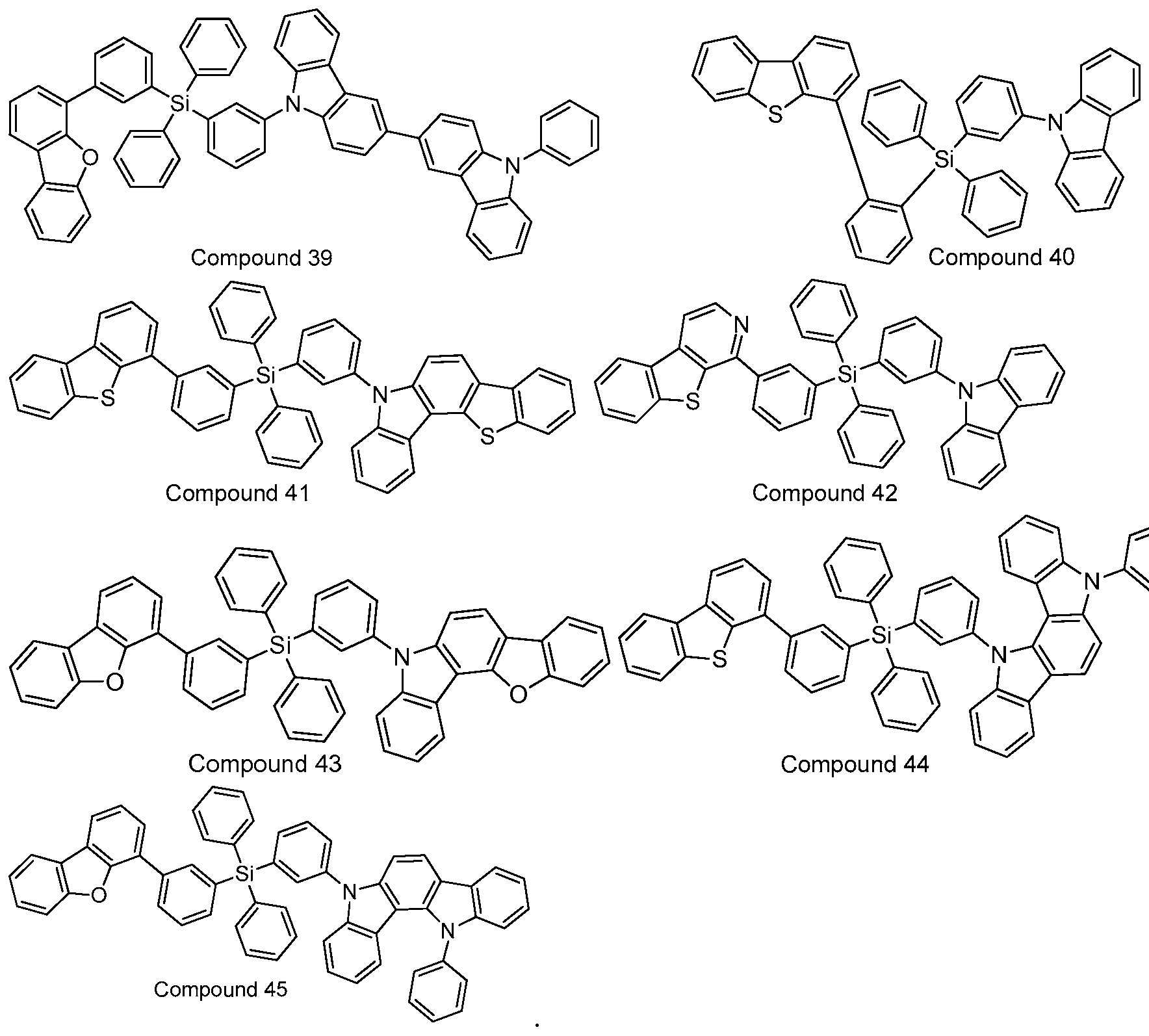
[0022] Non-limiting compounds are provided. In one aspect, the compound of Formula I is selected from Compound 1 - Compound 22. In Compound 1 - Compound 22, Y1 and Y2 are independently selected from the group consisting of O, S and Se, and Z is selected from the group consisting of Si and Ge. In another aspect, the compound of Formula I is selected from Compound 23 - Compound 45.
[0023] A first device is also provided. The first device comprises an organic light emitting device, and further comprises an anode, a cathode, and an organic layer, disposed between the anode and the cathode, comprising a compound having the Formula I:
Figure imgf000009_0001
Formula I,
Ar and Ar' are independently selected from the group consisting of phenyl, biphenyl, napthyl, dibenzothiolyl, and dibenzofuranyl, which are optionally further substituted. Z is selected from Si and Ge. Li comprises aryl or heteroaryl groups, and any heteroatoms in the heteroaryl groups are nitrogen. L2 is a single bond or comprises aryl or heteroaryl groups, and any heteroatoms in the heteroaryl groups are nitrogen. Li and L2 can be optionally further substituted. [0024] Group A contains a group selected from the group consisting of dibenzofuran, dibenzothiophene, azadibenzofuran, azadibenzothiophene, dibenzoselenophene and
azadibenzoselenophene, which are optionally further substituted, and wherein the substitution is optionally fused to at least one benzo ring. Group B contains a group selected from the group consisting of carbazole and azacarbazole, which are optionally further substituted, and wherein the substitution is optionally fused to the carbazole or azacarbazole group.
[0025] In one aspect, the organic layer is an emissive layer and the compound of formula I is a host. In another aspect, the organic layer further comprises an emissive dopant. In one aspect, the organic layer is deposited using a solution process. In one aspect, the emissive dopant is a transition metal complex having at least one ligand selected from the group consisting of:
Figure imgf000010_0001
Figure imgf000011_0001
wherein Ra, Rb, and Rc may represent mono, di, tri or tetra substitutions. Ra, Rb, and Rc are independently selected from the group consisting of hydrogen, deuterium, halide, alkyl, cycloalkyl, heteroalkyl, arylalkyl, alkoxy, aryloxy, amino, silyl, alkenyl, cycloalkenyl, heteroalkenyl, alkynyl, aryl, heteroaryl, acyl, carbonyl, carboxylic acids, ester, nitrile, isonitrile, sulfanyl, sulfinyl, sulfonyl, phosphino, and combinations thereof, and wherein two adjacent substituents of Ra, Rb, and Rc are optionally joined to form a fused ring.
[0026] In one aspect, the device further comprises a second organic layer that is a non- emissive layer and the compound having Formula I is a material in the second organic layer. In another aspect, the second organic layer is a blocking layer and the compound having Formula I is a blocking material in the second organic layer.
[0027] In one aspect, the first device is a consumer product. In another aspect, the first device is an organic light-emitting device. BRIEF DESCRIPTION OF THE DRAWINGS
[0028] FIG. 1 shows an organic light emitting device.
[0029] FIG. 2 shows an inverted organic light emitting device that does not have a separate electron transport layer.
[0030] FIG. 3 shows a compound of Formula I. [0031] FIG. 4 shows the layout of an OLED device. DETAILED DESCRIPTION
[0032] Generally, an OLED comprises at least one organic layer disposed between and electrically connected to an anode and a cathode. When a current is applied, the anode injects holes and the cathode injects electrons into the organic layer(s). The injected holes and electrons each migrate toward the oppositely charged electrode. When an electron and hole localize on the same molecule, an "exciton," which is a localized electron-hole pair having an excited energy state, is formed. Light is emitted when the exciton relaxes via a photoemissive mechanism. In some cases, the exciton may be localized on an excimer or an exciplex. Non-radiative mechanisms, such as thermal relaxation, may also occur, but are generally considered
undesirable.
[0033] The initial OLEDs used emissive molecules that emitted light from their singlet states ("fluorescence") as disclosed, for example, in U.S. Pat. No. 4,769,292, which is incorporated by reference in its entirety. Fluorescent emission generally occurs in a time frame of less than 10 nanoseconds. [0034] More recently, OLEDs having emissive materials that emit light from triplet states ("phosphorescence") have been demonstrated. Baldo et al., "Highly Efficient Phosphorescent Emission from Organic Electroluminescent Devices," Nature, vol. 395, 151-154, 1998; ("Baldo- I") and Baldo et al., "Very high-efficiency green organic light-emitting devices based on electrophosphorescence," Appl. Phys. Lett., vol. 75, No. 3, 4-6 (1999) ("Baldo-II"), which are incorporated by reference in their entireties. Phosphorescence is described in more detail in US Pat. No. 7,279,704 at cols. 5-6, which are incorporated by reference.
[0035] FIG. 1 shows an organic light emitting device 100. The figures are not necessarily drawn to scale. Device 100 may include a substrate 110, an anode 115, a hole injection layer 120, a hole transport layer 125, an electron blocking layer 130, an emissive layer 135, a hole blocking layer 140, an electron transport layer 145, an electron injection layer 150, a protective layer 155, and a cathode 160. Cathode 160 is a compound cathode having a first conductive layer 162 and a second conductive layer 164. Device 100 may be fabricated by depositing the layers described, in order. The properties and functions of these various layers, as well as example materials, are described in more detail in US 7,279,704 at cols. 6-10, which are incorporated by reference. [0036] More examples for each of these layers are available. For example, a flexible and transparent substrate-anode combination is disclosed in U.S. Pat. No. 5,844,363, which is incorporated by reference in its entirety. An example of a p-doped hole transport layer is m- MTDATA doped with F.sub.4-TCNQ at a molar ratio of 50: 1, as disclosed in U.S. Patent Application Publication No. 2003/0230980, which is incorporated by reference in its entirety. Examples of emissive and host materials are disclosed in U.S. Pat. No. 6,303,238 to Thompson et al., which is incorporated by reference in its entirety. An example of an n-doped electron transport layer is BPhen doped with Li at a molar ratio of 1 : 1 , as disclosed in U.S. Patent Application Publication No. 2003/0230980, which is incorporated by reference in its entirety. U.S. Pat. Nos. 5,703,436 and 5,707,745, which are incorporated by reference in their entireties, disclose examples of cathodes including compound cathodes having a thin layer of metal such as Mg:Ag with an overlying transparent, electrically-conductive, sputter-deposited ITO layer. The theory and use of blocking layers is described in more detail in U.S. Pat. No. 6,097,147 and U.S. Patent Application Publication No. 2003/0230980, which are incorporated by reference in their entireties. Examples of injection layers are provided in U.S. Patent Application Publication No. 2004/0174116, which is incorporated by reference in its entirety. A description of protective layers may be found in U.S. Patent Application Publication No. 2004/0174116, which is incorporated by reference in its entirety.
[0037] FIG. 2 shows an inverted OLED 200. The device includes a substrate 210, a cathode 215, an emissive layer 220, a hole transport layer 225, and an anode 230. Device 200 may be fabricated by depositing the layers described, in order. Because the most common OLED configuration has a cathode disposed over the anode, and device 200 has cathode 215 disposed under anode 230, device 200 may be referred to as an "inverted" OLED. Materials similar to those described with respect to device 100 may be used in the corresponding layers of device 200. FIG. 2 provides one example of how some layers may be omitted from the structure of device 100.
[0038] The simple layered structure illustrated in FIGS. 1 and 2 is provided by way of non- limiting example, and it is understood that embodiments of the invention may be used in connection with a wide variety of other structures. The specific materials and structures described are exemplary in nature, and other materials and structures may be used. Functional OLEDs may be achieved by combining the various layers described in different ways, or layers may be omitted entirely, based on design, performance, and cost factors. Other layers not specifically described may also be included. Materials other than those specifically described may be used. Although many of the examples provided herein describe various layers as comprising a single material, it is understood that combinations of materials, such as a mixture of host and dopant, or more generally a mixture, may be used. Also, the layers may have various sublayers. The names given to the various layers herein are not intended to be strictly limiting. For example, in device 200, hole transport layer 225 transports holes and injects holes into emissive layer 220, and may be described as a hole transport layer or a hole injection layer. In one embodiment, an OLED may be described as having an "organic layer" disposed between a cathode and an anode. This organic layer may comprise a single layer, or may further comprise multiple layers of different organic materials as described, for example, with respect to FIGS. 1 and 2.
[0039] Structures and materials not specifically described may also be used, such as OLEDs comprised of polymeric materials (PLEDs) such as disclosed in U.S. Pat. No. 5,247,190 to Friend et al., which is incorporated by reference in its entirety. By way of further example, OLEDs having a single organic layer may be used. OLEDs may be stacked, for example as described in U.S. Pat. No. 5,707,745 to Forrest et al, which is incorporated by reference in its entirety. The OLED structure may deviate from the simple layered structure illustrated in FIGS. 1 and 2. For example, the substrate may include an angled reflective surface to improve out- coupling, such as a mesa structure as described in U.S. Pat. No. 6,091,195 to Forrest et al, and/or a pit structure as described in U.S. Pat. No. 5,834,893 to Bulovic et al, which are incorporated by reference in their entireties.
[0040] Unless otherwise specified, any of the layers of the various embodiments may be deposited by any suitable method. For the organic layers, preferred methods include thermal evaporation, ink-jet, such as described in U.S. Pat. Nos. 6,013,982 and 6,087,196, which are incorporated by reference in their entireties, organic vapor phase deposition (OVPD), such as described in U.S. Pat. No. 6,337,102 to Forrest et al, which is incorporated by reference in its entirety, and deposition by organic vapor jet printing (OVJP), such as described in U.S. patent application Ser. No. 10/233,470, which is incorporated by reference in its entirety. Other suitable deposition methods include spin coating and other solution based processes. Solution based processes are preferably carried out in nitrogen or an inert atmosphere. For the other layers, preferred methods include thermal evaporation. Preferred patterning methods include deposition through a mask, cold welding such as described in U.S. Pat. Nos. 6,294,398 and 6,468,819, which are incorporated by reference in their entireties, and patterning associated with some of the deposition methods such as ink-jet and OVJD. Other methods may also be used. The materials to be deposited may be modified to make them compatible with a particular deposition method. For example, substituents such as alkyl and aryl groups, branched or unbranched, and preferably containing at least 3 carbons, may be used in small molecules to enhance their ability to undergo solution processing. Substituents having 20 carbons or more may be used, and 3-20 carbons is a preferred range. Materials with asymmetric structures may have better solution processibility than those having symmetric structures, because asymmetric materials may have a lower tendency to recrystallize. Dendrimer substituents may be used to enhance the ability of small molecules to undergo solution processing. [0041] Devices fabricated in accordance with embodiments of the invention may be incorporated into a wide variety of consumer products, including flat panel displays, computer monitors, televisions, billboards, lights for interior or exterior illumination and/or signaling, heads up displays, fully transparent displays, flexible displays, laser printers, telephones, cell phones, personal digital assistants (PDAs), laptop computers, digital cameras, camcorders, viewfmders, micro-displays, vehicles, a large area wall, theater or stadium screen, or a sign. Various control mechanisms may be used to control devices fabricated in accordance with the present invention, including passive matrix and active matrix. Many of the devices are intended for use in a temperature range comfortable to humans, such as 18 degrees C. to 30 degrees C, and more preferably at room temperature (20-25 degrees C). [0042] The materials and structures described herein may have applications in devices other than OLEDs. For example, other optoelectronic devices such as organic solar cells and organic photodetectors may employ the materials and structures. More generally, organic devices, such as organic transistors, may employ the materials and structures. [0043] The terms halo, halogen, alkyl, cycloalkyl, alkenyl, alkynyl, arylkyl, heterocyclic group, aryl, aromatic group, and heteroaryl are known to the art, and are defined in US 7,279,704 at cols. 31-32, which are incorporated herein by reference.
[0044] A compound of Formula I is provided.
Figure imgf000016_0001
Formula I,
In one embodiment, Ar and Ar' are independently selected from the group consisting of phenyl, biphenyl, napthyl, dibenzothiolyl, and dibenzofuranyl, which are optionally further substituted. Z is selected from Si and Ge. Li comprises aryl or heteroaryl groups, and any heteroatoms in the heteroaryl groups are nitrogen. L2 is a single bond or comprises aryl or heteroaryl groups, and any heteroatoms in the heteroaryl groups are nitrogen. Li and L2 can be optionally further substituted. In one embodiment, the substituents on Lls L2, Ar, and Ar' can be hydrogen, deuterium, halide, alkyl, cycloalkyl, heteroalkyl, arylalkyl, alkoxy, aryloxy, amino, silyl, alkenyl, cycloalkenyl, heteroalkenyl, alkynyl, aryl, heteroaryl, acyl, carbonyl, carboxylic acids, ester, nitrile, isonitrile, sulfanyl, sulfinyl, sulfonyl, phosphino, and combinations thereof. [0045] An "aryl" group is an aromatic all carbon group, which can contain one or more fused rings within it. Merely by way of example, and without any limitation, exemplary aryl groups can be phenyl, naphthalene, phenanthrene, corannulene, etc. A "heteroaryl" group is an "aryl" group containing at least one heteroatom. Merely by way of example, and without any limitation, exemplary heteroaryl groups can be pyridine, quinoline, phenanthroline,
azacorannulene, etc. Both "aryl" and "heteroaryl" groups in Li and L2 can have multiple attachment points connecting them to other fragments. Li and L2 can contain any desired number of aryl or heteroaryl groups.
[0046] Group A contains a group selected from the group consisting of dibenzofuran, dibenzothiophene, azadibenzofuran, azadibenzothiophene, dibenzoselenophene and
azadibenzoselenophene, which are optionally further substituted, and wherein the substitution is optionally fused to at least one benzo ring. Group B contains a group selected from the group consisting of carbazole and azacarbazole, which are optionally further substituted, and wherein the substitution is optionally fused to the carbazole or azacarbazole group. [0047] In one embodiment, A is selected from the group consisting of:
Figure imgf000017_0001
In another embodiment, B is selected from the group consisting of:
Figure imgf000018_0001
Yi and Y2 are independently selected from the group consisting of O, S, and Se. Xi to Xio are independently selected from the group consisting of CR and N, and wherein each benzo ring contains at most one N. R is selected from the group consisting of hydrogen, deuterium, halide, alkyl, cycloalkyl, heteroalkyl, arylalkyl, alkoxy, aryloxy, amino, silyl, alkenyl, cycloalkenyl, heteroalkenyl, alkynyl, aryl, heteroaryl, acyl, carbonyl, carboxylic acids, ester, nitrile, isonitrile, sulfanyl, sulfmyl, sulfonyl, phosphino, and combinations thereof.
[0048] In one embodiment, Li and L2 are independently selected from the group consisting of:
Figure imgf000019_0001
[0049] In one embodiment, L2 is a single bond. In another embodiment, Li and L2 contain at least one phenyl bonded directly to Z. The dashed lines in the chemical structures disclosed herein represent a bond through any position on that group capable of forming a single bond with another atom.
[0050] In one embodiment, Ar and Ar' are phenyl. In another embodiment, Ar, Ar', A and B are independently substituted with at least one group selected from the group consisting of hydrogen, deuterium, halide, alkyl, cycloalkyl, heteroalkyl, arylalkyl, alkoxy, aryloxy, amino, silyl, alkenyl, cycloalkenyl, heteroalkenyl, alkynyl, aryl, heteroaryl, acyl, carbonyl, carboxylic acids, ester, nitrile, isonitrile, sulfanyl, sulfinyl, sulfonyl, phosphino, and combinations thereof.
[0051] In one embodiment, "aryl" comprises phenyl, biphenyl, triphenyl, terphenyl, naphthalene, phenalene, phenanthrene, fluorene or chrysene, and in another embodiment, "heteroaryl" comprises dibenzothiophene, dibenzofuran, benzofuran, benzothiophene, pyrazole, imidazole, triazole, oxazole, thiazole, oxadiazole, oxatriazole, dioxazole, thiadiazole, pyridine, pyridazine, pyrimidine, pyrazine, triazine, indole, azaindole, benzimidazole, indazole, benzoxazole, benzisoxazole, benzothiazole, quinoline, isoquinoline, cinnoline, quinazoline, quinoxaline, naphthyridine, phthalazine, pteridine, xanthene, phenothiazine, phenoxazine, benzofuropyridine, furodipyridine, benzothienopyridine and thienodipyridine.
[0052] The novel compounds of Formula I disclosed herein contain of two different moieties, groups A and B, connected with an arylsilane or arylgermane spacer, resulting in an asymmetric structure. By "asymmetric" it is meant that groups A and B, as described above, have different structures. The compounds of Formula I have a number of advantageous properties when used in OLED devices. Firstly, inclusion of two distinct moieties allows fine-tuning the energy levels of the resultant compound, which may facilitate charge injection from adjacent layers and modulate charge trapping by the emitter dopants. Secondly, the two different moieties can be independently selected to have as electron and/or hole transport properties, yielding compounds with bipolar charge transport characteristics. These characteristics may not only suppresses operation voltage but also balance electron and hole fluxes to achieve an extended charge recombination zone. Thirdly, the arylsilane and arylgermane spacers break the conjugation between groups A and B, retaining high triplet energy for the entire molecule, and thus effectively reducing quenching.
[0053] The compounds of Formula I have additional advantages over known symmetric analogs because compounds of Formula I are less prone to crystallization. As a result, compounds of Formula I possess improved film uniformity, which, without being bound by theory, is believed to be a result of reduction in phase separation between the emitters and host materials. The novel compounds of Formula I can be used to improve OLED device performance parameters, such as emission spectrum line shape, efficiency and lifetime.
Furthermore, compounds of Formula I also tend to be soluble in organic solvents such as toluene, xylene, and 3-phenoxytoluene, and are amenable to solution processing which is highly desirable for low-cost lighting applications.
[0054] In one embodiment, the compound of Formula I is selected from the group consisting of:
Figure imgf000021_0001
Figure imgf000022_0001
Figure imgf000023_0001
Yi and Y2 are independently selected from the group consisting of O, S and Se. Z is selected from the group consisting of Si and Ge.
[0055] In another embodiment, the compound of Formula I is selected from the group consisting of:
Figure imgf000023_0002
Figure imgf000024_0001
Figure imgf000025_0001
Figure imgf000025_0002
[0056] A first device is also provided. The first device comprises an organic light emitting device, and further comprises an anode, a cathode, and an organic layer, disposed between the anode and the cathode, comprising a compound having the Formula I: Ar
A L, Z L2 B
1
Ar' , Formula I,
Ar and Ar' are independently selected from the group consisting of phenyl, biphenyl, napthyl, dibenzothiolyl, and dibenzofuranyl, which are optionally further substituted. Z is selected from Si and Ge. Li comprises aryl or heteroaryl groups, and any heteroatoms in the heteroaryl groups are nitrogen. L2 is a single bond or comprises aryl or heteroaryl groups, and any heteroatoms in the heteroaryl groups are nitrogen. Li and L2 can be optionally further substituted. In one embodiment, the substituents on Lls L2, Ar, and Ar' can be hydrogen, deuterium, halide, alkyl, cycloalkyl, heteroalkyl, arylalkyl, alkoxy, aryloxy, amino, silyl, alkenyl, cycloalkenyl, heteroalkenyl, alkynyl, aryl, heteroaryl, acyl, carbonyl, carboxylic acids, ester, nitrile, isonitrile, sulfanyl, sulfmyl, sulfonyl, phosphino, and combinations thereof.
[0057] Group A contains a group selected from the group consisting of dibenzofuran, dibenzothiophene, azadibenzofuran, azadibenzothiophene, dibenzoselenophene and
azadibenzoselenophene, which are optionally further substituted, and wherein the substitution is optionally fused to at least one benzo ring. Group B contains a group selected from the group consisting of carbazole and azacarbazole, which are optionally further substituted, and wherein the substitution is optionally fused to the carbazole or azacarbazole group.
[0058] In one embodiment, the organic layer is an emissive layer and the compound of Formula I is a host. In another embodiment, the organic layer further comprises an emissive dopant. In one embodiment, the emissive dopant is a transition metal complex having at least one ligand selected from the group consisting of:
Figure imgf000026_0001
Figure imgf000027_0001
wherein Ra, Rb, and Rc may represent mono, di, tri or tetra substitutions. Ra, Rb, and Rc are independently selected from the group consisting of hydrogen, deuterium, halide, alkyl, cycloalkyl, heteroalkyl, arylalkyl, alkoxy, aryloxy, amino, silyl, alkenyl, cycloalkenyl, heteroalkenyl, alkynyl, aryl, heteroaryl, acyl, carbonyl, carboxylic acids, ester, nitrile, isonitrile, sulfanyl, sulfinyl, sulfonyl, phosphino, and combinations thereof, and wherein two adjacent substituents of Ra, Rb, and Rc are optionally joined to form a fused ring. [0059] In one embodiment, the device further comprises a second organic layer that is a non- emissive layer and the compound having Formula I is a material in the second organic layer. In another embodiment, the second organic layer is a blocking layer and the compound having Formula I is a blocking material in the second organic layer. In one embodiment, the organic layer is deposited using a solution process.
[0060] In one embodiment, the first device is a consumer product. In another embodiment, the first device is an organic light-emitting device.
[0061] Device Examples
[0062] The structures of the materials used in the device examples is show in Table 1 below. [0063] TABLE 1.
Figure imgf000028_0001
[0064] The organic stack of the OLED device used in the Examples and Cmparative Device Examples has the following structure: from the ITO surface, 100 A of Compound HIL as the hole injection layer, 300 A of NPD as the hole transporting layer (HTL), 300 A of a compound of Formula I, CC-1 or CC-2 doped with 15 wt% of Compound D as the emissive layer (EML), 50 A of Compound BL as the Blocking Layer (BL) and 400 A of Alq as the ETL1. The device structure is shown in FIG. 4.
[0065] Comparative Compounds CC-1 and CC-2 have the following structures:
Figure imgf000029_0001
ABLE 2.
Figure imgf000029_0002
Device Compound Compound
0.176 0.387 474 6.5 45.7 20.3 22.0 55 Example 16 38 BL
Device Compound Compound
0.174 0.385 472 7.1 43 19.2 19.1 75 Example 17 23 23
Device Compound Compound
0.171 0.371 474 7.5 41.3 19.0 17.2 80 Example 18 24 24
Device Compound Compound
0.177 0.389 474 7.6 40.5 17.9 16.8 78 Example 19 25 25
Device Compound Compound
0.186 0.426 476 9.6 43.7 18.1 14.3 83 Example 20 26 26
Device Compound Compound
0.176 0.387 474 8.2 40.1 17.8 15.4 87 Example 21 27 27
Device Compound Compound
0.174 0.380 474 7.5 43.1 19.4 18.0 86 Example 22 28 28
Device Compound Compound
0.173 0.378 474 7.3 40.8 18.5 17.5 67 Example 23 29 29
Device Compound Compound
0.172 0.376 474 7.6 43.3 19.7 17.9 47 Example 24 30 30
Device Compound Compound
0.174 0.383 474 7.4 42.2 19.0 17.9 60 Example 25 31 31
Device Compound Compound
0.175 0.390 474 8.2 40.1 17.9 15.4 30 Example 26 32 32
Device Compound Compound
0.180 0.402 474 8.6 37.5 16.3 13.7 125 Example 27 33 33
Device Compound Compound
0.173 0.380 474 8.3 39.7 17.9 15.1 88 Example 28 34 34
Device Compound Compound
0.181 0.408 476 7.1 43.6 18.8 19.3 33 Example 29 35 35
Device Compound Compound
0.177 0.402 474 7.2 46.3 20.1 20.2 39 Example 30 36 36
Device Compound Compound
0.177 0.390 474 7.1 43 19.1 19.0 40 Example 31 37 37
Device Compound Compound
0.173 0.381 474 7.8 42.4 19.1 17.0 54 Example 32 38 38
Comparative
Compound
Device CC-1 0.177 0.387 474 6.8 42.5 18.8 19.7 40
BL
Example 1
Comparative
Compound
Device CC-2 0.179 0.396 474 7.2 35.4 15.4 15.5 176
BL
Example 2
[0066] Table 2 is a summary of the device data. The devices with aryl silane hosts show high efficiency and long lifetimes. Compared to the host without aryl silane moiety, CC-2, the aryl silane hosts demonstrates much improved efficiency (Device Examples 1-16 vs. Comparative Device Example 2). Without being bound by theory, these results are attributable in part to the breakage of conjugation by the silane bridge and retention of high triplet energy for individual molecules. Additionally, the steric hindrance introduced by the tetraphenylsilane unit can also prevent unfavorable intermolecular stacking that can decrease the triplet energy in the solid state. A high triplet energy of the host effectively confines the excitons on emitters, leading to high efficiency.
[0067] Furthermore, devices with the asymmetric aryl silane hosts have comparable to much improved lifetime than those with the symmetric aryl silane hosts (Device Examples 1-16 vs Comparative Device Example 1). This is attributable to the asymmetric nature of, for example, Compound 23, which not only lowers the operation voltage, but also helps to balance charge fluxes. The balanced electron/hole fluxes spread the charge recombination zone, which preserves a high efficiency at high brightness by suppressing or reducing exciton quenching. An expanded charge recombination zone also extends the device lifetime by allowing a larger population of molecules to have charge transport, exciton formation, and light emission roles. It is also demonstrated that the compounds of Formula I are useful as blocking layer components (Device Examples 17-32), producing OLEDs having high efficiencies and long lifetimes. Since compounds of Formula I can serve both as hosts and hole blocking layers, these materials are expected to reduce device fabrication cost.
COMBINATION WITH OTHER MATERIALS [0068] The materials described herein as useful for a particular layer in an organic light emitting device may be used in combination with a wide variety of other materials present in the device. For example, emissive dopants disclosed herein may be used in conjunction with a wide variety of hosts, transport layers, blocking layers, injection layers, electrodes and other layers that may be present. The materials described or referred to below are non-limiting examples of materials that may be useful in combination with the compounds disclosed herein, and one of skill in the art can readily consult the literature to identify other materials that may be useful in combination.
HIL/HTL: [0069] A hole injecting/transporting material to be used in the present invention is not particularly limited, and any compound may be used as long as the compound is typically used as a hole injecting/transporting material. Examples of the material include, but not limit to: a phthalocyanine or porphryin derivative; an aromatic amine derivative; an indolocarbazole derivative; a polymer containing fluorohydrocarbon; a polymer with conductivity dopants; a conducting polymer, such as PEDOT/PSS; a self-assembly monomer derived from compounds such as phosphonic acid and sliane derivatives; a metal oxide derivative, such as MoOx; a p-type semiconducting organic compound, such as 1,4,5,8,9,12-Hexaazatriphenylenehexacarbonitrile; a metal complex, and a cross-linkable compounds.
[0070] Examples of aromatic amine derivatives used in HIL or HTL include, but not limit to the following general structures:
Figure imgf000032_0001
Ar4 .Ar°
Ar Ar4
\ Ar1
N— Ar1— N
Λ \ ,
Ar Ar
/ \ Ar6^ ^Ar2 \r3 ^Ar9
Ar6— N N— Ar9 N
\ / I I
Ar7 Ar8 Ar7 Ar8
[0071] Each of Ar1 to Ar9 is selected from the group consisting aromatic hydrocarbon cyclic compounds such as benzene, biphenyl, triphenyl, triphenylene, naphthalene, anthracene, phenalene, phenanthrene, fluorene, pyrene, chrysene, perylene, azulene; group consisting aromatic heterocyclic compounds such as dibenzothiophene, dibenzofuran, dibenzoselenophene, furan, thiophene, benzofuran, benzothiophene, benzoselenophene, carbazole, indolocarbazole, pyridylindole, pyrrolodipyridine, pyrazole, imidazole, triazole, oxazole, thiazole, oxadiazole, oxatriazole, dioxazole, thiadiazole, pyridine, pyridazine, pyrimidine, pyrazine, triazine, oxazine, oxathiazine, oxadiazine, indole, benzimidazole, indazole, indoxazine, benzoxazole,
benzisoxazole, benzothiazole, quinoline, isoquinoline, cinnoline, quinazoline, quinoxaline, naphthyridine, phthalazine, pteridine, xanthene, acridine, phenazine, phenothiazine, phenoxazine, benzofuropyridine, furodipyridine, benzothienopyridine, thienodipyridine, benzoselenophenopyridine, and selenophenodipyridine; and group consisting 2 to 10 cyclic structural units which are groups of the same type or different types selected from the aromatic hydrocarbon cyclic group and the aromatic heterocyclic group and are bonded to each other directly or via at least one of oxygen atom, nitrogen atom, sulfur atom, silicon atom, phosphorus atom, boron atom, chain structural unit and the aliphatic cyclic group. Wherein each Ar is further substituted by a substituent selected from the group consisting of hydrogen, deuterium, halide, alkyl, cycloalkyl, heteroalkyl, arylalkyl, alkoxy, aryloxy, amino, silyl, alkenyl, cycloalkenyl, heteroalkenyl, alkynyl, aryl, heteroaryl, acyl, carbonyl, carboxylic acids, ester, nitrile, isonitrile, sulfanyl, sulfinyl, sulfonyl, phosphino, and combinations thereof.
[0072] In one aspect, Ar1 to Ar9 is independently selected from the group consisting of:
Figure imgf000033_0001
[0073] k is an integer from 1 to 20; X1 to X8 is C (including CH) or N; Ar1 has the same group defined above.
[0074] Examples of metal complexes used in HIL or HTL include, but not limit to the following general formula:
Figure imgf000033_0002
[0075] M is a metal, having an atomic weight greater than 40; (Y^Y2) is a bindentate ligand, Yl and Y2 are independently selected from C, N, O, P, and S; L is an ancillary ligand; m is an integer value from 1 to the maximum number of ligands that may be attached to the metal; and m+n is the maximum number of ligands that may be attached to the metal. [0076] In one aspect, (Y^Y2) is a 2-phenylpyridine derivative.
[0077] In another aspect, (Y^Y2) is a carbene ligand.
[0078] In another aspect, M is selected from Ir, Pt, Os, and Zn.
[0079] In a further aspect, the metal complex has a smallest oxidation potential in solution vs. Fc+/Fc couple less than about 0.6 V.
Host:
[0080] The light emitting layer of the organic EL device of the present invention preferably contains at least a metal complex as light emitting material, and may contain a host material using the metal complex as a dopant material. Examples of the host material are not particularly limited, and any metal complexes or organic compounds may be used as long as the triplet energy of the host is larger than that of the dopant.
[0081] Examples of metal complexes used as host are preferred to have the following general formula:
Figure imgf000034_0001
[0082] M is a metal; (Y3-Y4) is a bindentate ligand, Y3 and Y4 are independently selected from C, N, O, P, and S; L is an ancillary ligand; m is an integer value from 1 to the maximum number of ligands that may be attached to the metal; and m+n is the maximum number of ligands that may be attached to the metal.
[0083] In one aspect, the metal complexes are:
Figure imgf000034_0002
[0084] (O-N) is a bidentate ligand, having metal coordinated to atoms O and N.
[0085] In another aspect, M is selected from Ir and Pt.
[0086] In a further aspect, (Y3-Y4) is a carbene ligand. [0087] Examples of organic compounds used as host are selected from the group consisting aromatic hydrocarbon cyclic compounds such as benzene, biphenyl, triphenyl, triphenylene, naphthalene, anthracene, phenalene, phenanthrene, fluorene, pyrene, chrysene, perylene, azulene; group consisting aromatic heterocyclic compounds such as dibenzothiophene, dibenzofuran, dibenzoselenophene, furan, thiophene, benzofuran, benzothiophene, benzoselenophene, carbazole, indolocarbazole, pyridylindole, pyrrolodipyridine, pyrazole, imidazole, triazole, oxazole, thiazole, oxadiazole, oxatriazole, dioxazole, thiadiazole, pyridine, pyridazine, pyrimidine, pyrazine, triazine, oxazine, oxathiazine, oxadiazine, indole, benzimidazole, indazole, indoxazine, benzoxazole, benzisoxazole, benzothiazole, quinoline, isoquinoline, cinnoline, quinazoline, quinoxaline, naphthyridine, phthalazine, pteridine, xanthene, acridine, phenazine, phenothiazine, phenoxazine, benzofuropyridine, furodipyridine, benzothienopyridine, thienodipyridine, benzoselenophenopyridine, and selenophenodipyridine; and group consisting 2 to 10 cyclic structural units which are groups of the same type or different types selected from the aromatic hydrocarbon cyclic group and the aromatic heterocyclic group and are bonded to each other directly or via at least one of oxygen atom, nitrogen atome, sulfur atom, silicon atom, phosphorus atom, boron atom, chain structural unit and the aliphatic cyclic group. Wherein each group is further substituted by a substituent selected from the group consisting of hydrogen, deuterium, halide, alkyl, cycloalkyl, heteroalkyl, arylalkyl, alkoxy, aryloxy, amino, silyl, alkenyl, cycloalkenyl, heteroalkenyl, alkynyl, aryl, heteroaryl, acyl, carbonyl, carboxylic acids, ester, nitrile, isonitrile, sulfanyl, sulfinyl, sulfonyl, phosphino, and combinations thereof.
[0088] In one aspect, host compound contains at least one of the following groups in the molecule:
Figure imgf000036_0001
[0089] R1 to R7 is independently selected from the group consisting of hydrogen, alkyl, alkoxy, amino, alkenyl, alkynyl, arylalkyl, heteroalkyl, aryl and heteroaryl, when it is aryl or heteroaryl, it has the similar definition as Ar's mentioned above. [0090] k is an integer from 0 to 20.
[0091] X1 to X8 is selected from C (including CH) or N.
HBL:
[0092] A hole blocking layer (HBL) may be used to reduce the number of holes and/or excitons that leave the emissive layer. The presence of such a blocking layer in a device may result in substantially higher efficiencies as compared to a similar device lacking a blocking layer. Also, a blocking layer may be used to confine emission to a desired region of an OLED.
[0093] In one aspect, compound used in HBL contains the same molecule used as host described above. [0094] In another aspect, compound used in HBL contains at least one of the following groups in the molecule:
Figure imgf000037_0001
[0095] k is an integer from 0 to 20; L is an ancillary ligand, m is an integer from 1 to 3. ETL:
[0096] Electron transport layer (ETL) may include a material capable of transporting electrons. Electron transport layer may be intrinsic (undoped), or doped. Doping may be used to enhance conductivity. Examples of the ETL material are not particularly limited, and any metal complexes or organic compounds may be used as long as they are typically used to transport electrons.
[0097] In one aspect, compound used in ETL contains at least one of the following groups in the molecule:
Figure imgf000037_0002
[0098] R1 is selected from the group consisting of hydrogen, alkyl, alkoxy, amino, alkenyl, alkynyl, arylalkyl, heteroalkyl, aryl and heteroaryl, when it is aryl or heteroaryl, it has the similar definition as Ar's mentioned above.
[0099] Ar1 to Ar3 has the similar definition as Ar's mentioned above. [0100] k is an integer from 0 to 20.
[0101] X1 to X8 is selected from C (including CH) or N.
[0102] In another aspect, the metal complexes used in ETL contains, but not limit to the following general formula:
Figure imgf000038_0001
[0103] (O-N) or (N-N) is a bidentate ligand, having metal coordinated to atoms O, N or N, N; L is an ancillary ligand; m is an integer value from 1 to the maximum number of ligands that may be attached to the metal.
[0104] In any above-mentioned compounds used in each layer of the OLED device, the hydrogen atoms can be partially or fully deuterated.
[0105] In addition to and / or in combination with the materials disclosed herein, many hole injection materials, hole transporting materials, host materials, dopant materials, exiton/hole blocking layer materials, electron transporting and electron injecting materials may be used in an OLED. Non- limiting examples of the materials that may be used in an OLED in combination with materials disclosed herein are listed in Table 3 below. Table 3 lists non-limiting classes of materials, non-limiting examples of compounds for each class, and references that disclose the materials.
Figure imgf000038_0002
Figure imgf000038_0003
Figure imgf000039_0001
Figure imgf000040_0001
Figure imgf000041_0001
Figure imgf000042_0001
Metal Appl. Phys. Lett. 90, phenoxybenzothiazole 123509 (2007) compounds
Conjugated oligomers and Org. Electron. 1, 15 polymers (2000)
(e.g., polyfluorene)
Aromatic fused rings WO2009066779,
WO2009066778, WO2009063833, US20090045731, US20090045730, WO2009008311, US20090008605, US20090009065
Zinc complexes WO2009062578
Figure imgf000043_0001
Green hosts
Arylcarbazoles Appl. Phys. Lett. 78,
1622 (2001)
US20030175553
WO2001039234
Aryltriphenylene US20060280965 compounds
Figure imgf000044_0001
Figure imgf000045_0001
Figure imgf000046_0001
Figure imgf000047_0001
Figure imgf000048_0001
Figure imgf000049_0001
Figure imgf000050_0001
Figure imgf000051_0001
Figure imgf000052_0001
Figure imgf000053_0001
Figure imgf000054_0001
Figure imgf000055_0001
Figure imgf000056_0001
US20090179554
Aza triphenylene US20090115316 derivatives
Anthracene-benzothiazole Appl. Phys. Lett. 89, compounds 063504 (2006)
Metal 8-hydroxyquinolates Appl. Phys. Lett. 51, (e.g., Alq3, Zrq4) 913 (1987)
3 US7230107
Metal Chem. Lett. 5, 905 hydroxybenoquinolates (1993)
2
Bathocuprine compounds Appl. Phys. Lett. 91, such as BCP, BPhen, etc 263503 (2007)
Appl. Phys. Lett. 79, 449 (2001)
5 -member ring electron Appl. Phys. Lett. 74, deficient heterocycles 865 (1999)
(e.g.,triazole, oxadiazole,
imidazole,
benzoimidazole)
N-N Appl. Phys. Lett. 55,
1489 (1989)
Figure imgf000058_0001
EXPERIMENTAL [0106] Chemical abbreviations used throughout this document are as follows: dba is dibenzylideneacetone, EtOAc is ethyl acetate, PPh3 is triphenylphosphine, dppf is Ι,Γ- bis(diphenylphosphino)ferrocene, DCM is dichloromethane, SPhos is dicyclohexyl(2',6'- dimethoxy-[l,l'-biphenyl]-3-yl)phosphine, THF is tetrahydrofuran. [0107] Example 1 : Synthesis of Compound 23
Figure imgf000059_0001
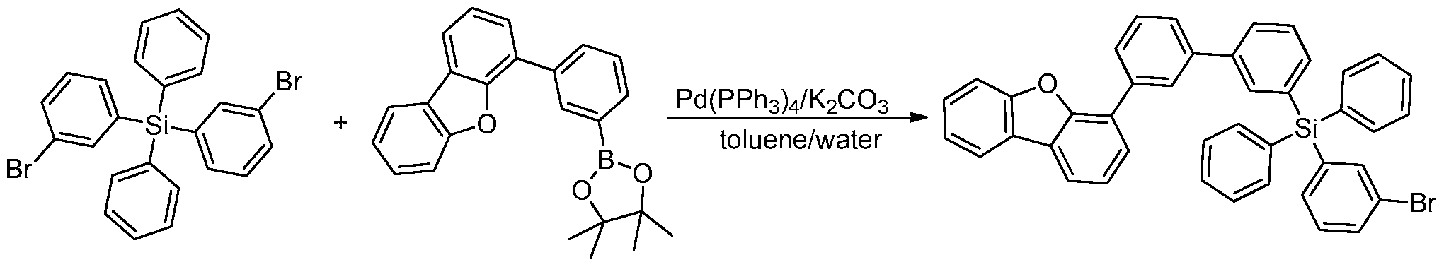
[0108] Butyllithium (53.2 mL, 133 mmol, 2.5M in hexane) was added dropwise into a solution of 1,3-dibromobenzene (15.38 mL, 127 mmol) in ether (300 mL) at -78 °C. The reaction mixture was stirred at this temperature before dichlorodiphenylsilane (11.90 mL, 57.8 mmol) in ether (20 mL) was added dropwise to yield a clear yellow solution. The solution was allowed to warm up to room temperature overnight and quenched with water. The organic phase was washed with brine and water, dried over Na2S04. Upon evaporation of the solvent, the residue was purified by column chromatography on silica gel with hexane/DCM (9.8/0.2, v/v) as eluent, and recrystallized from methanol to yield bis(3-bromophenyl)diphenylsilane (25 g, 87 %) as white crystals.
Figure imgf000059_0002
[0109] A mixture solution of dibenzo[^<i]thiophen-4-boronic acid (1.84 g, 8.04 mmol), bis(3- bromophenyl)diphenylsilane (9.97 g, 20.17 mmol), Pd(PPh3)4 (0.19 g, 0.16 mmol) and potassium carbonate (6.69 g, 48.4 mmol, ) in toluene (60 mL) and water (20 mL) was heated at 100°C under nitrogen overnight. After cooling to room temperature, the reaction mixture was quenched with water, extracted with DCM, washed with brine and water, and dried over Na2S04. Upon evaporation of the solvent, the residue was purified by column chromatography on silica gel with hexane:DCM (9.5:0.5 to 9:1 , v/v) as eluent. The crude product was dissolved in DCM, precipitated with methanol, and filtered to yield (3 -bromophenyl)(3 -(dibenzo [¾,d]thiophen-4- yl)phenyl) diphenylsilane (3.0 g, 62%) as a white solid.
Figure imgf000060_0001
[0110] A mixture solution of (3 -bromophenyl)(3 -(dibenzo [b, ]thiophen-4- yl)phenyl)diphenylsilane (3 g, 5.02 mmol), 9-(3-(4,4,5,5-tetramethyl-l,3,2-dioxaborolan-2- yl)phenyl)-9H-carbazole (2.039 g, 5.52 mmol), tris(dibenzylideneacetone)dipalladium (0) (Pd2(dba)3) (0.092 g, 0.100 mmol), dicyclohexyl(2',6'-dimethoxy-[l, -biphenyl]-3-yl)phosphine (SPhos) (0.082 g, 0.201 mmol), and potassium phosphate tribasic (K3P04) (1.066 g, 5.02 mmol) in toluene (40 mL) and water (4 mL) was heated at 100 °C under nitrogen overnight. The reaction mixture was quenched with water, extracted with DCM, washed with brine and water, and dried over Na2S04. Upon evaporation of the solvent, the residue was purified by column chromatography with hexane:DCM(9.25:0.75, v/v) as eluent. The crude product was dissolved in DCM, precipitated with methanol, and filtered to yield Compound 23 (2.2 g, 66%) as a colorless glass.
[0111] Example 2: Synthesis of Compound 24
Figure imgf000060_0002
[0112] A suspension of (3 -bromophenyl)(3 -(dibenzo [£,d]thiophen-4-yl)phenyl)diphenylsilane (3.5 g, 5.86 mmol), 9H-carbazole (0.979 g, 5.86 mmol), Pd2(dba)3 (0.107 g, 0.117 mmol), SPhos (0.096 g, 0.234 mmol), and sodium tert-butoxide (0.563 g, 5.86 mmol) in m-xylene (50 mL) was refluxed under nitrogen overnight. After cooling to room temperature, the reaction mixture was filtered through a short plug of Celite, and washed with toluene. The combined organic solution was washed with water and dried over Na2S04. Upon evaporation of the solvent, the crude product was purified by column chromatography on silica gel with hexane:DCM (9.25:0.75, v/v) as eluent. The crude product was dissolved in DCM, precipitated with methanol, and filtered to yield Compound 24 (2.5 g, 62%) as a colorless glass.
[0113] Example 3: Synthesis of Compound 25
Figure imgf000061_0001
[0114] A suspension of (3-bromophenyl)(3-(dibenzo[^<i]thiophen-4-yl)phenyl)diphenylsilane (3.5 g, 5.86 mmol), 9H-3,9*-bicarbazole (1.947 g, 5.86 mmol), Pd2(dba)3 (0.107 g, 0.117 mmol), SPhos (0.096 g, 0.234 mmol), and sodium tert-butoxide (0.563 g, 5.86 mmol) was added to m- xylene (100 mL) and refluxed under nitrogen overnight. After cooling to room temperature, the reaction mixture was filtered through a short plug of Celite and washed with toluene. T he combined organic solution was washed with water, dried over Na2S04. Upon evaporation of the solvent, the residue was purified by column chromatography on silica gel with hexane:DCM (8.5: 1.5, v/v) as eluent. The crude product was dissolved in DCM, precipitated with ethanol, and filtered to yield Compound 25 (3.0 g, 60%) as a colorless glass.
[0115] Example 4: Synthesis of Compound 26
Figure imgf000061_0002
[0116] A mixture solution of 2-(3-(dibenzo[^<i]thiophen-4-yl)phenyl)-4,4,5,5-tetramethyl-
1,3,2-dioxaborolane (6.0 g, 15.53 mmol), bis(3-bromophenyl)diphenylsilane (19.19 g, 38.8 mmol), Pd2(dba)3 (0.28 g, 0.31 mmol), SPhos (0.26 g, 0.62 mmol) and K3P04 (3.30 g, 15.53 mmol) in xylene (150 mL) and water (15 mL) was refluxed under nitrogen at 120 °C overnight. After cooling to room temperature, the reaction mixture was quenched with water, extracted with DCM, washed with brine and water, and dried over Na2S04. Upon evaporation of the solvent, the residue was purified by column chromatography on silica gel with hexane:DCM (9.5:0.5 to 9: 1, v/v) as eluent. The crude product was dissolved in DCM, precipitated with methanol, and filtered to yield (3-bromophenyl)(3'-(dibenzo[^<i]thiophen-4-yl)-[l, -biphenyl]-3- yl)diphenylsilane (3.2 g, 30.6%) as a white powder.
Figure imgf000062_0001
Compound 26
[0117] A suspension of (3-bromophenyl)(3'-(dibenzo[^<i]thiophen-4-yl)-[ 1 , 1 '-biphenyl]-3- yl)diphenylsilane (4.5 g, 6.68 mmol), 9H-3,9*-bicarbazole (2.66 g, 8.02 mmol), Pd2(dba)3 (0.122 g, 0.134 mmol), SPhos (0.110 g, 0.267 mmol), and sodium tert-butoxide (1.284 g, 13.36 mmol) in m-xylene (100 mL) was refluxed at 140 °C under nitrogen overnight. After cooling to room temperature, the reaction mixture was filtered through a short plug of Celite and washed with toluene. The combined organic solution was washed with water, dried over Na2S04. Upon evaporation of the solvent, the residue was purified by column chromatography on silica gel with hexane:DCM (8:2, v/v) as eluent. The crude product was dissolved in DCM, precipitated with ethanol, and filtered to yield Compound 26 (3.8 g, 62%) as a white powder.
[0118] Example 5: Synthesis of Compound 27
Figure imgf000062_0002
[0119] A mixture solution of dibenzo[£,<i]furan-4-yl boronic acid (2.5 g, 11.79 mmol), bis(3- bromo-phenyl)diphenylsilane (14.57 g, 29.5 mmol), Pd(PPh3)4 (0.136 g, 0.118 mmol) and K2C03 (3.26 g, 23.58 mmol) in 150 mL of toluene and 50 mL water was refluxed under nitrogen overnight. After cooling to room temperature, the organic phase was separated and evaporated to dryness. The residue was purified by column chromatography on silica gel with hexane:DCM (9.5:0.5, v/v) as eluent to yield (3-bromophenyl)(3-(dibenzo[^ ]furan-4-yl)phenyl)
diphenylsilane (4.4 g, 64%) as a white solid.
Figure imgf000063_0001
[0120] A mixture solution of (3-bromophenyl)(3-(dibenzo[£,<i]furan-4- yl)phenyl)diphenylsilane (4.42 g, 7.60 mmol), 9-(3-(4,4,5,5-tetramethyl-l,3-dioxolan-2- yl)phenyl)-9H-carbazole (2.82 g, 7.60 mmol), K3P04 (3.50 g, 15.20 mmol), Pd2(dba)3 (0.070 g, 0.076 mmol), SPhos (0.062 g, 0.152 mmol) in toluene (200ml) and water (5 mL) was refluxed under nitrogen overnight. After cooling to room temperature, the organic phase was isolated and evaporated to dryness. The residue was purified by column chromatography on silica gel with hexanes/DCM (75:25, v/v) and sublimation under vacuum (<10~5 torr) to yield Compound 27 (1.9 g) as a colorless glass.
[0121] Example 6: Synthesis of Compound 28
Figure imgf000063_0002
[0122] A suspension of 9H-carbazole (1.107 g, 6.62 mmol), (3-bromophenyl)(3- (dibenzo[£,d]mran-4-yl)phenyl)diphenylsilane (3.50 g, 6.02 mmol), Pd2(dba)3 (0.055 g, 0.060 mmol), SPhos (0.049 g, 0.120 mmol) and sodium tert-butoxide (1.157 g, 12.04 mmol) in anhydrous xylene (200 mL) was refluxed under nitrogen overnight. After cooling to room temperature, the reaction mixture was diluted with DCM and filtered through a short plug of silica gel. Upon evaporation of the solvent, the residue was purified by column chromatography on silica gel with hexane:DCM (4/1, v/v) as eluent to yield Compound 28 (3.3 g, 82% yield) as a white solid. [0123] Example 7: Synthesis of Compound 29
Figure imgf000064_0001
[0124] A suspension of (3-bromophenyl)(3-(dibenzo[^<i]furan-4-yl)phenyl)diphenylsilane g, 4.30 mmol), 9H-3,9*-bicarbazole (1.715 g, 5.16 mmol), Pd2(dba)3 (0.079 g, 0.086 mmol), SPhos (0.071 g, 0.172 mmol), and sodium tert-butoxide (0.826 g, 8.60 mmol) in xylene (50 mL) was refluxed at 140 °C under nitrogen overnight. After cooling to room temperature, the reaction was quenched with water and extracted with toluene. The organic phase was isolated, washed with water, and dried over MgS04. Upon evaporation of the solvent, the residue was purified by column chromatography on silica gel with hexane:DCM (8:2, v/v) as eluent, precipitation from DCM to ethanol to yield Compound 29 (2.86 g, 80%) as a white solid.
[0125] Example 8: Synthesis of Compound 30
Figure imgf000064_0002
[0126] A mixture solution of bis(3-bromophenyl)diphenylsilane (8.01 g, 16.21 mmol), 2-(3- (dibenzo[^ ]furan-4-yl)phenyl)-4,4,5,5-tetramethyl-l,3,2-dioxaborolane (3.00 g, 8.10 mmol), K2C03 (2.240 g, 16.21 mmol), Pd(PPh3)4 (0.15 g, 0.162 mmol) in toluene (200 mL) and water (50 mL) was refluxed under nitrogen overnight. After cooling to room temperature, the organic phase was isolated and evaporated to dryness. The residue was purified by column
chromatography on silica gel with hexane:DCM (9/1 to 3/1, v/v) as eluent to yield (3- bromophenyl)(3'-(dibenzo[¾,(i]furan-4-yl)-[l, -biphenyl]-3-yl) diphenylsilane (3.2 g, 60%) as a white solid.
Figure imgf000065_0001
[0127] A mixture solution of (3-bromophenyl)(3'-(dibenzo[^<i]furan-4-yl)-[l, -biphenyl]-3- yl)diphenylsilane (2.82 g, 4.29 mmol), 9-(3-(4,4,5,5-tetramethyl-l,3,2-dioxaborolan-2- yl)phenyl)-9H-carbazole (1.583 g, 4.29 mmol), Pd2(dba)3(0.039 g, 0.043 mmol), SPhos (0.035 g, 0.086 mmol), K3H2PO5 (2.96 g, 12.86 mmol) in toluene (150 mL) and water (5 mL) was heated at 100 °C under nitrogen overnight. After cooling to room temperature, the organic phase was isolated and evaporated to dryness. The residue was purified by column chromatography on silica gel with hexane:DCM (4/1, v/v) as eluent to yield Compound 30 (3.1 g, 88%) as a white solid.
[0128] Example 9: Synthesis of Compound 31
Figure imgf000065_0002
[0129] A mixture solution of bis(3-bromophenyl)diphenylsilane (10.84 g, 21.92 mmol), dibenzo[6, ]thiophen-2-yl boronic acid (2.000 g, 8.77 mmol), Pd(PPh3)4 (0.101 g, 0.088 mmol) and K2C03 (2.424 g, 17.54 mmol) in toluene (200 mL) and water (50 mL) was refluxed under nitrogen overnight. After cooling to room temperature, the organic phase was isolated and evaporated to dryness. The residue was purified by column chromatography on silica gel with hexane:DCM (9:1, v/v) as eluent to yield (3-bromophenyl)(3-(dibenzo[£,d]thiophen-2- yl)phenyl)diphenylsilane (3.16 g, 60%> yield) as a white solid.
Figure imgf000066_0001
[0130] A suspension of (3-bromophenyl)(3-(dibenzo[^<i]thiophen-2-yl)phenyl)diphenylsilane (3.16 g, 5.29 mmol), 9-(3-(4,4,5,5-tetramethyl-l,3,2-dioxaborolan-2-yl)phenyl)-9H-carbazole (1.952 g, 5.29 mmol), Pd2(dba)3 (0.048 g, 0.053 mmol), SPhos (0.043 g, 0.106 mmol) and K3P04 (2.435 g, 10.57 mmol) in toluene (200 mL) and water (5 mL) was heated at 60 °C under nitrogen overnight. After cooling to room temperature, the organic phase was isolated and evaporated to dryness. The residue was purified by column chromatography on silica gel with hexane:DCM (9: 1 to 7:3, v/v) as eluent to yield Compound 31 (3.2 g, 80%) as a white solid. [0131] Example 10: Synthesis of Compound 32
Figure imgf000066_0002
[0132] A solution of 3-bromo-9H-carbazole (10.00 g, 40.6 mmol), acetic anhydride (8.30 g, 81 mmol) together with 2 drops of H2S04 in chloroform (150 mL) was refluxed overnight. After cooling to room temperature, the solution was washed with water. Upon evaporation of the solvent, the crude product was purified by crystallization from hexane/DCM and hexane/EtOAc to yield l-(3-bromo-9H-carbazol-9-yl)ethanone (6.1 g, 51% yield) as a light yellow solid.
Figure imgf000066_0003
[0133] A solution l-(3-bro (2.000 g, 6.94 mmol), 9-(3- (4,4,5,5-tetramethyl-l,3,2-dioxaborolan-2-yl)phenyl)-9H-carbazole (2.56 g, 6.94 mmol), Pd2(dba)3 (0.064 g, 0.069 mmol), SPhos (0.057 g, 0.139 mmol) and potassium phosphate tribasic hydrate (4.80 g, 20.82 mmol) in toluene (100 mL) and water (10 mL) was stirred at 70°C under nitrogen overnight. After cooling to room temperature, the organic phase was isolated. Upon evaporation of the solvent, the residue was purified by column chromatography on silica gel with hexane:DCM (1 :4, v/v) as eluent to yield l-(3-(3-(9H-carbazol-9-yl)phenyl)-9H-carbazol-9- yl)ethanone (2.9 g, 94%) as a white solid.
Figure imgf000067_0001
[0134] A mixture of 1 -(3-(3-(9H-carbazol-9-yl)phenyl)-9H-carbazol-9-yl)ethanone (3.50 g, 7.77 mmol) and potassium hydroxide (1.308 g, 23.31 mmol) in EtOH (250 mL), THF (100 mL), and water (25 mL) was refluxed for 3 h. The organic solvent was evaporated, and the aqueous phase was extracted with EtOAc. The extracts were combined and passed through a short plug of silica gel and concentrated. Upon addition of hexane, the product 3-(3-(9H-carbazol-9- yl)phenyl)-9H-carbazole (3.0 g, 95%) precipitated as white shining crystals.
Figure imgf000067_0002
[0135] A suspension of 3-(3-(9H-Carbazol-9-yl)phenyl)-9H-carbazole (2.000 g, 4.90 mmol),
(3-bromophenyl)(3-(dibenzo[¾,(i]thiophen-2-yl)phenyl)diphenylsilane (2.93 g, 4.90 mmol), sodium tert-butoxide (0.941 g, 9.79 mmol), Pd2(dba)3 (0.090 g, 0.098 mmol) and SPhos (0.040 g, 0.098 mmol) in xylene (200 mL) was refluxed under nitrogen for 18 h. After cooling to room temperature, the solvent was evaporated and the crude product was purified by column chromatography on silica gel with hexane:DCM (3/1, v/v) as eluent to yield Compound 32 (3.0 g, 66%) as a white solid.
[0136] Example 11 : Synthesis of Compound 33
Figure imgf000068_0001
Compound 33
[0137] A suspension of (3-bromophenyl)(3-(dibenzo[¾,(i]thiophen-2-yl)phenyl)diphenylsilane (3 g, 5.02 mmol), 9H-3,9*-bicarbazole (1.835 g, 5.52 mmol), Pd2(dba)3 (0.092 g, 0.100 mmol), SPhos (0.082 g, 0.201 mmol), and sodium tert-butoxide (0.965 g, 10.04 mmol) in m-xylene (50 mL) was refluxed at 140 °C under nitrogen. After cooling to room temperature the reaction was quenched with water, extracted with toluene, and dried over MgSC^. Upon evaporation of the solvent, the crudue product was purified by column chromatography with hexane:DCM (8:2, v/v) as eluent to yield Compound 33 as a white powder (3.4 g, 80%). [0138] Example 12: Synthesis of Compound 34
Figure imgf000068_0002
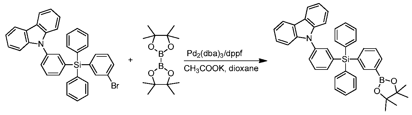
[0139] A suspension of 9H-carbazole (3.60 g, 21.53 mmol), bis(3-bromophenyl)diphenylsilane (21.28 g, 43.1 mmol), Pd2(dba)3 (0.394 g, 0.431 mmol), l,l'-Bis(diphenylphosphino)ferrocene (dppf, 0.394 g, 0.431 mmol) and sodium tert-butoxide (4.14 g, 43.1 mmol) in xylene (150 mL) was refluxed under nitrogen overnight. After cooling to room temperature, the organic solution was isolated by filtration. Upon evaporation of the solvent, the crude product was purified by column chromatography on silica gel with hexane:EtOAc (9:1, v/v) as eluent to yield 9-(3-((3- bromophenyl)diphenylsilyl)phenyl)-9H-carbazole (6.1 g, 49%) as white solid
Figure imgf000068_0003
[0140] A solution of 9-(3-((3-bromophenyl)diphenylsilyl)phenyl)-9H-carbazole (6.00 g, 10.33 mmol), 4,4,4',4',5,5,5',5'-octamethyl-2,2'-bi(l,3,2-dioxaborolane) (3.15 g, 12.40 mmol), potassium acetate (1.014 g, 10.33 mmol), Pd2(dba)3 (9.46 g, 10.33 mmol) and dppf (6.31 g, 10.33 mmol) in dioxane (200 mL) was refluxed under nitrogen overnight. After cooling to room temperature, the black reaction mixture was diluted with water, extracted with EtOAc and dried over Na2S04. Upon evaporation of the solvent, the crude product was purified by column chromatography on silica gel with hexane:EtOAc (9: 1, v/v) as eluent to yield 9-(3-(diphenyl(3- (4,4,5,5-tetramethyl-l,3,2-dioxaborolan-2-yl)phenyl)silyl)phenyl)-9H-carbazole (3.26 g, 50%) as a white solid.
Figure imgf000069_0001
[0141] A solution of 9-(3-(diphenyl(3-(4,4,5,5-tetramethyl-l,3,2-dioxaborolan-2- yl)phenyl)silyl)phenyl)-9H-carbazole (3.25 g, 5.18 mmol), 2-iododibenzo[£,<i]furan (1.523 g, 5.18 mmol), K2C03 (1.431 g, 10.36 mmol) and Pd(PPh3)4 (0.096 g, 0.083 mmol) in toluene (100 mL) and water (5 mL) was refluxed under nitrogen overnight. After cooling to room
temperature, the organic phase was isolated. Upon evaporation of the solvent, the residue was purified by column chromatography on silica with hexane:DCM (7:3, v/v) as eluent to yield Compound 34 (2.55 g, 74%) as a white solid. [0142] Example 13: Synthesis of Compound 35
Figure imgf000069_0002
[0143] Into a solution of 1 ,4-dibromobenzene (34 g, 144 mmol) in diethyl ether (600 mL) was added 2.5 butyllithium solution in hexane (60.3 mL, 151 mmol) dropwise at -78 °C. The solution was stirred at -78 °C for 3.5 hours before dichlorodiphenylsilane (13.49 mL, 65.5 mmol) dissolved in 20ml of diethyl ether was added dropwise. The reaction mixture was allowed to warm up to room temperature overnight and was quenched with water. The organic phase was isolated, filtered to remove solids, and dried over Na2S04. After evaporation of the solvent, the residue was purified by column chromatography on silica gel with hexane :toluene as eluent and precipitation from toluene to methanol to yield bis(4-bromophenyl)diphenylsilane (12 g, 37%) as a white powder.
Figure imgf000070_0001
[0144] A mixture solution of dibenzo[£,<i]thiophen-4-ylboronic acid (2.5 g, 10.96 mmol), bis(4-bromophenyl)diphenylsilane (11.92 g, 24.11 mmol), Pd(PPh3)4 (0.253 g, 0.219 mmol), and K2C03 (9.09 g, 65.8 mmol) in toluene (90 mL) and water (30 mL) was stirred at 90 °C under nitrogen overnight. After cooling to room temperature, the organic phase was isolated, and the aqueous phase was extracted with toluene. The combined organic solution was dried over Na2S04. Upon evaporation of the solvent, the residue was purified by column chromatography on silica gel with hexane:DCM(9/l, v/v) as eluent to yield (4-bromophenyl)(4-(dibenzo[£,<i] thiophen-4-yl)phenyl)diphenylsilane (5.2 g, 79%) as a white powder.
Figure imgf000070_0002
[0145] A suspension of (4-bromophenyl)(4-(dibenzo[¾,<i]thiophen-4-yl)phenyl)diphenylsilane (2.83 g, 4.74 mmol), 9H-3,9*-bicarbazole (1.731 g, 5.21 mmol), Pd2(dba)3 (0.087 g, 0.095 mmol), SPhos (0.078 g, 0.189 mmol), and sodium tert-butoxide (0.910 g, 9.47 mmol) in xylene (50 mL) was refluxed at 140 °C overnight. After cooling to room temperature, it was passed through a short plug of Celite, washed with toluene and DCM. The combined solution was evaporated, and the residue was purified by column chromatography on silica gel with hexane:DCM(7.5:2.5, v/v) as eluent to yield Compound 35 (3.76 g, 94%) as a white powder.
[0146] Example 14: Synthesis of Compound 36
Figure imgf000071_0001
[0147] A suspension of (4-bromophenyl)(4-(dibenzo[¾,(i]thiophen-4-yl)phenyl)diphenylsilane (2.83 g, 4.74 mmol), 9H-carbazole (0.808 g, 4.83 mmol), Pd2(dba)3 (0.087 g, 0.095 mmol), SPhos (0.078 g, 0.189 mmol), and sodium tert-butoxide (0.910 g, 9.47 mmol) in m-xylene (50 mL) was heated at 140 °C for 5 h. After cooling to room temperature, the solution was washed with aqueous ammonium chloride and water, dried over Na2S04, and passed through a short plug of Celite. Upon evaporation of the solvent, the residue was purified by column chromatography on silica gel with hexane:DCM (8:2, v/v) as eluent to yield Compound 36 (1.50 g, 46.3%) as a white powder. [0148] Example 15: Synthesis of Compound 37
Figure imgf000071_0002
[0149] A solution of dibenzo[£,<i]furan-4-ylboronic acid (2.60 g, 12.26 mmol), with bis(4- bromophenyl)diphenylsilane (12.12 g, 24.53 mmol), Pd(PPh3)4 (0.283 g, 0.245 mmol) and K2C03 (5.08 g, 36.8 mmol) in toluene (200 mL) and water (50 mL) was refluxed under nitrogen overnight. After cooling to room temperature, the organic phase was isolated. Upon evaporation of the solvent, the residue was purified by column chromatography on silica gel with
hexane:DCM (9:1, v/v) as eluent to yield (4-bromophenyl)(4-(dibenzo[£,<i]furan-4- yl)phenyl)diphenylsilane (3.14 g, 44%) as a white solid.
Figure imgf000071_0003
[0150] A suspension of (4-bromophenyl)(4-(dibenzo[¾,<i]furan-4-yl)phenyl)diphenylsilane
(3.15 g, 5.42 mmol), 9H-carbazole (0.996 g, 5.96 mmol), sodium tert-butoxide (1.041 g, 10.83 mmol) Pd2(dba)3 (0.099 g, 0.108 mmol) and dppf (0.066 g, 0.108 mmol) in xylene (150 mL) was refluxed under nitrogen for 24 h. A fter cooling to room temperature, the reaction mixture was filtered. Upon evaporation of the solvent, the residue was purified by column chromatography on silica with hexane:EtOAc (4: 1, v/v) as eluent to yield Compound 37 (3.4 g, 94%) as a white solid.
[0151] Example 16: Synthesis of Compound 38
Figure imgf000072_0001
[0152] A suspension of (3-bromophenyl)(3-(dibenzo[¾,<i]thiophen-2-yl)phenyl)diphenylsilane (3.81 g, 6.38 mmol), 9H-carbazole (1.173 g, 7.01 mmol), Pd2(dba)3 (0.117 g, 0.128 mmol), SPhos (0.105 g, 0.255 mmol), and sodium tert-butoxide (1.225 g, 12.75 mmol in xylene (200 mL) was refluxed under nitrogen overnight. After cooling to room temperature, the organic solution was isolated by filtration. Upon evaporation of the solvent, the residue was purified by column chromatography on silica gel with hexane:DCM (4:1 to 1 : 1, v/v) as eluent to yield Compound 38 (2.2 g, 50%>) as a white solid. [0153] Example 17: Synthesis of Compound 39
Figure imgf000072_0002
[0154] A mixture of (3-bromophenyl)(3-(dibenzo[^<i]furan-4-yl)phenyl)diphenylsilane (5.77 g, 9.92 mmol), 9-phenyl-9H,9*H-3,3*-bicarbazole (4.05 g, 9.92 mmol), Pd2(dba)3 (0.072 g, 0.079 mmol), SPhos (0.163 g, 0.397 mmol) and sodium tert-butoxide (1.430 g, 14.88 mmol) in xylene (220 mL) was refluxed under nitrogen overnight. After cooling to room temperature, the reaction was quenched with aqueous NH4C1 and extracted with EtOAc. The organic extracts were combined and dried with anhydrous MgSC^. After evaporating of the solvent, the residue was purified by column chromatography on silica gel with hexane:DCM (7/3 to 6/4, v/v) as eluent to yield the product (8.47 g, 94%) as a white solid.
[0155] Example 18: Synthesis of Compound 40
Figure imgf000073_0001
[0156] A solution of dibenzo[£,d]thiophen-4-ylboronic acid (7 g, 30.7 mmol), 1,2- dibromobenzene (7.43 ml, 61.4 mmol), Pd(PPh3)4 (0.709 g, 0.614 mmol), and K2C03 (12.73 g, 92 mmol) in toluene (250 mL) and water (40 mL) was stirred at 100 °C under nitrogen overnight. After cooling to room temperature, the organic phase was separated, washed with water and dried over Na2S04. Upon evaporation of the solvent, the residue was purified by column chromatography on silica gel with hexane:DCM (9.5/0.5, v/v) as eluent to yield 4-(2- bromophenyl)dibenzo[£,<i]thiophene (7.5g, 72%) as white crystals.
Figure imgf000073_0002
[0157] Into a solution of 4-(2-bromophenyl)dibenzo[£,<i]thiophene (3.5 g, 10.32 mmol) in ether (50 mL) was added n-butyl lithium (2.5 Mm hexane, 6.45 mL, 10.32 mmol) dropwise at - 78 °C. The solution was stirred at this temperature for 1 h to yield a 2-dibenzo[¾,d]thiophen-4- ylphenyl lithium. In another flask was prepared 3-bromophenyl lithium by addition of n-butyl lithium (2.5 Mm hexane, 6.45 mL, 10.32 mmol) into a solution of 1,3 -dibromobenzene (1.248 ml, 10.32 mmol) in ether (50 ml) at -78 °C. It was stirred at this temperature for 3.5 hours before transferring dropwise into a solution of dichlorodiphenylsilane (2.124 ml, 10.32 mmol) in ether (50.0 mL) at -78 °C. It was stirred at -78 °C for 2 hours and the 2-dibenzo[^ ]thiophen-4- ylphenyl lithium solution prepared above was slowly transferred to this solution at -78 °C. The reaction mixture was allowed to gradually warm to room temperature and stirred overnight. After quenching with water, the organic phase was isolated, dried over Na2S04. Upon evaporation of the solvent, the residue was purified by column chromatography on silica gel with hexane:DCM (9.5:0.5 to 9:1, v/v) as eluent to yield (3-bromophenyl)(2-(dibenzo[£,d]thiophen-4- yl)phenyl)diphenylsilane (3.5g, 56.8%) as a white solid.
Figure imgf000074_0001
[0158] A mixture of (3-bromophenyl)(2-(dibenzo[^<i]thiophen-4-yl)phenyl)diphenylsilane (3.5 g, 5.86 mmol), 9H-carbazole (0.979 g, 5.86 mmol), Pd2(dba)3 (0.107 g, 0.117 mmol), SPhos (0.096 g, 0.234 mmol), and sodium tert-butoxide (1.126 g, 11.71 mmol) in xylene (50 mL) was refluxed at 140 °C overnight. After cooling to room temperature, it was passed through a plug of Celite®. Upon evaporation off the solvent, the residue was purified by column chromatography on silica gel with hexane:DCM (9: 1) as eluent to yield Compound 40 (3 g, 74.9%) as a white solid.
[0159] Example 19: Synthesis of Compound 41
Figure imgf000074_0002
[0160] A mixture of (3-bromophenyl)(3-(dibenzo[£, ]furan-4-yl)phenyl)diphenylsilane (3 g, 5.16 mmol), 5H-benzofuro[3,2-c]carbazole (1.327 g, 5.16 mmol), Pd2(dba)3 (0.094 g, 0.103 mmol), SPhos (0.085 g, 0.206 mmol) and sodium tert-butoxide (1.487 g, 15.48 mmol) in m- xylene (100 mL) was stirred under nitrogen at 145 °C overnight. After cooling to room temperature, it was filtered through a short plug of Celite®. Upon evaporation of the solvent, the residue was purified by column chromatography on silica gel with hexane:dichloromethane (85/15, v/v) as eluent to yield Compound 41 (3.4g, 87%>) as a white solid.
[0161] Example 20: Synthesis of Compound 42
Figure imgf000075_0001
[0162] A solution of l-chlorobenzo[ 5]thieno[2, J-c]pyridine (1.136 g, 5.17 mmol), 9-(3- (diphenyl(3-(4,4,5,5-tetramethyl-l,3,2-dioxaborolan-2-yl)phenyl)silyl)phenyl)-9H-carbazole (2.95 g, 4.70 mmol), Pd(PPh3)4 (0.136 g, 0.118 mmol) and sodium carbonate (1.245 g, 11.75 mmol) inl,2-dimethoxyethane (50 mL) and water (8.50 mL) was heated at 110 °C under nitrogen overnight. The reaction mixture was purified by column chromatography on silica gel with hexane/EtOAc (8/2, v/v) as eluent to yield Compound 42 (2.9 g, 90%) as a yellowish white solid. [0163] Comparative Examples
[0164] Comparative Examples 1 : Synthesis of Comparative Compound CC-1
Figure imgf000075_0002
[0165] Into a solution of 9-(3-bromophenyl)-9H-carbazole (5 g, 15.52 mmol) in THF (50 mL) was added n-butyllithium (9.7 mL, 15.5 mmol, 1.6 M in hexane) dropwise at -78 °C, and the mixture was stirred for 2 h at -78 °C. In a separate flask, dichlorodiphenylsilane (1.5 mL, 7.1 mmol) was dissolved in 10 mL of THF and added dropwise to reaction mixture, which was then allowed to warm to room temperature overnight. Ethyl acetate (50 mL) and water (50 mL) were added and the layers separated. The aqueous layer was washed twice more with EtOAc and combined organics were washed with water and brine. Upon evaporation of the solvent, the residue was purified by column chromatography on silica gel with hexane:DCM (7/3, v/v) as eluent, recrystallization from hexane, and sublimation twice under vacuum (<10~5 Torr) to yield CC-1 (1.7 g) as white crystals.
[0166] Comparative Examples 2: Synthesis of Comparative Compound CC-2
Figure imgf000076_0001
[0167] A solution of 4-(3-bromophenyl)dibenzo[b,d]thiophene (7.15 g, 21.08 mmol), 9-(3- (4,4, 5,5-tetramethyl-l,3,2-dioxaborolan-2-yl)phenyl)-9H-carbazole (7.78 g, 21.08 mmol), SPhos (0.173 g, 0.422 mmol), Pd2(dba)3 (0.192 g, 0.211 mmol) and potassium phosphate monohydrate (9.71 g, 42.2 mmol) in toluene (200 mL) and water (10 mL) was refluxed under nitrogen overnight. After cooling to room temperature, the organic phase was isolated and evaporated to dryness. The residue was purified by column chromatography on silica gel with hexane:DCM (9 : 1 to 1 : 1 , v/v) as eluent, recrystallization from heptane, and sublimation under vacuum to yield CC-2 (6.4g, 61%) as white crystals.
[0168] It is understood that the various embodiments described herein are by way of example only, and are not intended to limit the scope of the invention. For example, many of the materials and structures described herein may be substituted with other materials and structures without deviating from the spirit of the invention. The present invention as claimed may therefore include variations from the particular examples and preferred embodiments described herein, as will be apparent to one of skill in the art. It is understood that various theories as to why the invention works are not intended to be limiting.

Claims

1. A compound of Formula I comprising:
Figure imgf000077_0001
Formula I,
wherein Ar and Ar' are independently selected from the group consisting of phenyl, biphenyl, napthyl, dibenzothiolyl, and dibenzofuranyl, which are optionally further substituted;
wherein Z is selected from Si and Ge;
wherein Li comprises aryl or heteroaryl groups, wherein any heteroatoms in the heteroaryl groups are nitrogen;
wherein L2 is a single bond or comprises aryl or heteroaryl groups, wherein any heteroatoms in the heteroaryl groups are nitrogen;
wherein Li and L2 are optionally further substituted;
wherein A contains a group selected from the group consisting of dibenzofuran, dibenzothiophene, azadibenzofuran, azadibenzothiophene, dibenzoselenophene and
azadibenzoselenophene, which are optionally further substituted, and wherein the substitution is optionally fused to at least one benzo ring; and
wherein B contains a group selected from the group consisting of carbazole and azacarbazole, which are optionally further substituted, and wherein the substitution is optionally fused to the carbazole or azacarbazole group.
2. The compound of claim 1, wherein A is selected from the group consisting of:
Figure imgf000078_0001
wherein B is selected from the group consisting of:
Figure imgf000079_0001
wherein Y1 and Y2 are independently selected from the group consisting of O, S, and Se;
wherein X1 to X10 are independently selected from the group consisting of CR and N, and wherein each benzo ring contains at most one N;
wherein R is selected from the group consisting of hydrogen, deuterium, halide, alkyl, cycloalkyl, heteroalkyl, arylalkyl, alkoxy, aryloxy, amino, silyl, alkenyl, cycloalkenyl, heteroalkenyl, alkynyl, aryl, heteroaryl, acyl, carbonyl, carboxylic acids, ester, nitrile, isonitrile, sulfanyl, sulfmyl, sulfonyl, phosphino, and combinations thereof.
Figure imgf000080_0001
4. The compound of claim 1 , wherein L2 is a single bond.
5. The compound of claim 1, wherein Li and L2 contain at least one phenyl bonded directly to Z.
6. The compound of claim 1 , wherein Ar and Ar' are phenyl.
7. The compound of claim 1, wherein Ar, Ar', A and B are independently substituted with at least one group selected from the group consisting of hydrogen, deuterium, halide, alkyl, cycloalkyl, heteroalkyl, arylalkyl, alkoxy, aryloxy, amino, silyl, alkenyl, cycloalkenyl, heteroalkenyl, alkynyl, aryl, heteroaryl, acyl, carbonyl, carboxylic acids, ester, nitrile, isonitrile, sulfanyl, sulfinyl, sulfonyl, phosphino, and combinations thereof.
8. The compound of claim 7, wherein aryl comprises phenyl, biphenyl, triphenyl, terphenyl, naphthalene, phenalene, phenanthrene, fluorene or chrysene; and wherein heteroaryl comprises dibenzothiophene, dibenzofuran, benzofuran, benzothiophene, pyrazole, imidazole, triazole, oxazole, thiazole, oxadiazole, oxatriazole, dioxazole, thiadiazole, pyridine, pyridazine, pyrimidine, pyrazine, triazine, indole, azaindole, benzimidazole, indazole, benzoxazole, benzisoxazole, benzothiazole, quinoline, isoquinoline, cinnoline, quinazoline, quinoxaline, naphthyridine, phthalazine, pteridine, xanthene, phenothiazine, phenoxazine, benzofuropyridine, furodipyridine, benzothienopyridine and thienodipyridine.
9. The compound of claim 1, wherein the compound is selected from the group consisting of
Figure imgf000081_0001
Figure imgf000082_0001
Figure imgf000083_0001
wherein Y1 and Y2 are independently selected from the group consisting of O, S and Se; and wherein Z is selected from the group consisting of Si and Ge.
10. The compound of claim 1, wherein the compound is selected from the group consisting of
Figure imgf000083_0002
Figure imgf000084_0001
Figure imgf000085_0001
Compound 37 Compound 38
Figure imgf000085_0002
11. A first device comprising an organic light emitting device, further comprising:
an anode;
a cathode; and
an organic layer, disposed between the anode and the cathode, comprising a compound having the Formula I:
Figure imgf000086_0001
Formula I,
wherein Ar and Ar' are independently selected from the group consisting of phenyl, biphenyl, napthyl, dibenzothiolyl, and dibenzofuranyl, which are optionally further substituted;
wherein Z is selected from Si and Ge;
wherein Li comprises aryl or heteroaryl groups, wherein any heteroatoms in the heteroaryl groups are nitrogen;
wherein L2 is a single bond or comprises aryl or heteroaryl groups, wherein any heteroatoms in the heteroaryl groups are nitrogen;
wherein Li and L2 are optionally further substituted;
wherein A contains a group selected from the group consisting of dibenzofuran, dibenzothiophene, azadibenzofuran, azadibenzothiophene, dibenzoselenophene and
azadibenzoselenophene, which are optionally further substituted, and wherein the substitution is optionally fused to at least one benzo ring; and
wherein B contains a group selected from the group consisting of carbazole and azacarbazole, which are optionally further substituted, and wherein the substitution is optionally fused to the carbazole or azacarbazole group.
12. The first device of claim 11, wherein the organic layer is an emissive layer and the compound of Formula I is a host.
13. The first device of claim 11, wherein the organic layer further comprises an emissive dopant.
Figure imgf000087_0001
85
Figure imgf000088_0001
wherein Ra, Rb, and Rc may represent mono, di, tri or tetra substitutions;
wherein Ra, Rb, and Rc are independently selected from the group consisting of hydrogen, deuterium, halide, alkyl, cycloalkyl, heteroalkyl, arylalkyl, alkoxy, aryloxy, amino, silyl, alkenyl, cycloalkenyl, heteroalkenyl, alkynyl, aryl, heteroaryl, acyl, carbonyl, carboxylic acids, ester, nitrile, isonitrile, sulfanyl, sulfinyl, sulfonyl, phosphino, and combinations thereof; and wherein two adjacent substituents of Ra, Rb, and Rc are optionally joined to form a fused ring. 15. The first device of claim 11, wherein the device further comprises a second organic layer that is a non-emissive layer and the compound having Formula I is a material in the second organic layer.
16. The first device of claim 11, wherein the organic layer is deposited using a solution process. 17. The first device of claim 15, wherein the second organic layer is a blocking layer and the compound having Formula I is a blocking material in the second organic layer.
18. The first device of claim 11 , wherein the first device is a consumer product.
The first device of claim 11 , wherein the first device is an organic lig emitting device.
PCT/US2012/039015 2011-05-25 2012-05-22 Host materials for oleds WO2012162325A1 (en)

Priority Applications (3)

Application Number Priority Date Filing Date Title
DE112012002237.8T DE112012002237B4 (en) 2011-05-25 2012-05-22 Host Materials for OLEDS
CN201280025504.8A CN103596963B (en) 2011-05-25 2012-05-22 Material of main part for organic light emitting apparatus
KR1020137031783A KR101922269B1 (en) 2011-05-25 2012-05-22 Host materials for oleds

Applications Claiming Priority (2)

Application Number Priority Date Filing Date Title
US13/067,345 US8748012B2 (en) 2011-05-25 2011-05-25 Host materials for OLED
US13/067,345 2011-05-25

Publications (1)

Publication Number Publication Date
WO2012162325A1 true WO2012162325A1 (en) 2012-11-29

Family

ID=46197712

Family Applications (1)

Application Number Title Priority Date Filing Date
PCT/US2012/039015 WO2012162325A1 (en) 2011-05-25 2012-05-22 Host materials for oleds

Country Status (6)

Country Link
US (1) US8748012B2 (en)
KR (1) KR101922269B1 (en)
CN (2) CN106831846B (en)
DE (1) DE112012002237B4 (en)
TW (2) TWI534244B (en)
WO (1) WO2012162325A1 (en)

Cited By (19)

* Cited by examiner, † Cited by third party
Publication number Priority date Publication date Assignee Title
CN103804409A (en) * 2014-02-19 2014-05-21 烟台万润精细化工股份有限公司 Silicon-containing organic electroluminescent material and application thereof as well as device manufactured by using same
WO2014157618A1 (en) 2013-03-29 2014-10-02 コニカミノルタ株式会社 Organic electroluminescent element, and lighting device and display device which are provided with same
WO2015000955A1 (en) 2013-07-02 2015-01-08 Basf Se Monosubstituted diazabenzimidazole carbene metal complexes for use in organic light emitting diodes
WO2015063046A1 (en) 2013-10-31 2015-05-07 Basf Se Azadibenzothiophenes for electronic applications
EP2993215A1 (en) 2014-09-04 2016-03-09 Idemitsu Kosan Co., Ltd. Azabenzimidazo[2,1-a]benzimidazoles for electronic applications
WO2016079667A1 (en) 2014-11-17 2016-05-26 Idemitsu Kosan Co., Ltd. Indole derivatives for electronic applications
EP3034506A1 (en) 2014-12-15 2016-06-22 Idemitsu Kosan Co., Ltd 4-functionalized carbazole derivatives for electronic applications
WO2016097983A1 (en) 2014-12-15 2016-06-23 Idemitsu Kosan Co., Ltd. 1-functionalized dibenzofurans and dibenzothiophenes for organic light emitting diodes (oleds)
EP3053918A1 (en) 2015-02-06 2016-08-10 Idemitsu Kosan Co., Ltd 2-carbazole substituted benzimidazoles for electronic applications
EP3054498A1 (en) 2015-02-06 2016-08-10 Idemitsu Kosan Co., Ltd. Bisimidazodiazocines
EP3061759A1 (en) 2015-02-24 2016-08-31 Idemitsu Kosan Co., Ltd Nitrile substituted dibenzofurans
EP3070144A1 (en) 2015-03-17 2016-09-21 Idemitsu Kosan Co., Ltd. Seven-membered ring compounds
EP3072943A1 (en) 2015-03-26 2016-09-28 Idemitsu Kosan Co., Ltd. Dibenzofuran/carbazole-substituted benzonitriles
EP3075737A1 (en) 2015-03-31 2016-10-05 Idemitsu Kosan Co., Ltd Benzimidazolo[1,2-a]benzimidazole carrying aryl- or heteroarylnitril groups for organic light emitting diodes
WO2016193243A1 (en) 2015-06-03 2016-12-08 Udc Ireland Limited Highly efficient oled devices with very short decay times
EP3239161A1 (en) 2013-07-31 2017-11-01 UDC Ireland Limited Luminescent diazabenzimidazole carbene metal complexes
US9862739B2 (en) 2014-03-31 2018-01-09 Udc Ireland Limited Metal complexes, comprising carbene ligands having an O-substituted non-cyclometalated aryl group and their use in organic light emitting diodes
US10199584B2 (en) 2016-08-10 2019-02-05 Samsung Electronics Co., Ltd. Organometallic compound and organic light-emitting device including the same
US10347851B2 (en) 2013-12-20 2019-07-09 Udc Ireland Limited Highly efficient OLED devices with very short decay times

Families Citing this family (23)

* Cited by examiner, † Cited by third party
Publication number Priority date Publication date Assignee Title
US8748012B2 (en) * 2011-05-25 2014-06-10 Universal Display Corporation Host materials for OLED
US9590189B2 (en) * 2011-07-13 2017-03-07 Youl Chon Chemical Co., Ltd. Host material for blue phosphor, and organic thin film and organic light-emitting device including same
KR101879716B1 (en) * 2011-07-20 2018-07-18 엘지디스플레이 주식회사 Phosphorescent host transporting material and Organic electroluminescent device using the same
US8652656B2 (en) * 2011-11-14 2014-02-18 Universal Display Corporation Triphenylene silane hosts
KR102253439B1 (en) * 2013-07-30 2021-05-20 삼성디스플레이 주식회사 Heterocyclic compound and organic light emitting device comprising same
KR102426713B1 (en) * 2014-09-01 2022-07-29 삼성디스플레이 주식회사 Amine-based compound and organic light emitting diode comprising the same
KR102503311B1 (en) * 2014-12-10 2023-02-28 롬엔드하스전자재료코리아유한회사 Organic Electroluminescent Compound and Organic Electroluminescent Device Comprising the Same
US9780316B2 (en) 2015-03-16 2017-10-03 Universal Display Corporation Organic electroluminescent materials and devices
US10651392B2 (en) 2015-09-30 2020-05-12 Samsung Electronics Co., Ltd. Organic light-emitting device
CN105384764B (en) * 2015-11-06 2017-12-15 山东盛华新材料科技股份有限公司 A kind of Organic charge transport material shown available for OLED and preparation method thereof
CN105418667B (en) * 2015-11-06 2018-03-13 山东盛华新材料科技股份有限公司 A kind of derivative of silicon tetraphenyl and dibenzothiophenes and preparation method thereof
CN105418665B (en) * 2015-11-06 2017-11-03 山东盛华新材料科技股份有限公司 A kind of Organic charge transport material and preparation method thereof
CN105418666B (en) * 2015-11-06 2018-03-06 山东盛华新材料科技股份有限公司 A kind of derivative of alkoxy dibenzothiophenes based on silicon tetraphenyl substitution and preparation method thereof
CN105367595B (en) * 2015-11-06 2017-12-26 山东盛华新材料科技股份有限公司 A kind of electroluminescent hole mobile material and preparation method thereof
CN105368445B (en) * 2015-11-06 2017-06-27 山东盛华新材料科技股份有限公司 A kind of electroluminescent organic material and preparation method thereof
KR101971485B1 (en) * 2015-12-14 2019-04-24 중앙대학교 산학협력단 Dendrimer composition having germanium core, organic optoelectronic device including the same
US10573819B2 (en) * 2016-04-01 2020-02-25 Duk San Neolux Co., Ltd. Compound for organic electronic element, organic electronic element comprising the same, and electronic device thereof
US10942912B1 (en) 2016-06-24 2021-03-09 Amazon Technologies, Inc. Chain logging using key-value data storage
CN108424420B (en) * 2017-09-30 2021-01-12 北京绿人科技有限责任公司 Triazine compound containing silicon atom, application thereof and organic electroluminescent device
KR20200014085A (en) * 2018-07-31 2020-02-10 삼성전자주식회사 Condensed cyclic compound and organic light emitting device including the same
US10860457B1 (en) 2019-02-15 2020-12-08 Amazon Technologies, Inc. Globally ordered event stream logging
US11758807B2 (en) * 2019-02-22 2023-09-12 Universal Display Corporation Organic electroluminescent materials and devices
KR102556018B1 (en) * 2020-05-19 2023-07-17 삼성디스플레이 주식회사 Heterocyclic compound, light emitting device comprising the same and electronic apparatus comprising the light emitting device

Citations (19)

* Cited by examiner, † Cited by third party
Publication number Priority date Publication date Assignee Title
US4769292A (en) 1987-03-02 1988-09-06 Eastman Kodak Company Electroluminescent device with modified thin film luminescent zone
US5247190A (en) 1989-04-20 1993-09-21 Cambridge Research And Innovation Limited Electroluminescent devices
US5703436A (en) 1994-12-13 1997-12-30 The Trustees Of Princeton University Transparent contacts for organic devices
US5707745A (en) 1994-12-13 1998-01-13 The Trustees Of Princeton University Multicolor organic light emitting devices
US5834893A (en) 1996-12-23 1998-11-10 The Trustees Of Princeton University High efficiency organic light emitting devices with light directing structures
US5844363A (en) 1997-01-23 1998-12-01 The Trustees Of Princeton Univ. Vacuum deposited, non-polymeric flexible organic light emitting devices
US6013982A (en) 1996-12-23 2000-01-11 The Trustees Of Princeton University Multicolor display devices
US6087196A (en) 1998-01-30 2000-07-11 The Trustees Of Princeton University Fabrication of organic semiconductor devices using ink jet printing
US6091195A (en) 1997-02-03 2000-07-18 The Trustees Of Princeton University Displays having mesa pixel configuration
US6097147A (en) 1998-09-14 2000-08-01 The Trustees Of Princeton University Structure for high efficiency electroluminescent device
US6294398B1 (en) 1999-11-23 2001-09-25 The Trustees Of Princeton University Method for patterning devices
US6303238B1 (en) 1997-12-01 2001-10-16 The Trustees Of Princeton University OLEDs doped with phosphorescent compounds
US6337102B1 (en) 1997-11-17 2002-01-08 The Trustees Of Princeton University Low pressure vapor phase deposition of organic thin films
US20030230980A1 (en) 2002-06-18 2003-12-18 Forrest Stephen R Very low voltage, high efficiency phosphorescent oled in a p-i-n structure
US20040174116A1 (en) 2001-08-20 2004-09-09 Lu Min-Hao Michael Transparent electrodes
US7279704B2 (en) 2004-05-18 2007-10-09 The University Of Southern California Complexes with tridentate ligands
EP2034538A1 (en) * 2006-06-02 2009-03-11 Idemitsu Kosan Co., Ltd. Material for organic electroluminescence element, and organic electroluminescence element using the material
US20100051914A1 (en) * 2008-09-03 2010-03-04 Samsung Mobile Display Co., Ltd. Silicon-containing compound and organic electroluminescent device employing the same
WO2011125680A1 (en) * 2010-03-31 2011-10-13 出光興産株式会社 Material for organic electroluminescent element, and organic electroluminescent element using same

Family Cites Families (102)

* Cited by examiner, † Cited by third party
Publication number Priority date Publication date Assignee Title
US5061569A (en) 1990-07-26 1991-10-29 Eastman Kodak Company Electroluminescent device with organic electroluminescent medium
EP0650955B1 (en) 1993-11-01 1998-08-19 Hodogaya Chemical Co., Ltd. Amine compound and electro-luminescence device comprising same
US6939625B2 (en) 1996-06-25 2005-09-06 Nôrthwestern University Organic light-emitting diodes and methods for assembly and enhanced charge injection
US6528187B1 (en) 1998-09-08 2003-03-04 Fuji Photo Film Co., Ltd. Material for luminescence element and luminescence element using the same
US6830828B2 (en) 1998-09-14 2004-12-14 The Trustees Of Princeton University Organometallic complexes as phosphorescent emitters in organic LEDs
US6458475B1 (en) 1999-11-24 2002-10-01 The Trustee Of Princeton University Organic light emitting diode having a blue phosphorescent molecule as an emitter
KR100377321B1 (en) 1999-12-31 2003-03-26 주식회사 엘지화학 Electronic device comprising organic compound having p-type semiconducting characteristics
US20020121638A1 (en) 2000-06-30 2002-09-05 Vladimir Grushin Electroluminescent iridium compounds with fluorinated phenylpyridines, phenylpyrimidines, and phenylquinolines and devices made with such compounds
EP1325671B1 (en) 2000-08-11 2012-10-24 The Trustees Of Princeton University Organometallic compounds and emission-shifting organic electrophosphorescence
US6579630B2 (en) 2000-12-07 2003-06-17 Canon Kabushiki Kaisha Deuterated semiconducting organic compounds used for opto-electronic devices
JP3812730B2 (en) 2001-02-01 2006-08-23 富士写真フイルム株式会社 Transition metal complex and light emitting device
JP4307000B2 (en) 2001-03-08 2009-08-05 キヤノン株式会社 Metal coordination compound, electroluminescent element and display device
JP4310077B2 (en) 2001-06-19 2009-08-05 キヤノン株式会社 Metal coordination compound and organic light emitting device
AU2002345362A1 (en) 2001-06-20 2003-01-08 Showa Denko K.K. Light emitting material and organic light-emitting device
US7250226B2 (en) 2001-08-31 2007-07-31 Nippon Hoso Kyokai Phosphorescent compound, a phosphorescent composition and an organic light-emitting device
US7431968B1 (en) 2001-09-04 2008-10-07 The Trustees Of Princeton University Process and apparatus for organic vapor jet deposition
US6835469B2 (en) 2001-10-17 2004-12-28 The University Of Southern California Phosphorescent compounds and devices comprising the same
US7166368B2 (en) 2001-11-07 2007-01-23 E. I. Du Pont De Nemours And Company Electroluminescent platinum compounds and devices made with such compounds
US6863997B2 (en) 2001-12-28 2005-03-08 The Trustees Of Princeton University White light emitting OLEDs from combined monomer and aggregate emission
KR100691543B1 (en) 2002-01-18 2007-03-09 주식회사 엘지화학 New material for transporting electron and organic electroluminescent display using the same
US7189989B2 (en) 2002-08-22 2007-03-13 Fuji Photo Film Co., Ltd. Light emitting element
WO2004020549A1 (en) 2002-08-27 2004-03-11 Fujitsu Limited Organometallic complexes, organic el devices, and organic el displays
US6687266B1 (en) 2002-11-08 2004-02-03 Universal Display Corporation Organic light emitting materials and devices
JP4365196B2 (en) 2002-12-27 2009-11-18 富士フイルム株式会社 Organic electroluminescence device
JP4365199B2 (en) 2002-12-27 2009-11-18 富士フイルム株式会社 Organic electroluminescence device
TWI347350B (en) 2003-03-24 2011-08-21 Univ Southern California Phenyl and fluorenyl substituted phenyl-pyrazole complexes of ir
US7090928B2 (en) 2003-04-01 2006-08-15 The University Of Southern California Binuclear compounds
EP2281861A3 (en) 2003-04-15 2012-03-28 Merck Patent GmbH Mixture of organic emission-enabled semiconductors and matrix materials, use of same and electronic components containing same
US7029765B2 (en) 2003-04-22 2006-04-18 Universal Display Corporation Organic light emitting devices having reduced pixel shrinkage
CN100483779C (en) 2003-05-29 2009-04-29 新日铁化学株式会社 Organic electroluminescent element
JP2005011610A (en) 2003-06-18 2005-01-13 Nippon Steel Chem Co Ltd Organic electroluminescent element
US20050025993A1 (en) 2003-07-25 2005-02-03 Thompson Mark E. Materials and structures for enhancing the performance of organic light emitting devices
TWI390006B (en) 2003-08-07 2013-03-21 Nippon Steel Chemical Co Organic EL materials with aluminum clamps
DE10338550A1 (en) 2003-08-19 2005-03-31 Basf Ag Transition metal complexes with carbene ligands as emitters for organic light-emitting diodes (OLEDs)
HU0302888D0 (en) 2003-09-09 2003-11-28 Pribenszky Csaba Dr In creasing of efficacity of stable storage by freezing of embryos in preimplantation stage with pretreatment by pressure
US20060269780A1 (en) 2003-09-25 2006-11-30 Takayuki Fukumatsu Organic electroluminescent device
JP4822687B2 (en) 2003-11-21 2011-11-24 富士フイルム株式会社 Organic electroluminescence device
US7332232B2 (en) 2004-02-03 2008-02-19 Universal Display Corporation OLEDs utilizing multidentate ligand systems
WO2005089024A1 (en) 2004-03-11 2005-09-22 Mitsubishi Chemical Corporation Composition for charge-transporting film and ion compound, charge-transporting film and organic electroluminescent device using same, and method for manufacturing organic electroluminescent device and method for producing charge-transporting film
TW200531592A (en) 2004-03-15 2005-09-16 Nippon Steel Chemical Co Organic electroluminescent device
JP4869565B2 (en) 2004-04-23 2012-02-08 富士フイルム株式会社 Organic electroluminescence device
US7445855B2 (en) 2004-05-18 2008-11-04 The University Of Southern California Cationic metal-carbene complexes
US7491823B2 (en) 2004-05-18 2009-02-17 The University Of Southern California Luminescent compounds with carbene ligands
US7534505B2 (en) 2004-05-18 2009-05-19 The University Of Southern California Organometallic compounds for use in electroluminescent devices
US7154114B2 (en) 2004-05-18 2006-12-26 Universal Display Corporation Cyclometallated iridium carbene complexes for use as hosts
US7393599B2 (en) 2004-05-18 2008-07-01 The University Of Southern California Luminescent compounds with carbene ligands
WO2005123873A1 (en) 2004-06-17 2005-12-29 Konica Minolta Holdings, Inc. Organic electroluminescent device material, organic electroluminescent device, display and illuminating device
CA2568667A1 (en) 2004-06-28 2006-01-05 Ciba Specialty Chemicals Holding Inc. Electroluminescent metal complexes with triazoles and benzotriazoles
US20060008670A1 (en) 2004-07-06 2006-01-12 Chun Lin Organic light emitting materials and devices
EP2271183B1 (en) 2004-07-23 2015-03-18 Konica Minolta Holdings, Inc. Organic electroluminescent element, display and illuminator
DE102004057072A1 (en) 2004-11-25 2006-06-01 Basf Ag Use of Transition Metal Carbene Complexes in Organic Light Emitting Diodes (OLEDs)
US7230107B1 (en) 2004-12-29 2007-06-12 E. I. Du Pont De Nemours And Company Metal quinoline complexes
US8362463B2 (en) 2004-12-30 2013-01-29 E. I. Du Pont De Nemours And Company Organometallic complexes
GB2437453B (en) 2005-02-04 2011-05-04 Konica Minolta Holdings Inc Material for organic electroluminescence element, organic electroluminescence element, display device and lighting device
KR100803125B1 (en) 2005-03-08 2008-02-14 엘지전자 주식회사 Red phosphorescent compounds and organic electroluminescence devices using the same
JP5125502B2 (en) 2005-03-16 2013-01-23 コニカミノルタホールディングス株式会社 Organic electroluminescence element material, organic electroluminescence element
JPWO2006103874A1 (en) 2005-03-29 2008-09-04 コニカミノルタホールディングス株式会社 ORGANIC ELECTROLUMINESCENT ELEMENT MATERIAL, ORGANIC ELECTROLUMINESCENT ELEMENT, DISPLAY DEVICE AND LIGHTING DEVICE
US7807275B2 (en) 2005-04-21 2010-10-05 Universal Display Corporation Non-blocked phosphorescent OLEDs
JP4533796B2 (en) 2005-05-06 2010-09-01 富士フイルム株式会社 Organic electroluminescence device
US9051344B2 (en) 2005-05-06 2015-06-09 Universal Display Corporation Stability OLED materials and devices
CN103435436A (en) 2005-05-31 2013-12-11 通用显示公司 Triphenylene hosts in phosphorescent light emitting diodes
US7638072B2 (en) 2005-06-27 2009-12-29 E. I. Du Pont De Nemours And Company Electrically conductive polymer compositions
JP5076891B2 (en) 2005-07-01 2012-11-21 コニカミノルタホールディングス株式会社 ORGANIC ELECTROLUMINESCENT ELEMENT MATERIAL, ORGANIC ELECTROLUMINESCENT ELEMENT, DISPLAY DEVICE AND LIGHTING DEVICE
WO2007028417A1 (en) 2005-09-07 2007-03-15 Technische Universität Braunschweig Triplett emitter having condensed five-membered rings
JP4887731B2 (en) 2005-10-26 2012-02-29 コニカミノルタホールディングス株式会社 Organic electroluminescence element, display device and lighting device
KR102103062B1 (en) 2006-02-10 2020-04-22 유니버셜 디스플레이 코포레이션 METAL COMPLEXES OF CYCLOMETALLATED IMIDAZO[1,2-f]PHENANTHRIDINE AND DIIMIDAZO[1,2-A:1',2'-C]QUINAZOLINE LIGANDS AND ISOELECTRONIC AND BENZANNULATED ANALOGS THEREOF
JP4823730B2 (en) 2006-03-20 2011-11-24 新日鐵化学株式会社 Luminescent layer compound and organic electroluminescent device
JP5186365B2 (en) 2006-04-26 2013-04-17 出光興産株式会社 Aromatic amine derivatives and organic electroluminescence devices using them
US8076839B2 (en) 2006-05-11 2011-12-13 Idemitsu Kosan Co., Ltd. Organic electroluminescence device
CN101506192A (en) 2006-08-23 2009-08-12 出光兴产株式会社 Aromatic amine derivative and organic electroluminescent element using same
JP5589251B2 (en) 2006-09-21 2014-09-17 コニカミノルタ株式会社 Organic electroluminescence element material
JP5133259B2 (en) 2006-11-24 2013-01-30 出光興産株式会社 Aromatic amine derivative and organic electroluminescence device using the same
US8119255B2 (en) 2006-12-08 2012-02-21 Universal Display Corporation Cross-linkable iridium complexes and organic light-emitting devices using the same
KR101532798B1 (en) 2007-02-23 2015-06-30 바스프 에스이 Electroluminescent metal complexes with benzotriazoles
JP5638246B2 (en) 2007-03-08 2014-12-10 ユニバーサル ディスプレイ コーポレイション Phosphorescent material
US7989091B2 (en) 2007-04-26 2011-08-02 Basf Se Silanes containing phenothiazine-S-oxide or phenothiazine-S,S-dioxide groups and the use thereof in OLEDs
WO2008156879A1 (en) 2007-06-20 2008-12-24 Universal Display Corporation Blue phosphorescent imidazophenanthridine materials
EP2170911B1 (en) 2007-06-22 2018-11-28 UDC Ireland Limited Light emitting cu(i) complexes
TW200909560A (en) 2007-07-07 2009-03-01 Idemitsu Kosan Co Organic electroluminescence device and material for organic electroluminescence devcie
KR20100031723A (en) 2007-07-07 2010-03-24 이데미쓰 고산 가부시키가이샤 Chrysene derivative and organic electroluminescent device using the same
US8779655B2 (en) 2007-07-07 2014-07-15 Idemitsu Kosan Co., Ltd. Organic electroluminescence device and material for organic electroluminescence device
WO2009008200A1 (en) 2007-07-07 2009-01-15 Idemitsu Kosan Co., Ltd. Naphthalene derivative, material for organic el element, and organic el element using the material
US20090045731A1 (en) 2007-07-07 2009-02-19 Idemitsu Kosan Co., Ltd. Organic electroluminescence device and material for organic electroluminescence device
TW200902675A (en) 2007-07-10 2009-01-16 Idemitsu Kosan Co Material for organic electroluminescence device and organic electroluminescence device utilizing the same
US8080658B2 (en) 2007-07-10 2011-12-20 Idemitsu Kosan Co., Ltd. Material for organic electroluminescent element and organic electroluminescent element employing the same
WO2009018009A1 (en) 2007-07-27 2009-02-05 E. I. Du Pont De Nemours And Company Aqueous dispersions of electrically conducting polymers containing inorganic nanoparticles
JP2009040728A (en) 2007-08-09 2009-02-26 Canon Inc Organometallic complex and organic light-emitting element using the same
US8728632B2 (en) 2007-10-17 2014-05-20 Basf Se Metal complexes comprising bridged carbene ligands and use thereof in OLEDs
US20090101870A1 (en) 2007-10-22 2009-04-23 E. I. Du Pont De Nemours And Company Electron transport bi-layers and devices made with such bi-layers
US7914908B2 (en) 2007-11-02 2011-03-29 Global Oled Technology Llc Organic electroluminescent device having an azatriphenylene derivative
CN101861291A (en) 2007-11-15 2010-10-13 出光兴产株式会社 Benzo derivatives and organic electroluminescent element using the same
US8574725B2 (en) 2007-11-22 2013-11-05 Idemitsu Kosan Co., Ltd. Organic el element and solution containing organic el material
WO2009073245A1 (en) 2007-12-06 2009-06-11 Universal Display Corporation Light-emitting organometallic complexes
WO2009085344A2 (en) 2007-12-28 2009-07-09 Universal Display Corporation Dibenzothiophene-containing materials in phosphorescent light emitting diodes
JP5709528B2 (en) 2008-02-12 2015-04-30 ビーエーエスエフ ソシエタス・ヨーロピアBasf Se Electroluminescent metal complex using dibenzo [f, h] quinoxaline
JP5536054B2 (en) 2008-06-30 2014-07-02 ユニバーサル・ディスプレイ・コーポレーション Hole transport material having sulfur-containing groups
KR20100028168A (en) * 2008-09-04 2010-03-12 다우어드밴스드디스플레이머티리얼 유한회사 Novel organic electroluminescent compounds and organic electroluminescent device using the same
US9034483B2 (en) 2008-09-16 2015-05-19 Universal Display Corporation Phosphorescent materials
CN102341403B (en) * 2009-01-07 2014-12-03 巴斯夫欧洲公司 Silyl- and heteroatom-substituted compounds selected from carbazoles, dibenzofurans, dibenzothiophenes and dibenzophospholes, and use thereof in organic electronics
WO2010079501A2 (en) 2009-01-12 2010-07-15 Hanumanth Raju Chandra Chari A linear electric generator which generates electricity by the up and down movement of the rotor. the amount of energy put in to move the rotor up is generated back when the rotor moves down
JP5939984B2 (en) 2009-10-28 2016-06-29 ビーエーエスエフ ソシエタス・ヨーロピアBasf Se Heteroleptic carbene complexes and uses thereof in organic electronics
US8748012B2 (en) * 2011-05-25 2014-06-10 Universal Display Corporation Host materials for OLED

Patent Citations (20)

* Cited by examiner, † Cited by third party
Publication number Priority date Publication date Assignee Title
US4769292A (en) 1987-03-02 1988-09-06 Eastman Kodak Company Electroluminescent device with modified thin film luminescent zone
US5247190A (en) 1989-04-20 1993-09-21 Cambridge Research And Innovation Limited Electroluminescent devices
US5703436A (en) 1994-12-13 1997-12-30 The Trustees Of Princeton University Transparent contacts for organic devices
US5707745A (en) 1994-12-13 1998-01-13 The Trustees Of Princeton University Multicolor organic light emitting devices
US5834893A (en) 1996-12-23 1998-11-10 The Trustees Of Princeton University High efficiency organic light emitting devices with light directing structures
US6013982A (en) 1996-12-23 2000-01-11 The Trustees Of Princeton University Multicolor display devices
US5844363A (en) 1997-01-23 1998-12-01 The Trustees Of Princeton Univ. Vacuum deposited, non-polymeric flexible organic light emitting devices
US6091195A (en) 1997-02-03 2000-07-18 The Trustees Of Princeton University Displays having mesa pixel configuration
US6337102B1 (en) 1997-11-17 2002-01-08 The Trustees Of Princeton University Low pressure vapor phase deposition of organic thin films
US6303238B1 (en) 1997-12-01 2001-10-16 The Trustees Of Princeton University OLEDs doped with phosphorescent compounds
US6087196A (en) 1998-01-30 2000-07-11 The Trustees Of Princeton University Fabrication of organic semiconductor devices using ink jet printing
US6097147A (en) 1998-09-14 2000-08-01 The Trustees Of Princeton University Structure for high efficiency electroluminescent device
US6294398B1 (en) 1999-11-23 2001-09-25 The Trustees Of Princeton University Method for patterning devices
US6468819B1 (en) 1999-11-23 2002-10-22 The Trustees Of Princeton University Method for patterning organic thin film devices using a die
US20040174116A1 (en) 2001-08-20 2004-09-09 Lu Min-Hao Michael Transparent electrodes
US20030230980A1 (en) 2002-06-18 2003-12-18 Forrest Stephen R Very low voltage, high efficiency phosphorescent oled in a p-i-n structure
US7279704B2 (en) 2004-05-18 2007-10-09 The University Of Southern California Complexes with tridentate ligands
EP2034538A1 (en) * 2006-06-02 2009-03-11 Idemitsu Kosan Co., Ltd. Material for organic electroluminescence element, and organic electroluminescence element using the material
US20100051914A1 (en) * 2008-09-03 2010-03-04 Samsung Mobile Display Co., Ltd. Silicon-containing compound and organic electroluminescent device employing the same
WO2011125680A1 (en) * 2010-03-31 2011-10-13 出光興産株式会社 Material for organic electroluminescent element, and organic electroluminescent element using same

Non-Patent Citations (2)

* Cited by examiner, † Cited by third party
Title
BALDO ET AL.: "Highly Efficient Phosphorescent Emission from Organic Electroluminescent Devices", NATURE, vol. 395, 1998, pages 151 - 154, XP001002103, DOI: doi:10.1038/25954
BALDO ET AL.: "Very high-efficiency green organic light-emitting devices based on electrophosphorescence", APPL. PHYS. LETT., vol. 75, no. 3, 1999, pages 4 - 6, XP012023409, DOI: doi:10.1063/1.124258

Cited By (32)

* Cited by examiner, † Cited by third party
Publication number Priority date Publication date Assignee Title
WO2014157618A1 (en) 2013-03-29 2014-10-02 コニカミノルタ株式会社 Organic electroluminescent element, and lighting device and display device which are provided with same
JP2014209618A (en) * 2013-03-29 2014-11-06 コニカミノルタ株式会社 Organic electroluminescent compound, organic electroluminescent element, and illuminating device and display device including the same
US10135002B2 (en) 2013-03-29 2018-11-20 Konica Minolta, Inc. Organic electroluminescent element, and lighting device and display device which are provided with same
WO2015000955A1 (en) 2013-07-02 2015-01-08 Basf Se Monosubstituted diazabenzimidazole carbene metal complexes for use in organic light emitting diodes
EP3608329A1 (en) 2013-07-02 2020-02-12 UDC Ireland Limited Monosubstituted diazabenzimidazole carbene metal complexes for use in organic light emitting diodes
EP3266789A1 (en) 2013-07-02 2018-01-10 UDC Ireland Limited Monosubstituted diazabenzimidazole carbene metal complexes for use in organic light emitting diodes
EP3239161A1 (en) 2013-07-31 2017-11-01 UDC Ireland Limited Luminescent diazabenzimidazole carbene metal complexes
WO2015063046A1 (en) 2013-10-31 2015-05-07 Basf Se Azadibenzothiophenes for electronic applications
US11765967B2 (en) 2013-12-20 2023-09-19 Udc Ireland Limited Highly efficient OLED devices with very short decay times
US10347851B2 (en) 2013-12-20 2019-07-09 Udc Ireland Limited Highly efficient OLED devices with very short decay times
US11075346B2 (en) 2013-12-20 2021-07-27 Udc Ireland Limited Highly efficient OLED devices with very short decay times
EP3916822A1 (en) 2013-12-20 2021-12-01 UDC Ireland Limited Highly efficient oled devices with very short decay times
CN103804409B (en) * 2014-02-19 2016-05-25 中节能万润股份有限公司 The device of a kind of siliceous electroluminescent organic material and application and its making
CN103804409A (en) * 2014-02-19 2014-05-21 烟台万润精细化工股份有限公司 Silicon-containing organic electroluminescent material and application thereof as well as device manufactured by using same
US10118939B2 (en) 2014-03-31 2018-11-06 Udc Ireland Limited Metal complexes, comprising carbene ligands having an o-substituted non-cyclometalated aryl group and their use in organic light emitting diodes
US9862739B2 (en) 2014-03-31 2018-01-09 Udc Ireland Limited Metal complexes, comprising carbene ligands having an O-substituted non-cyclometalated aryl group and their use in organic light emitting diodes
US10370396B2 (en) 2014-03-31 2019-08-06 Udc Ireland Limited Metal complexes, comprising carbene ligands having an O-substituted non-cyclometallated aryl group and their use in organic light emitting diodes
EP2993215A1 (en) 2014-09-04 2016-03-09 Idemitsu Kosan Co., Ltd. Azabenzimidazo[2,1-a]benzimidazoles for electronic applications
WO2016079667A1 (en) 2014-11-17 2016-05-26 Idemitsu Kosan Co., Ltd. Indole derivatives for electronic applications
WO2016097983A1 (en) 2014-12-15 2016-06-23 Idemitsu Kosan Co., Ltd. 1-functionalized dibenzofurans and dibenzothiophenes for organic light emitting diodes (oleds)
EP3034506A1 (en) 2014-12-15 2016-06-22 Idemitsu Kosan Co., Ltd 4-functionalized carbazole derivatives for electronic applications
WO2016125110A1 (en) 2015-02-06 2016-08-11 Idemitsu Kosan Co., Ltd. Bisimidazolodiazocines
EP3054498A1 (en) 2015-02-06 2016-08-10 Idemitsu Kosan Co., Ltd. Bisimidazodiazocines
EP3053918A1 (en) 2015-02-06 2016-08-10 Idemitsu Kosan Co., Ltd 2-carbazole substituted benzimidazoles for electronic applications
EP3061759A1 (en) 2015-02-24 2016-08-31 Idemitsu Kosan Co., Ltd Nitrile substituted dibenzofurans
EP3070144A1 (en) 2015-03-17 2016-09-21 Idemitsu Kosan Co., Ltd. Seven-membered ring compounds
EP3072943A1 (en) 2015-03-26 2016-09-28 Idemitsu Kosan Co., Ltd. Dibenzofuran/carbazole-substituted benzonitriles
EP3075737A1 (en) 2015-03-31 2016-10-05 Idemitsu Kosan Co., Ltd Benzimidazolo[1,2-a]benzimidazole carrying aryl- or heteroarylnitril groups for organic light emitting diodes
WO2016157113A1 (en) 2015-03-31 2016-10-06 Idemitsu Kosan Co., Ltd. Benzimidazolo[1,2-a]benzimidazole carrying aryl- or heteroarylnitril groups for organic light emitting diodes
WO2016193243A1 (en) 2015-06-03 2016-12-08 Udc Ireland Limited Highly efficient oled devices with very short decay times
EP4060757A1 (en) 2015-06-03 2022-09-21 UDC Ireland Limited Highly efficient oled devices with very short decay times
US10199584B2 (en) 2016-08-10 2019-02-05 Samsung Electronics Co., Ltd. Organometallic compound and organic light-emitting device including the same

Also Published As

Publication number Publication date
TWI580762B (en) 2017-05-01
DE112012002237T5 (en) 2014-04-30
KR20140029473A (en) 2014-03-10
KR101922269B1 (en) 2018-11-26
US20120298966A1 (en) 2012-11-29
TW201300505A (en) 2013-01-01
US8748012B2 (en) 2014-06-10
TW201623577A (en) 2016-07-01
CN103596963B (en) 2016-12-21
CN103596963A (en) 2014-02-19
CN106831846A (en) 2017-06-13
TWI534244B (en) 2016-05-21
CN106831846B (en) 2020-04-21
DE112012002237B4 (en) 2022-12-22

Similar Documents

Publication Publication Date Title
KR102091968B1 (en) Novel heteroleptic iridium complexes
KR102090896B1 (en) Triphenylene silane hosts
EP2551932B1 (en) Host materials for phosphorescent oleds
KR101922269B1 (en) Host materials for oleds
EP2826781B1 (en) Bicarbazole containing compounds for OLED
KR102084336B1 (en) Triphenylene-benzofuran/benzothiophene/benzoselenophene compounds with substituents joining to form fused rings
EP2694503B1 (en) Substituted oligoazacarbazoles for light emitting diodes
KR101843211B1 (en) Bicarbazole containing compounds for oleds
EP2594572B1 (en) Organic light emitting materials
US20150001471A1 (en) Novel host materials for pholeds
WO2012102967A1 (en) Aza - dibenzothiophene, aza - dibenzofuran and aza - dibenzoselenophene derivatives for use in oled &#39; s
WO2012148511A1 (en) 5-substituted 2-phenylquinoline complexes materials for light emitting diode
WO2011109042A1 (en) Phosphorescent materials
KR20130100330A (en) Novel 3, 9-linked oligocarbazole-based hosts, containing dbt and dbf fragments, separated by aromatic spacers
KR20150009461A (en) Donor-acceptor compounds with nitrogen containing heteropolyaromatics as the electron acceptor
KR20240051905A (en) Organic electroluminescent materials and devices

Legal Events

Date Code Title Description
121 Ep: the epo has been informed by wipo that ep was designated in this application

Ref document number: 12724818

Country of ref document: EP

Kind code of ref document: A1

WWE Wipo information: entry into national phase

Ref document number: 1120120022378

Country of ref document: DE

Ref document number: 112012002237

Country of ref document: DE

ENP Entry into the national phase

Ref document number: 20137031783

Country of ref document: KR

Kind code of ref document: A

122 Ep: pct application non-entry in european phase

Ref document number: 12724818

Country of ref document: EP

Kind code of ref document: A1