WO2012161128A1 - 荷電粒子線装置および静電チャック装置 - Google Patents
荷電粒子線装置および静電チャック装置 Download PDFInfo
- Publication number
- WO2012161128A1 WO2012161128A1 PCT/JP2012/062835 JP2012062835W WO2012161128A1 WO 2012161128 A1 WO2012161128 A1 WO 2012161128A1 JP 2012062835 W JP2012062835 W JP 2012062835W WO 2012161128 A1 WO2012161128 A1 WO 2012161128A1
- Authority
- WO
- WIPO (PCT)
- Prior art keywords
- electrostatic chuck
- sample
- voltage
- chuck
- wafer
- Prior art date
- Legal status (The legal status is an assumption and is not a legal conclusion. Google has not performed a legal analysis and makes no representation as to the accuracy of the status listed.)
- Ceased
Links
Images



Classifications
-
- H—ELECTRICITY
- H01—ELECTRIC ELEMENTS
- H01J—ELECTRIC DISCHARGE TUBES OR DISCHARGE LAMPS
- H01J37/00—Discharge tubes with provision for introducing objects or material to be exposed to the discharge, e.g. for the purpose of examination or processing thereof
- H01J37/02—Details
- H01J37/20—Means for supporting or positioning the object or the material; Means for adjusting diaphragms or lenses associated with the support
-
- H—ELECTRICITY
- H10—SEMICONDUCTOR DEVICES; ELECTRIC SOLID-STATE DEVICES NOT OTHERWISE PROVIDED FOR
- H10P—GENERIC PROCESSES OR APPARATUS FOR THE MANUFACTURE OR TREATMENT OF DEVICES COVERED BY CLASS H10
- H10P72/00—Handling or holding of wafers, substrates or devices during manufacture or treatment thereof
- H10P72/70—Handling or holding of wafers, substrates or devices during manufacture or treatment thereof for supporting or gripping
-
- B—PERFORMING OPERATIONS; TRANSPORTING
- B23—MACHINE TOOLS; METAL-WORKING NOT OTHERWISE PROVIDED FOR
- B23Q—DETAILS, COMPONENTS, OR ACCESSORIES FOR MACHINE TOOLS, e.g. ARRANGEMENTS FOR COPYING OR CONTROLLING; MACHINE TOOLS IN GENERAL CHARACTERISED BY THE CONSTRUCTION OF PARTICULAR DETAILS OR COMPONENTS; COMBINATIONS OR ASSOCIATIONS OF METAL-WORKING MACHINES, NOT DIRECTED TO A PARTICULAR RESULT
- B23Q3/00—Devices holding, supporting, or positioning work or tools, of a kind normally removable from the machine
- B23Q3/15—Devices for holding work using magnetic or electric force acting directly on the work
-
- H—ELECTRICITY
- H01—ELECTRIC ELEMENTS
- H01J—ELECTRIC DISCHARGE TUBES OR DISCHARGE LAMPS
- H01J37/00—Discharge tubes with provision for introducing objects or material to be exposed to the discharge, e.g. for the purpose of examination or processing thereof
- H01J37/26—Electron or ion microscopes; Electron or ion diffraction tubes
- H01J37/28—Electron or ion microscopes; Electron or ion diffraction tubes with scanning beams
-
- H—ELECTRICITY
- H02—GENERATION; CONVERSION OR DISTRIBUTION OF ELECTRIC POWER
- H02N—ELECTRIC MACHINES NOT OTHERWISE PROVIDED FOR
- H02N13/00—Clutches or holding devices using electrostatic attraction, e.g. using Johnson-Rahbek effect
-
- H—ELECTRICITY
- H10—SEMICONDUCTOR DEVICES; ELECTRIC SOLID-STATE DEVICES NOT OTHERWISE PROVIDED FOR
- H10P—GENERIC PROCESSES OR APPARATUS FOR THE MANUFACTURE OR TREATMENT OF DEVICES COVERED BY CLASS H10
- H10P72/00—Handling or holding of wafers, substrates or devices during manufacture or treatment thereof
- H10P72/70—Handling or holding of wafers, substrates or devices during manufacture or treatment thereof for supporting or gripping
- H10P72/72—Handling or holding of wafers, substrates or devices during manufacture or treatment thereof for supporting or gripping using electrostatic chucks
-
- H—ELECTRICITY
- H01—ELECTRIC ELEMENTS
- H01J—ELECTRIC DISCHARGE TUBES OR DISCHARGE LAMPS
- H01J2237/00—Discharge tubes exposing object to beam, e.g. for analysis treatment, etching, imaging
- H01J2237/20—Positioning, supporting, modifying or maintaining the physical state of objects being observed or treated
- H01J2237/2007—Holding mechanisms
-
- H—ELECTRICITY
- H01—ELECTRIC ELEMENTS
- H01J—ELECTRIC DISCHARGE TUBES OR DISCHARGE LAMPS
- H01J2237/00—Discharge tubes exposing object to beam, e.g. for analysis treatment, etching, imaging
- H01J2237/248—Components associated with the control of the tube
Definitions
- the present invention relates to a sample holding control technique in an electrostatic chuck of a charged particle beam apparatus.
- Devices for processing semiconductor wafers using charged particle beams, devices for inspecting circuit patterns on semiconductor wafers, etc. have a sample holding function using an electrostatic chuck method that uses electrostatic adsorption force to hold semiconductor wafers. have.
- An example of such an apparatus is an electron beam length measuring machine.
- this method the width and position of a circuit pattern formed on a semiconductor wafer are measured.
- electrostatic chuck methods There are two types of electrostatic chuck methods: the Coulomb method and the Johnson-Rahbek method, but the electron beam length measuring instrument employs the Coulomb method in which no current flows through the semiconductor wafer because the probe current is very small.
- the Coulomb method requires a larger applied voltage than the Johnson Labek method because the dielectric has a very high resistivity. For this reason, the problem described later occurs.
- the method for determining whether or not a semiconductor wafer (hereinafter referred to as “wafer” as appropriate) is normally attracted by the electrostatic chuck is as follows.
- a reference value a method has been proposed in which when the current is smaller than the reference value, it is determined that the wafer is not normally placed (abnormal) (see, for example, Patent Document 1).
- An electrostatic chuck may cause a phenomenon in which an attractive force remains as a residual attractive force even when the power is turned off due to the relationship between applied voltage and time. This is a state in which the charges induced on the wafer surface and the like are not relaxed and an unintended adsorption force remains. As the voltage applied to the electrostatic chuck increases, the residual attractive force tends to increase. In such a state, the sample chamber is opened to the atmosphere and manually taken out, and there is a problem that the downtime of the apparatus increases.
- the present invention has been made in view of such a background, and an object of the present invention is to improve the reliability of the apparatus by setting the applied voltage according to the situation.
- a charged particle beam apparatus of the present invention is a charged particle beam apparatus that generates an image of a sample by irradiating a sample held by an electrostatic chuck on a sample stage with an electron beam.
- it applies a preset initial voltage to the chuck electrode of the electrostatic chuck, determines whether or not the sample is normally attracted to the electrostatic chuck, and the sample is normally attracted to the electrostatic chuck. If it is determined that the sample is not, the electrostatic chuck controller is provided to increase the voltage applied to the chuck electrode until it is determined that the sample is normally attracted to the electrostatic chuck.
- Other solutions will be described as appropriate in the embodiments.
- FIG. 1 is a diagram illustrating a configuration of a charged particle beam apparatus 1 according to the embodiment.
- the charged particle beam apparatus 1 includes an electron optical system column 2, a sample chamber 3, and a control system.
- a wafer (sample) 24 is held on the sample stage 25 by an electrostatic chuck 30 having a chuck electrode 26.
- the Z sensor 27 detects the height of the wafer 24 and outputs the height information to the Z sensor control unit 11.
- a primary electron beam 16 is emitted from an electron gun 14 in the electron optical system column 2 by an extraction electrode 15.
- the primary electron beam 16 is focused by the focus coil 20 or the dynamic focus coil 21, deflected by the deflector 19, and scanned on the wafer 24.
- the blanking deflector 17 deflects the primary electron beam 16 so as not to pass through the diaphragm 18.
- the electron gun 14, the diaphragm 18 and the focus coil 20 are controlled by the electron optical control unit 8.
- the blanking deflector 17, the deflector 19, and the moving focus coil 21 are controlled by the deflection control unit 10.
- the image processing unit 9 When the wafer 24 is irradiated with the primary electron beam 16, reflected electrons and secondary electrons are generated, which are accelerated by the E ⁇ B deflector 23 and detected by the secondary electron detector 22.
- the backscattered electron and secondary electron detection signals detected by the secondary electron detector 22 are input to the image processing unit 9.
- the image processing unit 9 generates image data based on the control information, and the generated image data is displayed as an image on a display device (not shown) via the Ethernet (registered trademark) 6.
- the electro-optic control unit 8, the image processing unit 9, the deflection control unit 10, and the Z sensor control unit 11 are controlled by a host control CPU (Central Processing Unit) 5 via a VME_Bus (VERSA Module Eurocard_Bus) 7.
- the sample stage control unit 12 controls the position of the sample stage 25. Assuming that the plane perpendicular to the vertical axis is the XY plane, the sample stage 25 can move in the X direction and the Y direction, and the sample stage control unit 12 grasps the XY coordinates of the sample stage 25 and sets preset information. The sample stage 25 is moved based on the above.
- the electrostatic chuck control unit 13 applies a voltage to the chuck electrode 26 of the electrostatic chuck 30 and also determines the suction state of the wafer 24. In addition, the electrostatic chuck control unit 13 can change the voltage to be applied. Next, details of the electrostatic chuck controller 13 will be described.
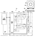
- FIG. 2 is a diagram illustrating a configuration of the electrostatic chuck control unit 13.
- the electrostatic chuck control unit 13 includes an applied voltage unit 131, a current detection unit 132, an adsorption determination unit 133, an output voltage partial pressure monitor unit 134, and a control IC (Integrated Circuit) 135. It is equipped with.
- the chuck electrode 26 is embedded in the sample stage 25 and constitutes a concentric dipole type electrostatic chuck 30.
- the applied voltage unit 131 applies a voltage to the chuck electrode 26 of the electrostatic chuck 30. Note that the potential of the portion indicated by the alternate long and short dash line is, for example, the potential VR.
- the applied voltage unit 131 is configured on this potential VR. For this reason, in the output part of the applied voltage part 131, electric potential VR is added from GND (ground) of the charged particle beam apparatus 1, and becomes high electric potential.
- the applied voltage unit 131 has an output voltage variable function (not shown), and the host control IC 137 controls the voltage applied to the chuck electrode 26 via the control IC 135.
- the voltage applied to the chuck electrode 26 can be set or turned ON / OFF from the outside.
- the +/ ⁇ electrode area ratio of the chuck electrode 26 is applied to the + electrode and the ⁇ electrode. It is sufficient to give a slight voltage difference to the voltage to be applied.
- the control IC 135 detects the transient current generated from the chuck electrode 26 by the current detection unit 132, and compares the magnitude of the transient current with a preset threshold value by the adsorption determination unit 133. Can be recognized.
- the output voltage division monitor unit 134 is for monitoring the actual applied voltage (hereinafter referred to as “chuck voltage” as appropriate) to the chuck electrode 26, and the chuck voltage is obtained from an ADC (Analog to Digital Converter) 136. Via the host control IC 137.
- ADC Analog to Digital Converter
- the electrostatic chuck control unit 13 can change the voltage applied to the chuck electrode 26 according to the situation of the wafer 24.
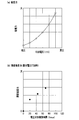
- FIG. 3A is a graph showing the relationship between the magnitude of the voltage applied to the chuck electrode 26 and the attracting force of the wafer 24. As shown in this graph, it can be seen that the greater the applied voltage of the chuck electrode 26, the greater the attractive force of the wafer 24. If the adsorption force is large, a problem of generation of foreign matters due to friction occurs, and therefore the voltage should not be higher than necessary.
- FIG. 3B is a graph showing the relationship between the voltage application integration time and the residual adsorption force when the maximum voltage is applied to the chuck electrode 26. As shown in this graph, it can be seen that the longer the time during which the voltage is applied to the chuck electrode 26, the greater the residual attractive force. It has also been found that the greater the attractive force (the greater the applied voltage), the greater the residual attractive force. Therefore, in order to suppress the influence of the residual adsorption force, it is required to reduce the applied voltage and the application time.
- FIG. 4 is a graph showing the relationship between the magnitude of the voltage applied to the chuck electrode 26 and the amount of warpage of a warped wafer (hereinafter referred to as “warped wafer”). As shown in this graph, it is understood that a certain amount of high voltage needs to be applied to flatten the warped wafer. In the observation operation of the semiconductor wafer, the wafer 24 needs to be flat in order to cope with high-accuracy measurement.
- flat wafer in the case of a wafer without warping (hereinafter referred to as “flat wafer”), it is not necessary to apply a high voltage unlike a warped wafer, and the wafer is normally attracted to the electrostatic chuck 30 at a relatively low voltage.
- the electrostatic chuck controller 13 applies a voltage to the chuck electrode 26 based on a waveform of a transient current generated when the wafer 24 is attracted to the electrostatic chuck 30. Will be controlled.
- FIG. 10 is a diagram showing a change in the time axis of the chuck voltage until the wafer 24 is detached from the electrostatic chuck 30 (electrostatic chuck OFF control) and the wafer 24 is separated from the sample stage 25.
- Current detection schematically shows transient currents 53 and 54 indicating that the wafer is normally attracted to the electrostatic chuck.
- the chuck voltage is maintained at the initial voltage 51 (broken line).
- An observation operation is performed while maintaining the initial voltage 51.
- the transient voltage 53 indicating that the wafer 24 is normally attracted cannot be detected when the chuck voltage becomes the initial voltage 51, the chuck voltage is gradually increased (solid line).
- the transient voltage 54 indicating that the wafer 24 is normally attracted is detected when the chuck voltage becomes the applied voltage 52, the chuck voltage is maintained at the applied voltage 52 (solid line).
- An observation operation is performed while the applied voltage 52 is maintained.
- FIG. 6 is a flowchart showing the operation of the charged particle beam apparatus 1 according to the first embodiment.
- step S ⁇ b> 101 the charged particle beam apparatus 1 lowers a lift for placing the wafer 24 on the sample stage 25.
- step S102 the electrostatic chuck control unit 13 sets the initial voltage 51 as the set voltage.
- step S ⁇ b> 103 the electrostatic chuck control unit 13 applies a set voltage to the chuck electrode 26.
- step S104 the electrostatic chuck control unit 13 determines whether or not the chuck voltage has reached the set voltage. When it is determined that the chuck voltage has not reached the set voltage (No in step S104), in step S105, the electrostatic chuck control unit 13 waits for a predetermined time, and again in step S104, the chuck voltage becomes the set voltage. It is determined whether or not it has been reached. On the other hand, when it is determined that the chuck voltage has reached the set voltage (step S104 / Yes), in step S106, the electrostatic chuck control unit 13 detects a transient current indicating that the wafer 24 is normally attracted.
- the electrostatic chuck control unit 13 determines whether or not a transient current 53 indicating that the wafer 24 is normally attracted is detected.
- the sample stage control unit 12 moves the sample stage 25 in step S109.
- the electrostatic chuck control unit 13 detects a transient current 53 indicating that the wafer 24 is normally attracted, the chuck voltage is maintained at the initial voltage 51 (broken line). Then, the sample stage control unit 12 moves the sample stage 25, and the charged particle beam apparatus 1 performs an observation operation (length measurement).
- the electrostatic chuck control unit 13 has a preset voltage resolution.
- step S108 the electrostatic chuck control unit 13 updates the voltage to the voltage obtained by adding the set voltage. Then, the process returns to step S103. That is, the electrostatic chuck control unit 13 gradually increases the voltage applied to the chuck electrode 26 until it detects a transient current indicating that the wafer 24 is normally attracted (the wafer 24 is normally attracted to the electrostatic chuck). I will raise it. For example, as shown in FIG. 5, when the electrostatic chuck control unit 13 cannot detect the transient current 53 indicating that the wafer 24 is normally attracted, the electrostatic chuck control unit 13 gradually increases the chuck voltage (solid line).
- the electrostatic chuck control unit 13 detects a transient current 54 indicating that the wafer 24 is normally attracted when the chuck voltage becomes the applied voltage 52, the electrostatic chuck control unit 13 maintains the chuck voltage at the applied voltage 52 (solid line). ). Then, the sample stage control unit 12 moves the sample stage 25, and the charged particle beam apparatus 1 performs an observation operation (length measurement).
- the initial voltage is set to a low voltage, and the applied voltage at the time of detecting the transient current indicating that the wafer 24 is normally attracted (when the wafer 24 is normally attracted to the electrostatic chuck) is maintained. It can be avoided that the voltage is always high. Therefore, the time until the applied voltage is stabilized is shortened, and the throughput of the apparatus is improved. Further, the applied voltage can be controlled in accordance with the state of the sample (wafer 24). In addition to reducing power consumption, it is possible to reduce the risk of discharge in the transfer chamber, the frequency of residual adsorption, and the generation of foreign matter due to friction.
- FIG. 7A is a diagram illustrating a state in which the edge portion of the wafer 24 is an observation target
- FIG. 7B is a diagram illustrating a potential distribution in the vicinity of the edge portion of the wafer 24.
- the sample stage 25 may move, and the edge portion of the wafer 24 may be an observation target.
- the potential distribution on the outside of the wafer 24 falls, affects the primary electron beam 16, and the field of view of the image of the wafer 24 shifts.
- the visual field range of the image is narrowed.
- the voltage applied to the chuck electrode 26 is set to a high voltage when the sample stage 25 moves to a position where the edge portion of the wafer 24 is an observation target. It should be noted that the XY coordinates of the sample stage 25 such that the edge portion of the wafer 24 is an observation target can be set in advance. As a result, the potential on the side of the wafer 24 can be pushed up, and a visual field shift can be avoided.
- step S201 the sample stage control unit 12 moves the sample stage 25.
- step S202 the sample stage control unit 12 acquires the current position of the sample stage 25.
- step S203 the sample stage control unit 12 determines whether or not the current position of the sample stage 25 is a predetermined position set in advance.
- the predetermined position is the position of the sample stage where the edge portion of the wafer 24 is an observation target.
- Step S209 the charged particle beam apparatus 1 performs an observation operation (length measurement) as it is.
- the electrostatic chuck control unit 13 changes the set voltage in step S204. That is, the electrostatic chuck control unit 13 sets the set voltage to a high voltage.
- step S205 the electrostatic chuck control unit 13 updates the set voltage to the changed voltage.
- step S ⁇ b> 206 the electrostatic chuck control unit 13 applies a set voltage to the chuck electrode 26.
- step S207 the electrostatic chuck control unit 13 determines whether or not the chuck voltage has reached the set voltage.
- the electrostatic chuck control unit 13 waits for a predetermined time, and again at Step S207, the chuck voltage becomes the set voltage. It is determined whether or not it has been reached.
- step S207 / Yes the charged particle beam apparatus 1 performs an observation operation (measurement) with a high voltage applied to the chuck electrode 26. Long).
- control is performed based on the recipe setting at the time of measurement using the flowchart shown in FIG. 8 as a basic flow. Further, when the sample holding time is several tens of hours as in the evaluation measurement of the wafer 24, there is a risk of residual adsorption, so only when the edge portion of the wafer 24 is an observation target. A high voltage is applied to the chuck electrode 26. At other times, that is, when an object other than the edge portion of the wafer 24 is to be observed, a low voltage is applied to the chuck electrode 26.
- the applied voltage of the chuck electrode 26 is set to a high voltage while the observation point moves to the edge portion of the wafer 24 in order to emphasize the throughput. Thereafter, the high voltage may be maintained regardless of the position of the sample stage 25. Since the applied voltage to the chuck electrode 26 is several hundred volts even in the case of a low voltage, the time until the voltage becomes stable when changing the voltage from a high voltage to a low voltage cannot be ignored. Therefore, in a measurement environment where the sample holding time is short, the voltage applied to the chuck electrode 26 is not changed as much as possible, thereby preventing a decrease in throughput.
- the measurement is performed on the central portion of the wafer 24 where the applied voltage to the chuck electrode 26 is low, and then the edge portion of the wafer 24 requiring high voltage is measured. It may be performed intensively. As a result, the applied voltage can be changed only once, so that the time for applying the high voltage can be suppressed. For this reason, it is possible to reduce the influence of the residual adsorption force and prevent the throughput from decreasing.
- the present embodiment it is possible to improve the visual field range of the image of the sample (wafer 24). Further, it is possible to improve the observation area accuracy of the sample (wafer 24).
- the present invention is not limited to the charged particle beam apparatus shown in the embodiment, but can be widely applied when a sample or the like is attracted using an electrostatic chuck.
- the steps of the flowchart show an example of processing that is performed in time series in the order described. However, even if they are not necessarily processed in time series, they are executed in parallel or individually. The processing to be performed is also included.
- various inventions can be formed by appropriately combining a plurality of constituent elements disclosed in the embodiment. For example, some components may be deleted from all the components shown in the embodiment. Furthermore, constituent elements over different embodiments may be appropriately combined.
Landscapes
- Chemical & Material Sciences (AREA)
- Analytical Chemistry (AREA)
- Engineering & Computer Science (AREA)
- Mechanical Engineering (AREA)
- Container, Conveyance, Adherence, Positioning, Of Wafer (AREA)
- Testing Or Measuring Of Semiconductors Or The Like (AREA)
- Jigs For Machine Tools (AREA)
Abstract
Description
なお、静電チャックによって、半導体ウェハ(以下、適宜「ウェハ」という。)が正常に吸着したか否かの判断方法については、ウェハが正常に吸着されているときに静電チャック回路に流れる電流を参照値として、当該参照値より電流が小さい場合に、正常にウェハが配置されていない(異常)と判断する方法が提案されている(例えば特許文献1参照)。
その他の解決手段については、実施形態中で適宜説明する。
以下、本発明の第1実施形態について、図1~図6を参照して説明する。なお、各図において、共通する部分には同一の符号を付し重複した説明を省略する。
[荷電粒子線装置1の構成]
図1は、実施形態に係る荷電粒子線装置1の構成を示す図である。
図1に示すように、荷電粒子線装置1は、電子光学系カラム2と、試料室3と、制御系と、を備えている。
試料室3内には、ウェハ(試料)24が、チャック電極26を有する静電チャック30によって試料ステージ25に保持されている。Zセンサ27は、ウェハ24の高さを検出し、Zセンサ制御部11へ高さ情報を出力する。
電子光学系カラム2内の電子銃14からは一次電子線16が引出し電極15によって射出される。一次電子線16は、焦点コイル20または動焦点コイル21により集束され、偏向器19により偏向されてウェハ24上を走査する。なお、一次電子線16をブランキングする必要がある場合は、ブランキング偏向器17は、一次電子線16を偏向して絞り18を通過しないようにする。
電子銃14、絞り18および焦点コイル20は、電子光学制御部8により制御される。
ブランキング偏向器17、偏向器19および動焦点コイル21は、偏向制御部10により制御される。
なお、電子光学制御部8、画像処理部9、偏向制御部10およびZセンサ制御部11は、VME_Bus(VERSAModule Eurocard_Bus)7を介して、上位制御CPU(Central Processing Unit)5により制御される。
静電チャック制御部13は、静電チャック30のチャック電極26に電圧を印加するものであり、ウェハ24の吸着状態の判定も行う。また、静電チャック制御部13は、印加する電圧を変更することができる。次に、静電チャック制御部13の詳細を説明する。
図2は、静電チャック制御部13の構成を示す図である。
図2に示すように、静電チャック制御部13は、印加電圧部131と、電流検出部132と、吸着判定部133と、出力電圧分圧モニタ部134と、制御IC(Integrated Circuit)135と、を備えている。
なお、ウェハ24(図示せず)に照射される一次電子線16に影響を与えないようにするためには、チャック電極26の+/-電極面積比に基づいて、+電極と-電極に印加する電圧に若干の電圧差をもたせればよい。
静電チャック30にウェハ24が載置された状態で、印加電圧部131がチャック電極26に電圧を印加すると、静電チャック30の表面とウェハ24の裏面において誘電分極が発生する。これにより、チャック電極26の正負電極とウェハ24間にコンデンサが形成されることとなる。このとき、チャック電極26の正負電極とウェハ24間に、コンデンサの容量に比例した過渡電流が発生する。コンデンサの容量は、ウェハ24の吸着状態が正常である場合は、異常である場合と比べて大きくなる。このため、測定した過渡電流の大きさ(ピークの大きさ)を予め設定した閾値と比較することにより、ウェハ24が静電チャック30に正常に吸着したか否かを判定することができる。
したがって、電流検出部132により、チャック電極26から発生する過渡電流を検出し、吸着判定部133により、この過渡電流の大きさを予め設定した閾値と比較することとで、制御IC135は、ウェハ24の吸着状態を認識することができる。
図3(a)は、チャック電極26に印加する電圧の大きさとウェハ24の吸着力との関係を示すグラフである。このグラフに示すように、チャック電極26の印加電圧が大きいほど、ウェハ24の吸着力が大きいことがわかる。吸着力が大きいと、摩擦による異物の発生の問題が起きてしまうため、必要以上に高電圧とするべきではない。
図3(b)は、チャック電極26の最大電圧印加時における電圧印加積算時間と残留吸着力との関係を示すグラフである。このグラフに示すように、チャック電極26に電圧を印加する時間が長いほど、残留吸着力が大きくなる傾向にあることがわかる。
また、吸着力が大きいほど(印加電圧が大きいほど)、残留吸着力が大きくなることも判明している。したがって、残留吸着力の影響を抑えるためには、印加電圧を小さくし、印加時間を短くすることが求められる。
図4は、チャック電極26に印加する電圧の大きさと反りのあるウェハ(以下、「反りウェハ」という。)の反り量との関係を示すグラフである。このグラフに示すように、反りウェハを平坦にするためには、ある程度の高電圧を印加する必要があることがわかる。
なお、半導体ウェハの観察動作においては、ウェハ24は、高精度測定に対応するためには、平坦であることが必要である。一方、反りのないウェハ(以下、「平坦ウェハ」という。)の場合は、反りウェハのように高電圧を印加する必要はなく、比較的低電圧で静電チャック30に正常に吸着する。
一方、チャック電圧が初期電圧51となったときに、ウェハ24が正常に吸着したことを示す過渡電流53を検出できなかった場合は、チャック電圧を徐々に上げていく(実線)。そして、チャック電圧が印加電圧52となったときに、ウェハ24が正常に吸着したことを示す過渡電流54を検出した場合は、チャック電圧は、印加電圧52に保たれる(実線)。この印加電圧52を保ったまま、観察動作(測長)が行われる。
これにより、残留吸着力による影響の軽減を図ることができる。
次に、荷電粒子線装置1の動作について図5および図6(構成は適宜図1および図2)を参照して説明する。
図6は、第1実施形態に係る荷電粒子線装置1の動作を示すフローチャートである。
図6のフローチャートに示すように、ステップS101において、荷電粒子線装置1は、ウェハ24を試料ステージ25へ載置するためのリフトを降ろす。
ステップS102において、静電チャック制御部13は、設定電圧に初期電圧51を設定する。
ステップS104において、静電チャック制御部13は、チャック電圧が設定電圧に達しているか否かを判定する。
チャック電圧が設定電圧に達していないと判定した場合は(ステップS104・No)、ステップS105において、静電チャック制御部13は、所定の時間待ち、再び、ステップS104において、チャック電圧が設定電圧に達しているか否かを判定する。
一方、チャック電圧が設定電圧に達していると判定した場合は(ステップS104・Yes)、ステップS106において、静電チャック制御部13は、ウェハ24が正常に吸着したことを示す過渡電流を検出したか否かを判定する。すなわち、ウェハ24が静電チャックに正常に吸着したか否かの判定である。
例えば図5に示すように、静電チャック制御部13は、ウェハ24が正常に吸着したことを示す過渡電流53を検出したか否かを判定する。
例えば図5に示すように、静電チャック制御部13は、ウェハ24が正常に吸着したことを示す過渡電流53を検出した場合は、チャック電圧を初期電圧51に保つこととなる(破線)。そして、試料ステージ制御部12は、試料ステージ25を移動させ、荷電粒子線装置1は、観察動作(測長)を行う。
一方、ウェハ24が正常に吸着したことを示す過渡電流を検出していないと判定した場合は(ステップS106・No)、ステップS107において、静電チャック制御部13は、予め設定された電圧分解能の分を設定電圧に加算する。
ステップS108において、静電チャック制御部13は、設定電圧を加算した電圧に更新する。そして、処理は、ステップS103へ戻る。すなわち、静電チャック制御部13は、ウェハ24が正常に吸着したことを示す過渡電流を検出する(ウェハ24が静電チャックに正常に吸着する)まで、チャック電極26に印加する電圧を徐々に上げていく。
例えば図5に示すように、静電チャック制御部13は、ウェハ24が正常に吸着したことを示す過渡電流53を検出できなかった場合は、チャック電圧を徐々に上げていく(実線)。静電チャック制御部13は、チャック電圧が印加電圧52となったときに、ウェハ24が正常に吸着したことを示す過渡電流54を検出すると、チャック電圧を印加電圧52に保つこととなる(実線)。そして、試料ステージ制御部12は、試料ステージ25を移動させ、荷電粒子線装置1は、観察動作(測長)を行う。
そのため、印加電圧が安定するまでの時間が短縮され、装置のスループットが向上する。
また、試料(ウェハ24)の状態に合った印加電圧のコントロールを行うことができる。
また、消費電力低減はもちろんのこと、搬送室内での放電危険性の低減、残留吸着発生頻度の低減、さらには、摩擦による異物の発生についても抑制することができる。
次に、本発明の第2実施形態について、図7および図8を参照して説明する。なお、各図において、第1実施形態と共通する部分には同一の符号を付し重複した説明を省略する。
図7(a)は、ウェハ24のエッジ部が観察対象となる様子を示す図であり、図7(b)は、ウェハ24のエッジ部近傍の電位分布を示す図である。
図7(a)に示すように、観測動作時において、試料ステージ25が移動して、ウェハ24のエッジ部が観察対象となることがある。このとき、図7(b)に示すように、ウェハ24の外側の電位分布が落ち込み、一次電子線16に影響を与え、ウェハ24の画像の視野にずれが発生してしまう。また、画像の視野範囲を狭めてしまうことにもなる。
これにより、ウェハ24の脇の電位を押し上げ、視野ずれを回避することができる。
次に、荷電粒子線装置1の処理動作(2)について図7および図8(構成は適宜図1および図2)を参照して説明する。
この処理は、試料ステージ25を移動させるたびに行われる。
ステップS202において、試料ステージ制御部12は、試料ステージ25の現在位置を取得する。
ステップS203において、試料ステージ制御部12は、試料ステージ25の現在位置が予め設定された所定位置であるか否かを判定する。なお、所定位置とは、ウェハ24のエッジ部が観察対象となる試料ステージの位置である。
一方、試料ステージ25の現在位置が所定位置であると判定した場合(ステップS203・Yes)、ステップS204において、静電チャック制御部13は、設定電圧を変更する。すなわち、静電チャック制御部13は、設定電圧を高電圧にする。
ステップS205において、静電チャック制御部13は、設定電圧を変更後の電圧に更新する。
ステップS206において、静電チャック制御部13は、設定電圧をチャック電極26に印加する。
チャック電圧が設定電圧に達していないと判定した場合は(ステップS207・No)、ステップS208において、静電チャック制御部13は、所定の時間待ち、再び、ステップS207において、チャック電圧が設定電圧に達しているか否かを判定する。
一方、チャック電圧が設定電圧に達していると判定した場合は(ステップS207・Yes)、ステップS209において、荷電粒子線装置1は、チャック電極26に高電圧を印加した状態で、観察動作(測長)を行う。
また、ウェハ24の評価測定時のように、試料保持時間が数十時間にも及ぶ場合には、残留吸着が発生する危険性があるため、ウェハ24のエッジ部が観察対象となる時のみ、チャック電極26に高電圧を印加することとする。それ以外の時、すなわち、ウェハ24のエッジ部以外が観察対象となる時は、チャック電極26に低電圧を印加することとする。
これにより、印加電圧の変更回数が1回で済むため、高電圧の印加時間を抑えることができる。このため、残留吸着力による影響の軽減およびスループット低下の防止を図ることができる。
また、試料(ウェハ24)の観察領域精度の向上を図ることができる。
以上、本発明の一実施形態について説明したが、本発明はこれに限定されず、本発明の趣旨を逸脱しない範囲で変更することができる。
12 試料ステージ制御部
13 静電チャック制御部
16 一次電子線
24 ウェハ(試料)
25 試料ステージ
26 チャック電極
30 静電チャック
51 初期電圧
52 印加電圧
53,54 ウェハが正常に吸着したことを示す過渡電流
131 印加電圧部
132 電流検出部
133 吸着判定部
134 出力電圧分圧モニタ部
Claims (4)
- 試料ステージに静電チャックによって保持された試料に電子線を照射し、前記試料の画像を生成する荷電粒子線装置であって、
前記試料を保持する際に、前記静電チャックのチャック電極に予め設定した初期電圧を印加するとともに、前記試料が前記静電チャックに正常に吸着したか否かを判定し、
前記試料が前記静電チャックに正常に吸着していないと判定した場合は、前記試料が前記静電チャックに正常に吸着したと判定するまで、前記チャック電極に印加する電圧を上昇させる静電チャック制御部を備えることを特徴とする荷電粒子線装置。 - 試料ステージに静電チャックによって保持された試料に電子線を照射し、前記試料の画像を生成する荷電粒子線装置であって、
前記試料のエッジ部が観察対象となる前記試料ステージの所定位置を予め設定し、前記試料ステージが移動した際に、前記試料ステージの位置を検出し、前記試料ステージが前記所定位置にあるか否かを判定する試料ステージ制御部と、
前記試料ステージ制御部が前記試料ステージは前記所定位置にあると判定した場合は、前記静電チャックのチャック電極に印加する電圧を高電圧にする静電チャック制御部と、を備えることを特徴とする荷電粒子線装置。 - 試料を吸着するための静電チャックを有する静電チャック装置であって、
前記試料を保持する際に、前記静電チャックのチャック電極に予め設定した初期電圧を印加するとともに、前記試料が前記静電チャックに正常に吸着したか否かを判定し、
前記試料が前記静電チャックに正常に吸着していないと判定した場合は、前記試料が前記静電チャックに正常に吸着したと判定するまで、前記チャック電極に印加する電圧を上昇させる静電チャック制御部を備えることを特徴とする静電チャック装置。 - 試料を吸着するための静電チャックを有する試料ステージを備える静電チャック装置であって、
前記試料のエッジ部が観察対象となる前記試料ステージの所定位置を予め設定し、前記試料ステージが移動した際に、前記試料ステージの位置を検出し、前記試料ステージが前記所定位置にあるか否かを判定する試料ステージ制御部と、
前記試料ステージ制御部が前記試料ステージは前記所定位置にあると判定した場合は、前記静電チャックのチャック電極に印加する電圧を高電圧にする静電チャック制御部と、を備えることを特徴とする静電チャック装置。
Priority Applications (2)
| Application Number | Priority Date | Filing Date | Title |
|---|---|---|---|
| US14/118,892 US9077264B2 (en) | 2011-05-20 | 2012-05-18 | Charged particle beam apparatus and electrostatic chuck apparatus |
| KR1020137030406A KR101538256B1 (ko) | 2011-05-20 | 2012-05-18 | 하전 입자선 장치 및 정전 척 장치 |
Applications Claiming Priority (2)
| Application Number | Priority Date | Filing Date | Title |
|---|---|---|---|
| JP2011113598A JP5592833B2 (ja) | 2011-05-20 | 2011-05-20 | 荷電粒子線装置および静電チャック装置 |
| JP2011-113598 | 2011-05-20 |
Publications (1)
| Publication Number | Publication Date |
|---|---|
| WO2012161128A1 true WO2012161128A1 (ja) | 2012-11-29 |
Family
ID=47217205
Family Applications (1)
| Application Number | Title | Priority Date | Filing Date |
|---|---|---|---|
| PCT/JP2012/062835 Ceased WO2012161128A1 (ja) | 2011-05-20 | 2012-05-18 | 荷電粒子線装置および静電チャック装置 |
Country Status (4)
| Country | Link |
|---|---|
| US (1) | US9077264B2 (ja) |
| JP (1) | JP5592833B2 (ja) |
| KR (1) | KR101538256B1 (ja) |
| WO (1) | WO2012161128A1 (ja) |
Families Citing this family (10)
| Publication number | Priority date | Publication date | Assignee | Title |
|---|---|---|---|---|
| JP2015153644A (ja) * | 2014-02-10 | 2015-08-24 | 株式会社東芝 | 試料加工装置 |
| JP6697346B2 (ja) * | 2016-07-20 | 2020-05-20 | 株式会社ディスコ | 吸着確認方法、離脱確認方法、及び減圧処理装置 |
| AU2020309528B2 (en) | 2019-07-07 | 2026-01-29 | Selfie Snapper, Inc. | Electroadhesion device holder |
| US11283982B2 (en) | 2019-07-07 | 2022-03-22 | Selfie Snapper, Inc. | Selfie camera |
| JP2023510193A (ja) * | 2019-12-31 | 2023-03-13 | セルフィー スナッパー インコーポレイテッド | 電圧制御モジュールを備えた電気接着デバイス |
| WO2021185939A1 (en) | 2020-03-20 | 2021-09-23 | Asml Netherlands B.V. | Method, apparatus, and system for dynamically controlling an electrostatic chuck during an inspection of wafer |
| JP7449198B2 (ja) * | 2020-08-20 | 2024-03-13 | 株式会社日立ハイテク | 荷電粒子ビーム装置 |
| JP7662356B2 (ja) * | 2021-02-26 | 2025-04-15 | キヤノントッキ株式会社 | 成膜装置、成膜方法、及び電子デバイスの製造方法 |
| JP2023114739A (ja) * | 2022-02-07 | 2023-08-18 | キヤノントッキ株式会社 | 成膜装置、成膜方法、及び電子デバイスの製造方法 |
| WO2025131589A1 (en) * | 2023-12-19 | 2025-06-26 | Asml Netherlands B.V. | Vacuum exposure apparatus and assessment system |
Citations (3)
| Publication number | Priority date | Publication date | Assignee | Title |
|---|---|---|---|---|
| JPH1074808A (ja) * | 1996-08-29 | 1998-03-17 | Hitachi Ltd | 荷電粒子線を用いた理化学装置,半導体製造及び検査装置 |
| JP2006108643A (ja) * | 2004-09-10 | 2006-04-20 | Hitachi High-Technologies Corp | 荷電粒子線描画装置および荷電粒子線描画方法 |
| JP2007251083A (ja) * | 2006-03-20 | 2007-09-27 | Mitsubishi Heavy Ind Ltd | ガラス基板の静電吸着装置及びその吸着離脱方法 |
Family Cites Families (7)
| Publication number | Priority date | Publication date | Assignee | Title |
|---|---|---|---|---|
| JP4009009B2 (ja) * | 1998-05-21 | 2007-11-14 | 株式会社アルバック | 吸着状態判断方法 |
| JP2002009140A (ja) * | 2000-06-22 | 2002-01-11 | Mitsubishi Electric Corp | 静電チャック装置 |
| JP2007207688A (ja) * | 2006-02-06 | 2007-08-16 | Hitachi High-Technologies Corp | ミラー電子顕微鏡およびミラー電子顕微鏡を用いた検査装置 |
| RU2011118201A (ru) * | 2008-10-07 | 2012-11-20 | Улвак, Инк. (Jp) | Способ управления подложкой |
| DE102008050822A1 (de) * | 2008-10-08 | 2010-04-15 | Gevas Software Systementwicklung Und Verkehrsinformatik Gmbh | Verkehrsadaptive Netzsteuerung und Verfahren zur Optimierung der Steuerungsparameter |
| CN102187447B (zh) * | 2008-10-20 | 2013-03-27 | 创意科技股份有限公司 | 静电吸盘的检查方法以及静电吸盘装置 |
| JP5143787B2 (ja) * | 2009-06-04 | 2013-02-13 | 株式会社日立ハイテクノロジーズ | 荷電粒子線装置及び荷電粒子線装置を利用した評価方法 |
-
2011
- 2011-05-20 JP JP2011113598A patent/JP5592833B2/ja active Active
-
2012
- 2012-05-18 WO PCT/JP2012/062835 patent/WO2012161128A1/ja not_active Ceased
- 2012-05-18 KR KR1020137030406A patent/KR101538256B1/ko active Active
- 2012-05-18 US US14/118,892 patent/US9077264B2/en active Active
Patent Citations (3)
| Publication number | Priority date | Publication date | Assignee | Title |
|---|---|---|---|---|
| JPH1074808A (ja) * | 1996-08-29 | 1998-03-17 | Hitachi Ltd | 荷電粒子線を用いた理化学装置,半導体製造及び検査装置 |
| JP2006108643A (ja) * | 2004-09-10 | 2006-04-20 | Hitachi High-Technologies Corp | 荷電粒子線描画装置および荷電粒子線描画方法 |
| JP2007251083A (ja) * | 2006-03-20 | 2007-09-27 | Mitsubishi Heavy Ind Ltd | ガラス基板の静電吸着装置及びその吸着離脱方法 |
Also Published As
| Publication number | Publication date |
|---|---|
| JP2012243991A (ja) | 2012-12-10 |
| JP5592833B2 (ja) | 2014-09-17 |
| KR20140002059A (ko) | 2014-01-07 |
| US9077264B2 (en) | 2015-07-07 |
| US20140091232A1 (en) | 2014-04-03 |
| KR101538256B1 (ko) | 2015-07-20 |
Similar Documents
| Publication | Publication Date | Title |
|---|---|---|
| JP5592833B2 (ja) | 荷電粒子線装置および静電チャック装置 | |
| JP5554852B2 (ja) | 試料検査装置 | |
| TWI588862B (zh) | 減速電場掃描電子顯微鏡及使樣品成像之方法 | |
| US8653459B2 (en) | Scanning electron microscope | |
| US11646174B2 (en) | Method for calibrating a scanning charged particle microscope | |
| JP4637684B2 (ja) | 荷電粒子線応用装置 | |
| US10446404B2 (en) | Electron-beam irradiated area adjustment method and adjustment system, electron-beam irradiated region correction method, and electron beam irradiation apparatus | |
| US9543113B2 (en) | Charged-particle beam device for irradiating a charged particle beam on a sample | |
| WO2015163036A1 (ja) | 荷電粒子線装置及びその帯電除去方法 | |
| WO2010140649A1 (ja) | 荷電粒子線装置及び荷電粒子線装置を利用した評価方法 | |
| JP2010272586A (ja) | 荷電粒子線装置 | |
| CN116018612B (zh) | 用于对基板作缺陷检查测量的方法、用于对基板成像的设备及其操作方法 | |
| JP4702295B2 (ja) | 半導体製造装置、および半導体検査装置 | |
| JP2015099701A (ja) | 試料計測装置 | |
| US20130224662A1 (en) | Charged particle beam apparatus, drawing apparatus, and method of manufacturing article | |
| JP2014216183A (ja) | 半導体検査装置、及び検査方法 | |
| JP7299206B2 (ja) | 電子ビームの照射エリア調整方法および同調整システム、電子ビームの照射領域補正方法、ならびに、電子ビーム照射装置 | |
| US20250140511A1 (en) | Method of characterizing a detection path of a charged particle beam and a charged particle mirror | |
| JP2012248733A (ja) | 荷電粒子線装置および静電チャック装置 | |
| KR20080090118A (ko) | 반도체 검사 장치의 제어 방법 | |
| KR101810947B1 (ko) | 정전 척 및 그를 포함하는 전자 현미경 |
Legal Events
| Date | Code | Title | Description |
|---|---|---|---|
| 121 | Ep: the epo has been informed by wipo that ep was designated in this application |
Ref document number: 12788963 Country of ref document: EP Kind code of ref document: A1 |
|
| ENP | Entry into the national phase |
Ref document number: 20137030406 Country of ref document: KR Kind code of ref document: A |
|
| WWE | Wipo information: entry into national phase |
Ref document number: 14118892 Country of ref document: US |
|
| NENP | Non-entry into the national phase |
Ref country code: DE |
|
| 122 | Ep: pct application non-entry in european phase |
Ref document number: 12788963 Country of ref document: EP Kind code of ref document: A1 |