WO2012160983A1 - Imaging lens, imaging device, and mobile terminal - Google Patents
Imaging lens, imaging device, and mobile terminal Download PDFInfo
- Publication number
- WO2012160983A1 WO2012160983A1 PCT/JP2012/061963 JP2012061963W WO2012160983A1 WO 2012160983 A1 WO2012160983 A1 WO 2012160983A1 JP 2012061963 W JP2012061963 W JP 2012061963W WO 2012160983 A1 WO2012160983 A1 WO 2012160983A1
- Authority
- WO
- WIPO (PCT)
- Prior art keywords
- lens
- imaging
- object side
- block
- image
- Prior art date
Links
Images


Classifications
-
- G—PHYSICS
- G02—OPTICS
- G02B—OPTICAL ELEMENTS, SYSTEMS OR APPARATUS
- G02B13/00—Optical objectives specially designed for the purposes specified below
- G02B13/001—Miniaturised objectives for electronic devices, e.g. portable telephones, webcams, PDAs, small digital cameras
- G02B13/0015—Miniaturised objectives for electronic devices, e.g. portable telephones, webcams, PDAs, small digital cameras characterised by the lens design
- G02B13/002—Miniaturised objectives for electronic devices, e.g. portable telephones, webcams, PDAs, small digital cameras characterised by the lens design having at least one aspherical surface
- G02B13/003—Miniaturised objectives for electronic devices, e.g. portable telephones, webcams, PDAs, small digital cameras characterised by the lens design having at least one aspherical surface having two lenses
-
- G—PHYSICS
- G02—OPTICS
- G02B—OPTICAL ELEMENTS, SYSTEMS OR APPARATUS
- G02B13/00—Optical objectives specially designed for the purposes specified below
- G02B13/001—Miniaturised objectives for electronic devices, e.g. portable telephones, webcams, PDAs, small digital cameras
- G02B13/0055—Miniaturised objectives for electronic devices, e.g. portable telephones, webcams, PDAs, small digital cameras employing a special optical element
- G02B13/006—Miniaturised objectives for electronic devices, e.g. portable telephones, webcams, PDAs, small digital cameras employing a special optical element at least one element being a compound optical element, e.g. cemented elements
-
- G—PHYSICS
- G02—OPTICS
- G02B—OPTICAL ELEMENTS, SYSTEMS OR APPARATUS
- G02B13/00—Optical objectives specially designed for the purposes specified below
- G02B13/001—Miniaturised objectives for electronic devices, e.g. portable telephones, webcams, PDAs, small digital cameras
- G02B13/0085—Miniaturised objectives for electronic devices, e.g. portable telephones, webcams, PDAs, small digital cameras employing wafer level optics
Definitions
- the present invention relates to an imaging lens of an imaging apparatus using a solid-state imaging device such as a CCD (Charge Coupled Devices) type image sensor or a CMOS (Complementary Meta 1-oxide Semiconductor) type image sensor, and more specifically, a wafer scale suitable for mass production.
- a solid-state imaging device such as a CCD (Charge Coupled Devices) type image sensor or a CMOS (Complementary Meta 1-oxide Semiconductor) type image sensor, and more specifically, a wafer scale suitable for mass production.
- the present invention relates to an imaging lens in an optical system using an optical lens, an imaging device using the imaging lens, and a portable terminal.
- Compact and thin imaging devices are now installed in portable terminals that are compact and thin electronic devices such as mobile phones and PDAs (Personal Digital Assistants), which allows not only audio information but also image information to be sent to remote locations. It is possible to transmit to each other.
- portable terminals that are compact and thin electronic devices such as mobile phones and PDAs (Personal Digital Assistants), which allows not only audio information but also image information to be sent to remote locations. It is possible to transmit to each other.
- a solid-state image pickup element such as a CCD type image sensor or a CMOS type image sensor is used.
- the number of pixels of an image sensor has been increased, and higher resolution and higher performance have been achieved.
- a lens formed of a resin suitable for mass production has been used for further cost reduction.
- lenses made of resin have good workability and have aspherical shapes to meet the demand for higher performance.
- a large number of lens elements are simultaneously formed on a glass substrate of several inches which is a parallel plate by a replica method, and a glass substrate (lens wafer) on which a large number of these lens elements are formed is combined with a sensor wafer.
- a method for separating and mass-producing lens modules has been proposed.
- a lens manufactured by such a manufacturing method is called a wafer scale lens, and a lens module is called a wafer scale lens module.
- the imaging lens disclosed in Patent Document 1 since the imaging lens disclosed in Patent Document 1 has too strong power of the object side lens unit and the image side lens unit of the first lens block, the aberration correction capability is insufficient, and the number of pixels of the solid-state imaging device is increased. It's hard to say that it's enough.
- the imaging lens disclosed in Patent Document 2 has a short optical total length because the power of the object side lens portion of the first lens block is weak.
- the imaging lens described in Patent Document 3 has insufficient aberration correction due to the power of the first lens block being too strong, or the distance on the optical axis from the first lens block object side surface to the image side surface of the second lens block. Is too long, the effective diameter of the second lens block image side surface becomes large, and there is a problem that the XY size of the lens module must be increased in accordance with the effective diameter.
- the present invention has been made in view of such a situation, and has an excellent aberration performance while being advantageous in shortening the optical total length, and has an XY as a module by reducing the effective diameter of the optical surface.
- the purpose is to provide a high-performance and low-cost imaging device and a portable terminal using the imaging device by reducing the size, realizing the optical design of the wafer scale lens and enabling mass production.
- an optical element including a lens substrate that is a parallel plate and a lens unit that is formed on at least one of the object side surface and the image side surface and has positive or negative power is referred to as a lens block.
- the first lens block having a positive power with the convex surface facing the object side and the concave surface facing the image side, and a second lens, the aperture stop being the object side of the first lens block,
- the image side surface of the second lens is in the first lens block, and the peripheral portion of the second lens has a positive power and satisfies the following conditional expression.
- the imaging lens When the imaging lens has a two-lens configuration, the imaging lens can have a higher performance than the single-lens configuration and a shorter overall length than the three-lens configuration. Since the object side surface of the first lens block has a convex surface facing the object side, the principal point position can be set on the object side, so that the total optical length can be reduced. In addition, by arranging the aperture stop on the object side of the first lens block or inside the first lens block, the exit pupil position can be brought closer to the object side, so that the telecentric characteristics with respect to the image sensor are improved.
- the peripheral portion of the side surface of the second lens image is convex, the incident angle of the peripheral ray to the image sensor is refracted in a direction to approach the vertical direction, so that it is possible to prevent the telecentric characteristics from being excessively deteriorated.
- conditional expression (1) when the value of conditional expression (1) is less than the upper limit, the target optical total length can be achieved. On the other hand, when the value of conditional expression (1) exceeds the lower limit, it is possible to suppress the occurrence of higher-order aberrations due to the positive power being too strong.
- the following formula is satisfied. 0.66 ⁇ fla / f ⁇ 0.77 (1 ′)
- conditional expression (2) exceeds the lower limit, it is possible to prevent the occurrence of higher-order spherical aberration, coma aberration, and lateral chromatic aberration.
- the radius of curvature of the image side surface of the first lens block is extremely small, when the light ray incident at an incident angle larger than the maximum image height is emitted from the side surface of the first lens block image, the emitted light beam greatly bounces.
- the occurrence of the ghost can be prevented when the value of the conditional expression (2) exceeds the lower limit.
- conditional expression (2) when the value of conditional expression (2) is less than the upper limit, the Petzval sum is reduced, and the curvature of field can be suppressed to a small value.
- the following formula is satisfied. ⁇ 3.50 ⁇ flb / f ⁇ 1.13 (2 ′)
- conditional expression (3) when the value of conditional expression (3) is less than the upper limit, the side surface of the second lens block image is moved away from the imaging surface, the incident height of the peripheral rays is reduced, and the effective diameter is reduced. The size of the direction can be kept small.
- the value of conditional expression (3) exceeds the lower limit, the light ray height of the peripheral image incident on the side surface of the second lens block image becomes too low to prevent insufficient correction of field curvature. be able to.
- the following formula is satisfied. 0.75 ⁇ D4 / f ⁇ 0.95 (3 ′)
- the second lens is formed on at least one of a lens substrate that is a parallel plate and its object side surface and image side surface, and is positive or negative. It is a lens block provided with the lens part which has the following power.
- the lens block is provided by using the second lens as a lens block, a light-shielding diaphragm is disposed on the lens substrate, and an additional light-shielding member is omitted, or another member that is subjected to IR cut coating and waits for an IR cut function is omitted. I can do it. Further, by using different resin materials on the object side and the image side of the lens substrate, it is possible to improve the correction of chromatic aberration.
- the object side surface of the second lens has a convex surface on the object side in the vicinity of the optical axis.
- the second lens directs the convex surface toward the object side, positive power can be shared with the object side surface of the first lens block, so that it is possible to prevent the occurrence of higher order spherical aberration.
- the lens substrate is made of a resin material.
- the diaphragm, lens, and IR cut member may be peeled off or cracked when the temperature rises along with the stress generated during dicing.
- the linear expansion coefficient between the lens part and the lens substrate can be made closer, so when the dicing temperature rises as described above, when exposed to high temperatures such as reflow, Even in the environment, it is possible to prevent the diaphragm and the IR cut member provided on the lens unit and the lens substrate from being peeled off from the lens substrate due to the difference in expansion.
- At least one lens substrate may be made of resin.
- An imaging lens according to a fifth aspect of the present invention is the imaging lens according to any one of the first to fourth aspects, wherein a parallel plate element is provided between an image side surface of the second lens and an imaging surface of the imaging element.
- the flat plate element satisfies the following conditional expression. 0.20 ⁇ t3 / f ⁇ 0.40 (4) However, t3: Thickness of the parallel plate element (when there are a plurality of the parallel plate elements, the sum of the thicknesses)
- conditional expression (4) When the value of conditional expression (4) is less than the upper limit, the thickness of the parallel plate element does not become too thick, and the optical total length can be prevented from becoming large. On the other hand, when the value of conditional expression (4) exceeds the lower limit, it is possible to avoid the parallel plate from becoming too thin and difficult to handle. Furthermore, it is desirable to satisfy the following equation. 0.25 ⁇ t3 / f ⁇ 0.35 (4 ′)
- An imaging lens according to a sixth aspect of the present invention is the imaging lens according to any one of the first to fifth aspects, wherein the first lens block and the second lens are joined via a spacer member, and the spacer member is It is formed from a resin material.
- the interval between the first lens block and the second lens can be determined to be a predetermined interval by joining the first lens block and the second lens via a spacer member. Moreover, by joining in this way, it can suppress that eccentricity etc. arise after lens manufacture. Furthermore, by using a spacer member made of a resin material rich in toughness, cracks due to handling or the like can be reduced even if it is thin. Further, the change in the back focus caused by the change in the surface shape of the lens at the time of the temperature change can be canceled out by the change in the dimension due to the thermal expansion of the spacer member. Moreover, when resin is used as the material for the first lens block and the second lens, the volume can be reduced, and the cost can be reduced and the manufacturing can be facilitated.
- An imaging lens according to a seventh aspect is characterized in that, in the invention according to any one of the first to sixth aspects, the following conditional expression is satisfied. 0.43 ⁇ D3 / f ⁇ 0.65 (5) However, D3: Distance on the optical axis from the first lens block object side surface to the second lens object side surface
- conditional expression (5) When the value of conditional expression (5) exceeds the lower limit, the object side surface of the second lens becomes closer to the imaging surface, and the incident height of the peripheral rays increases, which is advantageous for correcting astigmatism and field curvature. Become. On the other hand, when the value of conditional expression (5) is below the upper limit, it is possible to prevent the effective diameter of the second lens object side surface from becoming too large. Furthermore, it is desirable to satisfy the following conditional expression. 0.47 ⁇ D3 / f ⁇ 0.60 (5 ′)
- An imaging lens according to an eighth aspect is characterized in that, in the invention according to any one of the first to seventh aspects, the following conditional expression is satisfied. 0.27 ⁇ D2 / f ⁇ 0.50 (6) D2: distance on the optical axis from the first lens block object side surface to the first lens block image side surface
- conditional expression (6) exceeds the lower limit, the thickness of the first lens block does not become too thin, and manufacturing can be facilitated.
- the value of conditional expression (6) is less than the upper limit, the height of the axial ray incident on the side surface of the first lens block image is increased, which is advantageous for correcting chromatic aberration and spherical aberration.
- An imaging lens according to a ninth aspect is characterized in that, in the invention according to any one of the first to eighth aspects, the following conditional expression is satisfied. 20.0 ⁇ v1b ⁇ 50.0 (7) However, vlb: Abbe number of the first lens block image side lens portion
- Optimal chromatic aberration correction can be achieved by using a material in the range of conditional expression (7). Furthermore, it is desirable to satisfy the following conditional expression. 25.0 ⁇ v1b ⁇ 45.0 (7 ′)
- An imaging lens according to a tenth aspect is characterized in that, in the invention according to any one of the first to ninth aspects, the following conditional expression is satisfied. 1.54 ⁇ N1a ⁇ 1.65 (8) However, N1a: Refractive index with respect to d-line of the first lens block object side lens portion
- conditional expression (8) By using a material in the range of conditional expression (8), the overall length can be shortened and the curvature of field can be reduced. Furthermore, it is desirable to satisfy the following conditional expression. 1.55 ⁇ Nla ⁇ 1.63 (8 ′)
- An imaging lens according to an eleventh aspect is characterized in that, in the invention according to any one of the first to tenth aspects, the imaging lens further includes a lens having substantially no power. That is, even when a dummy lens having substantially no power is added to the configuration of claim 1, it is within the scope of application of the present invention.
- An imaging apparatus includes the imaging lens according to any one of the first to eleventh aspects.
- the imaging lens of the present invention By using the imaging lens of the present invention, a small and high-performance imaging device can be obtained.
- a mobile terminal according to a thirteenth aspect includes the imaging device according to the twelfth aspect.
- the present invention while being advantageous in shortening the optical total length, it has good aberration performance and can reduce the XY size as a module by reducing the effective diameter of the optical surface.
- FIG. 1 is a diagram showing a mobile phone T.
- FIG. It is a figure which shows the manufacturing process (a) (b) (c) of the imaging lens LN.
- 1 is a cross-sectional view of an imaging lens according to Example 1.
- FIG. FIG. 6 is an aberration diagram of spherical aberration (a), astigmatism (b), and distortion (c) of the imaging lens according to Example 1; 6 is a cross-sectional view of an imaging lens according to Example 2.
- FIG. 6 is an aberration diagram of spherical aberration (a), astigmatism (b), and distortion (c) of the imaging lens according to Example 2; 6 is a cross-sectional view of an imaging lens according to Example 3.
- FIG. FIG. 6 is an aberration diagram of spherical aberration (a), astigmatism (b), and distortion aberration (c) of the imaging lens according to Example 3; 6 is a cross-sectional view of an imaging lens according to Example 4.
- FIG. FIG. 6 is an aberration diagram of spherical aberration (a), astigmatism (b), and distortion aberration (c) of the imaging lens according to Example 4; 6 is a cross-sectional view of an imaging lens according to Example 5.
- FIG. FIG. 6 is an aberration diagram of spherical aberration (a), astigmatism (b), and distortion aberration (c) of the imaging lens according to Example 2; 6 is a cross-sectional view of an imaging lens according to Example 5.
- FIG. 10 is an aberration diagram of spherical aberration (a), astigmatism (b), and distortion aberration (c) of the imaging lens according to Example 5; 6 is a cross-sectional view of an imaging lens according to Example 6.
- FIG. FIG. 10 is an aberration diagram of spherical aberration (a), astigmatism (b), and distortion (c) of the imaging lens according to Example 6; 10 is a cross-sectional view of an imaging lens according to Example 7.
- FIG. FIG. 10 is an aberration diagram of spherical aberration (a), astigmatism (b), and distortion (c) of the imaging lens according to Example 7;
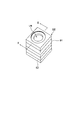
- FIG. 1 is a perspective view of an imaging apparatus LU according to the present embodiment
- FIG. 2 is a cross-sectional view of the configuration of FIG. 1 taken along the line II-II and viewed in the direction of the arrow.
- the imaging device LU is an imaging device that captures a subject image on a CMOS image sensor SR as a solid-state imaging device having a photoelectric conversion unit 51a and a photoelectric conversion unit (light receiving surface) SS of the image sensor SR.
- a lens LN and a substrate 52 having an external connection terminal (not shown) for holding the image sensor SR and transmitting / receiving the electric signal are provided, and these are integrally formed.
- the imaging lens LN includes a first lens block BK1 and a second lens block BK2 in order from the object side (upper side in FIG. 2).
- a single lens second lens may be used instead of the second lens block BK2.
- the lens blocks BK1 and BK2 are formed by connecting the lens L to two surfaces (an object side substrate surface and an image side substrate surface) facing each other on the lens substrate LS.
- continuous means that the substrate surface of the lens substrate LS and the lens L are directly bonded, or the substrate surface of the lens substrate LS and the lens L are indirectly bonded via a separate member. It means that there is.
- a photoelectric conversion unit SS as a light receiving unit in which pixels (photoelectric conversion elements) are two-dimensionally arranged is formed in the center of a plane on the light receiving side, and signal processing (not shown) is performed.
- a signal processing circuit includes a drive circuit unit that sequentially drives each pixel to obtain a signal charge, an A / D conversion unit that converts each signal charge into a digital signal, and a signal that forms an image signal output using the digital signal. It consists of a processing unit and the like.
- a number of pads (not shown) are arranged in the vicinity of the outer edge of the plane on the light receiving side of the image sensor SR, and are connected to the substrate 52 via wires (not shown).
- the image sensor SR converts the signal charge from the photoelectric conversion unit 51a into an image signal such as a digital YUV signal, and outputs it to a predetermined circuit on the substrate 52 via a wire (not shown).
- Y is a luminance signal
- the solid-state imaging device is not limited to the CMOS image sensor, and other devices such as a CCD may be used.
- the substrate 52 that supports the image sensor SR is communicably connected to the image sensor SR by a wiring (not shown).
- the substrate 52 is connected to an external circuit (for example, a control circuit included in a host device of a portable terminal mounted with an imaging device) via an external connection terminal (not shown), and a voltage for driving the image sensor SR from the external circuit. And a clock signal can be received, and a digital YUV signal can be output to an external circuit.
- an external circuit for example, a control circuit included in a host device of a portable terminal mounted with an imaging device
- an external connection terminal not shown
- a clock signal can be received, and a digital YUV signal can be output to an external circuit.
- the upper part of the image sensor SR is sealed with a plate (also referred to as a parallel plate element) PT such as an infrared cut filter fixed on the upper surface of the substrate 52.
- the lower end of the spacer member B2 is fixed to the upper surface of the plate PT.
- the second lens block BK2 is fixed to the upper end of the spacer member B2
- the lower end of another spacer member B1 is fixed to the upper surface of the second lens block BK2
- the first end of the spacer member B1 is The lens block BK1 is fixed.
- the first lens block BK1 includes a resin-made first lens substrate LS1, which is a parallel plate, and resin-made lens portions L1a, L1b fixed to the object side and the image plane side.
- the second lens block BK2 And a resin-made second lens substrate LS2, which is a parallel plate, and resin-made lens portions L2a, L2b fixed to the object side and the image plane side thereof.
- the first lens block BK1 has a positive power with the convex surface facing the object side and the concave surface facing the image side, and the image side surface of the second lens block BK2 has a positive power at the periphery.
- the first lens substrate LS1 and the second lens substrate LS2 may be glass substrates.
- the object side lens portion L1a formed on the object side surface of the first lens substrate LS1 has a convex shape on the object side.
- the image side lens portion L1b formed on the image side surface of the first lens substrate LS1 has a concave shape on the image side.
- the aperture stop S may be formed by forming a light-shielding film on the object side surface of the first lens substrate LS1 and providing a circular aperture through which light can be transmitted, but is not limited thereto.
- the object side lens portion L2a formed on the object side surface of the second lens substrate LS2 has a convex shape in the vicinity of the optical axis on the object side.
- the image side lens portion L2b formed on the image side surface of the second lens substrate LS2 has a concave shape in the vicinity of the optical axis on the image side.
- the imaging lens LN is suitable for use in a digital device with an image input function (for example, a portable terminal).
- a digital device including a combination of an imaging lens and an imaging element is an imaging device that optically captures an image of a subject and outputs it as an electrical signal.
- the imaging device is a main component (optical device) of a camera that captures still images and moving images of a subject.
- a main component optical device of a camera that captures still images and moving images of a subject.
- an imaging lens that forms an optical image of an object in order from the object (that is, subject) side, and the imaging lens
- an image sensor that converts the optical image formed by the method into an electrical signal.
- cameras examples include digital cameras, video cameras, surveillance cameras, in-vehicle cameras, and videophone cameras.
- Cameras are built into personal computers, mobile terminals (for example, compact and portable information device terminals such as mobile phones and mobile computers), peripheral devices (scanners, printers, etc.), and other digital devices. Or it may be externally attached.
- a camera is configured by mounting an imaging apparatus, but also various devices having a camera function are configured by mounting the imaging apparatus.
- a digital device with an image input function such as a mobile phone with a camera is configured.
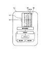
- FIG. 3 is a block diagram of a mobile terminal CU which is an example of a digital device with an image input function.
- the imaging device LU mounted on the portable terminal CU in this figure includes an imaging lens LN, a parallel plate element PT, and an image sensor SR (sometimes referred to as an imaging lens LN including the parallel plate element PT).
- the imaging lens LN forms an optical image (image plane) IM of the object in order from the object (that is, subject) side. More specifically, the imaging lens LN includes, for example, lens blocks BK1 and BK2, and forms an optical image IM on the light receiving surface SS of the image sensor SR.
- the optical image IM to be formed by the imaging lens LN passes, for example, an optical low-pass filter (parallel plate element PT in FIG. 3) having a predetermined cutoff frequency characteristic determined by the pixel pitch of the image sensor SR. To do. By this passage, the spatial frequency characteristics are adjusted so that so-called aliasing noise that occurs when converted into an electrical signal is minimized.
- an optical low-pass filter parallel plate element PT in FIG. 3
- the parallel plate element PT is, for example, an optical filter such as an optical low-pass filter or an infrared cut filter disposed as necessary (the parallel plate element PT corresponds to a cover glass or the like of the image sensor SR). There is also.)
- the image sensor SR converts the optical image IM formed on the light receiving surface SS by the imaging lens LN into an electrical signal.
- a CCD (Charge-Coupled Device) type image sensor having a plurality of pixels and a CMOS (Complementary Metal-Oxide-Semiconductor) type image sensor can be cited as the imaging device (solid-state imaging device).
- the imaging lens LN is positioned so as to form an optical image IM of the subject on the light receiving surface SS of the image sensor SR. Therefore, the optical image IM formed by the imaging lens LN is efficiently converted into an electrical signal by the image sensor SR.
- the imaging device LU when such an imaging device LU is mounted on a portable terminal CU with an image input function, the imaging device LU is usually arranged inside the body of the portable terminal CU.
- the imaging device LU takes a form as necessary.
- the unitized imaging device LU may be detachable or rotatable with respect to the main body of the mobile terminal CU.
- the mobile terminal CU includes a signal processing unit 1, a control unit 2, a memory 3, an operation unit 4, and a display unit 5 in addition to the imaging device LU.
- the signal processing unit 1 performs, for example, predetermined digital image processing and image compression processing on the signal generated by the image sensor SR as necessary.
- the processed signal is recorded as a digital video signal in the memory 3 (semiconductor memory, optical disc, etc.), or converted into an infrared signal via a cable and transmitted to another device.
- the control unit 2 is a microcomputer and performs function control such as a photographing function and an image reproduction function intensively.
- the control unit 2 controls the imaging device LU so as to perform at least one of still image shooting and moving image shooting of a subject.
- the memory 3 stores, for example, a signal generated by the image sensor SR and processed by the signal processing unit 1.
- the operation unit 4 is a part including operation members such as an operation button (for example, a release button) and an operation dial (for example, a shooting mode dial), and transmits information input by the operator to the control unit 2.
- operation members such as an operation button (for example, a release button) and an operation dial (for example, a shooting mode dial), and transmits information input by the operator to the control unit 2.
- the display unit 5 includes a display such as a liquid crystal monitor, and performs image display using an image signal converted by the image sensor SR or image information recorded in the memory 3.
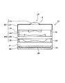
- a lens block unit UT including a plurality of lens blocks BK arranged side by side as shown in the cross-sectional view of FIG. 4A is manufactured by, for example, a replica method that can simultaneously produce a large number of lenses and is low in cost (note that The number of lens blocks BK included in the lens block unit UT may be singular or plural).
- a curable resin material is transferred in a lens shape onto a resin substrate using a mold.
- a large number of lenses are simultaneously produced on the resin substrate.
- the resin may be dropped on the entire surface to form a plurality of lenses at once with a mold, or the resin may be dropped individually and molded individually like a stamp with the same mold.
- you may manufacture not only with a replica method but with another manufacturing method.
- the imaging lens LN is manufactured from the lens block unit UT manufactured by such a method.
- An example of the manufacturing process of this imaging lens is shown in the schematic cross-sectional view of FIG.
- the first lens block unit UT1 includes a first lens substrate LS1 that is a parallel plate, a lens portion L1a that is bonded to one plane, and a lens portion L1b that is bonded to the other plane.
- the second lens block unit UT2 includes a second lens substrate LS2 that is a parallel plate, a lens portion L2a that is bonded to one plane, and a lens portion L2b that is bonded to the other plane.
- the lattice-shaped spacer member B1 is interposed between the first lens block unit UT1 and the second lens block unit UT2 (specifically, between the first lens substrate LS1 and the second lens substrate LS2). The distance between the lens block units UT1 and UT2 is kept constant. Further, the spacer member B2 is interposed between the parallel plate element PT and the second lens block unit UT2, and keeps the distance between the parallel plate element PT and the lens block unit UT2 constant (that is, the spacer members B1, B2). Is a two-stage grid). Then, the lens portions L1a to 2b are positioned in the lattice hole portions of the spacer members B1 and B2.
- the parallel plate element PT is a wafer level sensor chip size package including a microlens array, or a parallel flat plate such as a sensor cover glass or an IR cut filter (corresponding to the parallel plate element PT in FIG. 3). .
- the spacer member B1 is interposed between the first lens block unit UT1 and the first lens block unit UT2, and the spacer member B2 is interposed between the second lens block unit UT2 and the parallel plate element PT.
- the lens substrates LS (the first lens substrate LS1 and the second lens substrate LS2) are sealed and integrated.
- the imaging lens LN is manufactured by separating the members in which the plurality of lens blocks (the first lens block BK1 and the second lens block BK2) are incorporated, the lens interval for each imaging lens LN is adjusted. And no assembly is required. Therefore, mass production of the imaging lens LN is possible.
- the spacer members B1 and B2 have a lattice shape. Therefore, the spacer members B1 and B2 also serve as marks when the imaging lens LN is separated from the member in which the plurality of lens blocks BK1 and BK2 are incorporated. Therefore, the imaging lens LN is easily separated from the member in which the plurality of lens blocks BK1 and BK2 are incorporated, and it does not take time. As a result, imaging lenses can be mass-produced at low cost.
- the manufacturing method of the imaging lens LN is a connection in which the spacer member B1 is arranged on at least a part of the periphery of the lens blocks BK1 and BK2, and the plurality of lens block units UT1 and UT2 are connected through the spacer member B1. And a cutting step of cutting the connected lens block units UT1 and UT2 along the spacer member B1.
- Such a manufacturing method is suitable for mass production of an inexpensive lens system.
- the focal length of each lens portion is a value obtained under the condition that the object side and the image side of the lens are filled with air.
- the value is obtained under the condition that the object side and the image side of the lens are filled with air.
- the surface described with “*” after each surface number is a surface having an aspheric shape, and the shape of the aspheric surface has the vertex of the surface as the origin and the X axis in the optical axis direction.
- the height in the direction perpendicular to the optical axis is h, and is expressed by the following “Equation 1”.
- a radius of curvature that takes into account a secondary aspherical coefficient in the reference curvature radius of the aspherical definition formula can be regarded as a paraxial curvature radius (for example, reference literature).
- a power of 10 for example, 2.5 ⁇ 10-02
- E for example, 2.5e-002
- the surface number of the lens data was given in order with the object side of the first lens as one surface.
- the unit of the numerical value showing the length as described in an Example shall be mm.
- Example 1 Table 1 shows lens data in Example 1.
- 5 is a sectional view of the lens of Example 1.
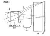
- FIG. In order from the object side, the first object side lens portion L1a, the aperture stop S, the first lens substrate LS1, and the first image side lens portion L1b constitute a first lens block BK1 having positive power, and then a single lens block BK1.
- a ball second lens L2 is disposed, and finally, a parallel plate element PT assuming a seal glass or the like of a solid-state image sensor is provided.
- IM is an imaging surface of the solid-state imaging device.
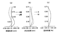
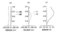
- FIG. 6 is an aberration diagram of Example 1 (spherical aberration (a), astigmatism (b), distortion (c)).
- the solid line represents the spherical aberration amount and the meridional coma aberration amount with respect to the d line and the dotted line, respectively
- the solid line represents the sagittal surface
- the dotted line represents the meridional plane (hereinafter the same).
- FIG. 7 is a sectional view of the lens of Example 2.
- the first object side lens unit L1a, the aperture stop S, the first lens substrate LS1, and the first image side lens unit L1b constitute a first lens block BK1 having a positive power.
- a ball second lens L2 is disposed, and finally, a parallel plate element PT assuming a seal glass or the like of a solid-state image sensor is provided.
- IM is an imaging surface of the solid-state imaging device.
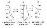
- FIG. 8 is an aberration diagram of Example 2 (spherical aberration (a), astigmatism (b), distortion (c)).
- FIG. 9 is a sectional view of the lens of Example 3.
- the first object side lens unit L1a, the aperture stop S, the first lens substrate LS1, and the image side lens unit L1b constitute a first lens block BK1, and then the second object side lens unit L2a,
- a second lens block BK2 is constituted by the second lens substrate LS2 and the second image side lens portion L2b, and finally a parallel plate element PT assuming a seal glass of a solid-state imaging element is provided.
- IM is an imaging surface of the solid-state imaging device.
- FIG. 10 is an aberration diagram of Example 3 (spherical aberration (a), astigmatism (b), distortion (c)).
- Example 4 shows lens data in Example 4.
- FIG. 11 is a sectional view of the lens of Example 4.
- the first object side lens unit L1a, the aperture stop S, the first lens substrate LS1, and the image side lens unit L1b constitute a first lens block BK1, and then the second object side lens unit L2a,
- a second lens block BK2 is constituted by the second lens substrate LS2 and the second image side lens portion L2b, and finally a parallel plate element PT assuming a seal glass of a solid-state imaging element is provided.
- IM is an imaging surface of the solid-state imaging device.
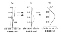
- FIG. 12 is an aberration diagram of Example 4 (spherical aberration (a), astigmatism (b), distortion (c)).
- FIG. 13 is a sectional view of the lens of Example 5.
- the first object side lens unit L1a, the aperture stop S, the first lens substrate LS1, and the image side lens unit L1b constitute a first lens block BK1, and then the second object side lens unit L2a,
- a second lens block BK2 is constituted by the second lens substrate LS2 and the second image side lens portion L2b, and finally a parallel plate element PT assuming a seal glass of a solid-state imaging element is provided.
- IM is an imaging surface of the solid-state imaging device.
- FIG. 14 is an aberration diagram of Example 5 (spherical aberration (a), astigmatism (b), distortion (c)).
- FIG. 15 is a sectional view of the lens of Example 6.
- the first object side lens unit L1a, the aperture stop S, the first lens substrate LS1, and the image side lens unit L1b constitute a first lens block BK1, and then the second object side lens unit L2a,
- a second lens block BK2 is constituted by the second lens substrate LS2 and the second image side lens portion L2b, and finally a parallel plate element PT assuming a seal glass of a solid-state imaging element is provided.
- IM is an imaging surface of the solid-state imaging device.
- FIG. 16 is an aberration diagram of Example 6 (spherical aberration (a), astigmatism (b), distortion (c)).
- FIG. 17 is a sectional view of the lens of Example 7.
- the first object side lens unit L1a, the aperture stop S, the first lens substrate LS1, and the image side lens unit L1b constitute a first lens block BK1, and then the second object side lens unit L2a,
- a second lens block BK2 is constituted by the second lens substrate LS2 and the second image side lens portion L2b, and finally a parallel plate element PT assuming a seal glass of a solid-state imaging element is provided.
- IM is an imaging surface of the solid-state imaging device.
- FIG. 18 is an aberration diagram of Example 7 (spherical aberration (a), astigmatism (b), distortion (c)).
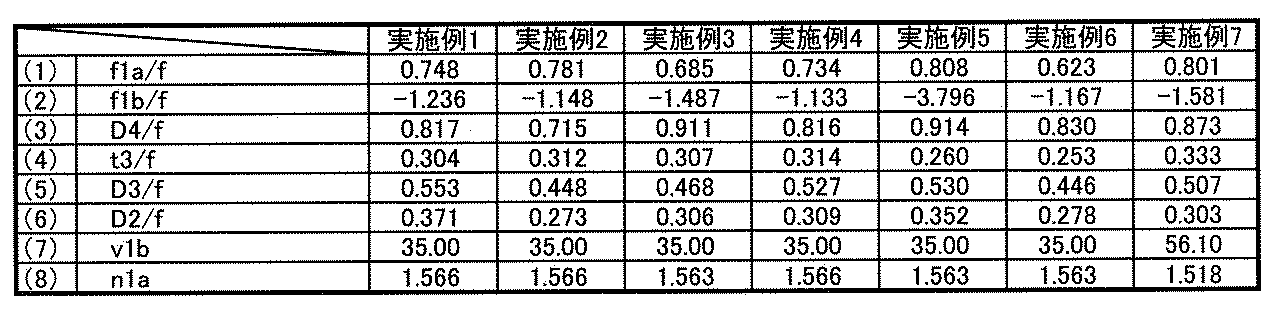
- Table 8 summarizes the values of the examples corresponding to each conditional expression.
Landscapes
- Physics & Mathematics (AREA)
- General Physics & Mathematics (AREA)
- Optics & Photonics (AREA)
- Lenses (AREA)
- Studio Devices (AREA)
Abstract
Description
0.62<fla/f<0.82 (1)
-4.00<flb/f<-1.11 (2)
0.70<D4/f<1.00 (3)
但し
fla:前記第1レンズブロック物体側レンズ部の焦点距離
flb:前記第1レンズブロック像側レンズ部の焦点距離
D4 :前記第1レンズブロック物体側面から前記第2レンズ像側面までの光軸上の距離f :前記撮像レンズ全系の焦点距離 In the imaging lens according to
0.62 <fla / f <0.82 (1)
-4.00 <flb / f <−1.11 (2)
0.70 <D4 / f <1.00 (3)
Where fla: focal length of the first lens block object side lens part flb: focal length of the first lens block image side lens part D4: on the optical axis from the first lens block object side surface to the second lens image side surface Distance f: Focal length of the entire imaging lens system
0.66<fla/f<0.77 (1’) Further, when the value of conditional expression (1) is less than the upper limit, the target optical total length can be achieved. On the other hand, when the value of conditional expression (1) exceeds the lower limit, it is possible to suppress the occurrence of higher-order aberrations due to the positive power being too strong. Preferably, the following formula is satisfied.
0.66 <fla / f <0.77 (1 ′)
-3.50<flb/f<-1.13 (2’) Furthermore, when the value of conditional expression (2) exceeds the lower limit, it is possible to prevent the occurrence of higher-order spherical aberration, coma aberration, and lateral chromatic aberration. In addition, when the radius of curvature of the image side surface of the first lens block is extremely small, when the light ray incident at an incident angle larger than the maximum image height is emitted from the side surface of the first lens block image, the emitted light beam greatly bounces. Although there is a concern that a ghost is generated by being reflected again on the side surface of the first lens block image, the occurrence of the ghost can be prevented when the value of the conditional expression (2) exceeds the lower limit. On the other hand, when the value of conditional expression (2) is less than the upper limit, the Petzval sum is reduced, and the curvature of field can be suppressed to a small value. Preferably, the following formula is satisfied.
−3.50 <flb / f <−1.13 (2 ′)
0.75<D4/f<0.95 (3’) Further, when the value of conditional expression (3) is less than the upper limit, the side surface of the second lens block image is moved away from the imaging surface, the incident height of the peripheral rays is reduced, and the effective diameter is reduced. The size of the direction can be kept small. On the other hand, when the value of conditional expression (3) exceeds the lower limit, the light ray height of the peripheral image incident on the side surface of the second lens block image becomes too low to prevent insufficient correction of field curvature. be able to. Preferably, the following formula is satisfied.
0.75 <D4 / f <0.95 (3 ′)
0.20<t3/f<0.40 (4)
但し、
t3:前記平行平板素子の厚み(前記平行平板素子を複数有する場合は、その厚みの総和とする) An imaging lens according to a fifth aspect of the present invention is the imaging lens according to any one of the first to fourth aspects, wherein a parallel plate element is provided between an image side surface of the second lens and an imaging surface of the imaging element. The flat plate element satisfies the following conditional expression.
0.20 <t3 / f <0.40 (4)
However,
t3: Thickness of the parallel plate element (when there are a plurality of the parallel plate elements, the sum of the thicknesses)
0.25<t3/f<0.35 (4’) By providing a parallel plate element between the second lens and the imaging surface of the imaging element, it is possible to prevent the dust adhering to the imaging lens from falling onto the imaging surface. In addition, by coating the parallel plate element, it is possible to provide an effect of infrared cut and reflectance reduction. When the value of conditional expression (4) is less than the upper limit, the thickness of the parallel plate element does not become too thick, and the optical total length can be prevented from becoming large. On the other hand, when the value of conditional expression (4) exceeds the lower limit, it is possible to avoid the parallel plate from becoming too thin and difficult to handle. Furthermore, it is desirable to satisfy the following equation.
0.25 <t3 / f <0.35 (4 ′)
0.43<D3/f<0.65 (5)
但し、
D3:前記第1レンズブロック物体側面から前記第2レンズ物体側面までの光軸上の距離 An imaging lens according to a seventh aspect is characterized in that, in the invention according to any one of the first to sixth aspects, the following conditional expression is satisfied.
0.43 <D3 / f <0.65 (5)
However,
D3: Distance on the optical axis from the first lens block object side surface to the second lens object side surface
0.47<D3/f<0.60 (5’) When the value of conditional expression (5) exceeds the lower limit, the object side surface of the second lens becomes closer to the imaging surface, and the incident height of the peripheral rays increases, which is advantageous for correcting astigmatism and field curvature. Become. On the other hand, when the value of conditional expression (5) is below the upper limit, it is possible to prevent the effective diameter of the second lens object side surface from becoming too large. Furthermore, it is desirable to satisfy the following conditional expression.
0.47 <D3 / f <0.60 (5 ′)
0.27<D2/f<0.50 (6)
但し
D2:前記第1レンズブロック物体側面から前記第1レンズブロック像側面までの光軸上の距離 An imaging lens according to an eighth aspect is characterized in that, in the invention according to any one of the first to seventh aspects, the following conditional expression is satisfied.
0.27 <D2 / f <0.50 (6)
D2: distance on the optical axis from the first lens block object side surface to the first lens block image side surface
0.30<D2/f<0.40 (6’) When the value of conditional expression (6) exceeds the lower limit, the thickness of the first lens block does not become too thin, and manufacturing can be facilitated. On the other hand, when the value of conditional expression (6) is less than the upper limit, the height of the axial ray incident on the side surface of the first lens block image is increased, which is advantageous for correcting chromatic aberration and spherical aberration. Furthermore, it is desirable to satisfy the following conditional expression.
0.30 <D2 / f <0.40 (6 ′)
20.0<v1b<50.0 (7)
但し、
vlb:前記第1レンズブロック像側レンズ部のアッベ数 An imaging lens according to a ninth aspect is characterized in that, in the invention according to any one of the first to eighth aspects, the following conditional expression is satisfied.
20.0 <v1b <50.0 (7)
However,
vlb: Abbe number of the first lens block image side lens portion
25.0<v1b<45.0 (7’) Optimal chromatic aberration correction can be achieved by using a material in the range of conditional expression (7). Furthermore, it is desirable to satisfy the following conditional expression.
25.0 <v1b <45.0 (7 ′)
1.54<N1a<1.65 (8)
但し、
N1a:前記第1レンズブロック物体側レンズ部のd線に対する屈折率 An imaging lens according to a tenth aspect is characterized in that, in the invention according to any one of the first to ninth aspects, the following conditional expression is satisfied.
1.54 <N1a <1.65 (8)
However,
N1a: Refractive index with respect to d-line of the first lens block object side lens portion
1.55<Nla<1.63 (8’) By using a material in the range of conditional expression (8), the overall length can be shortened and the curvature of field can be reduced. Furthermore, it is desirable to satisfy the following conditional expression.
1.55 <Nla <1.63 (8 ′)
0.62<fla/f<0.82 (1)
-4.00<f1b/f<-1.11 (2)
0.70<D4/f<1.00 (3)
但し
fla:第1レンズブロック物体側レンズ部の焦点距離
f1b:第1レンズブロック像側レンズ部の焦点距離
D4 :第1レンズブロック物体側面から第2レンズ像側面までの光軸上の距離
f :撮像レンズ全系の焦点距離 Furthermore, the following conditional expression is satisfied.
0.62 <fla / f <0.82 (1)
−4.00 <f1b / f <−1.11 (2)
0.70 <D4 / f <1.00 (3)
However, fla: focal length f1b of the first lens block object side lens part: focal length D4 of the first lens block image side lens part: distance f on the optical axis from the first lens block object side surface to the second lens image side surface f: Focal length of the entire imaging lens system
図4(a)の断面図に示すような、複数のレンズブロックBKを並べて含むレンズブロックユニットUTは、例えば、多数のレンズを同時に作製できるとともに低コストであるレプリカ法で製造される(なお、レンズブロックユニットUTに含まれるレンズブロックBKの数は単数であっても複数であってもよい)。 Hereinafter, a method for manufacturing the imaging lens LN will be described. Here, the case where the first lens block and the second lens block are manufactured by the replica method will be described. However, only the first lens block is manufactured by the replica method, and the second lens is injection-molded by a single ball and bonded to each other. You may do it.
A lens block unit UT including a plurality of lens blocks BK arranged side by side as shown in the cross-sectional view of FIG. 4A is manufactured by, for example, a replica method that can simultaneously produce a large number of lenses and is low in cost (note that The number of lens blocks BK included in the lens block unit UT may be singular or plural).
さらに、スペーサー部材B2は、平行平板素子PTと第2のレンズブロックユニットUT2との間に介在し、平行平板素子PTとレンズブロックユニットUT2との間隔を一定に保つ(つまり、スペーサー部材B1、B2は2段格子といえる)。そして、スペーサー部材B1、B2の格子の穴の部分に、各レンズ部L1a~2bが位置する。 The lattice-shaped spacer member B1 is interposed between the first lens block unit UT1 and the second lens block unit UT2 (specifically, between the first lens substrate LS1 and the second lens substrate LS2). The distance between the lens block units UT1 and UT2 is kept constant.
Further, the spacer member B2 is interposed between the parallel plate element PT and the second lens block unit UT2, and keeps the distance between the parallel plate element PT and the lens block unit UT2 constant (that is, the spacer members B1, B2). Is a two-stage grid). Then, the lens portions L1a to 2b are positioned in the lattice hole portions of the spacer members B1 and B2.
FL:撮像レンズ全系の焦点距離
Fno:Fナンバー
Ymax:固体撮像素子の撮像面対角線長
w :半画角
TL:撮像レンズ全系の最も物体側のレンズ面から像側焦点までの光軸上の距離
BF:バックフォーカス
r:曲率半径
d:軸上面間隔
nd:レンズ材料のd線に対する屈折率
vd:レンズ材料のd線に対するアッベ数 Next, examples suitable for the above-described embodiment will be described. However, the present invention is not limited to the following examples. The meaning of each symbol in the embodiment is as follows.
FL: Focal length of the entire imaging lens system
Fno: F number
Ymax: Diagonal length w of the imaging surface of the solid-state imaging device w: Half angle of view
TL: Distance on the optical axis from the most object-side lens surface to the image-side focal point of the entire imaging lens system
BF: Back focus r: Radius of curvature d: Distance between top surfaces of shaft
nd: Refractive index with respect to d-line
vd: Abbe number for the d-line of the lens material

ただし、
Ai:i次の非球面係数
R :基準曲率半径
K :円錐定数
である。
However,
Ai: i-order aspherical coefficient R: reference radius of curvature K: conic constant.
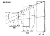
実施例1におけるレンズデータを表1に示す。図5は実施例1のレンズの断面図である。物体側から順に、第1物体側レンズ部L1a、開口絞りS、第1レンズ基板LS1、第1像側レンズ部L1bより、正のパワーを有する第1レンズブロックBK1が構成され、次に、単玉の第2レンズL2が配置され、最後に固体撮像素子のシールガラス等を想定した平行平板素子PTが設けられている。IMは固体撮像素子の撮像面である。 Example 1
Table 1 shows lens data in Example 1. 5 is a sectional view of the lens of Example 1. FIG. In order from the object side, the first object side lens portion L1a, the aperture stop S, the first lens substrate LS1, and the first image side lens portion L1b constitute a first lens block BK1 having positive power, and then a single lens block BK1. A ball second lens L2 is disposed, and finally, a parallel plate element PT assuming a seal glass or the like of a solid-state image sensor is provided. IM is an imaging surface of the solid-state imaging device.
[表1]
Reference Wave Length = 587.56 nm
unit: mm
Construction Data
NUM. r d d vd eff.diameter
OBJ INFINITY 400.0000
1* 0.4873 0.1190 1.56587 34.99 0.453
STO INFINITY 0.3089 1.51690 61.89 0.377
3 INFINITY 0.0500 1.56494 34.99 0.487
4* 0.8057 0.1591 0.520
5* 1.2157 0.3045 1.51500 51.99 0.724
6* 2.5787 0.0851 1.003
7 INFINITY 0.3500 1.47140 66.01 1.136
8 INFINITY 0.0676 1.332
IMG INFINITY 0.0329
ASPHERICAL SURFACE
1:K=1.65918e+000,A3=-7.87366e-001,A4=5.83475e+000,A5=-1.23052e+001,A6=-1.42136e+002,A8=3.02996e+003,A10=-3.57451e+004,A12=1.43968e+005
4:K=-5.65823e+001,A3=6.28068e-001,A4=3.00129e+000,A6=7.74543e+001,A8=-1.99521e+003,A10=8.84810e+003,A12=1.68638e+005,A14=2.64918e+005,A16=-1.75174e+007,A18=-1.99876e+007
5:K=-3.00000e+001,A4=-1.58845e+000,A6=-2.99162e+001,A8=5.86010e+002,A10=-5.96898e+003,A12=3.35530e+004,A14=-9.12256e+004,A16=9.30355e+004
6:K=-7.56873e+000,A4=-8.51293e-001,A6=-7.78094e+000,A8=3.84309e+001,A10=-1.23938e+002,A12=1.22997e+002,A14=1.99080e+002,A16=-6.24597e+002
FL 1.1510
Fno 2.8815
w 60.3285
Ymax 0.7140
BF 0.4235
TL 1.3650
Elem Surfs Focal Length Diameter
1 1- 4 1.401018 0.5197
2 5- 6 4.150589 1.0029
[Example 1]
[table 1]
Reference Wave Length = 587.56 nm
unit: mm
Construction Data
NUM.r d d vd eff.diameter
OBJ INFINITY 400.0000
1 * 0.4873 0.1190 1.56587 34.99 0.453
STO INFINITY 0.3089 1.51690 61.89 0.377
3 INFINITY 0.0500 1.56494 34.99 0.487
4 * 0.8057 0.1591 0.520
5 * 1.2157 0.3045 1.51500 51.99 0.724
6 * 2.5787 0.0851 1.003
7 INFINITY 0.3500 1.47140 66.01 1.136
8 INFINITY 0.0676 1.332
IMG INFINITY 0.0329
ASPHERICAL SURFACE
1: K = 1.65918e + 000, A3 = -7.87366e-001, A4 = 5.83475e + 000, A5 = -1.23052e + 001, A6 = -1.42136e + 002, A8 = 3.02996e + 003, A10 =- 3.57451e + 004, A12 = 1.43968e + 005
4: K = -5.65823e + 001, A3 = 6.28068e-001, A4 = 3.00129e + 000, A6 = 7.74543e + 001, A8 = -1.99521e + 003, A10 = 8.84810e + 003, A12 = 1.68638e + 005, A14 = 2.64918e + 005, A16 = -1.75174e + 007, A18 = -1.99876e + 007
5: K = -3.00000e + 001, A4 = -1.58845e + 000, A6 = -2.99162e + 001, A8 = 5.86010e + 002, A10 = -5.96898e + 003, A12 = 3.35530e + 004, A14 = -9.12256e + 004, A16 = 9.30355e + 004
6: K = -7.56873e + 000, A4 = -8.51293e-001, A6 = -7.78094e + 000, A8 = 3.84309e + 001, A10 = -1.23938e + 002, A12 = 1.22997e + 002, A14 = 1.99080e + 002, A16 = -6.24597e + 002
FL 1.1510
Fno 2.8815
w 60.3285
Ymax 0.7140
BF 0.4235
TL 1.3650
Elem Surfs Focal Length Diameter
1 1- 4 1.401018 0.5197
2 5- 6 4.150589 1.0029
実施例2におけるレンズデータを表2に示す。図7は実施例2のレンズの断面図である。物体側から順に、第1物体側レンズ部L1a、開口絞りS、第1レンズ基板LS1、第1像側レンズ部L1bより、正のパワーを有する第1レンズブロックBK1が構成され、次に、単玉の第2レンズL2が配置され、最後に固体撮像素子のシールガラス等を想定した平行平板素子PTが設けられている。IMは固体撮像素子の撮像面である。 (Example 2)
Table 2 shows lens data in Example 2. FIG. 7 is a sectional view of the lens of Example 2. In order from the object side, the first object side lens unit L1a, the aperture stop S, the first lens substrate LS1, and the first image side lens unit L1b constitute a first lens block BK1 having a positive power. A ball second lens L2 is disposed, and finally, a parallel plate element PT assuming a seal glass or the like of a solid-state image sensor is provided. IM is an imaging surface of the solid-state imaging device.
[表2]
Reference Wave Length = 587.56 nm
unit: mm
Construction Data
NUM. r d nd vd eff.diameter
OBJ INFINITY 400.0000
1* 0.4959 0.1058 1.56587 34.99 0.433
STO INFINITY 0.2000 1.51690 61.89 0.370
3 INFINITY 0.0500 1.56494 34.99 0.439
4* 0.7285 0.1466 0.472
5* 1.2258 0.3000 1.51500 51.99 0.650
6* -5.1894 0.0851 0.885
7 INFINITY 0.3500 1.47140 66.01 0.998
8 INFINITY 0.2238 1.184
IMG INFINITY 0.0722
ASPHERICAL SURFACE
1:K=2.83968e+000,A3=-3.99623e-001,A4=2.45457e+000,A5=-1.89676e+001,A6=-1.01073e+002,A8=3.13669e+003,A10=-4.58398e+004,A12=5.14751e+003
4:K=-1.15325e+002,A3=3.47401e+000,A4=-6.62006e+000,A6=4.35694e+001,A8=-9.79704e+002,A10=1.66214e+004,A12=8.83191e+004,A14=-2.07937e+006,A16=-4.32312e+007,A18=5.94464e+008
5:K=1.00110e+001,A4=-9.30582e-001,A6=-4.99360e+001,A8=6.32117e+002,A10=-5.61766e+003,A12=2.80249e+004,A14=-1.53557e+005,A16=4.75995e+005
6:K=1.39021e+001,A4=1.10879e+000,A6=-1.49539e+001,A8=4.35373e+001,A10=-8.99008e+001,A12=1.23256e+002,A14=-1.51511e+003,A16=3.09747e+003
FL 1.1203
Fno 2.8815
w 61.1451
Ymax 0.7140
BF 0.6126
TL 1.4149
Elem Surfs Focal Length Diameter
1 1- 4 1.753357 0.4717
2 5- 6 1.956544 0.8851
[Example 2]
[Table 2]
Reference Wave Length = 587.56 nm
unit: mm
Construction Data
NUM.r d nd vd eff.diameter
OBJ INFINITY 400.0000
1 * 0.4959 0.1058 1.56587 34.99 0.433
STO INFINITY 0.2000 1.51690 61.89 0.370
3 INFINITY 0.0500 1.56494 34.99 0.439
4 * 0.7285 0.1466 0.472
5 * 1.2258 0.3000 1.51500 51.99 0.650
6 * -5.1894 0.0851 0.885
7 INFINITY 0.3500 1.47140 66.01 0.998
8 INFINITY 0.2238 1.184
IMG INFINITY 0.0722
ASPHERICAL SURFACE
1: K = 2.83968e + 000, A3 = -3.99623e-001, A4 = 2.45457e + 000, A5 = -1.89676e + 001, A6 = -1.01073e + 002, A8 = 3.13669e + 003, A10 =- 4.58398e + 004, A12 = 5.14751e + 003
4: K = -1.15325e + 002, A3 = 3.47401e + 000, A4 = -6.62006e + 000, A6 = 4.35694e + 001, A8 = -9.79704e + 002, A10 = 1.66214e + 004, A12 = 8.83191 e + 004, A14 = -2.07937e + 006, A16 = -4.32312e + 007, A18 = 5.94464e + 008
5: K = 1.00110e + 001, A4 = -9.30582e-001, A6 = -4.99360e + 001, A8 = 6.32117e + 002, A10 = -5.61766e + 003, A12 = 2.80249e + 004, A14 =- 1.53557e + 005, A16 = 4.75995e + 005
6: K = 1.39021e + 001, A4 = 1.10879e + 000, A6 = -1.49539e + 001, A8 = 4.35373e + 001, A10 = -8.99008e + 001, A12 = 1.23256e + 002, A14 = -1.51511 e + 003, A16 = 3.09747e + 003
FL 1.1203
Fno 2.8815
w 61.1451
Ymax 0.7140
BF 0.6126
TL 1.4149
Elem Surfs Focal Length Diameter
1 1- 4 1.753357 0.4717
2 5--6 1.956544 0.8851
実施例3におけるレンズデータを表3に示す。図9は実施例3のレンズの断面図である。物体側から順に、第1物体側レンズ部L1a、開口絞りS、第1レンズ基板LS1、像側レンズ部L1bより、第1レンズブロックBK1が構成され、次に、第2物体側レンズ部L2a、第2レンズ基板LS2、第2像側レンズ部L2bより、第2レンズブロックBK2が構成され、最後に固体撮像素子のシールガラス等を想定した平行平板素子PTが設けられている。IMは固体撮像素子の撮像面である。 (Example 3)
Table 3 shows lens data in Example 3. FIG. 9 is a sectional view of the lens of Example 3. In order from the object side, the first object side lens unit L1a, the aperture stop S, the first lens substrate LS1, and the image side lens unit L1b constitute a first lens block BK1, and then the second object side lens unit L2a, A second lens block BK2 is constituted by the second lens substrate LS2 and the second image side lens portion L2b, and finally a parallel plate element PT assuming a seal glass of a solid-state imaging element is provided. IM is an imaging surface of the solid-state imaging device.
[表3]
Reference Wave Length = 587.56 nm
unit: mm
Construction Data
NUM. r d nd vd eff.diameter
OBJ INFINITY 400.0000
1* 0.4401 0.1434 1.56289 34.99 0.462
STO INFINITY 0.2052 1.52000 52.99 0.367
3 INFINITY 0.0500 1.56289 34.99 0.380
4* 0.9554 0.1358 0.416
5* -131.0666 0.0499 1.56289 34.99 0.529
6 INFINITY 0.2500 1.52000 52.99 0.616
7 INFINITY 0.2050 1.56289 34.99 0.917
8* 23.6946 0.1000 1.053
9 INFINITY 0.3000 1.47400 56.39 1.215
10 INFINITY -0.0038 1.412
IMG INFINITY 0.0200
ASPHERICAL SURFACE
1:K=2.95228e-002,A4=-1.33842e+000,A6=8.72220e+001,A8=-2.11581e+003,A10=1.70180e+004
4:K=1.03340e+001,A4=1.35867e+000,A6=-1.19278e+002,A8=4.34554e+003,A10=-4.85266e+004
5:K=1.00215e+003,A4=-4.90104e+000,A6=2.05682e+001,A8=-2.74401e+002,A10=-3.90403e+003,A12=6.36983e+004,A14=-2.57140e+005
8:K=-2.78766e+001,A4=-2.55967e-001,A6=-6.39372e+000,A8=1.76376e+001,A10=-2.56484e+001
FL 1.1412
Fno 2.8600
w 62.5392
Ymax 0.7140
BF 0.3197
TL 1.3591
Elem Surfs Focal Length Diameter
1 1- 4 1.130203 0.4620
2 5- 8 -35.607068 1.0527
[Example 3]
[Table 3]
Reference Wave Length = 587.56 nm
unit: mm
Construction Data
NUM.r d nd vd eff.diameter
OBJ INFINITY 400.0000
1 * 0.4401 0.1434 1.56289 34.99 0.462
STO INFINITY 0.2052 1.52000 52.99 0.367
3 INFINITY 0.0500 1.56289 34.99 0.380
4 * 0.9554 0.1358 0.416
5 * -131.0666 0.0499 1.56289 34.99 0.529
6 INFINITY 0.2500 1.52000 52.99 0.616
7 INFINITY 0.2050 1.56289 34.99 0.917
8 * 23.6946 0.1000 1.053
9 INFINITY 0.3000 1.47400 56.39 1.215
10 INFINITY -0.0038 1.412
IMG INFINITY 0.0200
ASPHERICAL SURFACE
1: K = 2.95228e-002, A4 = -1.33842e + 000, A6 = 8.72220e + 001, A8 = -2.11581e + 003, A10 = 1.70180e + 004
4: K = 1.03340e + 001, A4 = 1.35867e + 000, A6 = -1.19278e + 002, A8 = 4.34554e + 003, A10 = -4.85266e + 004
5: K = 1.00215e + 003, A4 = -4.90104e + 000, A6 = 2.05682e + 001, A8 = -2.74401e + 002, A10 = -3.90403e + 003, A12 = 6.36983e + 004, A14 =- 2.57140e + 005
8: K = -2.78766e + 001, A4 = -2.55967e-001, A6 = -6.39372e + 000, A8 = 1.76376e + 001, A10 = -2.56484e + 001
FL 1.1412
Fno 2.8600
w 62.5392
Ymax 0.7140
BF 0.3197
TL 1.3591
Elem Surfs Focal Length Diameter
1 1- 4 1.130 203 0.4620
2 5- 8 -35.607068 1.0527
実施例4におけるレンズデータを表4に示す。図11は実施例4のレンズの断面図である。物体側から順に、第1物体側レンズ部L1a、開口絞りS、第1レンズ基板LS1、像側レンズ部L1bより、第1レンズブロックBK1が構成され、次に、第2物体側レンズ部L2a、第2レンズ基板LS2、第2像側レンズ部L2bより、第2レンズブロックBK2が構成され、最後に固体撮像素子のシールガラス等を想定した平行平板素子PTが設けられている。IMは固体撮像素子の撮像面である。 Example 4
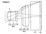
Table 4 shows lens data in Example 4. FIG. 11 is a sectional view of the lens of Example 4. In order from the object side, the first object side lens unit L1a, the aperture stop S, the first lens substrate LS1, and the image side lens unit L1b constitute a first lens block BK1, and then the second object side lens unit L2a, A second lens block BK2 is constituted by the second lens substrate LS2 and the second image side lens portion L2b, and finally a parallel plate element PT assuming a seal glass of a solid-state imaging element is provided. IM is an imaging surface of the solid-state imaging device.
[表4]
Reference Wave Length = 587.56 nm
unit: mm
Construction Data
NUM. r d nd vd eff.diameter
OBJ INFINITY 400.0000 0.000
1* 0.4630 0.1392 1.56587 34.99 0.455
STO INFINITY 0.2050 1.51690 61.89 0.357
3 INFINITY 0.0500 1.56494 34.99 0.435
4* 0.7131 0.1934 0.470
5* 1.0165 0.0733 1.56587 34.99 0.791
6 INFINITY 0.1000 1.51690 61.89 0.841
7 INFINITY 0.1489 1.51617 55.99 0.943
8* 1.9846 0.0851 1.045
9 INFINITY 0.4000 1.47140 66.01 1.156
10 INFINITY 0.0337 1.373
IMG INFINITY 0.0189
ASPHERICAL SURFACE
1:K=1.45390e+000,A3=-7.24831e-001,A4=5.42784e+000,A5=-9.58421e+000,A6=-1.33157e+002,A8=2.63640e+003,A10=-3.73321e+004,A12=2.24055e+005
4:K=-1.00860e+002,A3=1.64973e+000,A4=2.31647e+000,A6=4.49760e+001,A8=-1.97183e+003,A10=1.23904e+004,A12=2.49476e+005,A14=9.55310e+005,A16=-2.59728e+007,A18=-3.57101e+008
5:K=-3.50689e+001,A4=-3.67584e-001,A6=-3.05948e+001,A8=5.93690e+002,A10=-5.98207e+003,A12=3.31288e+004,A14=-9.31231e+004,A16=1.04191e+005
8:K=3.08075e+000,A4=-1.31342e+000,A6=-4.36704e+000,A8=3.52088e+001,A10=-1.27175e+002,A12=1.00962e+002,A14=2.54701e+002,A16=-3.05267e+002
FL 1.1147
Fno 2.8815
w 64.3536
Ymax 0.7140
BF 0.4095
TL 1.3194
Elem Surfs Focal Length Diameter
1 1- 4 1.474927 0.4705
2 5- 8 3.056598 1.0452
[Example 4]
[Table 4]
Reference Wave Length = 587.56 nm
unit: mm
Construction Data
NUM.r d nd vd eff.diameter
OBJ INFINITY 400.0000 0.000
1 * 0.4630 0.1392 1.56587 34.99 0.455
STO INFINITY 0.2050 1.51690 61.89 0.357
3 INFINITY 0.0500 1.56494 34.99 0.435
4 * 0.7131 0.1934 0.470
5 * 1.0165 0.0733 1.56587 34.99 0.791
6 INFINITY 0.1000 1.51690 61.89 0.841
7 INFINITY 0.1489 1.51617 55.99 0.943
8 * 1.9846 0.0851 1.045
9 INFINITY 0.4000 1.47140 66.01 1.156
10 INFINITY 0.0337 1.373
IMG INFINITY 0.0189
ASPHERICAL SURFACE
1: K = 1.45390e + 000, A3 = -7.24831e-001, A4 = 5.42784e + 000, A5 = -9.58421e + 000, A6 = -1.33157e + 002, A8 = 2.63640e + 003, A10 =- 3.73321e + 004, A12 = 2.24055e + 005
4: K = -1.00860e + 002, A3 = 1.64973e + 000, A4 = 2.31647e + 000, A6 = 4.49760e + 001, A8 = -1.97183e + 003, A10 = 1.23904e + 004, A12 = 2.49476e + 005, A14 = 9.55310e + 005, A16 = -2.59728e + 007, A18 = -3.57101e + 008
5: K = -3.50689e + 001, A4 = -3.67584e-001, A6 = -3.05948e + 001, A8 = 5.93690e + 002, A10 = -5.98207e + 003, A12 = 3.31288e + 004, A14 = -9.31231e + 004, A16 = 1.04191e + 005
8: K = 3.08075e + 000, A4 = -1.31342e + 000, A6 = -4.36704e + 000, A8 = 3.52088e + 001, A10 = -1.27175e + 002, A12 = 1.00962e + 002, A14 = 2.54701 e + 002, A16 = -3.05267e + 002
FL 1.1147
Fno 2.8815
w 64.3536
Ymax 0.7140
BF 0.4095
TL 1.3194
Elem Surfs Focal Length Diameter
1 1- 4 1.474927 0.4705
2 5--8 3.056598 1.0452
実施例5におけるレンズデータを表5に示す。図13は実施例5のレンズの断面図である。物体側から順に、第1物体側レンズ部L1a、開口絞りS、第1レンズ基板LS1、像側レンズ部L1bより、第1レンズブロックBK1が構成され、次に、第2物体側レンズ部L2a、第2レンズ基板LS2、第2像側レンズ部L2bより、第2レンズブロックBK2が構成され、最後に固体撮像素子のシールガラス等を想定した平行平板素子PTが設けられている。IMは固体撮像素子の撮像面である。 (Example 5)
Table 5 shows lens data in Example 5. FIG. 13 is a sectional view of the lens of Example 5. In order from the object side, the first object side lens unit L1a, the aperture stop S, the first lens substrate LS1, and the image side lens unit L1b constitute a first lens block BK1, and then the second object side lens unit L2a, A second lens block BK2 is constituted by the second lens substrate LS2 and the second image side lens portion L2b, and finally a parallel plate element PT assuming a seal glass of a solid-state imaging element is provided. IM is an imaging surface of the solid-state imaging device.
[表5]
Reference Wave Length = 587.56 nm
unit: mm
Construction Data
NUM. r d nd vd eff.diameter
OBJ INFINITY 400.0000
1* 0.5238 0.2000 1.56289 34.99 0.515
STO INFINITY 0.2050 1.52000 52.99 0.359
3 INFINITY 0.0500 1.56289 34.99 0.380
4* 2.4613 0.1551 0.413
5* -11.5163 0.0500 1.51720 56.27 0.507
6 INFINITY 0.2000 1.52000 52.99 0.637
7 INFINITY 0.1926 1.56289 34.99 0.906
8* 6.1743 0.1000 1.024
9 INFINITY 0.3000 1.47400 56.39 1.194
10 INFINITY 0.0263 1.368
IMG INFINITY 0.0270
ASPHERICAL SURFACE
1:K=-1.21742e+000,A4=-2.56387e-001,A6=7.29057e+001,A8=-3.09998e+003,A10=8.17950e+004,A12=-1.26684e+006,A14=1.02562e+007,A16=-3.23908e+007
4:K=3.00000e+001,A4=-2.26301e-001,A6=-1.14109e+002,A8=3.31290e+003,A10=-4.02841e+004,A12=-4.11162e+002,A14=-1.43176e+003,A16=2.98287e+004
5:K=-3.00000e+001,A4=-8.55698e+000,A6=6.98454e+001,A8=-4.17210e+002,A10=-4.10570e+004,A12=5.19506e+005,A14=3.41692e+006,A16=-9.23239e+007
8:K=-3.00000e+001,A4=-6.30900e-001,A6=-1.07823e+001,A8=6.64253e+001,A10=-2.41169e+002,A12=2.79477e+002,A14=4.92080e+002,A16=-1.38644e+003
FL 1.1519
Fno 2.8600
w 62.6494
Ymax 0.7140
BF 0.3498
TL 1.4026
Elem Surfs Focal Length Diameter
1 1- 4 1.088980 0.5208
2 5- 8 -7.285662 1.0644
[Example 5]
[Table 5]
Reference Wave Length = 587.56 nm
unit: mm
Construction Data
NUM.r d nd vd eff.diameter
OBJ INFINITY 400.0000
1 * 0.5238 0.2000 1.56289 34.99 0.515
STO INFINITY 0.2050 1.52000 52.99 0.359
3 INFINITY 0.0500 1.56289 34.99 0.380
4 * 2.4613 0.1551 0.413
5 * -11.5163 0.0500 1.51720 56.27 0.507
6 INFINITY 0.2000 1.52000 52.99 0.637
7 INFINITY 0.1926 1.56289 34.99 0.906
8 * 6.1743 0.1000 1.024
9 INFINITY 0.3000 1.47400 56.39 1.194
10 INFINITY 0.0263 1.368
IMG INFINITY 0.0270
ASPHERICAL SURFACE
1: K = -1.21742e + 000, A4 = -2.56387e-001, A6 = 7.29057e + 001, A8 = -3.09998e + 003, A10 = 8.17950e + 004, A12 = -1.26684e + 006, A14 = 1.02562e + 007, A16 = -3.23908e + 007
4: K = 3.00000e + 001, A4 = -2.26301e-001, A6 = -1.14109e + 002, A8 = 3.31290e + 003, A10 = -4.02841e + 004, A12 = -4.11162e + 002, A14 = -1.43176e + 003, A16 = 2.98287e + 004
5: K = -3.00000e + 001, A4 = -8.55698e + 000, A6 = 6.98454e + 001, A8 = -4.17210e + 002, A10 = -4.10570e + 004, A12 = 5.19506e + 005, A14 = 3.41692e + 006, A16 = -9.23239e + 007
8: K = -3.00000e + 001, A4 = -6.30900e-001, A6 = -1.07823e + 001, A8 = 6.64253e + 001, A10 = -2.41169e + 002, A12 = 2.79477e + 002, A14 = 4.92080e + 002, A16 = -1.38644e + 003
FL 1.1519
Fno 2.8600
w 62.6494
Ymax 0.7140
BF 0.3498
TL 1.4026
Elem Surfs Focal Length Diameter
1 1- 4 1.088980 0.5208
2 5- 8 -7.285662 1.0644
実施例6におけるレンズデータを表6に示す。図15は実施例6のレンズの断面図である。物体側から順に、第1物体側レンズ部L1a、開口絞りS、第1レンズ基板LS1、像側レンズ部L1bより、第1レンズブロックBK1が構成され、次に、第2物体側レンズ部L2a、第2レンズ基板LS2、第2像側レンズ部L2bより、第2レンズブロックBK2が構成され、最後に固体撮像素子のシールガラス等を想定した平行平板素子PTが設けられている。IMは固体撮像素子の撮像面である。 (Example 6)
Table 6 shows lens data in Example 6. FIG. 15 is a sectional view of the lens of Example 6. In order from the object side, the first object side lens unit L1a, the aperture stop S, the first lens substrate LS1, and the image side lens unit L1b constitute a first lens block BK1, and then the second object side lens unit L2a, A second lens block BK2 is constituted by the second lens substrate LS2 and the second image side lens portion L2b, and finally a parallel plate element PT assuming a seal glass of a solid-state imaging element is provided. IM is an imaging surface of the solid-state imaging device.
[表6]
Reference Wave Length = 587.56 nm
unit: mm
Construction Data
NUM. r d nd vd eff.diameter
OBJ INFINITY 400.0000
1* 0.4159 0.1195 1.56289 34.99 0.455
STO INFINITY 0.2103 1.52000 52.99 0.391
3 INFINITY 0.0550 1.56289 34.99 0.380
4* 0.7788 0.1448 0.411
5* -6.2051 0.0526 1.51720 56.27 0.532
6 INFINITY 0.2018 1.52000 52.99 0.644
7 INFINITY 0.2000 1.56289 34.99 0.908
8* -13.0253 0.1000 1.025
9 INFINITY 0.3000 1.47400 56.39 1.202
10 INFINITY 0.0431 1.369
IMG INFINITY 0.0100
ASPHERICAL SURFACE
1:K=-1.28503e+000,A4=1.23205e+000,A6=6.83314e+001,A8=-1.45208e+003,A10=1.18411e+004
4:K=4.08643e+000,A4=2.91597e+000,A6=-1.38844e+002,A8=4.76354e+003,A10=-4.16599e+004,A12=-6.30303e-003,A14=-1.08202e-001
5:K=-3.00000e+001,A4=-3.07290e+000,A6=-1.27286e+002,A8=3.64177e+003,A10=-3.72791e+004,A12=-1.44164e+005,A14=2.96669e+006
8:K=-2.99507e+001,A4=-2.44118e-001,A6=-7.94952e+000,A8=2.58503e+001,A10=-4.75500e+001
FL 1.1857
Fno 2.8600
w 60.5477
Ymax 0.7140
BF 0.3487
TL 1.3327
Elem Surfs Focal Length Diameter
1 1- 4 1.142285 0.4554
2 5- 8 -25.594240 1.0252
[Example 6]
[Table 6]
Reference Wave Length = 587.56 nm
unit: mm
Construction Data
NUM.r d nd vd eff.diameter
OBJ INFINITY 400.0000
1 * 0.4159 0.1195 1.56289 34.99 0.455
STO INFINITY 0.2103 1.52000 52.99 0.391
3 INFINITY 0.0550 1.56289 34.99 0.380
4 * 0.7788 0.1448 0.411
5 * -6.2051 0.0526 1.51720 56.27 0.532
6 INFINITY 0.2018 1.52000 52.99 0.644
7 INFINITY 0.2000 1.56289 34.99 0.908
8 * -13.0253 0.1000 1.025
9 INFINITY 0.3000 1.47400 56.39 1.202
10 INFINITY 0.0431 1.369
IMG INFINITY 0.0100
ASPHERICAL SURFACE
1: K = -1.28503e + 000, A4 = 1.23205e + 000, A6 = 6.83314e + 001, A8 = -1.45208e + 003, A10 = 1.18411e + 004
4: K = 4.08643e + 000, A4 = 2.91597e + 000, A6 = -1.38844e + 002, A8 = 4.76354e + 003, A10 = -4.16599e + 004, A12 = -6.30303e-003, A14 =- 1.08202e-001
5: K = -3.00000e + 001, A4 = -3.07290e + 000, A6 = -1.27286e + 002, A8 = 3.64177e + 003, A10 = -3.72791e + 004, A12 = -1.44164e + 005, A14 = 2.96669e + 006
8: K = -2.99507e + 001, A4 = -2.44118e-001, A6 = -7.94952e + 000, A8 = 2.58503e + 001, A10 = -4.75500e + 001
FL 1.1857
Fno 2.8600
w 60.5477
Ymax 0.7140
BF 0.3487
TL 1.3327
Elem Surfs Focal Length Diameter
1 1- 4 1.142285 0.4554
2 5--8 -25.594240 1.0252
実施例7におけるレンズデータを表7に示す。図17は実施例7のレンズの断面図である。物体側から順に、第1物体側レンズ部L1a、開口絞りS、第1レンズ基板LS1、像側レンズ部L1bより、第1レンズブロックBK1が構成され、次に、第2物体側レンズ部L2a、第2レンズ基板LS2、第2像側レンズ部L2bより、第2レンズブロックBK2が構成され、最後に固体撮像素子のシールガラス等を想定した平行平板素子PTが設けられている。IMは固体撮像素子の撮像面である。 (Example 7)
Table 7 shows lens data in Example 7. FIG. 17 is a sectional view of the lens of Example 7. In order from the object side, the first object side lens unit L1a, the aperture stop S, the first lens substrate LS1, and the image side lens unit L1b constitute a first lens block BK1, and then the second object side lens unit L2a, A second lens block BK2 is constituted by the second lens substrate LS2 and the second image side lens portion L2b, and finally a parallel plate element PT assuming a seal glass of a solid-state imaging element is provided. IM is an imaging surface of the solid-state imaging device.
[表7]
Reference Wave Length = 587.56 nm
unit: mm
Construction Data
NUM. r d nd vd eff.diameter
OBJ INFINITY 600.0000
1* 0.6236 0.1500 1.51784 56.10 0.590
STO INFINITY 0.3050 1.51000 62.39 0.494
3 INFINITY 0.1810 1.51784 56.10 0.422
4* 1.2308 0.1260 0.572
5* 1.5401 0.0580 1.51784 56.10 0.724
6 INFINITY 0.3000 1.51000 62.39 0.818
7 INFINITY 0.1920 1.51784 56.10 1.238
8* 1.8445 0.1380 1.402
9 INFINITY 0.5000 1.47140 66.01 1.630
10 INFINITY 0.0050 1.981
IMG INFINITY 0.0000
ASPHERICAL SURFACE
1:K=1.79120e+000,A3=-1.17350e+000,A4=1.81695e+001,A5=-1.30023e+002,A6=3.91848e+002,A8=-4.20685e+003,A10=8.88289e+004,A12=-1.29992e+006,A14=9.68907e+006,A16=-2.80628e+007
4:K=-3.39260e+001,A3=1.52360e+000,A4=-1.50040e+001,A5=4.69460e+001,A6=1.05630e+001,A8=-1.09630e+003,A10=9.43880e+003,A12=-3.81090e+004,A14=5.87560e+004
5:K=-7.58610e+000,A3=9.73190e-001,A4=-1.53070e+001,A5=5.35330e+001,A6=-7.00910e+001,A8=-1.44260e+002,A10=1.12470e+003,A12=6.39880e+003,A14=-8.66270e+004,A16=2.11840e+005
8:K=-5.00000e+0010,A4=-9.65860e-003,A6=-3.50620e+000,A8=1.75210e+001,A10=-6.09420e+001,A12=1.22910e+002,A14=-1.34010e+002,A16=5.83690e+001
FL 1.5029
Fno 2.8680
w 50.7006
Ymax 0.8800
BF 0.4822
TL 1.7942
Elem Surfs Focal Length Diameter
1 1- 4 1.797171 0.5900
2 5- 8 11.136791 1.4020
[Example 7]
[Table 7]
Reference Wave Length = 587.56 nm
unit: mm
Construction Data
NUM.r d nd vd eff.diameter
OBJ INFINITY 600.0000
1 * 0.6236 0.1500 1.51784 56.10 0.590
STO INFINITY 0.3050 1.51000 62.39 0.494
3 INFINITY 0.1810 1.51784 56.10 0.422
4 * 1.2308 0.1260 0.572
5 * 1.5401 0.0580 1.51784 56.10 0.724
6 INFINITY 0.3000 1.51000 62.39 0.818
7 INFINITY 0.1920 1.51784 56.10 1.238
8 * 1.8445 0.1380 1.402
9 INFINITY 0.5000 1.47140 66.01 1.630
10 INFINITY 0.0050 1.981
IMG INFINITY 0.0000
ASPHERICAL SURFACE
1: K = 1.79120e + 000, A3 = -1.17350e + 000, A4 = 1.81695e + 001, A5 = -1.30023e + 002, A6 = 3.91848e + 002, A8 = -4.20685e + 003, A10 = 8.88289 e + 004, A12 = -1.29992e + 006, A14 = 9.68907e + 006, A16 = -2.80628e + 007
4: K = -3.39260e + 001, A3 = 1.52360e + 000, A4 = -1.50040e + 001, A5 = 4.69460e + 001, A6 = 1.05630e + 001, A8 = -1.09630e + 003, A10 = 9.43880 e + 003, A12 = -3.81090e + 004, A14 = 5.87560e + 004
5: K = -7.58610e + 000, A3 = 9.73190e-001, A4 = -1.53070e + 001, A5 = 5.35330e + 001, A6 = -7.00910e + 001, A8 = -1.44260e + 002, A10 = 1.12470e + 003, A12 = 6.39880e + 003, A14 = -8.66270e + 004, A16 = 2.11840e + 005
8: K = -5.00000e + 0010, A4 = -9.65860e-003, A6 = -3.50620e + 000, A8 = 1.75210e + 001, A10 = -6.09420e + 001, A12 = 1.22910e + 002, A14 = -1.34010e + 002, A16 = 5.83690e + 001
FL 1.5029
Fno 2.8680
w 50.7006
Ymax 0.8800
BF 0.4822
TL 1.7942
Elem Surfs Focal Length Diameter
1 1- 4 1.797171 0.5900
2 5- 8 11.136791 1.4020
B1 第1スペーサー部材
B2 第2スペーサー部材
BK レンズブロック
BK1 第1レンズブロック
BK2 第2レンズブロック
L1a 第1物体側レンズ部
L1b 第1像側レンズ部
L2a 第2物体側レンズ部
L2b 第2像側レンズ部
LN 撮像レンズ
LS レンズ基板
LS1 第1レンズ基板
LS2 第2レンズ基板
LU 撮像装置
MC 撮像装置
PT 平行平板素子
S 開口絞り
SR イメージセンサ
SS 光電変換部
T 携帯電話機
UT レンズブロックユニット
UT1 第1レンズブロックユニット
UT2 第2レンズブロックユニット B Operation button B1 1st spacer member B2 2nd spacer member BK Lens block BK1 1st lens block BK2 2nd lens block L1a 1st object side lens part L1b 1st image side lens part L2a 2nd object side lens part L2b 2nd Image side lens unit LN Image pickup lens LS Lens substrate LS1 First lens substrate LS2 Second lens substrate LU Image pickup device MC Image pickup device PT Parallel plate element S Aperture stop SR Image sensor SS Photoelectric conversion unit T Mobile phone UT Lens block unit UT1 First Lens block unit UT2 Second lens block unit
Claims (13)
- 平行平板であるレンズ基板と、その物体側面および像側面のうち少なくとも一方に形成され、正または負のパワーを有するレンズ部を備える光学要素をレンズブロックと呼ぶとき、物体側から順に、物体側に凸面を向け、像側に凹面を向けた正のパワーを有する第1レンズブロック、第2レンズから構成され、開口絞りが前記第1レンズブロックの物体側、もしくは前記第1レンズブロック内部にあり、前記第2レンズの像側面は周辺部が正のパワーを持ち、下記の条件式を満たすことを特徴とする撮像レンズ。
0.62<fla/f<0.82 (1)
-4.00<flb/f<-1.11 (2)
0.70<D4/f<1.00 (3)
但し
fla:前記第1レンズブロック物体側レンズ部の焦点距離
flb:前記第1レンズブロック像側レンズ部の焦点距離
D4 :前記第1レンズブロック物体側面から前記第2レンズ像側面までの光軸上の距離f :前記撮像レンズ全系の焦点距離 When an optical element including a lens substrate that is a parallel plate and a lens unit that is formed on at least one of the object side surface and the image side surface and has a positive or negative power is called a lens block, in order from the object side to the object side. It is composed of a first lens block having a positive power with a convex surface and a concave surface facing the image side, and a second lens, and an aperture stop is located on the object side of the first lens block or inside the first lens block, An image pickup lens, wherein the image side surface of the second lens has a positive power at the periphery and satisfies the following conditional expression.
0.62 <fla / f <0.82 (1)
-4.00 <flb / f <−1.11 (2)
0.70 <D4 / f <1.00 (3)
Where fla: focal length of the first lens block object side lens part flb: focal length of the first lens block image side lens part D4: on the optical axis from the first lens block object side surface to the second lens image side surface Distance f: Focal length of the entire imaging lens system - 前記第2レンズは、平行平板であるレンズ基板と、その物体側面および像側面のうち少なくとも一方に形成され、正または負のパワーを有するレンズ部を備えるレンズブロックであることを特徴とする請求項1に記載の撮像レンズ。 The second lens is a lens block including a lens substrate that is a parallel plate and a lens unit that is formed on at least one of the object side surface and the image side surface and has a positive or negative power. The imaging lens according to 1.
- 前記第2レンズの物体側面は、光軸近傍において物体側に凸面を有することを特徴とする請求項1又は2に記載の撮像レンズ。 3. The imaging lens according to claim 1, wherein the object side surface of the second lens has a convex surface on the object side in the vicinity of the optical axis.
- 前記レンズ基板は樹脂材料から形成されていることを特徴とする請求項1~3のいずれかに記載の撮像レンズ。 The imaging lens according to any one of claims 1 to 3, wherein the lens substrate is formed of a resin material.
- 前記第2レンズの像側面と撮像素子の撮像面との間に平行平板素子を有し、前記平行平板素子は下記の条件式を満足することを特徴とする請求項1~4のいずれかに記載の撮像レンズ。
0.20<t3/f<0.40 (4)
但し、
t3:前記平行平板素子の厚み(前記平行平板素子を複数有する場合は、その厚みの総和とする) 5. The parallel plate element according to claim 1, further comprising a parallel plate element between an image side surface of the second lens and an image pickup surface of the image pickup element, wherein the parallel plate element satisfies the following conditional expression. The imaging lens described.
0.20 <t3 / f <0.40 (4)
However,
t3: Thickness of the parallel plate element (when there are a plurality of the parallel plate elements, the sum of the thicknesses) - 前記第1レンズブロックと前記第2レンズとはスペーサー部材を介して接合されており、前記スペーサー部材は樹脂材料から形成されていることを特徴とする請求項1~5のいずれかに記載の撮像レンズ。 The imaging according to any one of claims 1 to 5, wherein the first lens block and the second lens are joined via a spacer member, and the spacer member is formed of a resin material. lens.
- 以下の条件式を満足することを特徴とする請求項1~6のいずれかに記載の撮像レンズ。
0.43<D3/f<0.65 (5)
但し、
D3:前記第1レンズブロック物体側面から前記第2レンズ物体側面までの光軸上の距離 The imaging lens according to any one of claims 1 to 6, wherein the following conditional expression is satisfied.
0.43 <D3 / f <0.65 (5)
However,
D3: Distance on the optical axis from the first lens block object side surface to the second lens object side surface - 以下の条件式を満足することを特徴とする請求項1~7のいずれかに記載の撮像レンズ。
0.27<D2/f<0.50 (6)
但し
D2:前記第1レンズブロック物体側面から前記第1レンズブロック像側面までの光軸上の距離 The imaging lens according to any one of claims 1 to 7, wherein the following conditional expression is satisfied.
0.27 <D2 / f <0.50 (6)
D2: distance on the optical axis from the first lens block object side surface to the first lens block image side surface - 以下の条件式を満足することを特徴とする請求項1~8のいずれかに記載の撮像レンズ。
20.0<v1b<50.0 (7)
但し、
vlb:前記第1レンズブロック像側レンズ部のアッベ数 9. The imaging lens according to claim 1, wherein the following conditional expression is satisfied.
20.0 <v1b <50.0 (7)
However,
vlb: Abbe number of the first lens block image side lens portion - 以下の条件式を満足することを特徴とする請求項1~9のいずれかに記載の撮像レンズ。
1.54<N1a<1.65 (8)
但し、
N1a:前記第1レンズブロック物体側レンズ部のd線に対する屈折率 10. The imaging lens according to claim 1, wherein the following conditional expression is satisfied.
1.54 <N1a <1.65 (8)
However,
N1a: Refractive index with respect to d line of the first lens block object side lens portion - 実質的にパワーを持たないレンズを更に有することを特徴とする請求項1~10のいずれかに記載の撮像レンズ。 The imaging lens according to any one of claims 1 to 10, further comprising a lens having substantially no power.
- 請求項1~11のいずれかに記載の撮像レンズを備える撮像装置。 An imaging apparatus comprising the imaging lens according to any one of claims 1 to 11.
- 請求項12に記載の撮像装置を有することを特徴とする携帯端末。 A portable terminal comprising the imaging device according to claim 12.
Priority Applications (2)
| Application Number | Priority Date | Filing Date | Title |
|---|---|---|---|
| JP2013516288A JPWO2012160983A1 (en) | 2011-05-20 | 2012-05-10 | Imaging lens, imaging device, and portable terminal |
| US14/119,140 US9304293B2 (en) | 2011-05-20 | 2012-05-10 | Imaging lens, imaging apparatus and mobile terminal device |
Applications Claiming Priority (2)
| Application Number | Priority Date | Filing Date | Title |
|---|---|---|---|
| JP2011-113285 | 2011-05-20 | ||
| JP2011113285 | 2011-05-20 |
Publications (1)
| Publication Number | Publication Date |
|---|---|
| WO2012160983A1 true WO2012160983A1 (en) | 2012-11-29 |
Family
ID=47217063
Family Applications (1)
| Application Number | Title | Priority Date | Filing Date |
|---|---|---|---|
| PCT/JP2012/061963 WO2012160983A1 (en) | 2011-05-20 | 2012-05-10 | Imaging lens, imaging device, and mobile terminal |
Country Status (3)
| Country | Link |
|---|---|
| US (1) | US9304293B2 (en) |
| JP (1) | JPWO2012160983A1 (en) |
| WO (1) | WO2012160983A1 (en) |
Cited By (2)
| Publication number | Priority date | Publication date | Assignee | Title |
|---|---|---|---|---|
| US9995908B2 (en) | 2016-10-03 | 2018-06-12 | Largan Precision Co., Ltd. | Optical imaging lens system, image capturing unit and electronic device |
| US10908391B2 (en) | 2018-07-12 | 2021-02-02 | Largan Precision Co., Ltd. | Imaging optical lens assembly, image capturing unit and electronic device |
Families Citing this family (6)
| Publication number | Priority date | Publication date | Assignee | Title |
|---|---|---|---|---|
| US9377603B1 (en) * | 2015-01-26 | 2016-06-28 | Omnivision Technologies, Inc. | Low-profile hybrid lens systems and methods for manufacturing the same |
| US9897778B2 (en) * | 2016-01-12 | 2018-02-20 | Omnivision Technologies, Inc. | Four-surface narrow field-of-view compound lens |
| US10393999B2 (en) | 2016-10-06 | 2019-08-27 | Omnivision Technologies, Inc. | Six-aspheric-surface lens |
| US10718923B2 (en) * | 2016-11-10 | 2020-07-21 | Ams Sensors Singapore Pte. Ltd. | Thermally tunable optoelectronic modules |
| US10571654B2 (en) * | 2017-01-10 | 2020-02-25 | Omnivision Technologies, Inc. | Four-surface near-infrared wafer-level lens systems |
| TWI634360B (en) | 2017-09-29 | 2018-09-01 | 大立光電股份有限公司 | Electronic device |
Citations (7)
| Publication number | Priority date | Publication date | Assignee | Title |
|---|---|---|---|---|
| WO2008102648A1 (en) * | 2007-02-19 | 2008-08-28 | Konica Minolta Opto, Inc. | Imaging lens, imaging device, and mobile terminal |
| JP2009251210A (en) * | 2008-04-04 | 2009-10-29 | Konica Minolta Opto Inc | Imaging lens, imaging apparatus, electronic apparatus, portable terminal, and method for manufacturing imaging lens |
| JP2010054810A (en) * | 2008-08-28 | 2010-03-11 | Konica Minolta Opto Inc | Image pickup lens, image pickup apparatus, and mobile terminal |
| JP2010092022A (en) * | 2008-10-09 | 2010-04-22 | Visera Technologies Co Ltd | Miniature image capture lens |
| JP2010117387A (en) * | 2008-11-11 | 2010-05-27 | Seikoh Giken Co Ltd | Imaging lens |
| WO2010143458A1 (en) * | 2009-06-10 | 2010-12-16 | コニカミノルタオプト株式会社 | Image pickup lens and image pickup device |
| JP2011022494A (en) * | 2009-07-17 | 2011-02-03 | Konica Minolta Opto Inc | Image pickup lens, image pickup apparatus, mobile terminal, method for manufacturing image pickup lens and method for manufacturing image pickup apparatus |
Family Cites Families (1)
| Publication number | Priority date | Publication date | Assignee | Title |
|---|---|---|---|---|
| KR100764434B1 (en) | 2006-10-16 | 2007-10-05 | 삼성전기주식회사 | Subminiature optical system |
-
2012
- 2012-05-10 US US14/119,140 patent/US9304293B2/en active Active
- 2012-05-10 JP JP2013516288A patent/JPWO2012160983A1/en active Pending
- 2012-05-10 WO PCT/JP2012/061963 patent/WO2012160983A1/en active Application Filing
Patent Citations (7)
| Publication number | Priority date | Publication date | Assignee | Title |
|---|---|---|---|---|
| WO2008102648A1 (en) * | 2007-02-19 | 2008-08-28 | Konica Minolta Opto, Inc. | Imaging lens, imaging device, and mobile terminal |
| JP2009251210A (en) * | 2008-04-04 | 2009-10-29 | Konica Minolta Opto Inc | Imaging lens, imaging apparatus, electronic apparatus, portable terminal, and method for manufacturing imaging lens |
| JP2010054810A (en) * | 2008-08-28 | 2010-03-11 | Konica Minolta Opto Inc | Image pickup lens, image pickup apparatus, and mobile terminal |
| JP2010092022A (en) * | 2008-10-09 | 2010-04-22 | Visera Technologies Co Ltd | Miniature image capture lens |
| JP2010117387A (en) * | 2008-11-11 | 2010-05-27 | Seikoh Giken Co Ltd | Imaging lens |
| WO2010143458A1 (en) * | 2009-06-10 | 2010-12-16 | コニカミノルタオプト株式会社 | Image pickup lens and image pickup device |
| JP2011022494A (en) * | 2009-07-17 | 2011-02-03 | Konica Minolta Opto Inc | Image pickup lens, image pickup apparatus, mobile terminal, method for manufacturing image pickup lens and method for manufacturing image pickup apparatus |
Cited By (3)
| Publication number | Priority date | Publication date | Assignee | Title |
|---|---|---|---|---|
| US9995908B2 (en) | 2016-10-03 | 2018-06-12 | Largan Precision Co., Ltd. | Optical imaging lens system, image capturing unit and electronic device |
| US10908391B2 (en) | 2018-07-12 | 2021-02-02 | Largan Precision Co., Ltd. | Imaging optical lens assembly, image capturing unit and electronic device |
| US11822056B2 (en) | 2018-07-12 | 2023-11-21 | Largan Precision Co., Ltd. | Imaging optical lens assembly, image capturing unit and electronic device |
Also Published As
| Publication number | Publication date |
|---|---|
| JPWO2012160983A1 (en) | 2014-07-31 |
| US9304293B2 (en) | 2016-04-05 |
| US20140192424A1 (en) | 2014-07-10 |
Similar Documents
| Publication | Publication Date | Title |
|---|---|---|
| JP5321954B2 (en) | Imaging lens, imaging device, and portable terminal | |
| JP4513924B2 (en) | Imaging lens, imaging device, portable terminal, and manufacturing method of imaging lens | |
| JP5348563B2 (en) | Imaging lens, imaging device, and portable terminal | |
| JP5413738B2 (en) | Imaging lens, imaging device, and portable terminal | |
| JP5267825B2 (en) | IMAGING LENS, IMAGING DEVICE, DIGITAL DEVICE, AND IMAGING LENS MANUFACTURING METHOD | |
| JP5434093B2 (en) | Imaging lens, imaging device, and portable terminal | |
| WO2012160983A1 (en) | Imaging lens, imaging device, and mobile terminal | |
| WO2014175058A1 (en) | Imaging lens, imaging device, and mobile terminal | |
| WO2010010891A1 (en) | Image pickup lens, image pickup device and portable terminal device | |
| WO2009104669A1 (en) | Imaging lens, imaging apparatus, portable terminal, and method for producing imaging lens | |
| WO2009101928A1 (en) | Lens unit, image capturing lens, image capturing device, and portable terminal | |
| JP2008233884A (en) | Imaging lens, imaging device, portable terminal and method for manufacturing imaging lens | |
| JP2011017764A (en) | Imaging lens, imaging apparatus and portable terminal | |
| JP5648689B2 (en) | Imaging lens and imaging apparatus | |
| WO2010047178A1 (en) | Imaging lens, imaging device, and portable terminal | |
| JPWO2009069467A1 (en) | Imaging lens, imaging device, and portable terminal | |
| JP2010266815A (en) | Imaging lens, image capturing apparatus and mobile terminal | |
| WO2012173026A1 (en) | Image capture lens for image capture device and image capture device | |
| JP5391822B2 (en) | Imaging lens, imaging device, and portable terminal | |
| JP5267773B2 (en) | IMAGING LENS, IMAGING DEVICE, DIGITAL DEVICE, AND IMAGING LENS MANUFACTURING METHOD | |
| WO2010146899A1 (en) | Image taking lens, image taking device, and portable terminal | |
| WO2010140415A1 (en) | Image taking lens, image taking device, and portable terminal | |
| WO2010087084A1 (en) | Image pickup lens, image pickup apapratus, and portable terminal | |
| WO2010134376A1 (en) | Image pickup lens, image pickup device, and portable terminal | |
| JP2013218353A (en) | Image capturing lens, image capturing device, and mobile terminal |
Legal Events
| Date | Code | Title | Description |
|---|---|---|---|
| 121 | Ep: the epo has been informed by wipo that ep was designated in this application |
Ref document number: 12789421 Country of ref document: EP Kind code of ref document: A1 |
|
| ENP | Entry into the national phase |
Ref document number: 2013516288 Country of ref document: JP Kind code of ref document: A |
|
| NENP | Non-entry into the national phase |
Ref country code: DE |
|
| WWE | Wipo information: entry into national phase |
Ref document number: 14119140 Country of ref document: US |
|
| 122 | Ep: pct application non-entry in european phase |
Ref document number: 12789421 Country of ref document: EP Kind code of ref document: A1 |