WO2012157649A1 - 表示装置 - Google Patents
表示装置 Download PDFInfo
- Publication number
- WO2012157649A1 WO2012157649A1 PCT/JP2012/062432 JP2012062432W WO2012157649A1 WO 2012157649 A1 WO2012157649 A1 WO 2012157649A1 JP 2012062432 W JP2012062432 W JP 2012062432W WO 2012157649 A1 WO2012157649 A1 WO 2012157649A1
- Authority
- WO
- WIPO (PCT)
- Prior art keywords
- board
- signal
- inter
- fail
- timing controller
- Prior art date
- Legal status (The legal status is an assumption and is not a legal conclusion. Google has not performed a legal analysis and makes no representation as to the accuracy of the status listed.)
- Ceased
Links
Images





Classifications
-
- G—PHYSICS
- G09—EDUCATION; CRYPTOGRAPHY; DISPLAY; ADVERTISING; SEALS
- G09G—ARRANGEMENTS OR CIRCUITS FOR CONTROL OF INDICATING DEVICES USING STATIC MEANS TO PRESENT VARIABLE INFORMATION
- G09G3/00—Control arrangements or circuits, of interest only in connection with visual indicators other than cathode-ray tubes
- G09G3/20—Control arrangements or circuits, of interest only in connection with visual indicators other than cathode-ray tubes for presentation of an assembly of a number of characters, e.g. a page, by composing the assembly by combination of individual elements arranged in a matrix no fixed position being assigned to or needed to be assigned to the individual characters or partial characters
- G09G3/34—Control arrangements or circuits, of interest only in connection with visual indicators other than cathode-ray tubes for presentation of an assembly of a number of characters, e.g. a page, by composing the assembly by combination of individual elements arranged in a matrix no fixed position being assigned to or needed to be assigned to the individual characters or partial characters by control of light from an independent source
- G09G3/36—Control arrangements or circuits, of interest only in connection with visual indicators other than cathode-ray tubes for presentation of an assembly of a number of characters, e.g. a page, by composing the assembly by combination of individual elements arranged in a matrix no fixed position being assigned to or needed to be assigned to the individual characters or partial characters by control of light from an independent source using liquid crystals
- G09G3/3611—Control of matrices with row and column drivers
- G09G3/3648—Control of matrices with row and column drivers using an active matrix
- G09G3/3655—Details of drivers for counter electrodes, e.g. common electrodes for pixel capacitors or supplementary storage capacitors
-
- G—PHYSICS
- G09—EDUCATION; CRYPTOGRAPHY; DISPLAY; ADVERTISING; SEALS
- G09G—ARRANGEMENTS OR CIRCUITS FOR CONTROL OF INDICATING DEVICES USING STATIC MEANS TO PRESENT VARIABLE INFORMATION
- G09G3/00—Control arrangements or circuits, of interest only in connection with visual indicators other than cathode-ray tubes
- G09G3/20—Control arrangements or circuits, of interest only in connection with visual indicators other than cathode-ray tubes for presentation of an assembly of a number of characters, e.g. a page, by composing the assembly by combination of individual elements arranged in a matrix no fixed position being assigned to or needed to be assigned to the individual characters or partial characters
- G09G3/34—Control arrangements or circuits, of interest only in connection with visual indicators other than cathode-ray tubes for presentation of an assembly of a number of characters, e.g. a page, by composing the assembly by combination of individual elements arranged in a matrix no fixed position being assigned to or needed to be assigned to the individual characters or partial characters by control of light from an independent source
- G09G3/36—Control arrangements or circuits, of interest only in connection with visual indicators other than cathode-ray tubes for presentation of an assembly of a number of characters, e.g. a page, by composing the assembly by combination of individual elements arranged in a matrix no fixed position being assigned to or needed to be assigned to the individual characters or partial characters by control of light from an independent source using liquid crystals
- G09G3/3611—Control of matrices with row and column drivers
- G09G3/3648—Control of matrices with row and column drivers using an active matrix
- G09G3/3666—Control of matrices with row and column drivers using an active matrix with the matrix divided into sections
-
- G—PHYSICS
- G09—EDUCATION; CRYPTOGRAPHY; DISPLAY; ADVERTISING; SEALS
- G09G—ARRANGEMENTS OR CIRCUITS FOR CONTROL OF INDICATING DEVICES USING STATIC MEANS TO PRESENT VARIABLE INFORMATION
- G09G2300/00—Aspects of the constitution of display devices
- G09G2300/02—Composition of display devices
- G09G2300/026—Video wall, i.e. juxtaposition of a plurality of screens to create a display screen of bigger dimensions
-
- G—PHYSICS
- G09—EDUCATION; CRYPTOGRAPHY; DISPLAY; ADVERTISING; SEALS
- G09G—ARRANGEMENTS OR CIRCUITS FOR CONTROL OF INDICATING DEVICES USING STATIC MEANS TO PRESENT VARIABLE INFORMATION
- G09G2300/00—Aspects of the constitution of display devices
- G09G2300/08—Active matrix structure, i.e. with use of active elements, inclusive of non-linear two terminal elements, in the pixels together with light emitting or modulating elements
- G09G2300/0876—Supplementary capacities in pixels having special driving circuits and electrodes instead of being connected to common electrode or ground; Use of additional capacitively coupled compensation electrodes
-
- G—PHYSICS
- G09—EDUCATION; CRYPTOGRAPHY; DISPLAY; ADVERTISING; SEALS
- G09G—ARRANGEMENTS OR CIRCUITS FOR CONTROL OF INDICATING DEVICES USING STATIC MEANS TO PRESENT VARIABLE INFORMATION
- G09G2330/00—Aspects of power supply; Aspects of display protection and defect management
- G09G2330/04—Display protection
-
- G—PHYSICS
- G09—EDUCATION; CRYPTOGRAPHY; DISPLAY; ADVERTISING; SEALS
- G09G—ARRANGEMENTS OR CIRCUITS FOR CONTROL OF INDICATING DEVICES USING STATIC MEANS TO PRESENT VARIABLE INFORMATION
- G09G2360/00—Aspects of the architecture of display systems
- G09G2360/04—Display device controller operating with a plurality of display units
-
- G—PHYSICS
- G09—EDUCATION; CRYPTOGRAPHY; DISPLAY; ADVERTISING; SEALS
- G09G—ARRANGEMENTS OR CIRCUITS FOR CONTROL OF INDICATING DEVICES USING STATIC MEANS TO PRESENT VARIABLE INFORMATION
- G09G2360/00—Aspects of the architecture of display systems
- G09G2360/06—Use of more than one graphics processor to process data before displaying to one or more screens
-
- G—PHYSICS
- G09—EDUCATION; CRYPTOGRAPHY; DISPLAY; ADVERTISING; SEALS
- G09G—ARRANGEMENTS OR CIRCUITS FOR CONTROL OF INDICATING DEVICES USING STATIC MEANS TO PRESENT VARIABLE INFORMATION
- G09G5/00—Control arrangements or circuits for visual indicators common to cathode-ray tube indicators and other visual indicators
- G09G5/18—Timing circuits for raster scan displays
Definitions
- the present invention relates to a display device equipped with a plurality of timing controllers.
- the display screen is divided into multiple partial display areas in order to cope with the shortening of the writing time to each pixel accompanying the high definition of the liquid crystal display device and the dullness of the signal waveform accompanying the enlargement of the liquid crystal display device.
- a configuration (screen division method) for driving display areas separately has been proposed (see, for example, Patent Documents 1 to 3).
- this screen division method for example, one screen is divided vertically (the upper area is the first area and the lower area is the second area), the first half of the frame (upper side) is displayed in the first area, and the second The second half (lower side) of the frame is displayed in the area.
- QFHD Quant Full High Definition
- 4K2K a standard of SHV (Super Hi-Vision or UHDTV: Ultra High Definition Television)
- 8K4K a standard of SHV (Super Hi-Vision or UHDTV: Ultra High Definition Television)
- the timing controller does not prepare for output of the video signal normally for some reason, an image may not be displayed only in the partial display area corresponding to the timing controller. For example, an abnormality occurred in the operation of the timing controller itself, when the power was turned on, the device in the previous stage of the timing controller was not yet started and no video signal was input, or the operation of one of the devices in the previous stage was abnormal It is conceivable that the timing of the video signal input to the timing controller is not appropriate due to the occurrence of the error or the video signal input to the display device being inappropriate.
- the timing of the video signal is not appropriate, for example, the sync width, front porch width, back porch width, effective period of the horizontal synchronization signal, or the sync width, front porch width, back porch width of the vertical synchronization signal, and effective This indicates that the period or DataEnable signal is not appropriate.
- the timing of the video signal input to a certain timing controller is not appropriate, there is a possibility that the display of the corresponding partial display area will fail. For this reason, it is preferable not to display an image of the entire display area (for example, to display black) rather than to display an image in a state where some displays are not normal.
- the present invention has been made in view of the above-described problems, and the object thereof is a display device that performs parallel processing of video data by a plurality of timing controllers when an abnormality occurs in any of the timing controllers.
- An object of the present invention is to realize a display device capable of preventing inappropriate display.
- a display device includes a display unit including a first region and a second region, a first substrate provided with a first timing controller that performs display control of the first region, and display control of the second region.
- a second board provided with a second timing controller for performing the above-described operation, and an inter-board connection unit for connecting the first board and the second board, wherein the first timing controller controls display of the first area. If an abnormality occurs, a fail-safe signal is transmitted to the inter-board connection section to notify the second timing controller that the abnormality has occurred.
- the 1st timing controller and the 2nd timing controller can perform suitable treatment (for example, self-running control) to the above-mentioned abnormality.
- the occurrence of an abnormality in the display control of the first timing controller provided on the first substrate can be transmitted to the second timing controller provided on another second substrate.
- the 1st timing controller and the 2nd timing controller can perform suitable treatment (for example, self-running control) to the above-mentioned abnormality.
- FIG. 1 is a block diagram illustrating an overall configuration of a display device according to an embodiment of the present invention. It is a block diagram which shows the detailed structure of the pixel of the said display apparatus. It is a table
- the liquid crystal display device LCD according to the present embodiment corresponds to a video standard having a pixel number (8K4K) that is 16 times the number of full HD pixels (for example, Super Hi-Vision having a resolution of horizontal 7680 pixels ⁇ vertical 4320 pixels).
- an input processing circuit IPC an input processing circuit IPC, a pixel mapping circuit PMC, four display control boards (timing controller boards) DC1 to DC4, a liquid crystal panel (display unit) LCP, four gate drivers GD1 to GD4, 2 One source driver SD1 to SD2, four CS drivers CD1 to CD4, three power supply devices (not shown) connected to different commercial power sources, a power supply controller (not shown), a backlight BL, and a backlight driver BLD And a backlight controller BLC.
- IPC input processing circuit
- a pixel mapping circuit PMC four display control boards (timing controller boards) DC1 to DC4, a liquid crystal panel (display unit) LCP, four gate drivers GD1 to GD4, 2 One source driver SD1 to SD2, four CS drivers CD1 to CD4, three power supply devices (not shown) connected to different commercial power sources, a power supply controller (not shown), a backlight BL, and a backlight driver BLD And a backlight controller BLC.
- the video signal input to the input processing circuit IPC may be a video signal (for example, Super Hi-Vision) having a block scan format of 8K4K pixels, or a video signal having a number of 8K4K pixels of a multi-display format. Also good. Of course, it may be a video signal having the number of 4K2K pixels or a video signal having the number of 2K1K pixels (the number of full HD pixels).
- the block scan format is a method in which one frame (entire image having 8K4K pixels) is divided into 16 coarse (full HD pixel) whole images (so-called thinned images) and transmitted.
- each of the 16 video signals Qa1 to Qa16 input to the input processing circuit IPC is a rough overall image (the number of full HD pixels).
- the multi-display format is a system in which one frame (entire image having the number of 8K4K pixels) is divided into 16 without changing the fineness of the frame, and divided into 16 partial images for transmission.
- each of the 16 video signals Qa1 to Qa16 input to the input processing circuit IPC is a fine partial image (the number of full HD pixels).
- the input processing circuit IPC performs video data synchronization processing, ⁇ correction processing, color temperature correction processing, color gamut conversion processing, and the like, and outputs video signals Qb1 to Qb16 to the pixel mapping circuit PMC.
- the display control board DC1 includes two video processing circuits EP1 and EP2 and two timing controllers TC1 and TC2, and the display control board DC2 includes two video processing circuits EP3 and EP4 and two timing controllers TC3 and TC4.
- the display control board DC3 includes two video processing circuits EP5 and EP6 and two timing controllers TC5 and TC6, and the display control board DC4 includes two video processing circuits EP7 and EP8 and two timing controllers TC7 and TC8. Is provided.
- the pixel mapping circuit PMC generates two video signals (number of pixels 2K2K) corresponding to the left half AR1 of the first region (upper left region when the liquid crystal panel LCP is divided into upper, lower, left, and right) into four (full HD pixel number images).
- the video signal Qc3 / Qc4) is divided and output to the video processing circuit EP2 of the display control board DC1, and the video corresponding to the left half AR3 of the second region (the upper right region when the liquid crystal panel LCP is divided into four parts vertically and horizontally)
- the signal (number of pixels 2K2K) is divided into two (video signals Qc5 and Qc6 having the number of full HD pixels) and output to the video processing circuit EP3 of the display control board DC2, and the right half of the second area
- the video signal (number of pixels 2K2K) corresponding to AR4 is divided into two (video signals Qc7 and Qc8 having the number of full HD pixels) and output to the video processing circuit EP4 of the display control board DC2, and the third region (liquid crystal panel) Display control board by
- the video signal (number of pixels 2K2K) corresponding to the right half AR6 of the third region is divided into two (video signals Qc11 and Qc12 having the number of full HD pixels) and output to the video processing circuit EP5 of DC3.
- the video signal (number of pixels 2K2K) corresponding to the left half AR7 of the fourth area (the lower right area when the liquid crystal panel LCP is divided into four parts vertically and horizontally) is output to the video processing circuit EP6 of the substrate DC3.
- the image signal is divided into two (video signals Qc13 and Qc14 having the number of full HD pixels) and output to the video processing circuit EP7 of the display control board DC4, and the video signal (pixel number 2K2K) corresponding to the right half AR8 of the fourth region is output. It is divided into two (video signals Qc15 and Qc16 having the number of full HD pixels) and output to the video processing circuit EP8 of the display control board DC4.
- the pixel mapping circuit PMC outputs a synchronization signal SYS (vertical synchronization signal, horizontal synchronization signal, clock signal, data enable signal, polarity inversion signal, etc.) to the timing controller TC1 of the display control board DC1, and receives this timing.
- the controller TC1 transmits this synchronization signal SYS to the inter-substrate shared line SSL connected to the display control substrates DC1 to DC4.
- the timing controller TC1 receives the synchronization signal SYS received from the pixel mapping circuit PMC and cooperates with the video processing circuit EP1 to perform video processing such as gradation conversion processing and frame rate conversion (FRC) processing on the video signals Qc1 and Qc2.
- the source control signal SC1 is output to the source driver substrate (not shown) corresponding to AR1
- the gate control signal GC1 is output to the gate driver substrate (not shown) of the gate driver GD1
- the CS driver CD1 is output.
- the CS control signal CC1 is output.
- the timing controller TC2 receives the synchronization signal SYS transmitted from the timing controller TC1 via the inter-substrate shared line SSL, cooperates with the video processing circuit EP2, performs the video processing on the video signals Qc3 and Qc4, and then performs AR2
- a source control signal SC2 is output to a source driver board (not shown) corresponding to
- the timing controller TC3 receives the synchronization signal SYS transmitted from the timing controller TC1 via the inter-substrate shared line SSL, cooperates with the video processing circuit EP3, performs the video processing on the video signals Qc5 and Qc6, and then performs AR3.
- a source control signal SC3 is output to a source driver board (not shown) corresponding to
- the timing controller TC4 receives the synchronization signal SYS transmitted from the timing controller TC1 via the inter-substrate shared line SSL, cooperates with the video processing circuit EP4, performs the video processing on the video signals Qc7 and Qc8, and then performs AR4.
- the source control signal SC4 is output to the source driver board (not shown) corresponding to the above, the gate control signal GC2 is output to the gate driver board (not shown) of the gate driver GD2, and the CS control signal CC2 is sent to the CS driver CD2. Output.
- the timing controller TC5 receives the synchronization signal SYS transmitted from the timing controller TC1 via the inter-substrate shared line SSL, cooperates with the video processing circuit EP5, performs the video processing on the video signals Qc9 and Qc10, and then performs AR5.
- the source control signal SC5 is output to the source driver board (not shown) corresponding to the above, the gate control signal GC3 is output to the gate driver board (not shown) of the gate driver GD3, and the CS control signal CC3 is sent to the CS driver CD3. Output.
- the timing controller TC6 receives the synchronization signal SYS transmitted from the timing controller TC1 via the inter-substrate shared line SSL, cooperates with the video processing circuit EP6, performs the video processing on the video signals Qc11 and Qc12, and then performs AR6.
- a source control signal SC6 is output to a source driver board (not shown) corresponding to
- the timing controller TC7 receives the synchronization signal SYS transmitted from the timing controller TC1 via the inter-substrate shared line SSL, cooperates with the video processing circuit EP7, performs the video processing on the video signals Qc13 and Qc14, and then performs AR7.
- a source control signal SC7 is output to a source driver board (not shown) corresponding to
- the timing controller TC8 receives the synchronization signal SYS transmitted from the timing controller TC1 via the inter-substrate shared line SSL, cooperates with the video processing circuit EP8, performs the video processing on the video signals Qc15 and Qc16, and then performs AR8.
- the source control signal SC8 is output to the source driver board (not shown) corresponding to the above, the gate control signal GC4 is output to the gate driver board (not shown) of the gate driver GD4, and the CS control signal CC4 is sent to the CS driver CD4. Output.
- the source control signals SC1 to SC8 include a data signal, a data enable signal (DE signal), a source start pulse, and a source clock.
- the gate control signals GC1 to GC4 include an initial signal, a gate start pulse, and a gate. A clock is included.
- the fail-safe signal transmitted from the display control board in which the abnormality has occurred is transmitted to all other display control boards. And all the display control boards instantaneously enter the self-running (black display) mode. Thereby, the video failure is avoided.
- the liquid crystal panel LCP includes an active matrix substrate, a liquid crystal layer (not shown), and a counter substrate (not shown).
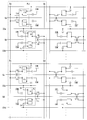
- the active matrix substrate includes a plurality of pixel electrodes (not shown) and a plurality of TFTs (thin film transistors, FIG. Scanning signal lines Ga to Gd extending in the row direction (the direction along the long side of the panel), a plurality of data signal lines Sa to Sd extending in the column direction, and a storage capacitor wiring (CS wiring extending in the row direction).
- CSa to CSd and CS trunk wires Ma to Mh extending in the column direction are provided, and a common electrode (not shown), a color filter, and a black matrix (not shown) are provided on the counter substrate. .
- the liquid crystal panel LCP is provided with two data signal lines corresponding to the upper half (upstream side of the panel) of one pixel column, and 2 corresponding to the lower half (downstream side of the panel) of this pixel column. It has a so-called upper / lower divided double source structure (a structure in which four data signal lines are provided per pixel column and four scanning signal lines can be selected simultaneously) provided with two data signal lines. Quadruple speed drive is possible. Furthermore, the liquid crystal panel LCP is a so-called multi-pixel method in which at least two pixel electrodes are provided in one pixel, and the viewing angle characteristics can be enhanced by a bright region and a dark region formed in one pixel. ing.
- scanning signal lines Ga and Gb and storage capacitor lines CSa and CSb are provided in the upper half (upstream side) of the panel, and scanning signals are provided in the lower half (downstream side) of the panel.
- Lines Gc and Gd and storage capacitor lines CSc and CSd are provided, and the upper half (upstream side) of one pixel column PL1 includes two pixels Pa and Pb adjacent in the column direction, and the lower half of the pixel column PL1
- Two pixels Pc and Pd adjacent in the column direction are included on the (downstream side)
- data signal lines Sa and Sb are provided corresponding to the upper half (upstream side) of the pixel column PL1, and below the pixel column PL1.
- Data signal lines Sc and Sd are provided corresponding to the half (downstream side).
- the TFT 12A connected to the pixel electrode 17A and the TFT 12a connected to the pixel electrode 17a are connected to the data signal line Sa and the scanning signal line Ga, respectively.
- 17A forms a storage capacitor line and a storage capacitor
- the pixel electrode 17a forms a storage capacitor line CSa and a storage capacitor
- the TFT 12B is connected to the pixel electrode 17B of the two pixel electrodes 17B and 17b included in the pixel Pb.
- the TFT 12b connected to the pixel electrode 17b is connected to the data signal line Sb and the scanning signal line Gb, the pixel electrode 17B forms the storage capacitor line CSa and the storage capacitor, and the pixel electrode 17b holds the storage capacitor line CSb.
- a capacitor is formed, and an image of the two pixel electrodes 17C and 17c included in the pixel Pc is further formed.
- the TFT 12C connected to the electrode 17C and the TFT 12c connected to the pixel electrode 17c are respectively connected to the data signal line Sc and the scanning signal line Gc, the pixel electrode 17C forms a storage capacitor line and a storage capacitor, and the pixel electrode 17c holds The capacitor wiring CSc and the storage capacitor are formed, and the TFT 12D connected to the pixel electrode 17D and the TFT 12d connected to the pixel electrode 17d of the two pixel electrodes 17D and 17d included in the pixel Pd are scanned with the data signal line Sd.
- the pixel electrode 17D forms a storage capacitor line CSc and a storage capacitor, and the pixel electrode 17d forms a storage capacitor line CSd and a storage capacitor.
- the four scanning signal lines Ga to Gd are connected to the signal line Gd. Selected at the same time.
- the scanning signal line Gc is The scanning signal line Gb is the M + 2161th line in the (M + 2160) th line counted from the upper long side, and the Mth line data signal of the Nth frame is written in the scanning signal line Ga provided in the upper half of the panel. Then, the data signal of the (M + 2160) th line of the (N ⁇ 1) th frame, which is the previous frame, is written to the scanning signal line Gc provided in the lower half of the panel.
- the polarity of the data signal supplied to one data signal line is inverted every vertical scanning period (1V), and is supplied to one and the other of the two adjacent data signal lines in the same vertical scanning period.
- the polarity of the data signal is reversed.
- each data signal line is inverted by 1V (that is, the polarity inversion period is lengthened and power consumption is reduced), and the polarity distribution of the pixels in the screen is inverted by dots (thus turning off the TFT). Flicker caused by the pull-in voltage generated at the same time can be suppressed).
- the gate driver GD1 includes a plurality of gate driver chips I provided along one of the two short sides of the upper half of the liquid crystal panel LCP and arranged in the column direction.
- the vertical driver GD2 includes a plurality of gate driver chips I provided along the other of the two short sides of the upper half of the liquid crystal panel LCP and arranged in the column direction.
- the gate driver GD3 includes a plurality of gate driver chips I provided along one of the two short sides of the lower half of the liquid crystal panel LCP and arranged in the column direction.
- the vertical driver GD4 is provided along the other of the two short sides of the lower half of the liquid crystal panel LCP, and includes a plurality of gate driver chips I arranged in the column direction.
- the scanning signal lines provided in the upper half of the panel are driven by the gate drivers GD1 and GD2, and the scanning signal lines provided in the lower half of the panel are driven by the gate drivers GD3 and GD4. That is, one scanning signal line is connected to two gate drivers arranged on both sides thereof, and a scanning (pulse) signal having the same phase is supplied from the two gate drivers to the one scanning signal line. By so doing, it is possible to suppress variations in signal dullness (the degree of signal dullness varies depending on the position in the row direction) caused by CR (time constant) of the scanning signal line.
- the source driver SD1 is provided along one long side of the upper half of the liquid crystal panel LCP, and 48 source driver chips J arranged in the row direction (the number of output terminals of one source driver chip is 960), 4 source driver boards (not shown) are included (12 source driver chips J are mounted on one source driver board).
- the source driver SD2 is provided along one long side of the lower half of the liquid crystal panel LCP, and 48 source driver chips J arranged in the row direction (the number of output terminals of one source driver chip is 960). And four source driver boards (not shown) (12 source driver chips J are mounted on one source driver board).
- Each data signal line provided in the upper half of the panel is driven by the source driver SD1, and each data signal line provided in the lower half of the panel is driven by the source driver SD2.
- the data signal line Sa is driven by the source driver SD1
- the data signal line Sc is driven by the source driver SD2.
- the source driver chip J cannot be arranged along the long side of the panel due to the space, it is arranged on the short side of the panel with sufficient space (the source driver chip J and the gate driver chip I are arranged side by side). Can be arranged).
- a relay line that connects the data signal line and the source terminal on the short side of the panel is provided on the counter substrate side, or other than the source layer of the active matrix substrate (the source / drain electrode formation layer of the TFT) It can also be provided in a lower layer (gate layer) of the gate insulating film or a layer between the source layer and the ITO layer (pixel electrode formation layer).
- the CS trunk lines Ma and Mb are provided close to one of the two short sides of the upper half of the active matrix substrate, and are driven by the CS driver CD1 so that each has a different phase.
- the CS trunk lines Mc and Md are provided close to the other of the two short sides of the upper half of the active matrix substrate, and are driven by the CS driver CD2 so that each has a different phase.
- the CS trunk lines Me and Mf are provided close to one of the two short sides of the lower half of the active matrix substrate, and are driven by the CS driver CD3 so that each has a different phase.
- the CS trunk wiring Mg ⁇ Mh is provided close to the other of the two short sides of the lower half of the active matrix substrate, and is driven by the CS driver CD4 so that each has a different phase.
- One storage capacitor line is connected to two CS trunk lines arranged on both sides thereof, and a modulation (pulse) signal having the same phase is transmitted from the two CS trunk lines to the one storage capacitor line. Is supplied.
- the storage capacitor line CSa is connected to the CS trunk lines Ma and Mc
- the storage capacitor line CSb is connected to the CS trunk lines Mb and Md
- the storage capacitor line CSc is connected to the CS trunk lines Me and Mg
- the storage capacitor line CSd is connected to CS trunk lines Mf and Mh. Therefore, for example, when the potentials of the CS trunk lines Ma and Mb are controlled to be in opposite phases, the potentials of the storage capacitor lines CSa and CSb are also reversed in phase, and in the pixel Pb, the pixel electrode of the two pixel electrodes 17B and 17b.
- the four display control boards DC1 to DC4 process in parallel video data corresponding to two partial display areas of the eight partial display areas AR1 to AR8, respectively.
- Each of the display control boards DC1 to DC4 controls the display of the partial display areas AR1 to AR8 that are different from each other.
- the entire display area is set to the free-running (black display) mode to appropriately control the display of the entire display area. Therefore, it is necessary to share abnormality information among the display control boards DC1 to DC4. Also, in order to control the display of the entire display area at the same time (black display or the like), immediacy is required for sharing abnormality information.
- the fail safe signal is a signal for the timing controllers TC1 to TC8 to perform an operation (self-running control) according to the abnormal state when an abnormality occurs. Whether the certain timing controller is in a normal state or an abnormal state Is a signal for transmitting to other timing controllers. Even if an abnormality occurs in any of the timing controllers TC1 to TC8, in order for all the timing controllers TC1 to TC8 to share the abnormality information, bidirectional communication must be possible.
- the two timing controllers may be connected by wired-or connection using a single-ended signal line. Then, by transmitting and receiving a fail safe signal between two timing controllers mounted on one board, it is possible to share abnormality information.
- each IC chip constituting a plurality of timing controllers arranged close to each other in the substrate may be connected by a signal line.
- timing controllers when a plurality of timing controllers are mounted on different boards as in this embodiment, when the plurality of boards are located apart from each other, a signal that connects the timing controllers (transmits a fail-safe signal) Lines will be placed extending long between the substrates. When the signal line becomes long, there arises a problem that it is easily affected by external noise.
- FIG. 1 is a block diagram showing a detailed configuration of the display control board.
- FIG. 1 only the configuration of the four display control boards DC1 to DC4 is shown, and the other components are not shown.
- illustration of outputs from the timing controllers TC1 to TC8 to the outside of each display control board is omitted.
- the display control board DC1 includes two video processing circuits EP1 and EP2, two timing controllers TC1 and TC2, and one inter-board signal sharing circuit (interface unit) SH1.
- the display control board DC2 includes two video processing circuits EP3 and EP4, two timing controllers TC3 and TC4, and one inter-board signal sharing circuit SH2.
- the display control board DC3 includes two video processing circuits EP5 and EP6, two timing controllers TC5 and TC6, and one inter-board signal sharing circuit SH3.
- the display control board DC4 includes two video processing circuits EP7 and EP8, two timing controllers TC7 and TC8, and one inter-board signal sharing circuit SH4. Since the display control boards DC1 to DC4 are arranged close to the positions of the corresponding partial display areas AR1 to AR8 and the corresponding source driver chip J, they are separated from each other.
- the inter-substrate signal sharing circuit SH1 includes an input / output switching unit IFS1, an LVDS (Low voltage differential) driver (differential signal output unit) LD1, and an LVDS receiver (differential signal input unit) LR1.
- the LVDS driver LD1 and the LVDS receiver LR1 constitute a differential signal transmission / reception unit as a set.
- the inter-substrate signal sharing circuit SH2 includes an input / output switching unit IFS2, an LVDS driver LD2, and an LVDS receiver LR2.
- the inter-substrate signal sharing circuit SH3 includes an input / output switching unit IFS3, an LVDS driver LD3, and an LVDS receiver LR3.
- the inter-substrate signal sharing circuit SH4 includes an input / output switching unit IFS4, an LVDS driver LD4, and an LVDS receiver LR4.
- the LVDS receivers LR1 to LR4 are Type-2 specification multi-point LVDS.
- the Type-2 specification (with fail-safe function) multipoint LVDS receiver is a receiver obtained by offsetting a High / Low determination threshold by 100 mV, and an input with a potential difference of 0 V is determined to be Low.
- the fail-safe function of the Type-2 specification mentioned here is not related to the fail-safe signal of the present invention.
- the LVDS drivers LD1 to LD4 and the LVDS receivers LR1 to LR4 are multi-point connected to a pair of inter-substrate signal lines (inter-substrate connection portions) for transmitting differential signals.
- the inter-substrate signal sharing circuits SH1 to SH4 are connected to each other.
- a termination resistor is provided between a pair of inter-substrate signal lines in the vicinity of two LVDS receivers LR1 and LR3 (located at both ends of the bus) among the LVDS receivers LR1 to LR4.
- Each LVDS driver LD1 to LD4 is always supplied with an H level voltage as a voltage to be used for output.
- the video processing circuits EP1 to EP8 perform various types of video processing in cooperation with the timing controllers TC1 to TC8, respectively, as described above.
- the timing controller TC1 monitors whether or not the video processing for the video signals Qc1 and Qc2 of a certain frame is completed at a predetermined timing (within a predetermined period). That is, when the source control signal SC1, the gate control signal GC1, and the CS control signal CC1 are ready to be output at a predetermined timing, the timing controllers TC1 to TC8 normally perform the input of the video signal and the video processing. Is determined to be in a normal state. In the normal state, the control signals are output from the timing controllers TC1 to TC8 to the drivers without delay, and the video is displayed normally.
- the timing controllers TC1 to TC8 perform video signal input or video processing. It is determined that the state is not performed normally (abnormal state). The timing controllers TC1 to TC8 that are in an abnormal state cannot output a control signal at a normal timing. Therefore, in order to control the display of each of the partial display areas AR1 to AR8 so as to prevent the video display from failing, the timing controller determined to be in an abnormal state needs to notify the other timing controllers of the abnormal state. .
- the timing controller TC1, timing controller TC2 and inter-board signal sharing circuit SH1 mounted on the same display control board DC1 are connected by wired-or connection using a single-end in-board signal line.
- the timing controller TC1, the timing controller TC2, and the inter-substrate signal sharing circuit SH1 transmit and receive an in-board fail-safe signal via the in-board signal line.
- the outputs of the timing controllers TC1 and TC2 and the inter-board signal sharing circuit SH1 to the in-board signal line are OFF, and the in-board fail-safe signal is DISABLE (invalid). Is maintained at the H level.
- the timing controllers TC1 and TC2 set the in-board signal line ports of the timing controllers TC1 and TC2 as input ports. As a result, the timing controllers TC1 and TC2 monitor the ENABLE (valid) / DISABLE (invalid) (voltage level of the signal line in the board) of the in-board failsafe signal.
- the timing controllers TC1 and TC2 enter a self-running mode and generate a control signal for self-running control according to a preset timing inside itself without depending on the input signal.
- a control signal for self-running control (a source control signal including a gate control signal and a black video data signal) is output to each driver, and the corresponding partial display areas AR1 and AR2 are displayed in black.
- the timing controllers TC1 and TC2 determine that they are in an abnormal state, the in-board signal line ports of the timing controllers TC1 and TC2 are set as output ports, and the in-board fail-safe signal is set to ENABLE (valid). That is, the voltage of the signal line in the substrate is driven to L level (Low).
- the timing controllers TC1 and TC2 enter the free-running mode. Then, a control signal for self-running control is output to each driver, and the corresponding partial display areas AR1 and AR2 are displayed in black.
- the input / output switching unit IFS1 transmits a fail-safe signal from the timing controllers TC1 and TC2 in the display control board DC1 to the timing controllers TC3 to TC8 outside the display control board DC1, and outside the display control board DC1. It plays a role of switching between modes transmitted from the timing controllers TC3 to TC8 to the timing controllers TC1 and TC2 in the display control board DC1.
- the input / output switching unit IFS1 sets the in-board signal line side port of the inter-board signal sharing circuit SH1 as an input port. Then, the input / output switching unit IFS1 of the inter-substrate signal sharing circuit SH1 monitors the ENABLE (valid) / DISABLE (invalid) (voltage level of the intra-substrate signal line) of the intra-board fail safe signal.
- the input / output switching unit IFS1 When the in-board failsafe signal is DISABLE (invalid), the input / output switching unit IFS1 outputs an input / output control signal (L level) for driver / receiver switching to the LVDS driver LD1 and the LVDS receiver LR1. When the in-board failsafe signal is ENABLE (valid), the input / output switching unit IFS1 outputs an input / output control signal (H level) to the LVDS driver LD1 and the LVDS receiver LR1.
- the input / output switching unit IFS1 sets the in-board signal line side port of the inter-board signal sharing circuit SH1 as an output port,
- the in-board fail-safe signal is set to ENABLE (valid), that is, the voltage of the in-board signal line is driven to L level.
- the LVDS driver LD1 When the input / output control signal is at the L level, the LVDS driver LD1 becomes inactive and the LVDS receiver LR1 becomes active. That is, the inter-substrate signal line side (LVDS driver LD1 and LVDS receiver LR1) of the inter-substrate signal sharing circuit SH1 is set to the input mode. Therefore, the differential signal (inter-board fail-safe signal) of the pair of inter-board signal lines is the L level (DISABLE (invalid)) of the pair of inter-substrate signal lines in the Type-2 specification of the M-LVDS type receiver. Is smaller than the threshold).
- the LVDS driver LD1 becomes active and the LVDS receiver LR1 becomes inactive.
- the inter-substrate signal line side of the inter-substrate signal sharing circuit SH1 is set to the output mode. Accordingly, the differential signal of the pair of inter-substrate signal lines is at the H level (the positive polarity potential of the pair of inter-substrate signal lines is higher than the negative polarity by a threshold value, for example, in FIG. (+ Polarity) is higher than the threshold of signal 2 (-polarity) by a threshold). At this time, the inter-board fail-safe signal is ENABLE (valid).
- LVDS receiver LR1 in the input mode receives the inter-board fail-safe signal and outputs a signal corresponding to the inter-board fail-safe signal to the input / output switching unit IFS1. That is, when the inter-board failsafe signal is DISABLE (invalid) (L level), the LVDS receiver LR1 in the input mode outputs an L level signal to the input / output switching unit IFS1. When the inter-board fail safe signal is ENABLE (valid) (H level), the LVDS receiver LR1 in the input mode outputs an H level signal to the input / output switching unit IFS1.
- the states of the inter-substrate signal sharing circuit SH1 and the inter-substrate signal sharing circuit SH2 when all the timing controllers TC1 to TC8 are in the normal state are as shown in the table of FIG.
- both the intra-board fail safe signal and the inter-board fail safe signal are DISABLE (invalid).
- the in-substrate signal line side port is set as an input port.
- the input / output control signals output by the input / output switching units IFS1 and IFS2 are at the L level, and the inter-substrate signal line side (LVDS drivers LD1 and LD2 and LVDS receivers LR1 and LR2) is set to the input mode.
- the timing controller TC1 When the timing controller TC1 is in an abnormal state, it is assumed that an abnormality occurs in the processing of the video processing circuit EP1, the video signal input to the timing controller TC1 is not appropriate, and the timing controller TC1 determines that it is in an abnormal state. At this time, the timing controller TC1 changes itself to the self-running mode. Further, the timing controller TC1 sets the in-board signal line port of the timing controller TC1 as an output port, and drives the in-board fail-safe signal to ENABLE (valid) (L level). When the timing controller TC2 detects that the in-board fail safe signal of the display control board DC1 is ENABLE (valid), it changes itself to the self-running mode.
- the input / output switching unit IFS1 detects that the in-board failsafe signal is ENABLE (valid), it outputs an input / output control signal (H level) to the LVDS driver LD1 and the LVDS receiver LR1.
- LVDS driver LD1 to which an input / output control signal of H level is input becomes active, and LVDS receiver LR1 becomes inactive. That is, the inter-substrate signal line side of the inter-substrate signal sharing circuit SH1 is set to the output mode.
- the LVDS driver LD1 outputs an inter-board fail safe signal ENABLE (valid) (H level).
- the LVDS receiver LR2 of the display control board DC2 in the input mode detects that the inter-board failsafe signal is ENABLE (valid), and outputs an H level signal to the input / output switching unit IFS2.
- the input / output switching unit IFS2 to which the H level signal is input from the LVDS receiver LR2 sets the in-board signal line side port of the inter-board signal sharing circuit SH2 as an output port, and the in-board fail-safe signal of the display control board DC2 Is driven to ENABLE (valid) (L level).
- timing controllers TC3 and TC4 detect that the in-board fail-safe signal of the display control board DC2 is ENABLE (valid), the timing controllers TC3 and TC4 change to the self-running mode.
- timing controllers TC5 to TC8 are similarly changed to the self-running mode.
- the states of the inter-substrate signal sharing circuit SH1 and the inter-substrate signal sharing circuit SH2 are as shown in the table of FIG.
- both the intra-board fail safe signal and the inter-board fail safe signal are ENABLE (valid).
- the intra-substrate signal line side port is set as an input port.
- the in-substrate signal line side port is set as an output port.
- the input / output control signal output by the input / output switching unit IFS1 is at the H level, and the inter-substrate signal line side (LVDS driver LD1 and LVDS receiver LR1) of the inter-substrate signal sharing circuit SH1 is set to the output mode.
- the input / output control signal output by the input / output switching unit IFS2 is at the L level, and the inter-substrate signal line side (LVDS driver LD2 and LVDS receiver LR2) of the inter-substrate signal sharing circuit SH2 is set to the input mode.
- timing controllers TC1 to TC8 are provided. Immediately transmitted to TC8. Therefore, all the timing controllers TC1 to TC8 are immediately changed to the free-running mode. For this reason, in the present embodiment, it is possible to prevent an inappropriate display in which the display of some partial display areas and the display of other partial display areas are not consistent. Further, since the scanning signal lines Ga to Gd and the storage capacitor lines (CS lines) CSa to CSd are not divided into the partial display areas AR1 to AR8, the timing controllers TC1 to TC8 are gated at different timings.
- the liquid crystal panel LCP may be damaged.
- the timing controllers TC1 to TC8 detect an abnormality, all the timing controllers TC1 to TC8 operate in the free-running mode. Therefore, damage to the liquid crystal panel LCP can be prevented.
- Timing controller TC1 changes its own self-running mode to a normal operation mode when normal operation becomes possible and the abnormal state is resolved. Further, the timing controller TC1 sets the in-board signal line port of the timing controller TC1 as an input port, and sets the in-board failsafe signal to DISABLE (invalid) (H level). When the timing controller TC2 detects that the in-board fail-safe signal of the display control board DC1 is DISABLE (invalid), the timing controller TC2 changes its own self-running mode to the normal operation mode.
- the input / output switching unit IFS1 outputs an input / output control signal (L level) to the LVDS driver LD1 and the LVDS receiver LR1 when detecting that the in-board failsafe signal of the display control board DC1 is DISABLE (invalid).
- LVDS driver LD1 to which an L level input / output control signal is input becomes inactive, and LVDS receiver LR1 becomes active. That is, the inter-substrate signal line side of the inter-substrate signal sharing circuit SH1 is set to the input mode. As a result, the LVDS driver LD1 is deactivated, and the inter-board fail safe signal is switched to DISABLE (invalid) (L level).
- the LVDS receiver LR2 of the display control board DC2 in the input mode detects that the inter-board failsafe signal has been switched to DISABLE (invalid), and outputs an L level signal to the input / output switching unit IFS2.
- the input / output switching unit IFS2 to which the L level signal is input from the LVDS receiver LR2 sets the in-board signal line side port of the inter-board signal sharing circuit SH2 as an input port, and the in-board fail-safe signal of the display control board DC2 To DISABLE (invalid) (H level).
- timing controllers TC3 and TC4 When the timing controllers TC3 and TC4 detect that the in-board fail-safe signal of the display control board DC2 is DISABLE (invalid), the timing controllers TC3 and TC4 change their own free-running mode to the normal operation mode. Similarly, the self-running modes of the timing controllers TC5 to TC8 of the other display control boards DC3 to DC4 are also released.
- the self-running mode of all timing controllers TC1 to TC8 is canceled, and normal video display is performed.
- the return from the self-running mode when the abnormal state is resolved is also quickly performed in all the timing controllers TC1 to TC8 in the same manner as when the abnormal state occurs. Therefore, the period in the self-running mode can be minimized.
- timing controllers TC1 and TC3 are in an abnormal state
- a case where an abnormal state has occurred in the timing controller TC3 mounted on a different display control board DC2 from the state shown in FIG. 5 where the abnormal state has occurred in the timing controller TC1 will be described below. This is also the case when the abnormal state is detected almost simultaneously (TC1 is slightly faster) in the timing controllers TC1 and TC3.
- the timing controller TC3 is in the free-running mode.
- the timing controller TC3 changes the in-board signal line port of the timing controller TC3 from the input port to the output port, and displays
- the in-board fail-safe signal of the control board DC2 is driven to ENABLE (valid) (L level). Since the input / output switching unit IFS2 originally drives the in-board fail-safe signal of the display control board DC2 to ENABLE (valid) (L level), there is no change in the in-board fail-safe signal.
- the in-board signal lines are wired or connected, there is no problem even if any of the timing controller and the display control board individually outputs L level.
- the timing controller nor the display control board outputs an L level signal to the in-board signal line, the in-board signal line is pulled up by the resistor and thus becomes the H level.
- the input / output switching unit IFS2 has already set the in-board signal line side of the inter-board signal sharing circuit SH2 as an output port due to the abnormal state of the timing controller TC1. Therefore, the state does not change any more.
- the timing controller TC3 of the display control board DC2 different from the timing controller TC1 of the display control board DC1 becomes in an abnormal state completely simultaneously, for example, the LVDS drivers LD1 and LD2 of both display control boards DC1 and DC2
- the inter-board fail-safe signal ENABLE (valid) (H level) may be output.
- the timing controllers TC1 to TC8 of all the display control boards DC1 to DC4 are in the free-running mode.
- the inter-board signal line that transmits inter-board fail-safe signals is also wired-or-connected for differential signal characteristics (that is, using the Type-2 specification (with fail-safe function) of the M-LVDS type receiver). Therefore, there is no problem even if there is the same level output from both ends.
- timing controllers TC1 and TC3 are both in the free-running mode.
- Timing controller TC1 changes its own self-running mode to a normal operation mode once normal operation becomes possible and the abnormal state is resolved. Further, the timing controller TC1 sets the in-board signal line port of the timing controller TC1 as an input port, and sets the in-board failsafe signal to DISABLE (invalid) (H level). When the timing controller TC2 detects that the in-board fail-safe signal of the display control board DC1 is DISABLE (invalid), the timing controller TC2 changes its own self-running mode to the normal operation mode.
- the input / output switching unit IFS1 outputs an input / output control signal (L level) to the LVDS driver LD1 and the LVDS receiver LR1 when detecting that the in-board failsafe signal of the display control board DC1 is DISABLE (invalid).
- LVDS driver LD1 to which an L level input / output control signal is input becomes inactive, and LVDS receiver LR1 becomes active. That is, the inter-substrate signal line side of the inter-substrate signal sharing circuit SH1 is set to the input mode. As a result, the LVDS driver LD1 is deactivated, and the inter-board fail safe signal is switched to DISABLE (invalid) (L level).
- the LVDS receiver LR2 of the display control board DC2 in the input mode detects that the inter-board failsafe signal has been switched to DISABLE (invalid), and outputs an L level signal to the input / output switching unit IFS2.
- the input / output switching unit IFS2 to which the L level signal is input from the LVDS receiver LR2 sets the in-board signal line side port of the inter-board signal sharing circuit SH2 as an input port.
- the in-board fail safe signal of the inter-board signal sharing circuit SH2 is driven to ENABLE (valid) (L level) by the timing controller TC3 in an abnormal state. Therefore, the input / output switching unit IFS2 detects that the in-board fail-safe signal of the inter-board signal sharing circuit SH2 is ENABLE (valid), and sends an input / output control signal (H level) to the LVDS driver LD2 and the LVDS receiver LR2. Is output.
- LVDS driver LD2 to which an H level input / output control signal is input becomes active, and LVDS receiver LR2 becomes inactive. That is, the inter-substrate signal line side of the inter-substrate signal sharing circuit SH2 is set to the output mode.
- the LVDS driver LD2 outputs an inter-board fail safe signal ENABLE (valid) (H level).
- the LVDS receiver LR1 of the display control board DC1 that has been in the input mode detects that the inter-board failsafe signal is ENABLE (valid), and outputs an H level signal to the input / output switching unit IFS1.
- the input / output switching unit IFS1 to which the H level signal is input from the LVDS receiver LR1 sets the in-board signal line side port of the inter-board signal sharing circuit SH1 as an output port, and the in-board fail-safe signal of the display control board DC1 Is driven to ENABLE (valid) (L level).
- the timing controllers TC1 and TC2 When the timing controllers TC1 and TC2 detect that the in-board fail-safe signal of the display control board DC1 is ENABLE (valid), the timing controllers TC1 and TC2 change to the self-running mode. As described above, the timing controllers TC1 and TC2 receive the inter-board fail-safe signal ENABLE (valid) from the display control board DC2 in which the abnormal state continues even if the free-running mode is once canceled, and immediately enter the free-running mode. Return.
- timing controllers TC5 to TC8 are similarly maintained in the self-running mode.
- the states of the inter-substrate signal sharing circuit SH1 and the inter-substrate signal sharing circuit SH2 are as shown in the table of FIG.
- the normal state is the same as when the abnormal state occurs only in the timing controller TC3.
- the input / output switching units IFS1 to IFS4 transmit and receive the inter-board failsafe signal (LVDS drivers LD1 to LD4) according to the in-board failsafe signal indicating an abnormality in the board. And the input mode / output mode of the LVDS receivers LR1 to LR4) are switched. Therefore, the fail-safe signal can be quickly transmitted and received in both directions between the substrates and within the substrate. Therefore, if any of the timing controllers is in an abnormal state, all the timing controllers TC1 to TC8 are quickly controlled to perform self-running control.
- timing controllers TC1 to TC8 are controlled to perform self-running control, and immediately after the abnormal state of all the timing controllers TC1 to TC8 is resolved, It is possible to cancel the self-running mode and perform normal video display.
- the configuration in which the inter-board fail-safe signal is transmitted using the differential signal has been described.
- the inter-board signal sharing circuit of different display control boards is connected by a single-end inter-board signal line.
- An inter-fail safe signal may be transmitted.
- the inter-substrate signal line is wired or connected in the same manner as the in-substrate signal line.
- two timing controllers mounted on different display control boards can be directly connected by a single-ended signal line wired or connected to transmit a fail-safe signal in both directions. In this case, there is no need to switch the input / output mode, and the configuration is simplified.
- liquid crystal display device was demonstrated above, this invention is applicable not only to this but a plasma panel display or an organic electroluminescent display.
- FIG. 8 is a block diagram showing a detailed configuration of the display control board of the present embodiment.
- FIG. 8 only the configuration of the four display control boards DC1 to DC4 is shown, and the other constituent members are not shown.
- illustration of outputs from the timing controllers TC1 to TC8 to the outside of each display control board is omitted.
- the display control board DC1 includes two video processing circuits EP1 and EP2, two timing controllers TC1 and TC2, and one inter-board signal sharing circuit SHA1.
- the display control board DC2 includes two video processing circuits EP3 and EP4, two timing controllers TC3 and TC4, and one inter-substrate signal sharing circuit SHA2.
- the display control board DC3 includes two video processing circuits EP5 and EP6, two timing controllers TC5 and TC6, and one inter-board signal sharing circuit SHA3.
- the display control board DC4 includes two video processing circuits EP7 and EP8, two timing controllers TC7 and TC8, and one inter-substrate signal sharing circuit SHA4. Since the display control boards DC1 to DC4 are arranged close to the positions of the corresponding partial display areas AR1 to AR8 and the corresponding source driver chip J, they are separated from each other.
- the inter-substrate signal sharing circuit SHA1 and the inter-substrate signal sharing circuit SHA2 are connected by a pair of inter-substrate signal lines for transmitting a differential signal from the inter-substrate signal sharing circuit SHA1 to the inter-substrate signal sharing circuit SHA2. (In FIG. 8, a single line is omitted).
- the inter-substrate signal sharing circuit SHA2 and the inter-substrate signal sharing circuit SHA4 are connected by a pair of inter-substrate signal lines for transmitting a differential signal from the inter-substrate signal sharing circuit SHA2 to the inter-substrate signal sharing circuit SHA4. .
- the inter-substrate signal sharing circuit SHA4 and the inter-substrate signal sharing circuit SHA3 are connected by a pair of inter-substrate signal lines for transmitting a differential signal from the inter-substrate signal sharing circuit SHA4 to the inter-substrate signal sharing circuit SHA3.
- the inter-substrate signal sharing circuit SHA3 and the inter-substrate signal sharing circuit SHA1 are connected by a pair of inter-substrate signal lines for transmitting a differential signal from the inter-substrate signal sharing circuit SHA3 to the inter-substrate signal sharing circuit SHA1. .
- These inter-substrate signal lines transmit signals only in one direction. It can be said that these inter-substrate signal lines are included in inter-substrate connection portions that connect the inter-substrate signal sharing circuits SHA1 to SHA4.
- the timing controller TC1, the timing controller TC2, and the inter-board signal sharing circuit SHA1 mounted on the same display control board DC1 are connected by wired-or connection using a single-end in-board signal line.
- the timing controller TC1, the timing controller TC2, and the inter-substrate signal sharing circuit SHA1 transmit and receive an in-board fail-safe signal via the in-board signal line.
- the in-board fail-safe signal is DISABLE (invalid), that is, the voltage of the in-board signal line is maintained at the H level.
- timing controllers TC1 and TC2 The operation of the timing controllers TC1 and TC2 is the same as that of the first embodiment.
- the inter-board fail safe signal is DISABLE (invalid) (H level)
- the inter-board fail safe signal from the inter-board signal sharing circuit SHA3 is DISABLE (invalid) (L level).
- the inter-board signal sharing circuit SHA1 sets the inter-board fail safe signal to the inter-board signal sharing circuit SHA2 to DISABLE (invalid) (L level).
- the inter-board signal sharing circuit SHA1 detects that the in-board fail-safe signal is ENABLE (valid) (L level)
- the inter-board signal sharing circuit SHA1 detects the LVDS driver connected to one end of the inter-board signal line (
- the inter-board fail-safe signal ENABLE (valid) (H level) is output to the inter-board signal sharing circuit SHA2 by an unshown).
- the inter-substrate signal sharing circuit SHA1 detects that the inter-substrate fail-safe signal from the inter-substrate signal sharing circuit SHA3 is ENABLE (H level)
- the inter-substrate signal sharing circuit SHA1 The inter-board fail safe signal ENABLE (valid) is output to the shared circuit SHA2, and the in-board signal line side port is set as an output port, and the intra-board fail safe signal ENABLE (valid) (L level) is sent to the timing controllers TC1 and TC2. ) Is output.
- the inter-board signal sharing circuits SHA1 to SHA4 receive the inter-board fail-safe signal ENABLE (valid) from the other inter-board signal sharing circuits, the next inter-board signal sharing is connected in a ring shape by the inter-board signal line. Since the inter-board fail-safe signal ENABLE (valid) is output to the circuit, the abnormal state generated in any one of the display control boards DC1 to DC4 can be transmitted to all the display control boards DC1 to DC4. Therefore, all the timing controllers TC1 to TC8 are in the free-running mode.
- any of the inter-substrate signal sharing circuits SHA1 to SHA4 makes the inter-board fail safe signal DISABLE (invalid) every predetermined period.
- Each inter-board signal sharing circuit SHA1 to SHA4 sets the in-board signal line side port as an input port if the inter-board fail safe signal from the other inter-board signal sharing circuit is DISABLE (invalid), and the in-board fail Set the safe signal to DISABLE.
- the inter-board signal sharing circuit of different display control boards is single-ended.
- the board-to-board signal line may be connected to transmit a board-to-board fail-safe signal.
- the inter-board fail-safe signal is also ENABLE (effective) when the L-level signal is also at the L level, the inter-board signal sharing circuit ANDs the input intra-board fail-safe signal and the input inter-board fail-safe signal. The above result may be output as an inter-board fail-safe signal.
- FIG. 9 is a block diagram showing a detailed configuration of the display control board of the present embodiment.
- FIG. 9 only the configuration of the four display control boards DC1 to DC4 is shown, and the other components are not shown.
- illustration of outputs from the timing controllers TC1 to TC8 to the outside of each display control board is omitted.
- the display control board DC1 includes two video processing circuits EP1 and EP2, two timing controllers TC1 and TC2, and one inter-board signal sharing circuit SHB1.
- the display control board DC2 includes two video processing circuits EP3 and EP4, two timing controllers TC3 and TC4, and one inter-board signal sharing circuit SHB2.
- the display control board DC3 includes two video processing circuits EP5 and EP6, two timing controllers TC5 and TC6, and one inter-board signal sharing circuit SHB3.
- the display control board DC4 includes two video processing circuits EP7 and EP8, two timing controllers TC7 and TC8, and one inter-board signal sharing circuit SHB4. Since the display control boards DC1 to DC4 are arranged close to the positions of the corresponding partial display areas AR1 to AR8 and the corresponding source driver chip J, they are separated from each other.
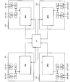
- a signal distribution unit (inter-substrate connection unit) CF is provided between the display control substrates DC1 to DC4.
- the inter-substrate signal sharing circuits SHB1 to SHB4 and the signal distribution unit CF are a pair for transmitting differential signals (inter-board fail-safe signals) from the inter-substrate signal sharing circuits SHB1 to SHB4 to the signal distribution unit CF.
- the inter-substrate signal line is connected to the inter-substrate signal sharing circuits SHB1 to SHB4 from the signal distribution unit CF by a pair of inter-substrate signal lines for transmitting a differential signal (inter-board fail-safe signal) ( In FIG. 9, each line is omitted by a single line). These inter-substrate signal lines transmit signals only in one direction.
- the signal distribution unit CF may be mounted on any one of the display control boards DC1 to DC4.
- the timing controller TC1, timing controller TC2, and inter-board signal sharing circuit SHB1 mounted on the same display control board DC1 are connected by wired-or connection using a single-end in-board signal line.
- the timing controller TC1, the timing controller TC2, and the inter-substrate signal sharing circuit SHB1 transmit and receive an in-board fail-safe signal through the in-board signal line.
- the in-board fail-safe signal is DISABLE (invalid), that is, the voltage of the in-board signal line is maintained at the H level.
- timing controllers TC1 and TC2 The operation of the timing controllers TC1 and TC2 is the same as that of the first embodiment.
- the inter-board signal sharing circuit SHB1 when the in-board fail safe signal is DISABLE (invalid) (H level), the inter-board signal sharing circuit SHB1 outputs the inter-board fail safe signal to the signal distribution unit CF. (L level).
- the inter-board signal sharing circuit SHB1 when the in-board fail-safe signal is ENABLE (valid) (L level), the inter-board signal sharing circuit SHB1 is connected to one end of the inter-board signal line (not shown). ), The inter-board fail-safe signal ENABLE (effective) (H level) is output to the signal distribution unit CF.
- the inter-board signal sharing circuit SHB1 detects that the inter-board fail safe signal from the signal distribution unit CF is ENABLE (valid) (H level)
- the inter-substrate signal sharing circuit SHB1 The port is set as an output port, and the in-board fail-safe signal ENABLE (valid) (L level) is output to the timing controllers TC1 and TC2.
- the signal distribution unit CF monitors the ENABLE (valid) / DISABLE (invalid) of the inter-board fail-safe signals from the inter-board signal sharing circuits SHB1 to SHB4. When the inter-board fail sharing signals from all the inter-board signal sharing circuits SHB1 to SHB4 are DISABLE (invalid), the signal distribution unit CF outputs the inter-board fail safe signals to the inter-board signal sharing circuits SHB1 to SHB4. (To disable.
- the signal distribution unit CF detects that the inter-board fail-safe signal from one inter-board signal sharing circuit SHB1 is ENABLE (valid) (H level), for example, the other inter-substrate signal sharing circuits SHB2 to The inter-board fail safe signal ENABLE (valid) (H level) is output to SHB4. At this time, the signal distribution unit CF makes the inter-board fail safe signal DISABLE (invalid) for the inter-board signal sharing circuit SHB1 outputting the inter-board fail safe signal ENABLE (valid) to the signal distribution unit CF.
- the display control board that outputs the inter-board fail-safe signal ENABLE (valid) to the signal distribution unit CF
- one of the timing controllers is in an abnormal state, and the in-board fail-safe signal is already ENABLE (valid). This is because the timing controller has shifted to the self-running mode.
- the inter-board fail-safe signal ENABLE (valid) is input to the signal distribution unit CF from a plurality of inter-board signal sharing circuits, the signal distribution unit CF is inter-substrate only for the other inter-board signal sharing circuits. Outputs a fail-safe signal ENABLE (valid).
- the in-board fail-safe signal becomes DISABLE (invalid)
- the corresponding inter-board signal sharing circuit of the display control board becomes the inter-board fail safe to the signal distribution unit CF.
- the signal distribution unit CF outputs inter-board fail-safe signals to be output to the inter-board signal sharing circuits SHB1 to SHB4 to DISABLE ( To disable.
- each inter-board signal sharing circuit and the signal distribution unit are configured as a single unit.
- the board-to-board signal line may be connected to transmit a board-to-board fail-safe signal.
- the signal distribution unit obtains the AND result of a plurality of inter-board fail-safe signals input from the inter-board signal sharing circuit.
- the signal may be output as an inter-board fail-safe signal to each inter-board signal sharing circuit.
- the signal distribution unit when an abnormal state has occurred in any of the display control boards, the signal distribution unit outputs the inter-board fail safe signal ENABLE (valid) to all the inter-board signal sharing circuits. Therefore, in order to return from the self-running mode, the signal distribution unit may once disable DISABLE (interval) the inter-board fail-safe signals to all the inter-board signal sharing circuits every predetermined period. As a result, if all timing controllers are recovered from the abnormal state, all inter-board fail-safe signals and in-board fail-safe signals become DISABLE (invalid), and all timing controllers operate normally from the free-running mode. Return to mode.
- a display device includes a display portion including a first region and a second region, a first substrate provided with a first timing controller that performs display control of the first region, and the second region.
- a second substrate provided with a second timing controller for performing display control, and an inter-substrate connecting portion for connecting the first substrate and the second substrate, wherein the first timing controller includes the first region.
- the 1st timing controller and the 2nd timing controller can perform suitable treatment (for example, self-running control) to the above-mentioned abnormality.
- the second timing controller transmits a fail-safe signal to the inter-board connection portion, and the first timing controller indicates that the abnormality has occurred. It may be configured to communicate to.
- the first timing controller sets the display control of the first area to the fail-safe mode, and the abnormality occurs in the first timing controller.
- the second timing controller may be configured to set the display control of the second area to the fail-safe mode.
- the display device is mounted on the first substrate, and is mounted on the first substrate, the first interface unit connected to the first timing controller and the inter-substrate connection unit, and the second timing controller and A second interface unit connected to the inter-board connection unit, and when the first interface unit receives an in-board fail-safe signal from the first timing controller, the differential signal is transmitted via the inter-board connection unit.
- the inter-board fail-safe signal is transmitted from the second interface unit to the second interface unit via the inter-board connection unit, the inter-board fail-safe signal is transmitted to the first timing controller.
- An internal fail-safe signal is transmitted, and the second interface unit is When the in-board fail-safe signal is received from the second timing controller, the inter-board fail-safe signal is transmitted to the first interface unit using the differential signal via the inter-board connection unit, and the inter-board connection is performed. When the inter-board fail-safe signal is received from the first interface unit via the unit, the intra-board fail-safe signal may be transmitted to the second timing controller.
- the first interface unit has a first differential signal transmission / reception having an output mode for outputting an inter-board fail-safe signal to the inter-board connection unit and an input mode for monitoring the inter-board fail-safe signal of the inter-board connection unit. And a first input / output switching unit that switches the output mode and the input mode of the first differential signal transmitting / receiving unit, and the second interface unit outputs an inter-board fail-safe signal to the inter-board connecting unit. And a second differential signal transmitting / receiving unit having an input mode for monitoring an inter-board fail-safe signal of the inter-board connection unit, and a second switching between the output mode and the input mode of the second differential signal transmitting / receiving unit.
- An input / output switching unit wherein the first input / output switching unit is configured such that the first differential signal transmitting / receiving unit transmits the second differential signal via the inter-substrate connection unit.
- the in-board fail-safe signal is transmitted to the first timing controller, and when the in-board fail-safe signal is received from the first timing controller, the first differential signal is transmitted.
- the transmission / reception unit is switched from the input mode to the output mode, and the second input / output switching unit is configured such that the second differential signal transmission / reception unit fails from the first differential signal transmission / reception unit via the inter-board connection unit.
- the in-board fail-safe signal is transmitted to the second timing controller, and when the in-board fail-safe signal is received from the second timing controller, the second differential signal transmitting / receiving unit is set to the input mode. May be configured to switch to the output mode.
- the first input / output switching unit includes a first differential signal output unit and a first differential signal input unit that are multi-point connected, and the first input / output switching unit is configured to perform the above operation according to an in-board fail-safe signal from the first timing controller. Which one of the first differential signal output unit and the first differential signal input unit is activated is switched, and the second input / output switching unit includes a second differential signal output unit and a second multipoint-connected second differential signal output unit.
- the display device includes three or more substrates including the first substrate and the second substrate, and three or more timings including the first timing controller and the second timing controller mounted on each substrate.
- the inter-substrate connection portion connects the three or more interface portions in a ring shape, and each interface portion is connected to the substrate from another interface portion via the inter-substrate connection portion.
- inter-board fail-safe signal When transmitting an inter-board fail-safe signal to another interface unit via the inter-board connection unit, and receiving an in-board fail-safe signal from the timing controller of the mounted board, The inter-board fail-safe signal is transmitted to the further interface unit via the inter-board connection unit, and each timing controller is configured to display the board when an abnormality occurs in display control of the corresponding area.
- the configuration may be such that a fail safe signal is transmitted to the inter-connection portion, and the fact that the abnormality has occurred is transmitted to the other timing controllers.
- the display device includes three or more substrates including the first substrate and the second substrate, and three or more timings including the first timing controller and the second timing controller mounted on each substrate.
- Each interface unit includes a signal distribution unit, and when each interface unit receives the in-board fail-safe signal from the timing controller of the mounted board, the inter-board fail-safe signal is transmitted to the signal distribution unit, and the signal distribution When the board-to-board fail-safe signal is received from the When the inter-board fail-safe signal is received from at least one of the plurality of interface units, the signal distribution unit transmits the inter-board fail-safe signal to the operating controller.
- An inter-board fail-safe signal may be transmitted to the other interface unit that is not.
- the signal distribution unit may transmit the inter-board fail-safe signal to all the interface units when receiving the inter-board fail-safe signal from at least one of the plurality of interface units.
- inter-board fail safe signal may be a differential signal.
- timing controller and the interface unit mounted on the same board are connected to each other by a single-ended signal line that is wired or connected, and can transmit and receive an in-board fail-safe signal bidirectionally. It may be a configuration.
- the present invention can be used for a large screen display type display device.
Landscapes
- Engineering & Computer Science (AREA)
- Chemical & Material Sciences (AREA)
- Crystallography & Structural Chemistry (AREA)
- Physics & Mathematics (AREA)
- Computer Hardware Design (AREA)
- General Physics & Mathematics (AREA)
- Theoretical Computer Science (AREA)
- Power Engineering (AREA)
- Control Of Indicators Other Than Cathode Ray Tubes (AREA)
Abstract
本発明の一態様に係る液晶表示装置は、表示部と、部分表示領域(AR1)の表示制御を行うタイミングコントローラ(TC1)が設けられた表示制御基板(DC1)と、部分表示領域(AR3)の表示制御を行うタイミングコントローラ(TC3)が設けられた表示制御基板(DC2)と、表示制御基板(DC1)と表示制御基板(DC2)とを接続する基板間接続部とを備え、タイミングコントローラ(TC1)は、部分表示領域(AR1)の表示制御に異常が生じた場合には、基板間接続部にフェイルセーフ信号を送信する。
Description
本発明は、複数のタイミングコントローラが搭載された表示装置に関する。
液晶表示装置の高精細化に伴う各画素への書き込み時間の短縮、および液晶表示装置の大型化に伴う信号波形の鈍りに対応するため、表示画面を複数の部分表示領域に分割し、各部分表示領域を別々に駆動する構成(画面分割方式)が提案されている(例えば特許文献1~3参照)。この画面分割方式では、例えば、1画面を上下分割し(上側領域を第1領域、下側領域を第2領域とする)、第1領域にはフレームの前半(上側)を表示し、第2領域には該フレームの後半(下側)を表示する。
また、高精細な映像規格として、フルHD(Full High Definition)(1920×1080画素の解像度)の4倍(縦2倍×横2倍)の画素数を有するQFHD(Quad Full High Definition)(通称4K2K)、および、フルHDの16倍(縦4倍×横4倍)の画素数を有するSHV(Super Hi-Vision、またはUHDTV:Ultra High Definition Television)(通称8K4K)の規格が提案されている。
これらの超高精細(4K2K解像度または8K4K解像度)の映像信号を表示する場合、処理しなければならない信号の量が大量になるので、現状では画面分割方式によって表示せざるを得ない。また、例えば8K4K解像度の映像信号を表示させる場合、その画素数のために表示パネル自体も大型になる。また、大量の映像信号を処理するため、表示を制御するタイミングコントローラも複数設ける必要が出てくる。
しかしながら、タイミングコントローラの映像信号の出力の準備が、何らかの原因により、正常に行われない場合、そのタイミングコントローラに対応する部分表示領域にだけ画像が表示されないといったことが起こりうる。例えば、タイミングコントローラ自身の動作に異常が発生した、電源起動時に、タイミングコントローラの前段のデバイスが未だ起動しておらず映像信号が入力されていない、または、前段のいずれかのデバイスの動作に異常が発生した、または、表示装置に入力された映像信号自体が不適切なものである等の原因により、タイミングコントローラに入力された映像信号のタイミングが適正なものではないことが考えられる。ここで映像信号のタイミングが適正ではないとは、例えば、水平同期信号のSync幅、フロントポーチ幅、バックポーチ幅、有効期間、または垂直同期信号のSync幅、フロントポーチ幅、バックポーチ幅、有効期間、あるいはDataEnable信号等が適正ではないことを指す。また、あるタイミングコントローラに入力される映像信号のタイミングが適正ではない場合、対応する部分表示領域の表示が破綻する可能性がある。そのため、一部の表示が正常ではない状態で画像の表示を行うよりも、表示領域全体の映像の表示を行わない(例えば黒表示にする)方が好ましい。
よって、いずれかのタイミングコントローラで異常が発生した場合(映像信号のタイミングが正常なものではない場合)、表示領域全体の表示を同様の状態に制御することが考えられる。
本発明は、上記の問題点に鑑みてなされたものであり、その目的は、複数のタイミングコントローラによって映像データの並列処理を行う表示装置において、いずれかのタイミングコントローラで異常が発生した場合に、不適切な表示を防止することができる表示装置を実現することにある。
本発明に係る表示装置は、第1領域および第2領域を含む表示部と、上記第1領域の表示制御を行う第1タイミングコントローラが設けられた第1基板と、上記第2領域の表示制御を行う第2タイミングコントローラが設けられた第2基板と、上記第1基板と上記第2基板とを接続する基板間接続部とを備え、上記第1タイミングコントローラは、上記第1領域の表示制御に異常が生じた場合には、上記基板間接続部にフェイルセーフ信号を送信し、上記異常が発生したことを上記第2タイミングコントローラに伝えることを特徴としている。
上記の構成によれば、第1基板に設けられた第1タイミングコントローラの表示制御に異常が発生したことを、別の第2基板に設けられた第2タイミングコントローラに伝えることができる。これにより、第1タイミングコントローラおよび第2タイミングコントローラは、上記異常に対して適切な処置(例えば自走制御)を行うことができる。
以上のように、第1基板に設けられた第1タイミングコントローラの表示制御に異常が発生したことを、別の第2基板に設けられた第2タイミングコントローラに伝えることができる。これにより、第1タイミングコントローラおよび第2タイミングコントローラは、上記異常に対して適切な処置(例えば自走制御)を行うことができる。
[実施形態1]
以下、本発明の一実施形態について、図1~図7に基づいて説明する。
以下、本発明の一実施形態について、図1~図7に基づいて説明する。
<液晶表示装置の全体構成>
本実施形態に係る液晶表示装置LCDは、フルHD画素数の16倍の画素数(8K4K)を有する映像規格(例えば、横7680画素×縦4320画素の解像度を有するスーパーハイビジョン)に対応するものであり、図2に示すように、入力処理回路IPC、ピクセルマッピング回路PMC、4つの表示制御基板(タイミングコントローラ基板)DC1~DC4、液晶パネル(表示部)LCP、4つのゲートドライバGD1~GD4、2つのソースドライバSD1~SD2、4つのCSドライバCD1~CD4、それぞれが異なる商用電源に接続される3つの電源装置(図示せず)、電源コントローラ(図示せず)、バックライトBL、バックライトドライバBLD、およびバックライトコントローラBLCを備える。
本実施形態に係る液晶表示装置LCDは、フルHD画素数の16倍の画素数(8K4K)を有する映像規格(例えば、横7680画素×縦4320画素の解像度を有するスーパーハイビジョン)に対応するものであり、図2に示すように、入力処理回路IPC、ピクセルマッピング回路PMC、4つの表示制御基板(タイミングコントローラ基板)DC1~DC4、液晶パネル(表示部)LCP、4つのゲートドライバGD1~GD4、2つのソースドライバSD1~SD2、4つのCSドライバCD1~CD4、それぞれが異なる商用電源に接続される3つの電源装置(図示せず)、電源コントローラ(図示せず)、バックライトBL、バックライトドライバBLD、およびバックライトコントローラBLCを備える。
入力処理回路IPCに入力される映像信号は、ブロックスキャンフォーマットの8K4K画素数を有する映像信号(例えば、スーパーハイビジョン)であってもよいし、マルチディスプレイフォーマットの8K4K画素数を有する映像信号であってもよい。もちろん、4K2K画素数を有する映像信号であってもよいし、2K1K画素数(フルHD画素数)を有する映像信号であってもよい。
ブロックスキャンフォーマットは、1フレーム(8K4K画素数を有する全体画像)をキメの粗い(フルHD画素数の)16枚の全体画像(いわゆる間引き画像)に分割して送信する方式である。この場合、入力処理回路IPCに入力される16本の映像信号Qa1~Qa16それぞれが、キメの粗い全体画像(フルHD画素数)となっている。
マルチディスプレイフォーマットは、1フレーム(8K4K画素数を有する全体画像)をキメの細かさを変えることなく16分割し、16枚の部分画像に分割して送信する方式である。この場合、入力処理回路IPCに入力される16本の映像信号Qa1~Qa16それぞれが、キメの細かい部分画像(フルHD画素数)となっている。
入力処理回路IPCでは、映像データの同期処理、γ補正処理、色温度補正処理、および色域変換処理等を行い、映像信号Qb1~Qb16をピクセルマッピング回路PMCに出力する。
ここで、表示制御基板DC1は、2つの映像処理回路EP1・EP2および2つのタイミングコントローラTC1・TC2を備え、表示制御基板DC2は、2つの映像処理回路EP3・EP4および2つのタイミングコントローラTC3・TC4を備え、表示制御基板DC3は、2つの映像処理回路EP5・EP6および2つのタイミングコントローラTC5・TC6を備え、表示制御基板DC4は、2つの映像処理回路EP7・EP8および2つのタイミングコントローラTC7・TC8を備える。
ピクセルマッピング回路PMCは、第1領域(液晶パネルLCPを上下左右に4分割したときの左上領域)の左半分AR1に対応する映像信号(画素数2K2K)を、2本(フルHD画素数の映像信号Qc1・Qc2)に分割して表示制御基板DC1の映像処理回路EP1に出力し、上記第1領域の右半分AR2に対応する映像信号(画素数2K2K)を、2本(フルHD画素数の映像信号Qc3・Qc4)に分割して表示制御基板DC1の映像処理回路EP2に出力し、第2領域(液晶パネルLCPを上下左右に4分割したときの右上領域)の左半分AR3に対応する映像信号(画素数2K2K)を、2本(フルHD画素数の映像信号Qc5・Qc6)に分割して表示制御基板DC2の映像処理回路EP3に出力し、上記第2領域の右半分AR4に対応する映像信号(画素数2K2K)を、2本(フルHD画素数の映像信号Qc7・Qc8)に分割して表示制御基板DC2の映像処理回路EP4に出力し、第3領域(液晶パネルLCPを上下左右に4分割したときの左下領域)の左半分AR5に対応する映像信号(画素数2K2K)を、2本(フルHD画素数の映像信号Qc9・Qc10)に分割して表示制御基板DC3の映像処理回路EP5に出力し、上記第3領域の右半分AR6に対応する映像信号(画素数2K2K)を、2本(フルHD画素数の映像信号Qc11・Qc12)に分割して表示制御基板DC3の映像処理回路EP6に出力し、第4領域(液晶パネルLCPを上下左右に4分割したときの右下領域)の左半分AR7に対応する映像信号(画素数2K2K)を、2本(フルHD画素数の映像信号Qc13・Qc14)に分割して表示制御基板DC4の映像処理回路EP7に出力し、上記第4領域の右半分AR8に対応する映像信号(画素数2K2K)を、2本(フルHD画素数の映像信号Qc15・Qc16)に分割して表示制御基板DC4の映像処理回路EP8に出力する。
さらに、ピクセルマッピング回路PMCは、表示制御基板DC1のタイミングコントローラTC1に同期信号SYS(垂直同期信号、水平同期信号、クロック信号、データイネーブル信号、極性反転信号等)を出力し、これを受けたタイミングコントローラTC1は、この同期信号SYSを、表示制御基板DC1~DC4に接続された基板間共有線SSLに送信する。
タイミングコントローラTC1は、ピクセルマッピング回路PMCから受けた同期信号SYSを受けて映像処理回路EP1と協働し、映像信号Qc1・Qc2に階調変換処理およびフレームレート変換(FRC)処理等の映像処理を行った後に、AR1に対応するソースドライバ基板(図示せず)にソース制御信号SC1を出力し、ゲートドライバGD1のゲートドライバ基板(図示せず)にゲート制御信号GC1を出力し、CSドライバCD1にCS制御信号CC1を出力する。
タイミングコントローラTC2は、タイミングコントローラTC1から基板間共有線SSLを介して送信された同期信号SYSを受けて映像処理回路EP2と協働し、映像信号Qc3・Qc4に上記映像処理を行った後に、AR2に対応するソースドライバ基板(図示せず)にソース制御信号SC2を出力する。
タイミングコントローラTC3は、タイミングコントローラTC1から基板間共有線SSLを介して送信された同期信号SYSを受けて映像処理回路EP3と協働し、映像信号Qc5・Qc6に上記映像処理を行った後に、AR3に対応するソースドライバ基板(図示せず)にソース制御信号SC3を出力する。
タイミングコントローラTC4は、タイミングコントローラTC1から基板間共有線SSLを介して送信された同期信号SYSを受けて映像処理回路EP4と協働し、映像信号Qc7・Qc8に上記映像処理を行った後に、AR4に対応するソースドライバ基板(図示せず)にソース制御信号SC4を出力し、ゲートドライバGD2のゲートドライバ基板(図示せず)にゲート制御信号GC2を出力し、CSドライバCD2にCS制御信号CC2を出力する。
タイミングコントローラTC5は、タイミングコントローラTC1から基板間共有線SSLを介して送信された同期信号SYSを受けて映像処理回路EP5と協働し、映像信号Qc9・Qc10に上記映像処理を行った後に、AR5に対応するソースドライバ基板(図示せず)にソース制御信号SC5を出力し、ゲートドライバGD3のゲートドライバ基板(図示せず)にゲート制御信号GC3を出力し、CSドライバCD3にCS制御信号CC3を出力する。
タイミングコントローラTC6は、タイミングコントローラTC1から基板間共有線SSLを介して送信された同期信号SYSを受けて映像処理回路EP6と協働し、映像信号Qc11・Qc12に上記映像処理を行った後に、AR6に対応するソースドライバ基板(図示せず)にソース制御信号SC6を出力する。
タイミングコントローラTC7は、タイミングコントローラTC1から基板間共有線SSLを介して送信された同期信号SYSを受けて映像処理回路EP7と協働し、映像信号Qc13・Qc14に上記映像処理を行った後に、AR7に対応するソースドライバ基板(図示せず)にソース制御信号SC7を出力する。
タイミングコントローラTC8は、タイミングコントローラTC1から基板間共有線SSLを介して送信された同期信号SYSを受けて映像処理回路EP8と協働し、映像信号Qc15・Qc16に上記映像処理を行った後に、AR8に対応するソースドライバ基板(図示せず)にソース制御信号SC8を出力し、ゲートドライバGD4のゲートドライバ基板(図示せず)にゲート制御信号GC4を出力し、CSドライバCD4にCS制御信号CC4を出力する。
なお、ソース制御信号SC1~SC8には、データ信号、データイネーブル信号(DE信号)、ソーススタートパルス、およびソースクロックが含まれ、ゲート制御信号GC1~GC4には、イニシャル信号、ゲートスタートパルスおよびゲートクロックが含まれる。
また、表示制御基板DC1~DC4の動作中にいずれかの表示制御基板に異常が発生した場合には、異常が発生した表示制御基板から送信されたフェイルセーフ信号が、他のすべての表示制御基板で受信され、全ての表示制御基板は瞬時に自走(黒表示)モードとなる。これにより、映像破綻が回避される。
液晶パネルLCPは、アクティブマトリクス基板、液晶層(図示せず)および対向基板(図示せず)を備え、アクティブマトリクス基板には、複数の画素電極(図示せず)、複数のTFT(薄膜トランジスタ、図示せず)、行方向(パネルの長辺に沿う方向)に延伸する走査信号線Ga~Gd、列方向に延伸する複数のデータ信号線Sa~Sd、行方向に延伸する保持容量配線(CS配線)CSa~CSd、および列方向に延伸するCS幹配線Ma~Mhが設けられ、対向基板には、共通電極(図示せず)、カラーフィルタ、およびブラックマトリクス(図示せず)が設けられている。
液晶パネルLCPは、1つの画素列の上半分(パネルの上流側)に対応して2本のデータ信号線が設けられるとともに、この画素列の下半分(パネルの下流側)に対応して2本のデータ信号線が設けられた、いわゆる上下分割ダブルソース構造(1画素列あたり4本のデータ信号線が設けられ、同時に4本の走査信号線を選択することが可能な構造)を有し、4倍速駆動が可能である。さらに、液晶パネルLCPは、1つの画素に少なくとも2つの画素電極を備えたいわゆるマルチ画素方式であり、1画素内に形成された明領域と暗領域とによって視野角特性を高めることが可能となっている。
例えば、図2および図3に示すように、パネルの上半分(上流側)に走査信号線Ga・Gbおよび保持容量配線CSa・CSbが設けられるとともに、パネルの下半分(下流側)に走査信号線Gc・Gdおよび保持容量配線CSc・CSdが設けられ、1つの画素列PL1の上半分(上流側)に列方向に隣り合う2つの画素Pa・Pbが含まれるともに、画素列PL1の下半分(下流側)に列方向に隣り合う2つの画素Pc・Pdが含まれ、画素列PL1の上半分(上流側)に対応してデータ信号線Sa・Sbが設けられるとともに、画素列PL1の下半分(下流側)に対応してデータ信号線Sc・Sdが設けられている。
そして、画素Paに含まれる2つの画素電極17A・17aのうち画素電極17Aに接続するTFT12Aおよび画素電極17aに接続するTFT12aそれぞれが、データ信号線Saと走査信号線Gaとに接続され、画素電極17Aが保持容量配線と保持容量を形成し、画素電極17aが保持容量配線CSaと保持容量を形成し、さらに、画素Pbに含まれる2つの画素電極17B・17bのうち画素電極17Bに接続するTFT12Bおよび画素電極17bに接続するTFT12bそれぞれが、データ信号線Sbと走査信号線Gbとに接続され、画素電極17Bが保持容量配線CSaと保持容量を形成し、画素電極17bが保持容量配線CSbと保持容量を形成し、さらに、画素Pcに含まれる2つの画素電極17C・17cのうち画素電極17Cに接続するTFT12Cおよび画素電極17cに接続するTFT12cそれぞれが、データ信号線Scと走査信号線Gcとに接続され、画素電極17Cが保持容量配線と保持容量を形成し、画素電極17cが保持容量配線CScと保持容量を形成し、さらに、画素Pdに含まれる2つの画素電極17D・17dのうち画素電極17Dに接続するTFT12Dおよび画素電極17dに接続するTFT12dそれぞれが、データ信号線Sdと走査信号線Gdとに接続され、画素電極17Dが保持容量配線CScと保持容量を形成し、画素電極17dが保持容量配線CSdと保持容量を形成しており、4本の走査信号線Ga~Gdは同時に選択される。
なお、パネル上半分に設けられたデータ信号線の数は、少なくとも7680(画素)×3(原色)×2(ダブルソース)=46080本であり、パネル上半分に設けられた走査信号線の数は、少なくとも4320本であり、パネル上半分に設けられた保持容量配線の数は、少なくとも4321本であり、パネル下半分に設けられたデータ信号線の数は、少なくとも46080本であり、パネル下半分に設けられた走査信号線の数は、少なくとも4320本であり、パネル下半分に設けられた保持容量配線の数は、少なくとも4320本である。
また、同時に選択される4本の走査信号線Ga~Gdについて、走査信号線Gaがパネルの上側長辺から数えてMライン目で走査信号線GbがM+1ライン目とすると、走査信号線Gcは、この上側長辺から数えてM+2160ライン目で走査信号線GbがM+2161ライン目となっており、パネル上半分に設けられた走査信号線Gaに第NフレームのMライン目のデータ信号が書き込まれるとすると、パネル下半分に設けられた走査信号線Gcには、1つ前のフレームである第N-1フレームのM+2160ライン目のデータ信号が書き込まれる。
また、1つのデータ信号線の供給されるデータ信号の極性は1垂直走査期間(1V)ごとに反転し、同一垂直走査期間では、隣り合う2つのデータ信号線の一方と他方とに供給されるデータ信号の極性が逆極性となっている。こうすれば、各データ信号線を1V反転としながら(すなわち、極性反転周期を長くして消費電力を低減しながら)、画面内の画素の極性分布をドット反転とする(これにより、TFTがOFFしたときに生じる引き込み電圧に起因するフリッカを抑制する)ことができる。
また、ゲートドライバGD1は、液晶パネルLCPの上半分が有する2つの短辺の一方に沿って設けられ、列方向に並ぶ複数のゲートドライバチップIを含む。垂直ドライバGD2は、液晶パネルLCPの上半分が有する上記2つの短辺の他方に沿って設けられ、列方向に並ぶ複数のゲートドライバチップIを含む。また、ゲートドライバGD3は、液晶パネルLCPの下半分が有する2つの短辺の一方に沿って設けられ、列方向に並ぶ複数のゲートドライバチップIを含む。垂直ドライバGD4は、液晶パネルLCPの下半分が有する上記2つの短辺の他方に沿って設けられ、列方向に並ぶ複数のゲートドライバチップIを含む。そして、パネル上半分に設けられた各走査信号線はゲートドライバGD1・GD2によって駆動され、パネル下半分に設けられた各走査信号線はゲートドライバGD3・GD4によって駆動される。すなわち、1本の走査信号線がその両側に配置された2つのゲートドライバに接続され、これら2つのゲートドライバからこの1つの走査信号線に同一位相の走査(パルス)信号が供給される。こうすれば、走査信号線のCR(時定数)に起因する信号鈍りのばらつき(行方向の位置によって信号鈍りの度合いが変わること)を抑制することができる。
ソースドライバSD1は、液晶パネルLCPの上半分が有する1つの長辺に沿って設けられ、行方向に並ぶ48個のソースドライバチップJ(1つのソースドライバチップの出力端子数は960個)と、図示しない4つのソースドライバ基板を含む(1つのソースドライバ基板には12個のソースドライバチップJが装着される)。一方、ソースドライバSD2は、液晶パネルLCPの下半分が有する1つの長辺に沿って設けられ、行方向に並ぶ48個のソースドライバチップJ(1つのソースドライバチップの出力端子数は960個)と、図示しない4つのソースドライバ基板を含む(1つのソースドライバ基板には12個のソースドライバチップJが装着される)。そして、パネル上半分に設けられた各データ信号線はソースドライバSD1によって駆動され、パネル下半分に設けられた各データ信号線はソースドライバSD2によって駆動される。例えば、データ信号線SaはソースドライバSD1によって駆動され、データ信号線ScはソースドライバSD2によって駆動される。なお、スペースの関係でソースドライバチップJをパネル長辺に沿って並べることができない場合は、スペースの余裕のあるパネル短辺側に並べる(ソースドライバチップJとゲートドライバチップIとを列方に並べる)こともできる。この場合、データ信号線とパネル短辺側のソース端子とを接続する中継ラインを、対向基板側に設けたり、アクティブマトリクス基板のソース層(TFTのソース・ドレイン電極の形成層)以外、すなわち、ゲート絶縁膜の下層(ゲート層)やソース層とITO層(画素電極形成層)との間の層に設けたりすることもできる。
CS幹配線Ma・Mbは、アクティブマトリクス基板の上半分が有する2つの短辺の一方に近接して設けられ、CSドライバCD1によってそれぞれが別位相となるように駆動される。CS幹配線Mc・Mdは、アクティブマトリクス基板の上半分が有する上記2つの短辺の他方に近接して設けられ、CSドライバCD2によってそれぞれが別位相となるように駆動される。CS幹配線Me・Mfは、アクティブマトリクス基板の下半分が有する2つの短辺の一方に近接して設けられ、CSドライバCD3によってそれぞれが別位相となるように駆動される。CS幹配線Mg・Mhは、アクティブマトリクス基板の下半分が有する上記2つの短辺の他方に近接して設けられ、それぞれが別位相となるようにCSドライバCD4によって駆動される。そして、1本の保持容量配線は、その両側に配置された2本のCS幹配線に接続され、これら2本のCS幹配線からこの1本の保持容量配線に同一位相の変調(パルス)信号が供給される。こうすれば、保持容量配線のCR(時定数)に起因する信号鈍りのばらつき(行方向の位置によって信号鈍りの度合いが変わること)を抑制することができる。
例えば、保持容量配線CSaはCS幹配線Ma・Mcに接続され、保持容量配線CSbはCS幹配線Mb・Mdに接続され、保持容量配線CScはCS幹配線Me・Mgに接続され、保持容量配線CSdはCS幹配線Mf・Mhに接続されている。したがって、例えば、CS幹配線Ma・Mbの電位を逆位相となるように制御すると、保持容量配線CSa・CSbの電位も逆位相となり、画素Pbでは、2つの画素電極17B・17bのうち画素電極17Bが保持容量配線CSaと容量を形成し、画素電極17bが保持容量配線CSbと容量を形成していることから、画素電極17B・17bに同一の信号電位を書き込んだ後に、例えば、画素電極17Bの実効電位をセンター電位に近づく方向にシフトさせる一方、画素電極17bの実効電位をセンター電位から離れる方向にシフトさせる(これにより、1画素内に、画素電極17Bに対応する暗領域と画素電極17bに対応する明領域とを形成する)ことができる。
4つの表示制御基板DC1~DC4は、それぞれ8つの部分表示領域AR1~AR8のうちの2つの部分表示領域に対応する映像データを並列に処理している。そして、各表示制御基板DC1~DC4は、互いに異なる部分表示領域AR1~AR8の表示を制御している。
そのため、いずれかの表示制御基板で映像データの異常(映像信号のタイミングの異常)が発生したとき、表示領域全体を自走(黒表示)モードにして表示領域全体の表示を適切に制御するためには、異常の情報を表示制御基板DC1~DC4の間で共有する必要がある。また、表示領域全体の表示を同時に制御(黒表示等)するために、異常の情報の共有には、即時性が求められる。
異常の情報を共有する方法として、各タイミングコントローラTC1~TC8の間でフェイルセーフ信号を送受信することが考えられる。フェイルセーフ信号は、異常が発生したときにタイミングコントローラTC1~TC8が異常状態に応じた動作(自走制御)を行うための信号であり、あるタイミングコントローラが正常状態であるか異常状態であるかを他のタイミングコントローラに伝える信号である。いずれのタイミングコントローラTC1~TC8で異常が発生した場合でも、全てのタイミングコントローラTC1~TC8でその異常の情報を共有するために、双方向の通信が可能でなければならない。
例えば、フェイルセーフ信号を1つの基板に搭載された2つのタイミングコントローラの間でやりとりするためには、2つのタイミングコントローラをシングルエンドの信号線を用いてワイヤード・オア接続によって接続すればよい。そして、1つの基板に搭載された2つのタイミングコントローラの間でフェイルセーフ信号を送信および受信することで、異常の情報の共有をすることができる。複数のタイミングコントローラが1つの基板に搭載されている場合、基板内に近接して配置される複数のタイミングコントローラを構成する各ICチップを信号線で接続すればよい。
しかしながら、本実施形態のように複数のタイミングコントローラが異なる基板に搭載されている場合、該複数の基板が離れて位置していると、各タイミングコントローラを接続する(フェイルセーフ信号を送信する)信号線が基板の間に長く延びて配置されることになる。信号線が長くなると、外部ノイズの影響を受けやすくなるという問題が発生する。
本実施形態では、外部ノイズの影響を受けにくく、かつ、即時に異常情報を伝達可能な双方向通信を行う構成について説明する。
<表示制御基板の詳細な構成>
図1は、表示制御基板の詳細な構成を示すブロック図である。図1では、4つの表示制御基板DC1~DC4の構成のみを示し、他の構成部材の図示は省略している。また、タイミングコントローラTC1~TC8からの各表示制御基板外への出力の図示は省略している。
図1は、表示制御基板の詳細な構成を示すブロック図である。図1では、4つの表示制御基板DC1~DC4の構成のみを示し、他の構成部材の図示は省略している。また、タイミングコントローラTC1~TC8からの各表示制御基板外への出力の図示は省略している。
表示制御基板DC1は、2つの映像処理回路EP1・EP2、2つのタイミングコントローラTC1・TC2、および1つの基板間信号共有回路(インターフェース部)SH1を備える。表示制御基板DC2は、2つの映像処理回路EP3・EP4、2つのタイミングコントローラTC3・TC4、および1つの基板間信号共有回路SH2を備える。表示制御基板DC3は、2つの映像処理回路EP5・EP6、2つのタイミングコントローラTC5・TC6、および1つの基板間信号共有回路SH3を備える。表示制御基板DC4は、2つの映像処理回路EP7・EP8、2つのタイミングコントローラTC7・TC8、および1つの基板間信号共有回路SH4を備える。各表示制御基板DC1~DC4は、対応する部分表示領域AR1~AR8および対応するソースドライバチップJの位置に近接して配置されるため、互いに距離が離れている。
基板間信号共有回路SH1は、入出力切替部IFS1、LVDS(Low voltage differential signaling)ドライバ(差動信号出力部)LD1、およびLVDSレシーバ(差動信号入力部)LR1を備える。LVDSドライバLD1およびLVDSレシーバLR1は、セットで差動信号送受信部を構成している。基板間信号共有回路SH2は、入出力切替部IFS2、LVDSドライバLD2、およびLVDSレシーバLR2を備える。基板間信号共有回路SH3は、入出力切替部IFS3、LVDSドライバLD3、およびLVDSレシーバLR3を備える。基板間信号共有回路SH4は、入出力切替部IFS4、LVDSドライバLD4、およびLVDSレシーバLR4を備える。LVDSレシーバLR1~LR4は、Type-2仕様のマルチポイントLVDSである。Type-2仕様(フェイルセーフ機能付き)のマルチポイントLVDSレシーバは、High/Low判定の閾値を100mVオフセットさせたレシーバであり、電位差0Vの入力はLowに判定される。ただし、ここで言うType-2仕様のフェイルセーフ機能は、本発明のフェイルセーフ信号とは関係ない。
各LVDSドライバLD1~LD4および各LVDSレシーバLR1~LR4は、差動信号を伝送するための1対の基板間信号線(基板間接続部)に対して、マルチポイント接続されている。これにより、各基板間信号共有回路SH1~SH4が、互いに接続される。なお、各LVDSレシーバLR1~LR4のうち(バスの両端に位置する)2つのLVDSレシーバLR1・LR3付近の1対の基板間信号線の間には、終端抵抗が設けられている。なお、各LVDSドライバLD1~LD4には、出力に使用するための電圧として、常にHレベル(High)の電圧が入力されている。
映像処理回路EP1~EP8は、上述したようにそれぞれタイミングコントローラTC1~TC8と協働して、各種の映像処理を行う。
タイミングコントローラTC1は、あるフレームの映像信号Qc1・Qc2に対する上記映像処理が、所定のタイミング(所定の期間内)で完了するか否かを監視する。すなわちソース制御信号SC1、ゲート制御信号GC1、およびCS制御信号CC1を所定のタイミングで出力可能な状態になっている場合、タイミングコントローラTC1~TC8は、映像信号の入力および映像処理は正常に行われている状態(正常状態)であると判定する。正常状態では、各タイミングコントローラTC1~TC8から各ドライバに制御信号が遅延なく出力され、映像の表示が正常に行われる。
一方、ソース制御信号SC1、ゲート制御信号GC1、およびCS制御信号CC1のいずれかが所定のタイミングで出力可能な状態になっていない場合、タイミングコントローラTC1~TC8は、映像信号の入力または映像処理が正常に行われていない状態(異常状態)であると判定する。異常状態であるタイミングコントローラTC1~TC8は、正常なタイミングで制御信号を出力できない。よって、各部分表示領域AR1~AR8の表示を自走制御して映像の表示の破綻を防止するために、異常状態と判定したタイミングコントローラは、他のタイミングコントローラに異常状態を通知する必要がある。
(表示制御基板の動作)
以下では主に表示制御基板DC1のタイミングコントローラTC1・TC2および基板間信号共有回路SH1の動作について説明するが、他の表示制御基板DC2~DC4のタイミングコントローラTC3~TC8および基板間信号共有回路SH2~SH4についても同様である。
以下では主に表示制御基板DC1のタイミングコントローラTC1・TC2および基板間信号共有回路SH1の動作について説明するが、他の表示制御基板DC2~DC4のタイミングコントローラTC3~TC8および基板間信号共有回路SH2~SH4についても同様である。
同じ表示制御基板DC1に搭載されるタイミングコントローラTC1とタイミングコントローラTC2と基板間信号共有回路SH1とは、シングルエンドの基板内信号線を用いてワイヤード・オア接続によって接続されている。タイミングコントローラTC1とタイミングコントローラTC2と基板間信号共有回路SH1とは、基板内信号線を介して、基板内フェイルセーフ信号の送受信を行う。正常状態では、タイミングコントローラTC1・TC2および基板間信号共有回路SH1の基板内信号線に対する出力はOFFになっており、基板内フェイルセーフ信号はDISABLE(無効)になっている、すなわち基板内信号線の電圧はHレベルに維持されている。
自身が正常状態であると判定すると、タイミングコントローラTC1・TC2は、タイミングコントローラTC1・TC2の基板内信号線ポートを、入力ポートに設定する。これにより、タイミングコントローラTC1・TC2は、基板内フェイルセーフ信号のENABLE(有効)/DISABLE(無効)(基板内信号線の電圧レベル)を監視する。
自身が異常状態であると判定すると、タイミングコントローラTC1・TC2は、自走モードとなり、入力信号に依存せずに自身の内部で予め設定されたタイミングに従って自走制御のための制御信号を生成し、自走制御のための制御信号(ゲート制御信号および黒映像データ信号を含むソース制御信号等)を各ドライバに出力し、対応する部分表示領域AR1・AR2を黒表示にする。また、自身が異常状態であると判定すると、タイミングコントローラTC1・TC2は、タイミングコントローラTC1・TC2の基板内信号線ポートを、出力ポートに設定し、基板内フェイルセーフ信号をENABLE(有効)にする、すなわち基板内信号線の電圧をLレベル(Low)に駆動する。
また、自身が正常状態であっても、基板内フェイルセーフ信号がENABLE(有効)(基板内信号線の電圧がLレベル)であることを検知すると、タイミングコントローラTC1・TC2は、自走モードとなり、自走制御のための制御信号を各ドライバに出力し、対応する部分表示領域AR1・AR2を黒表示にする。
入出力切替部IFS1は、フェイルセーフ信号を、表示制御基板DC1の中のタイミングコントローラTC1・TC2から表示制御基板DC1の外のタイミングコントローラTC3~TC8に伝送するモードと、表示制御基板DC1の外のタイミングコントローラTC3~TC8から表示制御基板DC1の中のタイミングコントローラTC1・TC2に伝送するモードとを切り替える役割を果たす。
LVDSレシーバLR1から入出力切替部IFS1への入力信号がLレベルである場合(正常状態)、入出力切替部IFS1は、基板間信号共有回路SH1の基板内信号線側ポートを、入力ポートに設定し、基板間信号共有回路SH1の入出力切替部IFS1は、基板内フェイルセーフ信号のENABLE(有効)/DISABLE(無効)(基板内信号線の電圧レベル)を監視する。
基板内フェイルセーフ信号がDISABLE(無効)である場合、入出力切替部IFS1は、LVDSドライバLD1およびLVDSレシーバLR1に、ドライバ/レシーバの切り替えのための入出力制御信号(Lレベル)を出力する。また、基板内フェイルセーフ信号がENABLE(有効)である場合、入出力切替部IFS1は、LVDSドライバLD1およびLVDSレシーバLR1に、入出力制御信号(Hレベル)を出力する。
一方、LVDSレシーバLR1から入出力切替部IFS1への入力信号がHレベルである場合、入出力切替部IFS1は、基板間信号共有回路SH1の基板内信号線側ポートを、出力ポートに設定し、基板内フェイルセーフ信号をENABLE(有効)にする、すなわち基板内信号線の電圧をLレベルに駆動する。
入出力制御信号がLレベルである場合、LVDSドライバLD1は非アクティブとなり、LVDSレシーバLR1はアクティブとなる。すなわち、基板間信号共有回路SH1の基板間信号線側(LVDSドライバLD1およびLVDSレシーバLR1)は、入力モードに設定されている。よって、1対の基板間信号線の差動信号(基板間フェイルセーフ信号)は、M-LVDSタイプレシーバのType-2仕様におけるLレベル(DISABLE(無効):1対の基板間信号線の電位差が閾値より小さい)になっている。一方、入出力制御信号がHレベルである場合、LVDSドライバLD1はアクティブとなり、LVDSレシーバLR1は非アクティブとなる。このとき、基板間信号共有回路SH1の基板間信号線側は、出力モードに設定されている。よって、1対の基板間信号線の差動信号はHレベル(1対の基板間信号線の+極性の電位が-極性の電位より閾値以上高い、例えば図7(b)において、信号1(+極性)の電位が信号2(-極性)の電位より閾値以上高い)になっている。このとき、基板間フェイルセーフ信号はENABLE(有効)である。
入力モード時のLVDSレシーバLR1は、基板間フェイルセーフ信号を受信し、基板間フェイルセーフ信号に応じた信号を入出力切替部IFS1に出力する。すなわち、基板間フェイルセーフ信号がDISABLE(無効)(Lレベル)である場合、入力モード時のLVDSレシーバLR1は、Lレベルの信号を入出力切替部IFS1に出力する。基板間フェイルセーフ信号がENABLE(有効)(Hレベル)である場合、入力モード時のLVDSレシーバLR1は、Hレベルの信号を入出力切替部IFS1に出力する。
例えば、全てのタイミングコントローラTC1~TC8が正常状態であるときの、基板間信号共有回路SH1および基板間信号共有回路SH2の状態は、図4に示す表のようになる。このとき、基板間信号共有回路SH1・SH2について、基板内フェイルセーフ信号および基板間フェイルセーフ信号は共にDISABLE(無効)である。また、基板間信号共有回路SH1・SH2について、基板内信号線側ポートは入力ポートに設定されている。また、入出力切替部IFS1・IFS2が出力する入出力制御信号はLレベルであり、基板間信号線側(LVDSドライバLD1・LD2およびLVDSレシーバLR1・LR2)は入力モードに設定されている。
いずれかの表示制御基板に異常が発生した場合について説明する。
(タイミングコントローラTC1が異常状態である場合)
例えば、映像処理回路EP1の処理で異常が発生し、タイミングコントローラTC1に入力された映像信号が適切なものではなく、タイミングコントローラTC1が異常状態と判定したとする。このとき、タイミングコントローラTC1は、自身を自走モードに変更する。また、タイミングコントローラTC1は、タイミングコントローラTC1の基板内信号線ポートを、出力ポートに設定し、基板内フェイルセーフ信号をENABLE(有効)(Lレベル)に駆動する。タイミングコントローラTC2は、表示制御基板DC1の基板内フェイルセーフ信号がENABLE(有効)であることを検知すると、自身を自走モードに変更する。
例えば、映像処理回路EP1の処理で異常が発生し、タイミングコントローラTC1に入力された映像信号が適切なものではなく、タイミングコントローラTC1が異常状態と判定したとする。このとき、タイミングコントローラTC1は、自身を自走モードに変更する。また、タイミングコントローラTC1は、タイミングコントローラTC1の基板内信号線ポートを、出力ポートに設定し、基板内フェイルセーフ信号をENABLE(有効)(Lレベル)に駆動する。タイミングコントローラTC2は、表示制御基板DC1の基板内フェイルセーフ信号がENABLE(有効)であることを検知すると、自身を自走モードに変更する。
また、入出力切替部IFS1は、基板内フェイルセーフ信号がENABLE(有効)であることを検知すると、LVDSドライバLD1およびLVDSレシーバLR1に、入出力制御信号(Hレベル)を出力する。
Hレベルの入出力制御信号が入力されたLVDSドライバLD1はアクティブになり、LVDSレシーバLR1は非アクティブになる。すなわち、基板間信号共有回路SH1の基板間信号線側は、出力モードに設定される。LVDSドライバLD1は、基板間フェイルセーフ信号ENABLE(有効)(Hレベル)を出力する。
入力モードである表示制御基板DC2のLVDSレシーバLR2は、基板間フェイルセーフ信号がENABLE(有効)であることを検知し、Hレベルの信号を入出力切替部IFS2に出力する。
LVDSレシーバLR2からHレベルの信号を入力された入出力切替部IFS2は、基板間信号共有回路SH2の基板内信号線側ポートを、出力ポートに設定し、表示制御基板DC2の基板内フェイルセーフ信号をENABLE(有効)(Lレベル)に駆動する。
タイミングコントローラTC3・TC4は、表示制御基板DC2の基板内フェイルセーフ信号がENABLE(有効)であることを検知すると、自身を自走モードに変更する。
他の表示制御基板DC3・DC4においても、同様にタイミングコントローラTC5~TC8が自走モードに変更される。
このとき、基板間信号共有回路SH1および基板間信号共有回路SH2の状態は、図5に示す表のようになる。このとき、基板間信号共有回路SH1・SH2について、基板内フェイルセーフ信号および基板間フェイルセーフ信号は共にENABLE(有効)である。また、基板間信号共有回路SH1について、基板内信号線側ポートは入力ポートに設定されている。基板間信号共有回路SH2について、基板内信号線側ポートは出力ポートに設定されている。また、入出力切替部IFS1が出力する入出力制御信号はHレベルであり、基板間信号共有回路SH1の基板間信号線側(LVDSドライバLD1およびLVDSレシーバLR1)は出力モードに設定されている。また、入出力切替部IFS2が出力する入出力制御信号はLレベルであり、基板間信号共有回路SH2の基板間信号線側(LVDSドライバLD2およびLVDSレシーバLR2)は入力モードに設定されている。
なお、この自走モードは、異常状態が発生したタイミングコントローラTC1の異常状態が解消されない限り継続する。
以上により、ある表示制御基板DC1に搭載された1つのタイミングコントローラTC1で異常が発生した場合、フェイルセーフ信号が他の表示制御基板DC2~DC4に搭載されたものを含めた全てのタイミングコントローラTC2~TC8に即座に伝送される。それゆえ、即座に全タイミングコントローラTC1~TC8が自走モードに変更される。そのため、本実施形態では、一部の部分表示領域の表示と他の部分表示領域の表示とが整合していない不適切な表示を行うことを防止することができる。また、走査信号線Ga~Gdおよび保持容量配線(CS配線)CSa~CSdは、各部分表示領域AR1~AR8毎に分かれているわけではないので、ずれたタイミングで各タイミングコントローラTC1~TC8がゲートドライバGD1~GD4、ソースドライバSD1~SD2、およびCSドライバCD1~CD4に制御信号を出力すると、液晶パネルLCPを損傷する可能性がある。本実施形態によれば、一部のタイミングコントローラTC1~TC8が異常を検知すると、全てのタイミングコントローラTC1~TC8が自走モードで動作を行う。そのため、液晶パネルLCPの損傷を防止することができる。
また、異なる表示制御基板の間を差動信号によって基板間フェイルセーフ信号を伝送しているので、基板間信号線が長くても外部ノイズの影響を受けにくい。図7に、(a)一般的な不平衡信号と、(b)差動信号とを示す。不平衡信号(TTL、CMOS等)では、シングルエンドの1本の信号線によって信号を伝送し、信号線の電位とGND電位との差によって、HighおよびLowを表す。そのため、外部ノイズによって信号線の電位が変化すると、信号が誤って検出される可能性がある。差動信号(平衡信号、LVDS等)では、2本の信号線の電位の差によってHighおよびLowを表す。そのため、外部ノイズをキャンセルし、外部ノイズによる誤動作を防止することができる。
(タイミングコントローラTC1の異常状態が解消した場合)
タイミングコントローラTC1に異常状態が発生している図5に示す状態から、タイミングコントローラTC1の異常状態が解消した場合について以下に説明する。
タイミングコントローラTC1に異常状態が発生している図5に示す状態から、タイミングコントローラTC1の異常状態が解消した場合について以下に説明する。
タイミングコントローラTC1は、正常動作が可能になり異常状態が解消すると、自身の自走モードを通常の動作モードに変更する。また、タイミングコントローラTC1は、タイミングコントローラTC1の基板内信号線ポートを、入力ポートに設定し、基板内フェイルセーフ信号をDISABLE(無効)(Hレベル)にする。タイミングコントローラTC2は、表示制御基板DC1の基板内フェイルセーフ信号がDISABLE(無効)であることを検知すると、自身の自走モードを通常の動作モードに変更する。
入出力切替部IFS1は、表示制御基板DC1の基板内フェイルセーフ信号がDISABLE(無効)であることを検知すると、LVDSドライバLD1およびLVDSレシーバLR1に、入出力制御信号(Lレベル)を出力する。
Lレベルの入出力制御信号が入力されたLVDSドライバLD1は非アクティブになり、LVDSレシーバLR1がアクティブになる。すなわち、基板間信号共有回路SH1の基板間信号線側は、入力モードに設定される。これによりLVDSドライバLD1は非動作状態となり、基板間フェイルセーフ信号はDISABLE(無効)(Lレベル)に切り替わる。
入力モードである表示制御基板DC2のLVDSレシーバLR2は、基板間フェイルセーフ信号がDISABLE(無効)に切り替わったことを検知し、Lレベルの信号を入出力切替部IFS2に出力する。
LVDSレシーバLR2からLレベルの信号を入力された入出力切替部IFS2は、基板間信号共有回路SH2の基板内信号線側ポートを、入力ポートに設定し、表示制御基板DC2の基板内フェイルセーフ信号をDISABLE(無効)(Hレベル)に切り替える。
タイミングコントローラTC3・TC4は、表示制御基板DC2の基板内フェイルセーフ信号がDISABLE(無効)であることを検知すると、自身の自走モードを通常の動作モードに変更する。同様に他の表示制御基板DC3~DC4のタイミングコントローラTC5~TC8の自走モードも解除される。
以上により、全てのタイミングコントローラTC1~TC8の自走モードが解除され、通常の映像の表示が行われるようになる。異常状態が解消した場合の自走モードからの復帰も、異常状態の発生時と同様に、迅速に全てのタイミングコントローラTC1~TC8において行われる。よって、自走モードである期間を必要最小限に抑えることができる。
(タイミングコントローラTC1・TC3が異常状態である場合)
タイミングコントローラTC1に異常状態が発生している図5に示す状態から、さらに異なる表示制御基板DC2に搭載されるタイミングコントローラTC3にも異常状態が発生した場合について以下に説明する。なお、タイミングコントローラTC1・TC3においてほぼ同時に(TC1が少しだけ早く)異常状態が検知された場合もこれに当たる。
タイミングコントローラTC1に異常状態が発生している図5に示す状態から、さらに異なる表示制御基板DC2に搭載されるタイミングコントローラTC3にも異常状態が発生した場合について以下に説明する。なお、タイミングコントローラTC1・TC3においてほぼ同時に(TC1が少しだけ早く)異常状態が検知された場合もこれに当たる。
まず、タイミングコントローラTC1の異常状態が継続しているので、タイミングコントローラTC3は自走モードにある。異常状態が継続しているタイミングコントローラTC1に加えて、タイミングコントローラTC3に異常状態が発生すると、タイミングコントローラTC3は、タイミングコントローラTC3の基板内信号線ポートを、入力ポートから出力ポートに変更し、表示制御基板DC2の基板内フェイルセーフ信号をENABLE(有効)(Lレベル)に駆動する。なお、入出力切替部IFS2が元々表示制御基板DC2の基板内フェイルセーフ信号をENABLE(有効)(Lレベル)に駆動しているので、基板内フェイルセーフ信号に変化はない。なお、この基板内信号線はワイヤード・オア接続されているので、タイミングコントローラおよび表示制御基板のいずれか複数が個別にLレベルの出力を行っても問題ない。タイミングコントローラおよび表示制御基板のいずれも基板内信号線にLレベルの出力を行わない場合には、この基板内信号線は抵抗によってプルアップされているのでHレベルとなる。
入出力切替部IFS2は、タイミングコントローラTC1の異常状態により、基板間信号共有回路SH2の基板内信号線側を、既に出力ポートに設定している。そのため、これ以上状態は変化しない。
ここから、タイミングコントローラTC3の異常状態が解消すれば、図5に示す状態に戻る。
なお、表示制御基板DC1のタイミングコントローラTC1と異なる表示制御基板DC2のタイミングコントローラTC3とが、完全に同時に異常状態になった場合、例えば、両方の表示制御基板DC1・DC2のLVDSドライバLD1・LD2が、基板間フェイルセーフ信号ENABLE(有効)(Hレベル)を出力することがある。この場合も、全ての表示制御基板DC1~DC4のタイミングコントローラTC1~TC8は自走モードになる。また、基板間フェイルセーフ信号を伝送する基板間信号線も、差動信号性におけるワイヤード・オア接続されている(つまりM-LVDSタイプレシーバのType-2仕様(フェイルセーフ機能付き)を使用している)ので、両端から同じレベルの出力があっても問題ない。
(タイミングコントローラTC1の異常状態が先に解消した場合)
タイミングコントローラTC1・TC3の順に異常状態が発生し、それから、タイミングコントローラTC1の異常状態が先に解消した場合について以下に説明する。
タイミングコントローラTC1・TC3の順に異常状態が発生し、それから、タイミングコントローラTC1の異常状態が先に解消した場合について以下に説明する。
まず、タイミングコントローラTC1・TC3は共に自走モードにある。
タイミングコントローラTC1は、正常動作が可能になり異常状態が解消すると、自身の自走モードを一旦通常の動作モードに変更する。また、タイミングコントローラTC1は、タイミングコントローラTC1の基板内信号線ポートを、入力ポートに設定し、基板内フェイルセーフ信号をDISABLE(無効)(Hレベル)にする。タイミングコントローラTC2は、表示制御基板DC1の基板内フェイルセーフ信号がDISABLE(無効)であることを検知すると、自身の自走モードを通常の動作モードに変更する。
入出力切替部IFS1は、表示制御基板DC1の基板内フェイルセーフ信号がDISABLE(無効)であることを検知すると、LVDSドライバLD1およびLVDSレシーバLR1に、入出力制御信号(Lレベル)を出力する。
Lレベルの入出力制御信号が入力されたLVDSドライバLD1は非アクティブになり、LVDSレシーバLR1がアクティブになる。すなわち、基板間信号共有回路SH1の基板間信号線側は、入力モードに設定される。これによりLVDSドライバLD1は非動作状態となり、基板間フェイルセーフ信号はDISABLE(無効)(Lレベル)に切り替わる。
入力モードである表示制御基板DC2のLVDSレシーバLR2は、基板間フェイルセーフ信号がDISABLE(無効)に切り替わったことを検知し、Lレベルの信号を入出力切替部IFS2に出力する。
LVDSレシーバLR2からLレベルの信号を入力された入出力切替部IFS2は、基板間信号共有回路SH2の基板内信号線側ポートを、入力ポートに設定する。ここで、基板間信号共有回路SH2の基板内フェイルセーフ信号は、異常状態のタイミングコントローラTC3によってENABLE(有効)(Lレベル)に駆動されている。そのため、入出力切替部IFS2は、基板間信号共有回路SH2の基板内フェイルセーフ信号がENABLE(有効)であることを検知し、LVDSドライバLD2およびLVDSレシーバLR2に、入出力制御信号(Hレベル)を出力する。
Hレベルの入出力制御信号が入力されたLVDSドライバLD2はアクティブになり、LVDSレシーバLR2は非アクティブになる。すなわち、基板間信号共有回路SH2の基板間信号線側は、出力モードに設定される。LVDSドライバLD2は、基板間フェイルセーフ信号ENABLE(有効)(Hレベル)を出力する。
入力モードになっていた表示制御基板DC1のLVDSレシーバLR1は、基板間フェイルセーフ信号がENABLE(有効)であることを検知し、Hレベルの信号を入出力切替部IFS1に出力する。
LVDSレシーバLR1からHレベルの信号を入力された入出力切替部IFS1は、基板間信号共有回路SH1の基板内信号線側ポートを、出力ポートに設定し、表示制御基板DC1の基板内フェイルセーフ信号をENABLE(有効)(Lレベル)に駆動する。
タイミングコントローラTC1・TC2は、表示制御基板DC1の基板内フェイルセーフ信号がENABLE(有効)であることを検知すると、自身を自走モードに変更する。このように、タイミングコントローラTC1・TC2は一旦自走モードを解除しても、異常状態が継続している表示制御基板DC2から基板間フェイルセーフ信号ENABLE(有効)を受け、即座に自走モードに戻る。
他の表示制御基板DC3・DC4においても、同様にタイミングコントローラTC5~TC8が自走モードに維持される。
このとき、基板間信号共有回路SH1および基板間信号共有回路SH2の状態は、図6に示す表のようになる。結局、正常な状態からタイミングコントローラTC3だけに異常状態が発生した場合と同じ状態になる。
この後、タイミングコントローラTC3の異常状態が解除されれば、全てのタイミングコントローラTC1~TC8の自走モードが解除され、通常の動作モードに復帰する。
フェイルセーフ信号を表示制御基板DC1~DC4の間でやりとりする場合、複数あるいずれの表示制御基板DC1~DC4から、いつフェイルセーフ信号が発信されるか決まっていない。そのため、複数の表示制御基板DC1~DC4のいずれから基板間フェイルセーフ信号が発信されても、他の全ての表示制御基板が即座にそれを認識しなければならない。
本実施形態によれば、入出力切替部IFS1~IFS4が、基板内の異常を示す基板内フェイルセーフ信号に応じて、基板間フェイルセーフ信号を送受信する差動信号送受信部(LVDSドライバLD1~LD4およびLVDSレシーバLR1~LR4)の入力モード・出力モードを切り替える。そのため、基板間および基板内の双方向でかつ迅速にフェイルセーフ信号の送受信が可能である。よって、いずれかのタイミングコントローラが異常状態になれば、速やかに全てのタイミングコントローラTC1~TC8が自走制御を行うように制御される。また、いずれかのタイミングコントローラが異常状態である限り、全てのタイミングコントローラTC1~TC8が自走制御を行うように制御され、全てのタイミングコントローラTC1~TC8の異常状態が解消されると、速やかに自走モードを解除して、通常の映像表示を行うことが可能である。
<変形例>
なお、本実施形態では、差動信号を用いて基板間フェイルセーフ信号を伝送する構成を説明したが、異なる表示制御基板の基板間信号共有回路をシングルエンドの基板間信号線で接続して基板間フェイルセーフ信号を伝送してもよい。この場合、基板間信号線は、基板内信号線と同様にワイヤード・オア接続される。例えば、異なる表示制御基板に搭載される2つのタイミングコントローラを、ワイヤード・オア接続されたシングルエンドの信号線で直接接続して、双方向にフェイルセーフ信号を伝送させることができる。この場合、入出力モードを切り替える必要がなく、構成が簡易になる。
なお、本実施形態では、差動信号を用いて基板間フェイルセーフ信号を伝送する構成を説明したが、異なる表示制御基板の基板間信号共有回路をシングルエンドの基板間信号線で接続して基板間フェイルセーフ信号を伝送してもよい。この場合、基板間信号線は、基板内信号線と同様にワイヤード・オア接続される。例えば、異なる表示制御基板に搭載される2つのタイミングコントローラを、ワイヤード・オア接続されたシングルエンドの信号線で直接接続して、双方向にフェイルセーフ信号を伝送させることができる。この場合、入出力モードを切り替える必要がなく、構成が簡易になる。
なお、上記では液晶表示装置について説明したが、本発明はこれに限らず、プラズマパネルディスプレイまたは有機ELディスプレイ等にも適用可能である。
[実施形態2]
本発明の他の実施形態について、以下に説明する。なお、説明の便宜上、実施形態1にて説明した図面と同じ機能を有する部材・構成については、同じ符号を付記し、その詳細な説明を省略する。本実施形態では、各表示制御基板を環状に接続し、基板間フェイルセーフ信号を伝送する形態について説明する。
本発明の他の実施形態について、以下に説明する。なお、説明の便宜上、実施形態1にて説明した図面と同じ機能を有する部材・構成については、同じ符号を付記し、その詳細な説明を省略する。本実施形態では、各表示制御基板を環状に接続し、基板間フェイルセーフ信号を伝送する形態について説明する。
図8は、本実施形態の表示制御基板の詳細な構成を示すブロック図である。図8では、4つの表示制御基板DC1~DC4の構成のみを示し、他の構成部材の図示は省略している。また、タイミングコントローラTC1~TC8からの各表示制御基板外への出力の図示は省略している。
表示制御基板DC1は、2つの映像処理回路EP1・EP2、2つのタイミングコントローラTC1・TC2、および1つの基板間信号共有回路SHA1を備える。表示制御基板DC2は、2つの映像処理回路EP3・EP4、2つのタイミングコントローラTC3・TC4、および1つの基板間信号共有回路SHA2を備える。表示制御基板DC3は、2つの映像処理回路EP5・EP6、2つのタイミングコントローラTC5・TC6、および1つの基板間信号共有回路SHA3を備える。表示制御基板DC4は、2つの映像処理回路EP7・EP8、2つのタイミングコントローラTC7・TC8、および1つの基板間信号共有回路SHA4を備える。各表示制御基板DC1~DC4は、対応する部分表示領域AR1~AR8および対応するソースドライバチップJの位置に近接して配置されるため、互いに距離が離れている。
基板間信号共有回路SHA1と基板間信号共有回路SHA2とは、基板間信号共有回路SHA1から基板間信号共有回路SHA2に差動信号を伝送するための1対の基板間信号線で接続されている(図8では1本の線で省略して示す)。基板間信号共有回路SHA2と基板間信号共有回路SHA4とは、基板間信号共有回路SHA2から基板間信号共有回路SHA4に差動信号を伝送するための1対の基板間信号線で接続されている。基板間信号共有回路SHA4と基板間信号共有回路SHA3とは、基板間信号共有回路SHA4から基板間信号共有回路SHA3に差動信号を伝送するための1対の基板間信号線で接続されている。基板間信号共有回路SHA3と基板間信号共有回路SHA1とは、基板間信号共有回路SHA3から基板間信号共有回路SHA1に差動信号を伝送するための1対の基板間信号線で接続されている。これらの基板間信号線は、一方向にのみ信号を伝送する。これらの基板間信号線は、各基板間信号共有回路SHA1~SHA4を接続する基板間接続部に含まれると言うことができる。
(表示制御基板の動作)
同じ表示制御基板DC1に搭載されるタイミングコントローラTC1とタイミングコントローラTC2と基板間信号共有回路SHA1とは、シングルエンドの基板内信号線を用いてワイヤード・オア接続によって接続されている。タイミングコントローラTC1とタイミングコントローラTC2と基板間信号共有回路SHA1とは、基板内信号線を介して、基板内フェイルセーフ信号の送受信を行う。正常状態では、基板内フェイルセーフ信号はDISABLE(無効)になっている、すなわち基板内信号線の電圧はHレベルに維持されている。
同じ表示制御基板DC1に搭載されるタイミングコントローラTC1とタイミングコントローラTC2と基板間信号共有回路SHA1とは、シングルエンドの基板内信号線を用いてワイヤード・オア接続によって接続されている。タイミングコントローラTC1とタイミングコントローラTC2と基板間信号共有回路SHA1とは、基板内信号線を介して、基板内フェイルセーフ信号の送受信を行う。正常状態では、基板内フェイルセーフ信号はDISABLE(無効)になっている、すなわち基板内信号線の電圧はHレベルに維持されている。
タイミングコントローラTC1・TC2の動作は、実施形態1と同様である。
基板間信号共有回路SHA1について、基板内フェイルセーフ信号がDISABLE(無効)(Hレベル)であり、かつ、基板間信号共有回路SHA3からの基板間フェイルセーフ信号がDISABLE(無効)(Lレベル)である場合、基板間信号共有回路SHA1は、基板間信号共有回路SHA2への基板間フェイルセーフ信号をDISABLE(無効)(Lレベル)にする。
基板間信号共有回路SHA1について、基板内フェイルセーフ信号がENABLE(有効)(Lレベル)であることを検知すると、基板間信号共有回路SHA1は、基板間信号線の一端に接続されたLVDSドライバ(図示せず)によって基板間信号共有回路SHA2へ基板間フェイルセーフ信号ENABLE(有効)(Hレベル)を出力する。
また、基板間信号共有回路SHA1について、基板間信号共有回路SHA3からの基板間フェイルセーフ信号がENABLE(有効)(Hレベル)であることを検知すると、基板間信号共有回路SHA1は、基板間信号共有回路SHA2へ基板間フェイルセーフ信号ENABLE(有効)を出力し、かつ、基板内信号線側ポートを出力ポートに設定し、タイミングコントローラTC1・TC2に基板内フェイルセーフ信号ENABLE(有効)(Lレベル)を出力する。
各基板間信号共有回路SHA1~SHA4は、他の基板間信号共有回路から基板間フェイルセーフ信号ENABLE(有効)が入力されると、基板間信号線で環状に接続された次の基板間信号共有回路に基板間フェイルセーフ信号ENABLE(有効)を出力するので、いずれかの表示制御基板DC1~DC4で発生した異常状態を、全ての表示制御基板DC1~DC4に伝送することができる。よって、全てのタイミングコントローラTC1~TC8が自走モードになる。
なお、このままでは一度自走モードに入ると基板間フェイルセーフ信号ENABLE(有効)が巡回し続けてしまい、タイミングコントローラが異常状態から復帰していても、自走モードから復帰できない。そのため、基板間信号共有回路SHA1~SHA4のいずれかが、所定の期間毎に基板間フェイルセーフ信号をDISABLE(無効)にする。各基板間信号共有回路SHA1~SHA4は、他の基板間信号共有回路からの基板間フェイルセーフ信号がDISABLE(無効)であれば、基板内信号線側ポートを入力ポートに設定し、基板内フェイルセーフ信号をDISABLE(無効)にする。
これにより、全てのタイミングコントローラTC1~TC8が異常状態から復帰していれば、全ての基板間フェイルセーフ信号および基板内フェイルセーフ信号がDISABLE(無効)になり、タイミングコントローラTC1~TC8は自走モードから通常の動作モードに復帰し、正常に映像の表示を行う。
なお、本実施形態では、差動信号を用いて基板間フェイルセーフ信号を伝送する構成を説明したが、実施形態1の変形例と同様に、異なる表示制御基板の基板間信号共有回路をシングルエンドの基板間信号線で接続して基板間フェイルセーフ信号を伝送してもよい。このとき、基板間フェイルセーフ信号もLレベルの時にENABLE(有効)であるとすれば、基板間信号共有回路は、入力される基板内フェイルセーフ信号と入力される基板間フェイルセーフ信号とのANDの結果を、基板間フェイルセーフ信号として出力すればよい。
[実施形態3]
本発明の他の実施形態について、以下に説明する。なお、説明の便宜上、実施形態1にて説明した図面と同じ機能を有する部材・構成については、同じ符号を付記し、その詳細な説明を省略する。本実施形態では、各表示制御基板からのフェイルセーフ信号を各表示制御基板に分配する形態について説明する。
本発明の他の実施形態について、以下に説明する。なお、説明の便宜上、実施形態1にて説明した図面と同じ機能を有する部材・構成については、同じ符号を付記し、その詳細な説明を省略する。本実施形態では、各表示制御基板からのフェイルセーフ信号を各表示制御基板に分配する形態について説明する。
図9は、本実施形態の表示制御基板の詳細な構成を示すブロック図である。図9では、4つの表示制御基板DC1~DC4の構成のみを示し、他の構成部材の図示は省略している。また、タイミングコントローラTC1~TC8からの各表示制御基板外への出力の図示は省略している。
表示制御基板DC1は、2つの映像処理回路EP1・EP2、2つのタイミングコントローラTC1・TC2、および1つの基板間信号共有回路SHB1を備える。表示制御基板DC2は、2つの映像処理回路EP3・EP4、2つのタイミングコントローラTC3・TC4、および1つの基板間信号共有回路SHB2を備える。表示制御基板DC3は、2つの映像処理回路EP5・EP6、2つのタイミングコントローラTC5・TC6、および1つの基板間信号共有回路SHB3を備える。表示制御基板DC4は、2つの映像処理回路EP7・EP8、2つのタイミングコントローラTC7・TC8、および1つの基板間信号共有回路SHB4を備える。各表示制御基板DC1~DC4は、対応する部分表示領域AR1~AR8および対応するソースドライバチップJの位置に近接して配置されるため、互いに距離が離れている。
本実施形態の液晶表示装置LCDには、表示制御基板DC1~DC4の間に信号分配部(基板間接続部)CFが設けられている。各基板間信号共有回路SHB1~SHB4と信号分配部CFとは、各基板間信号共有回路SHB1~SHB4から信号分配部CFに差動信号(基板間フェイルセーフ信号)を伝送するための1対の基板間信号線と、信号分配部CFから各基板間信号共有回路SHB1~SHB4に差動信号(基板間フェイルセーフ信号)を伝送するための1対の基板間信号線とによって接続されている(図9ではそれぞれ1本の線で省略して示す)。これらの基板間信号線は、一方向にのみ信号を伝送する。なお、信号分配部CFは、いずれかの表示制御基板DC1~DC4に搭載されていてもよい。
(表示制御基板の動作)
同じ表示制御基板DC1に搭載されるタイミングコントローラTC1とタイミングコントローラTC2と基板間信号共有回路SHB1とは、シングルエンドの基板内信号線を用いてワイヤード・オア接続によって接続されている。タイミングコントローラTC1とタイミングコントローラTC2と基板間信号共有回路SHB1とは、基板内信号線を介して、基板内フェイルセーフ信号の送受信を行う。正常状態では、基板内フェイルセーフ信号はDISABLE(無効)になっている、すなわち基板内信号線の電圧はHレベルに維持されている。
同じ表示制御基板DC1に搭載されるタイミングコントローラTC1とタイミングコントローラTC2と基板間信号共有回路SHB1とは、シングルエンドの基板内信号線を用いてワイヤード・オア接続によって接続されている。タイミングコントローラTC1とタイミングコントローラTC2と基板間信号共有回路SHB1とは、基板内信号線を介して、基板内フェイルセーフ信号の送受信を行う。正常状態では、基板内フェイルセーフ信号はDISABLE(無効)になっている、すなわち基板内信号線の電圧はHレベルに維持されている。
タイミングコントローラTC1・TC2の動作は、実施形態1と同様である。
基板間信号共有回路SHB1について、基板内フェイルセーフ信号がDISABLE(無効)(Hレベル)である場合、基板間信号共有回路SHB1は、信号分配部CFへの基板間フェイルセーフ信号をDISABLE(無効)(Lレベル)にする。
基板間信号共有回路SHB1について、基板内フェイルセーフ信号がENABLE(有効)(Lレベル)である場合、基板間信号共有回路SHB1は、基板間信号線の一端に接続されたLVDSドライバ(図示せず)によって信号分配部CFへ基板間フェイルセーフ信号ENABLE(有効)(Hレベル)を出力する。
また、基板間信号共有回路SHB1について、信号分配部CFからの基板間フェイルセーフ信号がENABLE(有効)(Hレベル)であることを検知すると、基板間信号共有回路SHB1は、基板内信号線側ポートを出力ポートに設定し、タイミングコントローラTC1・TC2に基板内フェイルセーフ信号ENABLE(有効)(Lレベル)を出力する。
他の基板間信号共有回路SHB2~SHB4も同様に動作する。
信号分配部CFは、各基板間信号共有回路SHB1~SHB4からの基板間フェイルセーフ信号のENABLE(有効)/DISABLE(無効)を監視する。信号分配部CFは、全ての基板間信号共有回路SHB1~SHB4からの基板間フェイルセーフ信号がDISABLE(無効)である場合、各基板間信号共有回路SHB1~SHB4への基板間フェイルセーフ信号をDISABLE(無効)にする。
また、信号分配部CFは、例えば、1つの基板間信号共有回路SHB1からの基板間フェイルセーフ信号がENABLE(有効)(Hレベル)であることを検知すると、他の基板間信号共有回路SHB2~SHB4に基板間フェイルセーフ信号ENABLE(有効)(Hレベル)を出力する。このとき、信号分配部CFは、信号分配部CFへ基板間フェイルセーフ信号ENABLE(有効)を出力している基板間信号共有回路SHB1に対する基板間フェイルセーフ信号をDISABLE(無効)にする。信号分配部CFへ基板間フェイルセーフ信号ENABLE(有効)を出力している表示制御基板では、いずれかのタイミングコントローラが異常状態になっており、その基板内フェイルセーフ信号が既にENABLE(有効)になっていてタイミングコントローラが自走モードに移行しているからである。なお、複数の基板間信号共有回路から信号分配部CFに基板間フェイルセーフ信号ENABLE(有効)が入力された場合、信号分配部CFは、それ以外の基板間信号共有回路に対してのみ基板間フェイルセーフ信号ENABLE(有効)を出力する。
異常状態のタイミングコントローラが正常状態に復帰すれば、その基板内フェイルセーフ信号がDISABLE(無効)になり、その表示制御基板の対応する基板間信号共有回路が信号分配部CFへの基板間フェイルセーフ信号をDISABLE(無効)にする。信号分配部CFに入力される全ての基板間フェイルセーフ信号がDISABLE(無効)になれば、信号分配部CFは、各基板間信号共有回路SHB1~SHB4に出力する基板間フェイルセーフ信号をDISABLE(無効)にする。
これにより、全てのタイミングコントローラTC1~TC8が異常状態から復帰すれば、全ての基板間フェイルセーフ信号および基板内フェイルセーフ信号がDISABLE(無効)になり、タイミングコントローラTC1~TC8は正常状態に復帰し、正常に映像の表示を行う。
なお、本実施形態では、差動信号を用いて基板間フェイルセーフ信号を伝送する構成を説明したが、実施形態1の変形例と同様に、各基板間信号共有回路と信号分配部とをシングルエンドの基板間信号線で接続して基板間フェイルセーフ信号を伝送してもよい。このとき、基板間フェイルセーフ信号もLレベルの時にENABLE(有効)であるとすれば、信号分配部は、各基板間信号共有回路から入力される複数の基板間フェイルセーフ信号のANDの結果を、各基板間信号共有回路への基板間フェイルセーフ信号として出力してもよい。この場合、信号分配部は、いずれかの表示制御基板で異常状態が発生していた場合、全ての基板間信号共有回路に基板間フェイルセーフ信号ENABLE(有効)を出力することになる。そのため、自走モードから復帰するために、信号分配部は所定の期間毎に全ての基板間信号共有回路への基板間フェイルセーフ信号を一旦DISABLE(無効)にすればよい。これにより、全てのタイミングコントローラが異常状態から復帰していれば、全ての基板間フェイルセーフ信号および基板内フェイルセーフ信号がDISABLE(無効)になり、全てのタイミングコントローラが自走モードから通常の動作モードに復帰する。
[他の態様]
本発明の一態様に係る表示装置は、第1領域および第2領域を含む表示部と、上記第1領域の表示制御を行う第1タイミングコントローラが設けられた第1基板と、上記第2領域の表示制御を行う第2タイミングコントローラが設けられた第2基板と、上記第1基板と上記第2基板とを接続する基板間接続部とを備え、上記第1タイミングコントローラは、上記第1領域の表示制御に異常が生じた場合には、上記基板間接続部にフェイルセーフ信号を送信し、上記異常が発生したことを上記第2タイミングコントローラに伝える。
本発明の一態様に係る表示装置は、第1領域および第2領域を含む表示部と、上記第1領域の表示制御を行う第1タイミングコントローラが設けられた第1基板と、上記第2領域の表示制御を行う第2タイミングコントローラが設けられた第2基板と、上記第1基板と上記第2基板とを接続する基板間接続部とを備え、上記第1タイミングコントローラは、上記第1領域の表示制御に異常が生じた場合には、上記基板間接続部にフェイルセーフ信号を送信し、上記異常が発生したことを上記第2タイミングコントローラに伝える。
上記の構成によれば、第1基板に設けられた第1タイミングコントローラの表示制御に異常が発生したことを、別の第2基板に設けられた第2タイミングコントローラに伝えることができる。これにより、第1タイミングコントローラおよび第2タイミングコントローラは、上記異常に対して適切な処置(例えば自走制御)を行うことができる。
また、上記第2タイミングコントローラは、上記第2領域の表示制御に異常が生じた場合には、上記基板間接続部にフェイルセーフ信号を送信し、上記異常が発生したことを上記第1タイミングコントローラに伝える構成であってもよい。
また、上記第1タイミングコントローラは、上記第1領域の表示制御に異常が生じた場合には、上記第1領域の表示制御をフェイルセーフモードにし、上記第1タイミングコントローラに上記異常が発生したことが、上記第2タイミングコントローラに伝えられると、上記第2タイミングコントローラは、上記第2領域の表示制御をフェイルセーフモードにする構成であってもよい。
また、上記表示装置は、上記第1基板に搭載され、上記第1タイミングコントローラおよび上記基板間接続部に接続された第1インターフェース部と、上記第2基板に搭載され、上記第2タイミングコントローラおよび上記基板間接続部に接続された第2インターフェース部とを備え、上記第1インターフェース部は、上記第1タイミングコントローラから基板内フェイルセーフ信号を受信すると、上記基板間接続部を介して差動信号を用いて基板間フェイルセーフ信号を上記第2インターフェース部に送信し、また、上記基板間接続部を介して上記第2インターフェース部から基板間フェイルセーフ信号を受信すると、上記第1タイミングコントローラに基板内フェイルセーフ信号を送信するものであり、上記第2インターフェース部は、上記第2タイミングコントローラから基板内フェイルセーフ信号を受信すると、上記基板間接続部を介して差動信号を用いて基板間フェイルセーフ信号を上記第1インターフェース部に送信し、また、上記基板間接続部を介して上記第1インターフェース部から基板間フェイルセーフ信号を受信すると、上記第2タイミングコントローラに上記基板内フェイルセーフ信号を送信するものであってもよい。
また、上記第1インターフェース部は、上記基板間接続部に基板間フェイルセーフ信号を出力する出力モードおよび上記基板間接続部の基板間フェイルセーフ信号を監視する入力モードを有する第1差動信号送受信部と、上記第1差動信号送受信部の上記出力モードおよび入力モードを切り替える第1入出力切替部とを含み、上記第2インターフェース部は、上記基板間接続部に基板間フェイルセーフ信号を出力する出力モードおよび上記基板間接続部の基板間フェイルセーフ信号を監視する入力モードを有する第2差動信号送受信部と、上記第2差動信号送受信部の上記出力モードおよび入力モードを切り替える第2入出力切替部とを含み、上記第1入出力切替部は、第1差動信号送受信部が上記基板間接続部を介して上記第2差動信号送受信部から基板間フェイルセーフ信号を受信すると、上記第1タイミングコントローラに基板内フェイルセーフ信号を送信し、また、上記第1タイミングコントローラから基板内フェイルセーフ信号を受信すると、上記第1差動信号送受信部を上記入力モードから上記出力モードに切り替え、上記第2入出力切替部は、第2差動信号送受信部が上記基板間接続部を介して上記第1差動信号送受信部から基板間フェイルセーフ信号を受信すると、上記第2タイミングコントローラに基板内フェイルセーフ信号を送信し、また、上記第2タイミングコントローラから基板内フェイルセーフ信号を受信すると、上記第2差動信号送受信部を上記入力モードから上記出力モードに切り替える構成であってもよい。
また、上記第1入出力切替部は、マルチポイント接続された第1差動信号出力部および第1差動信号入力部を備え、上記第1タイミングコントローラからの基板内フェイルセーフ信号に応じて上記第1差動信号出力部および上記第1差動信号入力部のいずれをアクティブにするかを切り替え、上記第2入出力切替部は、マルチポイント接続された第2差動信号出力部および第2差動信号入力部を備え、上記第2タイミングコントローラからの基板内フェイルセーフ信号に応じて上記第2差動信号出力部および上記第2差動信号入力部のいずれをアクティブにするかを切り替える構成であってもよい。
また、上記表示装置は、上記第1基板および上記第2基板を含む3つ以上の基板と、上記基板毎に搭載された上記第1タイミングコントローラおよび上記第2タイミングコントローラを含む3つ以上のタイミングコントローラと、上記基板毎に搭載され、該基板の上記タイミングコントローラおよび上記基板間接続部に接続された3つ以上のインターフェース部とを備え、上記表示部は、上記第1領域および上記第2領域を含む3つ以上の領域を含み、上記基板間接続部は、上記3つ以上のインターフェース部を環状に接続し、各インターフェース部は、上記基板間接続部を介して別の上記インターフェース部から基板間フェイルセーフ信号を受信すると、搭載されている上記基板の上記タイミングコントローラに基板内フェイルセーフ信号を送信し、上記基板間接続部を介してさらに別の上記インターフェース部に基板間フェイルセーフ信号を送信し、また、搭載されている上記基板の上記タイミングコントローラから基板内フェイルセーフ信号を受信すると、上記基板間接続部を介して基板間フェイルセーフ信号を上記さらに別のインターフェース部に送信するものであり、各タイミングコントローラは、対応する上記領域の表示制御に異常が生じた場合には、上記基板間接続部にフェイルセーフ信号を送信し、上記異常が発生したことを他の上記タイミングコントローラに伝える構成であってもよい。
また、上記表示装置は、上記第1基板および上記第2基板を含む3つ以上の基板と、上記基板毎に搭載された上記第1タイミングコントローラおよび上記第2タイミングコントローラを含む3つ以上のタイミングコントローラと、上記基板毎に搭載され、該基板の上記タイミングコントローラおよび上記基板間接続部に接続された3つ以上のインターフェース部とを備え、上記基板間接続部は、各インターフェース部に接続された信号分配部を含み、各インターフェース部は、搭載されている上記基板の上記タイミングコントローラから基板内フェイルセーフ信号を受信すると、上記信号分配部に基板間フェイルセーフ信号を送信し、また、上記信号分配部から基板間フェイルセーフ信号を受信すると、搭載されている上記基板の上記タイミングコントローラに基板内フェイルセーフ信号を送信するものであり、上記信号分配部は、複数の上記インターフェース部の少なくともいずれか1つから基板間フェイルセーフ信号を受信すると、基板間フェイルセーフ信号を送信していない他の上記インターフェース部に基板間フェイルセーフ信号を送信するものであってもよい。
また、上記信号分配部は、複数の上記インターフェース部の少なくともいずれか1つから基板間フェイルセーフ信号を受信すると、全ての上記インターフェース部に基板間フェイルセーフ信号を送信するものであってもよい。
また、基板間フェイルセーフ信号は、差動信号であってもよい。
また、同じ上記基板に搭載された上記タイミングコントローラと上記インターフェース部とは、ワイヤード・オア接続されたシングルエンドの信号線によって互いに接続されており、双方向に基板内フェイルセーフ信号を送受信可能である構成であってもよい。
本発明は上述した各実施形態に限定されるものではなく、請求項に示した範囲で種々の変更が可能であり、異なる実施形態にそれぞれ開示された技術的手段を適宜組み合わせて得られる実施形態についても本発明の技術的範囲に含まれる。
本発明は、画面分割式の大型の表示装置に利用することができる。
LCD 液晶表示装置
LCP 液晶パネル(表示部)
BL バックライト
IPC 入力処理回路
PMC ピクセルマッピング回路
BLC バックライトコントローラ
DC 表示制御基板(基板)
EP 映像処理回路
TC タイミングコントローラ
SSL 基板間共有線
J ドライバチップ(ソース用)
I ドライバチップ(ゲート用)
Ga 走査信号線
Sa データ信号線
CSa 保持容量配線(CS配線)
GD ゲートドライバ
SD ソースドライバ
BLD バックライトドライバ
CD CSドライバ
Ma~Mh CS幹配線
Pa 画素
AR 部分表示領域
Qa~Qc 映像信号(EP用、1本当たりFHD=2k×1k画素数)
QBL 映像信号(BLC用)
GC ゲート制御信号
SC ソース制御信号
CC CS制御信号
BCS バックライト制御信号
SYS 同期信号
12 TFT
17 画素電極
COM 対向電極
PL 画素列
SH、SHA、SHB 基板間信号共有回路(インターフェース部)
IFS 入出力切替部
LD LVDSドライバ(差動信号送受信部、差動信号出力部)
LR LVDSレシーバ(差動信号送受信部、差動信号入力部)
CF 信号分配部(基板間接続部)
LCP 液晶パネル(表示部)
BL バックライト
IPC 入力処理回路
PMC ピクセルマッピング回路
BLC バックライトコントローラ
DC 表示制御基板(基板)
EP 映像処理回路
TC タイミングコントローラ
SSL 基板間共有線
J ドライバチップ(ソース用)
I ドライバチップ(ゲート用)
Ga 走査信号線
Sa データ信号線
CSa 保持容量配線(CS配線)
GD ゲートドライバ
SD ソースドライバ
BLD バックライトドライバ
CD CSドライバ
Ma~Mh CS幹配線
Pa 画素
AR 部分表示領域
Qa~Qc 映像信号(EP用、1本当たりFHD=2k×1k画素数)
QBL 映像信号(BLC用)
GC ゲート制御信号
SC ソース制御信号
CC CS制御信号
BCS バックライト制御信号
SYS 同期信号
12 TFT
17 画素電極
COM 対向電極
PL 画素列
SH、SHA、SHB 基板間信号共有回路(インターフェース部)
IFS 入出力切替部
LD LVDSドライバ(差動信号送受信部、差動信号出力部)
LR LVDSレシーバ(差動信号送受信部、差動信号入力部)
CF 信号分配部(基板間接続部)
Claims (11)
- 第1領域および第2領域を含む表示部と、
上記第1領域の表示制御を行う第1タイミングコントローラが設けられた第1基板と、
上記第2領域の表示制御を行う第2タイミングコントローラが設けられた第2基板と、
上記第1基板と上記第2基板とを接続する基板間接続部とを備え、
上記第1タイミングコントローラは、上記第1領域の表示制御に異常が生じた場合には、上記基板間接続部にフェイルセーフ信号を送信し、上記異常が発生したことを上記第2タイミングコントローラに伝えることを特徴とする表示装置。 - 上記第2タイミングコントローラは、上記第2領域の表示制御に異常が生じた場合には、上記基板間接続部にフェイルセーフ信号を送信し、上記異常が発生したことを上記第1タイミングコントローラに伝えることを特徴とする請求項1に記載の表示装置。
- 上記第1タイミングコントローラは、上記第1領域の表示制御に異常が生じた場合には、上記第1領域の表示制御をフェイルセーフモードにし、
上記第1タイミングコントローラに上記異常が発生したことが、上記第2タイミングコントローラに伝えられると、上記第2タイミングコントローラは、上記第2領域の表示制御をフェイルセーフモードにすることを特徴とする請求項1または2に記載の表示装置。 - 上記第1基板に搭載され、上記第1タイミングコントローラおよび上記基板間接続部に接続された第1インターフェース部と、
上記第2基板に搭載され、上記第2タイミングコントローラおよび上記基板間接続部に接続された第2インターフェース部とを備え、
上記第1インターフェース部は、上記第1タイミングコントローラから基板内フェイルセーフ信号を受信すると、上記基板間接続部を介して差動信号を用いて基板間フェイルセーフ信号を上記第2インターフェース部に送信し、また、上記基板間接続部を介して上記第2インターフェース部から基板間フェイルセーフ信号を受信すると、上記第1タイミングコントローラに基板内フェイルセーフ信号を送信するものであり、
上記第2インターフェース部は、上記第2タイミングコントローラから基板内フェイルセーフ信号を受信すると、上記基板間接続部を介して差動信号を用いて基板間フェイルセーフ信号を上記第1インターフェース部に送信し、また、上記基板間接続部を介して上記第1インターフェース部から基板間フェイルセーフ信号を受信すると、上記第2タイミングコントローラに上記基板内フェイルセーフ信号を送信するものであることを特徴とする請求項1から3のいずれか一項に記載の表示装置。 - 上記第1インターフェース部は、上記基板間接続部に基板間フェイルセーフ信号を出力する出力モードおよび上記基板間接続部の基板間フェイルセーフ信号を監視する入力モードを有する第1差動信号送受信部と、上記第1差動信号送受信部の上記出力モードおよび入力モードを切り替える第1入出力切替部とを含み、
上記第2インターフェース部は、上記基板間接続部に基板間フェイルセーフ信号を出力する出力モードおよび上記基板間接続部の基板間フェイルセーフ信号を監視する入力モードを有する第2差動信号送受信部と、上記第2差動信号送受信部の上記出力モードおよび入力モードを切り替える第2入出力切替部とを含み、
上記第1入出力切替部は、第1差動信号送受信部が上記基板間接続部を介して上記第2差動信号送受信部から基板間フェイルセーフ信号を受信すると、上記第1タイミングコントローラに基板内フェイルセーフ信号を送信し、また、上記第1タイミングコントローラから基板内フェイルセーフ信号を受信すると、上記第1差動信号送受信部を上記入力モードから上記出力モードに切り替え、
上記第2入出力切替部は、第2差動信号送受信部が上記基板間接続部を介して上記第1差動信号送受信部から基板間フェイルセーフ信号を受信すると、上記第2タイミングコントローラに基板内フェイルセーフ信号を送信し、また、上記第2タイミングコントローラから基板内フェイルセーフ信号を受信すると、上記第2差動信号送受信部を上記入力モードから上記出力モードに切り替えることを特徴とする請求項4に記載の表示装置。 - 上記第1入出力切替部は、マルチポイント接続された第1差動信号出力部および第1差動信号入力部を備え、上記第1タイミングコントローラからの基板内フェイルセーフ信号に応じて上記第1差動信号出力部および上記第1差動信号入力部のいずれをアクティブにするかを切り替え、
上記第2入出力切替部は、マルチポイント接続された第2差動信号出力部および第2差動信号入力部を備え、上記第2タイミングコントローラからの基板内フェイルセーフ信号に応じて上記第2差動信号出力部および上記第2差動信号入力部のいずれをアクティブにするかを切り替えることを特徴とする請求項5に記載の表示装置。 - 上記第1基板および上記第2基板を含む3つ以上の基板と、
上記基板毎に搭載された上記第1タイミングコントローラおよび上記第2タイミングコントローラを含む3つ以上のタイミングコントローラと、
上記基板毎に搭載され、該基板の上記タイミングコントローラおよび上記基板間接続部に接続された3つ以上のインターフェース部とを備え、
上記表示部は、上記第1領域および上記第2領域を含む3つ以上の領域を含み、
上記基板間接続部は、上記3つ以上のインターフェース部を環状に接続し、
各インターフェース部は、上記基板間接続部を介して別の上記インターフェース部から基板間フェイルセーフ信号を受信すると、搭載されている上記基板の上記タイミングコントローラに基板内フェイルセーフ信号を送信し、上記基板間接続部を介してさらに別の上記インターフェース部に基板間フェイルセーフ信号を送信し、また、搭載されている上記基板の上記タイミングコントローラから基板内フェイルセーフ信号を受信すると、上記基板間接続部を介して基板間フェイルセーフ信号を上記さらに別のインターフェース部に送信するものであり、
各タイミングコントローラは、対応する上記領域の表示制御に異常が生じた場合には、上記基板間接続部にフェイルセーフ信号を送信し、上記異常が発生したことを他の上記タイミングコントローラに伝えることを特徴とする請求項1から3のいずれか一項に記載の表示装置。 - 上記第1基板および上記第2基板を含む3つ以上の基板と、
上記基板毎に搭載された上記第1タイミングコントローラおよび上記第2タイミングコントローラを含む3つ以上のタイミングコントローラと、
上記基板毎に搭載され、該基板の上記タイミングコントローラおよび上記基板間接続部に接続された3つ以上のインターフェース部とを備え、
上記基板間接続部は、各インターフェース部に接続された信号分配部を含み、
各インターフェース部は、搭載されている上記基板の上記タイミングコントローラから基板内フェイルセーフ信号を受信すると、上記信号分配部に基板間フェイルセーフ信号を送信し、また、上記信号分配部から基板間フェイルセーフ信号を受信すると、搭載されている上記基板の上記タイミングコントローラに基板内フェイルセーフ信号を送信するものであり、
上記信号分配部は、複数の上記インターフェース部の少なくともいずれか1つから基板間フェイルセーフ信号を受信すると、基板間フェイルセーフ信号を送信していない他の上記インターフェース部に基板間フェイルセーフ信号を送信するものであることを特徴とする請求項1から3のいずれか一項に記載の表示装置。 - 上記信号分配部は、複数の上記インターフェース部の少なくともいずれか1つから基板間フェイルセーフ信号を受信すると、全ての上記インターフェース部に基板間フェイルセーフ信号を送信するものであることを特徴とする請求項8に記載の表示装置。
- 基板間フェイルセーフ信号は、差動信号であることを特徴とする請求項7から9のいずれか一項に記載の表示装置。
- 同じ上記基板に搭載された上記タイミングコントローラと上記インターフェース部とは、ワイヤード・オア接続されたシングルエンドの信号線によって互いに接続されており、双方向に基板内フェイルセーフ信号を送受信可能であることを特徴とする請求項4から10のいずれか一項に記載の表示装置。
Applications Claiming Priority (2)
| Application Number | Priority Date | Filing Date | Title |
|---|---|---|---|
| JP2011111910 | 2011-05-18 | ||
| JP2011-111910 | 2011-05-18 |
Publications (1)
| Publication Number | Publication Date |
|---|---|
| WO2012157649A1 true WO2012157649A1 (ja) | 2012-11-22 |
Family
ID=47176966
Family Applications (1)
| Application Number | Title | Priority Date | Filing Date |
|---|---|---|---|
| PCT/JP2012/062432 Ceased WO2012157649A1 (ja) | 2011-05-18 | 2012-05-15 | 表示装置 |
Country Status (1)
| Country | Link |
|---|---|
| WO (1) | WO2012157649A1 (ja) |
Cited By (4)
| Publication number | Priority date | Publication date | Assignee | Title |
|---|---|---|---|---|
| WO2016190010A1 (ja) * | 2015-05-28 | 2016-12-01 | シャープ株式会社 | 表示装置及び表示装置の画像制御方法 |
| WO2017002569A1 (ja) * | 2015-06-30 | 2017-01-05 | シャープ株式会社 | 液晶表示装置 |
| WO2019186746A1 (ja) * | 2018-03-28 | 2019-10-03 | 三菱電機株式会社 | Led表示システム、led表示制御装置およびled表示装置 |
| JP2020016794A (ja) * | 2018-07-26 | 2020-01-30 | Tianma Japan株式会社 | 表示装置 |
Citations (3)
| Publication number | Priority date | Publication date | Assignee | Title |
|---|---|---|---|---|
| JP2006243565A (ja) * | 2005-03-04 | 2006-09-14 | Nec Lcd Technologies Ltd | 表示パネルの駆動方法及びその装置 |
| JP2009008891A (ja) * | 2007-06-28 | 2009-01-15 | Semiconductor Energy Lab Co Ltd | 表示装置及び電子機器 |
| JP2009145485A (ja) * | 2007-12-12 | 2009-07-02 | Oki Semiconductor Co Ltd | 液晶パネル駆動装置 |
-
2012
- 2012-05-15 WO PCT/JP2012/062432 patent/WO2012157649A1/ja not_active Ceased
Patent Citations (3)
| Publication number | Priority date | Publication date | Assignee | Title |
|---|---|---|---|---|
| JP2006243565A (ja) * | 2005-03-04 | 2006-09-14 | Nec Lcd Technologies Ltd | 表示パネルの駆動方法及びその装置 |
| JP2009008891A (ja) * | 2007-06-28 | 2009-01-15 | Semiconductor Energy Lab Co Ltd | 表示装置及び電子機器 |
| JP2009145485A (ja) * | 2007-12-12 | 2009-07-02 | Oki Semiconductor Co Ltd | 液晶パネル駆動装置 |
Cited By (8)
| Publication number | Priority date | Publication date | Assignee | Title |
|---|---|---|---|---|
| WO2016190010A1 (ja) * | 2015-05-28 | 2016-12-01 | シャープ株式会社 | 表示装置及び表示装置の画像制御方法 |
| WO2017002569A1 (ja) * | 2015-06-30 | 2017-01-05 | シャープ株式会社 | 液晶表示装置 |
| CN107710321A (zh) * | 2015-06-30 | 2018-02-16 | 夏普株式会社 | 液晶显示装置 |
| US20180182313A1 (en) * | 2015-06-30 | 2018-06-28 | Sharp Kabushiki Kaisha | Liquid crystal display device |
| US10685609B2 (en) | 2015-06-30 | 2020-06-16 | Sharp Kabushiki Kaisha | Liquid crystal display device |
| WO2019186746A1 (ja) * | 2018-03-28 | 2019-10-03 | 三菱電機株式会社 | Led表示システム、led表示制御装置およびled表示装置 |
| JP2020016794A (ja) * | 2018-07-26 | 2020-01-30 | Tianma Japan株式会社 | 表示装置 |
| JP7168368B2 (ja) | 2018-07-26 | 2022-11-09 | Tianma Japan株式会社 | 表示装置 |
Similar Documents
| Publication | Publication Date | Title |
|---|---|---|
| US11250766B2 (en) | Semiconductor apparatus | |
| US20140085279A1 (en) | Liquid crystal display device, method of driving liquid crystal display device, and television receiver | |
| WO2012157725A1 (ja) | 液晶表示装置 | |
| EP3086313A1 (en) | Liquid crystal display | |
| US20100302214A1 (en) | Method of synchronizing a driving device and display apparatus for performing the method | |
| TWI424418B (zh) | 色序顯示器與相關省電方法 | |
| US9626929B2 (en) | Liquid crystal panel driving apparatus | |
| US9633611B2 (en) | Readiness signaling between master and slave controllers of a liquid crystal display | |
| US11373607B2 (en) | Display device and driving method thereof for reducing flicker due to refresh rate variation | |
| WO2012157649A1 (ja) | 表示装置 | |
| KR101341028B1 (ko) | 표시 장치 | |
| US9214120B2 (en) | Display device | |
| JP5191509B2 (ja) | 表示装置およびその駆動方法、並びに電子機器 | |
| WO2012157724A1 (ja) | アレイ基板、表示装置、液晶パネルおよび液晶表示装置 | |
| WO2012157728A1 (ja) | 表示装置 | |
| US8264479B2 (en) | Display control device for flat panel displays and display device utilizing the same | |
| JP2008015464A (ja) | 液晶表示装置及びその駆動方法 | |
| KR101251352B1 (ko) | 콘트롤러 보드 및 이를 갖는 표시장치 | |
| US20180240427A1 (en) | Gate driving circuit | |
| KR101072608B1 (ko) | 타이밍 제어기, 이를 이용하여 데이터 신호의 전송을 제어하는 장치 | |
| TWI605720B (zh) | Video communication device | |
| WO2012157720A1 (ja) | 液晶パネル、液晶表示装置 | |
| KR101178066B1 (ko) | 액정표시장치 구동방법 | |
| JP4111925B2 (ja) | ディスプレイ | |
| JP6312101B2 (ja) | 半導体デバイスおよび表示装置 |
Legal Events
| Date | Code | Title | Description |
|---|---|---|---|
| 121 | Ep: the epo has been informed by wipo that ep was designated in this application |
Ref document number: 12785988 Country of ref document: EP Kind code of ref document: A1 |
|
| NENP | Non-entry into the national phase |
Ref country code: DE |
|
| 122 | Ep: pct application non-entry in european phase |
Ref document number: 12785988 Country of ref document: EP Kind code of ref document: A1 |
|
| NENP | Non-entry into the national phase |
Ref country code: JP |