WO2012157641A1 - サーマルヘッドおよびこれを備えるサーマルプリンタ - Google Patents
サーマルヘッドおよびこれを備えるサーマルプリンタ Download PDFInfo
- Publication number
- WO2012157641A1 WO2012157641A1 PCT/JP2012/062407 JP2012062407W WO2012157641A1 WO 2012157641 A1 WO2012157641 A1 WO 2012157641A1 JP 2012062407 W JP2012062407 W JP 2012062407W WO 2012157641 A1 WO2012157641 A1 WO 2012157641A1
- Authority
- WO
- WIPO (PCT)
- Prior art keywords
- layer
- thermal head
- heat generating
- electrode
- thermal
- Prior art date
- Legal status (The legal status is an assumption and is not a legal conclusion. Google has not performed a legal analysis and makes no representation as to the accuracy of the status listed.)
- Ceased
Links
Images


Classifications
-
- B—PERFORMING OPERATIONS; TRANSPORTING
- B41—PRINTING; LINING MACHINES; TYPEWRITERS; STAMPS
- B41J—TYPEWRITERS; SELECTIVE PRINTING MECHANISMS, i.e. MECHANISMS PRINTING OTHERWISE THAN FROM A FORME; CORRECTION OF TYPOGRAPHICAL ERRORS
- B41J2/00—Typewriters or selective printing mechanisms characterised by the printing or marking process for which they are designed
- B41J2/315—Typewriters or selective printing mechanisms characterised by the printing or marking process for which they are designed characterised by selective application of heat to a heat sensitive printing or impression-transfer material
- B41J2/32—Typewriters or selective printing mechanisms characterised by the printing or marking process for which they are designed characterised by selective application of heat to a heat sensitive printing or impression-transfer material using thermal heads
- B41J2/335—Structure of thermal heads
- B41J2/3355—Structure of thermal heads characterised by materials
-
- B—PERFORMING OPERATIONS; TRANSPORTING
- B41—PRINTING; LINING MACHINES; TYPEWRITERS; STAMPS
- B41J—TYPEWRITERS; SELECTIVE PRINTING MECHANISMS, i.e. MECHANISMS PRINTING OTHERWISE THAN FROM A FORME; CORRECTION OF TYPOGRAPHICAL ERRORS
- B41J2/00—Typewriters or selective printing mechanisms characterised by the printing or marking process for which they are designed
- B41J2/315—Typewriters or selective printing mechanisms characterised by the printing or marking process for which they are designed characterised by selective application of heat to a heat sensitive printing or impression-transfer material
- B41J2/32—Typewriters or selective printing mechanisms characterised by the printing or marking process for which they are designed characterised by selective application of heat to a heat sensitive printing or impression-transfer material using thermal heads
- B41J2/335—Structure of thermal heads
- B41J2/33505—Constructional details
- B41J2/3353—Protective layers
-
- B—PERFORMING OPERATIONS; TRANSPORTING
- B41—PRINTING; LINING MACHINES; TYPEWRITERS; STAMPS
- B41J—TYPEWRITERS; SELECTIVE PRINTING MECHANISMS, i.e. MECHANISMS PRINTING OTHERWISE THAN FROM A FORME; CORRECTION OF TYPOGRAPHICAL ERRORS
- B41J2/00—Typewriters or selective printing mechanisms characterised by the printing or marking process for which they are designed
- B41J2/315—Typewriters or selective printing mechanisms characterised by the printing or marking process for which they are designed characterised by selective application of heat to a heat sensitive printing or impression-transfer material
- B41J2/32—Typewriters or selective printing mechanisms characterised by the printing or marking process for which they are designed characterised by selective application of heat to a heat sensitive printing or impression-transfer material using thermal heads
- B41J2/335—Structure of thermal heads
- B41J2/33555—Structure of thermal heads characterised by type
- B41J2/3357—Surface type resistors
Definitions
- the present invention relates to a thermal head and a thermal printer including the same.
- the thermal head described in Patent Document 1 includes a substrate, an electrode provided on the substrate, a heat generating part connected to the electrode, and a protective layer provided on the heat generating part.
- the protective layer includes a first layer made of an inorganic material containing silicon oxide and / or silicon nitride, a second layer made of a sintered body of perhydropolysilazane, and silicon nitride and / or silicon carbide. It is disclosed that it is composed of a third layer made of an inorganic material that is included (see Patent Document 1).
- the thermal conductivity of the first layer is low, and the thermal response characteristic of the thermal head may be low.
- a thermal head includes a substrate, an electrode provided on the substrate, a heat generating part connected to the electrode, and a protective layer provided on the upper surface of the heat generating part.
- the protective layer has a first layer containing silicon carbonitride provided on the upper surface of the heat generating portion and a second layer containing silicon oxide provided on the first layer.
- a thermal printer includes the thermal head described above, a transport mechanism that transports a recording medium onto a protective layer, and a platen roller that presses the recording medium onto the protective layer.
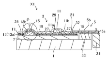
- FIG. 2 is a cross-sectional view taken along line II of the thermal head of FIG. 1.
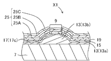
- FIG. 3 is an enlarged view of a region P shown in FIG. 2. It is a figure which shows schematic structure of one Embodiment of the thermal printer of this invention. In the area
- FIG. 8 is an enlarged view showing a modification of the thermal head shown in FIG. 7 in a region P shown in FIG. 2.
- the thermal head X ⁇ b> 1 of this embodiment includes a radiator 1, a head substrate 3 disposed on the radiator 1, and a flexible printed wiring board 5 connected to the head substrate 3 (hereinafter referred to as “head”). And FPC5).
- FIG. 1 illustration of the FPC 5 is omitted, and a region where the FPC 5 is arranged is indicated by a one-dot chain line.
- the heat radiator 1 is formed in a plate shape and has a rectangular shape in plan view.
- the radiator 1 is made of a metal material such as copper or aluminum, for example. Further, it has a function of radiating a part of heat generated in the heat generating portion 9 of the head base 3 that does not contribute to printing.
- a double-sided tape or an adhesive is provided on the upper surface of the radiator 1 so that the radiator 1 and the head base 3 are bonded to each other.
- the head substrate 3 has a rectangular substrate 7 in plan view, a plurality of heat generating portions 9 provided on the substrate 7 and arranged along the longitudinal direction of the substrate 7, and the arrangement direction of the heat generating portions 9. And a plurality of drive ICs 11 arranged side by side on the substrate 7.
- the substrate 7 is made of an electrically insulating material such as alumina ceramic or a semiconductor material such as single crystal silicon.
- a heat storage layer 13 is formed on the upper surface of the substrate 7.
- the heat storage layer 13 includes a base portion 13a formed on the entire top surface of the substrate 7, and a raised portion 13b extending in a band shape along the arrangement direction of the plurality of heat generating portions 9 and having a substantially semi-elliptical cross section. .
- the raised portion 13b functions to favorably press the recording medium to be printed onto a protective layer 25 (described later) formed on the heat generating portion 9.
- the heat storage layer 13 is made of, for example, glass having low thermal conductivity, and temporarily accumulates part of the heat generated in the heat generating part 9 to increase the temperature of the heat generating part 9. It functions to shorten the time required and improve the thermal response characteristics of the thermal head X1.
- the heat storage layer 13 is formed, for example, by applying a predetermined glass paste obtained by mixing a glass powder with an appropriate organic solvent onto the upper surface of the substrate 7 by screen printing or the like known in the art, and baking it.
- an electrical resistance layer 15 is provided on the upper surface of the heat storage layer 13.
- the electric resistance layer 15 is interposed between the heat storage layer 13 and a common electrode 17, an individual electrode 19, and an IC-FPC connection electrode 21 described later.
- FIG. 1 in a plan view, the common electrode 17, the individual electrode 19, and an area having the same shape as the IC-FPC connection electrode 21 (hereinafter referred to as an intervening area), the common electrode 17 and the individual electrode 19, In the illustrated example, there are a plurality of 24 areas (hereinafter referred to as exposure areas) exposed from between the two.
- the intervening region of the electric resistance layer 15 is hidden by the common electrode 17, the individual electrode 19, and the IC-FPC connection electrode 21.
- Each exposed region of the electrical resistance layer 15 forms the heat generating portion 9 described above.
- the some heat-emitting part 9 is arrange
- the plurality of heat generating portions 9 are illustrated in a simplified manner in FIG. 1 for convenience of explanation, but are arranged with a density of 600 dpi to 2400 dpi, for example.
- the electric resistance layer 15 is formed of a material having a relatively high electric resistance such as TaN, TaSiO, TaSiNO, TiSiO, TiSiCO, or NbSiO. Therefore, when a voltage is applied between the common electrode 17 and the individual electrode 19 described later and a current is supplied to the heat generating portion 9, the heat generating portion 9 generates heat due to Joule heat.
- a common electrode 17, a plurality of individual electrodes 19, and a plurality of IC-FPC connection electrodes 21 are provided on the upper surface of the electric resistance layer 15, more specifically on the upper surface of the intervening region.
- the common electrode 17, the individual electrode 19, and the IC-FPC connection electrode 21 are formed of a conductive material, for example, any one of aluminum, gold, silver, and copper, or an alloy thereof. Is formed by.
- the common electrode 17 is for connecting the plurality of heat generating portions 9 and the FPC 5. As shown in FIG. 1, the common electrode 17 has a main wiring portion 17a, a sub wiring portion 17b, and a lead portion 17c.
- the main wiring portion 17 a extends along one long side that is the long side on the left side of the substrate 7.
- the sub wiring part 17b extends along one and the other short sides of the substrate 7, and one end part thereof is connected to the main wiring part 17a.
- the lead portion 17c extends individually from the main wiring portion 17a toward each heat generating portion 9, and the tip portion is connected to each heat generating portion 9.
- the common electrode 17 is electrically connected between the FPC 5 and each heat generating portion 9 by connecting the other end portion on the right side of the sub-wiring portion 17b to the FPC 5.
- the plurality of individual electrodes 19 are for connecting each heat generating part 9 and the drive IC 11. As shown in FIGS. 1 and 2, each individual electrode 19 is arranged from each heat generating part 9 to the driving IC 11 so that one end is connected to the heat generating part 9 and the other end is arranged in the arrangement region of the driving IC 11. It individually extends in a strip shape toward the region. Then, the other end portion of each individual electrode 19 is connected to the drive IC 11, so that each heat generating portion 9 and the drive IC 11 are electrically connected. More specifically, the individual electrode 19 divides a plurality of heat generating portions 9 into a plurality of groups, and electrically connects the heat generating portions 9 of each group to a drive IC 11 provided corresponding to each group.
- the lead portion 17c and the individual electrode 19 of the common electrode 17 are connected to the heat generating portion 9, and the lead portion 17c and the individual electrode 19 are arranged to face each other. In this way, electrode wirings connected to the heat generating portion 9 that is an electrical resistor are formed in pairs.
- the plurality of IC-FPC connection electrodes 21 are for connecting the driving IC 11 and the FPC 5. As shown in FIGS. 1 and 2, one end of each IC-FPC connection electrode 21 is arranged in the arrangement area of the drive IC 11. Further, the other end portion extends in a band shape so as to be disposed in the vicinity of the other long side which is the long side on the right side of the substrate 7.
- the plurality of IC-FPC connection electrodes 21 have one end connected to the drive IC 11 and the other end connected to the FPC 5. Thereby, the drive IC 11 and the FPC 5 are electrically connected.
- the plurality of IC-FPC connection electrodes 21 connected to each drive IC 11 are composed of a plurality of wirings having different functions.
- the plurality of IC-FPC connection electrodes 21 are formed by, for example, an IC power supply wiring (not shown), a ground electrode wiring (not shown), and an IC control wiring.
- the IC power supply wiring has a function of supplying a power supply current for operating the driving IC 11.
- the ground electrode wiring has a function of holding the drive IC 11 and the individual electrode 19 connected to the drive IC 11 at a ground potential of 0V to 1V, for example.
- the IC control wiring has a function of supplying an electric signal for operating the driving IC 11 so as to control an on / off state of a switching element in the driving IC 11 described later.
- the drive IC 11 is disposed corresponding to each group of the plurality of heat generating units 9, and the other end of the individual electrode 19 and one end of the IC-FPC connection electrode 21. It is connected to the.
- the drive IC 11 is for controlling the energization state of each heat generating part 9, and has a plurality of switching elements inside, and is energized when each switching element is on, and each switching element is off. A well-known thing which becomes a non-energized state at the time of a state can be used.
- each drive IC 11 is provided with a plurality of switching elements inside so as to correspond to each individual electrode 19 connected to each drive IC 11.
- one connection terminal 11 a (hereinafter referred to as the first connection terminal 11 a) connected to each switching element is connected to the individual electrode 19.
- the other connection terminal 11 b (hereinafter, second connection terminal 11 b) connected to each switching element is connected to the ground electrode wiring of the IC-FPC connection electrode 21.
- the electric resistance layer 15, common electrode 17, individual electrode 19 and IC-FPC connection electrode 21 are formed by, for example, forming a material layer on each of the heat storage layers 13 by a conventionally well-known thin film forming technique such as sputtering. After sequentially laminating, the laminated body is formed by processing into a predetermined pattern using a conventionally known photoetching or the like. Note that the common electrode 17, the individual electrode 19, and the IC-FPC connection electrode 21 can be simultaneously formed by the same process.
- a protective layer 25 is formed on the heat storage layer 13 formed on the upper surface of the substrate 7 to cover the heat generating portion 9, a part of the common electrode 17 and a part of the individual electrode 19. ing.
- the formation region of the protective layer 25 is indicated by a one-dot chain line, and illustration of these is omitted.
- the protective layer 25 is provided so as to cover the left region of the upper surface of the heat storage layer 13. More specifically, a part of the heat generating part 9, a part of the common wiring 17 on the left side of the main wiring part 17 a and the sub wiring part 17 b, a part of the lead part 17 c and a part of the left side of the individual electrode 19. A protective layer 25 is formed on this region.
- the protective layer 25 protects the area covered with the heat generating portion 9, the common electrode 17 and the individual electrode 19 from corrosion due to adhesion of moisture or dust contained in the atmosphere or wear due to contact with a recording medium to be printed. Is for. As shown in FIG. 3, the protective layer 25 is formed on the upper surface of the heat generating portion 9, the first layer 25A formed on the upper surface of the common electrode 17, and the upper surface of the individual electrode 19, and the upper surface of the first layer 25A. A second layer 25B, and a third layer 25C formed on the upper surface of the second layer 25B. The protective layer 25 is directly formed on the heat generating portion 9, the common electrode 17, and the individual electrode 19.
- the first layer 25A is made of silicon carbonitride (SiCN) and is an electrical insulating layer.
- the specific resistance of SiCN is 1 ⁇ 10 9 to 1 ⁇ 10 12 ⁇ ⁇ cm.
- the thickness of the first layer 25A is, for example, 0.05 to 0.5 ⁇ m.
- the SiCN forming the first layer 25A includes those having a non-stoichiometric composition.
- the first layer 25 ⁇ / b> A is directly formed on the upper surface of the heat generating portion 9, the upper surface of the common electrode 17, and the upper surface of the individual electrode 19.
- the above-mentioned SiCN has a high thermal conductivity of 0.05 to 0.15 W / m ⁇ K, so that the heat generated by the heat generating portion 13 can be efficiently transferred. Therefore, the thermal head X1 with improved thermal response characteristics can be obtained. Thereby, the dot reproducibility of the thermal head X1 can be improved, and the thermal head X1 with less printing unevenness can be obtained.
- SiCN has a thermal expansion coefficient of 10.0 ⁇ 10 ⁇ 6 / ° C. in the temperature range where the thermal head X1 prints. Therefore, the thermal expansion coefficient of silicon oxide (SiO 2 ) that forms the second layer 25B described later can be close to 8.0 ⁇ 10 ⁇ 6 / ° C. Thereby, the adhesiveness between the first layer 25A and the second layer 25B can be improved, and the protective layer 25 which is less likely to be peeled off can be obtained. Further, since the thermal expansion coefficients of the first layer 25A and the second layer 25B are close to each other, even when the thermal head X1 becomes hot like during printing, the first layer 25A and the second layer 25B. Peeling can be suppressed.
- the first layer 25A is in contact with both the common electrode 17 and the individual electrode 19 as shown in FIG. 3, the first electrode 25A is electrically insulative as described above. 19 is prevented from being electrically short-circuited to the heat generating portion 9, the common electrode 17, and the individual electrode 19. Further, since the first layer 25A is made of SiCN and the first layer 25A itself does not contain oxygen atoms, the heat generating portion 9, the common electrode 17 and the first electrode 25 are formed by SiCN forming the first layer 25A. The structure is such that the oxidation of the individual electrode 19 is not induced.
- the first layer 25A made of SiCN is interposed between the heat generating portion 9, the common electrode 17 and the individual electrode 19 and the second layer 25B containing SiO 2 formed on the first layer 25A. ing. Therefore, the oxygen contained in SiO 2 forming the second layer 25B can be suppressed by the first layer 25A from diffusing into the heat generating part 9, the common electrode 17, and the individual electrode 19, and the heat generating part 9 The oxidation of the common electrode 17 and the individual electrode 19 can be suppressed.
- the electrical resistance of the heat generating part 9, the common electrode 17 and the individual electrode 19 can be suppressed from changing due to oxidation, and the heat generating temperature of the heat generating part 9 can be prevented from deviating from a predetermined temperature. Can do.
- the second layer 25B is made of SiO 2 and is formed on the first layer 25A.
- the thickness of the second layer 25B is 1.0 ⁇ m to 5.5 ⁇ m.
- the SiO 2 forming the second layer 25B includes those having a non-stoichiometric composition.
- the second layer 25B has a function of sealing so that the heat generating portion 9, the common electrode 17, and the individual electrode 19 are not exposed to the outside air.
- the second layer 25B is directly provided on the upper surface of the first layer 25A.
- the third layer 25C is provided on the second layer 25B and is formed of silicon carbide (SiC).
- SiC has a Vickers hardness of about 1800 Hv to 2200 Hv. Therefore, the third layer 25C can be a wear-resistant layer by forming the third layer 25C with SiC.
- the third layer 25C is directly provided on the upper surface of the second layer 25B.
- SiC has a specific resistance of 1 ⁇ 10 8 ⁇ ⁇ cm and has conductivity
- static electricity generated in the third layer 25C by forming the third layer 25C with this SiC. Can be discharged to the outside, and the possibility that the third layer 25C is destroyed by static electricity can be reduced.
- the third layer 25C is formed by non-bias sputtering as will be described later.
- the thickness of the third layer 25C is, for example, 1 ⁇ m to 6 ⁇ m.
- the SiC forming the third layer 25C can be expressed as Si 3 C 4 in the chemical formula, and includes one having a non-stoichiometric composition.
- the third layer 25C may be formed of SiC containing a large amount of carbon (hereinafter sometimes referred to as C—SiC). Even in that case, the conductivity can be further improved, and static electricity generated in the third layer 25C can be further discharged.
- the first layer 25A is formed by SiCN
- the second layer 25B is formed by SiO 2
- a third layer is formed by SiC.
- the sputtering target is SiC
- Ar + N gas is used.
- the protective layer 25 when the protective layer 25 is formed using a sputtering apparatus configured so that two sputtering targets can be accommodated in one batch and used, SiC and SiO 2 are used as sputtering targets.
- the first layer 25A, the second layer 25B, and the third layer 25C can be formed continuously, and the protective layer 25 can be formed without changing the batch. Therefore, productivity can be improved.
- the protective layer 25 can be produced
- the protective layer 25 having the first layer 25A, the second layer 25B, and the third layer 25C can be formed as follows, for example.
- the first layer 25A is formed on the heat generating portion 9, the common electrode 17, and the individual electrode 19 by a non-bias sputtering method.
- the SiCN first layer 25A is formed by non-bias sputtering using Ar gas with SiCN as a sputtering target.
- the first layer 25A may be formed by a non-bias sputtering method using an Ar + N 2 gas. Specifically, using SiC as a sputtering target, N 2 gas is mixed so that the molar ratio of N to Ar is 10 to 80 mol%, and the first layer 25A of SiCN is formed by a non-bias sputtering method. May be formed.
- the second layer 25B is formed on the first layer 25A by a non-bias sputtering method.
- the SiO 2 as a sputtering target to form a second layer 25B of SiO 2 by non-bias sputtering method using Ar gas.
- a third layer 25C is formed on the second layer 25B by a non-bias sputtering method.
- the SiC third layer 25C is formed by non-bias sputtering using Ar gas with SiC as a sputtering target.
- the C—SiCN sputtering target is facilitated and non-bias sputtering is performed using Ar gas to form the C—SiCN first layer 25A.
- Ar gas to form the C—SiCN first layer 25A.
- the first layer 25A of C—SiCN may be formed by non-bias sputtering using C—SiC as a sputtering target and an Ar + N 2 gas.
- the C—SiC first layer 25A is formed by non-bias sputtering using Ar gas with a sputtering target using C—SiC. Can be formed.
- the heat generating portion 9 may be nitrided using an Ar + N 2 gas.
- the heat generating part 9 may be made of a TaSiNO material by forming the heat generating part 9 from a TaSiO-based material and nitriding the heat generating part 9 using an Ar + N 2 gas.
- the protective layer 25 having the first layer 25A, the second layer 25B, and the third layer 25C can be formed.
- a sputtering method performed when forming each layer a well-known high frequency sputtering method etc. can be used suitably, for example.
- a coating layer 27 that partially covers the common electrode 17, the individual electrode 19, and the IC-FPC connection electrode 21 is provided on the heat storage layer 13 formed on the upper surface of the substrate 7. ing.
- the formation region of the coating layer 27 is indicated by a one-dot chain line, and illustration thereof is omitted.
- the covering layer 27 is provided so as to partially cover the region on the right side of the protective layer 25 on the upper surface of the heat storage layer 13.
- the coating layer 27 protects the area covered by the common electrode 17, the individual electrode 19, and the IC-FPC connection electrode 21 from oxidation due to contact with the atmosphere or corrosion due to adhesion of moisture contained in the atmosphere. belongs to.
- the covering layer 27 is formed so as to overlap the end portion of the protective layer 25 as shown in FIG. 2 in order to ensure the protection of the common electrode 17 and the individual electrode 19.
- the covering layer 27 can be formed of, for example, an epoxy resin or a polyimide resin material.
- the covering layer 27 can be formed using a thick film forming technique such as a screen printing method.
- the sub-wiring portion 17b of the common electrode 17 connecting the FPC 5 described later and the end of the IC-FPC connection electrode 21 are exposed from the coating layer 27, and will be described later.
- the FPC 5 is connected.
- the covering layer 27 is formed with openings 27a for exposing the individual electrodes 19 for connecting the driving IC 11 and the ends of the IC-FPC connection electrodes 21, and these wirings are connected through the openings 27a. It is connected to the driving IC 11. Further, the drive IC 11 is connected to the individual electrode 19 and the IC-FPC connection electrode 21 to protect the drive IC 11 itself and to protect the connection portion between the drive IC 11 and these wirings. It is sealed by being covered with a covering member 29 made of this resin.
- the FPC 5 extends along the longitudinal direction of the substrate 7 and is connected to the sub-wiring portion 17b of the common electrode 17 and the IC-FPC connection electrodes 21 as described above.
- the FPC 5 is a well-known one in which a plurality of printed wirings are wired inside an insulating resin layer, and each printed wiring is electrically connected to an external power supply device and control device (not shown) via a connector 31. It has become so.
- a printed wiring is generally formed of, for example, a metal foil such as a copper foil, a conductive thin film formed by a thin film forming technique, or a conductive thick film formed by a thick film printing technique.
- the printed wiring formed by a metal foil, a conductive thin film, or the like is patterned by, for example, partially etching these by photoetching or the like.
- the FPC 5 is configured such that each printed wiring 5 b formed inside the insulating resin layer 5 a is exposed at the end on the head base 3 side, and the conductive bonding material,
- the bonding material 32 (see FIG. 2) made of an anisotropic conductive material (ACF) in which conductive particles are mixed in a solder material or an electrically insulating resin is used to form the sub wiring portion 17b of the common electrode 17.
- ACF anisotropic conductive material
- the common electrode 17 When each printed wiring 5b of the FPC 5 is electrically connected to an external power supply device and a control device (not shown) via the connector 31, the common electrode 17 has a power supply held at a positive potential of 20 to 24V, for example. It is electrically connected to the positive terminal of the device.
- the individual electrode 19 is electrically connected to the negative terminal of the power supply device held at the ground potential of 0 to 1 V via the ground electrode wiring of the drive IC 11 and the IC-FPC connection electrode 21. Therefore, when the switching element of the drive IC 11 is in the on state, a current is supplied to the heat generating unit 9 and the heat generating unit 9 generates heat.
- the IC power supply wiring of the IC-FPC connection electrode 21 is Similar to the common electrode 17, it is electrically connected to the positive terminal of the power supply device held at a positive potential.
- a current for operating the drive IC 11 is supplied to the drive IC 11 by the potential difference between the IC power supply wiring and the ground electrode wiring of the IC-FPC connection electrode 21 to which the drive IC 11 is connected.
- the IC control wiring of the IC-FPC connection electrode 21 is electrically connected to an external control device that controls the driving IC 11.
- the electrical signal transmitted from the control device is supplied to the drive IC 11.
- a reinforcing plate 33 made of a resin such as a phenol resin, a polyimide resin, or a glass epoxy resin is provided between the FPC 5 and the radiator 1.
- the reinforcing plate 33 functions to reinforce the FPC 5 by being adhered to the lower surface of the FPC 5 with a double-sided tape, an adhesive, or the like.
- the FPC 5 is fixed on the radiator 1 by bonding the reinforcing plate 33 to the upper surface of the radiator 1 with a double-sided tape, an adhesive, or the like.
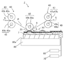
- FIG. 4 is a schematic configuration diagram of the thermal printer Z of the present embodiment.
- the thermal printer Z of the present embodiment includes the thermal head X1, the transport mechanism 40, the platen roller 50, the power supply device 60, and the control device 70 described above.
- the thermal head X1 is attached to an attachment surface 80a of an attachment member 80 provided in the casing of the thermal printer Z.
- the thermal head X1 is arranged so that the arrangement direction of the heat generating portions 9 is along the main scanning direction, which is a direction orthogonal to the conveyance direction S of the recording medium P described later, in other words, the direction orthogonal to the paper surface of FIG. , Attached to the attachment member 80.
- the transport mechanism 40 transports a recording medium P such as thermal paper or image receiving paper onto which ink is transferred in the direction of the arrow in FIG. 4, and more specifically on the plurality of heat generating units 9 of the thermal head X ⁇ b> 1. It is for carrying up, and has carrying rollers 43, 45, 47, and 49.
- the transport rollers 43, 45, 47, and 49 are formed by, for example, covering cylindrical shaft bodies 43a, 45a, 47a, and 49a made of metal such as stainless steel with elastic members 43b, 45b, 47b, and 49b made of butadiene rubber or the like. Can be configured.
- the recording medium P is an image receiving paper to which ink is transferred, an ink film is conveyed together with the recording medium P between the recording medium P and the heat generating portion 9 of the thermal head X1. Yes.
- the platen roller 50 is for pressing the recording medium P onto the heat generating portion 9 of the thermal head X1, and is arranged so as to extend along a direction orthogonal to the conveyance direction of the recording medium P, and heats the recording medium P. Both ends are supported so as to be rotatable while being pressed onto the portion 9.
- the platen roller 50 can be configured by, for example, covering a cylindrical shaft body 50a made of metal such as stainless steel with an elastic member 50b made of butadiene rubber or the like.
- the power supply device 60 is for supplying a current for causing the heat generating portion 9 of the thermal head X1 to generate heat and a current for operating the driving IC 11 as described above.
- the control device 70 is for supplying a control signal for controlling the operation of the drive IC 11 to the drive IC 11 in order to selectively generate heat in the heat generating portion 9 of the thermal head X1 as described above.
- the thermal printer Z of the present embodiment conveys the recording medium P onto the heat generating part 9 by the conveying mechanism 40 while pressing the recording medium onto the heat generating part 9 of the thermal head X1 by the platen roller 50.
- the recording medium P is an image receiving paper or the like
- printing on the recording medium P can be performed by thermally transferring the ink of the ink film conveyed together with the recording medium P to the recording medium P.
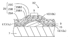
- the protective layer 25 is provided on the first layer 25A and the first layer 25A, and the second layer 25B including the adhesion layer 25B1 and the dense layer 25B2
- the third layer 25C provided on the dense layer 25B2 is the same as the thermal head X1.
- symbol is attached
- the second layer 25B is made of SiC and SiO 2 , and is formed by an adhesion layer 25B1 formed on the first layer 25A and a dense layer 25B2 formed on the adhesion layer 25B1.
- the second layer 25B is formed of SiC and SiO 2 , it is possible to improve the adhesion with SiCN forming the first layer 25A, and the first layer 25A and the second layer Bonding strength with the layer 25B can be improved.
- the third layer 25C is formed of SiC, it is possible to improve the adhesion with the SiC forming the third layer 25C, and to improve the bonding strength between the third layer 25C and the second layer 25B. Can be made.
- the adhesion layer 25B1 preferably contains 1.1 to 2.1 mol% of SiC. Accordingly, while securing the sealing property by SiO 2, it is possible to improve the thermal conductivity of the contact layer 25B1, it can be a thermal head X2 with improved thermal response.
- the dense layer 25B2 preferably contains 5.9 to 11.2 mol% of SiC. Accordingly, while securing the sealing property by SiO 2, it is possible to improve the thermal conductivity of the dense layer 25 b 2, can be the thermal head X2 with improved thermal response.
- the adhesion between the third layer 25C1 and the dense layer 25B2 can be improved. it can.
- the heat conductivity of the dense layer 25B2 that is far from the heat generating portion 9 can be made higher than the heat conductivity of the adhesion layer 25B1 that is close to the heat generating portion 9, and is in contact with a recording medium (not shown).
- the heat of the heat generating portion 9 can be accurately transferred to the surface of the protective layer 25, and the image quality can be improved.
- the thermal head X2 has a configuration in which the carbon content contained in the adhesion layer 25B1 is smaller than the carbon content contained in the first layer 25A. Therefore, the carbon content in the adhesion layer 25B1 is less than that of the first layer 25A and the dense layer 25B2.
- the adhesion layer 25B1 having a low thermal conductivity is provided between the first layer 25A and the dense layer 25B2. Therefore, the adhesion layer 25B1 has a function as a heat storage unit that temporarily stores heat from the heat generating unit 9.
- the adhesion layer 25B1 is formed by a non-bias sputtering method as will be described later.
- the thickness of the adhesion layer 25B1 is, for example, 0.5 ⁇ m to 2.5 ⁇ m.
- the dense layer 25B2 is formed by a bias sputtering method as will be described later.
- the dense layer 25B2 has a thickness of 0.5 ⁇ m to 3 ⁇ m, for example.
- the adhesive layer 25B1 is formed by the non-bias sputtering method and the dense layer 25B2 is formed by the bias sputtering method, so that the residual stress of the adhesive layer 25B1 is smaller than the residual stress of the dense layer 25B2.
- SiO 2 forming the dense layer 25B2 is denser than SiO 2 forming the adhesion layer 25B1.
- the residual stress of the adhesion layer 25A and the dense layer 25B of the second layer 25B can be measured from the bending displacement of the strip substrate. As shown in FIG. 5, the residual stress can be measured by forming a thin film on one surface of a strip-shaped substrate by sputtering, regarding the cross section of the deformed substrate as an arc, and measuring the displacement ⁇ . .
- the Young's modulus of the substrate is E
- the Poisson's ratio of the substrate is ⁇
- the length of the substrate is L
- the thickness of the substrate is b
- the thickness of the thin film is d
- the displacement of the substrate is ⁇
- the residual stress ⁇ can be obtained by a calculation formula of E ⁇ b 2 ⁇ 3 ⁇ 1 ⁇ (1 ⁇ ) ⁇ 1 ⁇ L ⁇ 2 ⁇ d ⁇ 1 ⁇ ⁇ .
- Residual stress can also be determined by X-ray diffraction or Newton ring method.
- the non-bias sputtering method in the present invention is a known bias sputtering method in which a bias voltage is applied to the film forming substrate side when sputtering is performed, whereas a bias voltage is not applied to the film forming substrate side. This refers to the sputtering method.
- the first layer 25A is formed by a non-bias sputtering method. Specifically, the first layer 25A made of SiCN is formed by non-bias sputtering using SiCN as a sputtering target.
- an adhesion layer 25B1 and a dense layer 25B2 constituting the second layer 25B are sequentially formed on the first layer 25A by a non-bias sputtering method and a bias sputtering method.
- an adhesion layer 25B1 made of SiO 2 is formed by non-bias sputtering without applying a bias voltage to the substrate 7 side using SiO 2 as a sputtering target.
- a dense layer 25B2 made of SiO 2 is formed by bias sputtering while applying a bias voltage to the substrate 7 side, similarly using SiO 2 as a sputtering target.
- the third layer 25C is formed on the dense layer 25B2 constituting the second layer 25B by a sputtering method.
- the protective layer 25 can be formed by forming the third layer 25C made of SiC by a non-bias sputtering method using SiC as a sputtering target.
- the second layer 25B containing SiO 2 and SIC is formed on the adhesion layer 25B1 formed on the first layer 25A by the non-bias sputtering method and on the adhesion layer 25B1 by the bias sputtering method. And the dense layer 25B2. Therefore, it is possible to prevent the second layer 25B from being peeled off from the first layer 25A, and it is possible to improve the sealing performance by the second layer 25B.
- the adhesion layer 25B1 is formed by the non-bias sputtering method
- the dense layer 25B2 is formed by the bias sputtering method. It is smaller than the residual stress of 25B2. Therefore, for example, when the dense layer 25B2 is formed directly on the first layer 25A by the bias sputtering method, in other words, for example, when the adhesion layer 25B1 on the first layer 25A is formed by the bias sputtering method. In comparison with the above, peeling of the second layer 25B from the first layer 25A can be suppressed.
- the adhesion layer 25B1 is formed by the non-bias sputtering method
- the dense layer 25B2 is formed by the bias sputtering method, so that SiO 2 that forms the dense layer 25B2 becomes SiO 2 that forms the adhesion layer 25B1. It is denser than 2 . Therefore, for example, when the dense layer 25B2 is not formed on the adhesion layer 25B1, in other words, for example, compared with the case where the dense layer 25B2 on the adhesion layer 25B1 is formed by the non-bias sputtering method, the second layer 25B. It is possible to improve the sealing performance. Thereby, it is possible to suppress moisture and the like contained in the atmosphere from entering the second layer 25B, and the moisture and the like adhere to the heat generating portion 9, the common electrode 17, and the individual electrode 19. Occurrence of the resulting corrosion can be suppressed.
- the SiC content of the adhesion layer 25B1 and the dense layer 25B2 can be adjusted, for example, by changing the RF voltage value applied to the SiC sputtering target.
- the SiC content of the adhesion layer 25B1 and the dense layer 25B2 may be adjusted by a generally known method.
- the thickness of the region covering the ends of the common electrode 17 and the individual electrode 19 (hereinafter referred to as a wiring end portion covering region) tends to be thin.
- the thickness of the wiring end portion covering region in the adhesion layer 25B1 and the dense layer 25B2 Tends to be thin.
- the thermal head X2 since the adhesion layer 25B1 on the first layer 25A is formed by the non-bias sputtering method, the surface of the first layer 25A may be scraped. In addition, the thickness of the wiring end portion covering region in the first layer 25A is difficult to be reduced. Further, the wiring end portion covering region in the adhesion layer 25B1 is also difficult to be thinned. Therefore, the thickness of the wiring end portion covering region in the first layer 25A and the adhesion layer 25B1 can be increased, and the sealing performance by the insulating layer 25A and the adhesion layer 25B1 can be improved. In the present embodiment, since the third layer 25C has conductivity, by securing the thickness of the first layer 25A in this manner, static electricity is generated from the third layer 25C. Also, leakage to the individual electrode 19 can be suppressed.
- the adhesion layer 25B1 is formed by the non-bias sputtering method and the dense layer 25B2 is formed by the bias sputtering method is shown, but the present invention is not limited to this. Absent. Both the adhesion layer 25B1 and the dense layer 25B2 may be formed by a non-bias sputtering method.
- the common electrode 17 and the individual electrode 19 are formed on the heat storage layer 13, and the electric resistance layer 15 is formed on the heat storage layer 13 on which the common electrode 17 and the individual electrode 19 are formed.
- the heat generating portion 9 is formed by the region of the electric resistance layer 15 located between the common electrode 17 and the individual electrode 19.
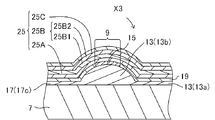
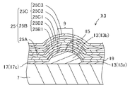
- the thermal head X3 ′ shown in FIG. 8 is a modification of the thermal head X3, and the third layer 25C is provided on the lower layer 25C1, the intermediate layer 25C2 provided on the lower layer 25C1, and the intermediate layer 25C2. And the upper layer 25C3.
- the lower layer 25C1 is made of SiON.
- the middle layer 25C2 is made of SiC.
- the upper layer 25C3 is made of SiON.
- the lower layer 25C1 has a function of improving the adhesion between the middle layer 25C2 and the dense layer 25B2.
- the adhesion between the middle layer 25C2 and the dense layer 25B2 can be improved, and the bonding strength between the middle layer 25C2 and the dense layer 25B2 can be increased.
- the middle layer 25C2 functions as an abrasion-resistant layer that reduces the wear of the protective layer 25 due to contact with the recording medium. By providing the middle layer 25C2, the protective layer 25 with improved wear resistance can be obtained.
- the upper layer 25C3 has a function of improving the slipperiness of the recording medium.
- the slipperiness of the recording medium can be improved, and the possibility of sticking to the recording medium can be reduced.
- the third layer 25C is formed of SiC, but is not limited to this.
- silicon nitride (SiN) whose chemical formula is represented by Si 3 N 4 or It may be formed of tantalum pentoxide (Ta 2 O 5 ) or the like.
- the SiN or Ta 2 O 5 forming the third layer 25C includes those having a non-stoichiometric composition.
- the third layer 25C is formed of SiN, for example, it may be formed by non-bias sputtering using SiN as a sputtering target.
- a Ta 2 O 5 may be formed by non-bias sputtering method as a sputtering target.
- the raised portion 13b is formed on the heat storage layer 13 and the electric resistance layer 15 is formed on the raised portion 13b.
- the present invention is not limited to this.
- the heat generating portion 9 of the electric resistance layer 15 may be disposed on the base portion 13 b of the heat storage layer 13 without forming the raised portion 13 b in the heat storage layer 13.
- the electric resistance layer 15 may be disposed on the substrate 7 without forming the heat storage layer 13.
- the present invention is not limited thereto, and for example, the heat generating portion 9 may be provided on the side surface of the substrate 7. Specifically, the heat generating portion 9 may be provided on a side surface connecting one main surface of the substrate 7 and the other main surface. Even in that case, a thermal head with improved thermal response can be obtained.
- the example of the external wiring board connected to the head base 3 is FPC, it is not limited to this.
- a rigid substrate obtained by curing an organic resin may be used.
- the third layer 25C is provided on the second layer 25B.
- the present invention is not limited to this. Even when the protective layer 25 includes only the first layer 25A and the second layer 25B, the first layer 25A contains SiCN, so that the thermal head X1 with improved thermal response characteristics is obtained. Can do.
Landscapes
- Electronic Switches (AREA)
Abstract
Description
以下、本発明のサーマルヘッドの一実施形態について、図面を参照しつつ説明する。図1,2に示すように、本実施形態のサーマルヘッドX1は、放熱体1と、放熱体1上に配置されたヘッド基体3と、ヘッド基体3に接続されたフレキシブルプリント配線板5(以下、FPC5という)とを備えている。なお、図1では、FPC5の図示を省略し、FPC5が配置される領域を一点鎖線で示す。
以下、第2の実施形態に係るサーマルヘッドX2について図5を用いて説明する。
図7,8を用いて第3の実施形態に係るサーマルヘッドX3について説明する。
Z サーマルプリンタ
1 放熱体
3 ヘッド基体
5 フレキシブルプリント配線板
7 基板
9 発熱部
11 駆動IC
17 共通電極
17a 主配線部
17b 副配線部
17c リード部
19 個別電極
21 IC-FPC接続電極
25 保護層
25A 第1の層
25B 第2の層
25B1 密着層
25B2 緻密層
25C 第3の層
25C1 下層
25C2 中層
25C3 上層
27 被覆層
Claims (7)
- 基板と、
該基板上に設けられた電極と、
該電極に接続された発熱部と、
該発熱部に設けられた保護層と、を備え、
該保護層は、前記発熱部に設けられた炭窒化珪素を含む第1の層と、該第1の層に設けられた酸化珪素を含む第2の層とを有することを特徴とするサーマルヘッド。 - 前記保護層は、前記第2の層に設けられた炭化珪素、窒化珪素、炭窒化珪素、または五酸化タンタルを含む第3の層をさらに有することを特徴とする請求項1に記載のサーマルヘッド。
- 前記第2の層が炭化珪素をさらに含んでなることを特徴とする請求項1または2に記載のサーマルヘッド。
- 前記第2の層が、前記第1の層に設けられた密着層と、該密着層に設けられた緻密層とを含み、
該緻密層に含有された炭化珪素の含有率が、前記密着層に含有された炭化珪素の含有率よりも多いことを特徴とする請求項3に記載のサーマルヘッド。 - 前記密着層に含有された炭素の含有率が、前記第1の層に含有された炭素の含有率よりも少ないことを特徴とする請求項4に記載のサーマルヘッド。
- 前記密着層の残留応力が、前記緻密層の残留応力よりも小さいことを特徴とする請求項4または5に記載のサーマルヘッド。
- 請求項1乃至6のいずれかに記載のサーマルヘッドと、前記保護層上に記録媒体を搬送する搬送機構と、前記保護層上に前記記録媒体を押圧するプラテンローラとを備えることを特徴とするサーマルプリンタ。
Priority Applications (3)
| Application Number | Priority Date | Filing Date | Title |
|---|---|---|---|
| US14/117,917 US8885005B2 (en) | 2011-05-16 | 2012-05-15 | Thermal head and thermal printer provided with same |
| JP2013515164A JP5669935B2 (ja) | 2011-05-16 | 2012-05-15 | サーマルヘッドおよびこれを備えるサーマルプリンタ |
| CN201280018782.0A CN103492186B (zh) | 2011-05-16 | 2012-05-15 | 热敏头以及具备该热敏头的热敏打印机 |
Applications Claiming Priority (2)
| Application Number | Priority Date | Filing Date | Title |
|---|---|---|---|
| JP2011109945 | 2011-05-16 | ||
| JP2011-109945 | 2011-05-16 |
Publications (1)
| Publication Number | Publication Date |
|---|---|
| WO2012157641A1 true WO2012157641A1 (ja) | 2012-11-22 |
Family
ID=47176958
Family Applications (1)
| Application Number | Title | Priority Date | Filing Date |
|---|---|---|---|
| PCT/JP2012/062407 Ceased WO2012157641A1 (ja) | 2011-05-16 | 2012-05-15 | サーマルヘッドおよびこれを備えるサーマルプリンタ |
Country Status (4)
| Country | Link |
|---|---|
| US (1) | US8885005B2 (ja) |
| JP (1) | JP5669935B2 (ja) |
| CN (1) | CN103492186B (ja) |
| WO (1) | WO2012157641A1 (ja) |
Families Citing this family (3)
| Publication number | Priority date | Publication date | Assignee | Title |
|---|---|---|---|---|
| JP6367962B2 (ja) * | 2014-10-30 | 2018-08-01 | 京セラ株式会社 | サーマルヘッド、およびサーマルプリンタ |
| CN108056831B (zh) * | 2017-12-27 | 2021-09-10 | 海盐纵诚物资有限公司 | 超声洁牙装置 |
| WO2021206169A1 (ja) * | 2020-04-10 | 2021-10-14 | ローム株式会社 | サーマルプリントヘッド及びその製造方法並びにサーマルプリンタ |
Citations (5)
| Publication number | Priority date | Publication date | Assignee | Title |
|---|---|---|---|---|
| JP2003094707A (ja) * | 2001-09-27 | 2003-04-03 | Kyocera Corp | サーマルヘッド |
| JP2003103820A (ja) * | 2001-09-27 | 2003-04-09 | Kyocera Corp | サーマルヘッド |
| JP2010149515A (ja) * | 2008-11-26 | 2010-07-08 | Kyocera Corp | 記録ヘッドおよびこれを備える記録装置 |
| JP2010194856A (ja) * | 2009-02-25 | 2010-09-09 | Kyocera Corp | 記録ヘッドおよびこれを備えている記録装置 |
| JP2011005715A (ja) * | 2009-06-25 | 2011-01-13 | Kyocera Corp | ヘッド基体および記録ヘッドならびに記録装置 |
Family Cites Families (13)
| Publication number | Priority date | Publication date | Assignee | Title |
|---|---|---|---|---|
| CN1086639C (zh) * | 1994-05-31 | 2002-06-26 | 罗姆股份有限公司 | 感热式打印头、打印头中所用基板及该基板的制造方法 |
| CN1086640C (zh) * | 1994-06-21 | 2002-06-26 | 罗姆股份有限公司 | 热打印头和用于打印头的基片以及该基片的制造方法 |
| JP3069247B2 (ja) * | 1994-07-29 | 2000-07-24 | アルプス電気株式会社 | サーマルヘッド |
| WO2000076775A1 (en) * | 1999-06-15 | 2000-12-21 | Rohm Co., Ltd. | Thermal print head and method of manufacture thereof |
| CN1244453C (zh) * | 2003-02-20 | 2006-03-08 | 祥群科技股份有限公司 | 热转印元件的结构及制造方法 |
| JP4619102B2 (ja) * | 2004-10-27 | 2011-01-26 | 京セラ株式会社 | サーマルヘッド及びサーマルプリンタ |
| CN100430232C (zh) * | 2004-10-27 | 2008-11-05 | 京瓷株式会社 | 热敏头与热敏头的制造方法以及热敏打印机 |
| JP2008000947A (ja) * | 2006-06-21 | 2008-01-10 | Rohm Co Ltd | サーマルプリントヘッド |
| JP2008207439A (ja) * | 2007-02-26 | 2008-09-11 | Rohm Co Ltd | サーマルプリントヘッド |
| US7837886B2 (en) * | 2007-07-26 | 2010-11-23 | Hewlett-Packard Development Company, L.P. | Heating element |
| US8319809B2 (en) * | 2008-01-31 | 2012-11-27 | Kyocera Corporation | Recording head and recording device |
| CN102076502B (zh) * | 2008-06-26 | 2014-04-23 | 京瓷株式会社 | 记录头以及具有该记录头的记录装置 |
| US8493423B2 (en) * | 2009-01-28 | 2013-07-23 | Kyocera Corporation | Thermal recording head and thermal recording apparatus comprising the same |
-
2012
- 2012-05-15 WO PCT/JP2012/062407 patent/WO2012157641A1/ja not_active Ceased
- 2012-05-15 CN CN201280018782.0A patent/CN103492186B/zh active Active
- 2012-05-15 JP JP2013515164A patent/JP5669935B2/ja active Active
- 2012-05-15 US US14/117,917 patent/US8885005B2/en not_active Expired - Fee Related
Patent Citations (5)
| Publication number | Priority date | Publication date | Assignee | Title |
|---|---|---|---|---|
| JP2003094707A (ja) * | 2001-09-27 | 2003-04-03 | Kyocera Corp | サーマルヘッド |
| JP2003103820A (ja) * | 2001-09-27 | 2003-04-09 | Kyocera Corp | サーマルヘッド |
| JP2010149515A (ja) * | 2008-11-26 | 2010-07-08 | Kyocera Corp | 記録ヘッドおよびこれを備える記録装置 |
| JP2010194856A (ja) * | 2009-02-25 | 2010-09-09 | Kyocera Corp | 記録ヘッドおよびこれを備えている記録装置 |
| JP2011005715A (ja) * | 2009-06-25 | 2011-01-13 | Kyocera Corp | ヘッド基体および記録ヘッドならびに記録装置 |
Also Published As
| Publication number | Publication date |
|---|---|
| JP5669935B2 (ja) | 2015-02-18 |
| US20140232807A1 (en) | 2014-08-21 |
| JPWO2012157641A1 (ja) | 2014-07-31 |
| US8885005B2 (en) | 2014-11-11 |
| CN103492186B (zh) | 2016-04-20 |
| CN103492186A (zh) | 2014-01-01 |
Similar Documents
| Publication | Publication Date | Title |
|---|---|---|
| JP5864608B2 (ja) | サーマルヘッドおよびこれを備えるサーマルプリンタ | |
| JP6181244B2 (ja) | サーマルヘッドおよびこれを備えるサーマルプリンタ | |
| JP5918383B2 (ja) | サーマルヘッドおよびこれを備えるサーマルプリンタ | |
| JP5669935B2 (ja) | サーマルヘッドおよびこれを備えるサーマルプリンタ | |
| JP2012030439A (ja) | サーマルヘッドおよびこれを備えるサーマルプリンタ | |
| WO2017073681A1 (ja) | サーマルヘッドおよびサーマルプリンタ | |
| JP6258783B2 (ja) | サーマルヘッドおよびこれを備えるサーマルプリンタ | |
| JP5944636B2 (ja) | サーマルヘッドおよびこれを備えるサーマルプリンタ | |
| JP6584641B2 (ja) | サーマルヘッドおよびサーマルプリンタ | |
| JP6356539B2 (ja) | サーマルヘッドおよびサーマルプリンタ | |
| JP5744171B2 (ja) | サーマルヘッドおよびこれを備えるサーマルプリンタ | |
| JP6189715B2 (ja) | サーマルヘッドおよびサーマルプリンタ | |
| JP6039795B2 (ja) | サーマルヘッドおよびサーマルプリンタ | |
| JP5780715B2 (ja) | サーマルヘッドおよびこれを備えるサーマルプリンタ | |
| JP6208607B2 (ja) | サーマルヘッド、サーマルヘッドの製造方法、およびサーマルプリンタ | |
| JP2014144623A (ja) | サーマルヘッドおよびサーマルプリンタ | |
| JP6426541B2 (ja) | サーマルヘッドおよびサーマルプリンタ | |
| JP2017043013A (ja) | サーマルヘッドおよびサーマルプリンタ | |
| JP6401078B2 (ja) | サーマルヘッドおよびこれを備えるサーマルプリンタ | |
| JPWO2020067424A1 (ja) | サーマルヘッドおよびサーマルプリンタ | |
| JP2015027758A (ja) | サーマルヘッドおよびこれを備えるサーマルプリンタ |
Legal Events
| Date | Code | Title | Description |
|---|---|---|---|
| WWE | Wipo information: entry into national phase |
Ref document number: 201280018782.0 Country of ref document: CN |
|
| 121 | Ep: the epo has been informed by wipo that ep was designated in this application |
Ref document number: 12785240 Country of ref document: EP Kind code of ref document: A1 |
|
| ENP | Entry into the national phase |
Ref document number: 2013515164 Country of ref document: JP Kind code of ref document: A |
|
| WWE | Wipo information: entry into national phase |
Ref document number: 14117917 Country of ref document: US |
|
| NENP | Non-entry into the national phase |
Ref country code: DE |
|
| 122 | Ep: pct application non-entry in european phase |
Ref document number: 12785240 Country of ref document: EP Kind code of ref document: A1 |