WO2012157507A1 - 表面処理剤及び表面処理方法 - Google Patents
表面処理剤及び表面処理方法 Download PDFInfo
- Publication number
- WO2012157507A1 WO2012157507A1 PCT/JP2012/061972 JP2012061972W WO2012157507A1 WO 2012157507 A1 WO2012157507 A1 WO 2012157507A1 JP 2012061972 W JP2012061972 W JP 2012061972W WO 2012157507 A1 WO2012157507 A1 WO 2012157507A1
- Authority
- WO
- WIPO (PCT)
- Prior art keywords
- group
- surface treatment
- compound
- acid
- substrate
- Prior art date
- Legal status (The legal status is an assumption and is not a legal conclusion. Google has not performed a legal analysis and makes no representation as to the accuracy of the status listed.)
- Ceased
Links
Classifications
-
- H—ELECTRICITY
- H10—SEMICONDUCTOR DEVICES; ELECTRIC SOLID-STATE DEVICES NOT OTHERWISE PROVIDED FOR
- H10P—GENERIC PROCESSES OR APPARATUS FOR THE MANUFACTURE OR TREATMENT OF DEVICES COVERED BY CLASS H10
- H10P50/00—Etching of wafers, substrates or parts of devices
-
- C—CHEMISTRY; METALLURGY
- C08—ORGANIC MACROMOLECULAR COMPOUNDS; THEIR PREPARATION OR CHEMICAL WORKING-UP; COMPOSITIONS BASED THEREON
- C08G—MACROMOLECULAR COMPOUNDS OBTAINED OTHERWISE THAN BY REACTIONS ONLY INVOLVING UNSATURATED CARBON-TO-CARBON BONDS
- C08G77/00—Macromolecular compounds obtained by reactions forming a linkage containing silicon with or without sulfur, nitrogen, oxygen or carbon in the main chain of the macromolecule
- C08G77/04—Polysiloxanes
- C08G77/12—Polysiloxanes containing silicon bound to hydrogen
-
- C—CHEMISTRY; METALLURGY
- C08—ORGANIC MACROMOLECULAR COMPOUNDS; THEIR PREPARATION OR CHEMICAL WORKING-UP; COMPOSITIONS BASED THEREON
- C08G—MACROMOLECULAR COMPOUNDS OBTAINED OTHERWISE THAN BY REACTIONS ONLY INVOLVING UNSATURATED CARBON-TO-CARBON BONDS
- C08G77/00—Macromolecular compounds obtained by reactions forming a linkage containing silicon with or without sulfur, nitrogen, oxygen or carbon in the main chain of the macromolecule
- C08G77/04—Polysiloxanes
- C08G77/22—Polysiloxanes containing silicon bound to organic groups containing atoms other than carbon, hydrogen and oxygen
- C08G77/26—Polysiloxanes containing silicon bound to organic groups containing atoms other than carbon, hydrogen and oxygen nitrogen-containing groups
-
- C—CHEMISTRY; METALLURGY
- C09—DYES; PAINTS; POLISHES; NATURAL RESINS; ADHESIVES; COMPOSITIONS NOT OTHERWISE PROVIDED FOR; APPLICATIONS OF MATERIALS NOT OTHERWISE PROVIDED FOR
- C09K—MATERIALS FOR MISCELLANEOUS APPLICATIONS, NOT PROVIDED FOR ELSEWHERE
- C09K3/00—Materials not provided for elsewhere
- C09K3/18—Materials not provided for elsewhere for application to surfaces to minimize adherence of ice, mist or water thereto; Thawing or antifreeze materials for application to surfaces
Definitions
- the present invention relates to a surface treatment agent and a surface treatment method for improving the water repellency of a surface of an object to be treated, and more specifically, a surface treatment agent for making a substrate surface of a liquid crystal, a semiconductor or the like to which a lithography technique is applied to be water repellent.
- the present invention also relates to a surface treatment method for making a substrate surface water repellent using the surface treatment agent.
- lithography technology is used when processing such as etching on a substrate.
- a photosensitive resin layer is provided on a substrate using a photosensitive resin composition, and then exposed to selective irradiation with actinic radiation for exposure and development, and then a photosensitive resin layer. Is selectively dissolved and removed, a resin pattern is formed on the substrate, and an etching process is performed using the resin pattern as a mask, whereby a pattern to be etched is formed on the substrate.
- a photosensitive resin layer is formed in order to build a plurality of types of elements and circuits on the substrate.
- the surface of a semiconductor substrate to which lithography technology is applied can be a mixture of various surface states, such as a previously formed surface or a surface after being removed by etching.
- a SiO 2 film is usually formed on the surface of a silicon wafer before manufacturing a semiconductor product, and moisture in the atmosphere is bonded to the outermost surface of the SiO 2 film to form Si—OH.
- Patent Document 1 discloses a method for trimethylsilylation by reacting hexamethyldisilazane with an OH group on an oxidized silicon wafer surface after oxidizing the silicon wafer surface. Is disclosed. It is also known that such a water repellency treatment can improve the adhesion between the substrate surface and the resist resin.
- Patent Document 2 as a method for preventing pattern collapse, a method for treating a substrate surface using a surface treatment solution obtained by diluting a silylating agent such as N, N-dimethylaminotrimethylsilane or hexamethyldisilazane with an organic solvent. Is disclosed.
- Patent Document 3 a plurality of convex patterns having a hydroxyl group on the surface formed on a semiconductor substrate, a surface treatment agent containing a silane coupling agent having a hydrolyzable group that reacts with the hydroxyl group, It is disclosed that a water-repellent protective film having low wettability to water can be formed, and that the water repellency is increased by cleaning the substrate surface using sulfuric acid and hydrogen peroxide.
- Patent Documents 2 and 3 as a method for evaluating the water repellency of the substrate surface, it is described that a contact angle to water is measured, and those having a large contact angle value can suppress pattern collapse. It is known that increasing the contact angle is a solution to pattern collapse.
- Patent Document 3 describes that surface treatment with a surface treatment agent can be used for a silicon nitride film, but in the case of a silicon-based film, contact with water after forming a water-repellent protective film. In contrast to the angle of 89 degrees, in the case of a silicon nitride film, only about 46 degrees can be obtained, and the contact angle is improved to 59 degrees by converting the silicon nitride film surface to SiO 2 with an oxidizing agent. There is a description.
- the silicon nitride film is easier to obtain a dense film quality than the oxide film, and also has a characteristic as an antireflection film. Therefore, the silicon nitride film is a material frequently used in recent highly integrated semiconductor devices. A method for providing sufficient water repellency to the surface of the material has been demanded.
- the subject of this invention is providing the surface treating agent which improves the water repellency of the surface of to-be-processed objects, such as a board
- Another object of the present invention is to provide a method for making the surface of an object to be treated such as a semiconductor substrate water repellent using the surface treating agent.
- the present invention is shown below. 1.
- the surface treating agent characterized by including the compound (A) represented by following General formula (1).
- R 6 is a hydrogen atom or an alkyl group having 1 to 6 carbon atoms
- R 1 , R 2 , R 3 , R 4 and R 5 are each independently a hydrogen atom, a cyanoalkyl group,
- a, w, x, y and z are each independently 0 or a positive number, at least one of w and x is a positive number, 0 ⁇ w / (x + y) ⁇ 5, 0 ⁇ z / (a + w + x + y) ⁇ 1.
- Compound A may contain only 1 type of each structural unit, and may contain 2 or more types. ] 2.
- R 3 and R 5 are each independently a hydrogen atom, an alkyl group, an aralkyl group, a cycloalkyl group, a cycloaralkyl group or an aryl group, and w, x and y are independently of each other, It is a positive number and z is 0 or a positive number.
- 3. The surface treating agent according to 1 above, wherein at least one of R 1 , R 2 , R 3 , R 4 and R 5 in the general formula (1) is a cyanoalkyl group. 4). 4. The surface treating agent according to 3 above, wherein the compound (A) is represented by the following general formula (7).
- B is a cyanoalkyl group
- b, x, y and z are each independently 0 or a positive number
- c is a positive number.
- R 11 , R 12 and R 13 are each independently a hydrogen atom, alkyl group, aralkyl group, cycloalkyl group, cycloaralkyl group or aryl group
- R 14 and R 15 are independently A hydrogen atom, a saturated or unsaturated alkyl group, a saturated or unsaturated cycloalkyl group, a trimethylsilyl group, a dimethylsilyl group, or a saturated or unsaturated heterocycloalkyl group, and R 14 and R 15 are bonded to each other. Or a saturated or unsaturated heterocycloalkyl group having a nitrogen atom. ] 8).
- the surface treatment method according to 11 or 12 above, wherein the object to be treated contains silicon nitride on a part of its surface. 14 14. The surface treatment method according to any one of 11 to 13, wherein the object to be treated includes silicon oxide on a part of the surface thereof. 15. The surface treatment method according to any one of the above 11 to 14, wherein the object to be treated contains metallic silicon in a part of its surface. 16. The surface treatment method according to any one of 11 to 15, further comprising an acid contact step in which an acidic liquid containing an acid is brought into contact with the object to be processed before the contact step. 17. 17. The surface treatment method according to 16 above, wherein the acid is an inorganic acid having an acid dissociation constant (pKa) of less than 0. 18.
- pKa acid dissociation constant
- the object to be processed has a silicon nitride film and a silicon oxide film on the surface thereof, and after the contact step, the contact angle (Can) of water on the surface of the silicon nitride film and the surface of the silicon oxide film 18.
- a surface treatment method for making a surface of a semiconductor substrate water repellent a first step of bringing an acid liquid containing an acid into contact with the semiconductor substrate, and a surface treatment agent containing a compound represented by the following general formula (11):
- a surface treatment method comprising sequentially providing a second step of contacting the semiconductor substrate.
- R 11 , R 12 and R 13 are each independently a hydrogen atom, alkyl group, aralkyl group, cycloalkyl group, cycloaralkyl group or aryl group
- R 14 and R 15 are independently A hydrogen atom, a saturated or unsaturated alkyl group, a saturated or unsaturated cycloalkyl group, a trimethylsilyl group, a dimethylsilyl group, or a saturated or unsaturated heterocycloalkyl group, and R 14 and R 15 are bonded to each other. Or a saturated or unsaturated heterocycloalkyl group having a nitrogen atom.
- the semiconductor substrate has a silicon nitride film and a silicon oxide film on its surface, and after the second step, the contact angle (Can) of water on the surface of the silicon nitride film and the surface of the silicon oxide film 24.
- the surface treating agent of the present invention it is possible to improve the water repellency by forming a film on the surface of an object to be treated such as a substrate used for a liquid crystal or a semiconductor. It is known that the surface of a water-repellent semiconductor substrate or the like has good adhesion to a resist resin, and it is known that the problem of so-called pattern collapse does not occur.
- the surface treatment agent of the present invention improves the yield of semiconductor manufacturing. Can be expected to do.
- the surface of the substrate having different surface materials and states can be made water repellent to the same extent, so that the yield is particularly high in a semiconductor substrate or the like in which patterns made of different materials are mixed. The improvement effect can be expected.
- the contact angle is a value measured using water by a method according to JIS R1257.
- the surface treating agent of the present invention contains a compound (A) represented by the following general formula (1), and if necessary, contains other silicone compounds, organic solvents, additives and the like.
- R 6 is a hydrogen atom or an alkyl group having 1 to 6 carbon atoms
- R 1 , R 2 , R 3 , R 4 and R 5 are each independently a hydrogen atom, a cyanoalkyl group,
- a, w, x, y and z are each independently 0 or a positive number, at least one of w and x is a positive number, 0 ⁇ w / (x + y) ⁇ 5, 0 ⁇ z / (a + w + x + y) ⁇ 1.
- Compound A may contain only 1 type of each structural unit, and may contain 2 or more types.
- the said compound (A) is a silicon compound containing the structural unit shown below as represented by the said General formula (1).
- the content rate of each structural unit is based on prescription
- the said compound (A) may not contain all the structural units.
- the compound (A) represented by the general formula (1) is a kind of polysiloxane in which structural units represented by (SiO 4/2 ) and the like are bonded to each other through a siloxane bond,
- the bonding form of the structural units may not necessarily be the arrangement order of the general formula (1).
- a, w, x, y, z represent the composition ratio (molar ratio) of each structural unit.
- the compound (A) since any one of R 1 , R 2 , R 3 , R 4 and R 5 is a hydrogen atom, the compound (A) has an Si—H bond having chemical reactivity. Will be included. Si—H bonds are sometimes referred to as Si—H groups or hydrosilyl groups.
- the number average molecular weight (Mn) of the compound (A) represented by the general formula (1) is preferably 120 or more and 20000 or less, more preferably 200 or more and 10,000 or less, and further preferably 240 or more and 10,000 or less.
- Mn number average molecular weight
- a surface treating agent containing the compound (A) having Mn in the above range is used, a highly water-repellent film can be formed, and in particular, a water-repellent film can be efficiently formed even on fine uneven surfaces. .
- a preferred compound (A) is a compound represented by the following general formulas (2) to (6) from the viewpoint of water repellency, and more preferred compounds are represented by the general formulas (3) and (4), and particularly preferred compounds.
- the compound represented by the general formula (3) has a trifunctional structural unit having both a Si—O bond and a Si—H bond, and the compound represented by the general formula (4) includes two Si— It has a structural unit having both an O bond and a Si—H bond.
- R 2 , R 4 and R 5 are each independently a hydrogen atom, an alkyl group, an aralkyl group, a cycloalkyl group or an aryl group, and R 6 is a hydrogen atom or a carbon atom number of 1 to 6
- x and y are positive numbers
- z is 0 or a positive number
- the ratio of x / y is preferably 0.5 to 2000, more preferably 1 to 200.
- R 5 independently of one another represents a hydrogen atom, an alkyl group, an aralkyl group, a cycloalkyl group or an aryl group
- R 6 represents a hydrogen atom or an alkyl group having 1 to 6 carbon atoms
- w and y are positive numbers
- z is 0 or a positive number
- the ratio of w / y is preferably 0.3 to 5.0.
- R 3 and R 5 are each independently a hydrogen atom, an alkyl group, an aralkyl group, a cycloalkyl group or an aryl group
- R 6 is a hydrogen atom or an alkyl group having 1 to 6 carbon atoms.
- w, x and y are positive numbers
- z is 0 or a positive number.
- R 2 and R 3 each independently represent a hydrogen atom, an alkyl group, an aralkyl group, a cycloalkyl group, a cycloaralkyl group or an aryl group.
- x is preferably 0.1 to 0.9, more preferably 0.2 to 0.5 and w are preferably 0.05 to 0.5, more preferably 0.1 to 0.4, and y is preferably 0.05 to 0.5, more preferably 0.1 to 0.00. 4, z is preferably 0.001 to 0.2, more preferably 0.005 to 0.1.
- the compound (A) in which at least one of R 1 , R 2 , R 3 , R 4 and R 5 in the general formula (1) is a cyanoalkyl group is also a preferred embodiment, and particularly preferably at least R A compound in which 1 is a cyanoalkyl group.
- a compound in which two or more of R 1 , R 2 , R 3 , R 4 and R 5 are cyanoalkyl groups may be used, and preferred examples in that case include, for example, R 1 and R 5 .
- the cyanoalkyl group is represented by NC—R 7 —.
- R 7 is a linear or branched divalent alkyl group having 1 to 5 carbon atoms.
- R 7 preferably has 1 to 3 carbon atoms.
- Specific examples of the cyanoalkyl group include a cyanomethyl group, a cyanoethyl group, a cyanopropyl group, and the like. In the present invention, a cyanoethyl group or a cyanopropyl group is more preferable, and a cyanoethyl group is particularly preferable.
- the ratio of x / y is preferably 0.1 to 200, more preferably 0.5 to 20.
- the ratio of w / y when w and y are not 0 is preferably 0.3 to 5.0.
- a preferred compound is represented by the following general formula (7).
- B is cyanoalkyl group, R 2, R 3, R 4 and R 5, independently of one another, a hydrogen atom, an alkyl group, an aralkyl group, a cycloalkyl group or an aryl group
- R 6 Is a hydrogen atom or an alkyl group having 1 to 6 carbon atoms
- b, x, y and z are each independently 0 or a positive number
- c is a positive number.
- a more preferable compound can be represented by the following general formula (8).
- B is a cyanoalkyl group
- R 3 and R 5 are each independently an alkyl group, an aralkyl group, a cycloalkyl group or an aryl group
- R 6 is a hydrogen atom or a carbon atom of 1 -6 alkyl groups
- b, x, y and z are independently of each other 0 or a positive number
- c is a positive number.
- the compound represented by the general formula (8) is also a kind of polysiloxane.
- R 2 , R 4 and R 5 are each independently a hydrogen atom, a cyanoalkyl group, an alkyl group, an aralkyl group, a cycloalkyl group or an aryl group, and R 2 , R 4 and R 5 are At least one of them is a cyanoalkyl group, R 6 is a hydrogen atom or an alkyl group having 1 to 6 carbon atoms, x and y are positive numbers, and z is 0 or a positive number.
- X / y ratio is preferably 0.1 to 200, more preferably 0.5 to 20.
- one R 5 is a cyanoalkyl group
- the other R 5 is independently a hydrogen atom, an alkyl group, an aralkyl group, a cycloalkyl group or an aryl group
- R 6 is a hydrogen atom.
- An atom or an alkyl group having 1 to 6 carbon atoms, w and y are positive numbers, z is 0 or a positive number, and the ratio of w / y is preferably 0.3 to 5.0. More preferably, it is 0.8 to 4.0.
- the manufacturing method of the said compound (A) is not specifically limited, The method of using for the raw material organosilicon compound which forms each structural unit to hydrolytic condensation on acidic conditions is common.
- the structural unit (i) tetramethoxysilane, tetraethoxysilane, tetrapropoxysilane, tetrachlorosilane, or the like can be used as a raw material organic silicon compound.
- trimethoxysilane, triethoxysilane, tripropoxysilane, trichlorosilane, cyanopropyltrimethoxysilane, cyanoethyltriethoxysilane, or the like can be used as the raw material organic silicon compound.
- dimethoxymethylsilane, diethoxymethylsilane, dipropoxymethylsilane, dichloromethylsilane, or the like can be used as a raw material organic silicon compound.
- methoxytrimethylsilane, chlorotrimethylsilane, trimethylsilanol, hexamethyldisiloxane, tetramethyldisiloxane, or the like can be used as a raw material organic silicon compound.
- methanol, ethanol, propanol, s-butanol, or the like can be used.
- the surface treating agent of the present invention may contain only one kind of the above compound (A), or may contain two or more kinds. For example, you may combine the compound represented by the said General formula (4), and the compound represented by the said General formula (7).
- the surface treating agent of the present invention contains the compound (A) represented by the general formula (1) and may be composed only of the compound (A), or the compound (A) and other repellent materials. It may consist of a hydrating agent. As another water repellent, a compound represented by the following general formula (11) (hereinafter referred to as “compound (B)”) is preferable.
- R 11 , R 12 and R 13 are each independently a hydrogen atom, alkyl group, aralkyl group, cycloalkyl group, cycloaralkyl group or aryl group
- R 14 and R 15 are independently A hydrogen atom, a saturated or unsaturated alkyl group, a saturated or unsaturated cycloalkyl group, a trimethylsilyl group, a dimethylsilyl group, or a saturated or unsaturated heterocycloalkyl group, and R 14 and R 15 are bonded to each other. Or a saturated or unsaturated heterocycloalkyl group having a nitrogen atom.
- Examples of the compound (B) include N, N-dimethylaminotrimethylsilane (hereinafter abbreviated as “DMATMS”), N, N-dimethylaminotriethylsilane, N, N-diphenylaminotriethylsilane, N, N-diethylaminotrimethyl.
- DMATMS N, N-dimethylaminotrimethylsilane
- N, N-dimethylaminotriethylsilane N, N-diphenylaminotriethylsilane
- N-diethylaminotrimethyl N, N-diethylaminotrimethyl.
- the content ratio of the compound (A) and the compound (B) is not limited.
- the sum total of a compound (A) and a compound (B) is 100 mass%, the ratio of a compound (B) becomes like this.
- it is less than 60 mass%, More preferably, it is 1 to 40 mass%.
- the surface treatment agent of the present invention may further contain an organic solvent and additives (pH adjuster, leveling agent, surfactant, silane coupling agent, stabilizer, etc.).
- an organic solvent a solvent that dissolves the compound (A) or a solvent that does not dissolve the compound (A) but disperses the compound (A) and additives can be used.
- a compound capable of dissolving the compound (A) is preferable because a surface treatment agent having a more uniform concentration distribution can be obtained.
- substrate of a semiconductor or the to-be-etched pattern surface can be used.
- sulfoxides such as dimethylsulfoxide; sulfones such as dimethylsulfone, diethylsulfone, bis (2-hydroxyethyl) sulfone, tetramethylenesulfone; N, N-dimethylformamide, N-methylformamide, N, N Amides such as dimethylacetamide, N-methylacetamide, N, N-diethylacetamide; N-methyl-2-pyrrolidone, N-ethyl-2-pyrrolidone, N-propyl-2-pyrrolidone, N-hydroxymethyl-2 -Lactams such as pyrrolidone and N-hydroxyethyl-2-pyrrolidone; 1,3-dimethyl-2-imidazolidinone, 1,3-diethyl-2-imidazolidinone, 1,3-diisopropyl-2-imidazolidi
- Non-imidazolidinones such as non-dimethyl ether, die
- organic solvents those having a relatively small polarity and a small molecular weight are preferred. However, if the molecular weight is too small, the volatility is too high and handling becomes difficult. Accordingly, preferred organic solvents are linear or branched hydrocarbon solvents or terpene solvents having 6 to 12 carbon atoms, and specifically include n-hexane, n-heptane, n-octane. N-nonane, methyloctane, n-decane, n-undecane, n-dodecane and the like.
- Terpene solvents include p-menthane, o-menthane, m-menthan and other menthane, diphenylmenthane, limonene, ⁇ -terpinene, ⁇ -terpinene, ⁇ -terpinene and other terpinenes, bornane, norbornane, pinane, ⁇ -Pinenes such as pinene and ⁇ -pinene, monoterpenes such as karan and longifolene, diterpenes such as abiethane, and the like.
- These organic solvents may be used alone or in combination of two or more. More preferred organic solvents are linear hydrocarbon solvents having 7 to 10 carbon atoms, menthane and pinane, particularly preferably hexane and octane.
- the concentration of the compound (A) or the concentration of the total amount of the compound (A) and other water repellent is relative to the total amount of the surface treatment agent.
- it is 0.1 to 60%, more preferably 0.5 to 30%, more preferably 1 to 20%.
- Si As the substrate suitable for water repellency of the surface of the object to be processed using the surface treatment agent of the present invention, Si, SiO 2 , SiON, SiN, p-Si, ⁇ -Si, W, W-Si, Al , Cu, Al—Si, Si—C, alumina, sapphire, glass, resin, and the like.
- the substrate is not limited to the above-mentioned material
- the base surface has Si, SiO 2 , SiON, SiN, p-Si, ⁇ -Si, W, W-Si, Al, Cu, Al-Si, alumina, Water repellency can be similarly applied to a laminated substrate film having a film made of sapphire, ITO, ZnO, glass or the like.
- the above film is formed using a conventionally known technique such as CVD, vacuum vapor deposition, plating, plating, or the like.
- CVD methods such as plasma CVD, thermal CVD, and photo-CVD are known, but a film formed by any method may be used.
- various types such as a low temperature film formation technique such as plasma and a method of epitaxial growth at high temperature are known.
- SiN is not necessarily a composition of Si 3 N 4 which is a stoichiometric value but an intermediate composition expressed as SiN x .
- any of the compositions has an effect, it is typically referred to as SiN (or silicon nitride).
- a preferable object to be treated has a material having a contact angle of preferably 0 to 80 degrees, more preferably 5 to 60 degrees, and still more preferably 10 to 50 degrees on the surface.
- it is a semiconductor substrate using a silicon wafer, and a film or pattern of SiN, SiO 2 , metal silicon (Si) or the like (including the case of having Si—OH) may be placed on the surface thereof, A resist resin film or its pattern may be placed thereon.
- the effect of the present invention is most remarkable in at least a part of the surface of the substrate on three kinds of materials such as SiN such as Si 3 N 4 and SiON, SiO 2 , and Si such as amorphous silicon and crystalline silicon.
- a high water-repellent film can be provided regardless of the material of the surface of the object to be treated.
- the Si—H bond in the compound (A) is such that the H atom is negative and the Si atom is positively polarized.
- the —H bond since the O atom is negative and the H atom is positively polarized, a hydrogen bond is generated here, and the compound (A) is oriented on the substrate surface to make the substrate surface water repellent. It is thought that the effect is given.
- the surface treatment agent of the present invention contains a compound (A) in which at least one of R 1 , R 2 , R 3 , R 4 and R 5 in the general formula (1) is a cyanoalkyl group
- a high water-repellent film can be provided for any of SiO 2 , SiN, and Si.
- the compound (A) contains a cyanoalkyl group
- the magnitude of the effect on each surface material can be controlled by the amount of the cyanoalkyl group and the amount of Si—H bond.
- the ratio of the total amount of structural units having a cyanoalkyl group and the total amount of structural units having a Si—H bond is 1 to 20 mol% when the sum of both is 100 mol% and 99 to 80 mol%.
- the amount of the structural unit having a cyanoalkyl group focused on the cyanoalkyl group and an Si—H bond focused on the Si—H bond If the calculation is carried out with the total of both as the amount of structural units being 100 mol%, the above control can be made the same. By such control, the values of the contact angles on the surfaces of different materials of SiO 2 , SiN, and Si can be made closer.
- the latest liquid crystal and semiconductor substrate surfaces have micropatterns of various surface materials such as SiO 2 , SiN, Si, etc., so that not only can the substrate surface be made water-repellent, but the same level on the surface of different materials
- the ability to impart the water repellency is an extremely advantageous effect in solving the problem of pattern collapse on the substrate surface of a semiconductor or the like having a complicated pattern. Such an effect has not been conventionally known.
- the surface treatment method of the present invention includes a contact step of bringing the surface treatment agent of the present invention into contact with the surface of an object to be processed.
- the specific method of a contact process is not specifically limited,
- coating a surface treating agent is simple.
- the coating may be any method such as spray coating, spin coating or dipping, but spin coating is preferred from the viewpoint that a thin and uniform water-repellent film can be obtained.
- what contains an organic solvent is preferably used for a surface treating agent.
- the surface treatment agent of the present invention contains the compound (A) and the compound (B), it is preferable to use them in a mixed state from the viewpoint of the uniformity of the thickness of the coating film.
- Either one of the compound (A) and the compound (B) is first brought into contact with the surface of the semiconductor substrate and then brought into contact with the other, or both the compound (A) and the compound (B) are supplied from separate supply ports.
- a method of supplying the surface of the semiconductor substrate can be used.
- the object to be processed is preferably a semiconductor substrate having a film made of at least one of SiO 2 , SiN and Si on a part of its surface.
- pretreatment such as cleaning and drying of the semiconductor substrate may be performed, and after the contacting step, post-processing such as washing and drying may be performed.
- post-processing such as washing and drying may be performed.
- the cleaning method in the pretreatment step is not particularly limited, but for example, a method called “SC1 cleaning” using ammonia and hydrogen peroxide is known. Further, acid treatment of the surface (hereinafter referred to as “acid contact step”) may be performed before and after cleaning the semiconductor substrate.
- the acid contact step is to bring an acidic liquid containing acid into contact with the surface of the semiconductor substrate by a method such as coating, spraying, dipping, or vapor contact.
- the method of immersing the substrate in an aqueous acid solution is preferable because it can be carried out with a simple apparatus.
- the concentration of the acid when an aqueous solution is used as the acidic liquid is preferably 0.1% by mass or more and 96% by mass or less, more preferably 1% by mass or more and 30% by mass or less, more preferably 5% by mass or more and 20% by mass or less. is there.
- the condition for bringing the acidic liquid into contact with the surface of the semiconductor substrate is not particularly limited, but it is preferably about 1 second to 30 minutes, more preferably 10 seconds to 10 minutes at a temperature higher than 0 ° C. and lower than 70 ° C. Thus, effects such as impurity removal can be obtained.
- the acid used in the acid contact step may be either an organic acid or an inorganic acid.
- an acid having an acid dissociation constant (pKa) of 2.0 or less such as oxalic acid, trichloroacetic acid, trifluoroacetic acid, or dichloroacetic acid, is preferable, and oxalic acid is more preferable.
- an inorganic acid having an acid dissociation constant (pKa) of 0.0 or less is preferable.
- hydrochloric acid, sulfuric acid, nitric acid, hydroiodic acid, hydrobromic acid, chloric acid, bromic acid examples thereof include iodic acid, permanganic acid, thiocyanic acid, perchloric acid, perbromic acid, tetrafluoroboric acid, hexafluorophosphoric acid and the like.
- hydrochloric acid, sulfuric acid, and nitric acid that are easily obtained industrially are preferable, and hydrochloric acid is particularly preferable because it is safe in that it is not oxidizable and hardly forms a hardly soluble salt.
- organic acids and inorganic acids inorganic acids are preferred in that high purity products are easily obtained.
- acids are preferably highly pure to the extent that they are commercially available.
- EL grade except a particle can also be used preferably similarly.
- an acid having low water solubility such as oxalic acid
- a solution using 2-propanol, methyl ethyl ketone or the like as an organic solvent can be used in the same manner as other acid aqueous solutions.
- the compound (A) contained in the surface treatment agent of the present invention may be hydrolyzed by contact with water, and a preferable solvent in the case where the surface treatment agent contains an organic solvent is one having a relatively small polarity. Therefore, when water is used in the cleaning in the pretreatment process or the acid contact process after cleaning, the water and the surface between the cleaning process and the acid contact process, and between the acid contact process and the contact process. It is preferable to provide a step of replacing the medium remaining on the surface of the semiconductor substrate with an organic solvent such as alcohol having an intermediate polarity of the organic solvent contained in the treatment agent.
- the substrate is washed by a washing method using deionized water, then washed with water, and alcohol.
- a contact process with the surface treatment agent the surface treatment agent diluted with a low-polarity solvent is brought into contact with the substrate, then the solvent is replaced with alcohol, washed with deionized water, and dried.
- the substrate is cleaned by a cleaning method using deionized water, and then the acid is added.
- the main constituent material of the formed water-repellent film is the compound (A) itself or the compound (A).
- the contact angle in this water-repellent coating is preferably 80 to 120 degrees, more preferably 85 to 95 degrees.
- the main constituent material of the formed water-repellent film is the compound (A) and the compound (B) itself.
- the contact angle in this water-repellent coating is preferably 80 to 120 degrees, more preferably 85 to 95 degrees.
- the object to be processed is a silicon wafer (semiconductor substrate) having a silicon nitride film and a silicon oxide film on its surface, a contact angle (Can) on the surface of the silicon nitride film after the contact step.
- the contact angle (Cao) at the surface of the silicon oxide film (Can / Cao) is preferably in the range of 0.7 to 1.3, more preferably 0.9 to 1.1, particularly preferably 0. 97 to 1.03.
- Another aspect of the present invention is a surface treatment method for imparting water repellency to the surface of a semiconductor substrate, which is represented by a first step in which an acidic liquid containing an acid is brought into contact with the semiconductor substrate, and the following general formula (11):
- a surface treatment method comprising sequentially providing a second step of bringing a surface treatment agent containing a compound (B) into contact with the semiconductor substrate.
- the semiconductor substrate means a silicon wafer having a material with a contact angle of preferably 0 to 80 degrees, more preferably 5 to 60 degrees, and still more preferably 10 to 50 degrees on the surface, and SiN, A film or pattern of SiO 2 , (Si) or the like (including the case of having Si—OH) may be placed, or a resist resin film or pattern thereof may be placed.
- R 11 , R 12 and R 13 are each independently a hydrogen atom, alkyl group, aralkyl group, cycloalkyl group, cycloaralkyl group or aryl group
- R 14 and R 15 are independently A hydrogen atom, a saturated or unsaturated alkyl group, a saturated or unsaturated cycloalkyl group, a trimethylsilyl group, a dimethylsilyl group, or a saturated or unsaturated heterocycloalkyl group, and R 14 and R 15 are bonded to each other. Or a saturated or unsaturated heterocycloalkyl group having a nitrogen atom.
- the substrate surface can be cleaned before the step of bringing the acidic liquid into contact with the semiconductor substrate surface, which is the first step.
- a cleaning method for example, a method called “SC1 cleaning” using ammonia and hydrogen peroxide and a method called “SC2 cleaning” using hydrochloric acid and hydrogen peroxide are known, and any known cleaning method can be used. Can be used. However, for example, a cleaning method using a mixture of hydrofluoric acid and nitric acid obviously erodes the semiconductor substrate surface, and it goes without saying that it is not preferable to apply it to the surface after the pattern is formed. .
- the SC1 cleaning solution is alkaline, it is preferable to perform a water washing step in the present invention before performing the step of bringing the acidic liquid into contact with the semiconductor substrate surface. Similarly, it is preferable to perform water washing after SC2 washing.
- the acidic liquid used in the present invention and the cleaning liquid in which hydrochloric acid and hydrogen peroxide used in SC2 cleaning coexist are different in the presence or absence of hydrogen peroxide, and even if SC2 cleaning is performed instead of the step of contacting the acidic liquid, There is no effect.
- the compound (B) used in the second step may be hydrolyzed, and a preferable solvent when the surface treatment agent is used after being diluted with a solvent is relatively small in polarity. After that, it is preferable to carry out water washing, and further sandwich a step of solvent replacement using a solvent such as alcohol having an intermediate polarity between water and the solvent used in the second step.
- the method of bringing the surface treatment agent into contact with the substrate is not particularly limited, but the method of applying the surface treatment agent is simple. Coating may be any method such as spray coating, spin coating or dipping, but spin coating is preferred in that a thin and uniform treated film can be obtained. Further, the surface treatment agent is preferably diluted with a solvent.
- pretreatment such as cleaning and drying of the substrate
- posttreatment such as washing and drying may be performed, but the surface tension when the cleaning liquid dries.
- it is not preferable to put a drying step in the pretreatment and it is preferable to perform the surface treatment using the surface treatment agent used in the present invention without drying after washing with the washing liquid.
- a drying step is usually included, and it is an effect of the present invention that pattern collapse does not occur in the drying step, but an excessive surface treatment agent is present before the drying step. If a large amount remains, it may cause spots on the substrate surface. Therefore, it is preferable that the surface treatment agent diluted with a solvent having a relatively small polarity is brought into contact with the substrate surface, and then the surface treatment with water is performed. It is preferable to wash with water with a step of solvent replacement using a solvent such as alcohol having an intermediate polarity of the solvent used in step 1.
- the substrate surface that has been subjected to the surface treatment of the present invention can maintain water repellency even after the above-described solvent replacement or cleaning, and pattern collapse can be suppressed even after drying.
- a process such as dry ashing, ozone oxidation, or wet oxidation can be performed.
- the substrate is washed by a washing method using deionized water, and then immersed in an aqueous solution containing an acidic liquid (first step) and washed with water.
- the solvent was replaced with alcohol, and as a contact step (second step) with the surface treatment agent containing compound (B), the surface treatment agent diluted with a low-polar solvent was brought into contact with the substrate, and then the solvent with alcohol was used. Subsequently, a series of steps of washing with deionized water and then drying can be mentioned.
- the present inventors consider that the reason why the effect does not appear on the silicon nitride surface is that there is a basic functional group on the substrate surface, and in order to change the substrate surface to acidic, hydrogen peroxide is allowed to coexist.
- the surface treatment was performed with a surface treatment agent containing a specific water repellent, the present invention was completed by finding an excellent effect.
- the number average molecular weight of the polysiloxane such as the compound (A) according to the present invention was measured by a high-speed GPC system “HLC-8320GPC” (model name) manufactured by Tosoh Corporation as a GPC apparatus.
- the column used was “TSKgel G4000H XL ” and “TSKgel G2000H XL ” manufactured by Tosoh Corporation.
- the viscosity of the polysiloxane was measured with an E-type viscometer.
- HMDS 1,1,1,3,3,3-hexamethyldisilazane manufactured by Kishida Chemical Co., Ltd.
- TMCT 2,4,6,8-tetramethylcyclotetrasiloxane manufactured by Alpha Eiser.
- OMCT Octamethylcyclotetrasiloxane manufactured by Tokyo Chemical Industry Co., Ltd., a compound having no Si—H bond.
- KF-96 This is a dimethyl silicone oil “KF-96-30cs” (trade name) manufactured by Shin-Etsu Silicone Co., which is a compound having no Si—H bond with z of 0 in the general formula (1).
- KF-99 This is a hydrogen silicone oil “KF-99” (trade name) manufactured by Shin-Etsu Silicone Co., which is a compound in which a, w and z in the general formula (1) are all 0.
- Synthesis Example 1-1 The manufacturing method of the compound (A) based on this invention is described.
- a 300 ml four-necked flask was equipped with a magnetic rotor, a liquid feed pump, a reflux condenser and a thermometer, and the system was replaced with nitrogen gas.
- the temperature in the flask was kept at 25 ° C., and a mixture of 9.30 g of a 3.14% hydrochloric acid aqueous solution and 12.35 g of 2-butanol was gradually added from the dropping funnel while stirring. After completion of dropping, the reaction solution was allowed to stand at 25 ° C. for 22 hours.
- PCN1 a colorless liquid
- Mn number average molecular weight
- PCN1 polysiloxane
- CN represents a cyano group
- Me represents a methyl group
- s-Bu represents a secondary butyl group
- Et represents an ethyl group.
- composition was subjected to 1 H-NMR (proton nuclear magnetic resonance) and 29 Si-NMR measurements using polysiloxane (PCN1) as a CDCl 3 (deuterated chloroform) solvent, and analyzed from the obtained chemical shift. That is, a signal having a chemical shift ⁇ (ppm) in the 1 H-NMR spectrum of 2.2 to 2.5 is derived from (CH 2 CH 2 CN), and ⁇ (ppm) is 3.6 to 3.8. signal, (OCH 2 CH 3), the signal [delta] (ppm) is 3.8-4.1, from (OCH (CH 3) CH 2 CH 3).
- PCN1 polysiloxane
- the signal with ⁇ (ppm) of ⁇ 10 to 0 is derived from the structure of SiO 1/2
- the signal with ⁇ (ppm) of ⁇ 40 to ⁇ 35 is SiO 2/2 Derived from the structure.
- a raw material compound giving a structure having three Si—O— bonds expressed as SiO 1.5 or SiO 3/2 (called T monomer), and Si—O expressed as SiO 1.0 or SiO 2/2 -It has been found that for raw material compounds (called D monomers) that give a structure having two bonds, the raw material compounds charged in the condensation reaction are incorporated into the polysiloxane in a proportion of the amount used.
- Synthesis Example 1-2 A 300 ml four-necked flask was equipped with a magnetic rotor, a liquid feed pump, a reflux condenser and a thermometer, and the system was replaced with nitrogen gas. To this flask, 12.32 g (75 mmol) of triethoxysilane, 5.43 g (25 mmol) of 2-cyanoethyltriethoxysilane, 10.62 g (100 mmol) of dimethoxymethylsilane, 1,1,3,3-tetramethyldisiloxane 20 .15 g (150 mmol), 2-butanol 24.71 g and xylene 74.12 g were accommodated, and the reaction system was put in a nitrogen gas atmosphere.
- the temperature in the flask was kept at 25 ° C., and a mixture of 9.30 g of a 3.14% hydrochloric acid aqueous solution and 12.35 g of 2-butanol was gradually added from the dropping funnel while stirring. After completion of dropping, the reaction solution was allowed to stand at 25 ° C. for 22 hours.
- PCN2 a colorless liquid
- Mn number average molecular weight
- PCN2 polysiloxane
- CN represents a cyano group
- Me represents a methyl group
- s-Bu represents a secondary butyl group
- Et represents an ethyl group.
- Synthesis Example 1-3 A 300 ml four-necked flask was equipped with a magnetic rotor, a liquid feed pump, a reflux condenser and a thermometer, and the system was replaced with nitrogen gas. This flask was charged with 32.85 g (200 mmol) of triethoxysilane, 20.15 g (150 mmol) of 1,1,3,3-tetramethyldisiloxane, 24.04 g of 2-propanol and 72.12 g of xylene. Was put in a nitrogen gas atmosphere.
- the temperature in the flask was kept at 25 ° C., and a mixed solution of 2.63% hydrochloric acid aqueous solution (11.10 g) and 2-propanol (12.02 g) was gradually added from the dropping funnel. After completion of dropping, the reaction solution was allowed to stand at 25 ° C. for 22 hours.
- composition of polysiloxane (P1) is shown in the following structural formula (14) together with the molar ratio of structural units.
- Me represents a methyl group
- i-Pr represents an isopropyl group
- Et represents an ethyl group.
- composition was subjected to 1 H-NMR (proton nuclear magnetic resonance) measurement using polysiloxane (P1) as a CDCl 3 (deuterated chloroform) solvent and analyzed from the obtained chemical shift. That is, a signal with a chemical shift ⁇ (ppm) of ⁇ 0.2 to 0.6 in the 1 H-NMR spectrum is a signal with a ⁇ (ppm) of 0.9 to 1.5 based on the structure of Si—CH 3. Is (OCH (CH 3 ) 2 and OCH 2 CH 3 ), and a signal with ⁇ (ppm) of 3.5 to 4.1 is OCH 2 CH 3 and ⁇ (ppm) of 4.1 to 5.5.
- P1 polysiloxane
- Synthesis Example 1-4 A 300 ml four-necked flask was equipped with a magnetic rotor, a liquid feed pump, a reflux condenser and a thermometer, and the system was replaced with nitrogen gas. To this flask, 16.43 g (100 mmol) of triethoxysilane, 10.62 g (100 mmol) of dimethoxymethylsilane, 20.15 g (150 mmol) of 1,1,3,3-tetramethyldisiloxane, 20.03 g of 2-propanol and 60.10 g of xylene was accommodated, and the reaction system was placed in a nitrogen gas atmosphere.
- the temperature in the flask was kept at 25 ° C., and a mixture of 9.30 g of a 3.14% hydrochloric acid aqueous solution and 10.02 g of 2-propanol was stirred while gradually being added from the dropping funnel. After completion of dropping, the reaction solution was allowed to stand at 25 ° C. for 22 hours.
- composition of polysiloxane (P2) is shown in the following structural formula (15) together with the molar ratio of structural units.
- Me represents a methyl group
- Et represents an ethyl group
- i-Pr represents an isopropyl group.
- composition was subjected to 1 H-NMR (proton nuclear magnetic resonance) measurement using polysiloxane (P2) as a CDCl 3 (deuterated chloroform) solvent and analyzed from the obtained chemical shift. That is, a signal with a chemical shift ⁇ (ppm) of ⁇ 0.2 to 0.6 in the 1 H-NMR spectrum is a signal with a ⁇ (ppm) of 0.9 to 1.5 based on the structure of Si—CH 3. Is (OCH (CH 3 ) 2 and OCH 2 CH 3 ), and a signal with ⁇ (ppm) of 3.5 to 4.1 is OCH 2 CH 3 and ⁇ (ppm) of 4.1 to 5.5.
- P2 polysiloxane
- T monomer which gives a structure having three Si—O— bonds represented by SiO 1.5 or SiO 3/2
- the charged raw material compound is almost in proportion to the amount used. It has been found to be incorporated into polysiloxanes. Therefore, simultaneous equations relating to the side chains were prepared from the integrated values of the signal intensities, and the molar ratio of each structural unit contained in the polysiloxane (P2) was determined from the charged amount of each monomer and the integrated value of NMR. .
- substrate An object to be processed (hereinafter referred to as “substrate”) is a silicon wafer with a silicon nitride film (hereinafter sometimes referred to as “SiN substrate”) cut into a size of 10 mm ⁇ 50 mm, or a silicon wafer with a silicon oxide film (hereinafter referred to as “SiN substrate”). , “Sometimes referred to as“ SiO 2 substrate ”) and silicon wafer (hereinafter sometimes referred to as“ Si substrate ”). The substrate is designated as No. 2 in Table 2. 1-1 to No.
- the contact angle on the surface of the substrate after the surface treatment is determined by JIS R1257: 1999 static droplets in air using a dataphysics automatic contact angle measuring device “OCA20 type” for the substrate after drying by nitrogen gas blowing for 20 seconds. It is the average value measured five times by the method.
- Table 1 shows standard deviations (calculated values) of contact angles on three types of substrate surfaces.
- the standard deviation is defined according to JIS Z8101-1.
- the standard deviation is defined as the positive square root of the dispersion of the three contact angle values on the surfaces of the SiN substrate, the SiO 2 substrate and the Si substrate shown in Table 1. The closer this standard deviation value is to 0, the smaller the contact angle deviation due to the type of substrate.
- Experimental Example 1-13 This experimental example is No. 1 in Table 2. 1-1 to No. This is a blank test in which, in the order of 1-5, each chemical solution (about 5 ml) was immersed in a predetermined temperature at a predetermined temperature for a predetermined time, then nitrogen gas was blown for 20 seconds to remove water, and the contact angle was measured immediately. (See Table 1).
- Experimental example 2-1 A surface treating agent was prepared by mixing 5 parts by mass of KF-99 and 95 parts by mass of n-octane (see Table 3). Using the chemical solution containing this surface treatment agent, the surface treatment of the object to be treated was performed. The specific method of surface treatment is as shown in Table 2.
- the object to be processed is a silicon wafer with a SiN film (SiN substrate) having a size of 10 mm ⁇ 50 mm.
- the contact angle measurement method is also the same as in Experimental Example 1-1 and the like (see Table 3).
- Experimental Example 2-2 10 parts by mass of KF-99 and 90 parts by mass of n-octane were mixed to prepare a surface treatment agent, and the surface treatment of the SiN substrate surface was performed in the same manner as in Experimental Example 2-1, and the substrate after the treatment The contact angle at the surface was measured. The results are shown in Table 3.
- Experimental Example 2-3 A surface treating agent was prepared by mixing 5 parts by mass of the polysiloxane (P1) obtained in Synthesis Example 1-3 and 95 parts by mass of n-octane, and the surface of the SiN substrate in the same manner as in Experimental Example 2-1. The contact angle on the substrate surface after the treatment was measured. The results are shown in Table 3.
- Experimental Example 2-7 The treatment was performed in the same manner as in Experimental Example 2-6 except that a SiO 2 substrate was used instead of the SiN substrate, and the contact angle on the treated substrate surface was measured. The results are shown in Table 3. In the case of an SiO 2 substrate, No. is used so that the oxide film does not melt. In the treatment in 1-4, the immersion time of the 1% HF aqueous solution was 30 seconds.
- Experimental Example 2-8 The treatment was performed in the same manner as in Experimental Example 2-6, except that a Si substrate was used instead of the SiN substrate, and the contact angle on the treated substrate surface was measured. The results are shown in Table 3.
- Experimental Example 2-13 The treatment was performed in the same manner as in Experimental Example 2-10 except that a SiO 2 substrate was used instead of the SiN substrate, and the contact angle on the treated substrate surface was measured. The results are shown in Table 3. In the case of an SiO 2 substrate, No. is used so that the oxide film does not melt. In the treatment in 1-4, the immersion time of the 1% HF aqueous solution was 30 seconds.
- Experimental Example 2-14 The treatment was performed in the same manner as in Experimental Example 2-10 except that a Si substrate was used instead of the SiN substrate, and the contact angle on the treated substrate surface was measured. The results are shown in Table 3.
- Experimental Examples 2-9 to 2-14 are examples using a surface treating agent containing a compound containing no Si—H group, and show a low contact angle of less than 85 degrees. It was.
- Experimental Examples 2-1 to 2-8 are examples using a surface treating agent containing a compound containing a Si—H group, and the contact angle was 86 degrees or more, indicating good water repellency.
- Experimental Example 3-1 A surface treating agent was prepared by mixing 1 part by mass of KF-99, 4 parts by mass of DMATMS, and 95 parts by mass of n-octane (see Table 4). Using the chemical solution containing this surface treatment agent, the surface treatment of the object to be treated was performed. The specific method of surface treatment is as shown in Table 2.
- the object to be processed is a silicon wafer with a SiN film (SiN substrate) having a size of 10 mm ⁇ 50 mm.
- the contact angle measurement method is also the same as in Experimental Example 1-1 and the like (see Table 4).
- Experimental Example 3-12 The treatment was performed in the same manner as in Experimental Example 3-4 except that a SiO 2 substrate was used instead of the SiN substrate, and the contact angle on the treated substrate surface was measured. The results are shown in Table 4. In the case of an SiO 2 substrate, No. is used so that the oxide film does not melt. In the treatment in 1-4, the immersion time of the 1% HF aqueous solution was 30 seconds.
- Experimental Example 3-13 The treatment was performed in the same manner as in Experimental Example 3-4, except that a Si substrate was used instead of the SiN substrate, and the contact angle on the treated substrate surface was measured. The results are shown in Table 4.
- Experimental Example 3-21 The treatment was performed in the same manner as in Experimental Example 3-15 except that a SiO 2 substrate was used instead of the SiN substrate, and the contact angle on the treated substrate surface was measured. The results are shown in Table 4. In the case of an SiO 2 substrate, No. is used so that the oxide film does not melt. In the treatment in 1-4, the immersion time of the 1% HF aqueous solution was 30 seconds.
- Experimental Example 3-22 The treatment was performed in the same manner as in Experimental Example 3-15 except that a Si substrate was used instead of the SiN substrate, and the contact angle on the substrate surface after the treatment was measured. The results are shown in Table 4.
- surface treatment agents 4-1 to 4-7 shown in Table 5 were prepared, and surface treatment was performed on the SiN substrate, the SiO 2 substrate, and the Si substrate.
- Experimental Example 4-1 Surface treatment of the object to be treated was performed using a chemical solution containing the individual surface treatment agents 4-1 to 4-7.
- Table 6 shows specific methods of surface treatment.
- the object to be processed is a silicon wafer with a SiN film (SiN substrate), a SiO 2 substrate, and a Si substrate having a size of 10 mm ⁇ 50 mm.
- the substrate was designated as No. 6 in Table 6. 2-1.
- 2-14 After immersing each chemical solution (about 5 ml) weighed in a resin cup at a predetermined temperature for a predetermined time, blow off nitrogen gas for 20 seconds to remove water, and quickly contact angle Was measured. No. In the HF process in 2-4, a 1 minute process is performed.
- Experimental Example 4-2 No. The surface treatment of the SiN substrate was performed in the same manner as in Experimental Example 4-1, except that 16% sulfuric acid aqueous solution was used in the acid treatment in 2-9. The results are shown in Table 7.
- Experimental Example 4-3 No. Surface treatment of the SiN substrate was performed in the same manner as in Experimental Example 4-1, except that 20% nitric acid aqueous solution was used in the acid treatment in 2-9. The results are shown in Table 7.
- Experimental Example 4-4 No. A surface treatment of the SiN substrate was performed in the same manner as in Experimental Example 4-1, except that a 14% oxalic acid aqueous solution was used in the acid treatment in 2-9. The results are shown in Table 7.
- the surface of a semiconductor substrate or the like that has a pattern with a high aspect ratio can be made water repellent uniformly, and the yield during semiconductor manufacturing can be improved. .
- the surface of the semiconductor substrate having a high aspect ratio pattern can be made water repellent uniformly, and the yield during semiconductor manufacturing can be improved. it can.
Landscapes
- Chemical & Material Sciences (AREA)
- Organic Chemistry (AREA)
- Medicinal Chemistry (AREA)
- Engineering & Computer Science (AREA)
- Polymers & Plastics (AREA)
- Health & Medical Sciences (AREA)
- Chemical Kinetics & Catalysis (AREA)
- Materials Engineering (AREA)
- Combustion & Propulsion (AREA)
- Materials Applied To Surfaces To Minimize Adherence Of Mist Or Water (AREA)
- Cleaning Or Drying Semiconductors (AREA)
- Silicon Polymers (AREA)
- Exposure Of Semiconductors, Excluding Electron Or Ion Beam Exposure (AREA)
Abstract
本発明は、被処理物の表面の撥水化に好適な表面処理剤であり、下記一般式(1)で表される化合物(A)を含む。 〔式中、R6は、水素原子又は炭素原子数1~6のアルキル基であり、R1、R2、R3、R4及びR5は、互いに独立して、水素原子、シアノアルキル基、アルキル基、アラルキル基、シクロアルキル基、シクロアラルキル基又はアリール基であり、R1、R2、R3、R4及びR5の少なくとも1つは水素原子である。a、w、x、y及びzは、互いに独立して、0又は正の数であり、w及びxの少なくとも一方は正の数であり、0≦w/(x+y)≦5であり、0≦z/(a+w+x+y)≦1である。〕
Description
本発明は、被処理物の表面の撥水性を向上させる表面処理剤及び表面処理方法に関し、更に詳しくは、リソグラフィ技術を応用する液晶や半導体等の基板表面を撥水化するための表面処理剤、及び、その表面処理剤を用いて基板表面を撥水化する表面処理方法に関する。
半導体デバイス等の製造においては、基板にエッチング等の処理を施す際にリソグラフィ技術が用いられている。リソグラフィ技術においては、感光性樹脂組成物を用いて基板上に感光性樹脂層を設け、次いで、これを活性放射線で選択的に照射して露光し、現像処理を行った後、感光性樹脂層を選択的に溶解除去して、基板上に樹脂パターンを形成し、樹脂パターンをマスクとしてエッチング処理を行うことにより、基板に被エッチングパターンが形成される。
液晶や半導体等に用いられる基板には様々な材質のものがあるうえ、基板上に複数の種類の素子や回路を作りこんでいくために、感光性樹脂層が形成される。リソグラフィ技術の応用される半導体基板の表面は、先に形成された表面、あるいは、エッチングで除去された後の表面等、様々な表面状態が混在したものとなり得る。例えば、半導体製品を製造する前のシリコンウェハ表面には、通常、SiO2膜が形成されており、このSiO2膜の最表面には、大気中の水分が結合してSi-OHとなっていることが知られている。シリコンウェハ表面の改質方法として、特許文献1には、シリコンウェハ表面に酸化性浄化処理をした後で、ヘキサメチルジシラザンを酸化されたシリコンウェハ表面のOH基と反応させてトリメチルシリル化する方法が開示されている。また、このような撥水化処理によって基板表面とレジスト樹脂との密着性を向上させることができることも知られている。
近年、半導体デバイスの高集積化及び微小化の傾向が高まり、パターンの面積に対する高さの比率が大きくなる、いわゆる高アスペクト比化が進んでいる影響により、パターン倒れと呼ばれる問題が生じるようになっている。このパターン倒れは、当初は、基板上に多数の感光性樹脂パターンを並列状に形成させる際、隣接する樹脂パターン同士がもたれ合うように近接し、場合によっては樹脂パターンが基部から折損したり、剥離したりするという現象として発見された。このようなパターン倒れが生じると、所望の製品が得られないため、製品の歩留りや信頼性の低下を引き起こすことになる。また、最近では、半導体素子回路の複雑化に伴って半導体素子形状も高アスペクト化が進んだため、感光性樹脂パターンのみならず、被エッチングパターン、すなわち、半導体素子側についても、パターン倒れの問題が生じるようになっている。
このパターン倒れは、パターン形成後の洗浄処理において、洗浄液が乾燥する際、その洗浄液の表面張力により発生することが知られている。すなわち、乾燥過程で洗浄液が除去される際に、パターン間に洗浄液の表面張力に基づく応力が作用し、高アスペクト比で細長い壁であるパターンが耐え切れずに倒れが生じると言われている。特許文献2には、パターン倒れを防ぐ方法として、N,N-ジメチルアミノトリメチルシランやヘキサメチルジシラザン等のシリル化剤を有機溶剤で希釈した表面処理液、を用いて基板表面を処理する方法が開示されている。特許文献3には、半導体基板上に形成された、表面にヒドロキシル基を有する複数の凸形状パターンに対して、ヒドロキシル基と反応する加水分解基を有するシランカップリング剤を含む表面処理剤によって、水に対する濡れ性の低い撥水性保護膜を形成できることや、硫酸と過酸化水素を用いた基板表面の洗浄によっても、撥水性が増すことが開示されている。
尚、特許文献2及び3では、基板表面の撥水性の評価方法として、水に対する接触角を測定して、接触角の値が大きいものはパターン倒れを抑制することができることが記載されているので、接触角を大きくすることがパターン倒れの解決策であることは知られている。
特許文献3には、表面処理剤による表面処理が、シリコン窒化膜にも用いることができることが記載されているが、シリコン系膜の場合には、撥水性保護膜を形成した後の水の接触角が89度であるのに対して、シリコン窒化膜の場合には約46度しか得られず、シリコン窒化膜表面を酸化剤によりSiO2化することにより接触角が59度まで向上したことの記載がある。すなわち、特許文献3の発明は表面にヒドロキシル基を有するシリコン系膜には有効であったが、シリコン窒化膜に対する撥水性付与の効果は十分でない問題があり、いったんSiO2化してから表面処理しても尚、シリコン系膜よりは劣る撥水性しか得られなかったので効果が不十分であったということができる。
一方で、半導体デバイスの高集積化、微小化の傾向には限りがなく、また、基板表面の材質や状態が多様化するにつれて、従来の表面処理方法では効果が不十分であり、半導体製造の歩留まりが低い場合があることが問題となってきた。特に、シリコン窒化膜は酸化膜よりも緻密な膜質を得やすく、反射防止膜としての特性も有することから、近年の高集積半導体デバイスでは多用される材質であるので、シリコン窒化膜を含む多様な材質の表面に対して、十分な撥水性をもたらす方法が求められていた。
本発明の課題は、液晶や半導体等に用いられる基板等の被処理物の表面の撥水性を向上させる表面処理剤を提供することである。また、本発明の課題は、その表面処理剤を用いて、半導体基板等の被処理物の表面を撥水化する方法を提供することである。
本発明は、以下に示される。
1.下記一般式(1)で表される化合物(A)を含むことを特徴とする表面処理剤。

〔式中、R6は、水素原子又は炭素原子数1~6のアルキル基であり、R1、R2、R3、R4及びR5は、互いに独立して、水素原子、シアノアルキル基、アルキル基、アラルキル基、シクロアルキル基、シクロアラルキル基又はアリール基であり、R1、R2、R3、R4及びR5の少なくとも1つは水素原子である。a、w、x、y及びzは、互いに独立して、0又は正の数であり、w及びxの少なくとも一方は正の数であり、0≦w/(x+y)≦5であり、0≦z/(a+w+x+y)≦1である。化合物Aは、各構造単位を1種のみ含んでよいし、2種以上を含んでもよい。〕
2.上記化合物(A)が、下記一般式(4)で表される上記1に記載の表面処理剤。

〔式中、R3及びR5は、互いに独立して、水素原子、アルキル基、アラルキル基、シクロアルキル基、シクロアラルキル基又はアリール基であり、w、x及びyは、互いに独立して、正の数であり、zは0又は正の数である。〕
3.上記一般式(1)におけるR1、R2、R3、R4及びR5の少なくとも1つがシアノアルキル基である上記1に記載の表面処理剤。
4.上記化合物(A)が、下記一般式(7)で表される上記3に記載の表面処理剤。

〔式中、Bはシアノアルキル基であり、b、x、y及びzは、互いに独立して、0又は正の数であり、cは正の数である。〕
5.上記一般式(7)において、b/cの比が0.1~20の範囲である上記4に記載の表面処理剤。
6.上記化合物(A)の数平均分子量が240~10,000である上記1乃至5のいずれか一項に記載の表面処理剤。
7.更に、下記一般式(11)で表される化合物(B)を含有する上記1乃至6のいずれか一項に記載の表面処理剤。

〔式中、R11、R12及びR13は、互いに独立して、水素原子、アルキル基、アラルキル基、シクロアルキル基、シクロアラルキル基又はアリール基であり、R14及びR15は、互いに独立して、水素原子、飽和若しくは不飽和アルキル基、飽和若しくは不飽和シクロアルキル基、トリメチルシリル基、ジメチルシリル基、又は、飽和若しくは不飽和ヘテロシクロアルキル基であり、R14及びR15は、互いに結合して、窒素原子を有する飽和又は不飽和ヘテロシクロアルキル基であってもよい。〕
8.上記化合物(B)が、N,N-ジエチルアミノトリメチルシラン及びN,N-ジメチルアミノトリメチルシランのうちの少なくとも一方である上記7に記載の表面処理剤。
9.更に、有機溶剤を含有する上記1乃至8のいずれか一項に記載の表面処理剤。
10.被処理物の表面の撥水化に用いられる上記1乃至9のいずれか一項に記載の表面処理剤。
11.被処理物の表面の撥水化を行う表面処理方法において、上記1乃至9のいずれか一項に記載の表面処理剤を上記被処理物に接触させる接触工程を備えることを特徴とする表面処理方法。
12.上記被処理物が、半導体基板である上記11に記載の表面処理方法。
13.上記被処理物が、その表面の一部に窒化ケイ素を含む上記11又は12に記載の表面処理方法。
14.上記被処理物が、その表面の一部に酸化ケイ素を含む上記11乃至13のいずれか一項に記載の表面処理方法。
15.上記被処理物が、その表面の一部に金属ケイ素を含む上記11乃至14のいずれか一項に記載の表面処理方法。
16.上記接触工程の前に、酸を含む酸性液体を上記被処理物に接触させる酸接触工程を備える上記11乃至15のいずれか一項に記載の表面処理方法。
17.上記酸が、酸解離定数(pKa)が0より小さい無機酸である上記16に記載の表面処理方法。
18.上記被処理物が、その表面に窒化ケイ素膜と酸化ケイ素膜とを有し、上記接触工程の後、該窒化ケイ素膜の表面における水の接触角(Can)と、該酸化ケイ素膜の表面における水の接触角(Cao)との比(Can/Cao)が0.7~1.3の範囲となる上記17に記載の表面処理方法。
19.水を含む液体と接触する工程の後、溶剤置換工程を含み、次いで、有機溶剤で希釈した表面処理剤を上記被処理物に接触させる、上記11乃至15のいずれか一項に記載の表面処理方法。
20.半導体基板の表面の撥水化を行う表面処理方法において、酸を含む酸性液体を上記半導体基板に接触させる第1工程と、下記一般式(11)で表される化合物を含有する表面処理剤を上記半導体基板に接触させる第2工程とを、順次、備えることを特徴とする表面処理方法。

〔式中、R11、R12及びR13は、互いに独立して、水素原子、アルキル基、アラルキル基、シクロアルキル基、シクロアラルキル基又はアリール基であり、R14及びR15は、互いに独立して、水素原子、飽和若しくは不飽和アルキル基、飽和若しくは不飽和シクロアルキル基、トリメチルシリル基、ジメチルシリル基、又は、飽和若しくは不飽和ヘテロシクロアルキル基であり、R14及びR15は、互いに結合して、窒素原子を有する飽和又は不飽和ヘテロシクロアルキル基であってもよい。〕
21.上記酸が、酸解離定数(pKa)が0より小さい無機酸である上記20に記載の表面処理方法。
22.上記半導体基板が、その表面の少なくとも一部に窒化ケイ素を有する上記20又は21に記載の半導体基板の表面処理方法。
23.上記半導体基板が、その表面の少なくとも一部に、金属ケイ素と窒化ケイ素と酸化ケイ素のうちの少なくとも2種の部分を有する上記22に記載の半導体基板の表面処理方法。
24.上記半導体基板が、その表面に窒化ケイ素膜と酸化ケイ素膜とを有し、上記第2工程の後、該窒化ケイ素膜の表面における水の接触角(Can)と、該酸化ケイ素膜の表面における水の接触角(Cao)との比(Can/Cao)が0.7~1.3の範囲となる上記20乃至23のいずれか一項に記載の半導体基板の表面処理方法。
1.下記一般式(1)で表される化合物(A)を含むことを特徴とする表面処理剤。
2.上記化合物(A)が、下記一般式(4)で表される上記1に記載の表面処理剤。
3.上記一般式(1)におけるR1、R2、R3、R4及びR5の少なくとも1つがシアノアルキル基である上記1に記載の表面処理剤。
4.上記化合物(A)が、下記一般式(7)で表される上記3に記載の表面処理剤。
5.上記一般式(7)において、b/cの比が0.1~20の範囲である上記4に記載の表面処理剤。
6.上記化合物(A)の数平均分子量が240~10,000である上記1乃至5のいずれか一項に記載の表面処理剤。
7.更に、下記一般式(11)で表される化合物(B)を含有する上記1乃至6のいずれか一項に記載の表面処理剤。
8.上記化合物(B)が、N,N-ジエチルアミノトリメチルシラン及びN,N-ジメチルアミノトリメチルシランのうちの少なくとも一方である上記7に記載の表面処理剤。
9.更に、有機溶剤を含有する上記1乃至8のいずれか一項に記載の表面処理剤。
10.被処理物の表面の撥水化に用いられる上記1乃至9のいずれか一項に記載の表面処理剤。
11.被処理物の表面の撥水化を行う表面処理方法において、上記1乃至9のいずれか一項に記載の表面処理剤を上記被処理物に接触させる接触工程を備えることを特徴とする表面処理方法。
12.上記被処理物が、半導体基板である上記11に記載の表面処理方法。
13.上記被処理物が、その表面の一部に窒化ケイ素を含む上記11又は12に記載の表面処理方法。
14.上記被処理物が、その表面の一部に酸化ケイ素を含む上記11乃至13のいずれか一項に記載の表面処理方法。
15.上記被処理物が、その表面の一部に金属ケイ素を含む上記11乃至14のいずれか一項に記載の表面処理方法。
16.上記接触工程の前に、酸を含む酸性液体を上記被処理物に接触させる酸接触工程を備える上記11乃至15のいずれか一項に記載の表面処理方法。
17.上記酸が、酸解離定数(pKa)が0より小さい無機酸である上記16に記載の表面処理方法。
18.上記被処理物が、その表面に窒化ケイ素膜と酸化ケイ素膜とを有し、上記接触工程の後、該窒化ケイ素膜の表面における水の接触角(Can)と、該酸化ケイ素膜の表面における水の接触角(Cao)との比(Can/Cao)が0.7~1.3の範囲となる上記17に記載の表面処理方法。
19.水を含む液体と接触する工程の後、溶剤置換工程を含み、次いで、有機溶剤で希釈した表面処理剤を上記被処理物に接触させる、上記11乃至15のいずれか一項に記載の表面処理方法。
20.半導体基板の表面の撥水化を行う表面処理方法において、酸を含む酸性液体を上記半導体基板に接触させる第1工程と、下記一般式(11)で表される化合物を含有する表面処理剤を上記半導体基板に接触させる第2工程とを、順次、備えることを特徴とする表面処理方法。
21.上記酸が、酸解離定数(pKa)が0より小さい無機酸である上記20に記載の表面処理方法。
22.上記半導体基板が、その表面の少なくとも一部に窒化ケイ素を有する上記20又は21に記載の半導体基板の表面処理方法。
23.上記半導体基板が、その表面の少なくとも一部に、金属ケイ素と窒化ケイ素と酸化ケイ素のうちの少なくとも2種の部分を有する上記22に記載の半導体基板の表面処理方法。
24.上記半導体基板が、その表面に窒化ケイ素膜と酸化ケイ素膜とを有し、上記第2工程の後、該窒化ケイ素膜の表面における水の接触角(Can)と、該酸化ケイ素膜の表面における水の接触角(Cao)との比(Can/Cao)が0.7~1.3の範囲となる上記20乃至23のいずれか一項に記載の半導体基板の表面処理方法。
本発明の表面処理剤によれば、液晶や半導体等に用いられる基板等の被処理物の表面に皮膜を形成させて、撥水性を向上させることができる。撥水化された半導体基板等の表面では、レジスト樹脂との密着性がよく、いわゆるパターン倒れの問題が起きにくいことが知られており、本発明の表面処理剤により、半導体製造の歩留まりが向上することが期待できる。更に、本発明の表面処理剤によれば、表面材質や状態の異なる基板表面を同程度に撥水化することができるので、異種の材質からなるパターンが混在する半導体基板等においては、特に歩留まり向上の効果が期待できる。
以下の記載において、接触角は、JIS R1257に準ずる方法により、水を用いて測定された値である。
本発明の表面処理剤は、下記一般式(1)で表される化合物(A)を含み、必要により、他のシリコーン系化合物、有機溶剤、添加剤等を含む。

〔式中、R6は、水素原子又は炭素原子数1~6のアルキル基であり、R1、R2、R3、R4及びR5は、互いに独立して、水素原子、シアノアルキル基、アルキル基、アラルキル基、シクロアルキル基、シクロアラルキル基又はアリール基であり、R1、R2、R3、R4及びR5の少なくとも1つは水素原子である。a、w、x、y及びzは、互いに独立して、0又は正の数であり、w及びxの少なくとも一方は正の数であり、0≦w/(x+y)≦5であり、0≦z/(a+w+x+y)≦1である。化合物Aは、各構造単位を1種のみ含んでよいし、2種以上を含んでもよい。〕
上記化合物(A)は、上記一般式(1)で表されるように、以下に示される構造単位を含むケイ素化合物である。
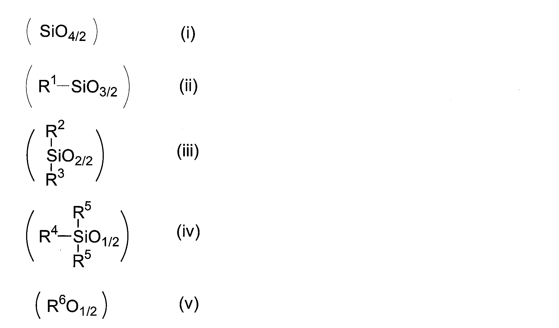
尚、各構造単位の含有割合は、a、w、x、y及びzの規定に基づき、本発明において、上記化合物(A)が全ての構造単位を含まない場合があってもよい。
上記一般式(1)で表される化合物(A)は、(SiO4/2)等で表される構造単位が互いにシロキサン結合で結合したポリシロキサンの1種であり、実際のポリシロキサン分子内の構造単位の結合形態は、必ずしも上記一般式(1)の配列順でなくてもよい。a,w,x,y,zは、それぞれの構造単位の構成比(モル比)を表す。
上記一般式(1)において、R1、R2、R3、R4及びR5のいずれか1つが水素原子であるので、化合物(A)は、化学的反応性を有するSi-H結合を含むことになる。Si-H結合は、Si-H基又はヒドロシリル基と呼ばれることがある。
上記一般式(1)で表される化合物(A)の数平均分子量(Mn)は、好ましくは120以上20000以下、より好ましくは200以上10000以下、更に好ましくは240以上10000以下である。上記範囲のMnを有する化合物(A)を含む表面処理剤を用いると、撥水性の高い皮膜を形成することができ、特に、微細な凹凸表面にも効率よく撥水性皮膜を形成することができる。
上記一般式(1)において、R1、R2、R3、R4及びR5が、互いに独立して、水素原子、アルキル基、アラルキル基、シクロアルキル基又はアリール基である場合、好ましい化合物(A)は、撥水性の観点から、下記一般式(2)~(6)で表される化合物であり、更に好ましい化合物は、一般式(3)及び(4)で表され、特に好ましい化合物は、一般式(4)で表される。一般式(3)で表される化合物は、三官能の、Si-O結合とSi-H結合とを併せ持つ構造単位を有し、一般式(4)で表される化合物は、2つのSi-O結合とSi-H結合とを併せ持つ構造単位を有する。

〔式中、R2、R4及びR5は、互いに独立して、水素原子、アルキル基、アラルキル基、シクロアルキル基又はアリール基であり、R6は、水素原子又は炭素原子数1~6のアルキル基であり、x及びyは正の数であり、zは0又は正の数であり、x/yの比は、好ましくは0.5~2000、更に好ましくは1~200である。〕

〔式中、R5は、互いに独立して、水素原子、アルキル基、アラルキル基、シクロアルキル基又はアリール基であり、R6は、水素原子又は炭素原子数1~6のアルキル基であり、w及びyは正の数であり、zは0又は正の数であり、w/yの比は、好ましくは0.3~5.0である。〕

〔式中、R3及びR5は、互いに独立して、水素原子、アルキル基、アラルキル基、シクロアルキル基又はアリール基であり、R6は、水素原子又は炭素原子数1~6のアルキル基であり、w,x及びyは正の数であり、zは0又は正の数である。〕


上記一般式(4)において、w、x、y及びzの好ましい関係は、これらの合計を1とした場合に、xは、好ましくは0.1~0.9、より好ましくは0.2~0.5、wは、好ましくは0.05~0.5、より好ましくは0.1~0.4、yは、好ましくは0.05~0.5、より好ましくは0.1~0.4、zは、好ましくは0.001~0.2、より好ましくは0.005~0.1である。
本発明において、上記一般式(1)におけるR1、R2、R3、R4及びR5の少なくとも1つがシアノアルキル基である化合物(A)も好ましい態様であり、特に好ましくは、少なくともR1がシアノアルキル基である化合物である。尚、R1、R2、R3、R4及びR5の2つ又はそれ以上がシアノアルキル基である化合物であってもよく、その場合の好ましい例は、例えば、R1及びR5をシアノアルキル基とした化合物である。
シアノアルキル基は、NC-R7-で表される。R7は、炭素原子数1~5の直鎖又は分枝状の2価のアルキル基である。R7の炭素原子数は、好ましくは1~3である。シアノアルキル基の具体例としては、シアノメチル基、シアノエチル基、シアノプロピル基等が例示できる。本発明において、更に好ましくはシアノエチル基又はシアノプロピル基であり、特に好ましくはシアノエチル基である。
シアノアルキル基は、NC-R7-で表される。R7は、炭素原子数1~5の直鎖又は分枝状の2価のアルキル基である。R7の炭素原子数は、好ましくは1~3である。シアノアルキル基の具体例としては、シアノメチル基、シアノエチル基、シアノプロピル基等が例示できる。本発明において、更に好ましくはシアノエチル基又はシアノプロピル基であり、特に好ましくはシアノエチル基である。
上記一般式(1)におけるR1、R2、R3、R4及びR5の少なくとも1つがシアノアルキル基である場合の各構造単位の構成比については、x及びyが共に0でない場合のx/yの比は、好ましくは0.1~200、更に好ましくは0.5~20である。また、w及びyが共に0でない場合のw/yの比は、好ましくは0.3~5.0である。
上記シアノアルキル基を有する化合物(A)のうち、好ましい化合物は、下記一般式(7)で表される。

〔式中、Bはシアノアルキル基であり、R2、R3、R4及びR5は、互いに独立して、水素原子、アルキル基、アラルキル基、シクロアルキル基又はアリール基であり、R6は、水素原子又は炭素原子数1~6のアルキル基であり、b、x、y及びzは、互いに独立して、0又は正の数であり、cは正の数である。〕
上記一般式(7)における(H-SiO3/2)b(B-SiO3/2)cは、上記一般式(1)における(R1-SiO3/2)wに含まれる。即ち、(b+c)=wである。bとcのモル比(b/c)が高いほど、撥水性が高い傾向にあるが、好ましい撥水性のバランスの観点から、好ましくは20~0.1、更に好ましくは10~0.2、特に好ましくは5~0.5の間である。
上記一般式(7)で表される化合物のうち、更に好ましい化合物は、下記一般式(8)で表すことができる。

〔式中、Bはシアノアルキル基であり、R3及びR5は、互いに独立して、アルキル基、アラルキル基、シクロアルキル基又はアリール基であり、R6は、水素原子又は炭素原子数1~6のアルキル基であり、b、x、y及びzは、互いに独立して、0又は正の数であり、cは正の数である。〕
上記一般式(8)で表される化合物もまた、ポリシロキサンの1種である。
上記一般式(1)で表され、シアノアルキル基を有する化合物の他の例は、下記一般式(9)及び(10)で表される。

〔式中、R2、R4及びR5は、互いに独立して、水素原子、シアノアルキル基、アルキル基、アラルキル基、シクロアルキル基又はアリール基であり、R2、R4及びR5のうちの少なくとも1つは、シアノアルキル基であり、R6は、水素原子又は炭素原子数1~6のアルキル基であり、x及びyは正の数であり、zは0又は正の数であり、x/yの比は、好ましくは0.1~200、更に好ましくは0.5~20である。〕

〔式中、1つのR5は、シアノアルキル基であり、他方のR5は、互いに独立して、水素原子、アルキル基、アラルキル基、シクロアルキル基又はアリール基であり、R6は、水素原子又は炭素原子数1~6のアルキル基であり、w及びyは正の数であり、zは0又は正の数であり、w/yの比は、好ましくは0.3~5.0、更に好ましくは0.8~4.0である。〕
上記化合物(A)の製造方法は、特に限定されないが、各構造単位を形成する原料有機ケイ素化合物を、酸性条件下、加水分解縮合に供する方法が一般的である。
上記構造単位(i)を形成する場合には、原料有機ケイ素化合物として、テトラメトキシシラン、テトラエトキシシラン、テトラプロポキシシラン、テトラクロロシラン等を用いることができる。
上記構造単位(ii)を形成する場合には、原料有機ケイ素化合物として、トリメトキシシラン、トリエトキシシラン、トリプロポキシシラン、トリクロロシラン、シアノプロピルトリメトキシシラン、シアノエチルトリエトキシシラン等を用いることができる。
上記構造単位(iii)を形成する場合には、原料有機ケイ素化合物として、ジメトキシメチルシラン、ジエトキシメチルシラン、ジプロポキシメチルシラン、ジクロロメチルシラン等を用いることができる。
上記構造単位(iv)を形成する場合には、原料有機ケイ素化合物として、メトキシトリメチルシラン、クロロトリメチルシラン、トリメチルシラノール、ヘキサメチルジシロキサン、テトラメチルジシロキサン等を用いることができる。
上記構造単位(v)を形成する場合には、メタノール,エタノール、プロパノール、s-ブタノール等を用いることができる。
上記構造単位(i)を形成する場合には、原料有機ケイ素化合物として、テトラメトキシシラン、テトラエトキシシラン、テトラプロポキシシラン、テトラクロロシラン等を用いることができる。
上記構造単位(ii)を形成する場合には、原料有機ケイ素化合物として、トリメトキシシラン、トリエトキシシラン、トリプロポキシシラン、トリクロロシラン、シアノプロピルトリメトキシシラン、シアノエチルトリエトキシシラン等を用いることができる。
上記構造単位(iii)を形成する場合には、原料有機ケイ素化合物として、ジメトキシメチルシラン、ジエトキシメチルシラン、ジプロポキシメチルシラン、ジクロロメチルシラン等を用いることができる。
上記構造単位(iv)を形成する場合には、原料有機ケイ素化合物として、メトキシトリメチルシラン、クロロトリメチルシラン、トリメチルシラノール、ヘキサメチルジシロキサン、テトラメチルジシロキサン等を用いることができる。
上記構造単位(v)を形成する場合には、メタノール,エタノール、プロパノール、s-ブタノール等を用いることができる。
本発明の表面処理剤は、上記化合物(A)を1種のみ含んでよいし、2種以上を含んでもよい。例えば、上記一般式(4)で表される化合物と、上記一般式(7)で表される化合物とを組み合わせてもよい。
本発明の表面処理剤は、上記一般式(1)で表される化合物(A)を含み、この化合物(A)のみからなるものであってよいし、上記化合物(A)と、他の撥水化剤とからなるものであってもよい。他の撥水化剤としては、下記一般式(11)で表される化合物(以下、「化合物(B)」という)が好ましい。

〔式中、R11、R12及びR13は、互いに独立して、水素原子、アルキル基、アラルキル基、シクロアルキル基、シクロアラルキル基又はアリール基であり、R14及びR15は、互いに独立して、水素原子、飽和若しくは不飽和アルキル基、飽和若しくは不飽和シクロアルキル基、トリメチルシリル基、ジメチルシリル基、又は、飽和若しくは不飽和ヘテロシクロアルキル基であり、R14及びR15は、互いに結合して、窒素原子を有する飽和又は不飽和ヘテロシクロアルキル基であってもよい。〕
上記化合物(B)としては、N,N-ジメチルアミノトリメチルシラン(以下、「DMATMS」と略す)、N,N-ジメチルアミノトリエチルシラン、N,N-ジフェニルアミノトリエチルシラン、N,N-ジエチルアミノトリメチルシラン、t-ブチルアミノトリメチルシラン、アリルアミノトリメチルシラン、トリメチルシリルアセタミド、トリメチルシリルピペリジン、トリメチルシリルイミダゾール、トリメチルシリルピロリジン、ヘキサメチルジシラザン、N-メチルヘキサメチルジシラザン、1,2-ジ-N-オクチルテトラメチルジシラザン、1,2-ジビニルテトラメチルジシラザン、ヘプタメチルジシラザン、ノナメチルトリシラザン、トリス(ジメチルシリル)アミン等が挙げられる。これらの化合物は、単独で用いてよいし、2つ以上を組み合わせて用いてもよい。
本発明の表面処理剤が化合物(B)を含む場合、化合物(A)と化合物(B)との含有比率に限定はない。化合物(A)及び化合物(B)の合計を100質量%とした場合、化合物(B)の割合は、好ましくは60質量%未満であり、更に好ましくは1質量%以上40質量%未満である。
本発明の表面処理剤は、更に、有機溶剤、添加剤(pH調整剤、レベリング剤、界面活性剤、シランカップリング剤、安定剤等)を含有してもよい。有機溶剤としては、化合物(A)を溶解する溶剤、又は、化合物(A)を溶解しないが、この化合物(A)と、添加剤等とを分散させる溶剤、を用いることができる。本発明においては、より均一な濃度分布の表面処理剤が得られることから、化合物(A)を溶解可能な化合物が好ましい。また、被処理物、特に、有機液晶や半導体の基板に形成された樹脂パターン又は被エッチングパターンの表面に対するダメージの少ない、従来公知の溶剤を使用することができる。具体的には、ジメチルスルホキシド等のスルホキシド類;ジメチルスルホン、ジエチルスルホン、ビス(2-ヒドロキシエチル)スルホン、テトラメチレンスルホン等のスルホン類;N,N-ジメチルホルムアミド、N-メチルホルムアミド、N,N-ジメチルアセトアミド、N-メチルアセトアミド、N,N-ジエチルアセトアミド等のアミド類;N-メチル-2-ピロリドン、N-エチル-2-ピロリドン、N-プロピル-2-ピロリドン、N-ヒドロキシメチル-2-ピロリドン、N-ヒドロキシエチル-2-ピロリドン等のラクタム類;1,3-ジメチル-2-イミダゾリジノン、1,3-ジエチル-2-イミダゾリジノン、1,3-ジイソプロピル-2-イミダゾリジノン等のイミダゾリジノン類;ジメチルエーテル、ジエチルエーテル、メチルエチルエーテル、ジプロピルエーテル、ジイソプロピルエーテル、ジブチルエーテル等のジアルキルエーテル類;ジメチルグリコール、ジメチルジグリコール、ジメチルトリグリコール、メチルエチルジグリコール、ジエチルグリコール等のジアルキルグリコールエーテル類;プロピレングリコールモノメチルエーテル等のアルキレングリコールモノアルキルエーテル類;プロピレングリコールモノメチルエーテルアセテート,酢酸エチル,酢酸ブチル等のエステル類;メチルエチルケトン、シクロヘキサノン、2-ヘプタノン、3-ヘプタノン等のケトン類;p-メンタン、ジフェニルメンタン、リモネン、テルピネン、ボルナン、ノルボルナン、ピナン等のテルペン類;直鎖状、分枝状、又は環状の炭化水素系溶剤、芳香族炭化水素系溶剤、等が挙げられる。これらの有機溶剤は、単独で用いても2種以上組み合わせて用いてもよい。
これらの有機溶剤のうち、極性が比較的小さく、分子量の小さなものが好ましい。しかしながら、分子量が小さすぎると揮発性が高すぎて取り扱いが難しくなる。そこで、好ましい有機溶剤としては、炭素原子数6~12の直鎖状若しくは分枝状の炭化水素系溶剤又はテルペン系溶剤であり、具体的には、n-ヘキサン、n-ヘプタン、n-オクタン、n-ノナン、メチルオクタン、n-デカン、n-ウンデカン、n-ドデカン等が挙げられる。また、テルペン系溶剤としては、p-メンタン、o-メンタン、m-メンタン等のメンタン、ジフェニルメンタン、リモネン、α-テルピネン、β-テルピネン、γ-テルピネン等のテルピネン、ボルナン、ノルボルナン、ピナン、α-ピネン、β-ピネン等のピネン、カラン、ロンギホレン等のモノテルペン類、アビエタン等のジテルペン類、等が挙げられる。これらの有機溶剤は、単独で用いてよいし、2種以上を組み合わせて用いてもよい。より好ましい有機溶剤は、炭素原子数7~10の直鎖状の炭化水素系溶剤、メンタン及びピナンであり、特に好ましくはヘキサン及びオクタンである。
本発明の表面処理剤が有機溶剤を含有する場合、化合物(A)の濃度、又は、化合物(A)及び他の撥水化剤の合計量の濃度は、表面処理剤の全量に対して、好ましくは0.1~60%であり、更に好ましくは0.5~30%、より好ましくは1~20%である。
本発明の表面処理剤を用いて、被処理物の表面の撥水化に好適な基板としては、Si、SiO2、SiON、SiN、p-Si、α-Si、W、W-Si、Al、Cu、Al-Si、Si-C、アルミナ、サファイア、ガラス、樹脂等からなる基板が挙げられる。また、上記の材質からなる基板に限らず、基部の表面に、Si、SiO2、SiON、SiN、p-Si、α-Si、W、W-Si、Al、Cu、Al-Si、アルミナ、サファイア、ITO、ZnO、ガラス等からなる膜を有する積層型基板の膜に対しても、同様に撥水化することができる。
上記の膜は、CVD、真空蒸着、メッキ、鍍金等の従来公知の技術を用いて形成されたものである。CVDには、プラズマCVD、熱CVD、光CVD等の方法が知られているが、いずれの方法で形成した膜であってもよい。より具体的には、SiO2、SiON、SiN、Si等の膜の製造方法としては、プラズマ等の低温成膜技術や高温でエピタキシャル成長させる方法等、多種が知られている。例えば、SiNは、必ずしも化学量論値であるSi3N4の組成ではなく、SiNxと表記される中間組成であることはよく知られている。本発明では、いずれの組成でも効果を奏するので、代表して、SiN(又は窒化ケイ素)と称する。
本発明において、好ましい被処理物は、接触角が好ましくは0~80度、より好ましくは5~60度、更に好ましくは10~50度の材質を表面に有する。特に好ましくは、シリコンウェハを用いた半導体基板であり、その表面に、SiN、SiO2、金属ケイ素(Si)等(Si-OHを有する場合を含む)の膜やパターンが載っていてもよく、レジスト樹脂の膜やそのパターンが載っていてもよい。本発明の効果が最も著しいのは、基板の表面の少なくとも一部に、Si3N4やSiON等のSiN、SiO2、並びに、非晶質シリコン及び結晶質シリコン等のSiの3種類の材質のうち、少なくとも2種を有する基板であり、更に好ましくは、これら3種類の材質を有する基板である。
本発明の表面処理剤によれば、被処理物の表面の材質に関わらず高い撥水性皮膜を与えることができる。表面にSi-OHを有するシリコンウェハの場合において、化合物(A)におけるSi-H結合は、H原子が負に、Si原子が正に分極しており、シリコンウェハ表面のSi-OH基のO-H結合において、O原子が負に、H原子が正に分極していることと正反対なため、ここで水素結合を生じ、化合物(A)が基板表面に配向して基板表面に撥水性を与える効果を生じているものと考えられる。
特に、本発明の表面処理剤が、上記一般式(1)においてR1、R2、R3、R4及びR5の少なくとも1つがシアノアルキル基である化合物(A)を含む場合には、SiO2、SiN、及びSiのいずれに対しても高い撥水性皮膜を与えることできる。更に、化合物(A)がシアノアルキル基を含む場合に、シアノアルキル基の量及びSi-H結合の量によって、それぞれの表面材質に対する効果の大きさを制御することができる。即ち、シアノアルキル基を有する構造単位の合計量、及び、Si-H結合を有する構造単位の合計量の割合を、両者の合計を100モル%とした場合に、それぞれ、1~20モル%及び99~80モル%とするものである。一つの構造単位がシアノアルキル基とSi-H結合の両方を有する場合は、シアノアルキル基に着目したシアノアルキル基を有する構造単位の量と、Si-H結合に着目したSi-H結合を有する構造単位の量として、両者の合計を100モル%として計算を行えば、上記の制御を同様にすることができる。このような制御によって、SiO2、SiN、及びSiの異なる材質の表面における各接触角の値を近づけることができる。最新の液晶や半導体の基板表面では、SiO2、SiN、Si等の様々な表面材質の微小パターンが併存しているので、単に基板表面を撥水化できるだけでなく、異なる材質の表面に同程度の撥水性を付与できることは、複雑なパターンを有する半導体等の基板表面でのパターン倒れの問題を解決する上で極めて有利な効果である。このような効果は、従来知られていなかったものである。
本発明の表面処理方法は、上記本発明の表面処理剤を、被処理物の表面に接触させる接触工程を備える。
接触工程の具体的な方法は、特に限定されるものではないが、表面処理剤を塗布する方法が簡便である。塗布は、スプレー塗布や回転塗布、ディッピング等のどんな方法でもよいが、薄く均一な撥水性皮膜が得られるという観点から、回転塗布が好ましい。また、表面処理剤は、有機溶剤を含有するものが好ましく用いられる。
接触工程の具体的な方法は、特に限定されるものではないが、表面処理剤を塗布する方法が簡便である。塗布は、スプレー塗布や回転塗布、ディッピング等のどんな方法でもよいが、薄く均一な撥水性皮膜が得られるという観点から、回転塗布が好ましい。また、表面処理剤は、有機溶剤を含有するものが好ましく用いられる。
本発明の表面処理剤が、上記化合物(A)及び化合物(B)を含有する場合には、塗膜の厚さの均一性の観点から、これらが混合された状態で用いるのが好ましいが、上記化合物(A)及び化合物(B)のいずれか一方を先に半導体基板の表面に接触させてから他方を接触させる方法や、別々の供給口から化合物(A)及び化合物(B)の両方を同時に半導体基板の表面に供給する方法等も用いることができる。
本発明において、被処理物は、その表面の一部に、SiO2、SiN及びSiの少なくとも1種からなる膜を有する半導体基板であることが好ましい。
接触工程の前に、半導体基板の洗浄、乾燥等の前処理を行ってもよく、接触工程の後に、洗浄や乾燥等の後処理を行ってもよい。しかしながら、前処理に用いた洗浄液が乾燥する際の表面張力によって、パターン倒れが引き起こされるメカニズムを考慮すると、前処理に乾燥工程を備えるのは好ましくなく、前処理用洗浄液による洗浄後、乾燥することなく、本発明の表面処理剤を用いて接触工程を行うことが好ましい。
接触工程の前に、半導体基板の洗浄、乾燥等の前処理を行ってもよく、接触工程の後に、洗浄や乾燥等の後処理を行ってもよい。しかしながら、前処理に用いた洗浄液が乾燥する際の表面張力によって、パターン倒れが引き起こされるメカニズムを考慮すると、前処理に乾燥工程を備えるのは好ましくなく、前処理用洗浄液による洗浄後、乾燥することなく、本発明の表面処理剤を用いて接触工程を行うことが好ましい。
前処理工程における洗浄方法としては、特に限定されないが、例えば、アンモニア及び過酸化水素を用いる「SC1洗浄」と呼ばれる方法が知られている。また、半導体基板の洗浄の前後に、表面の酸処理(以下、「酸接触工程」という)を行ってもよい。
上記酸接触工程は、具体的には、塗布、スプレー、浸漬、蒸気接触等の方法で、半導体基板の表面に、酸を含む酸性液体を接触させることである。本発明においては、酸の水溶液に基板を浸漬する方法が、簡便な装置で実施できるので好ましい。酸性液体として水溶液を用いる場合の酸の濃度は、好ましくは0.1質量%以上96質量%以下、更に好ましくは1質量%以上30質量%以下、より好ましくは5質量%以上20質量%以下である。
半導体基板の表面に酸性液体を接触させる条件は、特に限定されないが、好ましくは0℃より高く70℃以下の温度で、1秒~30分程度、更に好ましくは10秒~10分間接触させることで、不純物除去等の効果を得ることができる。
半導体基板の表面に酸性液体を接触させる条件は、特に限定されないが、好ましくは0℃より高く70℃以下の温度で、1秒~30分程度、更に好ましくは10秒~10分間接触させることで、不純物除去等の効果を得ることができる。
上記酸接触工程で用いる酸は、有機酸、無機酸のいずれでもよい。有機酸の場合はシュウ酸やトリクロロ酢酸、トリフルオロ酢酸、ジクロロ酢酸等、2.0以下の酸解離定数(pKa)を有する酸が好ましく、シュウ酸が更に好ましい。無機酸の場合は0.0以下の酸解離定数(pKa)を有する無機酸が好ましく、具体的には、塩酸、硫酸、硝酸、ヨウ化水素酸、臭化水素酸、塩素酸、臭素酸、ヨウ素酸、過マンガン酸、チオシアン酸、過塩素酸、過臭素酸、テトラフルオロホウ酸、ヘキサフルオロリン酸等が挙げられる。これらのうち、工業的に得やすい塩酸、硫酸及び硝酸が好ましく、酸化性がない点で安全であり、難溶性塩を生じにくい点で、塩酸が特に好ましい。有機酸と無機酸とでは、高純度品が得やすい点で無機酸の方が好ましい。これらの酸は、市販されている程度で高純度のものが好ましい。また、半導体用途で用いるために、パーティクルを除いたELグレードと呼ばれるものも同様に好ましく用いることができる。
更に、シュウ酸等の水溶性の低い酸では、2-プロパノールやメチルエチルケトン等を有機溶媒とした溶液を、他の酸水溶液と同様に用いることができる。
更に、シュウ酸等の水溶性の低い酸では、2-プロパノールやメチルエチルケトン等を有機溶媒とした溶液を、他の酸水溶液と同様に用いることができる。
本発明の表面処理剤に含まれる化合物(A)は、水と接触して加水分解することがあり、また、表面処理剤が有機溶剤を含む場合の好ましい溶剤は、極性が比較的小さいものであるので、前処理工程における洗浄や、洗浄後の酸接触工程で水を用いた場合は、洗浄工程と酸接触工程との間、並びに、酸接触工程と接触工程との間において、水及び表面処理剤に含まれる有機溶剤の中間の極性を有する、例えば、アルコールのような有機溶剤を用いて、半導体基板の表面に残存した媒体を置換する工程を備えることが好ましい。
また、接触工程の後は、通常、乾燥が行われるが、半導体基板の表面に過剰の表面処理剤が残っていると、基板表面に斑を生じる可能性がある。そこで、極性が比較的小さな有機溶剤を含む表面処理剤を半導体基板表面に接触させた後、水及び表面処理剤に含まれていた有機溶剤の中間の極性を有する、例えば、アルコールのような有機溶剤を用いて、半導体基板の表面に残存した媒体を置換する工程を行い、その後、水で洗浄することが好ましい。本発明の表面処理剤により撥水化が行われた基板表面では、上記の置換工程や洗浄工程を行った後でも、優れた撥水性を保ち、更に乾燥工程を行っても、パターン倒れを抑えることができる。その後の半導体製造工程において、基板表面を親水化する場合には、ドライアッシングやオゾン酸化処理、湿式酸化等の処理を行うことができる。
本発明の表面処理方法における一形態としての、本発明の表面処理剤を用いた基板表面の具体的処理方法としては、脱イオン水を用いた洗浄方法によって基板を洗浄した後、水洗し、アルコールによる溶剤置換を行い、表面処理剤との接触工程として、低極性溶剤で希釈した表面処理剤を基板に接触させ、その後、アルコールによる溶剤置換をした後、脱イオン水で洗浄した後に乾燥する一連の工程を挙げることができる。
本発明の表面処理方法における別の一形態としての、本発明の表面処理剤を用いた基板表面の具体的処理方法としては、脱イオン水を用いた洗浄方法によって基板を洗浄した後、酸を含む水溶液に浸漬し、水洗し、アルコールによる溶剤置換を行い、表面処理剤との接触工程として、低極性溶剤で希釈した表面処理剤を基板に接触させ、その後、アルコールによる溶剤置換をした後、脱イオン水で洗浄した後に乾燥する一連の工程を挙げることができる。
本発明の表面処理方法において、表面処理剤が化合物(A)を主とする場合、形成される撥水性皮膜の主な構成材料は、化合物(A)そのものであるか、あるいは、化合物(A)に含まれる官能基と、被処理物の表面を構成する材質に含まれる官能基とが反応して得られたケイ素化合物である。この撥水性皮膜における接触角は、好ましくは80~120度、より好ましくは85~95度である。
また、本発明の表面処理方法において、表面処理剤が化合物(A)及び(B)を含む場合、形成される撥水性皮膜の主な構成材料は、化合物(A)及び化合物(B)そのものであるか、化合物(A)及び化合物(B)が縮合して形成されたケイ素化合物、あるいは、化合物(A)に含まれる官能基及び/又は化合物(B)に含まれる官能基と、被処理物の表面を構成する材質に含まれる官能基とが反応して得られたケイ素化合物である。この撥水性皮膜における接触角は、好ましくは80~120度、より好ましくは85~95度である。
また、本発明の表面処理方法において、表面処理剤が化合物(A)及び(B)を含む場合、形成される撥水性皮膜の主な構成材料は、化合物(A)及び化合物(B)そのものであるか、化合物(A)及び化合物(B)が縮合して形成されたケイ素化合物、あるいは、化合物(A)に含まれる官能基及び/又は化合物(B)に含まれる官能基と、被処理物の表面を構成する材質に含まれる官能基とが反応して得られたケイ素化合物である。この撥水性皮膜における接触角は、好ましくは80~120度、より好ましくは85~95度である。
上記被処理物が、その表面に窒化ケイ素膜と酸化ケイ素膜とを有するシリコンウェハ(半導体基板)等であった場合には、上記接触工程の後、窒化ケイ素膜の表面における接触角(Can)と、酸化ケイ素膜の表面における接触角(Cao)との比(Can/Cao)を、好ましくは0.7~1.3の範囲、より好ましくは0.9~1.1、特に好ましくは0.97~1.03とすることができる。
他の本発明は、半導体基板の表面の撥水化を行う表面処理方法であって、酸を含む酸性液体を上記半導体基板に接触させる第1工程と、下記一般式(11)で表される化合物(B)を含有する表面処理剤を上記半導体基板に接触させる第2工程とを、順次、備えることを特徴とする表面処理方法である。尚、半導体基板は、接触角が好ましくは0~80度、より好ましくは5~60度、更に好ましくは10~50度の材質を表面に有する、シリコンウェハを意味し、その表面に、SiN、SiO2、(Si)等(Si-OHを有する場合を含む)の膜やパターンが載っていてもよく、レジスト樹脂の膜やそのパターンが載っていてもよい。

〔式中、R11、R12及びR13は、互いに独立して、水素原子、アルキル基、アラルキル基、シクロアルキル基、シクロアラルキル基又はアリール基であり、R14及びR15は、互いに独立して、水素原子、飽和若しくは不飽和アルキル基、飽和若しくは不飽和シクロアルキル基、トリメチルシリル基、ジメチルシリル基、又は、飽和若しくは不飽和ヘテロシクロアルキル基であり、R14及びR15は、互いに結合して、窒素原子を有する飽和又は不飽和ヘテロシクロアルキル基であってもよい。〕
第1工程である、半導体基板表面に酸性液体を接触させる工程を行う前に、基板表面の洗浄をすることができる。洗浄方法としては、例えば、アンモニアと過酸化水素を用いる「SC1洗浄」や、塩酸と過酸化水素を用いる、「SC2洗浄」と呼ばれる方法が知られている他、公知の洗浄方法ならばいずれでも用いることができる。しかし、例えば、フッ酸と硝酸の混合物を用いるような洗浄方法では半導体基板表面が浸食されてしまうことは明らかであり、パターンの形成された後の表面に適用するのが好ましくないことは言うまでもない。
また、SC1洗浄液はアルカリ性であるから、洗浄した後は、本発明において、半導体基板表面に酸性液体を接触させる工程を行う前に水洗工程を行うことが好ましい。同様に、SC2洗浄をした後も、水洗をするのが好ましい。本発明で用いる酸性液体とSC2洗浄で用いる塩酸と過酸化水素を共存させた洗浄液とは過酸化水素の有無が異なり、酸性液体を接触させる工程の代わりにSC2洗浄を行っても、本発明の効果は得られない。
また、第2工程で用いる化合物(B)は加水分解する場合があり、また、表面処理剤を溶剤希釈して用いる場合の好ましい溶剤は、比較的極性が小さいものであるので、第1工程の後は、水洗浄を行い、更に、水と第2工程で用いる溶剤の中間の極性を有する例えばアルコールのような溶剤を用いて溶剤置換する工程を挟むことが好ましい。
第2工程において、基板に表面処理剤を接触させる方法としては、特に限定されるものではないが、表面処理剤を塗布する方法が簡便である。塗布はスプレー塗布や回転塗布、ディッピング等のどんな方法でもよいが、薄く均一な処理膜が得られるという点は回転塗布が好ましい。また、表面処理剤は溶剤で希釈したものが好ましく用いられる。
表面処理を行う前に、基板の洗浄、乾燥等の前処理を行っても良く、表面処理の後でも、洗浄や乾燥等の後処理をすることもできるが、洗浄液が乾燥する際の表面張力によってパターン倒れが引き起こされるメカニズムを考慮すると、前処理に乾燥工程を挟むのは好ましくなく、洗浄液による洗浄後、乾燥することなく本発明で用いる表面処理剤を用いて表面処理を行うのが好ましい。
また、表面処理剤と接触させる工程の後は、通常、乾燥工程が含まれ、乾燥工程でパターン倒れが起きないことが本願発明の効果であるが、乾燥工程の前に過剰の表面処理剤が多量に残っていると、基板表面に斑を生じたりする可能性があるので、好ましいのは、極性が比較的小さな溶剤で希釈した表面処理剤と基板表面を接触させた後、水と表面処理で用いた溶剤の中間の極性を有する例えばアルコールのような溶剤を用いて溶剤置換する工程を挟み、水で洗浄することが好ましい。本発明の表面処理が行われた基板表面では、上記の溶剤置換や洗浄を行った後でも撥水性を保ち、乾燥を行ってもパターン倒れを抑えることができる。その後の半導体製造工程において、基板表面を親水化したい場合にはドライアッシングやオゾン酸化処理、湿式酸化等の処理を行うことができる。
本発明の一形態としての、半導体基板表面の具体的処理方法としては、脱イオン水を用いた洗浄方法によって基板を洗浄した後、酸性液体を含む水溶液に浸漬し(第1工程)、水洗し、アルコールによる溶剤置換を行い、化合物(B)を含む表面処理剤との接触工程(第2工程)として、低極性溶剤で希釈した表面処理剤を基板に接触させ、その後、アルコールによる溶剤をした後、脱イオン水で洗浄した後に乾燥する一連の工程を挙げることができる。
シリコンウェハの洗浄方法として、フッ酸/硝酸や塩酸/過酸化水素等を用いる方法が知られているが、これらは基板表面の酸化膜や金属を溶去する作用があるのに比べて、本発明において酸を用いる意味はまったく異なる。基板表面には酸性のSi-OH基が存在することは知られており、従来公知のシリル化剤は表面のSi-OH基と反応して表面を撥水化すると言われてきたが、窒化ケイ素表面において、この効果が十分現れないことは、特許文献3で開示されているとおりである。本発明者らは、窒化ケイ素表面で効果が現れない理由は、基板表面に塩基性を帯びた官能基があるためではないかと考え、基板表面を酸性に変える目的で、過酸化水素を共存させずに酸を接触させ、その後、特定の撥水化剤を含む表面処理剤で表面処理をしてみたところ、優れた効果を見出して本願発明を完成させたものである。
以下、本発明を実施例により具体的に説明する。但し、本発明は、この実施例に何ら限定されるものではない。
本発明に係る化合物(A)等のポリシロキサンの数平均分子量は、GPC装置として、東ソー社製高速GPCシステム「HLC-8320GPC」(型式名)により測定した。カラムは、東ソー社製「TSKgel G4000HXL」及び「TSKgel G2000HXL」を連結して用いた。
また、ポリシロキサンの粘度は、E型粘度計により測定した。
また、ポリシロキサンの粘度は、E型粘度計により測定した。
表面処理剤の調製に用いた他の化合物は、以下に示される。
(1)DMATMS
東京化成社製N,N-ジメチルアミノトリメチルシランである。
(2)HMDS
キシダ化学社製1,1,1,3,3,3-ヘキサメチルジシラザンである。
(3)TMCT
アルファーエイザー社製2,4,6,8-テトラメチルシクロテトラシロキサンである。
(4)OMCT
東京化成社製オクタメチルシクロテトラシロキサンであり、Si-H結合を有さない化合物である。
(5)KF-96
信越シリコーン社製ジメチルシリコーンオイル「KF-96-30cs」(商品名)であり、一般式(1)におけるzが0の、Si-H結合を有さない化合物である。
(6)KF-99
信越シリコーン社製ハイドロジェンシリコーンオイル「KF-99」(商品名)であり、一般式(1)におけるa、w及びzがすべて0の化合物である。
(7)Q-2
Mayaterials Inc.社製オクタ(ヒドロジメチルシロキシ)シルセスキオキサンである。
(8)n-オクタン
(1)DMATMS
東京化成社製N,N-ジメチルアミノトリメチルシランである。
(2)HMDS
キシダ化学社製1,1,1,3,3,3-ヘキサメチルジシラザンである。
(3)TMCT
アルファーエイザー社製2,4,6,8-テトラメチルシクロテトラシロキサンである。
(4)OMCT
東京化成社製オクタメチルシクロテトラシロキサンであり、Si-H結合を有さない化合物である。
(5)KF-96
信越シリコーン社製ジメチルシリコーンオイル「KF-96-30cs」(商品名)であり、一般式(1)におけるzが0の、Si-H結合を有さない化合物である。
(6)KF-99
信越シリコーン社製ハイドロジェンシリコーンオイル「KF-99」(商品名)であり、一般式(1)におけるa、w及びzがすべて0の化合物である。
(7)Q-2
Mayaterials Inc.社製オクタ(ヒドロジメチルシロキシ)シルセスキオキサンである。
(8)n-オクタン
合成例1-1
本発明に係る化合物(A)の製造方法を記載する。
300ml四つ口フラスコに、磁気回転子、送液ポンプ、還流冷却器及び温度計を装着し、系内を窒素ガスで置換した。このフラスコに、トリエトキシシラン8.21g(50mmol)、2-シアノエチルトリエトキシシラン10.87g(50mmol)、ジメトキシメチルシラン10.62g(100mmol)、1,1,3,3-テトラメチルジシロキサン20.15g(150mmol)、2-ブタノール24.71g及びキシレン74.12gを収容し、反応系を窒素ガス雰囲気にした。フラスコ内の温度を25℃に保ち、3.14%塩酸水溶液9.30g及び2-ブタノール12.35gの混合液を、滴下ロートから徐々に加えながら撹拌した。滴下終了後、反応液を25℃で22時間静置した。
本発明に係る化合物(A)の製造方法を記載する。
300ml四つ口フラスコに、磁気回転子、送液ポンプ、還流冷却器及び温度計を装着し、系内を窒素ガスで置換した。このフラスコに、トリエトキシシラン8.21g(50mmol)、2-シアノエチルトリエトキシシラン10.87g(50mmol)、ジメトキシメチルシラン10.62g(100mmol)、1,1,3,3-テトラメチルジシロキサン20.15g(150mmol)、2-ブタノール24.71g及びキシレン74.12gを収容し、反応系を窒素ガス雰囲気にした。フラスコ内の温度を25℃に保ち、3.14%塩酸水溶液9.30g及び2-ブタノール12.35gの混合液を、滴下ロートから徐々に加えながら撹拌した。滴下終了後、反応液を25℃で22時間静置した。
次いで、反応液を蒸留装置内に配置し、到達圧力133Paまで減圧した状態で、反応液の温度を16℃から60℃まで上昇させて水を含む揮発性成分を減圧留去した。そして、無色の液体(以下、「ポリシロキサン(PCN1)」という。)21.4gを得た。このポリシロキサン(PCN1)について、GPCにより、数平均分子量(Mn)を測定したところ、600であった。また、25℃における粘度を測定したところ、7mPa・sであった。
ポリシロキサン(PCN1)の組成を、構造単位のモル比とともに、下記構造式(12)に示す。

(CNはシアノ基、Meはメチル基、s-Buはセカンダリーブチル基、Etはエチル基を示す。)
組成は、ポリシロキサン(PCN1)を、CDCl3(重クロロホルム)溶媒とした、1H-NMR(プロトン核磁気共鳴)及び29Si-NMRの測定に供し、得られたケミカルシフトから解析した。すなわち、1H-NMRスペクトルにおけるケミカルシフトδ(ppm)が2.2~2.5のシグナルは、(CH2CH2CN)に由来し、δ(ppm)が3.6~3.8のシグナルは、(OCH2CH3)、δ(ppm)が3.8~4.1のシグナルは、(OCH(CH3)CH2CH3)に由来する。更に、29Si-NMRスペクトルより、δ(ppm)が-10~0のシグナルは、SiO1/2の構造に由来し、δ(ppm)が-40~-35のシグナルは、SiO2/2の構造に由来する。SiO1.5あるいはSiO3/2として表記される、Si-O-結合を3つ有する構造を与える原料化合物(Tモノマーと呼ばれる)、及び、SiO1.0あるいはSiO2/2として表記される、Si-O-結合を2つ有する構造を与える原料化合物(Dモノマーと呼ばれる)については、縮合反応において仕込んだ原料化合物が、ほぼその使用量の割合でポリシロキサンに組み込まれることが分かっている。そこで、各々のシグナル強度積分値から、側鎖に関する連立方程式を作製し、各モノマーの仕込み量と、NMRの積分値とから、ポリシロキサン(PCN1)に含まれる各構成単位のモル比を決定した。
合成例1-2
300ml四つ口フラスコに、磁気回転子、送液ポンプ、還流冷却器及び温度計を装着し、系内を窒素ガスで置換した。このフラスコに、トリエトキシシラン12.32g(75mmol)、2-シアノエチルトリエトキシシラン5.43g(25mmol)、ジメトキシメチルシラン10.62g(100mmol)、1,1,3,3-テトラメチルジシロキサン20.15g(150mmol)、2-ブタノール24.71g及びキシレン74.12gを収容し、反応系を窒素ガス雰囲気にした。フラスコ内の温度を25℃に保ち、3.14%塩酸水溶液9.30g及び2-ブタノール12.35gの混合液を、滴下ロートから徐々に加えながら撹拌した。滴下終了後、反応液を25℃で22時間静置した。
300ml四つ口フラスコに、磁気回転子、送液ポンプ、還流冷却器及び温度計を装着し、系内を窒素ガスで置換した。このフラスコに、トリエトキシシラン12.32g(75mmol)、2-シアノエチルトリエトキシシラン5.43g(25mmol)、ジメトキシメチルシラン10.62g(100mmol)、1,1,3,3-テトラメチルジシロキサン20.15g(150mmol)、2-ブタノール24.71g及びキシレン74.12gを収容し、反応系を窒素ガス雰囲気にした。フラスコ内の温度を25℃に保ち、3.14%塩酸水溶液9.30g及び2-ブタノール12.35gの混合液を、滴下ロートから徐々に加えながら撹拌した。滴下終了後、反応液を25℃で22時間静置した。
次いで、反応液を蒸留装置内に配置し、到達圧力133Paまで減圧した状態で、反応液の温度を17℃から60℃まで上昇させて水を含む揮発性成分を減圧留去した。そして、無色の液体(以下、「ポリシロキサン(PCN2)」という。)23.97gを得た。このポリシロキサン(PCN2)について、GPCにより、数平均分子量(Mn)を測定したところ、730であった。また、25℃における粘度を測定したところ、6mPa・sであった。
ポリシロキサン(PCN2)の組成を、構造単位のモル比とともに、下記構造式(13)に示す。

(CNはシアノ基、Meはメチル基、s-Buはセカンダリーブチル基、Etはエチル基を示す。)
合成例1-3
300ml四つ口フラスコに、磁気回転子、送液ポンプ、還流冷却器及び温度計を装着し、系内を窒素ガスで置換した。このフラスコに、トリエトキシシラン32.85g(200mmol)、1,1,3,3-テトラメチルジシロキサン20.15g(150mmol)、2-プロパノール24.04g及びキシレン72.12gを収容し、反応系を窒素ガス雰囲気にした。フラスコ内の温度を25℃に保ち、2.63%塩酸水溶液11.10g及び2-プロパノール12.02gの混合液を、滴下ロートから徐々に加えながら撹拌した。滴下終了後、反応液を25℃で22時間静置した。
300ml四つ口フラスコに、磁気回転子、送液ポンプ、還流冷却器及び温度計を装着し、系内を窒素ガスで置換した。このフラスコに、トリエトキシシラン32.85g(200mmol)、1,1,3,3-テトラメチルジシロキサン20.15g(150mmol)、2-プロパノール24.04g及びキシレン72.12gを収容し、反応系を窒素ガス雰囲気にした。フラスコ内の温度を25℃に保ち、2.63%塩酸水溶液11.10g及び2-プロパノール12.02gの混合液を、滴下ロートから徐々に加えながら撹拌した。滴下終了後、反応液を25℃で22時間静置した。
次いで、反応液を蒸留装置内に配置し、到達圧力1mmHgまで減圧した状態で、反応液の温度を9℃から60℃まで上昇させて水を含む揮発性成分を減圧留去した。そして、無色の液体(以下、「ポリシロキサン(P1)」という。)19.3gを得た。このポリシロキサン(P1)について、GPCにより、数平均分子量(Mn)を測定したところ、1,050であった。また、25℃における粘度を測定したところ、7mPa・sであった。
ポリシロキサン(P1)の組成を、構造単位のモル比とともに、下記構造式(14)に示す。

(Meはメチル基、i-Prはイソプロピル基、Etはエチル基を示す。)
組成は、ポリシロキサン(P1)を、CDCl3(重クロロホルム)溶媒とした、1H-NMR(プロトン核磁気共鳴)の測定に供し、得られたケミカルシフトから解析した。すなわち、1H-NMRスペクトルにおけるケミカルシフトδ(ppm)が-0.2~0.6のシグナルは、Si-CH3の構造に基づき、δ(ppm)が0.9~1.5のシグナルは、(OCH(CH3)2、及びOCH2CH3)、δ(ppm)が3.5~4.1のシグナルは、OCH2CH3、δ(ppm)が4.1~5.5のシグナルは、OCH(CH3)2及びSi-Hに基づくと考えられる。SiO1.5あるいはSiO3/2で表記される、Si-O-結合を3つ有する構造を与える原料化合物(Tモノマーと呼ばれる)、及び、SiO1.0あるいはSiO2/2として表記される、Si-O-結合を2つ有する構造を与える原料化合物(Dモノマーと呼ばれる)については、縮合反応において仕込んだ原料化合物が、ほぼその使用量の割合でポリシロキサンに組み込まれることが分かっている。そこで、各々のシグナル強度積分値から、側鎖に関する連立方程式を作製し、各モノマーの仕込み量と、NMRの積分値とから、ポリシロキサン(P1)に含まれる各構成単位のモル比を決定した。
合成例1-4
300ml四つ口フラスコに、磁気回転子、送液ポンプ、還流冷却器及び温度計を装着し、系内を窒素ガスで置換した。このフラスコに、トリエトキシシラン16.43g(100mmol)、ジメトキシメチルシラン10.62g(100mmol)、1,1,3,3-テトラメチルジシロキサン20.15g(150mmol)、2-プロパノール20.03g及びキシレン60.10gを収容し、反応系を窒素ガス雰囲気にした。フラスコ内の温度を25℃に保ち、3.14%塩酸水溶液9.30g及び2-プロパノール10.02gの混合液を、滴下ロートから徐々に加えながら撹拌した。滴下終了後、反応液を25℃で22時間静置した。
300ml四つ口フラスコに、磁気回転子、送液ポンプ、還流冷却器及び温度計を装着し、系内を窒素ガスで置換した。このフラスコに、トリエトキシシラン16.43g(100mmol)、ジメトキシメチルシラン10.62g(100mmol)、1,1,3,3-テトラメチルジシロキサン20.15g(150mmol)、2-プロパノール20.03g及びキシレン60.10gを収容し、反応系を窒素ガス雰囲気にした。フラスコ内の温度を25℃に保ち、3.14%塩酸水溶液9.30g及び2-プロパノール10.02gの混合液を、滴下ロートから徐々に加えながら撹拌した。滴下終了後、反応液を25℃で22時間静置した。
次いで、反応液を蒸留装置内に配置し、到達圧力133Paまで減圧した状態で、反応液の温度を7℃から60℃まで上昇させて水を含む揮発性成分を減圧留去した。そして、無色の液体(以下、「ポリシロキサン(P2)」という。)15.6gを得た。このポリシロキサン(P2)について、GPCにより、数平均分子量(Mn)を測定したところ、1,000であった。また、25℃における粘度を測定したところ、3mPa・sであった。
ポリシロキサン(P2)の組成を、構造単位のモル比とともに、下記構造式(15)に示す。

(Meはメチル基、Etはエチル基、i-Prはイソプロピル基を表す。)
組成は、ポリシロキサン(P2)を、CDCl3(重クロロホルム)溶媒とした、1H-NMR(プロトン核磁気共鳴)の測定に供し、得られたケミカルシフトから解析した。すなわち、1H-NMRスペクトルにおけるケミカルシフトδ(ppm)が-0.2~0.6のシグナルは、Si-CH3の構造に基づき、δ(ppm)が0.9~1.5のシグナルは、(OCH(CH3)2、及びOCH2CH3)、δ(ppm)が3.5~4.1のシグナルは、OCH2CH3、δ(ppm)が4.1~5.5のシグナルは、OCH(CH3)2及びSi-Hに基づくと考えられる。また、SiO1.5あるいはSiO3/2で表記される、Si-O-結合を3つ有する構造を与える原料化合物(Tモノマーと呼ばれる)については、仕込んだ原料化合物が、ほぼその使用量の割合でポリシロキサンに組み込まれることが分かっている。そこで、各々のシグナル強度積分値から、側鎖に関する連立方程式を作製し、各モノマーの仕込み量と、NMRの積分値とから、ポリシロキサン(P2)に含まれる各構成単位のモル比を決定した。
実験例1-1
合成例1-2で得られたポリシロキサン(PCN2)2.0質量部と、N,N-ジメチルアミノトリメチルシラン(DMATMS)8.0質量部と、n-オクタン90.0質量部とを混合して、表面処理剤を調製した(表1参照)。この表面処理剤を含む薬液を用いて、被処理物の表面処理を行った。表2に、表面処理の具体的な方法を示す。被処理物(以下、「基板」という)は、10mm×50mmの大きさに切断した窒化ケイ素膜付シリコンウェハ(以下、「SiN基板」と示す場合がある)、酸化ケイ素膜付シリコンウェハ(以下、「SiO2基板」と示す場合がある)及びシリコンウェハ(以下、「Si基板」と示す場合がある)の3種である。基板を、表2のNo.1-1からNo.1-12の順に、樹脂製のカップに秤取った各薬液(約5ml)に、所定の温度で所定時間浸漬させた後、20秒間窒素ガスをブローして水を除去し、速やかに接触角を測定した。尚、被処理物がSiO2基板の場合は、酸化膜が溶けてなくなってしまわないように、No.1-4における処理において、1%HF水溶液の浸漬時間を30秒間とした。
合成例1-2で得られたポリシロキサン(PCN2)2.0質量部と、N,N-ジメチルアミノトリメチルシラン(DMATMS)8.0質量部と、n-オクタン90.0質量部とを混合して、表面処理剤を調製した(表1参照)。この表面処理剤を含む薬液を用いて、被処理物の表面処理を行った。表2に、表面処理の具体的な方法を示す。被処理物(以下、「基板」という)は、10mm×50mmの大きさに切断した窒化ケイ素膜付シリコンウェハ(以下、「SiN基板」と示す場合がある)、酸化ケイ素膜付シリコンウェハ(以下、「SiO2基板」と示す場合がある)及びシリコンウェハ(以下、「Si基板」と示す場合がある)の3種である。基板を、表2のNo.1-1からNo.1-12の順に、樹脂製のカップに秤取った各薬液(約5ml)に、所定の温度で所定時間浸漬させた後、20秒間窒素ガスをブローして水を除去し、速やかに接触角を測定した。尚、被処理物がSiO2基板の場合は、酸化膜が溶けてなくなってしまわないように、No.1-4における処理において、1%HF水溶液の浸漬時間を30秒間とした。
表面処理後の基板表面における接触角は、20秒間の窒素ガスブローによる乾燥後の基板について、Dataphysics社製自動接触角測定装置「OCA20型」を用い、JIS R1257:1999に定める空気中での静滴法によって、5回測定した平均値である。
表1には、3種類の基板表面における接触角の標準偏差(計算値)を載せた。標準偏差の定義は、JIS Z8101-1に従い、表1に示したSiN基板、SiO2基板及びSi基板の各表面における3つの接触角の値の分散の正の平方根を標準偏差とした。この標準偏差の値が0に近いほど、基板の種類による接触角の偏差が小さいことを表す。
実験例1-2~1-12
表1に示す表面処理剤を調製し、実験例1-1と同様にして表面処理を行い、各基板表面における接触角を測定し、標準偏差を算出した。その結果を表1に示す。
表1に示す表面処理剤を調製し、実験例1-1と同様にして表面処理を行い、各基板表面における接触角を測定し、標準偏差を算出した。その結果を表1に示す。
実験例1-13
この実験例は、表2におけるNo.1-1からNo.1-5の順に、各薬液(約5ml)に、所定の温度で所定時間浸漬させた後、20秒間窒素ガスをブローして水を除去し、速やかに接触角を測定した、ブランクテストである(表1参照)。
この実験例は、表2におけるNo.1-1からNo.1-5の順に、各薬液(約5ml)に、所定の温度で所定時間浸漬させた後、20秒間窒素ガスをブローして水を除去し、速やかに接触角を測定した、ブランクテストである(表1参照)。

表1に示す実験例1-8~1-12によれば、SiN、SiO2及びSiの基板の中には、接触角の大きいものはあったが、接触角の大きい基板と接触角の小さい基板との間で差が大きく、標準偏差が2を超えた。一方、シアノアルキル基を有するポリシロキサンを用いた実験例1-1~1-6では、3種の基板表面における接触角の差がより小さく、標準偏差が1を下回ったことから、基板の表面組成に依存することなく撥水膜が形成されて撥水性を示したことが分かる。このことは、その表面に、互いに異なる材質のパターンが複数併存する場合に、各位置において表面処理剤による撥水性の差が小さいことを意味する。そして、洗浄工程において、異なる材質のパターン間で洗浄液の表面張力に基づく応力が不均一に作用することを防ぐものであるから、優れた結果を示したということができる。

実験例2-1
KF-99の5質量部と、n-オクタン95質量部とを混合して、表面処理剤を調製した(表3参照)。この表面処理剤を含む薬液を用いて、被処理物の表面処理を行った。表面処理の具体的な方法は、表2に示した通りである。被処理物は、10mm×50mmの大きさのSiN膜付シリコンウェハ(SiN基板)である。尚、接触角の測定方法も、実験例1-1等と同じである(表3参照)。
KF-99の5質量部と、n-オクタン95質量部とを混合して、表面処理剤を調製した(表3参照)。この表面処理剤を含む薬液を用いて、被処理物の表面処理を行った。表面処理の具体的な方法は、表2に示した通りである。被処理物は、10mm×50mmの大きさのSiN膜付シリコンウェハ(SiN基板)である。尚、接触角の測定方法も、実験例1-1等と同じである(表3参照)。
実験例2-2
KF-99の10質量部と、n-オクタン90質量部とを混合して、表面処理剤を調製し、実験例2-1と同様にしてSiN基板表面の表面処理を行い、処理後の基板表面における接触角を測定した。その結果を表3に示す。
KF-99の10質量部と、n-オクタン90質量部とを混合して、表面処理剤を調製し、実験例2-1と同様にしてSiN基板表面の表面処理を行い、処理後の基板表面における接触角を測定した。その結果を表3に示す。
実験例2-3
合成例1-3で得られたポリシロキサン(P1)5質量部と、n-オクタン95質量部とを混合して、表面処理剤を調製し、実験例2-1と同様にしてSiN基板表面の表面処理を行い、処理後の基板表面における接触角を測定した。その結果を表3に示す。
合成例1-3で得られたポリシロキサン(P1)5質量部と、n-オクタン95質量部とを混合して、表面処理剤を調製し、実験例2-1と同様にしてSiN基板表面の表面処理を行い、処理後の基板表面における接触角を測定した。その結果を表3に示す。
実験例2-4~2-6
表3に示す表面処理剤を調製し、実験例2-1と同様にしてSiN基板表面の表面処理を行い、処理後の基板表面における接触角を測定した。その結果を表3に示す。
表3に示す表面処理剤を調製し、実験例2-1と同様にしてSiN基板表面の表面処理を行い、処理後の基板表面における接触角を測定した。その結果を表3に示す。
実験例2-7
SiN基板の代わりにSiO2基板を用いた以外は、実験例2-6と同様にして処理を行い、処理後の基板表面における接触角を測定した。その結果を表3に示す。尚、SiO2基板の場合は、酸化膜が溶けてなくなってしまわないように、No.1-4における処理において、1%HF水溶液の浸漬時間を30秒間とした。
SiN基板の代わりにSiO2基板を用いた以外は、実験例2-6と同様にして処理を行い、処理後の基板表面における接触角を測定した。その結果を表3に示す。尚、SiO2基板の場合は、酸化膜が溶けてなくなってしまわないように、No.1-4における処理において、1%HF水溶液の浸漬時間を30秒間とした。
実験例2-8
SiN基板の代わりにSi基板を用いた以外は、実験例2-6と同様にして処理を行い、処理後の基板表面における接触角を測定した。その結果を表3に示す。
SiN基板の代わりにSi基板を用いた以外は、実験例2-6と同様にして処理を行い、処理後の基板表面における接触角を測定した。その結果を表3に示す。
2-9~2-12
表3に示す表面処理剤を調製し、実験例2-1と同様にしてSiN基板表面の表面処理を行い、処理後の基板表面における接触角を測定した。その結果を表3に示す。
表3に示す表面処理剤を調製し、実験例2-1と同様にしてSiN基板表面の表面処理を行い、処理後の基板表面における接触角を測定した。その結果を表3に示す。
実験例2-13
SiN基板の代わりにSiO2基板を用いた以外は、実験例2-10と同様にして処理を行い、処理後の基板表面における接触角を測定した。その結果を表3に示す。尚、SiO2基板の場合は、酸化膜が溶けてなくなってしまわないように、No.1-4における処理において、1%HF水溶液の浸漬時間を30秒間とした。
SiN基板の代わりにSiO2基板を用いた以外は、実験例2-10と同様にして処理を行い、処理後の基板表面における接触角を測定した。その結果を表3に示す。尚、SiO2基板の場合は、酸化膜が溶けてなくなってしまわないように、No.1-4における処理において、1%HF水溶液の浸漬時間を30秒間とした。
実験例2-14
SiN基板の代わりにSi基板を用いた以外は、実験例2-10と同様にして処理を行い、処理後の基板表面における接触角を測定した。その結果を表3に示す。
SiN基板の代わりにSi基板を用いた以外は、実験例2-10と同様にして処理を行い、処理後の基板表面における接触角を測定した。その結果を表3に示す。

表3から明らかなように、実験例2-9~2-14は、Si-H基を含まない化合物を含む表面処理剤を用いた例であり、接触角が85度未満と低い値を示した。一方、実験例2-1~2-8は、Si-H基を含む化合物を含む表面処理剤を用いた例であり、接触角が86度以上となり、良好な撥水性を示した。
実験例3-1
KF-99の1質量部と、DMATMSの4質量部と、n-オクタン95質量部とを混合して、表面処理剤を調製した(表4参照)。この表面処理剤を含む薬液を用いて、被処理物の表面処理を行った。表面処理の具体的な方法は、表2に示した通りである。被処理物は、10mm×50mmの大きさのSiN膜付シリコンウェハ(SiN基板)である。尚、接触角の測定方法も、実験例1-1等と同じである(表4参照)。
KF-99の1質量部と、DMATMSの4質量部と、n-オクタン95質量部とを混合して、表面処理剤を調製した(表4参照)。この表面処理剤を含む薬液を用いて、被処理物の表面処理を行った。表面処理の具体的な方法は、表2に示した通りである。被処理物は、10mm×50mmの大きさのSiN膜付シリコンウェハ(SiN基板)である。尚、接触角の測定方法も、実験例1-1等と同じである(表4参照)。
実験例3-2~3-11
表4に示す表面処理剤を調製し、実験例3-1と同様にしてSiN基板表面の表面処理を行い、処理後の基板表面における接触角を測定した。その結果を表4に示す。
表4に示す表面処理剤を調製し、実験例3-1と同様にしてSiN基板表面の表面処理を行い、処理後の基板表面における接触角を測定した。その結果を表4に示す。
実験例3-12
SiN基板の代わりにSiO2基板を用いた以外は、実験例3-4と同様にして処理を行い、処理後の基板表面における接触角を測定した。その結果を表4に示す。尚、SiO2基板の場合は、酸化膜が溶けてなくなってしまわないように、No.1-4における処理において、1%HF水溶液の浸漬時間を30秒間とした。
SiN基板の代わりにSiO2基板を用いた以外は、実験例3-4と同様にして処理を行い、処理後の基板表面における接触角を測定した。その結果を表4に示す。尚、SiO2基板の場合は、酸化膜が溶けてなくなってしまわないように、No.1-4における処理において、1%HF水溶液の浸漬時間を30秒間とした。
実験例3-13
SiN基板の代わりにSi基板を用いた以外は、実験例3-4と同様にして処理を行い、処理後の基板表面における接触角を測定した。その結果を表4に示す。
SiN基板の代わりにSi基板を用いた以外は、実験例3-4と同様にして処理を行い、処理後の基板表面における接触角を測定した。その結果を表4に示す。
実験例3-14~3-20
表4に示す表面処理剤を調製し、実験例3-1と同様にしてSiN基板表面の表面処理を行い、処理後の基板表面における接触角を測定した。その結果を表4に示す。
表4に示す表面処理剤を調製し、実験例3-1と同様にしてSiN基板表面の表面処理を行い、処理後の基板表面における接触角を測定した。その結果を表4に示す。
実験例3-21
SiN基板の代わりにSiO2基板を用いた以外は、実験例3-15と同様にして処理を行い、処理後の基板表面における接触角を測定した。その結果を表4に示す。尚、SiO2基板の場合は、酸化膜が溶けてなくなってしまわないように、No.1-4における処理において、1%HF水溶液の浸漬時間を30秒間とした。
SiN基板の代わりにSiO2基板を用いた以外は、実験例3-15と同様にして処理を行い、処理後の基板表面における接触角を測定した。その結果を表4に示す。尚、SiO2基板の場合は、酸化膜が溶けてなくなってしまわないように、No.1-4における処理において、1%HF水溶液の浸漬時間を30秒間とした。
実験例3-22
SiN基板の代わりにSi基板を用いた以外は、実験例3-15と同様にして処理を行い、処理後の基板表面における接触角を測定した。その結果を表4に示す。
SiN基板の代わりにSi基板を用いた以外は、実験例3-15と同様にして処理を行い、処理後の基板表面における接触角を測定した。その結果を表4に示す。

以下の実験では、表5に示す表面処理剤4-1~4-7を調製し、SiN基板、SiO2基板及びSi基板に対して表面処理を行った。
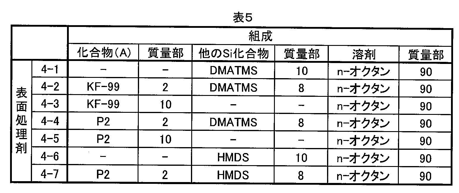
実験例4-1
表面処理剤4-1~4-7を個別に含む薬液を用いて、被処理物の表面処理を行った。表6に、表面処理の具体的な方法を示す。被処理物は、10mm×50mmの大きさのSiN膜付シリコンウェハ(SiN基板)、SiO2基板及びSi基板である。基板を、表6のNo.2-1からNo.2-14の順に、樹脂製のカップに秤取った各薬液(約5ml)に、所定の温度で所定時間浸漬させた後、20秒間窒素ガスをブローして水を除去し、速やかに接触角を測定した。尚、No.2-4におけるHF処理では、1分間の処理を行い、No.2-9における酸処理では、12%塩酸水溶液を用いた。また、SiO2基板の場合は、酸化膜が溶けてなくなってしまわないように、No.2-4における処理において、1%HF水溶液の浸漬時間を30秒間とした。更に、接触角の測定方法は、実験例1-1等と同じとした。接触角の測定結果を表7に示す。
表面処理剤4-1~4-7を個別に含む薬液を用いて、被処理物の表面処理を行った。表6に、表面処理の具体的な方法を示す。被処理物は、10mm×50mmの大きさのSiN膜付シリコンウェハ(SiN基板)、SiO2基板及びSi基板である。基板を、表6のNo.2-1からNo.2-14の順に、樹脂製のカップに秤取った各薬液(約5ml)に、所定の温度で所定時間浸漬させた後、20秒間窒素ガスをブローして水を除去し、速やかに接触角を測定した。尚、No.2-4におけるHF処理では、1分間の処理を行い、No.2-9における酸処理では、12%塩酸水溶液を用いた。また、SiO2基板の場合は、酸化膜が溶けてなくなってしまわないように、No.2-4における処理において、1%HF水溶液の浸漬時間を30秒間とした。更に、接触角の測定方法は、実験例1-1等と同じとした。接触角の測定結果を表7に示す。
実験例4-2
No.2-9における酸処理で、16%硫酸水溶液を用いた以外は、実験例4-1と同様にして、SiN基板の表面処理を行った。その結果を表7に示す。
No.2-9における酸処理で、16%硫酸水溶液を用いた以外は、実験例4-1と同様にして、SiN基板の表面処理を行った。その結果を表7に示す。
実験例4-3
No.2-9における酸処理で、20%硝酸水溶液を用いた以外は、実験例4-1と同様にして、SiN基板の表面処理を行った。その結果を表7に示す。
No.2-9における酸処理で、20%硝酸水溶液を用いた以外は、実験例4-1と同様にして、SiN基板の表面処理を行った。その結果を表7に示す。
実験例4-4
No.2-9における酸処理で、14%シュウ酸水溶液を用いた以外は、実験例4-1と同様にして、SiN基板の表面処理を行った。その結果を表7に示す。
No.2-9における酸処理で、14%シュウ酸水溶液を用いた以外は、実験例4-1と同様にして、SiN基板の表面処理を行った。その結果を表7に示す。
実験例4-5
No.2-9における酸処理を省略し、代わりに、脱イオン水に2分間浸漬した以外は、実験例4-1と同様にして、SiN基板の表面処理を行った。その結果を表7に示す。
No.2-9における酸処理を省略し、代わりに、脱イオン水に2分間浸漬した以外は、実験例4-1と同様にして、SiN基板の表面処理を行った。その結果を表7に示す。


本発明の表面処理剤を用いれば、高アスペクト比のパターンを有するようになった半導体基板等の表面を、均一に撥水化することができ、半導体の製造時の歩留まりを向上させることができる。
また、本発明の表面処理方法によれば、高アスペクト比のパターンを有するようになった半導体基板の表面を、均一に撥水化することができ、半導体の製造時の歩留まりを向上させることができる。
Claims (24)
- 下記一般式(1)で表される化合物(A)を含むことを特徴とする表面処理剤。

- 上記化合物(A)が、下記一般式(4)で表される請求項1に記載の表面処理剤。

- 上記一般式(1)におけるR1、R2、R3、R4及びR5の少なくとも1つがシアノアルキル基である請求項1に記載の表面処理剤。
- 上記化合物(A)が、下記一般式(7)で表される請求項3に記載の表面処理剤。

- 上記一般式(7)において、b/cの比が0.1~20の範囲である請求項4に記載の表面処理剤。
- 上記化合物(A)の数平均分子量が240~10,000である請求項1乃至5のいずれか一項に記載の表面処理剤。
- 更に、下記一般式(11)で表される化合物(B)を含有する請求項1乃至6のいずれか一項に記載の表面処理剤。

- 上記化合物(B)が、N,N-ジエチルアミノトリメチルシラン及びN,N-ジメチルアミノトリメチルシランのうちの少なくとも一方である請求項7に記載の表面処理剤。
- 更に、有機溶剤を含有する請求項1乃至8のいずれか一項に記載の表面処理剤。
- 被処理物の表面の撥水化に用いられる請求項1乃至9のいずれか一項に記載の表面処理剤。
- 被処理物の表面の撥水化を行う表面処理方法において、請求項1乃至9のいずれか一項に記載の表面処理剤を上記被処理物に接触させる接触工程を備えることを特徴とする表面処理方法。
- 上記被処理物が、半導体基板である請求項11に記載の表面処理方法。
- 上記被処理物が、その表面の一部に窒化ケイ素を含む請求項11又は12に記載の表面処理方法。
- 上記被処理物が、その表面の一部に酸化ケイ素を含む請求項11乃至13のいずれか一項に記載の表面処理方法。
- 上記被処理物が、その表面の一部に金属ケイ素を含む請求項11乃至14のいずれか一項に記載の表面処理方法。
- 上記接触工程の前に、酸を含む酸性液体を上記被処理物に接触させる酸接触工程を備える請求項11乃至15のいずれか一項に記載の表面処理方法。
- 上記酸が、酸解離定数(pKa)が0より小さい無機酸である請求項16に記載の表面処理方法。
- 上記被処理物が、その表面に窒化ケイ素膜と酸化ケイ素膜とを有し、上記接触工程の後、該窒化ケイ素膜の表面における水の接触角(Can)と、該酸化ケイ素膜の表面における水の接触角(Cao)との比(Can/Cao)が0.7~1.3の範囲となる請求項17に記載の表面処理方法。
- 水を含む液体と接触する工程の後、溶剤置換工程を含み、次いで、有機溶剤で希釈した表面処理剤を上記被処理物に接触させる、請求項11乃至15のいずれか一項に記載の表面処理方法。
- 半導体基板の表面の撥水化を行う表面処理方法において、酸を含む酸性液体を上記半導体基板に接触させる第1工程と、下記一般式(11)で表される化合物を含有する表面処理剤を上記半導体基板に接触させる第2工程とを、順次、備えることを特徴とする表面処理方法。

- 上記酸が、酸解離定数(pKa)が0より小さい無機酸である請求項20に記載の表面処理方法。
- 上記半導体基板が、その表面の少なくとも一部に窒化ケイ素を有する請求項20又は21に記載の半導体基板の表面処理方法。
- 上記半導体基板が、その表面の少なくとも一部に、金属ケイ素と窒化ケイ素と酸化ケイ素のうちの少なくとも2種の部分を有する請求項22に記載の半導体基板の表面処理方法。
- 上記半導体基板が、その表面に窒化ケイ素膜と酸化ケイ素膜とを有し、上記第2工程の後、該窒化ケイ素膜の表面における水の接触角(Can)と、該酸化ケイ素膜の表面における水の接触角(Cao)との比(Can/Cao)が0.7~1.3の範囲となる請求項20乃至23のいずれか一項に記載の半導体基板の表面処理方法。
Priority Applications (1)
| Application Number | Priority Date | Filing Date | Title |
|---|---|---|---|
| JP2013515097A JPWO2012157507A1 (ja) | 2011-05-17 | 2012-05-10 | 表面処理剤及び表面処理方法 |
Applications Claiming Priority (8)
| Application Number | Priority Date | Filing Date | Title |
|---|---|---|---|
| JP2011110854 | 2011-05-17 | ||
| JP2011110853 | 2011-05-17 | ||
| JP2011-110854 | 2011-05-17 | ||
| JP2011110852 | 2011-05-17 | ||
| JP2011-110852 | 2011-05-17 | ||
| JP2011-110853 | 2011-05-17 | ||
| JP2011264220 | 2011-12-02 | ||
| JP2011-264220 | 2011-12-02 |
Publications (1)
| Publication Number | Publication Date |
|---|---|
| WO2012157507A1 true WO2012157507A1 (ja) | 2012-11-22 |
Family
ID=47176837
Family Applications (1)
| Application Number | Title | Priority Date | Filing Date |
|---|---|---|---|
| PCT/JP2012/061972 Ceased WO2012157507A1 (ja) | 2011-05-17 | 2012-05-10 | 表面処理剤及び表面処理方法 |
Country Status (3)
| Country | Link |
|---|---|
| JP (1) | JPWO2012157507A1 (ja) |
| TW (1) | TW201311771A (ja) |
| WO (1) | WO2012157507A1 (ja) |
Cited By (6)
| Publication number | Priority date | Publication date | Assignee | Title |
|---|---|---|---|---|
| JP2015032735A (ja) * | 2013-08-05 | 2015-02-16 | 株式会社東芝 | 半導体基板の洗浄方法および半導体基板の洗浄装置 |
| JP2019210476A (ja) * | 2018-06-04 | 2019-12-12 | 東亞合成株式会社 | 撥水撥油膜組成物及びその利用 |
| CN111512418A (zh) * | 2017-12-22 | 2020-08-07 | 中央硝子株式会社 | 表面处理剂和表面处理体的制造方法 |
| JPWO2020196563A1 (ja) * | 2019-03-28 | 2020-10-01 | ||
| JP2022527614A (ja) * | 2019-04-09 | 2022-06-02 | ビーエーエスエフ ソシエタス・ヨーロピア | 50nm以下のライン間寸法を有するパターン化材料を処理する際のパターンの崩壊を回避するための、アンモニア活性化シロキサンを含む組成物 |
| US11981828B2 (en) | 2018-06-04 | 2024-05-14 | Toagosei Co. Ltd. | Water repellent and oil repellent film composition and use thereof |
Citations (9)
| Publication number | Priority date | Publication date | Assignee | Title |
|---|---|---|---|---|
| JPS5048296A (ja) * | 1973-08-22 | 1975-04-30 | ||
| JPS5284299A (en) * | 1976-01-01 | 1977-07-13 | Union Carbide Corp | Cyano polylkylsiloxane hydride |
| JPH06256756A (ja) * | 1993-03-08 | 1994-09-13 | Shin Etsu Chem Co Ltd | 撥水処理剤組成物 |
| JPH09310024A (ja) * | 1996-05-21 | 1997-12-02 | Toray Dow Corning Silicone Co Ltd | 硬化性オルガノポリシロキサン組成物および半導体装置 |
| JP2002241743A (ja) * | 2001-02-21 | 2002-08-28 | Shin Etsu Chem Co Ltd | 撥水砂利及びその製造方法 |
| JP2006124408A (ja) * | 2004-09-30 | 2006-05-18 | Jsr Corp | 表面疎水化用組成物、表面疎水化方法、半導体装置およびその製造方法 |
| JP2006290919A (ja) * | 2005-04-05 | 2006-10-26 | Shin Etsu Chem Co Ltd | シリコーンミスト抑制剤及びそれを含むコーティング組成物 |
| JP2010129932A (ja) * | 2008-11-28 | 2010-06-10 | Tokyo Ohka Kogyo Co Ltd | 表面処理方法及び表面処理液 |
| JP2010254927A (ja) * | 2009-04-28 | 2010-11-11 | Kaneka Corp | 光硬化可能な組成物 |
Family Cites Families (5)
| Publication number | Priority date | Publication date | Assignee | Title |
|---|---|---|---|---|
| US7857905B2 (en) * | 2007-03-05 | 2010-12-28 | Momentive Performance Materials Inc. | Flexible thermal cure silicone hardcoats |
| US7838425B2 (en) * | 2008-06-16 | 2010-11-23 | Kabushiki Kaisha Toshiba | Method of treating surface of semiconductor substrate |
| JP2010045254A (ja) * | 2008-08-15 | 2010-02-25 | Toshiba Corp | 半導体装置の製造方法 |
| US9244358B2 (en) * | 2008-10-21 | 2016-01-26 | Tokyo Ohka Kogyo Co., Ltd. | Surface treatment liquid, surface treatment method, hydrophobilization method, and hydrophobilized substrate |
| JP5882583B2 (ja) * | 2010-02-04 | 2016-03-09 | 東京応化工業株式会社 | エアギャップ形成用シリカ系被膜形成材料及びエアギャップ形成方法 |
-
2012
- 2012-05-10 WO PCT/JP2012/061972 patent/WO2012157507A1/ja not_active Ceased
- 2012-05-10 JP JP2013515097A patent/JPWO2012157507A1/ja active Pending
- 2012-05-14 TW TW101117107A patent/TW201311771A/zh unknown
Patent Citations (9)
| Publication number | Priority date | Publication date | Assignee | Title |
|---|---|---|---|---|
| JPS5048296A (ja) * | 1973-08-22 | 1975-04-30 | ||
| JPS5284299A (en) * | 1976-01-01 | 1977-07-13 | Union Carbide Corp | Cyano polylkylsiloxane hydride |
| JPH06256756A (ja) * | 1993-03-08 | 1994-09-13 | Shin Etsu Chem Co Ltd | 撥水処理剤組成物 |
| JPH09310024A (ja) * | 1996-05-21 | 1997-12-02 | Toray Dow Corning Silicone Co Ltd | 硬化性オルガノポリシロキサン組成物および半導体装置 |
| JP2002241743A (ja) * | 2001-02-21 | 2002-08-28 | Shin Etsu Chem Co Ltd | 撥水砂利及びその製造方法 |
| JP2006124408A (ja) * | 2004-09-30 | 2006-05-18 | Jsr Corp | 表面疎水化用組成物、表面疎水化方法、半導体装置およびその製造方法 |
| JP2006290919A (ja) * | 2005-04-05 | 2006-10-26 | Shin Etsu Chem Co Ltd | シリコーンミスト抑制剤及びそれを含むコーティング組成物 |
| JP2010129932A (ja) * | 2008-11-28 | 2010-06-10 | Tokyo Ohka Kogyo Co Ltd | 表面処理方法及び表面処理液 |
| JP2010254927A (ja) * | 2009-04-28 | 2010-11-11 | Kaneka Corp | 光硬化可能な組成物 |
Cited By (11)
| Publication number | Priority date | Publication date | Assignee | Title |
|---|---|---|---|---|
| JP2015032735A (ja) * | 2013-08-05 | 2015-02-16 | 株式会社東芝 | 半導体基板の洗浄方法および半導体基板の洗浄装置 |
| CN111512418A (zh) * | 2017-12-22 | 2020-08-07 | 中央硝子株式会社 | 表面处理剂和表面处理体的制造方法 |
| CN111512418B (zh) * | 2017-12-22 | 2023-08-29 | 中央硝子株式会社 | 表面处理剂和表面处理体的制造方法 |
| JP2019210476A (ja) * | 2018-06-04 | 2019-12-12 | 東亞合成株式会社 | 撥水撥油膜組成物及びその利用 |
| JP7397558B2 (ja) | 2018-06-04 | 2023-12-13 | 東亞合成株式会社 | 撥水撥油膜組成物及びその利用 |
| US11981828B2 (en) | 2018-06-04 | 2024-05-14 | Toagosei Co. Ltd. | Water repellent and oil repellent film composition and use thereof |
| JPWO2020196563A1 (ja) * | 2019-03-28 | 2020-10-01 | ||
| WO2020196563A1 (ja) * | 2019-03-28 | 2020-10-01 | 日産化学株式会社 | 膜形成用組成物 |
| JP7534720B2 (ja) | 2019-03-28 | 2024-08-15 | 日産化学株式会社 | 膜形成用組成物 |
| JP2022527614A (ja) * | 2019-04-09 | 2022-06-02 | ビーエーエスエフ ソシエタス・ヨーロピア | 50nm以下のライン間寸法を有するパターン化材料を処理する際のパターンの崩壊を回避するための、アンモニア活性化シロキサンを含む組成物 |
| JP7680366B2 (ja) | 2019-04-09 | 2025-05-20 | ビーエーエスエフ ソシエタス・ヨーロピア | 50nm以下のライン間寸法を有するパターン化材料を処理する際のパターンの崩壊を回避するための、アンモニア活性化シロキサンを含む組成物 |
Also Published As
| Publication number | Publication date |
|---|---|
| TW201311771A (zh) | 2013-03-16 |
| JPWO2012157507A1 (ja) | 2014-07-31 |
Similar Documents
| Publication | Publication Date | Title |
|---|---|---|
| JP7026782B2 (ja) | 窒化ケイ素含有基板をエッチングするための組成物および方法 | |
| US8828144B2 (en) | Process for cleaning wafers | |
| WO2012157507A1 (ja) | 表面処理剤及び表面処理方法 | |
| US9748092B2 (en) | Liquid chemical for forming protecting film | |
| JP2022524543A (ja) | 半導体装置の製造の間に窒化ケイ素を選択的に除去するためのエッチング溶液及び方法 | |
| US20170062203A1 (en) | Method of Preparing Liquid Chemical for Forming Protective Film | |
| JP7695316B2 (ja) | 半導体素子製造時に窒化ケイ素を選択的に除去するためのエッチング組成物及びエッチング方法 | |
| US12110435B2 (en) | Etching composition and method for selectively removing silicon nitride during manufacture of a semiconductor device | |
| CN112513192A (zh) | 表面处理组合物及方法 | |
| US20190341246A1 (en) | Chemical Liquid for Forming Water Repellent Protective Film | |
| JPWO2001048806A1 (ja) | 低誘電率シリカ系被膜の形成方法および低誘電率被膜付半導体基板 | |
| JP2013168583A (ja) | 表面処理剤および表面処理方法 | |
| WO2018150775A1 (ja) | 撥水性保護膜形成用薬液 | |
| US20250304856A1 (en) | Formulated Alkaline Chemistry For Polysilicon Exhume | |
| EP4662290A1 (en) | Etching compositions |
Legal Events
| Date | Code | Title | Description |
|---|---|---|---|
| 121 | Ep: the epo has been informed by wipo that ep was designated in this application |
Ref document number: 12786688 Country of ref document: EP Kind code of ref document: A1 |
|
| ENP | Entry into the national phase |
Ref document number: 2013515097 Country of ref document: JP Kind code of ref document: A |
|
| NENP | Non-entry into the national phase |
Ref country code: DE |
|
| 122 | Ep: pct application non-entry in european phase |
Ref document number: 12786688 Country of ref document: EP Kind code of ref document: A1 |