WO2012157369A1 - 熱電変換構造体およびその製造方法 - Google Patents
熱電変換構造体およびその製造方法 Download PDFInfo
- Publication number
- WO2012157369A1 WO2012157369A1 PCT/JP2012/059520 JP2012059520W WO2012157369A1 WO 2012157369 A1 WO2012157369 A1 WO 2012157369A1 JP 2012059520 W JP2012059520 W JP 2012059520W WO 2012157369 A1 WO2012157369 A1 WO 2012157369A1
- Authority
- WO
- WIPO (PCT)
- Prior art keywords
- thermoelectric conversion
- substrate
- plane
- conversion material
- srtio
- Prior art date
- Legal status (The legal status is an assumption and is not a legal conclusion. Google has not performed a legal analysis and makes no representation as to the accuracy of the status listed.)
- Ceased
Links
Images





Classifications
-
- C—CHEMISTRY; METALLURGY
- C30—CRYSTAL GROWTH
- C30B—SINGLE-CRYSTAL GROWTH; UNIDIRECTIONAL SOLIDIFICATION OF EUTECTIC MATERIAL OR UNIDIRECTIONAL DEMIXING OF EUTECTOID MATERIAL; REFINING BY ZONE-MELTING OF MATERIAL; PRODUCTION OF A HOMOGENEOUS POLYCRYSTALLINE MATERIAL WITH DEFINED STRUCTURE; SINGLE CRYSTALS OR HOMOGENEOUS POLYCRYSTALLINE MATERIAL WITH DEFINED STRUCTURE; AFTER-TREATMENT OF SINGLE CRYSTALS OR A HOMOGENEOUS POLYCRYSTALLINE MATERIAL WITH DEFINED STRUCTURE; APPARATUS THEREFOR
- C30B29/00—Single crystals or homogeneous polycrystalline material with defined structure characterised by the material or by their shape
- C30B29/10—Inorganic compounds or compositions
- C30B29/16—Oxides
- C30B29/22—Complex oxides
- C30B29/32—Titanates; Germanates; Molybdates; Tungstates
-
- H—ELECTRICITY
- H10—SEMICONDUCTOR DEVICES; ELECTRIC SOLID-STATE DEVICES NOT OTHERWISE PROVIDED FOR
- H10N—ELECTRIC SOLID-STATE DEVICES NOT OTHERWISE PROVIDED FOR
- H10N10/00—Thermoelectric devices comprising a junction of dissimilar materials, i.e. devices exhibiting Seebeck or Peltier effects
- H10N10/80—Constructional details
- H10N10/85—Thermoelectric active materials
- H10N10/851—Thermoelectric active materials comprising inorganic compositions
- H10N10/855—Thermoelectric active materials comprising inorganic compositions comprising compounds containing boron, carbon, oxygen or nitrogen
-
- C—CHEMISTRY; METALLURGY
- C04—CEMENTS; CONCRETE; ARTIFICIAL STONE; CERAMICS; REFRACTORIES
- C04B—LIME, MAGNESIA; SLAG; CEMENTS; COMPOSITIONS THEREOF, e.g. MORTARS, CONCRETE OR LIKE BUILDING MATERIALS; ARTIFICIAL STONE; CERAMICS; REFRACTORIES; TREATMENT OF NATURAL STONE
- C04B41/00—After-treatment of mortars, concrete, artificial stone or ceramics; Treatment of natural stone
- C04B41/80—After-treatment of mortars, concrete, artificial stone or ceramics; Treatment of natural stone of only ceramics
- C04B41/81—Coating or impregnation
- C04B41/85—Coating or impregnation with inorganic materials
- C04B41/87—Ceramics
-
- H—ELECTRICITY
- H10—SEMICONDUCTOR DEVICES; ELECTRIC SOLID-STATE DEVICES NOT OTHERWISE PROVIDED FOR
- H10N—ELECTRIC SOLID-STATE DEVICES NOT OTHERWISE PROVIDED FOR
- H10N10/00—Thermoelectric devices comprising a junction of dissimilar materials, i.e. devices exhibiting Seebeck or Peltier effects
- H10N10/01—Manufacture or treatment
-
- H—ELECTRICITY
- H10—SEMICONDUCTOR DEVICES; ELECTRIC SOLID-STATE DEVICES NOT OTHERWISE PROVIDED FOR
- H10N—ELECTRIC SOLID-STATE DEVICES NOT OTHERWISE PROVIDED FOR
- H10N10/00—Thermoelectric devices comprising a junction of dissimilar materials, i.e. devices exhibiting Seebeck or Peltier effects
- H10N10/10—Thermoelectric devices comprising a junction of dissimilar materials, i.e. devices exhibiting Seebeck or Peltier effects operating with only the Peltier or Seebeck effects
- H10N10/17—Thermoelectric devices comprising a junction of dissimilar materials, i.e. devices exhibiting Seebeck or Peltier effects operating with only the Peltier or Seebeck effects characterised by the structure or configuration of the cell or thermocouple forming the device
-
- H—ELECTRICITY
- H10—SEMICONDUCTOR DEVICES; ELECTRIC SOLID-STATE DEVICES NOT OTHERWISE PROVIDED FOR
- H10N—ELECTRIC SOLID-STATE DEVICES NOT OTHERWISE PROVIDED FOR
- H10N10/00—Thermoelectric devices comprising a junction of dissimilar materials, i.e. devices exhibiting Seebeck or Peltier effects
- H10N10/80—Constructional details
- H10N10/81—Structural details of the junction
Definitions
- the present invention relates to a thermoelectric conversion structure and a manufacturing method thereof. More specifically, the present invention relates to a thermoelectric conversion structure that is used for a power generation element that utilizes an environmental temperature difference and a method for manufacturing the same.
- thermoelectric power generation is only applied to niche fields such as watches using the temperature difference between the human body and the environment. The cause is that the performance of the thermoelectric conversion material used for the thermoelectric element is low.
- the unit of the figure of merit Z is K ⁇ 1
- the efficiency of the thermoelectric element using the thermoelectric conversion material is often expressed by a value obtained by multiplying it by the use temperature T (K), that is, ZT.
- the efficiency ZT of a conventional thermoelectric element using a bulk material as a thermoelectric conversion material is about 1. If a thermoelectric conversion material having an efficiency ZT exceeding 3 can be produced, it is said that a cooling system such as a compressor used in a refrigerator can be replaced.
- thermoelectric conversion material is a material having a large Seebeck coefficient S and a small resistivity and thermal conductivity.
- a typical thermoelectric conversion material currently used is Bi 2 Te 3 which is a metalloid.
- Bi 2 Te 3 materials are toxic and have a high environmental impact. Therefore, an oxide that can be a safer thermoelectric conversion material has recently attracted attention.
- an oxide thermoelectric conversion material in which La is doped at the A site in SrTiO 3 which is a perovskite oxide represented by an ABO 3 structure, is well known (Non-Patent Document 1: T. Okuda et al, Phys. Rev. B vol.63, 113104 (2001)). This material is also a degenerate semiconductor whose conductivity type is n-type.
- thermoelectric conversion material having a two-dimensional structure by using a superlattice or a one-dimensional structure using whiskers has been experimentally produced.
- an increase in Seebeck coefficient S and a decrease in resistivity ⁇ are compatible by reducing the microscopic structure of the material and manipulating the state density distribution of the conductive carrier. .
- phonon scattering increases and the thermal conductivity ⁇ decreases.
- thermoelectric conversion material having a microscopic structure with reduced dimensions an increase in the value of the figure of merit Z is achieved.
- efficiency ZT exceeds 2 by using Bi 2 Te 3 as a thermoelectric conversion material to produce a two-dimensional structure.
- Non-patent Document 2 H. Ohta et al, Nature). Mater. Vol.6, 129.
- Non-Patent Document 2 H. Ohta et al, Nature). Mater. Vol.6, 129.
- Non-Patent Document 2 shows a superlattice consisting of insulator n-type thermoelectric conversion material doped with Nb and SrTiO 3 is about 0.3 about efficiency ZT the B site of SrTiO 3
- an efficiency ZT exceeding 2 is obtained, and a Ca 3 Co 4 O 9 (p-type thermoelectric conversion material) whisker exhibits an efficiency ZT of about 1.
- thermoelectric conversion material Due to the development of thin film technology in recent years, there is no problem in producing the above superlattice (two-dimensional structure) using an oxide even if it is an oxide thermoelectric conversion material.
- an oxide when an oxide is used to produce a highly efficient thermoelectric conversion element, several problems arise.
- a quantum wire using a step of a substrate step / terrace structure as a template.
- the manufacturing conditions must be controlled so that film formation called step flow mode is realized.
- This manufacturing condition is such that the thin film growth is always performed only from the step portion, and therefore the process window is narrow and precise condition control is required.
- Another problem is that the linearity of the step of the substrate is not always ensured, and the quantum wire produced by using this as a template is not guaranteed to be linear as well.
- Patent Document 1 Japanese Patent Laid-Open No. 2004-296629.
- step bunching formed on the single crystal substrate and perpendicular to the tilt direction is used (for example, Patent Document 1, paragraph 0013).
- it is a normal step and not a bunch step that is formed on the inclined single crystal substrate surface disclosed in Patent Document 1.
- Patent Document 1 uses a buffer layer surface of a non-conductive material produced on a single crystal substrate tilted by a small angle (0.2 to 15 °) as a specific means for forming a bunch step, and It is described that a thermoelectric conversion material having a thin wire structure can be produced using the formed step bunching. However, the disclosure of Patent Document 1 does not disclose the reason why a bunched step is formed on a single crystal substrate inclined by a minute angle (0.2 to 15 °).
- the method of Patent Document 1 has the following problems. That is, (1) Since the step bunches are not formed on the substrate, a buffer layer must be formed. In addition, (2) the linearity in the extending direction of the bunched step formed on the buffer layer is not guaranteed as the linearity is not guaranteed in the normal step. For this reason, even if a bunched step is formed, the method of Patent Document 1 does not necessarily determine the thin line shape stably. Furthermore, (3) In order to form the thermoelectric conversion member made of the thermoelectric conversion material extending along the bunched step into a thin line shape, it is necessary to precisely control the manufacturing conditions as in the step flow mode.
- thermoelectric conversion material grows two-dimensionally not only from the step edge but also from the surface of the terrace, the fine line width of the thermoelectric conversion member is disturbed or the steps merge, resulting in a fine line width. May change.
- it is necessary to control the production conditions of the thermoelectric conversion material with high accuracy.
- the present invention has been made in view of any of the above problems.
- the present invention provides a thermoelectric conversion structure having a thermoelectric conversion member having a quasi-one-dimensional structure, that is, a thin wire structure, that can be manufactured easily and with high reproducibility, thereby improving the performance of a thermoelectric element that employs the thermoelectric conversion structure. It contributes to.
- the inventor of the present application examines the above problems, and step bunching in which the step formed on the buffer layer on the single crystal substrate inclined by a small angle (0.2 to 15 °) is high does not provide an essential solution. I thought. In order to easily produce a thin wire structure with good reproducibility using an oxide thermoelectric conversion material, the inventor is effective to form a concavo-convex structure defined by crystal axes and crystal planes on the surface of the substrate. In order to achieve this, it has been found that it is effective to use the (210) plane orientation SrTiO 3 as a substrate.
- the concavo-convex structure has a (210) substrate surface, and includes a terrace portion formed by the (100) surface and a step portion extending in an in-plane [001] axis of the substrate surface.
- a thermoelectric conversion structure comprising a substrate of SrTiO 3 having a surface and a thermoelectric conversion material disposed on at least a part of the surface of the concavo-convex structure.
- a concavo-convex structure is formed on the substrate surface, which is the (210) plane of SrTiO 3 , by the terrace portion by the (100) plane and the step portion extending in the in-plane [001] axis.
- the concavo-convex structure has a height difference as much as 12 unit cells, for example.
- the minute surface forming the concavo-convex structure is defined by a terrace portion made of (100) plane and a step portion extending along the [001] axis, that is, a crystal axis and a crystal plane. And this uneven structure is utilized as a template for a thermoelectric conversion member.
- thermoelectric conversion member is formed on at least a part of the surface of the concavo-convex structure. At that time, it is not necessary to form a buffer layer or the like. Moreover, in the concavo-convex structure, linearity of the shape of the thermoelectric conversion material forming the thermoelectric conversion member is ensured. This is because the step portion is formed along the [001] axis.
- the difference in the electric conduction characteristic also affects the Seebeck coefficient.
- the influence of anisotropy appearing in the electric conduction characteristics can be sufficiently detected not only at a low temperature but also in a temperature range of room temperature (for example, about 300K).
- a quasi-one-dimensional structure an arbitrary structure that causes a difference in macroscopic electric conduction characteristics by further reducing the two-dimensional electron system is referred to as a quasi-one-dimensional structure.
- the substrate of (210) plane orientation means a substrate whose substrate surface is the (210) plane in terms of the plane index of the crystal lattice of the substrate.
- the substrate surface here is a plane on which the surface of interest of the substrate generally extends. For example, if some microscopic structure is formed on the surface of interest of the substrate, the surface that defines the surface of the entire substrate, not the orientation of the individual microsurfaces that define the microscopic structure Becomes the substrate surface. Further, a deviation in orientation due to an error that remains in production, such as a miscut angle, is allowed for determination of the substrate surface.
- a (210) -oriented substrate will be described by way of a specific example.
- a (210) -oriented substrate is an orientation of a crystal lattice (hereinafter referred to as “orientation”) such that a Miller index specifying a substrate surface is a (210) plane. It is a substrate that has been determined.
- the (100) plane of the crystal lattice in the substrate of this embodiment is greatly inclined by about 26.6 ° from the (210) plane which is the substrate plane. That is, when the surface of the substrate is traced in the [1-20] axial direction, the terrace portion by the (100) plane is divided into a large number of fragments having a short length, and there is a large difference in level difference between the terrace portions. Is formed as a step portion or the like. For this reason, even if two-dimensional growth is performed on the (100) plane, the grown thermoelectric conversion material is interrupted or the film is bent at the level difference.
- thermoelectric conversion material grown on the concavo-convex structure of the substrate substantially forms a thermoelectric conversion member having a one-dimensional structure even if it is formed on the (100) plane under two-dimensional growth conditions. Details of this mechanism will be described later in Examples. Therefore, in this embodiment, a one-dimensional structure can be produced with good reproducibility by the same simplicity as that for producing a two-dimensional structure. Thereby, in this aspect, it becomes possible to increase the figure of merit Z of the oxide thermoelectric conversion material.
- SrTiO 3 is formed with a thickness of 5 unit cells or more so as to cover the thermoelectric conversion material, and has an additional concavo-convex structure formed corresponding to the concavo-convex structure on the surface.
- a thermoelectric conversion structure according to the above aspect further comprising: an additional thermoelectric conversion material disposed on the surface of at least a part of the additional uneven structure on the surface of the coating layer.
- the coating layer has a thickness of 10 unit cells or more.
- thermoelectric conversion structure according to the above aspect, wherein the thickness of the thermoelectric conversion material is 3 unit cells or less when measured in the [100] axial direction of the substrate.
- thermoelectric conversion structure having a higher figure of merit Z, in which the effect of lowering the dimension is more strongly expressed.
- thermoelectric conversion material La, Pr, SrTiO 3 at least one of Nd doped at the A site, or in any of the SrTiO 3 doped with Nb at the B site
- thermoelectric conversion structure according to one aspect is provided.
- thermoelectric conversion member since the lattice constant of the thermoelectric conversion material is close to that of SrTiO 3 which is the material of the substrate, the thermoelectric conversion member having a fine wire structure with good crystallinity and SrTiO 3 that insulates it are laminated in multiple layers. It becomes possible. Thereby, it is possible to increase the number of thermoelectric conversion member lines per unit volume, that is, the degree of integration while maintaining a high figure of merit Z.
- thermoelectric conversion structure in one aspect of the present invention, a method for manufacturing a thermoelectric conversion structure is provided. That is, by annealing a SrTiO 3 substrate having a (210) plane substrate surface in the atmosphere, a terrace portion by the (100) plane and a step portion extending in the in-plane [001] axis of the substrate plane are included.
- a method for producing a thermoelectric conversion structure including a step of forming a concavo-convex structure and a step of disposing a thermoelectric conversion material on at least a part of the surface of the concavo-convex structure.
- an additional concavo-convex structure formed corresponding to the concavo-convex structure is formed on the surface of the coating layer by forming a SrTiO 3 coating layer so as to cover the thermoelectric conversion material.
- a method for manufacturing a thermoelectric conversion structure further comprising: a step of forming an additional thermoelectric conversion material on at least a part of the surface of the additional uneven structure on the surface of the covering layer. .
- the A site is a perovskite crystal lattice expressed as ABO 3, and is considered to be a cube having each oxygen forming an oxygen octahedron at the face center position, more generally a parallelepiped, It is a grid point located at the vertex of a cube or the like.
- thermoelectric conversion structure having a thin wire structure or a quasi-one-dimensional structure is provided.
- thermoelectric conversion structure which shows the high figure of merit Z, and the thermoelectric conversion element using the same are realized.
- thermoelectric conversion element in an embodiment with this invention.
- SrTiO 3 cubic perovskite structure which is a substrate of the embodiment of the present invention, is a schematic side view showing a crystal lattice of (210) plane orientation.
- 2A is a side view of the in-plane [1-20] axis
- FIG. 2B is a side view of the in-plane [001] axis.
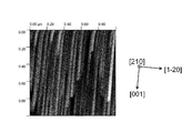
- It is an AFM image of the (210) plane orientation substrate surface of the SrTiO 3 substrate after annealing in the atmosphere at 1180 ° C. for 12 hours in an embodiment of the present invention.
- a quasi-one-dimensional structure is formed on a concavo-convex structure including a terrace portion of the (100) plane of the surface of the SrTiO 3 (210) plane orientation substrate and a step portion parallel to the [001] axis direction.
- thermoelectric conversion element having thermoelectric conversion member consisting of La-doped SrTiO 3 formed (thermoelectric conversion material) to.
- thermoelectric conversion structure is formed on a concavo-convex structure including a terrace portion of the (100) plane of the surface of the SrTiO 3 (210) plane orientation substrate and a step portion parallel to the [001] axis direction.
- thermoelectric conversion member consisting of La-doped SrTiO 3, which are integrated (thermoelectric conversion material) to. It is a flowchart which shows the preparation procedures of the thermoelectric conversion structure in one embodiment of this invention.
- thermoelectric conversion structure according to the present invention.
- common parts or elements are denoted by common reference numerals throughout the drawings.
- each element of each embodiment is not necessarily shown in a scale ratio.
- thermoelectric conversion structure according to the present embodiment will be described with reference to the drawings.
- an uneven structure defined by the [001] axis and the (100) plane is formed on the surface of the (210) -oriented SrTiO 3 substrate, and the La-doped SrTiO 3 produced on the surface is used as the thermoelectric conversion material.
- the thermoelectric conversion structure by the thin-wire structure thermoelectric conversion member produced is demonstrated.
- FIG. 1 is a schematic cross-sectional view showing the configuration of the thermoelectric conversion structure 100 of the present embodiment.
- the thermoelectric conversion structure 100 includes a substrate 10 and a thermoelectric conversion member 20 formed on the surface of the substrate 10.
- the substrate 10 is a substrate made of SrTiO 3 having a surface having a concavo-convex structure when viewed finely.
- a thermoelectric conversion member 20 is formed in contact with the surface of the SrTiO 3 substrate.
- the vertical direction of the paper is drawn so as to be perpendicular to the substrate surface and the horizontal direction is parallel to the substrate surface.
- thermoelectric conversion member 20 is made of a La-doped SrTiO 3 thermoelectric conversion material and has almost the same lattice constant as that of the SrTiO 3 of the substrate 10 and is epitaxially grown on the surface of the substrate 10.
- this cubic perovskite structure is a crystal structure of both the substrate 10 that is the SrTiO 3 substrate and the La-doped SrTiO 3 thermoelectric conversion material 22 that is the thermoelectric conversion member 20.
- the perovskite structure is expressed as ABO 3 , where A is the apex, B is the body center, and O (oxygen) is the face center.
- the apex site is called the A site, and the atoms occupying the A site are called A atoms.
- the vertical direction of the paper surface is the direction perpendicular to the substrate surface (hereinafter referred to as the “perpendicular direction”)
- FIG. 2A shows the in-plane [001] axis
- FIG. 2B shows the in-plane orthogonal [1-20]. It is sectional drawing seen from the axis
- ⁇ arctan (1/2) Equation 2 That is, ⁇ is about 26.6 degrees, and atomic planes are alternately stacked with AO—BO 2 —AO.
- the interval in the perpendicular direction is about 0.5238 nm for 3d (210).
- the length in the direction perpendicular to the plane in consideration of the in-plane atomic position periodicity is about 0.873 nm for 5d (210).
- FIG. 3 shows an AFM image of the surface of the substrate 10 used in the thermoelectric conversion structure 100 of the present embodiment.
- FIG. 4 is a schematic cross-sectional view showing an enlarged structure near the surface of the substrate 10.
- the substrate 10 has a (100) plane terrace portion formed in a top terrace portion 12 and a bottom terrace portion 14 (hereinafter, “top” and “bottom” are not explicitly described).
- the substrate 10 is provided with a concavo-convex structure including a step portion 16 extending in the in-plane [001] axis of the substrate surface.
- thermoelectric conversion structure 100 the (100) plane terrace portions 12 and 14 of the single crystal plane and the step portion 16 extending parallel to the in-plane [001] axial direction are not formed on the substrate 10 at the purchase stage. That is, the surface of the single crystal of the substrate 10 at the purchase stage is flat at the nm level, and no regular structure is observed.
- the SrTiO 3 (210) substrate is annealed in the atmosphere at 1180 ° C. for 12 hours, an uneven structure as shown in FIGS. 3 and 4 is observed.
- thin terrace portions 12 and 14 having a width W of about 20 nm extending in the [001] axial direction with a length of 1 ⁇ m or more are formed on the surface of the substrate 10.
- the height difference L when the surface is traced in the axial direction is about 6 nm.
- the formed height difference L is approximately 12 in terms of unit cell of SrTiO 3 which is the material of the substrate 10.
- SrTiO 3 which is the material of the substrate 10.
- the unit 16 is connected to the step unit 18 in the reverse direction. Of these step units, the step unit 16 is constituted by a [010] plane. On the other hand, it is not certain what kind of relation the surface of the reverse step portion 18 has with the crystal axis.
- the concavo-convex structure that causes a large height difference L is formed by combining the terrace portions 12 and 14 and the step portions 16 and 18, and the step portion 18 is opposite to the step portion 16. It seems to have a tilt of direction.
- the terrace portions 12 and 14 and the step portions 16 and 18 both extend in the [001] axial direction and are arranged so as to be aligned in the [1-20] axial direction.
- the step portion 16 has a clear relationship with the crystal lattice of (010) plane, so the step portion 16 is higher in the [001] axial direction than the step portion 18. Extends with accuracy.
- thermoelectric conversion member 20 formed in the board
- substrate 10 is shown as sectional drawing. That is, the thermoelectric conversion structure 100 has a concavo-convex structure including the terrace portions 12 and 14 on the (100) plane of the SrTiO 3 (210) plane orientation substrate surface and the step portions 16 and 18 parallel to the [001] axis direction.
- the thermoelectric conversion member 20 including La-doped SrTiO 3 (thermoelectric conversion material 22) formed to have a quasi-one-dimensional structure is provided.
- the thermoelectric conversion member 20 typically has a structure in which a number of elongated strips of the thermoelectric conversion material 22 are arranged.
- thermoelectric conversion material 22 is formed on the surface of the concavo-convex structure on which the terrace portions 12 and 14 formed of the (100) plane of the substrate surface of the SrTiO 3 (210) plane orientation and the step portion 16 of the (100) plane are formed. Is formed.
- the thermoelectric conversion material 22 covers at least a part of the surface of the concavo-convex structure.
- FIG. 5 is a cross-sectional view in the case where each of the elongated strips of the thermoelectric conversion material 22 of the thermoelectric conversion member 20 extending in the [001] axis direction is cut by a plane perpendicular to the [001] axis.
- the thermoelectric conversion material 22 that forms the thermoelectric conversion member 20 is subjected to thermoelectric conversion by passing a current in the longitudinal direction, that is, in a direction perpendicular to the paper surface in FIGS. 4 and 5. And since it is formed on the uneven structure on the surface of the substrate 10 described above, the thermoelectric conversion material 22 has a pseudo one-dimensional structure (pseudo one-dimensional structure).
- thermoelectric conversion structure 100 Due to this quasi-one-dimensional structure, a good value of the efficiency ZT of the thermoelectric conversion structure 100 can be obtained. That is, each of the elongated strips of the thermoelectric conversion material 22 becomes an electron-rich degenerate semiconductor, so that a quasi-one-dimensional structure is also introduced into the spatial distribution of electrons. This highly anisotropic electronic structure increases the efficiency ZT of the thermoelectric conversion structure 100.
- thermoelectric conversion member 20 of the thermoelectric conversion structure 100 may not be separated into elongated strips like the thermoelectric conversion material 22 as shown in FIG.
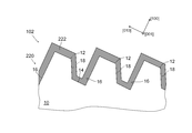
- FIG. 6 shows a thermoelectric conversion structure 102 having a thermoelectric conversion member 220 having another structure having a quasi-one-dimensional structure formed so as to be in contact with the surface of the concavo-convex structure similar to FIG.
- the thermoelectric conversion member 220 includes a thermoelectric conversion material 222 formed so as to cover the terrace portions 12 and 14 and the step portions 16 and 18 having an uneven structure.
- thermoelectric conversion material 222 Since such a thermoelectric conversion material 222 is a film formed along the concavo-convex structure, the electron conduction characteristics are affected by the influence of the [001] axis (perpendicular to the paper surface) and the [1-20] axis. (The left-right direction of the page) is greatly different. Such an effect is prominent when the thickness of the thermoelectric conversion material 222 is as thin as about 3 unit cells, for example, when the thickness is defined in the [100] axis direction in the (100) plane terrace portion 12. .
- thermoelectric conversion structure of this embodiment the gap where the thermoelectric conversion material in contact with the surface of the concavo-convex structure is discontinuous on the surface of the concavo-convex structure as in the thermoelectric conversion material 22 shown in FIG. It is not always necessary to form.
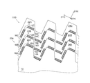
- thermoelectric conversion structure 110 which is a modification of this embodiment is shown with schematic sectional drawing.
- the thermoelectric conversion structure 110 of the present embodiment as with the thermoelectric conversion member 20a, the terrace portions 12A and 14A and the step portions 16A and 18A formed on the substrate 10 are integrated.
- the converted thermoelectric conversion material 22 (22A to 22C) can be employed.
- the thermoelectric conversion material 22A made of La-doped SrTiO 3 includes irregularities including terrace portions 12A and 14A and a step portion 16A. Formed on the surface of at least a portion of the structure. Thereafter, a coating layer 24A of SrTiO 3 is formed so as to cover the thermoelectric conversion material 22A.
- the typical coating layer 24A is formed with a thickness of 5 unit cells or more.
- An additional concavo-convex structure corresponding to the concavo-convex structure of the substrate 10 is formed by growing the coating layer 24A so as to form a continuous crystal on the thermoelectric conversion material 22A. That is, the SrTiO 3 coating layer 24A is epitaxially grown on the La-doped SrTiO 3 thermoelectric conversion material 22A. In the initial stage of forming the covering layer 24A, the gap between the thermoelectric conversion materials 22A is filled with the covering layer 24A.
- the structure similar to the concavo-convex structure in which the terrace portions 12A and 14A and the step portions 16A and 18A are formed is homogeneous.
- a concavo-convex structure is formed as if it were formed of a material.
- the coating layer 24A covers the thermoelectric conversion material 22A, and an additional uneven structure is obtained in which only the material of the coating layer 24A is located on the surface.
- This additional uneven structure includes terrace portions 12B and 14B and step portions 16B and 18B.
- the structure of the thermoelectric conversion materials 22A to 22C that are La-doped SrTiO 3 is substantially a quasi-one-dimensional structure, particularly when the film thickness is equal to or less than 3 unit cells. This is because the (100) plane is inclined by about 26.6 ° from the (210) plane, and the shape when the (100) plane terrace sections 12 and 14 are traced is not linear. This is because La-doped SrTiO 3 corresponding to a film thickness of 3 unit cells or less formed on the surface of 14, the valley bottom of the step, and the side surface is cut. And if the thermoelectric conversion member 20a of such an integrated structure is employ
- thermoelectric conversion structure 110 when thermoelectric conversion is performed by the thermoelectric conversion materials 22A to 22C forming the thermoelectric conversion member 20a, the longitudinal direction of the thermoelectric conversion materials 22A to 22C, that is, the direction perpendicular to the paper surface in FIG. A current is passed through.
- FIG. 8 is a flowchart showing the manufacturing procedure.
- the manufacture of the thermoelectric conversion structure 100 is started by producing the substrate 10 on which the concavo-convex structure is formed by annealing the substrate in the atmosphere as described above (S102).
- thermoelectric conversion material is formed on the concavo-convex structure by laser ablation (S104). More specifically, La-doped SrTiO 3 is grown on the surface of the concavo-convex structure as the thermoelectric conversion material of the thermoelectric conversion material 22 to be formed.
- a target obtained by forming a polycrystalline material produced by a solid phase reaction method into a cylindrical shape of ⁇ 20 mm ⁇ 5 mm so that the La doping amount is 10% is used.
- the detailed procedure is as follows. First, the substrate 10 which is a SrTiO 3 (210) substrate is mounted in a vacuum chamber and evacuated to 3 ⁇ 10 ⁇ 9 Torr (4 ⁇ 10 ⁇ 7 Pa) or less.
- the substrate 10 on which the concavo-convex structure is already formed is heated to an ultimate temperature of 750 ° C. Since the temperature of the substrate 10 during the film formation is lower than 1180 ° C. when the substrate annealing temperature is formed, the concavo-convex structure formed on the surface of the substrate 10 is the same as that in the laser ablation method. Unaffected by substrate heating.
- the target is irradiated with 135 pulses of a KrF excimer laser having a wavelength of 248 nm through the laser beam introduction port of the chamber to grow La-doped SrTiO 3 corresponding to a film thickness of 3 unit cells on the concavo-convex structure.
- a KrF excimer laser having a wavelength of 248 nm
- the target is irradiated with 135 pulses of a KrF excimer laser having a wavelength of 248 nm through the laser beam introduction port of the chamber to grow La-doped SrTiO 3 corresponding to a film thickness of 3 unit cells on the concavo-convex structure.
- thermoelectric conversion material 22 the substrate 10 is a SrTiO 3, conditions such as the epitaxial growth of the thermoelectric conversion material 22 having substantially the same lattice constant as SrTiO 3 has been selected. For this reason, in order to confirm the crystallinity in the growth of the thermoelectric conversion material 22, it is effective to perform in-situ observation by RHEED (reflection high-energy electron diffraction). That is, the substrate 10 which is the (210) substrate is anisotropic, and diffraction with respect to the (1-20) plane is obtained when an electron beam is incident parallel to the in-plane [001] axis. When such observation is actually performed, for example, diffraction patterns from the (100) plane and the (010) plane can be seen.
- RHEED reflection high-energy electron diffraction
- the diffraction pattern of the thin film of the thermoelectric conversion material 22 maintains the configuration of the surface including the terrace portions 12 and 14 by the (100) plane and the step portion 16 by the (010) plane, similarly to the uneven structure on the surface of the substrate 10. That is, it can be confirmed that the concavo-convex structure of the substrate 10 is used as a template.
- information on the in-plane (001) plane can also be obtained by entering parallel to the in-plane [1-20] axis. When an electron beam is incident in parallel to the [1-20] axis, a RHEED pattern consisting of streaks is observed, and no step is formed in the [001] axis direction. Is confirmed to be obtained.
- thermoelectric conversion member 20 formed thereon, the thermoelectric conversion material formed on the surface of the concavo-convex structure of the substrate 10.
- No. 22 is defined by the thickness in the direction perpendicular to the surface. Further, the thermoelectric conversion materials 22 adjacent to each other in the [1-20] direction are separated from each other by the height difference created by the step portions 16 and 18 having the concavo-convex structure. In this way, a quasi-one-dimensional structure is realized.
- thermoelectric conversion structure 100 can be manufactured by the above steps (S102, S104, S108).
- the process (S106) of forming a coating layer is implemented following process S104.
- the coating layer 24A corresponding to 10 unit cells is similarly formed using the SrTiO 3 target in the same vacuum chamber.
- the covering layer 24A forms a crystal lattice epitaxially on the concavo-convex structure of the substrate 10 together with the thermoelectric conversion material 22A.
- a thermoelectric conversion structure 110 having a sectional view as shown in FIG. 7 is formed.
- thermoelectric conversion structure 110 An example sample having the same structure as the thermoelectric conversion structure 110 described above was produced, and a figure of merit Z of the thermoelectric conversion structure of the example sample was obtained. Specifically, Al electrodes are formed at both ends in the [001] axial direction of the example sample, and the Seebeck coefficient S, resistivity ⁇ , and thermal conductivity ⁇ indicated by the thermoelectric conversion member 20a are set to room temperature (300K) through the Al electrodes.
- the reason why the most excellent efficiency can be obtained when Pr is doped is considered to be that the distortion of the oxygen octahedron made of TiO 6 increases because the ion radius of Pr is smaller than that of La. That is, it is considered that the decrease in resistivity and the decrease in thermal conductivity due to the improvement in mobility caused by strain contribute to the improvement in efficiency ZT.
- thermoelectric conversion material formed on the surface of the concavo-convex structure defined by the step portion extending on the [001] axis of the (210) plane orientation SrTiO 3 substrate surface and the terrace portion of the (100) plane here In La-doped SrTiO 3
- a quasi-one-dimensional structure is formed.
- thermoelectric conversion material having a quasi-one-dimensional structure by forming an SrTiO 3 insulating layer on the thermoelectric conversion material and repeating this sequence.
- the uneven structure with a large elevation difference can be easily formed with high reproducibility simply by annealing the (210) plane orientation SrTiO 3 substrate in the atmosphere.
- thermoelectric conversion material capable of improving performance can be obtained.
- the composition of the thermoelectric conversion material illustrated by this embodiment, a film thickness, a formation method, etc. are not limited to the said embodiment.
- the materials, compositions, film thicknesses, formation methods, and the like of the thin film and the substrate exemplified in this embodiment are not limited to the above embodiments.
- the names of axes and planes for the perovskite crystal described for explanation can be expressed based on another equivalent expression as known to those skilled in the art.
- the crystal axis extending to the substrate surface is expressed as the [001] axis
- the setting of the [100] axis and the [010] axis is also arbitrary.
- a surface expressed as the (m10) plane by taking a right-handed axis is a (1m0) plane according to another way of taking the right-handed system and is equivalent to each other. Care must be taken that the face becomes a different expression.
- the present invention can be used as a thermoelectric conversion structure for a thermoelectric conversion element that generates electricity using a temperature difference in the environment.
- Thermoelectric conversion structure 10 Substrate 12, 12A, 12B, 12C (100) plane (top terrace) 14, 14A, 14B, 14C (100) plane (bottom terrace) 16, 16A, 16B, 16C Step part ((010) plane) 18, 18A, 18B, 18C Step part (reverse direction) 20, 20a, 220 Thermoelectric conversion member 22, 222, 22A, 22B, 22C La-doped SrTiO 3 (thermoelectric conversion material with quasi-one-dimensional structure) 24, 24A, 24B, 24C Coating layer
Landscapes
- Chemical & Material Sciences (AREA)
- Engineering & Computer Science (AREA)
- Inorganic Chemistry (AREA)
- Materials Engineering (AREA)
- Organic Chemistry (AREA)
- Crystallography & Structural Chemistry (AREA)
- Metallurgy (AREA)
- Manufacturing & Machinery (AREA)
- Ceramic Engineering (AREA)
- Structural Engineering (AREA)
- Crystals, And After-Treatments Of Crystals (AREA)
- Inorganic Compounds Of Heavy Metals (AREA)
Abstract
Description
Z=S2/(ρ・κ) 式1
によって表わされる。ただし、Sはゼーベック係数(μV/K)、ρは抵抗率(Ωcm)、κは熱伝導率(W/(m・K))である。なお、性能指数Zの単位はK-1となり、熱電変換材料を用いる熱電素子の効率としては、それに使用温度T(K)を乗じた値すなわちZTを用いて表わされることが多い。ちなみに、熱電変換材料としてバルク材料を用いる従来の熱電素子の効率ZTは1程度である。この効率ZTが3を越す熱電変換材料を作製することができれば、例えば冷蔵庫に使用されるコンプレッサー等の冷却システムを置き換えることも可能になると言われている。
以下、本実施形態の熱電変換構造体の実施形態を図面に基づいて説明する。ここでは(210)面方位のSrTiO3の基板の表面において、[001]軸と(100)面により規定される凹凸構造を形成し、その表面上に作製したLaドープSrTiO3を熱電変換材料として作製される細線構造の熱電変換部材による熱電変換構造体について説明する。特に本実施形態では、その凹凸構造を利用して作製された擬一次元構造を有する熱電変換部材がいかに再現性よく簡単に形成されるかが説明される。
[1-1 全体構造]
まず始めに、本実施形態の熱電変換構造体の構成について説明する。図1は、本実施形態の熱電変換構造体100の構成を示す概略断面図である。熱電変換構造体100は、基板10と、その基板10の表面に形成された熱電変換部材20とによって構成される。このうち、基板10は、後述するように、微細に見ると凹凸構造となっている表面を備えているSrTiO3からなる基板である。そのSrTiO3基板の表面に接するように熱電変換部材20が形成されている。なお、図1においては、紙面の上下方向が基板面に垂直になり、左右方向が基板面に平行になるように描いている。熱電変換部材20は、LaドープSrTiO3の熱電変換材料から構成されており、基板10のSrTiO3とほとんど同じ格子定数であり基板10の表面に対してエピタキシャル成長している。
次に、図2を参照して、立方晶ペロフスカイト構造における(210)面方位を説明する。この立方晶ペロフスカイト構造は、本実施形態においては、SrTiO3基板である基板10と、熱電変換部材20であるLaドープSrTiO3の熱電変換材料22との双方の結晶構造である。ペロフスカイト構造はABO3と表記され、Aは頂点、Bは体心、O(酸素)は面心の各位置を占める。本実施形態の説明において、頂点のサイトをAサイトとよび、そこを占める原子をA原子と呼ぶ。紙面縦方向を基板面に垂直な方向(以降「面直方向」と呼ぶ)とし、図2(a)は面内[001]軸、図2(b)はそれと直交する面内[1-20]軸からみた断面図である。この立方晶ペロフスカイト構造において(210)面から測った(100)面の角度は式2で表わされる。
θ=arctan(1/2) 式2
すなわちθは約26.6度であり、面直方向にAO-BO2-AO・・・と交互に原子面が積み重なっている。SrTiO3(210)の基板10では、面直方向(210)面の面間隔は
d(210)=a・sinθ 式3
から求められ、約0.1746nmとなる。なお、aはSrTiO3の格子定数(=0.3905nm)である。また、立方晶のユニットセルが(100)面方位から約26.6度傾いたという見方をすると、面直方向の間隔は3d(210)は約0.5238nmである。なお、面内原子位置周期性まで考慮した面直方向の長さは5d(210)は約0.873nmとなる。これらの格子定数は、熱電変換部材20をなす熱電変換材料22においてもほとんど同一である。
次に基板10であるSrTiO3(210)面方位基板表面の構造について説明する。図3は、本実施形態の熱電変換構造体100に用いる基板10の表面のAFM像を示す。また、図4は、基板10の表面付近の構造を拡大して示す概略断面図である。図4に示すように、基板10には、(100)面によるテラス部が、頂部テラス部12と底部テラス部14とに形成されている(以下「頂部」「底部」の記載は明示しない)。また、基板10には、基板面の面内[001]軸に延びるステップ部16を含む凹凸構造が形成される。
図5に、基板10に形成される熱電変換部材20の構成を断面図として示している。すなわち、熱電変換構造体100は、SrTiO3(210)面方位基板表面の(100)面のテラス部12、14と[001]軸方向に平行なステップ部16、18とからなる凹凸構造上に擬一次元構造になるように形成されたLaドープSrTiO3(熱電変換材料22)を含む熱電変換部材20を有している。熱電変換部材20は、典型的には、熱電変換材料22の細長のストリップを多数並べた構造となっている。そして、熱電変換材料22は、SrTiO3(210)面方位の基板表面の(100)面からなるテラス部12、14と(100)面のステップ部16とが形成されている凹凸構造の表面に形成されている。熱電変換材料22は、その凹凸構造の表面の少なくとも一部を覆っている。
図7に、本実施形態の変形例である熱電変換構造体110を概略断面図により示す。図7に示すように、本実施形態の熱電変換構造体110においては、熱電変換部材20aのように、基板10に形成されているテラス部12A、14A、ステップ部16A、18Aを利用して集積化された熱電変換材料22(22A~22C)を採用することができる。この熱電変換構造体110を作製するためには、図5に示した熱電変換構造体100と同様に、LaドープSrTiO3による熱電変換材料22Aが、テラス部12A、14Aとステップ部16Aを含む凹凸構造の少なくとも一部の表面に形成される。その後にその熱電変換材料22Aを覆うようにSrTiO3の被覆層24Aが形成される。
次に、本実施形態の熱電変換構造体100および熱電変換構造体110の製造方法について説明する。図8は、その作製手順を示すフローチャートである。熱電変換構造体100の製造は、まず、上述したように大気中において基板をアニール処理することによって、凹凸構造が形成されている基板10を作成することから開始する(S102)。
以下に実施例を挙げて本発明をさらに具体的に説明する。以下の実施例に示す材料、使用量、割合、処理内容、処理手順、要素または部材の向きや具体的配置等は本発明の趣旨を逸脱しない限り適宜変更することかできる。したがって、本発明の範囲は以下の具体例に限定されるものではない。上述した熱電変換構造体110と同一の構造の実施例サンプルを作製し、実施例サンプルの熱電変換構造体の性能指数Zを求めた。具体的には、実施例サンプルの[001]軸方向の両端にAl電極を形成し、そのAl電極を通じて熱電変換部材20aの示すゼーベック係数S、抵抗率ρ、および熱伝導率κを室温(300K)で測定する。するとNbドープしたSrTiO3とSrTiO3からなる超格子で報告されている効率ZTが約0.3(超格子界面だけに限ればZT>2)よりもはるかに優れた効率ZTである約4.6の効率ZTが測定される(T=300K)。このような特性が得られた理由として、本願の発明者は、本発明により熱電変換材料であるLaドープしたSrTiO3の電子状態が実質的に擬一次元化されたためであると考えている。また、上記と同様にAサイトにPr及びNdを10%ドープした試料の効率ZTについても、5.8、4.3とそれぞれ優れた値が得られる(T=300K)。Prをドープした場合に最も優れた効率が得られる理由としては、Laと比べてPrのイオン半径が小さいためにTiO6からなる酸素八面体の歪が大きくなることが考えられる。すなわち、歪によって生じる移動度の向上による抵抗率の減少と熱伝導率の減少とが効率ZTの向上に寄与するものと考えられる。一方、BサイトにNbを10%ドープした試料では、2.9の効率ZT、つまり、Aサイトにドープした場合よりも小さいながらも優れた効率が得られることを付記しておく(T=300K)。
10 基板
12、12A、12B、12C (100)面(頂部テラス部)
14、14A、14B、14C (100)面(底部テラス部)
16、16A、16B、16C ステップ部((010)面)
18、18A、18B、18C ステップ部(逆向き)
20、20a、220 熱電変換部材
22、222、22A、22B、22C LaドープSrTiO3(擬一次元構造の熱電変換材料)
24、24A、24B、24C 被覆層
Claims (6)
- (210)面の基板面を有しており、(100)面によるテラス部と該基板面の面内[001]軸に延びるステップ部とを含む凹凸構造を有するSrTiO3の基板と、
該凹凸構造の少なくとも一部の表面に配置されている熱電変換材料と
を備えている
熱電変換構造体。 - 前記熱電変換材料を覆うように5ユニットセル以上の厚みで形成されており、前記凹凸構造に対応して形成された追加の凹凸構造を表面に有するSrTiO3の被覆層と、
該被覆層の表面の該追加の凹凸構造の少なくとも一部の表面に配置されている追加の熱電変換材料と
をさらに備えている
請求項1に記載の熱電変換構造体。 - 前記熱電変換材料の厚みが、前記基板の[100]軸方向に測ったときに3ユニットセル以下である
請求項2に記載の熱電変換構造体。 - 前記熱電変換材料が、La、Pr、Ndの少なくともいずれかをAサイトにドープしたSrTiO3、または、NbをBサイトにドープしたSrTiO3のいずれかである
請求項3に記載の熱電変換構造体。 - (210)面の基板面を有するSrTiO3の基板を大気中にてアニールすることにより、(100)面によるテラス部と該基板面の面内[001]軸に延びるステップ部とを含む凹凸構造を形成する工程と、
該凹凸構造の少なくとも一部の表面に熱電変換材料を配置する工程と
を含む
熱電変換構造体の製造方法。 - SrTiO3の被覆層を前記熱電変換材料を覆うように形成することにより、前記凹凸構造に対応して形成された追加の凹凸構造を該被覆層の表面に形成する工程と、
該被覆層の表面の該追加の凹凸構造の少なくとも一部の表面に、追加の熱電変換材料を配置する工程と
をさらに含む
請求項5に記載の熱電変換構造体の製造方法。
Priority Applications (3)
| Application Number | Priority Date | Filing Date | Title |
|---|---|---|---|
| KR1020137009174A KR20140021510A (ko) | 2011-05-19 | 2012-04-06 | 열전 변환 구조체 및 그 제조 방법 |
| JP2013515046A JP5472534B2 (ja) | 2011-05-19 | 2012-04-06 | 熱電変換構造体およびその製造方法 |
| US13/878,966 US8872016B2 (en) | 2011-05-19 | 2012-04-06 | Thermoelectric conversion structure and method of manufacturing same |
Applications Claiming Priority (2)
| Application Number | Priority Date | Filing Date | Title |
|---|---|---|---|
| JP2011-111943 | 2011-05-19 | ||
| JP2011111943 | 2011-05-19 |
Publications (1)
| Publication Number | Publication Date |
|---|---|
| WO2012157369A1 true WO2012157369A1 (ja) | 2012-11-22 |
Family
ID=47176710
Family Applications (1)
| Application Number | Title | Priority Date | Filing Date |
|---|---|---|---|
| PCT/JP2012/059520 Ceased WO2012157369A1 (ja) | 2011-05-19 | 2012-04-06 | 熱電変換構造体およびその製造方法 |
Country Status (4)
| Country | Link |
|---|---|
| US (1) | US8872016B2 (ja) |
| JP (1) | JP5472534B2 (ja) |
| KR (1) | KR20140021510A (ja) |
| WO (1) | WO2012157369A1 (ja) |
Families Citing this family (2)
| Publication number | Priority date | Publication date | Assignee | Title |
|---|---|---|---|---|
| KR20140012027A (ko) * | 2011-05-19 | 2014-01-29 | 후지 덴키 가부시키가이샤 | 열전 변환 구조체 및 그 제조 방법 |
| CN118955120B (zh) * | 2024-10-16 | 2025-01-07 | 内蒙古大学 | 一种CaTiO3基氧化物高红外辐射材料及其制备方法 |
Citations (2)
| Publication number | Priority date | Publication date | Assignee | Title |
|---|---|---|---|---|
| JP2000159600A (ja) * | 1998-11-24 | 2000-06-13 | Agency Of Ind Science & Technol | 単位結晶格子長の階段を有する基板及びその作製方法 |
| JP2004296629A (ja) * | 2003-03-26 | 2004-10-21 | Matsushita Electric Ind Co Ltd | 熱電変換材料およびその製造方法 |
Family Cites Families (6)
| Publication number | Priority date | Publication date | Assignee | Title |
|---|---|---|---|---|
| JP2004307310A (ja) * | 2003-04-10 | 2004-11-04 | Tokyo Institute Of Technology | Fe−Si系薄膜の作製方法及びFe−Si系薄膜 |
| JP3727945B2 (ja) * | 2003-05-20 | 2005-12-21 | 松下電器産業株式会社 | 熱電変換材料及びその製法 |
| JP4762911B2 (ja) * | 2004-11-16 | 2011-08-31 | 独立行政法人科学技術振興機構 | 熱電変換材料及び熱電変換材料の製造方法 |
| JP3922652B2 (ja) * | 2005-08-16 | 2007-05-30 | 松下電器産業株式会社 | 熱電変換デバイス、並びにそれを用いた冷却方法および発電方法 |
| WO2007132782A1 (ja) * | 2006-05-12 | 2007-11-22 | National University Corporation Nagoya University | 熱電変換材料、赤外線センサ及び画像作製装置 |
| KR101537359B1 (ko) * | 2007-02-02 | 2015-07-16 | 넥스트림 써멀 솔루션즈, 인크. | 감소된 크랙 및/또는 표면 결함 밀도들을 가지는 에피택셜 열전기막들의 증착 방법 및 관련된 소자들 |
-
2012
- 2012-04-06 US US13/878,966 patent/US8872016B2/en not_active Expired - Fee Related
- 2012-04-06 WO PCT/JP2012/059520 patent/WO2012157369A1/ja not_active Ceased
- 2012-04-06 JP JP2013515046A patent/JP5472534B2/ja not_active Expired - Fee Related
- 2012-04-06 KR KR1020137009174A patent/KR20140021510A/ko not_active Withdrawn
Patent Citations (2)
| Publication number | Priority date | Publication date | Assignee | Title |
|---|---|---|---|---|
| JP2000159600A (ja) * | 1998-11-24 | 2000-06-13 | Agency Of Ind Science & Technol | 単位結晶格子長の階段を有する基板及びその作製方法 |
| JP2004296629A (ja) * | 2003-03-26 | 2004-10-21 | Matsushita Electric Ind Co Ltd | 熱電変換材料およびその製造方法 |
Also Published As
| Publication number | Publication date |
|---|---|
| JP5472534B2 (ja) | 2014-04-16 |
| KR20140021510A (ko) | 2014-02-20 |
| US20130247952A1 (en) | 2013-09-26 |
| JPWO2012157369A1 (ja) | 2014-07-31 |
| US8872016B2 (en) | 2014-10-28 |
Similar Documents
| Publication | Publication Date | Title |
|---|---|---|
| TWI462354B (zh) | 熱電材料及其製造方法以及使用此熱電材料之熱電轉換模組 | |
| CN110071170A (zh) | 晶体层叠结构体 | |
| Andrews et al. | Atomic-level control of the thermoelectric properties in polytypoid nanowires | |
| KR102138527B1 (ko) | 상분리를 이용한 열전소재, 상기 열전소재를 이용한 열전소자 및 그 제조방법 | |
| US20130284967A1 (en) | Thermoelectric material having reduced thermal conductivity, and thermoelectric device and module including the same | |
| US20060021646A1 (en) | Thermoelectric conversion device, and cooling method and power generating method using the device | |
| US10873017B2 (en) | Thermoelectric generator | |
| Yuan et al. | Enhanced thermoelectric performance of c-axis-oriented epitaxial Ba-doped BiCuSeO thin films | |
| KR101837828B1 (ko) | 열전 재료, 이의 제조 방법 및 열전 소자 | |
| JP5472533B2 (ja) | 熱電変換構造体およびその製造方法 | |
| JP5472534B2 (ja) | 熱電変換構造体およびその製造方法 | |
| Qiao et al. | Effect of substrate on the atomic structure and physical properties of thermoelectric Ca3Co4O9 thin films | |
| US9048380B2 (en) | Thermoelectric conversion material and production method for thermoelectric conversion material | |
| Horide et al. | Thermoelectric Property of SnSe Films on Glass Substrate: Influence of Columnar Grain Boundary on Carrier Scattering | |
| KR102356683B1 (ko) | 열전 구조체, 열전 소자 및 이의 제조방법 | |
| JP5791470B2 (ja) | 太陽電池 | |
| JPH11330569A (ja) | 熱電変換素子およびその製造方法 | |
| JP2004296629A (ja) | 熱電変換材料およびその製造方法 | |
| Chen et al. | Seebeck coefficient enhancement of ald pbte/pbse nanolaminate structures deposited inside porous silicon templates | |
| Yin | Advanced thermoelectric materials and spintronics for energy conservation | |
| Masood et al. | Nanostructured metal–oxide thermoelectric materials | |
| KR102118782B1 (ko) | 열전 소자 | |
| WO2016075733A1 (ja) | 熱電変換デバイスおよびその製造方法 |
Legal Events
| Date | Code | Title | Description |
|---|---|---|---|
| 121 | Ep: the epo has been informed by wipo that ep was designated in this application |
Ref document number: 12785091 Country of ref document: EP Kind code of ref document: A1 |
|
| ENP | Entry into the national phase |
Ref document number: 20137009174 Country of ref document: KR Kind code of ref document: A |
|
| ENP | Entry into the national phase |
Ref document number: 2013515046 Country of ref document: JP Kind code of ref document: A |
|
| WWE | Wipo information: entry into national phase |
Ref document number: 13878966 Country of ref document: US |
|
| NENP | Non-entry into the national phase |
Ref country code: DE |
|
| 122 | Ep: pct application non-entry in european phase |
Ref document number: 12785091 Country of ref document: EP Kind code of ref document: A1 |