WO2012153843A1 - 信号伝送方式及び送信装置 - Google Patents
信号伝送方式及び送信装置 Download PDFInfo
- Publication number
- WO2012153843A1 WO2012153843A1 PCT/JP2012/062158 JP2012062158W WO2012153843A1 WO 2012153843 A1 WO2012153843 A1 WO 2012153843A1 JP 2012062158 W JP2012062158 W JP 2012062158W WO 2012153843 A1 WO2012153843 A1 WO 2012153843A1
- Authority
- WO
- WIPO (PCT)
- Prior art keywords
- signal
- data
- transmission
- clock
- differential
- Prior art date
- Legal status (The legal status is an assumption and is not a legal conclusion. Google has not performed a legal analysis and makes no representation as to the accuracy of the status listed.)
- Ceased
Links
Images









Classifications
-
- H—ELECTRICITY
- H04—ELECTRIC COMMUNICATION TECHNIQUE
- H04L—TRANSMISSION OF DIGITAL INFORMATION, e.g. TELEGRAPHIC COMMUNICATION
- H04L7/00—Arrangements for synchronising receiver with transmitter
- H04L7/0008—Synchronisation information channels, e.g. clock distribution lines
-
- H—ELECTRICITY
- H04—ELECTRIC COMMUNICATION TECHNIQUE
- H04L—TRANSMISSION OF DIGITAL INFORMATION, e.g. TELEGRAPHIC COMMUNICATION
- H04L25/00—Baseband systems
- H04L25/02—Details ; arrangements for supplying electrical power along data transmission lines
- H04L25/0264—Arrangements for coupling to transmission lines
- H04L25/0272—Arrangements for coupling to multiple lines, e.g. for differential transmission
Definitions
- the present invention relates to a signal transmission method and a transmission apparatus.
- This application claims priority on May 12, 2011 based on Japanese Patent Application No. 2011-104946 for which it applied to Japan, and uses the content here.
- a differential driving method such as RSDS (Reduced Swing Differential Signaling) has been used. Yes.
- a differential driving method such as LVDS (Low Voltage Differential Signaling) is mainly used when transmitting a video signal or the like between semiconductor integrated circuits or between a signal processing circuit board and a device.
- Such a differential drive system is a system in which one signal is transmitted through two signal lines as a pair of differential signals having opposite polarities. Therefore, in such a differential drive system, the receiving unit recognizes the differential signal from the transmitting unit by the level difference between the pair of differential signals, and the differential signal is an amplitude signal having twice the amplitude of each signal line. Can be recognized. That is, in the differential driving method, the amplitude of each signal line can be reduced. As described above, in the differential drive method, the amplitude of the signal line can be reduced, so that the electromagnetic wave energy generated from the differential signal line can be reduced. In the differential drive system, since differential signals are paired, electromagnetic waves generated from the signal lines cancel each other. Therefore, in the differential drive method, EMI (Electro Magnetic Interference) is reduced. Further, the differential amplification method is resistant to noise to some extent because the receiving unit recognizes a signal based on a level difference between a pair of differential signals.
- EMI Electro Magnetic Interference
- FIG. 20 is a diagram illustrating signal forms of the clock signal CK and the data signal Data in the above-described conventional differential signal transmission.
- the differential drive method at least two pairs of differential transmission lines are required to transmit the clock signal CK and the data signal Data shown in FIG.
- the signal connection in the receiving unit is connected by AC coupling through a capacitor, such as when the interface level of the transmitting unit and the receiving unit are different or when the GND level is different.
- the receiving unit and the transmitting unit are connected via a capacitor, the DC component of the differential signal is not transmitted.
- AC coupling in order to correctly transmit a differential signal, it is necessary to make a DC balanced signal (0 and 1 are equal in number). Therefore, it is generally necessary to use an encoding such as 8B10B. Arise.
- patent document 1 the prior art which multiplexes the signal transmission in a differential signal transmission system is disclosed by patent document 1, for example. If the differential driving method disclosed in Patent Document 1 is adopted, the signal transmission rate is doubled. However, in order to cope with the case of connection by AC coupling, data encoding is required. Note that the signal transmission system of the clock signal is not disclosed in Patent Document 1.
- the conventional differential signal transmission method as shown in FIG. 20 requires at least two pairs of signal lines for transmitting the data signal Data and the clock signal CK.
- the conventional differential signal transmission method has a problem that the number of signal lines becomes very large.
- the multiplexing method shown in Patent Document 1 does not describe the clock signal multiplexing method, and is basically a system that requires transmission of the clock signal. Furthermore, in the case of AC coupling connection, encoding (8B10B or the like) that maintains DC balance is required, which causes a problem that the circuit configuration becomes complicated.
- Patent Document 2 In order to solve such a problem, the inventor of the present application has proposed a method for realizing clock and data superposition and data multiplexing with a simpler configuration, as shown in Patent Document 2.
- the method disclosed in Patent Document 2 multiplexes a clock signal and a data signal, can easily reproduce the clock, and realizes signal transmission with good DC balance without encoding even in AC coupled transmission, In particular, a clock signal that is likely to be a noise source can be easily transmitted as a transmission signal having a low noise peak.
- the main object of the present invention is to reduce the frequency of the clock signal superimposed on the data signal without lowering the transfer rate of the plurality of data signals while maintaining the effect of the differential driving method.
- a signal obtained by superimposing a clock signal and a plurality of data signals is transmitted by two positive and negative differential signals, and the clock signal includes each of the plurality of data signals to be transmitted.
- a reference clock signal that defines the transfer rate of the data is a signal transmission method for transmitting the plurality of data at the transfer rate of the clock signal.
- the plurality of data signals may be subjected to parallel-serial conversion, and the converted serial data may be transmitted at the transfer rate of the clock signal.
- an exclusive OR signal of the clock signal and the plurality of data signals, and the plurality of data signals are respectively converted into differential signals using different signal line pairs. It may be transmitted by.
- a signal of an exclusive OR of the clock signal and the plurality of data signals and the plurality of data signals are multiplexed, and the multiplexed signals are a pair of signals. You may transmit by the differential signal which has a multi-value amplitude using a line pair.
- the multi-value amplitude may be set based on a preset table.
- continuous data of 0 and 1 may be added and transmitted for each serial data.
- the plurality of data signals are divided into a plurality of data blocks, and the clock signal is divided into a plurality of transmission data lanes for transferring the clock signal and the plurality of data blocks.
- the data block may be transmitted by changing the phase.
- the reception side reproduces the clock signal based on the differential signal transmitted from the transmission side for each of the plurality of transmission data lanes, and the plurality of transmission data lanes.
- a sampling clock may be generated based on a logical combination of the clock signals reproduced every time, and the plurality of data signals may be sampled based on the generated sampling clock.
- the clock signal is delayed by the first skew control circuit, and the exclusive OR signal is transmitted according to the delayed clock signal. Also good.
- the clock signal is regenerated based on the differential signal transmitted from the transmitting side, and the regenerated clock signal is delayed by the second skew control circuit. Based on the delayed clock signal, the data signal may be stably sampled at the center of the logic switching.
- information on the plurality of data signals may be transmitted / received using a transmission / reception lane provided in addition to the plurality of transmission data lanes.
- the information related to the plurality of data signals may be information used when processing the plurality of data signals.
- the transmission side may set the delay time of the first skew adjustment circuit, or the reception side may set the delay time of the second skew adjustment circuit.
- the determination threshold value of the receiving circuit provided on the receiving side may be set, and the amplitude of the differential signal of the transmitting circuit provided on the transmitting side may be set .
- the transmission circuit that outputs the differential signal may output the differential signal as a current.
- a second aspect of the present invention includes a transmission unit that transmits a signal obtained by superimposing a clock signal and a plurality of data signals using two differential signals, positive and negative, and the clock signal includes the plurality of signals to be transmitted.
- a reference clock signal that defines a transfer rate of each of the data signals
- the transmission unit is a transmission device that transmits the plurality of data at the transfer rate of the clock signal.
- the present invention in the signal transmission method, it is possible to reduce the frequency and energy of the clock signal superimposed on the data signal without lowering the transfer rate of the plurality of data signals, and to reduce EMI in the differential drive method. be able to.
- FIG. 7 is a diagram showing a table used in multi-value signal conversion of the signal transmission method shown in FIG. 3 and FIGS. 6A to 6C. It is a figure which shows the signal timing of the signal transmission system shown in FIG. 3, and the waveform of a binary differential output signal. It is a figure which shows the structural example of the signal transmission system in the 3rd Embodiment of this invention.
- FIG. 7 is a diagram showing signal timing and a waveform of a binary differential output signal in the signal transmission method shown in FIGS. 6A to 6C.
- FIG. 6B is a first diagram showing timings of a regenerated data signal and a clock signal in the signal transmission method shown in FIGS. 6A to 6C.
- FIG. 6B is a second diagram showing the timing of the reproduced data signal and clock signal in the signal transmission method shown in FIGS. 6A to 6C.
- FIGS. 6A and 6C are diagrams illustrating signal timing and a waveform of a binary differential output signal when a DC balance improvement method is applied (fourth embodiment) in the signal transmission method illustrated in FIGS. 6A to 6C.
- FIG. 10 is a diagram illustrating timings of a reproduced data signal and a clock signal in the signal transmission method illustrated in FIG. 9.
- FIG. 10 is a circuit configuration diagram of a binary differential signal output circuit in the case of controlling the amplitude of a differential signal in the signal transmission method shown in FIGS. 3, 6A to 6C, and FIG. FIG. 10 is a circuit configuration diagram of a receiving circuit in the case of controlling the amplitude of a differential signal in the signal transmission schemes shown in FIGS. 3, 6A to 6C, and FIG. FIG.
- FIG. 7 is a diagram illustrating a configuration example of a signal transmission method (fifth embodiment) when a two-wire transmission path capable of bidirectionally transmitting and receiving data is added to the signal transmission method illustrated in FIGS. 6A to 6C.
- FIG. 14 is a diagram illustrating a circuit configuration when skew control is performed on the reception side in the signal transmission method illustrated in FIG. 13.
- FIG. 14 is a diagram illustrating a circuit configuration when skew control is performed on the transmission side in the signal transmission method illustrated in FIG. 13. It is a figure for demonstrating the control in the case of performing skew control by the receiving side in the signal transmission system shown in FIG. 17 is a timing chart for explaining a skew control operation in the signal transmission method shown in FIG. 16.
- the signal transmission method of the first embodiment includes a transmission side data processing unit 1A, a transmission unit 1B, a transmission unit 1C, a reception unit 1D, and a reception side data processing unit 1E. Furthermore, the transmission side data processing unit 1A includes a P / S conversion unit 7. The transmission unit 1B includes an exclusive OR circuit 1 and differential signal output circuits 2 and 3. The transmission unit 1 ⁇ / b> C includes transmission paths 10 and 11. The receiving unit 1D includes differential signal receiving circuits 4 and 5 and an exclusive OR circuit 6. The receiving side data processing unit 1E includes a phase synchronization unit (PLL) 8 and an S / P conversion unit 9.
- PLL phase synchronization unit
- FIG. 1A CK and CKO indicate clock signals
- D and DO indicate data signals
- CD and CDO indicate internal signals
- S 0 and S 1 indicate differential signals.
- FIG. 1B is a detailed block diagram of the P / S converter (parallel serial conversion block 7) in FIG.
- FIG. 1C is a detailed block diagram of the S / P converter (serial / parallel conversion block 9) in FIG.
- the parallel-serial conversion block 7 includes a data load unit 7a, a shift register unit 7b, and a clock signal CK generation unit 7c.
- the serial / parallel conversion block 9 includes a shift register unit 9a and a data load unit 9b.
- an arrow A11 indicates the data shift direction.
- the data signal D is output by the differential signal output circuit 3 to the transmission line C1 as a differential signal S 1.
- the clock signal CK is exclusive ORed with the data signal D by the exclusive OR circuit 1, and this exclusive operation result signal becomes an internal signal CD, and the differential signal S is output by the differential signal output circuit 2. 0 is output to the transmission line C0.
- the differential signals S 1 transmitted via the transmission path C1 is reproduced as a single-ended signal (data signal DO) by the differential signal receiving circuit 5.
- the differential signal S 0 transmitted through the transmission line C 0 is converted into a single-ended signal (internal signal CDO) by the differential signal receiving circuit 4 and single-ended converted by the differential signal receiving circuit 5.
- a P / S conversion block is a signal processing unit on the transmission side, and includes a data load unit 7a, a shift register unit 7b, and a clock signal CK generation unit 7c.
- the data load unit 7a includes, for example, each data load (data memory) provided corresponding to each of the six data signals D 0 to D 5 (a plurality of data signals).
- Each of the data loads loads (stores in the memory) each of the input data signals D 0 to D 5 with parallel CK (parallel data rate clock), and configures the loaded data in the shift register unit 7b in the subsequent stage.
- the data is output to each latch circuit, for example, a well-known D-type flip-flop.
- Shift register unit 7b has a plurality of data signals D 0 ⁇ D 5 is inputted from the data loaded in parallel by a serial CK (serial clock), the order of the data signals D 0 ⁇ D 5 as serial data (data signal D) Output.
- the clock of the parallel data rate is a reference clock signal that defines the transfer rate of each of the plurality of data signals D 0 to D 5 and is input together with each data signal from outside the transmission side data processing unit 1A.
- the serial clock is a clock signal obtained by multiplying the clock of the parallel data rate (multiplied by 6 in the first embodiment).
- 6-bit data (data signals D 0 to D 5 ) is included in one period of the clock of the parallel data rate to form serial data, so that the frequency of the serial clock is six times that of the clock of the parallel data rate.
- the serial clock is generated in the transmission-side data processing unit 1A by using, for example, a well-known PLL circuit that locks to the multiplication in synchronization with the clock of the parallel data rate.
- the clock signal CK generation unit 7c uses the serial clock as a shift CK (shift clock), shifts the clock of the parallel data rate by one period of the shift clock, generates the clock signal CK, and generates the exclusive OR circuit 1 Output to.
- the exclusive OR circuit 1 performs an exclusive OR operation on the serial data (data signal D) and the clock signal CK, and outputs an internal signal CD as the operation result. Further, the differential signal output circuit 2 generates a differential signal S 0 from the internal signal CD, and transmits the generated differential signal S 0 to the receiving unit 1D on the receiving side via the transmission path C0. The differential signal output circuit 3 generates a differential signals S 1 from the data signal D, the generated differential signals S 1, to the receiving portion 1D of the receiving side through a transmission path C1.
- the S / P conversion block (serial / parallel conversion block 9) includes a shift register unit 9a and a data load unit 9b.
- the phase synchronization unit (PLL8) generates a serial CK (serial clock) that locks to the multiplication (six multiplication in the first embodiment) in synchronization with the clock signal CKO input from the exclusive OR circuit 6.
- serial CK serial clock
- the shift register unit 9a uses this serial clock as a shift CK (shift clock), transfers a data signal DO (serial data) internally, and loads data from each latch unit in the corresponding data load unit 9b (data memory). ).
- the data load unit 9b parallels the data signals (data signals D 0 to D 5 ) from each data load to the outside of the signal processing unit at a parallel data rate.
- the data is output to a data driver (not shown) in a display device provided at the next stage of the receiving side data processing unit 1E.
- FIG. 2 is a diagram showing the signal timing and the waveform of the differential output signal of the signal transmission method shown in FIG. 1, and shows the timing chart of each signal and the waveform of the differential output signal when the data signal D is transmitted.
- the parallel-serial conversion block 7 multiplies parallel CK (parallel data rate clock, refer to the waveform on the first stage on the transmission side in FIG. 2) to generate serial CK (serial clock) (9 on the transmission side in FIG. 2). (Refer to the waveform at the stage.)
- the parallel-serial conversion block 7 shifts the clock of the parallel data rate at the rising edge of the serial clock to generate the clock signal CK (see the waveform on the second stage on the transmission side in FIG. 2). Output to circuit 1.
- the parallel-serial conversion block 7 converts a plurality of data signals D 0 to D 5 (waveforms are shown in the third to eighth stages on the transmission side in FIG. 2) into serial data (at the rising edge of the generated serial clock).
- the data is converted into a data signal D) having a waveform at the 10th stage on the transmission side in FIG. 2 and output to the exclusive OR circuit 1 and the differential signal output circuit 3.
- the exclusive OR circuit 1 performs an exclusive OR operation on the data signal D and the clock signal CK, and outputs an internal signal CD as a result of the operation.
- the internal signal CD is a signal having a waveform indicated by CD in the 11th stage on the transmission side in FIG. 2 when transmitting a data series indicated by a plurality of data signals D 0 to D 5 .
- the differential signal output circuit 2 generates a differential signal S 0 (a waveform is shown at the 13th stage on the transmission side in FIG. 2) from the internal signal CD, and transmits the generated differential signal S 0 at a parallel data rate.
- the data is transmitted to the receiving unit 1D on the receiving side via the path C0.
- the differential signal output circuit 3 generates a differential signal S 1 (a waveform is shown at the 12th stage on the transmission side in FIG. 2) from the data signal D, and transmits the generated differential signal S 1 to the reception side. To do.
- the differential signal transmission unit 1B of the sender sends the differential signals S 1 is a differential signal of the data signal D itself is converted into a single-ended signal by a differential signal receiving circuit 5 of the receiver 1D, It is reproduced as a data signal DO (see the waveform on the first stage on the receiving side in FIG. 2).
- the differential signal S 0 is a differential signal of the internal signal CD as described above, is single-ended conversion by the differential signal receiving circuit 4, is reproduced as an internal signal CDO.
- the reproduced internal signal CDO and the data signal DO are subjected to an exclusive OR operation by the exclusive OR circuit 6 to reproduce the clock signal CKO (refer to the second waveform on the receiving side in FIG. 2).
- the PLL 8 on the receiving side multiplies the clock signal CKO to generate a serial clock (refer to the waveform on the third stage on the receiving side in FIG. 2).
- the serial / parallel conversion block 9 shifts the data signal DO at the rising edge of the serial clock.
- the serial / parallel conversion block 9 converts the shifted data signal DO (serial data) into a plurality of data signals D 0 to D 5 (parallel data) using the clock signal CKO as the data load CK (data load clock). Then, the data is output at the same transfer rate as when input to the transmission side, that is, the parallel data rate (waveforms D 0 to D 5 are shown from the fourth stage to the ninth stage on the reception side in FIG. 2).
- the signal transmission method converts 6-bit data (six data signals D 0 to D 5 ) into the data signal D (serial data) on the transmission side, and converts the data after the conversion. superimposing the serial data and the clock signal CK, and transmits the differential signal S 0 of the result through the transmission line C0 to the receiver.
- the transmission clock CK superimposed on the serial data has the same frequency as the clock of the parallel data rate (the reference clock signal that defines the transfer rate of the plurality of data signals). That is, the signal transmission system of the first embodiment transmits a clock for parallel data and transmits serial data at a parallel data rate.
- the serial data is converted into parallel data (a plurality of data signals D 0 to D 5 ), and the parallel data is input to the transmitting side. Is output at the same rate as that at the time, that is, a parallel data rate.
- the frequency of the clock that superimposes the plurality of data signals D 0 to D 5 is the reference clock (the clock of the parallel data rate) that defines the transfer rate of each of the plurality of data signals.
- the frequency and energy of the clock superimposed on the differential signal can be reduced without lowering the transfer rate of the plurality of data signals.
- the clock signal superimposed on the differential signal is not a clock signal (for example, the above-described serial clock) in which EMI noise energy tends to be large, but a plurality of data.
- the reference clock itself that defines the transfer rate of each signal can be used.
- the clock signal superimposed on the differential signal is transmitted as a non-uniform signal together with the data signal, and the specific spectrum component becomes large and the EMI generation source It works to suppress such signals. Further, as described above, by adopting the signal transmission method of the first embodiment, it is possible to reduce signal lines by serially transferring a plurality of data signals.
- FIG. 3 is a diagram illustrating a configuration example of a signal transmission scheme according to the second embodiment of the present invention.
- the signal transmission method shown in FIG. 3 is a signal transmission method in which a differential signal transmitted from the transmission side to the reception side is applied to a multi-value amplitude differential signal.
- reference numerals 10 and 13 are exclusive OR circuits
- reference numeral 11 is a binary (absolute amplitude) differential signal output circuit
- reference numeral 12 is a binary differential signal receiving circuit
- reference numeral 14 is parallel serial.
- the conversion block, reference numeral 15 is a PLL circuit, and reference numeral 16 is a serial / parallel conversion block.
- the exclusive OR circuit 10 corresponds to the exclusive OR circuit 1 in FIG. 1
- the exclusive OR circuit 13 corresponds to the exclusive OR circuit 6 in FIG.
- the parallel-serial conversion block 14 corresponds to the parallel-serial conversion block 7 in FIG. 1
- the serial-parallel conversion block 16 corresponds to the serial-parallel conversion block 9 in FIG.
- the configuration of each circuit corresponding to FIG. 1 is the same as that of the above-described first embodiment, and the description thereof is omitted, and the binary differential signal output circuit 11 and the binary differential signal reception circuit 12 are provided. The explanation is centered.
- the data signal D is input to one of the binary differential signal output circuits 11.
- the clock signal CK parallel data rate
- the calculation result signal is an internal signal CD.
- the internal signal CD is input to the other side of the binary differential signal output circuit 11.
- the binary differential signal output circuit 11 uniquely determines the output amplitude based on the combination of the input data signal D and the internal signal CD and outputs it.
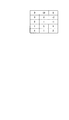
- FIG. 4 is an example of a table showing the amplitude value of the differential signal S corresponding to the combination of the data signal D and the internal signal CD used in determining the output amplitude.
- the amplitude value assignment of the differential signal S corresponding to the combination of the data signal D and the internal signal CD used in determining the output amplitude is not limited to the table shown in FIG.
- a binary differential output signal based on the data signal D and the internal signal CD determined based on the above table is output from the binary differential signal output circuit 11 as a differential signal S.
- FIG. 5 is a diagram showing the signal timing of the signal transmission method shown in FIG. 3 and the waveform of the binary differential output signal.
- the differential signal S is different from a fixed pattern in which the amplitude is fixed, such as the clock signal CK, and has four amplitudes (the absolute value of the amplitude).
- this differential signal S is an advantageous signal as an EMI generation source.
- the number of signals is reduced by half in comparison with the configuration of the signal transmission method in the first embodiment shown in FIG. This is a very useful signal transmission system for reducing the total EMI energy.
- the second embodiment does not prescribe each amplitude value of multi-value amplitude modulation.
- a characteristic part of the second embodiment is that the data signal D (serial data) and the clock signal CK as described above are transmitted in multi-values, and the amplitude value is realized by a transmission path and a receiving circuit. It is possible to set an appropriate value by design such as the above, and it does not limit the realization of the second embodiment.
- the transmitted differential signal S is inversely converted by the binary differential signal receiving circuit 12 from the amplitude value according to the table of FIG. .
- the inversely converted data signal DO is the transmitted data signal D itself.
- the inversely converted data signal DO and the internal signal CDO are calculated by the exclusive OR circuit 13, and as a result, the transmission clock signal CKO is reproduced.
- the clock signal CKO is multiplied by the PLL 15 to generate a sampling CK (sampling clock) of the data signal DO (serial data).
- the two signals of the data signal D and the clock signal CK are transmitted as a pair of differential signals S.
- the differential signal S can be a signal in which the spectrum peak of the signal is reduced compared to a signal having a regular amplitude such as the clock signal CK. Therefore, EMI due to the differential signal S can be further suppressed while maintaining the effect of the first embodiment.
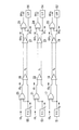
- FIGS. 6A to 8B are diagrams illustrating a configuration example of a signal transmission method according to the third embodiment of the present invention.
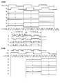
- FIG. 7 is a diagram showing signal timings of the signal transmission method shown in FIGS. 6A to 6C and waveforms of binary differential output signals.
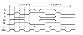
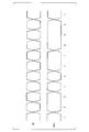
- 8A and 8B show a plurality of data signals DO 0 to DO 2 and clock signals CKO 0 to CKO 2 reproduced on the receiving side and data signals DO 0 to DO 2 (serial data) on the receiving side. It is a figure which shows the signal timing of the reproduction
- the signal transmission method of the third embodiment is composed of three transmission data lanes provided corresponding to the differential signals S 0 to S 2 .
- the case where there are three transmission data lanes is shown, but this is an example, and the number of transmission data lanes is not limited.
- a 6-bit data signal is converted into serial data, the converted serial data is superimposed on a clock signal, and the superimposed signal is multivalued (this In the configuration example, the differential signal is transmitted with a four-value amplitude (the absolute value of the amplitude is two).
- the characteristic part is different from the first embodiment (see FIG. 1) and the second embodiment (see FIG. 3) on the receiving side, and does not require a PLL circuit. That is. This will be described in detail in the operation description.
- numerals 17, 20, 21, 24, 25 and 28 are exclusive OR circuits
- numerals 18, 22 and 26 are binary (amplitude) differential signal output circuits
- numerals 19, 23 and 27 are binary.
- Differential signal receiving circuits symbols S 0 , S 1 and S 2 indicate differential signals, respectively.
- Reference numerals 51, 53 and 55 denote parallel-serial conversion blocks
- reference numerals 52, 54 and 56 denote serial-parallel conversion blocks.
- FIG. 6C shows a circuit configuration of the serial / parallel conversion blocks 52, 54, and 56 in the signal processing unit on the reception side.
- FIG. 6C shows the circuit configuration of the serial / parallel conversion block 52, and the circuit configurations of the other serial / parallel conversion blocks 54 and 56 are the same as those of the serial / parallel conversion block 52.
- FIG. 6B shows a logic circuit provided in common to the signal processing unit on the receiving side. The operation of the circuits shown in FIGS. 6B and 6C will be described in detail together with the operation on the reception side after the operation on the transmission side of the signal transmission method shown in FIG. 6A is described.
- the transmission data lane for transmitting the differential signal S 0 is the first transmission data lane
- the transmission data lane for transmitting the differential signal S 1 is the second transmission data lane
- the transmission data lane for transmitting the differential signal S 2 is the transmission data lane.
- This will be described as the third transmission data lane.
- the parallel / serial converted data signal D 0 is input to one of the binary differential signal output circuits 18.
- the clock signal CK 0 is subjected to an exclusive OR operation with the data signal D 0 by the exclusive OR circuit 17.
- Calculation result signal is an internal signal CD 0.
- This internal signal CD 0 is input to the other side of the binary differential signal output circuit 18.
- Binary differential signal output circuit 18 uniquely determines the output amplitude by a combination of the data signals D 0 and an internal signal CD 0 of the input signal, and outputs a differential multilevel signal S 0.
- the parallel / serial converted data signal D 1 is exclusively ORed with the clock signal CK 1 by the exclusive OR circuit 21.
- Calculation result signal is an internal signal CD 1.
- This internal signal CD 1 is input to one of the binary differential signal output circuits 22.
- Binary differential signal output circuit 22 is uniquely determines an output amplitude by a combination of the data signals D 1 and the internal signal CD 1 of the input signal, and outputs a differential multilevel signal S 1.
- the parallel / serial converted data signal D 2 is exclusively ORed with the clock signal CK 2 by the exclusive OR circuit 25.
- Calculation result signal is an internal signal CD 2.
- the internal signal CD 2 is input to the other side of the binary differential signal output circuit 26.
- Binary differential signal output circuit 26 uniquely determines the output amplitude by a combination of the data signal D 2 and the internal signal CD 2 of the input signal, and outputs a differential multilevel signal S 2.
- the table for determining the output amplitude in each transmission data lane the table illustrated in FIG. 4 used in the second embodiment can be used.
- the assignment of binary amplitude conversion is not limited to the table shown in FIG.
- FIG. 7 shows a signal transmission time table determined in this way.
- FIG. 7 is a diagram showing the signal timing and the waveform of the binary differential output signal of the signal transmission method shown in FIGS. 6A to 6C.
- each differential signal to be transmitted is not a fixed pattern like the clock signal CK.
- This is a differential signal having a four-value amplitude (binary as the absolute value of the amplitude), and this differential signal is an advantageous signal as an EMI generation source.
- three systems of serial data and a clock signal can be transmitted by three differential signals (multilevel differential signals S 0 to S 2 ).
- Differential signal S 0 transmitted, S 1, S 2 is the differential signal receiver circuit 19,23,27, according to the table shown in FIG. 4 described above, the internal signal CD 0 of the receiving side of the amplitude, CD 1 , CD 2 and data signals D 0 , D 1 , D 2 are inversely converted.
- the inversely converted data signals DO 0 , DO 1 , DO 2 are the transmitted data signals D 0 , D 1 , D 2 themselves.
- the data signals DO 0 , DO 1 , DO 2 and the inversely converted internal signals CDO 0 , CDO 1 , CDO 2 are calculated by the exclusive OR circuits 20, 24, 28, respectively, and transmitted as a result.
- Clock signals CK 0, CK 1 and CK 2 are reproduced as clock signals CKO 0 , CKO 1 and CKO 2 .
- the clock signals CK 0, CK 1, and CK 2 to be transmitted are clocks of parallel data rates, and are respectively signals whose phases are shifted by 1/6 (60 degrees) (the fourth to sixth stages in FIG. 8A). Waveform reference).
- the phase shift method is as follows: the clock signal CK generation unit 7c in the transmission side signal processing unit of each transmission data lane is shifted by a period corresponding to one cycle at the rising edge of the shift clock between the transmission data lanes. It is possible by shifting the clock and generating.
- the receiving side generates the sampling clock (CKO) shown in the fourth stage of FIG. 8B from each edge of the regenerated clock signals (clock signals CKO 0 , CKO 1 , CKO 2 ). This facilitates the use of the PLL circuit used in the first and second embodiments.
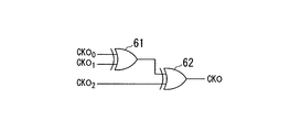
- the first to third transmission data lanes have the logic (logic circuit) shown in FIG. 6B in common.
- this logic includes an exclusive OR circuit 61 and an exclusive OR circuit 62.
- the exclusive OR circuit 61 receives the clock signal CKO0 reproduced by the exclusive OR circuit 20 of the first transmission data lane and the clock signal CKO1 reproduced by the exclusive OR circuit 24 of the second transmission data lane. Is done.
- the exclusive OR circuit 62 receives the output of the exclusive OR circuit 61 and the clock signal CKO2 reproduced by the exclusive OR circuit 28 of the third transmission data lane, and outputs a sampling clock (CKO) ( (Refer to the fourth CKO waveform in FIG. 8B).
- the serial / parallel conversion block in each transmission data lane uses the sampling clock (CKO) and the clock signals (clock signals CKO 0 , CKO 1 , CKO 2 ) reproduced in each transmission data lane to generate data signals DO 0 , DO 1 , DO. 2 (Serial data) is converted to parallel data.
- FIG. 6C is a circuit configuration diagram of the serial-parallel conversion block 52 on the receiving side of the first transmission data lane.
- the serial / parallel conversion block 52 includes a shift register unit 63a, a shift register unit 63b, and a data load unit 63c.
- serial-parallel conversion block 54 on the reception side of the second transmission data lane and the serial-parallel conversion block 56 on the reception side of the third transmission data lane are also the serial-parallel conversion block 52 on the reception side of the first transmission data lane.
- the circuit configuration is the same as that shown in FIG.
- Each latch circuits constituting a shift register unit 63a captures the data signals DO 0 from the preceding stage at the falling of the sampling clock (CKO), each data constituting the next stage of the latch circuit at the next rising, and the data loading unit Data signal DO 0 is output to the load. Further, each of the latch circuits constituting a shift register unit 63b captures the data signals DO 0 from the previous stage in the rising of the sampling clock (CKO), constituting the next stage of the latch circuit at the next falling edge, and the data loading unit Output data signal DO 0 to each data load.
- the shift register unit 63a takes in the first data signal DO 0_0 of the reproduced data signal DO 0 (shown in the fifth stage of FIG. 8B) at the first falling edge of the sampling clock (CKO). Then, at the rise of the third sampling clock (CKO), the data signal DO 0 — 0 is output from the third stage latch circuit to the data load (refer to the waveform indicated by DO 0 — 0 at the eleventh stage in FIG. 8B).
- the shift register unit 63b takes in the second data signal DO 0_1 of the reproduced data signal DO 0 at the second rising edge of the sampling clock (CKO), and from there the third sampling clock (CKO) At the falling edge, the data signal DO 0_1 is output from the third-stage latch circuit to the data load (refer to the waveform indicated by DO 0_1 at the 10th stage in FIG. 8B).
- the shift register unit 63a captures the third data signal DO 0_2 of the reproduced data signal DO 0 at the falling edge of the next sampling clock (CKO) that captures the first data signal DO 0_0 . Then, at the rise of the second sampling clock (CKO), the data signal DO 0_2 is output from the second stage latch circuit to the data load (see the waveform indicated by DO 0_2 at the ninth stage in FIG. 8B).
- the shift register unit 63b a fourth data signal DO 0_3 of the reproduced data signals DO 0, the rise in uptake of the next second data signal DO 0_1 the accepted sampling clock (CKO), from which 2 At the falling edge of the second sampling clock (CKO), the data signal DO 0 — 3 is output from the second-stage latch circuit to the data load (see the waveform indicated by DO 0 — 3 on the eighth stage in FIG. 8B).
- the shift register unit 63a the fifth data signal DO 0_4 of the data signals DO 0 reproduced captures the falling edge of the third captured data signal DO 0_2 next sampling clock (CKO), the following At the rising edge of the sampling clock (CKO), the data signal DO 0_4 is output from the first-stage latch circuit to the data load (see the waveform indicated by DO 0_4 at the seventh stage in FIG. 8B).
- the shift register unit 63b captures the sixth data signal DO 0_5 of the reproduced data signal DO 0 at the next rising edge of the sampling clock (CKO) that captures the fourth data signal DO 0_3, and performs the next sampling.
- the data signal DO 0_5 is output from the first-stage latch circuit to the data load (see the waveform indicated by DO 0_5 at the sixth stage in FIG. 8B).
- the data load unit 63c on the reception side of the first transmission data lane receives a data signal (data signal) from each data load at the rising edge of the data load clock (reproduced clock signal CKO 1 ) input from the exclusive OR circuit 20.
- D 0 — 0 to D 0 — 5 are output to the outside of the signal processing unit at a parallel data rate (see signals shown in the 12th to final stages in FIG. 8B).
- the data load units on the reception side of the second transmission data lane and the third transmission data lane also each receive a plurality of data signals (not shown) input to the transmission side at the parallel data rate. Output to the outside.
- the clock signals CK 0, CK 1, CK 2 and the data signals D 0 , D 1 , D 2 can be transmitted as three pairs of differential signals, Instead of a regular signal such as the clock signal CK, the spectrum peak can be reduced and the number of signals can be reduced.
- the number of signals can be realized by a differential signal pair that is half the total number of signals to be transmitted (the total number of serial data and superposed clock signals).
- the sampling clock for serial data can be easily generated by simple logic (circuit shown in FIG. 6B) as described above.
- the PLL circuit for multiplying the sampling clock required in the first embodiment and the second embodiment by the clock signal is unnecessary, and transmission is performed. It is possible to realize a reduction in the circuit scale of the circuits constituting the data lane and low power consumption when the transmission data lane operates.
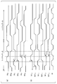
- FIG. 9 shows signal timing and four amplitudes when the DC balance improvement method for AC coupled transmission is applied in the signal transmission method shown in FIGS. 6A to 6C (the absolute value of the amplitude is binary). It is a figure which shows the waveform of a differential output signal.
- FIG. 10 is a diagram showing the timing of the regenerated data and CK of the signal transmission method shown in FIG.
- the clock signal itself is superimposed on the data signal, and the transmission of the clock signal itself is eliminated, so that the effect of reducing EMI can be expected.
- the superimposed data signal and clock signal are basically random signals.
- the first to third embodiments are basically based on generating transmission data by exclusive OR operation of a clock signal and a data signal as a signal to be transmitted. Therefore, when the same “0” or “1” data pattern as the clock signal continues, the transmission signal becomes a DC output during that time. There is no problem when transmission and reception are directly connected, but it is a problem when adapting to AC coupling.
- a signal transmission method capable of AC coupling even in such a case is shown.
- a case where 3 bits of continuous data composed of “1”, “0”, and “1” are inserted every 6 bits of serial data will be described.
- the exclusive OR of the data signal and the clock signal of the parallel data is obtained, thereby “1” “0”.
- are always generated see the differential signals S 0 to S 2 in FIG. 9). Therefore, there is always data inversion every 6 bits, the generation of a DC pattern can be suppressed to 6 bits or less, and DC balance improvement for AC coupled transmission can be realized.
- the insertion data (transmission data composed of “1”, “0”, “1”) is transmitted from the signal processing unit in the transmission unit after the parallel-to-serial conversion operation of the data signal.
- the transmission side exclusive OR circuit exclusive OR circuits 17, 21 and 25 shown in FIGS. 6A to 6C) provided in FIG. 6 is transmitted instead of the parallel-serial conversion blocks 51, 53 and 55. Good.
- the receiving side uses the recovered clock signals (clock signals CKO 0 , CKO 1 , CKO 2 ), for example, in the same way as the means in the third embodiment (circuits shown in FIGS. 6B and 6C). (Denoted by CK in FIG. 10) is generated, and the data signals DO 0 , DO 1 , DO 2 (serial data) may be converted into parallel data.
- FIG. 11 is a circuit configuration diagram of a binary differential signal output circuit for controlling the amplitude of a differential signal.
- FIG. 12 is a circuit configuration diagram of the differential signal receiving circuit in the case of controlling the amplitude of the differential signal.
- QN1 to QN8 are MOS transistors, and RT is a termination resistor for differential signals.
- the binary differential signal output circuit of FIG. 11 controls the direction of the current flowing through the termination resistor RT by the signals input from the terminals 101 and 102.
- the amplitude of the differential signal is determined by the value of the termination resistor RT and the value of current flowing therethrough.
- the current flowing through the termination resistor RT is determined by the Bias voltage value input from the transistors QN7 and QN8 and the terminal 104.
- the center voltage (common voltage) of the differential signal is determined by QN5 and the Bias voltage input from the terminal 105. Normally, this voltage is controlled to be a fixed common voltage by monitoring the differential output voltage and performing feedback control. Since this control is not a characteristic part of the fourth embodiment, a detailed description thereof will be omitted.
- the clock signal CK is input to the input terminal 101 and the inverted signal CKB of the clock is input to the input terminal 102.
- the switch including the transistors including QN1 to QN4 operates as follows. That is, QN2 and QN3 are turned on, and QN1 and QN4 are turned off. At this time, the current flowing through the termination resistor RT flows from the terminal 106 to the terminal 107. Conversely, when the clock signal CK is L and the inverted signal CKB is H, QN2 and QN3 are turned OFF, and QN1 and QN4 are turned ON. At this time, the current flowing through the termination resistor RT flows from the terminal 107 to the terminal 106. In this way, the direction of the differential signal is controlled by the clock signal.
- the amplitude of the differential signal is determined by QN7 and QN8 as described above.
- a data signal is input from the terminal 103 to the gate of QN6.
- QN6 operates as a switch and controls the current value flowing through the termination resistor RT. Basically, the Bias voltage input from the terminal 104 and the current value ID determined by QN7 flow through the termination resistor RT. When the data signal is 0, QN6 is OFF, and the current flowing through the termination resistor RT is the current value ID.
- the binary differential signal output circuit for controlling the amplitude of the differential signal in the second to fourth embodiments described above can be realized.
- This binary differential signal output circuit controls the current values ID and ID2 by controlling the bias voltage input to the terminal 104 and the bias voltage input to the terminal 105, thereby controlling the amplitude. It becomes possible.
- the differential signal receiving circuit includes a differential amplifier 110, a differential amplifier 111, a differential amplifier 112, and an AND gate 133.
- the differential reception signals SO + and SO ⁇ are input to the differential amplifier 111.
- the output from the differential amplifier 111 is a signal whose polarity is inverted depending on the signal direction regardless of the amplitude of the differential signal. That is, the data signal DO according to the table shown in FIG. 4 described above is output.
- the differential reception signal SO + is input to the comparator 110, and the other input of the comparator 110 is input with the determination threshold VrefU having a large amplitude.
- the comparator 110 compares the two input signals and outputs H when the differential reception signal SO + is greater than the determination threshold value VrefU.
- the differential reception signal SO ⁇ is input to the comparator 112, and the other input of the comparator 112 is input with a determination threshold VrefD having a large amplitude.
- the comparator 112 compares the two input signals, and outputs H when the differential reception signal SO ⁇ is smaller than VrefD.
- the outputs of the comparators 110 and 112 are input to the AND gate 113.
- the AND gate 113 outputs H when the input amplitude of the differential signal is large, that is, when the differential reception signal SO + is larger than the determination threshold value VrefU and the differential reception signal SO ⁇ is smaller than the determination threshold value VrefD. To do.
- the AND gate 113 Is output. In this way, the internal signal CDO obtained by reproducing the internal signal CD is output from the differential signal receiving circuit.
- the determination level of the differential signal receiving circuit can be changed by controlling the voltage levels of the determination values VrefD and VrefU according to the amplitude of the differential signal.
- a fifth embodiment of the present invention will be described with reference to FIG.
- a lane transmission / reception lane
- the signal transmission scheme shown in FIG. 13 is a signal transmission scheme in which a two-line transmission path capable of bidirectionally transmitting and receiving data is added to the above-described third embodiment (see FIGS. 6A to 6C).
- reference numerals 31, 34, 35, 38, 39, and 42 are exclusive OR circuits
- reference numerals 32, 36, and 40 are binary amplitude differential signal transmission circuits
- reference numerals 33, 37, and 41 are binary amplitude differences.
- Reference numerals 29 and 30 are transmission / reception circuits for bidirectional two-wire signals (bidirectional control lines).
- the bidirectional control line can be realized by a control method represented by an I2C signal, for example.
- the control method for realizing the bidirectional control line is not limited, and any means can be used as long as the bidirectional reception function can be realized.
- a bidirectional data signal system transmission / reception lane
- a control signal to be transmitted it is possible to facilitate processing of received data on the receiving side by transmitting information on a data signal to be transmitted as a differential data signal.
- the signal to be transmitted as differential data is a video signal
- the information on the video signal format to be transmitted (such as the number of pixels) is transmitted, so that processing according to the video signal format can be appropriately performed on the receiving side.
- skew control for adjusting the timing of sampling the data signal on the receiving side, or a clock signal (parallel data rate of the parallel data rate) superimposed on the data signal on the transmitting side.
- skew control for adjusting the output timing of the clock.
- FIG. 14 shows a circuit configuration on the reception side for performing the skew control
- FIG. 15 shows a circuit configuration on the transmission side.
- FIG. 14 shows an example of a circuit configuration when skew control is performed on the receiving side in the fifth embodiment.
- reference numeral 43 is a differential signal receiving circuit
- reference numeral 44 is an exclusive OR circuit
- reference numeral 45 is a skew control circuit
- reference numeral 46 is a receiving register.
- the regenerated clock signal CKO is controlled as a clock signal CKd by controlling the delay time by the skew control circuit 45 and input to the receiving register 46.
- the sampling timing of the data signal DO can be adjusted to the optimum sampling timing (for example, the central portion of each bit between the switching of bits in the serial data).
- FIG. 15 shows a circuit configuration example when skew control is performed on the transmission side in the fifth embodiment.
- reference numeral 49 is a transmission circuit
- reference numeral 48 is an exclusive OR circuit
- reference numeral 47 is a skew control circuit.
- CK parallel data rate clock
- CKd is controlled as a clock signal CKd by controlling the delay time by the skew control circuit 47 and input to the exclusive OR circuit 48.
- the sampling timing of the data signal DO can be adjusted to the optimum sampling timing in the same manner as the adjustment on the receiving side.
- FIG. 16 is a diagram illustrating a signal transmission method for explaining the skew control.
- FIG. 17 is a timing chart for explaining the skew control operation.
- the transmission signal system shown in FIG. 16 has a configuration in which skew control circuits 71 to 76 are provided in the transmission signal system shown in FIG.
- the skew control circuit 71 for performing skew control of the post-reproduction data signal DO 0 and the skew control for performing skew control of the post-reproduction clock signal CKO 0 A circuit 72 is provided in the first transmission data lane for transmitting the differential signal S 0 .
- the skew control circuit 73 for controlling the skew of the post-reproduction data signal DO 1 and the skew control of the post-reproduction clock signal CKO 1 are performed in the second transmission data lane for transmitting the differential signal S 1 .
- a skew control circuit 74 is provided in the second transmission data lane for transmitting the differential signal S 1 .
- each skew control circuit is a delay value (delay time) set in each skew control circuit by the test operation described below.
- the data signals superimposed in pairs with the clock signal have the same skew (for example, the serial data after reproduction shown in the first stage is the parallel rate shown in the second stage). Included in one period of the clock signal).
- the transmission side transmits a clock signal with a phase difference for each transmission data lane
- the regenerated clock signal wiring is different for each transmission data lane. Therefore, a different delay difference occurs in the clock signal after reproduction, and a phase difference different from the phase difference given between the clock signals on the transmission side may occur between the clock signals after reproduction. This is not preferable when the sampling signal is generated by taking the logic of the clock signal after reproduction as in the third embodiment.
- a delay time is set in each skew control circuit, and the clock signal after reproduction and the data signal (serial data) after reproduction are predetermined (provided on the transmission side) between transmission data lanes. Control to return to the phase difference.
- FIG. 17A shows that the data signal DO 1 after reproduction in the second transmission data lane and the clock signal CKO 1 after reproduction are the data signal DO 0 after reproduction and the clock after reproduction in the first transmission data lane. This shows a case where a delay difference is generated for the signal CKO 0 by the time t1.
- FIG. 17A shows the data signal DO 2 after reproduction in the third transmission data lane and the clock signal CKO 2 after reproduction in the data signal DO 0 after reproduction in the first transmission data lane and after reproduction. This shows a case where a delay difference is generated with respect to the clock signal CKO 0 of time t2 by time t2.
- an optimum delay time is determined in the test operation in order to eliminate this delay difference.
- the reproduced data signal DO 0 and the reproduced clock signal CKO 0 in the first transmission data lane are given to the skew control circuits 71 and 72, and the delay time t1 is given. By setting, it is delayed by time t1.
- the reproduction data signal DO 2 and the reproduction clock signal CKO 2 in the third transmission data lane are delayed by the time (t 1 + t 2) by setting the delay time (t 1 + t 2) in the skew control circuits 75 and 76.
- information for transmitting a TEST pattern from the transmission side using the bidirectional control lines S_CK and S_D (a test start signal from the transmission side to the reception side indicating that a plurality of data signals are transmitted through the transmission data lane) ) Is transmitted to the receiving side (step 1).
- the receiving side receives the information and prepares to receive a test pattern. That is, the reception side sets the delay time of each skew control circuit (second skew adjustment circuit) (step 2). After setting the delay time, the reception side transmits a test preparation completion signal to the transmission side using the transmission / reception lane after completion of reception preparation of the test pattern (step 3).
- the transmitting side transmits the next determined TEST pattern (a plurality of data signals) (step 4).
- the receiving side collates the reception pattern with a preset TEST pattern (step 5). At this time, skew control on the receiving side, for example, the delay value shown in FIG. 16 is changed, and pattern matching is performed to obtain an optimum value of matching values. That is, the above steps 2 to 5 are executed until the TEST pattern received in step 5 matches the preset TEST pattern. When the optimum value of the delay time is determined, the receiving side returns the information to the transmitting side through the bi-directional control line and ends the sequence (step 6).
- FIG. 18 is a diagram illustrating a signal transmission method when skew control is performed on the transmission side.
- the skew control circuit provided on the transmission side is omitted, but for example, the circuit shown in FIG. 15 can be used as the skew control circuit.
- the transmission side delay (the delay amount of the skew control circuit 47 in FIG. 15) is controlled in the same manner as in the signal transmission method shown in FIG. That is, first, the transmission side transmits a test start signal using the transmission / reception lane (step 1). Subsequently, the transmission side sets the delay time of the skew control circuit 47 (first skew adjustment circuit) in each transmission data lane (step 2). The reception side transmits a test preparation completion signal to the transmission side using the transmission / reception lane (step 3). Next, in response to the completion of test preparation, the transmission side transmits test patterns stored in advance by the reception side to a plurality of transmission data lanes (step 4).
- the receiving side compares the TEST pattern received via the plurality of transmission data lanes with the TEST pattern stored in advance (step 5).
- the transmitting side changes the delay time of the skew control circuit in step 2, and the transmitting side or the receiving side sequentially executes step 2 to step 5, and if the comparison results match in step 5, the receiving side A test end signal is transmitted using the lane (step 6).
- an example of amplitude control in the binary differential signal output circuit shown in FIG. 11 and threshold control in the differential signal reception circuit shown in FIG. In the same manner as described above, the test pattern is transmitted at the basic transmission amplitude, and the threshold value of the differential signal receiving circuit is controlled to control the value that matches the pattern. Next, the transmission amplitude is changed and the same test is performed to determine the threshold value of the differential signal receiving circuit. These controls are repeated to determine the amplitude and threshold value that can be reliably received with the smallest amplitude.
- the transmission side transmits a test start signal using the transmission / reception lane (step 1).
- the receiving side sets a determination threshold value of the differential signal receiving circuit provided on the receiving side (step 2).
- the transmission side sets the amplitude of the differential signal of the transmission circuit provided on the transmission side (step 3).
- the reception side transmits a test preparation completion signal to the transmission side using the transmission / reception lane (step 4).
- the transmission side transmits a test pattern stored in advance by the reception side to a plurality of transmission data lanes (step 5).
- the receiving side compares the TEST pattern received via the plurality of transmission data lanes with the TEST pattern stored in advance (step 6).
- the receiving side changes the determination threshold value in step 2 above. Thereafter, the receiving side or the transmitting side sequentially executes step 2 and steps 4 to 6 described above. If the comparison result matches in step 6, the transmission side changes the amplitude in step 3. Thereafter, the receiving side or the transmitting side sequentially executes the above steps 3 to 6. If the comparison results match in the process of step 6, the receiving side transmits a test end signal using the transmission / reception lane (step 7).
- the signal transmission method of the third embodiment and the signal transmission of the fourth embodiment are made more effective by adding control lines (transmission and reception lanes) as described above. It can be realized.
- the main point of each embodiment of the present invention is to solve the following problem, and presents a problem solving means for achieving the problem, and is characterized by its effects.
- the bandwidth of signals to be transmitted tends to increase with the improvement of digital TV image quality, and the current system is approaching the limits of the number of signals, clock skew, etc.
- LSI power consumption, chip surface properties Both increase and become a cause of noise generation such as EMI. Therefore, in the fifth embodiment, an attempt is made to realize a signal transmission system for a differential signal with less generation of EMI noise while ensuring the skew margin while ensuring the transmission of an increasing digital video signal with a smaller number of signal lines. It is.
- the clock signal is randomized by taking the EXOR of the clock signal and the data signal to be transmitted, and the clock signal can be easily reproduced by inversely transforming with the EXOR on the receiving side.
- EMI is reduced by data transmission.
- a parallel data rate clock as the clock signal to be superimposed on the data signal
- the frequency and energy of the clock superimposed on the data signal can be reduced without lowering the transfer rate of the plurality of data signals.
- EMI reduction in the differential drive method can be achieved.
- the number of signals can be reduced by, for example, parallel / serial conversion and transmission of the data signal.
- two signals of a data signal and a clock signal are transmitted as a pair of differential signals S. Since the differential signal S is not a signal having a regular amplitude like the clock signal CK, and the spectrum peak of the signal can be reduced, EMI due to the differential signal S can be further suppressed. In addition, according to the signal transmission method of the second embodiment, it is possible to reduce the number of differentially amplified signals.
- a clock signal having a phase shifted for each transmission lane is superimposed on the data signal, and a sampling clock for easily sampling serial data with simple logic on the reception side is provided.
- serial data sampling can be realized without a PLL, and the circuit scale of the transmission data lane can be reduced, and low power consumption when the transmission data lane operates can be realized.
- a bidirectional transmission / reception lane is provided separately from a plurality of transmission data lanes, and a control signal is transmitted and received between the transmission side and the reception side in the transmission / reception lane.
- a control signal is transmitted and received between the transmission side and the reception side in the transmission / reception lane.
- the present invention can be applied to a signal transmission system for reducing EMI in a differential drive system by reducing the frequency and energy of a clock superimposed on a data signal.
Landscapes
- Engineering & Computer Science (AREA)
- Computer Networks & Wireless Communication (AREA)
- Signal Processing (AREA)
- Dc Digital Transmission (AREA)
- Synchronisation In Digital Transmission Systems (AREA)
- Cable Transmission Systems, Equalization Of Radio And Reduction Of Echo (AREA)
Abstract
信号伝送方式は、クロック信号と複数のデータ信号とを重畳した信号を、正負二つの差動信号によって伝送し、クロック信号は、伝送すべき複数のデータ信号各々の転送レートを規定する基準クロック信号であり、複数のデータをクロック信号の転送レートで送信する。
Description
本発明は、信号伝送方式及び送信装置に関する。
本願は、2011年5月12日に、日本に出願された特願2011-107496号に基づき優先権を主張し、その内容をここに援用する。
本願は、2011年5月12日に、日本に出願された特願2011-107496号に基づき優先権を主張し、その内容をここに援用する。
従来、液晶表示パネル等の表示装置を駆動するドライバ部と、ドライバ部にデータを送信するタイミング制御部との間の伝送において、RSDS(Reduced Swing Differential Signaling)などの差動駆動方式が用いられている。また、主に映像信号等を、半導体集積回路間で伝送する際、或いは信号処理回路基板及び機器間で伝送する際、LVDS(Low Voltage Differential Signaling)などの差動駆動方式が用いられている。
このような差動駆動方式は、一つの信号を、極性が反対となる一対の差動信号として二つの信号線で伝送する方式である。そのため、かかる差動駆動方式においては、受信部は一対の差動信号のレベル差で送信部からの差動信号を認識し、個々の信号線の振幅の倍を有する振幅の信号として差動信号を認識できる。つまり、差動駆動方式では、個々の信号線の振幅を小さくすることができる。このように、差動駆動方式においては、信号線の振幅を小さくすることができるため、差動信号線から発生する電磁波エネルギーを小さくすることができる。また、差動駆動方式においては、差動信号が対になっているので、信号線から発生する電磁波が互いに打ち消しあう。そのため、差動駆動方式において、EMI(Electro Magnetic Interference:電磁波干渉)が削減される。また、差動増幅方式は、受信部が一対の差動信号のレベル差で信号を認識するので、ある程度ノイズにも強い。
図20は、上述した従来の差動信号伝送におけるクロック信号CKとデータ信号Dataの信号形態を示す図である。差動駆動方式において、図20に示すクロック信号CKとデータ信号Dataとを送信ため、少なくとも二対の差動伝送線が必要となる。また、差動駆動方式において、送信部と受信部のインターフェースレベルが異なる場合、あるいはGNDレベルが異なる場合など、受信部における信号接続に関して、コンデンサを介してAC結合で接続される場合が多く存在する。AC結合で接続される場合、受信部と送信部はコンデンサを介して接続されるため、差動信号のDC成分は伝達されない。AC結合の場合に、正しく差動信号を伝達するためには、DC的にバランスした信号(0と1が等しい個数)にする必要がある、このため、一般には8B10B等のエンコードを用いる必要が生じる。
なお、差動信号伝送方式における信号伝送を多重化する従来技術は、例えば、特許文献1において開示されている。この特許文献1が開示する差動駆動方式を採用すれば、信号の伝送レートは2倍になるが、AC結合で接続され場合に対応するには、データのエンコードが必要となる。なお、クロック信号の信号伝送方式については、特許文献1には開示されていない。
上述したように、図20に示すような従来の差動信号伝送方式においては、少なくともデータ信号Dataとクロック信号CKとを伝送する2対の信号線が必要であった。しかしながら、近年のシステムにおいてはより多量のデータを並列に伝送する必要があり、従来の差動信号伝送方式においては信号線の数が非常に多くなってしまうという問題があった。
また、EMIの発生源としては伝送配線でのコネクタやケーブルからの放射が考えられるが、これらの基となるノイズは伝送する信号に依存する。特に、クロック信号は信号が0に対応する値と1に対応する値との間でスイッチングする回数も多く、クロック信号の周波数及び高調波に大きなスペクトル成分を持つことになる。このようなクロック信号が有するエネルギーが、コネクタ、ケーブル、基板等から放射されて、EMIの発生源として問題となる。
しかし、特許文献1に示すような多重方式は、上述した通り、クロック信号の多重方式については記載されておらず、基本的にはクロック信号の伝送を必要とするシステムとなっている。さらに、AC結合接続をする場合、DCバランスを保つようなエンコード(8B10B等)が必要となり、回路構成が複雑化するという問題が生じてしまう。
しかし、特許文献1に示すような多重方式は、上述した通り、クロック信号の多重方式については記載されておらず、基本的にはクロック信号の伝送を必要とするシステムとなっている。さらに、AC結合接続をする場合、DCバランスを保つようなエンコード(8B10B等)が必要となり、回路構成が複雑化するという問題が生じてしまう。
このような問題を解決するために、本願発明者は、特許文献2に示すように、より簡単な構成でクロックとデータの重畳、データ多重化を実現する方式を提案している。
特許文献2において開示した方式は、上述した問題を解決するため、クロック信号とデータ信号を多重し、容易にクロック再生でき且つAC結合伝送においてもエンコードなしでDCバランスのよい信号伝送を実現し、特にノイズ源となりやすいクロック信号を容易にノイズピークの低い伝送信号として送信可能とする方式である。
特許文献2において開示した方式は、上述した問題を解決するため、クロック信号とデータ信号を多重し、容易にクロック再生でき且つAC結合伝送においてもエンコードなしでDCバランスのよい信号伝送を実現し、特にノイズ源となりやすいクロック信号を容易にノイズピークの低い伝送信号として送信可能とする方式である。
しかし、この方式を用いて多量のデータを並列に伝送する場合、クロック信号とデータ信号とを重畳した差動信号の配線数も増え、重畳されるクロック信号によるEMI増大を抑制することができなくなるという問題がある。
本発明は、上記差動駆動方式の効果を維持しつつ、さらに、複数のデータ信号の転送レートを下げずに、データ信号に重畳するクロック信号の周波数を低減することを主要な課題とする。
(1) 本発明の第1の態様は、クロック信号と複数のデータ信号とを重畳した信号を、正負二つの差動信号によって伝送し、前記クロック信号は、伝送すべき前記複数のデータ信号各々の転送レートを規定する基準クロック信号であり、前記複数のデータを前記クロック信号の転送レートで送信する信号伝送方式である。
(2) 本発明の第1の態様において、前記複数のデータ信号をパラレルシリアル変換して、変換後のシリアルデータを前記クロック信号の前記転送レートで送信しても良い。
(3) 本発明の第1の態様において、前記クロック信号と前記複数のデータ信号との排他的論理和の信号と、前記複数のデータ信号を、別の信号線ペアを用いてそれぞれ差動信号で伝送しても良い。
(4) 本発明の第1の態様において、前記クロック信号と前記複数のデータ信号との排他的論理和の信号と、前記複数のデータ信号とを多重化し、多重化した信号を1対の信号線ペアを用いて、多値の振幅をもつ差動信号で伝送しても良い。
(5) 本発明の第1の態様において、前記多値の振幅を、予め設定されたテーブルに基づいて設定しても良い。
(6) 本発明の第1の態様において、前記シリアルデータ毎に、0及び1の連続したデータを付加して伝送しても良い。
(7) 本発明の第1の態様において、前記複数のデータ信号を複数のデータブロックに分割し、前記クロック信号と前記複数のデータブロックを転送する複数の送信データレーン毎に、前記クロック信号の位相を変えて前記データブロックを伝送しても良い。
(8) 本発明の第1の態様において、受信側において、前記複数の送信データレーン毎に、送信側から送出される差動信号に基づいて前記クロック信号を再生し、前記複数の送信データレーン毎に再生されたクロック信号の論理の組合せに基づいてサンプリングクロックを生成し、生成したサンプリングクロックに基づいて、前記複数のデータ信号をサンプリングしても良い。
(9) 本発明の第1の態様において、送信側において、前記クロック信号を第1のスキュー制御回路により遅延させ、当該遅延させたクロック信号に応じて前記排他的論理和の信号を送信しても良い。
(10) 本発明の第1の態様において、受信側において、送信側から送出される差動信号に基づいて前記クロック信号を再生し、再生したクロック信号を第2のスキュー制御回路により遅延させ、当該遅延させたクロック信号に基づいて前記データ信号の論理の切り替わりの中央部において安定してサンプリングしても良い。
(11) 本発明の第1の態様において、前記複数の送信データレーン以外に設けられた送受信レーンを用いて、前記複数のデータ信号に関する情報を送受信しても良い。
(12) 本発明の第1の態様において、前記複数のデータ信号に関する情報は、前記複数のデータ信号を処理する際に用いる情報であっても良い。
(13) 本発明の第1の態様において、送信側が前記第1のスキュー調整回路の遅延時間を設定する、或いは受信側が前記第2のスキュー調整回路の遅延時間を設定しても良い。
(14) 本発明の第1の態様において、受信側に設けられた受信回路の判定しきい値を設定し、送信側に設けられた送信回路の前記差動信号の振幅を設定しても良い。
(15) 本発明の第1の態様において、前記差動信号を出力する送信回路は、差動信号を電流出力しても良い。
(16) 本発明の第2の態様は、クロック信号と複数のデータ信号とを重畳した信号を、正負二つの差動信号によって伝送する送信部を備え、前記クロック信号は、伝送すべき前記複数のデータ信号各々の転送レートを規定する基準クロック信号であり、前記送信部は、前記複数のデータを前記クロック信号の転送レートで送信する送信装置である。
本発明によれば、信号伝送方式において、複数のデータ信号の転送レートを下げずに、データ信号に重畳するクロック信号の周波数、エネルギーを低減することができ、差動駆動方式におけるEMI削減を図ることができる。
以下、図面を参照しながら本発明の第1~第5の実施形態を詳細に説明する。
[第1の実施形態]
図1(a)において、第1の実施形態の信号伝送方式は、送信側データ処理部1A、送信部1B、伝送部1C、受信部1D及び受信側データ処理部1Eを備える。さらに、送信側データ処理部1Aは、P/S変換部7を備える。送信部1Bは、排他的論理和回路1、差動信号出力回路2、3を備える。伝送部1Cは、伝送路10、11を備える。受信部1Dは、差動信号受信回路4、5、排他的論理和回路6を備える。また、受信側データ処理部1Eは、位相同期部(PLL)8、S/P変換部9を備える。
[第1の実施形態]
図1(a)において、第1の実施形態の信号伝送方式は、送信側データ処理部1A、送信部1B、伝送部1C、受信部1D及び受信側データ処理部1Eを備える。さらに、送信側データ処理部1Aは、P/S変換部7を備える。送信部1Bは、排他的論理和回路1、差動信号出力回路2、3を備える。伝送部1Cは、伝送路10、11を備える。受信部1Dは、差動信号受信回路4、5、排他的論理和回路6を備える。また、受信側データ処理部1Eは、位相同期部(PLL)8、S/P変換部9を備える。
また、図1(a)において、CK及びCKOはクロック信号を示し、D及びDOはデータ信号を示し、CD及びCDOは内部信号を示し、S0、S1は差動信号を示す。
図1(b)は、図1(a)のP/S変換部(パラレルシリアル変換ブロック7)の詳細なブロック図である。また、図1(c)は、図1(a)のS/P変換部(シリアルパラレル変換ブロック9)の詳細なブロック図である。パラレルシリアル変換ブロック7は、データロード部7a、シフトレジスタ部7b、クロック信号CK生成部7cを備える。シリアルパラレル変換ブロック9は、シフトレジスタ部9a、データロード部9bを備える。なお、図1(b)及び図1(c)において、矢印A11は、データシフト方向を示している。
図1(b)は、図1(a)のP/S変換部(パラレルシリアル変換ブロック7)の詳細なブロック図である。また、図1(c)は、図1(a)のS/P変換部(シリアルパラレル変換ブロック9)の詳細なブロック図である。パラレルシリアル変換ブロック7は、データロード部7a、シフトレジスタ部7b、クロック信号CK生成部7cを備える。シリアルパラレル変換ブロック9は、シフトレジスタ部9a、データロード部9bを備える。なお、図1(b)及び図1(c)において、矢印A11は、データシフト方向を示している。
送信側において、データ信号Dは、差動信号出力回路3により差動信号S1として伝送路C1へ出力される。また、クロック信号CKは、排他的論理和回路1によりデータ信号Dと排他的論理和演算され、この排他的演算結果信号は内部信号CDとなって、差動信号出力回路2により差動信号S0として伝送路C0へ出力される。
一方、受信側において、伝送路C1を介して伝送された差動信号S1は、差動信号受信回路5によりシングルエンドの信号(データ信号DO)として再生される。また、伝送路C0を介して伝送された差動信号S0は、差動信号受信回路4によりシングルエンド信号(内部信号CDO)に変換され、差動信号受信回路5によりシングルエンド変換された信号(データ信号DO)と共に排他的論理和回路6に入力され、その排他的論理和回路6の演算結果(クロック信号CKO)が出力される。ここで、差動信号出力回路2,3と差動信号受信回路4,5は、周知のものであるから、従来既知の回路を採用することができる。
一方、受信側において、伝送路C1を介して伝送された差動信号S1は、差動信号受信回路5によりシングルエンドの信号(データ信号DO)として再生される。また、伝送路C0を介して伝送された差動信号S0は、差動信号受信回路4によりシングルエンド信号(内部信号CDO)に変換され、差動信号受信回路5によりシングルエンド変換された信号(データ信号DO)と共に排他的論理和回路6に入力され、その排他的論理和回路6の演算結果(クロック信号CKO)が出力される。ここで、差動信号出力回路2,3と差動信号受信回路4,5は、周知のものであるから、従来既知の回路を採用することができる。
次に、図1(a)の送信側データ処理部1A及び送信部1B(送信装置)の動作を、図1(b)のパラレルシリアル変換ブロック7の詳細図を用いて詳細に説明する。図1(b)において、P/S変換ブロック(パラレルシリアル変換ブロック7)は、送信側の信号処理部であり、データロード部7a、シフトレジスタ部7b、及びクロック信号CK生成部7cを含む。データロード部7aは、一例として6個のデータ信号D0~D5(複数のデータ信号)の各々に対応して設けられる各データロード(データのメモリ)から構成される。データロード各々は、入力されるデータ信号D0~D5各々をパラレルCK(パラレルデータレートのクロック)によりロードし(メモリに格納し)、ロードしたデータを、後段のシフトレジスタ部7bを構成する各ラッチ回路、例えば周知のD型フリップフロップに出力する。
シフトレジスタ部7bは、データロードから並列に入力される複数のデータ信号D0~D5をシリアルCK(シリアルクロック)により、データ信号D0~D5の順番にシリアルデータ(データ信号D)として出力する。
ここで、パラレルデータレートのクロックは、複数のデータ信号D0~D5各々の転送レートを規定する基準クロック信号であり、送信側データ処理部1Aの外から各データ信号とともに入力される。また、シリアルクロックは、パラレルデータレートのクロックを逓倍した(第1の実施形態においては6逓倍した)クロック信号であり、第1の実施形態においては、6ビットのデータ(データ信号D0~D5)を、パラレルデータレートのクロックの1周期の間に含ませてシリアルデータとするため、シリアルクロックの周波数はパラレルデータレートのクロックの6倍の周波数となる。このシリアルクロックは、例えば、パラレルデータレートのクロックに同期してその逓倍にロックする周知のPLL回路などを用いて、送信側データ処理部1Aにおいて生成される。
クロック信号CK生成部7cは、このシリアルクロックをシフトCK(シフトクロック)として用い、パラレルデータレートのクロックをシフトクロックの1周期分シフトさせて、クロック信号CKを生成し、排他的論理和回路1に出力する。
ここで、パラレルデータレートのクロックは、複数のデータ信号D0~D5各々の転送レートを規定する基準クロック信号であり、送信側データ処理部1Aの外から各データ信号とともに入力される。また、シリアルクロックは、パラレルデータレートのクロックを逓倍した(第1の実施形態においては6逓倍した)クロック信号であり、第1の実施形態においては、6ビットのデータ(データ信号D0~D5)を、パラレルデータレートのクロックの1周期の間に含ませてシリアルデータとするため、シリアルクロックの周波数はパラレルデータレートのクロックの6倍の周波数となる。このシリアルクロックは、例えば、パラレルデータレートのクロックに同期してその逓倍にロックする周知のPLL回路などを用いて、送信側データ処理部1Aにおいて生成される。
クロック信号CK生成部7cは、このシリアルクロックをシフトCK(シフトクロック)として用い、パラレルデータレートのクロックをシフトクロックの1周期分シフトさせて、クロック信号CKを生成し、排他的論理和回路1に出力する。
排他的論理和回路1は、上述の通り、シリアルデータ(データ信号D)とクロック信号CKとを排他的論理和演算し、演算結果として内部信号CDを出力する。また、差動信号出力回路2は、内部信号CDから差動信号S0を生成し、生成した差動信号S0を、伝送路C0を介して受信側の受信部1Dに送信する。また、差動信号出力回路3は、データ信号Dから差動信号S1を生成し、生成した差動信号S1を、伝送路C1を介して受信側の受信部1Dに送信する。
次に、図1(a)の受信側データ処理部1Eの動作を、図1(c)のシリアルパラレル変換ブロック9の詳細図を用いて詳細に説明する。
図1(c)において、S/P変換ブロック(シリアルパラレル変換ブロック9)は、シフトレジスタ部9a、及びデータロード部9bを含む。
位相同期部(PLL8)は、排他的論理和回路6から入力されるクロック信号CKOに同期してその逓倍(第1の実施形態においては6逓倍)にロックするシリアルCK(シリアルクロック)を生成し、シフトレジスタ部9aに出力する。
シフトレジスタ部9aは、このシリアルクロックをシフトCK(シフトクロック)として用い、データ信号DO(シリアルデータ)を内部で転送し、各ラッチ部から、対応するデータロード部9bにおけるデータロード(データのメモリ)へ出力する。
データロード部9bは、排他的論理和回路6から入力されるクロック信号CKOにより、各データロードからデータ信号(データ信号D0~D5)を並列に、パラレルデータレートで信号処理部の外部へ、例えば受信側データ処理部1Eの次段に設けられた表示装置におけるデータドライバ(不図示)へ出力する。
図1(c)において、S/P変換ブロック(シリアルパラレル変換ブロック9)は、シフトレジスタ部9a、及びデータロード部9bを含む。
位相同期部(PLL8)は、排他的論理和回路6から入力されるクロック信号CKOに同期してその逓倍(第1の実施形態においては6逓倍)にロックするシリアルCK(シリアルクロック)を生成し、シフトレジスタ部9aに出力する。
シフトレジスタ部9aは、このシリアルクロックをシフトCK(シフトクロック)として用い、データ信号DO(シリアルデータ)を内部で転送し、各ラッチ部から、対応するデータロード部9bにおけるデータロード(データのメモリ)へ出力する。
データロード部9bは、排他的論理和回路6から入力されるクロック信号CKOにより、各データロードからデータ信号(データ信号D0~D5)を並列に、パラレルデータレートで信号処理部の外部へ、例えば受信側データ処理部1Eの次段に設けられた表示装置におけるデータドライバ(不図示)へ出力する。
図2は、図1に示す信号伝送方式の信号タイミングと差動出力信号の波形とを示す図であり、データ信号Dを送出するときの各々の信号のタイミングチャートと差動出力信号の波形を示す。
パラレルシリアル変換ブロック7は、パラレルCK(パラレルデータレートのクロック、図2の送信側の1段目の波形参照)を逓倍し、シリアルCK(シリアルクロック)を生成する(図2の送信側の9段目の波形参照)。また、パラレルシリアル変換ブロック7は、パラレルデータレートのクロックを、このシリアルクロックの立ち上がりでシフトさせ、クロック信号CKを生成し(図2の送信側の2段目の波形参照)、排他的論理和回路1に出力する。また、パラレルシリアル変換ブロック7は、生成したシリアルクロックの立ち上がりで、複数のデータ信号D0~D5(図2の送信側の3段目から8段目に波形を示す)を、シリアルデータ(図2の送信側の10段目に波形を示すデータ信号D)に変換し、排他的論理和回路1及び差動信号出力回路3に出力する。
パラレルシリアル変換ブロック7は、パラレルCK(パラレルデータレートのクロック、図2の送信側の1段目の波形参照)を逓倍し、シリアルCK(シリアルクロック)を生成する(図2の送信側の9段目の波形参照)。また、パラレルシリアル変換ブロック7は、パラレルデータレートのクロックを、このシリアルクロックの立ち上がりでシフトさせ、クロック信号CKを生成し(図2の送信側の2段目の波形参照)、排他的論理和回路1に出力する。また、パラレルシリアル変換ブロック7は、生成したシリアルクロックの立ち上がりで、複数のデータ信号D0~D5(図2の送信側の3段目から8段目に波形を示す)を、シリアルデータ(図2の送信側の10段目に波形を示すデータ信号D)に変換し、排他的論理和回路1及び差動信号出力回路3に出力する。
排他的論理和回路1は、上述したようにデータ信号Dとクロック信号CKとの排他的論理和演算し、演算結果の内部信号CDを出力する。内部信号CDは、複数のデータ信号D0~D5で示すデータ系列を送信する場合には、図2の送信側の11段目においてCDで示す波形の信号となる。
差動信号出力回路2は、内部信号CDから差動信号S0(図2の送信側の13段目に波形を示す)を生成し、生成した差動信号S0をパラレルデータレートで、伝送路C0を介して受信側の受信部1Dに送信する。また、差動信号出力回路3は、データ信号Dから差動信号S1(図2の送信側の12段目に波形を示す)を生成し、生成した差動信号S1を受信側に送信する。
差動信号出力回路2は、内部信号CDから差動信号S0(図2の送信側の13段目に波形を示す)を生成し、生成した差動信号S0をパラレルデータレートで、伝送路C0を介して受信側の受信部1Dに送信する。また、差動信号出力回路3は、データ信号Dから差動信号S1(図2の送信側の12段目に波形を示す)を生成し、生成した差動信号S1を受信側に送信する。
送信側の送信部1Bが送出する差動信号のうち、差動信号S1はデータ信号Dそのものの差動信号であり、受信部1Dの差動信号受信回路5によりシングルエンド信号に変換され、データ信号DOとして再生される(図2の受信側の1段目の波形参照)。また、差動信号S0は上述した内部信号CDの差動信号であり、差動信号受信回路4によりシングルエンド変換され、内部信号CDOとして再生される。この再生された内部信号CDOとデータ信号DOとを排他的論理和回路6により排他的論理和演算し、クロック信号CKO(図2の受信側の2段目の波形参照)が再生される。受信側のPLL8は、このクロック信号CKOを逓倍し、シリアルクロック(図2の受信側の3段目の波形参照)を生成する。
シリアルパラレル変換ブロック9は、このシリアルクロックの立ち上がりで、データ信号DOをシフトする。また、シリアルパラレル変換ブロック9は、クロック信号CKOをデータロードCK(データロードクロック)として、シフトされたデータ信号DO(シリアルデータ)を、複数のデータ信号D0~D5(パラレルデータ)に変換し、送信側に入力されたときと同じ転送レート、つまりパラレルデータレートで出力する(図2の受信側の4段目から9段目にD0~D5で波形を示す)。
このように、第1の実施形態の信号伝送方式は、送信側において、6ビットのデータ(6個のデータ信号D0~D5)をデータ信号D(シリアルデータ)に変換し、変換後のシリアルデータとクロック信号CKとを重畳し、その結果の差動信号S0を伝送路C0を介して受信側へ送信する。ここで、シリアルデータに重畳する送信クロックCKは、パラレルデータレートのクロック(複数のデータ信号の転送レートを規定する基準クロック信号)と同一周波数である。すなわち、第1の実施形態の信号伝送方式は、パラレルデータのクロックを送信するとともに、シリアルデータをパラレルデータレートで送信する。
また、第1の実施形態の信号伝送方式は、受信側においてシリアルデータ受信後、シリアルデータをパラレルデータ(複数のデータ信号D0~D5)に変換し、このパラレルデータを送信側へ入力されたときと同じレート、すなわちパラレルデータレートで出力する。
また、第1の実施形態の信号伝送方式は、受信側においてシリアルデータ受信後、シリアルデータをパラレルデータ(複数のデータ信号D0~D5)に変換し、このパラレルデータを送信側へ入力されたときと同じレート、すなわちパラレルデータレートで出力する。
第1の実施形態の信号伝送方式によれば、複数のデータ信号D0~D5を重畳するクロックの周波数は、これら複数のデータ信号各々の転送レートを規定する基準クロック(パラレルデータレートのクロック)の周波数と同じとなり、複数のデータ信号の転送レートを下げずに、差動信号に重畳するクロックの周波数、エネルギーを低減することができる。
つまり、第1の実施形態の信号伝送方式を採用することで、差動信号に重畳するクロック信号は、EMIノイズエネルギーが大きくなりやすいクロック信号(例えば、上述のシリアルクロック)ではなく、複数のデータ信号各々の転送レートを規定する基準クロックそのものとすることができる。また、第1の実施形態の信号伝送方式を採用することで、差動信号に重畳されるクロック信号は、データ信号と共に一様でない信号として送出され、特定のスペクトラム成分が大きくなりEMI発生源となるような信号を抑える働きをする。また、上述の通り、第1の実施形態の信号伝送方式を採用することで、複数のデータ信号をシリアル転送することにより、信号線を低減することが可能となる。
つまり、第1の実施形態の信号伝送方式を採用することで、差動信号に重畳するクロック信号は、EMIノイズエネルギーが大きくなりやすいクロック信号(例えば、上述のシリアルクロック)ではなく、複数のデータ信号各々の転送レートを規定する基準クロックそのものとすることができる。また、第1の実施形態の信号伝送方式を採用することで、差動信号に重畳されるクロック信号は、データ信号と共に一様でない信号として送出され、特定のスペクトラム成分が大きくなりEMI発生源となるような信号を抑える働きをする。また、上述の通り、第1の実施形態の信号伝送方式を採用することで、複数のデータ信号をシリアル転送することにより、信号線を低減することが可能となる。
[第2の実施形態]
図3は、本発明の第2の実施形態に係る信号伝送方式の構成例を示す図である。図3に示す信号伝送方式は、送信側から受信側へ送信する差動信号を多値振幅差動信号に適用した信号伝送方式である。
図3において、符号10,13は排他的論理和回路、符号11は2値(振幅の絶対値)差動信号出力回路、符号12は2値差動信号受信回路であり、符号14はパラレルシリアル変換ブロック、符号15はPLL回路、符号16はシリアルパラレル変換ブロックである。このうち、排他的論理和回路10は、図1における排他的論理和回路1、排他的論理和回路13は、図1における排他的論理和回路6に、それぞれ対応する。また、パラレルシリアル変換ブロック14は、図1におけるパラレルシリアル変換ブロック7、シリアルパラレル変換ブロック16は、図1におけるシリアルパラレル変換ブロック9に、それぞれ対応する。これらの図1に対応する各回路の構成は、上述した第1の実施形態と同様であり、その説明を省略し、2値差動信号出力回路11、及び2値差動信号受信回路12を中心に説明する。
図3は、本発明の第2の実施形態に係る信号伝送方式の構成例を示す図である。図3に示す信号伝送方式は、送信側から受信側へ送信する差動信号を多値振幅差動信号に適用した信号伝送方式である。
図3において、符号10,13は排他的論理和回路、符号11は2値(振幅の絶対値)差動信号出力回路、符号12は2値差動信号受信回路であり、符号14はパラレルシリアル変換ブロック、符号15はPLL回路、符号16はシリアルパラレル変換ブロックである。このうち、排他的論理和回路10は、図1における排他的論理和回路1、排他的論理和回路13は、図1における排他的論理和回路6に、それぞれ対応する。また、パラレルシリアル変換ブロック14は、図1におけるパラレルシリアル変換ブロック7、シリアルパラレル変換ブロック16は、図1におけるシリアルパラレル変換ブロック9に、それぞれ対応する。これらの図1に対応する各回路の構成は、上述した第1の実施形態と同様であり、その説明を省略し、2値差動信号出力回路11、及び2値差動信号受信回路12を中心に説明する。
本構成例において、データ信号Dは2値差動信号出力回路11の一方に入力される。また、クロック信号CK(パラレルデータレート)は、排他的論理和回路10によりデータ信号Dと排他的論理和演算される。演算結果信号は内部信号CDとなる。内部信号CDは2値差動信号出力回路11の他方に入力される。2値差動信号出力回路11は入力されたデータ信号Dと内部信号CDの信号の組み合わせにより出力振幅を一意に決定し出力する。
図4は、この出力振幅決定の際に用いるデータ信号Dと内部信号CDの組み合わせに対応する差動信号Sの振幅値を示すテーブルの例である。なお、出力振幅決定の際に用いるデータ信号Dと内部信号CDの組み合わせに対応する差動信号Sの振幅値割当ては、この図4に示すテーブルに限定されるものではない。
上述のテーブルに基づいて決定されるデータ信号Dと内部信号CDとによる2値差動出力信号は差動信号Sとして2値差動信号出力回路11より出力される。
図4は、この出力振幅決定の際に用いるデータ信号Dと内部信号CDの組み合わせに対応する差動信号Sの振幅値を示すテーブルの例である。なお、出力振幅決定の際に用いるデータ信号Dと内部信号CDの組み合わせに対応する差動信号Sの振幅値割当ては、この図4に示すテーブルに限定されるものではない。
上述のテーブルに基づいて決定されるデータ信号Dと内部信号CDとによる2値差動出力信号は差動信号Sとして2値差動信号出力回路11より出力される。
図5は、図3に示す信号伝送方式の信号タイミングと2値差動出力信号の波形とを示す図である。図5に示す差動信号Sの波形から分かるように、差動信号Sが、クロック信号CKのような振幅が固定される固定パターンとは相違し、4値の振幅を持つ(振幅の絶対値としては2値)差動信号となり、この差動信号SがEMI発生源としては有利な信号となる。また、第2の実施形態における信号伝送方式は、図1に示す第1の実施形態における信号伝送方式の構成との対比において、信号本数は半分に削減され、省面積、省ピン数、さらにはトータルなEMIエネルギーの削減にとって非常に有益な信号伝送方式である。
なお、第2の実施形態は、多値振幅変調の各々の振幅値について規定するものではない。第2の実施形態の特徴的部分は、上述したようなデータ信号D(シリアルデータ)、及びクロック信号CKを多値化して伝送することであり、振幅値については、実現する伝送路、受信回路等の設計により適当な値を設定することが可能であり、第2の実施形態の実現に制約を加えるものではない。
受信側について説明すると、送信された差動信号Sは2値差動信号受信回路12により、上記の図4のテーブルに従って、振幅値から内部信号CDとデータ信号Dとの信号が逆変換される。逆変換されたデータ信号DOは送信されたデータ信号Dそのものである。また、逆変換されたデータ信号DO及び内部信号CDOは排他的論理和回路13により演算され、その結果、送信クロック信号CKOが再生される。クロック信号CKOをPLL15により逓倍し、データ信号DO(シリアルデータ)のサンプリングCK(サンプリングクロック)を生成する。
このようにして、第2の実施形態における信号伝送方式によれば、データ信号Dとクロック信号CKとの二つの信号を一対の差動信号Sで伝送する。第2の実施形態の信号伝送方式によれば、差動信号Sを、クロック信号CKのような振幅が規則的な信号に比べて、信号のスペクトラムピークを低減した信号とすることができる。そのため、第1の実施形態の効果を維持しつつ、差動信号SによるEMIをさらに抑制することができる。また、第2の実施形態の信号伝送方式によれば、差動増幅信号の信号本数の削減を実現することができる。
[第3の実施形態]
次に、本発明の第3の実施形態について、図6A~図8Bを参照して説明する。
図6A~図6Cは、本発明の第3の実施形態における信号伝送方式の構成例を示す図である。また、図7は、図6A~図6Cに示す信号伝送方式の信号タイミングと2値差動出力信号の波形とを示す図である。また、図8A及び図8Bは、受信側において再生したデータ信号DO0~DO2とクロック信号CKO0~CKO2の信号タイミング、及び受信側におけるデータ信号DO0~DO2(シリアルデータ)から複数のデータ(パラレルーデータ)への再生処理の信号タイミングを示す図である。
次に、本発明の第3の実施形態について、図6A~図8Bを参照して説明する。
図6A~図6Cは、本発明の第3の実施形態における信号伝送方式の構成例を示す図である。また、図7は、図6A~図6Cに示す信号伝送方式の信号タイミングと2値差動出力信号の波形とを示す図である。また、図8A及び図8Bは、受信側において再生したデータ信号DO0~DO2とクロック信号CKO0~CKO2の信号タイミング、及び受信側におけるデータ信号DO0~DO2(シリアルデータ)から複数のデータ(パラレルーデータ)への再生処理の信号タイミングを示す図である。
図6Aに示すように、第3の実施形態の信号伝送方式は、差動信号S0~S2各々に対応して設けられた3つの送信データレーンから構成される。なお、第3の実施形態においては、送信データレーンが3つの場合を示しているが、これは例示であって、送信データレーンの数に制限はない。また、送信データレーン各々においては、上述した第2の実施形態と同じく、6ビットのデータ信号をシリアルデータに変換し、変換したシリアルデータをクロック信号と重畳させ、重畳信号を多値化(本構成例では4値の振幅を持つ(振幅の絶対値としては2値))して差動信号を伝送する構成である。また、第3の実施形態において、特徴的な部分は、受信側において、第1の実施形態(図1参照)及び第2の実施形態(図3参照)と相違し、PLL回路を必要としないことである。これについては、動作説明で詳述する。
図6Aにおいて、符号17,20,21,24,25及び28は排他的論理和回路、符号18,22及び26は2値(振幅)差動信号出力回路、符号19,23及び27は2値差動信号受信回路、符号S0、S1及びS2は差動信号をそれぞれ示している。また、符号51,53及び55はパラレルシリアル変換ブロック、符号52,54及び56はシリアルパラレル変換ブロックを示す。
これらの回路のうち、排他的論理和回路、2値(振幅)差動信号出力回路、2値差動信号受信回路、及びパラレルシリアル変換ブロックは、第2の実施形態の対応する回路と同一の回路構成で実現できる。また、受信側の信号処理部におけるシリアルパラレル変換ブロック52,54及び56の回路構成を、図6Cに示す。図6Cは、シリアルパラレル変換ブロック52の回路構成を示しており、他のシリアルパラレル変換ブロック54及び56の回路構成は、シリアルパラレル変換ブロック52と同一の回路構成である。
また、図6Bは、受信側の信号処理部に共通に設けられる論理回路を示す。図6B及び図6Cに示す回路の動作については、図6Aに示す信号伝送方式の送信側の動作について説明した後、受信側の動作とともに詳述する。
また、図6Bは、受信側の信号処理部に共通に設けられる論理回路を示す。図6B及び図6Cに示す回路の動作については、図6Aに示す信号伝送方式の送信側の動作について説明した後、受信側の動作とともに詳述する。
以下、差動信号S0を送信する送信データレーンを第1送信データレーン、差動信号S1を送信する送信データレーンを第2送信データレーン、差動信号S2を送信する送信データレーンを第3送信データレーンとして説明する。
第1送信データレーンにおいて、パラレル/シリアル変換されたデータ信号D0は、2値差動信号出力回路18の一方に入力される。また、クロック信号CK0は、排他的論理和回路17によりデータ信号D0と排他的論理和演算される。演算結果信号は内部信号CD0となる。この内部信号CD0は2値差動信号出力回路18の他方に入力される。2値差動信号出力回路18は、入力されるデータ信号D0と内部信号CD0の信号の組み合わせにより出力振幅を一意に決定し、多値差動信号S0を出力する。
第1送信データレーンにおいて、パラレル/シリアル変換されたデータ信号D0は、2値差動信号出力回路18の一方に入力される。また、クロック信号CK0は、排他的論理和回路17によりデータ信号D0と排他的論理和演算される。演算結果信号は内部信号CD0となる。この内部信号CD0は2値差動信号出力回路18の他方に入力される。2値差動信号出力回路18は、入力されるデータ信号D0と内部信号CD0の信号の組み合わせにより出力振幅を一意に決定し、多値差動信号S0を出力する。
また、第2送信データレーンにおいて、パラレル/シリアル変換されたデータ信号D1は、排他的論理和回路21によりクロック信号CK1と排他的論理和演算される。演算結果信号は内部信号CD1となる。この内部信号CD1は2値差動信号出力回路22の一方に入力される。2値差動信号出力回路22は、入力されるデータ信号D1と内部信号CD1の信号の組み合わせにより出力振幅を一意に決定し、多値差動信号S1を出力する。
また、第3送信データレーンにおいて、パラレル/シリアル変換されたデータ信号D2は、排他的論理和回路25によりクロック信号CK2と排他的論理和演算される。演算結果信号は内部信号CD2となる。この内部信号CD2は2値差動信号出力回路26の他方に入力される。2値差動信号出力回路26は、入力されるデータ信号D2と内部信号CD2の信号の組み合わせにより出力振幅を一意に決定し、多値差動信号S2を出力する。
なお、各送信データレーンにおいて出力振幅を決定するテーブルは、第2の実施形態に用いた図4に例示したテーブルを用いることができる。もちろん、第2の実施形態における信号伝送方式と同様に、第3の実施形態における信号伝送方式においても、2値振幅変換の割当ては、図4に示すテーブルに限定されるものではない。
このようにして決められた信号送出のタイムテーブルを図7に示す。図7は図6A~図6Cに示す信号伝送方式の信号タイミングと2値差動出力信号の波形とを示す図である。
図7に示す差動信号S0~S2の波形からも分かるように、第3の実施形態における信号伝送方式によれば、送信する差動信号各々は、クロック信号CKのような固定パターンでない4値の振幅を持つ(振幅の絶対値としては2値)差動信号となり、この差動信号がEMI発生源としては有利な信号となっている。また、第3の実施形態における信号伝送方式によれば、3系統のシリアルデータとクロック信号を3つの差動信号(多値差動信号S0~S2)により伝送できる。
図7に示す差動信号S0~S2の波形からも分かるように、第3の実施形態における信号伝送方式によれば、送信する差動信号各々は、クロック信号CKのような固定パターンでない4値の振幅を持つ(振幅の絶対値としては2値)差動信号となり、この差動信号がEMI発生源としては有利な信号となっている。また、第3の実施形態における信号伝送方式によれば、3系統のシリアルデータとクロック信号を3つの差動信号(多値差動信号S0~S2)により伝送できる。
送信された差動信号S0、S1、S2は、差動信号受信回路19,23、27により、上述した図4に示すテーブルに従って、振幅値より受信側の内部信号CD0,CD1,CD2とデータ信号D0,D1,D2が逆変換される。逆変換されたデータ信号DO0,DO1,DO2は送信されたデータ信号D0,D1,D2そのものである。また、データ信号DO0,DO1,DO2及び逆変換された内部信号CDO0,CDO1,CDO2は、それぞれ排他的論理和回路20,24,28により演算され、その結果、送信されたクロック信号CK0、CK1、CK2がクロック信号CKO0,CKO1,CKO2として再生される。
図8A及び図8Bに再生したデータ信号(データ信号DO0,DO1,DO2)とクロック信号CK(クロック信号(クロック信号CKO0,CKO1,CKO2)のタイミング図を示す。
送信するクロック信号CK0、CK1、CK2は、パラレルデータレートのクロックであり、それぞれ位相を1/6(60度)ずつずらした信号になっている(図8Aにおける4~6段目の波形参照)。なお、位相のずらし方は、各送信データレーンの送信側信号処理部におけるクロック信号CK生成部7cにおいて、各送信データレーンの間で、シフトクロックの立ち上がりで1周期分相当ずらしてパラレルデータレートのクロックをシフトさせて発生することにより、可能である。
送信するクロック信号CK0、CK1、CK2は、パラレルデータレートのクロックであり、それぞれ位相を1/6(60度)ずつずらした信号になっている(図8Aにおける4~6段目の波形参照)。なお、位相のずらし方は、各送信データレーンの送信側信号処理部におけるクロック信号CK生成部7cにおいて、各送信データレーンの間で、シフトクロックの立ち上がりで1周期分相当ずらしてパラレルデータレートのクロックをシフトさせて発生することにより、可能である。
受信側では、再生したクロック信号(クロック信号CKO0,CKO1,CKO2)の各エッジより、図8Bの4段目に示すサンプリングクロック(CKO)を生成することが、以下に説明するように容易になり、第1の実施形態及び第2の実施形態において用いたPLL回路が不要となる。
サンプリングクロックを生成するため、第1~第3送信データレーンは、図6Bに示すロジック(論理回路)を共通に有している。
サンプリングクロックを生成するため、第1~第3送信データレーンは、図6Bに示すロジック(論理回路)を共通に有している。
図6Bに示すように、このロジックは、排他的論理和回路61及び排他的論理和回路62を含む。排他的論理和回路61は、第1送信データレーンの排他的論理和回路20により再生されたクロック信号CKO0、及び第2送信データレーンの排他的論理和回路24により再生されたクロック信号CKO1が入力される。排他的論理和回路62は、排他的論理和回路61の出力、及び第3送信データレーンの排他的論理和回路28により再生されたクロック信号CKO2が入力され、サンプリングクロック(CKO)を出力する(図8Bの4段目のCKO波形参照)。
各送信データレーンにおけるシリアルパラレル変換ブロックは、このサンプリングクロック(CKO)及び各送信データレーンにおいて再生したクロック信号(クロック信号CKO0,CKO1,CKO2)により、データ信号DO0,DO1,DO2(シリアルデータ)を、パラレルデータへ変換する。
図6Cは、第1の送信データレーンの受信側におけるシリアルパラレル変換ブロック52の回路構成図である。シリアルパラレル変換ブロック52は、シフトレジスタ部63a、シフトレジスタ部63b、及びデータロード部63cを含む。なお、第2の送信データレーンの受信側におけるシリアルパラレル変換ブロック54及び第3の送信データレーンの受信側におけるシリアルパラレル変換ブロック56も、第1の送信データレーンの受信側におけるシリアルパラレル変換ブロック52と同一の回路構成であり、回路構成図による図示は省略する。
図6Cは、第1の送信データレーンの受信側におけるシリアルパラレル変換ブロック52の回路構成図である。シリアルパラレル変換ブロック52は、シフトレジスタ部63a、シフトレジスタ部63b、及びデータロード部63cを含む。なお、第2の送信データレーンの受信側におけるシリアルパラレル変換ブロック54及び第3の送信データレーンの受信側におけるシリアルパラレル変換ブロック56も、第1の送信データレーンの受信側におけるシリアルパラレル変換ブロック52と同一の回路構成であり、回路構成図による図示は省略する。
シフトレジスタ部63aを構成する各ラッチ回路は、サンプリングクロック(CKO)の立下りで前段からのデータ信号DO0を取り込み、次の立ち上がりで次段のラッチ回路、及びデータロード部を構成する各データロードへデータ信号DO0を出力する。
また、シフトレジスタ部63bを構成する各ラッチ回路は、サンプリングクロック(CKO)の立上がりで前段からのデータ信号DO0を取り込み、次の立ち下がりで次段のラッチ回路、及びデータロード部を構成する各データロードへデータ信号DO0を出力する。
また、シフトレジスタ部63bを構成する各ラッチ回路は、サンプリングクロック(CKO)の立上がりで前段からのデータ信号DO0を取り込み、次の立ち下がりで次段のラッチ回路、及びデータロード部を構成する各データロードへデータ信号DO0を出力する。
この構成により、シフトレジスタ部63aは、再生されたデータ信号DO0(図8Bの5段目に波形を示す)の先頭のデータ信号DO0_0を、サンプリングクロック(CKO)の最初の立下りで取り込み、そこから3番目のサンプリングクロック(CKO)の立ち上がりで、3段目のラッチ回路からデータ信号DO0_0をデータロードへ出力する(図8Bの11段目にDO0_0で示す波形参照)。同様に、シフトレジスタ部63bは、再生されたデータ信号DO0の2番目のデータ信号DO0_1を、サンプリングクロック(CKO)の2番目の立上がりで取り込み、そこから3番目のサンプリングクロック(CKO)の立ち下がりで、3段目のラッチ回路からデータ信号DO0_1をデータロードへ出力する(図8Bの10段目にDO0_1で示す波形参照)。
以下、同様に、シフトレジスタ部63aは、再生されたデータ信号DO0の3番目のデータ信号DO0_2を、先頭のデータ信号DO0_0を取り込んだ次のサンプリングクロック(CKO)の立下りで取り込み、そこから2番目のサンプリングクロック(CKO)の立ち上がりで、2段目のラッチ回路からデータ信号DO0_2をデータロードへ出力する(図8Bの9段目にDO0_2で示す波形参照)。
また、シフトレジスタ部63bは、再生されたデータ信号DO0の4番目のデータ信号DO0_3を、2番目のデータ信号DO0_1を取り込んだサンプリングクロック(CKO)の次の立上がりで取り込み、そこから2番目のサンプリングクロック(CKO)の立ち下がりで、2段目のラッチ回路からデータ信号DO0_3をデータロードへ出力する(図8Bの8段目にDO0_3で示す波形参照)。
また、シフトレジスタ部63aは、再生されたデータ信号DO0の5番目のデータ信号DO0_4を、3番目のデータ信号DO0_2を取り込んだ次のサンプリングクロック(CKO)の立下りで取り込み、次のサンプリングクロック(CKO)の立ち上がりで、1段目のラッチ回路からデータ信号DO0_4をデータロードへ出力する(図8Bの7段目にDO0_4で示す波形参照)。
また、シフトレジスタ部63bは、再生されたデータ信号DO0の6番目のデータ信号DO0_5を、4番目のデータ信号DO0_3を取り込んだサンプリングクロック(CKO)の次の立上がりで取り込み、次のサンプリングクロック(CKO)の立ち下がりで、1段目のラッチ回路からデータ信号DO0_5をデータロードへ出力する(図8Bの6段目にDO0_5で示す波形参照)。
また、シフトレジスタ部63bは、再生されたデータ信号DO0の6番目のデータ信号DO0_5を、4番目のデータ信号DO0_3を取り込んだサンプリングクロック(CKO)の次の立上がりで取り込み、次のサンプリングクロック(CKO)の立ち下がりで、1段目のラッチ回路からデータ信号DO0_5をデータロードへ出力する(図8Bの6段目にDO0_5で示す波形参照)。
第1の送信データレーンの受信側におけるデータロード部63cは、排他的論理和回路20から入力されるデータロードクロック(再生したクロック信号CKO1)の立ち上がりにより、各データロードからデータ信号(データ信号D0_0~D0_5)を、パラレルデータレートで信号処理部の外部へ出力する(図8Bの第12段~最終段に示す信号を参照)。なお、第2の送信データレーン及び第3の送信データレーンの受信側におけるデータロード部も、それぞれ、送信側に入力される複数のデータ信号(不図示)を、パラレルデータレートで信号処理部の外部へ出力する。
このようにして、第3の実施形態における信号伝送方式によれば、クロック信号CK0、CK1、CK2とデータ信号D0,D1,D2を3対の差動信号で伝送でき、クロック信号CKのような規則的な信号ではなく、スペクトラムピークを低減且つ信号本数の削減を実現することができる。また、第2の実施形態と同じく、信号本数は送信する総信号数(シリアルデータ及び重畳するクロック信号の総数)の半分の差動信号対にて実現できる。
受信側において、シリアルデータ(データ信号D0,D1,D2)をサンプリングするために必要なサンプリングクロック信号のエッジが3本のクロック信号CKO0、CKO1、CKO2のいずれかに存在する。そのため、シリアルデータのサンプリングクロックは、上述した通り、簡単なロジック(図6Bに示す回路)により容易に生成可能である。このようにして、第3の実施形態における信号伝送方式によれば、第1の実施形態及び第2の実施形態において必要であったサンプリングクロックをクロック信号により逓倍生成するPLL回路は不要となり、送信データレーンを構成する回路の回路規模の低減、及び送信データレーンが動作する際の低消費電力を実現することができる。
[第4の実施形態]
次に、本発明の第4の実施形態に係る信号伝送方式において、AC結合伝送に向けたDCバランス改善手法の例を示す。第4の実施形態においては、上述した第3の実施形態にDCバランス改善手法を適用した場合の例を、図9及び図10を参照して説明する。
図9は、図6A~図6Cに示す信号伝送方式において、AC結合伝送に向けたDCバランス改善手法を適用した場合の信号タイミングと4値の振幅を持つ(振幅の絶対値としては2値)差動出力信号の波形とを示す図である。また、図10は、図9に示す信号伝送方式の再生したデータとCKのタイミングを示す図を示す。
次に、本発明の第4の実施形態に係る信号伝送方式において、AC結合伝送に向けたDCバランス改善手法の例を示す。第4の実施形態においては、上述した第3の実施形態にDCバランス改善手法を適用した場合の例を、図9及び図10を参照して説明する。
図9は、図6A~図6Cに示す信号伝送方式において、AC結合伝送に向けたDCバランス改善手法を適用した場合の信号タイミングと4値の振幅を持つ(振幅の絶対値としては2値)差動出力信号の波形とを示す図である。また、図10は、図9に示す信号伝送方式の再生したデータとCKのタイミングを示す図を示す。
これまで説明してきたように、第1~第3の実施形態によれば、クロック信号そのものがデータ信号と重畳され、クロック信号そのものの伝送はなくなるので、EMI削減の効果が期待できる。ここで、重畳されたデータ信号及びクロック信号は、基本的にランダムな信号である。しかしながら、第1~第3の実施形態において、送信する信号として、クロック信号とデータ信号との排他的論理和演算により送信データを生成することを基本としている。そのため、クロック信号と同一の“0”または“1”のデータパターンが連続すると、その間送信信号はDC出力となる。送信と受信を直結している場合は問題ないが、AC結合へ適応する場合は問題となる。
そこで、第4の実施形態においては、このような場合においてもAC結合が可能なような信号伝送方式についても示している。第4の実施形態は、シリアルデータの6ビット毎に“1”、“0”、“1”からなる連続データを3ビット挿入している場合について説明する。
第4の実施形態においては、6ビット毎に3ビットの連続するデータ信号を送信するため、このデータ信号とパラレルデータのクロック信号との排他的論理和をとることにより、“1”“0”の変化点が必ず生成される(図9における差動信号S0~S2参照)。従って、必ず6ビット毎にデータ反転が存在することになり、DCパターンの発生を6ビット以下に抑えることができ、AC結合伝送に向けたDCバランス改善を実現できる。
第4の実施形態においては、6ビット毎に3ビットの連続するデータ信号を送信するため、このデータ信号とパラレルデータのクロック信号との排他的論理和をとることにより、“1”“0”の変化点が必ず生成される(図9における差動信号S0~S2参照)。従って、必ず6ビット毎にデータ反転が存在することになり、DCパターンの発生を6ビット以下に抑えることができ、AC結合伝送に向けたDCバランス改善を実現できる。
なお、挿入データ(“1”、“0”、“1”からなる送信データ)は、送信部における信号処理部が、データ信号のパラレルシリアル変換動作後、予め設定されたデータを各送信データレーンに設けられた送信側の排他的論理和回路(図6A~図6Cに示す排他的論理和回路17、21、25)に、パラレルシリアル変換ブロック51、53、55に代って送信する構成としてよい。
また、受信側は、再生したクロック信号(クロック信号CKO0,CKO1,CKO2)により、例えば、上記第3の実施形態における手段(図6B及び図6Cに示す回路)と同様に、サンプリングクロック(図10にCKで示す)を生成し、データ信号DO0,DO1,DO2(シリアルデータ)を、パラレルデータへ変換すればよい。
また、受信側は、再生したクロック信号(クロック信号CKO0,CKO1,CKO2)により、例えば、上記第3の実施形態における手段(図6B及び図6Cに示す回路)と同様に、サンプリングクロック(図10にCKで示す)を生成し、データ信号DO0,DO1,DO2(シリアルデータ)を、パラレルデータへ変換すればよい。
ここで、第5の実施形態の説明をする前に、差動信号の振幅を制御する信号伝送方式(上述した第2~第4の実施形態)において、差動信号の振幅を制御する場合の回路構成例について、図11及び図12を参照して説明する。
図11は、差動信号の振幅を制御する場合の2値差動信号出力回路の回路構成図である。図12は、差動信号の振幅を制御する場合の差動信号受信回路の回路構成図である。
図11は、差動信号の振幅を制御する場合の2値差動信号出力回路の回路構成図である。図12は、差動信号の振幅を制御する場合の差動信号受信回路の回路構成図である。
図11において、QN1からQN8はMOSトランジスタ、RTは差動信号の終端抵抗を示す。図11の2値差動信号出力回路は、端子101と端子102から入力された信号によって、終端抵抗RTに流れる電流の方向を制御する。差動信号の振幅は、この終端抵抗RTの値とそこに流す電流値によって決まる。終端抵抗RTに流れる電流は、トランジスタQN7,QN8と端子104から入力されるBias電圧値によって決定される。また、差動信号の中心電圧(コモン電圧)は、QN5と端子105から入力されるBias電圧とによって決定される。通常、この電圧は差動出力電圧をモニタしてフィードバック制御することにより一定の決められたコモン電圧となるように制御されている。この制御については、第4の実施形態の特徴的な部分ではないので詳細な説明を省略する。
図11に示す2値差動信号出力回路において、入力端子101にクロック信号CK、入力端子102に該クロックの反転信号CKBを入力する。クロック信号CKがH(ハイ)、かつ、反転信号CKBがL(ロウ)のとき、QN1からQN4を含むトランジスタによるスイッチは、次のように動作する。すなわち、QN2及びQN3がON(オン)となり、QN1とQN4がOFF(オフ)となる。このとき、終端抵抗RTに流れる電流は、端子106から端子107の方向へ流れる。また、逆に、クロック信号CKがL、かつ、反転信号CKBがHとなると、QN2,QN3がOFFとなり、QN1とQN4がONとなる。このとき、終端抵抗RTに流れる電流は、端子107から端子106の方向へ流れる。このようにして、クロック信号により差動信号の方向を制御している。
差動信号の振幅に関しては、上述したようにQN7,QN8によって決定される。データ信号を、端子103からQN6のゲートに入力する。QN6は、スイッチとして動作し、終端抵抗RTに流れる電流値を制御している。基本的には、端子104から入力されるBias電圧とQN7から決まる電流値IDが、終端抵抗RTに流れる。データ信号が0のとき、QN6はOFFしており、終端抵抗RTに流れる電流は、上記の電流値IDとなる。
一方、データ信号が1のときは、QN6がONとなり、終端抵抗RTに流れる電流は、上記電流値IDに加えて、端子104のBias電流とQN8から決まる電流値ID2とを加算した電流が流れる。終端抵抗RTの両端の電位差は、(ID+ID2)×RTとなるので、ID2の分だけ振幅が増えることになる。以上説明したような回路構成と原理によって、上述した第2~第4の実施形態における、差動信号の振幅を制御する場合の2値差動信号出力回路を実現することができる。この2値差動信号出力回路は、端子104に入力されるBias電圧と、端子105に入力されるBais電圧とをBias電圧制御することにより、電流値ID、ID2を制御し、振幅を制御することが可能となる。
差動信号受信回路は、図12に示すように、差動アンプ110、差動アンプ111、差動アンプ112、及びANDゲート133を含む。
図17において、差動受信信号SO+,SO-は差動アンプ111に入力される。差動アンプ111からの出力は、差動信号の振幅には関係なく、信号方向による極性反転の信号が出力される。すなわち、上述した図4に示すテーブルに従うデータ信号DOが出力される。
また、差動受信信号SO+の信号は、比較器110に入力され、比較器110の他方の入力は、大振幅の判定しきい値VrefUが入力される。比較器110は、2つの入力信号を比較し、差動受信信号SO+が判定しきい値VrefUより大きい時、Hを出力する。
図17において、差動受信信号SO+,SO-は差動アンプ111に入力される。差動アンプ111からの出力は、差動信号の振幅には関係なく、信号方向による極性反転の信号が出力される。すなわち、上述した図4に示すテーブルに従うデータ信号DOが出力される。
また、差動受信信号SO+の信号は、比較器110に入力され、比較器110の他方の入力は、大振幅の判定しきい値VrefUが入力される。比較器110は、2つの入力信号を比較し、差動受信信号SO+が判定しきい値VrefUより大きい時、Hを出力する。
他方、差動受信信号SO-は比較器112に入力され、比較器112の他方の入力は、大振幅の判定しきい値VrefDが入力される。比較器112は、2つの入力信号を比較し、差動受信信号SO-がVrefDより小さい時Hを出力する。
比較器110と112の出力はANDゲート113に入力される。ANDゲート113は差動信号の入力振幅が大きいとき、すなわち差動受信信号SO+が判定しきい値VrefUより大きく、かつ、差動受信信号SO-が判定しきい値VrefDより小さいとき、Hを出力する。また、ANDゲート113は差動信号の入力振幅が小さいとき、すなわち差動受信信号SO+が判定しきい値VrefUより小さく、かつ、差動受信信号SO-が判定しきい値VrefDより大きいとき、Lを出力する。
このようにして、差動信号受信回路から内部信号CDを再生した内部信号CDOが出力される。なお、差動信号の振幅に応じて、判定値VrefD,VrefUの電圧レベルを制御することにより、差動信号受信回路の判定レベルを変えることもできる。
このようにして、差動信号受信回路から内部信号CDを再生した内部信号CDOが出力される。なお、差動信号の振幅に応じて、判定値VrefD,VrefUの電圧レベルを制御することにより、差動信号受信回路の判定レベルを変えることもできる。
[第5の実施形態]
続いて、本発明の第5の実施形態について、図13を参照して説明する。
第5の実施形態に係る信号伝送方式においては、データ信号線の他に制御及び付加信号を送受信できるレーン(送受信レーン)を追加する。
図13に示す信号伝送方式は、上述した第3の実施形態(図6A~図6C参照)に、双方向にデータを送受できる2線の伝送路を追加した信号伝送方式である。
図13において、符号31、34、35、38、39、42は排他的論理和回路、符号32、36、40は2値振幅差動信号送信回路、符号33、37、41は2値振幅差動信号受信回路、符号29,30は双方向の2線信号(双方向制御線)の送受信回路である。双方向制御線は例えばI2C信号に代表されるような制御方法で実現できる。どのような制御方法で双方向性制御線を実現するかは、限定されるものではなく、双方向受信機能が実現できれば手段を問わない。
続いて、本発明の第5の実施形態について、図13を参照して説明する。
第5の実施形態に係る信号伝送方式においては、データ信号線の他に制御及び付加信号を送受信できるレーン(送受信レーン)を追加する。
図13に示す信号伝送方式は、上述した第3の実施形態(図6A~図6C参照)に、双方向にデータを送受できる2線の伝送路を追加した信号伝送方式である。
図13において、符号31、34、35、38、39、42は排他的論理和回路、符号32、36、40は2値振幅差動信号送信回路、符号33、37、41は2値振幅差動信号受信回路、符号29,30は双方向の2線信号(双方向制御線)の送受信回路である。双方向制御線は例えばI2C信号に代表されるような制御方法で実現できる。どのような制御方法で双方向性制御線を実現するかは、限定されるものではなく、双方向受信機能が実現できれば手段を問わない。
上述してきた複数の送信データレーンにおけるデータ転送とは別に、双方向データ信号系統(送受信レーン)を追加することで、データ信号の他に付随する制御信号、データ信号等を送受信することが可能となる。
送信する制御信号の例として、差動データ信号にて送信するデータ信号の情報を送信することにより、受信側での受信データの処理を容易にすることが可能となる。
例えば、差動データで送信する信号が映像信号の場合、送信する映像信号フォーマットに関する情報(画素数等)を送信することで、受信側で適切に映像信号フォーマットに従った処理が可能となる。
送信する制御信号の例として、差動データ信号にて送信するデータ信号の情報を送信することにより、受信側での受信データの処理を容易にすることが可能となる。
例えば、差動データで送信する信号が映像信号の場合、送信する映像信号フォーマットに関する情報(画素数等)を送信することで、受信側で適切に映像信号フォーマットに従った処理が可能となる。
また、受信側での受信データの処理を容易にする例として、受信側でデータ信号をサンプリングするタイミングを調整するスキュー制御、あるいは、送信側でデータ信号に重畳されるクロック信号(パラレルデータレートのクロック)の出力タイミングを調整するスキュー制御がある。
これらのスキュー制御を行うための受信側の回路構成を図14に示し、送信側の回路構成を図15に示す。
これらのスキュー制御を行うための受信側の回路構成を図14に示し、送信側の回路構成を図15に示す。
図14は、第5の実施形態において、受信側でスキュー制御する場合の回路構成例を示す。
図14において、符号43は差動信号受信回路、符号44は排他的論理和回路、符号45はスキュー制御回路、符号46は受信レジスタである。
受信側において、再生されたクロック信号CKOを、スキュー制御回路45により遅延時間を制御することにより、クロック信号CKdとし、受信レジスタ46に入力する。これにより、データ信号DOのサンプリングタイミングを、最適なサンプリングタイミング(例えばシリアルデータにおけるビットの切替りと切替りの間である各ビットの中央部)に調整することができる。
図14において、符号43は差動信号受信回路、符号44は排他的論理和回路、符号45はスキュー制御回路、符号46は受信レジスタである。
受信側において、再生されたクロック信号CKOを、スキュー制御回路45により遅延時間を制御することにより、クロック信号CKdとし、受信レジスタ46に入力する。これにより、データ信号DOのサンプリングタイミングを、最適なサンプリングタイミング(例えばシリアルデータにおけるビットの切替りと切替りの間である各ビットの中央部)に調整することができる。
図15は、第5の実施形態において、送信側でスキュー制御する場合の回路構成例を示す。
図15において、符号49は送信回路、符号48は排他的論理和回路、符号47はスキュー制御回路である。
送信側において、CK(パラレルデータレートのクロック)を、スキュー制御回路47により遅延時間を制御することにより、クロック信号CKdとし、排他的論理和回路48に入力する。これにより、データ信号DOのサンプリングタイミングを、受信側で調整するのと同様に、最適なサンプリングタイミングに調整することができる。
図15において、符号49は送信回路、符号48は排他的論理和回路、符号47はスキュー制御回路である。
送信側において、CK(パラレルデータレートのクロック)を、スキュー制御回路47により遅延時間を制御することにより、クロック信号CKdとし、排他的論理和回路48に入力する。これにより、データ信号DOのサンプリングタイミングを、受信側で調整するのと同様に、最適なサンプリングタイミングに調整することができる。
次に、図13に示す信号伝送方式において、受信側で受信側でのスキューを調整することができるようにした信号伝送方式、及びその動作(テスト動作)について、図16及び図17を参照して説明する。
図16は、上記スキュー制御を説明するための信号伝送方式を示す図である。図17は、スキュー制御動作を説明するためのタイミングチャートである。
図16は、上記スキュー制御を説明するための信号伝送方式を示す図である。図17は、スキュー制御動作を説明するためのタイミングチャートである。
図16に示す伝送信号方式は、図13に示す伝送信号方式に、スキュー制御回路71~76を設けた構成となっている。差動信号S0を送信する第1の送信データレーンにおいて、再生の後データ信号DO0をスキュー制御するためのスキュー制御回路71、及び再生後のクロック信号CKO0をスキュー制御するためのスキュー制御回路72が設けられる。また、差動信号S1を送信する第2の送信データレーンにおいて、再生の後データ信号DO1をスキュー制御するためのスキュー制御回路73、及び再生後のクロック信号CKO1をスキュー制御するためのスキュー制御回路74が設けられる。また、差動信号S2を送信する第3の送信データレーンにおいて、再生の後データ信号DO2をスキュー制御するためのスキュー制御回路75、及び再生後のクロック信号CKO2をスキュー制御するためのスキュー制御回路76が設けられる。なお、各スキュー制御回路の下に記載された値は、下記に説明するテスト動作により、各スキュー制御回路に設定される遅延値(遅延時間)である。
図17(a)に示すように、クロック信号と対になって重畳されているデータ信号についてスキューはそろっている(例えば1段目に示す再生後のシリアルデータは、2段目に示すパラレルレートのクロック信号の一周期に含まれる)。しかしながら、送信側でクロック信号を送信データレーン毎に位相差をもたせて送信した場合、送信データレーン毎に再生後のクロック信号の配線は別である。そのため、再生後のクロック信号に異なる遅延差が生じ、再生後のクロック信号の間で、送信側のクロック信号の間に付与した位相差とは異なる位相差が生じる場合がある。これでは、第3の実施形態の様に、再生後のクロック信号の論理を取って、サンプリング信号を生成する場合に好ましくない。そのため、テスト動作において、各スキュー制御回路において遅延時間を設定し、再生後のクロック信号、及び再生後のデータ信号(シリアルデータ)を、送信データレーン間で所定の(送信側で付与した)位相差に戻す制御を行う。
図17(a)は、第2の送信データレーンにおける再生後のデータ信号DO1及び再生後のクロック信号CKO1が、第1の送信データレーンにおける再生後のデータ信号DO0及び再生後のクロック信号CKO0に対して時間t1だけ遅延差を生じた場合を示している。また、図17(a)は、第3の送信データレーンにおける再生後のデータ信号DO2及び再生後のクロック信号CKO2が、第1の送信データレーンにおける再生後のデータ信号DO0及び再生後のクロック信号CKO0に対して時間t2だけ遅延差を生じた場合を示している。
第5の実施形態の信号伝送方式は、この遅延差をなくすため、テスト動作において、最適な遅延時間を決定する。具体的には、図17(b)に示すように、第1の送信データレーンにおける再生後のデータ信号DO0及び再生後のクロック信号CKO0を、スキュー制御回路71、72に遅延時間t1を設定することにより、時間t1だけ遅延させる。また、第3の送信データレーンにおける再生後のデータ信号DO2及び再生後のクロック信号CKO2を、スキュー制御回路75、76に遅延時間(t1+t2)を設定することにより、時間(t1+t2)だけ遅延させる。このようにして、サンプリングクロック、及びサンプリングデータとして用いる遅延後のクロック信号及び遅延後のデータ信号(各スキュー制御回路の出力)の各送信データレーン間での位相差は、送信側において設定した位相差となる。
図16に戻って、送信側から双方向制御線S_CK,S_Dを用いて、TESTパターンを送信する情報(複数のデータ信号を送信データレーンにより送信する旨の送信側から受信側へのテスト開始信号)を受信側へ送信する(ステップ1)。
受信側ではその情報を受けて、テストパターンの受信準備を実施する。つまり、受信側は、各スキュー制御回路(第2のスキュー調整回路)の遅延時間を設定する(ステップ2)。
遅延時間設定後、受信側は、つまり、テストパターンの受信準備完了後、送受信レーンを用いて送信側へのテスト準備完了信号を送信する(ステップ3)。
送信側は、次に決められたTESTパターン(複数のデータ信号)を送信する(ステップ4)。
受信側ではその情報を受けて、テストパターンの受信準備を実施する。つまり、受信側は、各スキュー制御回路(第2のスキュー調整回路)の遅延時間を設定する(ステップ2)。
遅延時間設定後、受信側は、つまり、テストパターンの受信準備完了後、送受信レーンを用いて送信側へのテスト準備完了信号を送信する(ステップ3)。
送信側は、次に決められたTESTパターン(複数のデータ信号)を送信する(ステップ4)。
受信側は、受信パターンを予め設定されているTESTパターン照合する(ステップ5)。
このとき、受信側のスキュー制御、例えば図16に示す遅延値を変化させて、パターン照合して一致する値の最適値を求める。つまり、上記ステップ2からステップ5を受信したTESTパターンと予め設定されたTESTパターンが一致するまで実行する。
受信側は、遅延時間の最適値が決まった場合、双方向制御線によりその情報を送信側に返すことによりシーケンスを終了する(ステップ6)。
このとき、受信側のスキュー制御、例えば図16に示す遅延値を変化させて、パターン照合して一致する値の最適値を求める。つまり、上記ステップ2からステップ5を受信したTESTパターンと予め設定されたTESTパターンが一致するまで実行する。
受信側は、遅延時間の最適値が決まった場合、双方向制御線によりその情報を送信側に返すことによりシーケンスを終了する(ステップ6)。
次に、送信側でスキュー制御する場合の例を説明する。
図18は、送信側でスキュー制御する場合の信号伝送方式を示す図である。図18において、送信側に設けられるスキュー制御回路は、省略して示しているが、スキュー制御回路として、例えば、図15に示す回路を用いることができる。
図18は、送信側でスキュー制御する場合の信号伝送方式を示す図である。図18において、送信側に設けられるスキュー制御回路は、省略して示しているが、スキュー制御回路として、例えば、図15に示す回路を用いることができる。
第5の実施形態では、図16に示す信号伝送方式と同様にして、送信側の遅延(図15のスキュー制御回路47の遅延量)を制御する。つまり、まず、送信側は、送受信レーンを用いてテスト開始信号を送信する(ステップ1)。引き続き、送信側が各送信データレーンにおけるスキュー制御回路47(第1のスキュー調整回路)の遅延時間を設定する(ステップ2)。受信側が、送受信レーンを用いて送信側へのテスト準備完了信号を送信する(ステップ3)。次に、送信側が、テスト準備完了を受けて、複数の送信データレーンに受信側が予め記憶するテストパターンを送信する(ステップ4)。次に、受信側が、複数の送信データレーンを介して受信したTESTパターンと、予め記憶するTESTパターンとを比較する(ステップ5)。送信側は、上記ステップ2においてスキュー制御回路の遅延時間を変化させ、送信側または受信側は上記ステップ2からステップ5を順次実行し、ステップ5において、比較結果が一致した場合、受信側が、送受信レーンを用いてテスト終了信号を送信する(ステップ6)。
これにより、スキュー制御回路の最適な遅延を設定することで、受信側におけるデータ信号のサンプリングが、シリアルデータの安定したポイントで行うことになる。そのため、送信するデータ信号の品質をあげることができる。
次に、図11に示す2値差動信号出力回路における振幅の制御、図12に示す差動信号受信回路におけるしきい値制御の例を示す。上述した場合と同様にして、基本の送信振幅においてテストパターン送信し、差動信号受信回路のしきい値を制御してパターンが一致する値を制御する。次に送信振幅を変えて、同様にテストし、差動信号受信回路のしきい値を決定する。これらの制御を繰り返し、最も振幅が小さく確実に受信できる振幅、しきい値を決定する。
すなわち、まず送信側が、送受信レーンを用いてテスト開始信号を送信する(ステップ1)。受信側は、受信側に設けられた差動信号受信回路の判定しきい値を設定する(ステップ2)。次に、送信側は、送信側に設けられた送信回路の差動信号の振幅を設定する(ステップ3)。次に、受信側は、送受信レーンを用いて送信側へのテスト準備完了信号を送信する(ステップ4)。送信側は、テスト準備完了を受けて、複数の送信データレーンに受信側が予め記憶するテストパターンを送信する(ステップ5)。受信側は、複数の送信データレーンを介して受信したTESTパターンと、予め記憶するTESTパターンとを比較する(ステップ6)。
次に、受信側は、上記ステップ2において判定しきい値を変化させる。以降、受信側または送信側は、上記ステップ2、及びステップ4~6を順次実行する。そして、上記ステップ6において、比較結果が一致した場合、送信側は、上記ステップ3において振幅を変化させる。以降、受信側または送信側は、上記ステップ3~6を順次実行する。そして、上記ステップ6の過程において、比較結果が一致した場合、受信側は、送受信レーンを用いてテスト終了信号を送信する(ステップ7)。
これにより、必要最小限の振幅でデータ送信が実現でき、EMI抑制、消費電力削減を実現することができる。
第5の実施形態の信号伝送方式によれば、上述したとおり制御線(送受信レーン)を追加することにより、第3の実施形態の信号伝送方式、第4の実施形態の信号伝送をより有効に実現することが可能となる。
第5の実施形態の信号伝送方式によれば、上述したとおり制御線(送受信レーン)を追加することにより、第3の実施形態の信号伝送方式、第4の実施形態の信号伝送をより有効に実現することが可能となる。
以上説明したように、本発明の各実施形態の要点は、次のような課題解決を意図し、そのための課題解決手段を提示し、作用効果を奏させることが特徴である。すなわち、デジタルTVの高画質化に伴い伝送する信号のバンド幅が増大していく傾向があり、現状の方式では信号本数、クロックスキュー等の限界が迫っており、LSIの消費電力、チップ面性が共に増加し、EMI等のノイズ発生要因となっている。そこで、第5の実施形態では、増大するデジタル映像信号の伝送をより少ない信号線数で、且つスキューマージンを確保しつつ、EMIノイズ発生の少ない差動信号の信号伝送方式を実現しようとするものである。
まず、上述した各実施形態に共通して、クロック信号と伝送するデータ信号とのEXORをとることでクロック信号をランダム化し、受信側においてEXORで逆変換することで容易にクロック信号を再生できる変換データの伝送によりEMIを低減する。特に、データ信号とクロック信号とを同じ伝送路で送信することにより、データ信号とクロック信号の遅延差を少なくすることが可能となる。更に、データ信号に重畳させるクロック信号として、パラレルデータレートのクロックを使用することで、複数のデータ信号の転送レートを下げずに、データ信号に重畳するクロックの周波数、エネルギーを低減することができ、差動駆動方式におけるEMI削減を図ることができる。さらには、データ信号を、例えばパラレル/シリアル変換し、送信することで、信号本数を削減することができる。
第2の実施形態では、データ信号とクロック信号との二つの信号を一対の差動信号Sで伝送する。差動信号Sをクロック信号CKのような振幅が規則的な信号ではなく、信号のスペクトラムピークを低減することができるため、差動信号SによるEMIをさらに抑制することができる。また、第2の実施形態の信号伝送方式によれば、差動増幅信号の信号本数の削減を実現することができる。
また、第3の実施形態では、複数の送信データレーンにおいて、データ信号に送信レーン毎に位相をずらしたクロック信号を重畳させ、受信側で簡単なロジックにより容易にシリアルデータをサンプリングするサンプリングクロックを生成する。これにより、PLLなしにシリアルデータのサンプリングを実現することが可能となり、送信データレーンを構成する回路の回路規模の低減、及び送信データレーンが動作する際の低消費電力を実現することができる。
また、第4の実施形態では、シリアルデータ毎に“1”及び“0”の連続するデータ信号を送信するため、このデータ信号とパラレルデータのクロック信号との排他的論理和をとることにより、“1”と“0”の変化点が必ず生成される。これにより、必ずシリアルデータ毎にデータ反転が存在することになり、DCパターンの発生をシリアルデータのビット数以下に抑えることができ、AC結合伝送に向けたDCバランス改善を実現できる。
また、第5の実施形態では、複数の送信データレーンとは別に双方向の送受信レーンを設け、データ信号に関する情報を送受信レーンにて送信側と受信側とで制御信号を送受信する構成とした。
これにより、例えば、送信側または受信側に設けたスキュー制御回路の最適な遅延を設定することで、受信側におけるデータ信号のサンプリングが、シリアルデータの安定したポイントで行うことになる。そのため、送信するデータ信号の品質をあげることができる。
また、送信側の出力回路の振幅、受信側の差動信号受信回路の判定しきい値電圧を設定することで、差動信号の振幅を最小限に低い値とできる。これにより、信号伝送方式において、必要最小限の振幅でデータ送信が実現できることとなり、さらにEMI抑制、消費電力削減を実現することができる。
これにより、例えば、送信側または受信側に設けたスキュー制御回路の最適な遅延を設定することで、受信側におけるデータ信号のサンプリングが、シリアルデータの安定したポイントで行うことになる。そのため、送信するデータ信号の品質をあげることができる。
また、送信側の出力回路の振幅、受信側の差動信号受信回路の判定しきい値電圧を設定することで、差動信号の振幅を最小限に低い値とできる。これにより、信号伝送方式において、必要最小限の振幅でデータ送信が実現できることとなり、さらにEMI抑制、消費電力削減を実現することができる。
以上、この発明の実施形態について図面を参照して詳述してきたが、具体的な構成はこの実施形態に限られるものではなく、この発明の要旨を逸脱しない範囲の変更等も含まれる。
本発明は、データ信号に重畳するクロックの周波数、エネルギーを低減することにより、差動駆動方式におけるEMI削減を図る信号伝送方式などに適用することができる。
1,6,10,13,17,20,21,24,25,28,61,62,31,33,35,38,39,42,44,48・・・排他的論理和回路、2,3,11,18,22,26,32,36,40,49・・・差動信号出力回路、4,5,12,19,23,27,33,37,41,43・・・差動信号受信回路、45,47,71,72,73,74,75,76・・・スキュー制御回路、46・・・受信レジスタ、7,14、51,53,55・・・パラレルシリアル変換ブロック、9、16、52,54,56・・・シリアルパラレル変換ブロック、7a,9b,63c・・・データロード部、7b,9a,63a,63b・・・シフトレジスタ部、7c・・・クロック信号CK生成部、CK,CKO,CK0,CKO0,CK1,CKO1,CK2,CKO2,CKd・・・クロック信号、D,DO,D0,DO0,D1,DO1,D2,DO2・・・データ信号、S0,S1,S2,S・・・差動信号、CD,CD0,CD1,CD2,CDO,CDO0・・・内部信号、1A・・・送信側データ処理部、1B・・・送信部、1C・・・伝送部、1D・・・受信部、1E・・・受信側データ処理部、C0,C1・・・伝送路、8,15・・・PLL
Claims (16)
- クロック信号と複数のデータ信号とを重畳した信号を、正負二つの差動信号によって伝送し、
前記クロック信号は、伝送すべき前記複数のデータ信号各々の転送レートを規定する基準クロック信号であり、前記複数のデータを前記クロック信号の転送レートで送信する信号伝送方式。 - 前記複数のデータ信号をパラレルシリアル変換して、変換後のシリアルデータを前記クロック信号の前記転送レートで送信する請求項1に記載の信号伝送方式。
- 前記クロック信号と前記複数のデータ信号との排他的論理和の信号と、前記複数のデータ信号を、別の信号線ペアを用いてそれぞれ差動信号で伝送する請求項1に記載の信号伝送方式。
- 前記クロック信号と前記複数のデータ信号との排他的論理和の信号と、前記複数のデータ信号とを多重化し、多重化した信号を1対の信号線ペアを用いて、多値の振幅をもつ差動信号で伝送する請求項1に記載の信号伝送方式。
- 前記多値の振幅を、予め設定されたテーブルに基づいて設定する請求項4に記載の信号伝送方式。
- 前記シリアルデータ毎に、0及び1の連続したデータを付加して伝送する請求項2に記載の信号伝送方式。
- 前記複数のデータ信号を複数のデータブロックに分割し、前記クロック信号と前記複数のデータブロックを転送する複数の送信データレーン毎に、前記クロック信号の位相を変えて前記データブロックを伝送する請求項1に記載の信号伝送方式。
- 受信側において、前記複数の送信データレーン毎に、送信側から送出される差動信号に基づいて前記クロック信号を再生し、前記複数の送信データレーン毎に再生されたクロック信号の論理の組合せに基づいてサンプリングクロックを生成し、生成したサンプリングクロックに基づいて、前記複数のデータ信号をサンプリングする請求項7に記載の信号伝送方式。
- 送信側において、前記クロック信号を第1のスキュー制御回路により遅延させ、当該遅延させたクロック信号に応じて前記排他的論理和の信号を送信する請求項1に記載の信号伝送方式。
- 受信側において、送信側から送出される差動信号に基づいて前記クロック信号を再生し、再生したクロック信号を第2のスキュー制御回路により遅延させ、当該遅延させたクロック信号に基づいて前記データ信号の論理の切り替わりの中央部において安定してサンプリングする請求項1に記載の信号伝送方式。
- 前記複数の送信データレーン以外に設けられた送受信レーンを用いて、前記複数のデータ信号に関する情報を送受信する請求項10に記載の信号伝送方式。
- 前記複数のデータ信号に関する情報は、前記複数のデータ信号を処理する際に用いる情報である請求項11に記載の信号伝送方式。
- 送信側が前記第1のスキュー調整回路の遅延時間を設定する、或いは受信側が前記第2のスキュー調整回路の遅延時間を設定する請求項11に記載の信号伝送方式。
- 受信側に設けられた受信回路の判定しきい値を設定し、
送信側に設けられた送信回路の前記差動信号の振幅を設定する請求項11に記載の信号伝送方式。 - 前記差動信号を出力する送信回路は、差動信号を電流出力する請求項1に記載の信号伝送方式。
- クロック信号と複数のデータ信号とを重畳した信号を、正負二つの差動信号によって伝送する送信部を備え、
前記クロック信号は、伝送すべき前記複数のデータ信号各々の転送レートを規定する基準クロック信号であり、
前記送信部は、前記複数のデータを前記クロック信号の転送レートで送信する送信装置。
Applications Claiming Priority (2)
| Application Number | Priority Date | Filing Date | Title |
|---|---|---|---|
| JP2011-107496 | 2011-05-12 | ||
| JP2011107496A JP2014140090A (ja) | 2011-05-12 | 2011-05-12 | 信号伝送方式及び送信装置 |
Publications (1)
| Publication Number | Publication Date |
|---|---|
| WO2012153843A1 true WO2012153843A1 (ja) | 2012-11-15 |
Family
ID=47139317
Family Applications (1)
| Application Number | Title | Priority Date | Filing Date |
|---|---|---|---|
| PCT/JP2012/062158 Ceased WO2012153843A1 (ja) | 2011-05-12 | 2012-05-11 | 信号伝送方式及び送信装置 |
Country Status (2)
| Country | Link |
|---|---|
| JP (1) | JP2014140090A (ja) |
| WO (1) | WO2012153843A1 (ja) |
Cited By (2)
| Publication number | Priority date | Publication date | Assignee | Title |
|---|---|---|---|---|
| JP2014220640A (ja) * | 2013-05-08 | 2014-11-20 | ファナック株式会社 | シリアル通信制御回路 |
| JP2022530591A (ja) * | 2019-04-29 | 2022-06-30 | アドバンスト・マイクロ・ディバイシズ・インコーポレイテッド | マルチチップモジュール上の物理レイヤインタフェースに対するデスキュー方法 |
Citations (2)
| Publication number | Priority date | Publication date | Assignee | Title |
|---|---|---|---|---|
| JP2005142872A (ja) * | 2003-11-07 | 2005-06-02 | Sony Corp | データ伝送システム、データ送信装置、データ受信装置、データ伝送方法、データ送信方法及びデータ受信方法 |
| JP2007081807A (ja) * | 2005-09-14 | 2007-03-29 | Sony Corp | データ受信装置およびデータ伝送システム |
-
2011
- 2011-05-12 JP JP2011107496A patent/JP2014140090A/ja not_active Withdrawn
-
2012
- 2012-05-11 WO PCT/JP2012/062158 patent/WO2012153843A1/ja not_active Ceased
Patent Citations (2)
| Publication number | Priority date | Publication date | Assignee | Title |
|---|---|---|---|---|
| JP2005142872A (ja) * | 2003-11-07 | 2005-06-02 | Sony Corp | データ伝送システム、データ送信装置、データ受信装置、データ伝送方法、データ送信方法及びデータ受信方法 |
| JP2007081807A (ja) * | 2005-09-14 | 2007-03-29 | Sony Corp | データ受信装置およびデータ伝送システム |
Cited By (4)
| Publication number | Priority date | Publication date | Assignee | Title |
|---|---|---|---|---|
| JP2014220640A (ja) * | 2013-05-08 | 2014-11-20 | ファナック株式会社 | シリアル通信制御回路 |
| US9678915B2 (en) | 2013-05-08 | 2017-06-13 | Fanuc Corporation | Serial communication control circuit |
| JP2022530591A (ja) * | 2019-04-29 | 2022-06-30 | アドバンスト・マイクロ・ディバイシズ・インコーポレイテッド | マルチチップモジュール上の物理レイヤインタフェースに対するデスキュー方法 |
| JP7359854B2 (ja) | 2019-04-29 | 2023-10-11 | アドバンスト・マイクロ・ディバイシズ・インコーポレイテッド | マルチチップモジュール上の物理レイヤインタフェースに対するデスキュー方法 |
Also Published As
| Publication number | Publication date |
|---|---|
| JP2014140090A (ja) | 2014-07-31 |
Similar Documents
| Publication | Publication Date | Title |
|---|---|---|
| US7995693B2 (en) | Method and apparatus for serial communication using clock-embedded signals | |
| CN101938328B (zh) | 信号处理装置、信息处理装置、编码方法和数据传输方法 | |
| US8284848B2 (en) | Differential data transferring system and method using three level voltages | |
| US8259838B2 (en) | Signal transmission system for transmitting transmission signals via a transmission line including transmission conductors | |
| CN101997551B (zh) | 编码设备、信息处理设备、编码方法和数据传输方法 | |
| JP4129050B2 (ja) | 多重差動伝送システム | |
| CN101273395B (zh) | 显示器、列驱动集成电路、和多电平检测器,以及多电平检测方法 | |
| CN1913507B (zh) | 预加重装置、包含其的低压差分信令发射器和预加重方法 | |
| Yang et al. | A PWM and PAM signaling hybrid technology for serial-link transceivers | |
| CN104247356B (zh) | 多值信号发送装置、多值信号接收装置、多值信号传输系统以及多值信号传输方法 | |
| US7352211B1 (en) | Signal history controlled slew-rate transmission method and bus interface transmitter | |
| JP5043700B2 (ja) | 差動信号の伝送方式 | |
| EP1911232B1 (en) | Pre- and De-emphasis circuit. | |
| CN103152154A (zh) | 全双工单端串行链路通信系统 | |
| WO2012153843A1 (ja) | 信号伝送方式及び送信装置 | |
| JP2012044394A (ja) | 信号伝送装置、及び伝送制御方法 | |
| CN117643025A (zh) | 减小功率和面积高效的接收器电路 | |
| JP2011103552A (ja) | 情報処理装置、及び信号処理方法 | |
| JP5417105B2 (ja) | シリアル出力回路および半導体装置 | |
| US11923835B2 (en) | Driving module | |
| JP2007318807A (ja) | 多重差動伝送システム | |
| US10560292B1 (en) | Transmission apparatus and communication system | |
| JP4230381B2 (ja) | Lvdsシステム、その送信側回路、および、その受信側回路 | |
| US7433396B2 (en) | Methods and apparatus for equalization in single-ended chip-to-chip communication | |
| JP2009077151A (ja) | 差動信号の伝送方式 |
Legal Events
| Date | Code | Title | Description |
|---|---|---|---|
| 121 | Ep: the epo has been informed by wipo that ep was designated in this application |
Ref document number: 12782316 Country of ref document: EP Kind code of ref document: A1 |
|
| NENP | Non-entry into the national phase |
Ref country code: DE |
|
| 122 | Ep: pct application non-entry in european phase |
Ref document number: 12782316 Country of ref document: EP Kind code of ref document: A1 |
|
| NENP | Non-entry into the national phase |
Ref country code: JP |