WO2012153688A1 - 液晶パネル、液晶パネル集合体、及び液晶パネルの製造方法 - Google Patents
液晶パネル、液晶パネル集合体、及び液晶パネルの製造方法 Download PDFInfo
- Publication number
- WO2012153688A1 WO2012153688A1 PCT/JP2012/061589 JP2012061589W WO2012153688A1 WO 2012153688 A1 WO2012153688 A1 WO 2012153688A1 JP 2012061589 W JP2012061589 W JP 2012061589W WO 2012153688 A1 WO2012153688 A1 WO 2012153688A1
- Authority
- WO
- WIPO (PCT)
- Prior art keywords
- liquid crystal
- crystal panel
- liquid
- intrusion detection
- detection unit
- Prior art date
- Legal status (The legal status is an assumption and is not a legal conclusion. Google has not performed a legal analysis and makes no representation as to the accuracy of the status listed.)
- Ceased
Links
Images







Classifications
-
- G—PHYSICS
- G02—OPTICS
- G02F—OPTICAL DEVICES OR ARRANGEMENTS FOR THE CONTROL OF LIGHT BY MODIFICATION OF THE OPTICAL PROPERTIES OF THE MEDIA OF THE ELEMENTS INVOLVED THEREIN; NON-LINEAR OPTICS; FREQUENCY-CHANGING OF LIGHT; OPTICAL LOGIC ELEMENTS; OPTICAL ANALOGUE/DIGITAL CONVERTERS
- G02F1/00—Devices or arrangements for the control of the intensity, colour, phase, polarisation or direction of light arriving from an independent light source, e.g. switching, gating or modulating; Non-linear optics
- G02F1/01—Devices or arrangements for the control of the intensity, colour, phase, polarisation or direction of light arriving from an independent light source, e.g. switching, gating or modulating; Non-linear optics for the control of the intensity, phase, polarisation or colour
- G02F1/13—Devices or arrangements for the control of the intensity, colour, phase, polarisation or direction of light arriving from an independent light source, e.g. switching, gating or modulating; Non-linear optics for the control of the intensity, phase, polarisation or colour based on liquid crystals, e.g. single liquid crystal display cells
- G02F1/133—Constructional arrangements; Operation of liquid crystal cells; Circuit arrangements
- G02F1/1333—Constructional arrangements; Manufacturing methods
- G02F1/1339—Gaskets; Spacers; Sealing of cells
-
- G—PHYSICS
- G02—OPTICS
- G02F—OPTICAL DEVICES OR ARRANGEMENTS FOR THE CONTROL OF LIGHT BY MODIFICATION OF THE OPTICAL PROPERTIES OF THE MEDIA OF THE ELEMENTS INVOLVED THEREIN; NON-LINEAR OPTICS; FREQUENCY-CHANGING OF LIGHT; OPTICAL LOGIC ELEMENTS; OPTICAL ANALOGUE/DIGITAL CONVERTERS
- G02F1/00—Devices or arrangements for the control of the intensity, colour, phase, polarisation or direction of light arriving from an independent light source, e.g. switching, gating or modulating; Non-linear optics
- G02F1/01—Devices or arrangements for the control of the intensity, colour, phase, polarisation or direction of light arriving from an independent light source, e.g. switching, gating or modulating; Non-linear optics for the control of the intensity, phase, polarisation or colour
- G02F1/13—Devices or arrangements for the control of the intensity, colour, phase, polarisation or direction of light arriving from an independent light source, e.g. switching, gating or modulating; Non-linear optics for the control of the intensity, phase, polarisation or colour based on liquid crystals, e.g. single liquid crystal display cells
- G02F1/133—Constructional arrangements; Operation of liquid crystal cells; Circuit arrangements
- G02F1/1333—Constructional arrangements; Manufacturing methods
-
- G—PHYSICS
- G02—OPTICS
- G02F—OPTICAL DEVICES OR ARRANGEMENTS FOR THE CONTROL OF LIGHT BY MODIFICATION OF THE OPTICAL PROPERTIES OF THE MEDIA OF THE ELEMENTS INVOLVED THEREIN; NON-LINEAR OPTICS; FREQUENCY-CHANGING OF LIGHT; OPTICAL LOGIC ELEMENTS; OPTICAL ANALOGUE/DIGITAL CONVERTERS
- G02F1/00—Devices or arrangements for the control of the intensity, colour, phase, polarisation or direction of light arriving from an independent light source, e.g. switching, gating or modulating; Non-linear optics
- G02F1/01—Devices or arrangements for the control of the intensity, colour, phase, polarisation or direction of light arriving from an independent light source, e.g. switching, gating or modulating; Non-linear optics for the control of the intensity, phase, polarisation or colour
- G02F1/13—Devices or arrangements for the control of the intensity, colour, phase, polarisation or direction of light arriving from an independent light source, e.g. switching, gating or modulating; Non-linear optics for the control of the intensity, phase, polarisation or colour based on liquid crystals, e.g. single liquid crystal display cells
- G02F1/133—Constructional arrangements; Operation of liquid crystal cells; Circuit arrangements
- G02F1/1333—Constructional arrangements; Manufacturing methods
- G02F1/1345—Conductors connecting electrodes to cell terminals
- G02F1/13458—Terminal pads
-
- G—PHYSICS
- G02—OPTICS
- G02F—OPTICAL DEVICES OR ARRANGEMENTS FOR THE CONTROL OF LIGHT BY MODIFICATION OF THE OPTICAL PROPERTIES OF THE MEDIA OF THE ELEMENTS INVOLVED THEREIN; NON-LINEAR OPTICS; FREQUENCY-CHANGING OF LIGHT; OPTICAL LOGIC ELEMENTS; OPTICAL ANALOGUE/DIGITAL CONVERTERS
- G02F1/00—Devices or arrangements for the control of the intensity, colour, phase, polarisation or direction of light arriving from an independent light source, e.g. switching, gating or modulating; Non-linear optics
- G02F1/01—Devices or arrangements for the control of the intensity, colour, phase, polarisation or direction of light arriving from an independent light source, e.g. switching, gating or modulating; Non-linear optics for the control of the intensity, phase, polarisation or colour
- G02F1/13—Devices or arrangements for the control of the intensity, colour, phase, polarisation or direction of light arriving from an independent light source, e.g. switching, gating or modulating; Non-linear optics for the control of the intensity, phase, polarisation or colour based on liquid crystals, e.g. single liquid crystal display cells
- G02F1/133—Constructional arrangements; Operation of liquid crystal cells; Circuit arrangements
- G02F1/1333—Constructional arrangements; Manufacturing methods
- G02F1/133388—Constructional arrangements; Manufacturing methods with constructional differences between the display region and the peripheral region
-
- G—PHYSICS
- G02—OPTICS
- G02F—OPTICAL DEVICES OR ARRANGEMENTS FOR THE CONTROL OF LIGHT BY MODIFICATION OF THE OPTICAL PROPERTIES OF THE MEDIA OF THE ELEMENTS INVOLVED THEREIN; NON-LINEAR OPTICS; FREQUENCY-CHANGING OF LIGHT; OPTICAL LOGIC ELEMENTS; OPTICAL ANALOGUE/DIGITAL CONVERTERS
- G02F2201/00—Constructional arrangements not provided for in groups G02F1/00 - G02F7/00
- G02F2201/50—Protective arrangements
Definitions
- the present invention relates to a liquid crystal panel, a liquid crystal panel aggregate, and a method for manufacturing a liquid crystal panel.
- liquid crystal panels have been widely used as display units for home appliances such as computers and televisions.
- a liquid crystal panel is formed by bonding a pair of substrates composed of a thin film transistor (hereinafter referred to as TFT) array substrate and a color filter (hereinafter referred to as CF) substrate to face each other in parallel at a predetermined interval.
- TFT thin film transistor
- CF color filter
- a TFT array substrate has a plurality of TFTs and pixel electrodes connected to the TFT array formed in a matrix
- a CF substrate has a CF formed in a matrix and a common electrode formed on the entire surface thereof.
- the orientation of the liquid crystal can be controlled by changing the voltage applied between the electrodes.
- pixel electrodes and CFs for a plurality of liquid crystal panels are formed on a large mother substrate (a large glass substrate for collecting a plurality of liquid crystal panels), respectively, during the manufacturing process. Until then, the processing is performed with the mother substrate.
- the thinning in this case is a thinning of the substrate constituting the liquid crystal panel, specifically, the TFT array substrate on which the pixel electrodes and the like as described above are formed and the CF substrate on which the CF and the like are formed.
- the narrowing of the frame means enlargement of the area in the display region of the liquid crystal panel, that is, reduction of the area of the panel frame region surrounding the display region.
- Patent Document 1 discloses a technique related to thinning. Specifically, the TFT array substrate assembly and the CF substrate assembly are bonded to each other through a seal portion formed so as to surround each display region, and each of the liquid crystal is provided in a plurality of display regions between the two substrate assemblies.
- a panel assembly (large format panel) is prepared by providing layers.
- each panel assembly is thinned by etching the panel assembly using an etchant made of hydrofluoric acid or the like.
- an etchant made of hydrofluoric acid or the like.
- a step of immersing the panel aggregate in an etching solution stored in an etching tank is performed.
- a scribe groove is formed on each substrate aggregate using a cutter wheel having a rotary blade, and the panel aggregate is divided along the scribe groove, whereby a plurality of liquid crystal panels are obtained.
- each substrate assembly can be thinned in the state of the panel assembly, for example, there is an advantage that the manufacturing efficiency is higher than the case where the liquid crystal panel is thinned after being divided.
- dividing the panel assembly in a thinned state is more accurate so that it has a predetermined panel outer diameter than in the case of dividing a panel assembly in a non-thinned state. May be difficult.
- Patent Document 2 discloses a technique for thinning a liquid crystal panel by accurately dividing a thin panel assembly.
- the terminal pattern When the terminal pattern is corroded, poor conduction or the like occurs, so that the liquid crystal panel where the corroded terminal pattern is formed cannot be used. Since the terminal pattern is usually composed of a plurality of fine wirings, even if only a part of the terminal pattern is corroded by the etching solution, the corroded part can be visually detected (discriminated). It can be difficult and is a problem.
- An object of the present invention is to provide a technique capable of easily discriminating a liquid crystal panel having a terminal pattern corroded by an etching liquid (corrosive liquid) when the substrate constituting the liquid crystal panel is thinned by chemical etching. It is.
- the liquid crystal panel according to the present invention includes a liquid crystal layer, a seal portion surrounding the liquid crystal layer, a pair of glass substrates facing each other across the liquid crystal layer and the seal portion, and an inner surface of one of the glass substrates.
- a terminal pattern disposed outside the seal portion; and a corrosive liquid intrusion detecting portion disposed on the inner surface outside the terminal pattern and discolored when contacted with the corrosive liquid.
- the liquid crystal panel can determine the corrosion of the terminal pattern by changing the color of the corrosion liquid intrusion detection unit.
- the corrosion liquid intrusion detection unit may include a metal film.
- the corrosion liquid intrusion detection unit may include a metal film and a base film laid under the metal film. Since the liquid crystal panel includes a base film below the metal film, it is easy to determine whether or not the corrosion liquid intrusion detection unit is discolored.
- the corrosion liquid intrusion detection unit may include a metal film, a base film, and one or more intermediate films sandwiched therebetween. Since the liquid crystal panel includes a metal film, a base film, and one or more intermediate films sandwiched between them, it is easy to determine the presence or absence of discoloration in the corrosion liquid intrusion detection unit.
- the metal film may be formed of the same material as the transparent electrode disposed on the inner surface of one of the glass substrates, and may be formed in the same forming step as the transparent electrode.
- the liquid crystal panel has high manufacturing efficiency because the metal film is formed in the same formation process as the transparent electrode.
- the base film may be made of the same material as the insulating film disposed on the inner surface of one of the glass substrates, and may be formed in the same forming step as the insulating film. Since the base film is formed in the same formation process as the insulating film, the liquid crystal panel has high manufacturing efficiency.
- the intermediate film may be formed of the same material as the gate electrode or the source electrode disposed on the inner surface of one of the glass substrates, and may be formed in the same formation process as the gate electrode or the source electrode. Good.
- the liquid crystal panel has high manufacturing efficiency because the intermediate film is formed in the same formation process as the gate electrode or the source electrode.
- the corrosion liquid intrusion detection unit may surround the terminal pattern together with the seal unit.
- the corrosion liquid intrusion detection portion surrounds the terminal pattern together with the seal portion, the intrusion of the etching liquid can be reliably detected.
- the liquid crystal panel assembly according to the present invention is a liquid crystal panel assembly for producing a plurality of the liquid crystal panels, and one glass substrate is connected to one mother glass substrate.
- the other mother glass substrate in which the other glass substrates are connected to each other, a plurality of liquid crystal layers sandwiched between the mother glass substrates, a plurality of seal portions sandwiched between the mother glass substrates, and one mother A plurality of terminal patterns disposed on the inner surface of the glass substrate, and a plurality of corrosion liquid intrusion detection units disposed on the inner surface of the one mother glass substrate.
- the method for manufacturing a liquid crystal panel according to the present invention includes a step of forming a scribe groove on an outer surface of at least one mother glass substrate in order to divide the liquid crystal panel aggregate into each liquid crystal panel, and the scribe groove A step of bringing the corrosive solution into contact with each other to grow the scribe groove, a step in which the liquid crystal panel aggregate is divided for each liquid crystal panel along the scribe groove after the growth, and each of the divided liquid crystal panels And a step of removing, from the inside, a portion in which the corrosive liquid intrusion detecting unit has been discolored by the corrosive liquid.
- sticker part periphery of the liquid crystal panel aggregate thinned by the 2nd etching process Sectional drawing which represented typically the seal part periphery of the liquid crystal panel aggregate
- Sectional drawing which represented typically the liquid crystal panel obtained by dividing the liquid crystal panel aggregate
- the top view of the liquid crystal panel of Embodiment 2 Plan view of the liquid crystal panel assembly of Embodiment 2
- the partial enlarged plan view of the corrosive liquid intrusion detection part formed in the liquid crystal panel of Embodiment 3 The partial expanded sectional view of the corrosion liquid intrusion detection part formed in the liquid crystal panel of Embodiment 4
- FIG. 1 is a cross-sectional view of the liquid crystal panel 10.
- the liquid crystal panel 10 mainly includes a TFT array substrate (an example of a glass substrate) 20, a CF substrate (an example of a glass substrate) 30, a seal portion 40, a liquid crystal layer 50, and the like.
- the TFT array substrate 20 has a plurality of pixel electrodes (transparent electrodes) 21 formed in a matrix on a transparent glass plate 2.
- pixel electrodes transparent electrodes
- a gate electrode line 22 that is a scanning electrode line and a source electrode line 23 that is an image signal electrode line are formed so as to intersect each other.
- the gate electrode line 22 and the source electrode line 23 are arranged so that the source electrode line 23 is on the upper side of the gate electrode wiring 22 at the intersection thereof. At the intersection, the gate electrode line 22 and the source electrode line 23 are electrically insulated from each other through the gate insulating film 26.
- a TFT 24 as a switching element is formed at the intersection of the gate electrode line 22 and the source electrode line 23. The TFT 24 is connected to a gate electrode 22 a that is a part of the gate electrode line 22.
- the semiconductor film 25 is formed so as to overlap the gate electrode 22a.
- a source electrode 23a and a drain electrode 23b, which are part of the source electrode line 23, are formed on the upper side of the semiconductor film 25, respectively. Note that the source electrode 23a and the drain electrode 23b are formed on the semiconductor film 25 with the gate electrode 22a sandwiched therebetween.
- the drain electrode 23 b is connected to the pixel electrode 21 through the contact hole portion 21 a of the pixel electrode 21.
- the TFT 24 is switched on and off by the scanning signal voltage supplied from the gate electrode 22a of the gate electrode line 22.
- the image signal voltage supplied from the source electrode 23b of the source electrode line 23 is supplied to the pixel electrode 21 by the TFT 24 in the on state via the drain electrode 23b and the contact hole portion 21a.
- Such a TFT 24 is covered with an interlayer insulating film 27 formed on the upper side of the gate insulating film 26.
- the pixel electrode 21 is formed on the interlayer insulating film 27.
- the pixel electrode 21 is formed of a transparent conductive film such as ITO (Indium Tin Oxide), for example.
- an alignment film 28 made of a polyimide film or the like that has been subjected to an alignment process using ultraviolet rays or the like is formed. The alignment of the liquid crystal material contained in the liquid crystal layer 50 is regulated by the alignment film 28.
- the CF substrate 30 is arranged so as to face the TFT array substrate 20, and sandwiches the liquid crystal layer 50 between the TFT array substrate 20.
- a grid-like black matrix (hereinafter referred to as BM) 32 is formed on a transparent glass plate 3 so as to shield the region where the gate electrode line 22 and the source electrode line 23 are formed. ing.
- a CF layer (colored layer) 33 of red, blue, green, or the like is formed in a region surrounded by the BM 32.
- the common electrode 31 facing each pixel electrode 21 of the TFT array substrate 20 is formed so as to cover the surfaces of the CF layer 33 and the BM 32.
- the common electrode 31 is shown below the CF layer 33 and the BM 32.
- the common electrode 31 is also formed of a transparent conductive film such as ITO.
- An alignment film 34 is formed so as to cover the surface of the common electrode 31.
- This alignment film 34 is also made of a polyimide film or the like that has been subjected to an alignment process using ultraviolet rays or the like, similar to that on the TFT array substrate 20 side, and controls the alignment of the liquid crystal substance contained in the liquid crystal layer 50. ing.
- FIG. 2 is a plan view of the liquid crystal panel 10. As shown in FIG. 2, a frame-shaped seal portion 40 surrounding the liquid crystal layer 50 is formed. FIG. 2 shows the liquid crystal panel 10 viewed from the CF substrate 30 side.
- both the TFT array substrate 20 and the CF substrate 30 have a rectangular shape (square shape).
- the TFT array substrate 20 disposed on the lower side in FIG. 2 is larger than the CF substrate 30 disposed on the upper side.
- the TFT array substrate 20 and the CF substrate 30 are aligned at one end on the short side. The position of the other end on the short side is different, and a part of the TFT array substrate 30 protrudes outside the CF substrate 20.
- a terminal pattern 60 is formed on the inner surface of the TFT array substrate 30 at the protruding portion.
- the terminal pattern 60 is made of a plurality of fine wirings and is made of a metal material such as aluminum.
- a driver IC for driving the liquid crystal panel 10 (not shown) is mounted.
- the terminal pattern 60 is formed on the inner surface of the TFT array substrate 20 outside the seal portion 40.
- the terminal pattern 60 is formed on the glass plate 2, and a part of the terminal pattern 60 is covered with an end portion on the short side of the CF substrate 30.
- One end of each wiring 6 constituting the terminal pattern 60 is connected to the above-described source electrode wiring 22, gate electrode wiring 23, and the like.
- those other ends are connected to a terminal portion of a flexible printed circuit board (FPC) (not shown) via an anisotropic conductive film (ACF).
- FPC flexible printed circuit board
- ACF anisotropic conductive film
- a corrosion liquid intrusion detection unit 70 is formed on the inner surface of the TFT array substrate 20 outside the terminal pattern 60. As shown in FIG. 2, the corrosion liquid intrusion detection unit 70 is provided along the periphery of the TFT array substrate 20 so as to surround the terminal pattern 60.
- the corrosion liquid intrusion detection unit 70 has a continuous strip shape (line shape), and the width thereof is set to be larger than each wiring 6 constituting the terminal pattern 70. In the case of this embodiment, the width is set slightly narrower than the width of the seal portion 40.
- the terminal pattern 60 is surrounded on the inner surface of the TFT array substrate 20 by the seal portion 40 and the corrosion liquid intrusion detection portion 70.
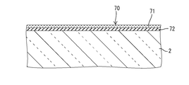
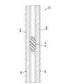
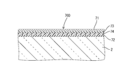
- FIG. 3 is a cross-sectional view of the corrosion liquid intrusion detection unit 70.
- the corrosion liquid intrusion detection unit 70 includes a base film 72 formed on the glass plate 2 and a metal film 71 formed on the base film 72.
- the base film 72 is made of the same material as the gate insulating film 26 described above, and is manufactured in the same manufacturing process as the gate insulating film 26.
- the metal film 71 is made of the same material as the pixel electrode (transparent electrode) 21 (that is, a transparent conductive film such as ITO) and is manufactured in the same manufacturing process as the pixel electrode 21.
- the corrosion liquid intrusion detection unit 70 is formed at a predetermined location using a pattern formation technique such as a photolithography technique.
- a pattern formation technique such as a photolithography technique.
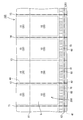
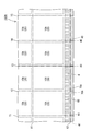
- FIG. 4 is a plan view of the liquid crystal panel assembly 100.
- the liquid crystal panel assembly 100 will be described with reference to FIG.
- each liquid crystal panel 10 is connected in an aligned state.
- a plurality of TFT array substrates 20 in each liquid crystal panel 10 are manufactured as a single large glass substrate (first mother glass substrate).
- This first mother glass substrate may be particularly referred to as a TFT array substrate assembly.
- each CF substrate 30 of each liquid crystal panel 10 is also manufactured as a single large glass substrate (second mother glass substrate).
- This second mother glass substrate may be particularly referred to as a CF substrate aggregate.
- Each liquid crystal panel 10 includes a plurality of planned dividing lines X1, X2, Y1, Y2, Y3, Y4 virtually set on the surface of the liquid crystal panel assembly 100 (that is, on the outer surface of the mother glass substrate). , Y5, respectively. As will be described later, scribe grooves are respectively formed along the planned dividing lines X1 and the like. 4 shows the liquid crystal panel aggregate 100 as viewed from the mother glass substrate 200 on the TFT array substrate 20 side. Similarly, for the mother glass substrate 300 on the CF substrate 20 side, a plurality of planned dividing lines are set.
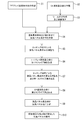
- FIG. 5 is a flowchart for explaining the procedure of the method for manufacturing the liquid crystal panel 10. As shown in FIG. 5, the liquid crystal panel 10 is manufactured through steps S1 to S10. Hereinafter, the manufacturing method of the liquid crystal panel 10 will be described separately for each step.
- Step S1 is a step of manufacturing a TFT array substrate assembly.
- a single-layer or multi-layer conductive film made of tungsten, titanium, aluminum, chromium, or the like is first formed on a large (large format) transparent glass plate (first mother glass plate).
- a known method such as a sputtering method can be applied.
- the conductive film provided on the plate is formed into a predetermined pattern using a photolithography technique or the like. In this way, the gate electrode line 22 and the gate electrode 22a having a predetermined pattern are obtained.
- the terminal pattern 60 is also formed at a predetermined position of the plate (first mother glass plate) by the same manufacturing process as the gate electrode line 22 and the like.
- a gate insulating film 26 is formed on the large glass plate on which the gate electrode lines 22 and the like are formed.
- the gate insulating film 26 is made of, for example, silicon nitride or the like, and is formed using a known method such as a plasma CVD method.
- a base film 72 of the corrosion liquid intrusion detection unit 70 is also formed.
- a semiconductor film 25, a source electrode line 23, a source electrode 23a, and a drain electrode 23b are formed on the gate insulating film 26, respectively.
- the semiconductor film 25 is made of, for example, n + type amorphous silicon or the like, and is formed using a known method such as a plasma CVD method.
- the source electrode line 23, the source electrode 23a, and the drain electrode 23b are formed using the same method as that for the gate electrode line 22 described above.
- an interlayer insulating film 27 made of a photosensitive resin is formed on the glass plate.
- an opening for forming the contact hole portion 21a is formed.
- the opening is formed using a photolithography technique or the like.
- a transparent conductive film made of ITO is formed on the surface of the interlayer insulating film 27 using a known method such as a sputtering method.
- the transparent conductive film is formed into a predetermined pattern using the photolithography technique or the like to become the pixel electrode 21. In this manner, the pixel electrode 21 having a predetermined pattern and the contact hole portion 21a are obtained.
- the metal film 71 of the corrosion liquid intrusion detection unit 70 is also formed.
- the metal film 71 is made of the same ITO as the pixel electrode 21.
- an alignment film 28 is formed so as to cover the pixel electrode 21 and the like.
- a liquid alignment film material made of polyimide or the like is applied using an apparatus such as a circular pressure printing apparatus or an ink jet printing apparatus. Thereafter, the applied alignment film material is dried, and the alignment film material is further irradiated with ultraviolet rays from a predetermined direction to perform an alignment process. Then, an alignment film 28 is formed on the pixel electrode 21.
- a TFT array substrate aggregate (first mother glass substrate) 200 in which a plurality of TFT array substrates 20 are connected in an aligned state is manufactured.
- columnar spacers are formed at predetermined positions of each TFT array substrate 20. By this spacer, the distance between the TFT array substrate 20 and the CF substrate 30 after being bonded to each other is kept constant.
- Step S2 is a step of producing a CF substrate assembly.
- a BM resist or the like is first applied on a large (large format) transparent glass plate (second mother glass plate).
- the BM resist is made of a photosensitive resin composition in which a black colorant is dispersed.
- the applied BM resist is formed into a predetermined pattern using a photolithography technique or the like. In this way, the BM 32 having a predetermined pattern is obtained on the plate (second mother glass plate).
- the colored light-sensitive material is composed of a photosensitive resin composition in which a colorant (pigment) of a predetermined color is dispersed.
- the applied colored light-sensitive material is formed into a predetermined pattern using a photolithography technique or the like. In this way, a CF layer (colored layer) 33 having a predetermined pattern is obtained.
- a transparent conductive film made of ITO is formed using a sputtering method or the like so as to cover the CF layer 33, the BM 32, and the like. This transparent conductive film becomes the common electrode 31.
- an alignment film 34 is formed so as to cover the common electrode 31.
- This alignment film 34 is formed by the same method as that formed on the TFT array substrate 20 (TFT array substrate assembly 200) side.
- step S2 a CF substrate aggregate (second mother glass substrate) 300 in which a plurality of CF substrates 30 are connected in an aligned state is manufactured.
- Step S3 is a step of forming a seal portion 40 on each CF substrate 30 of the CF substrate aggregate 300 and dropping a liquid crystal material.
- the seal part 40 is made of a thermosetting resin or a photocurable resin.
- the seal portion 40 is formed as a frame-like one that surrounds each alignment film 34 on the inner surface of each CF substrate 30 by using a screen printing apparatus or the like. Then, liquid crystal materials are dropped into the inside of the seal portion 40 formed in a frame shape by using an ink jet type discharge device or the like.
- Step S4 is a step of manufacturing the liquid crystal panel aggregate 100 by bonding the substrate aggregates 200 and 300 together.
- the TFT array substrate assembly 200 and the CF substrate assembly 300 on which the seal portion 40 and the like are formed are arranged to face each other in a vacuum chamber (not shown).
- substrate aggregates 200 and 300 are pressurized in the pressure_reduction
- the inside of the vacuum chamber is returned to the atmospheric pressure state
- the TFT array substrate assembly 200 and the CF substrate assembly 300 are constantly pressurized due to the difference between the atmospheric pressure and the internal pressure thereof.
- the seal portions 40 sandwiched between the two substrate assemblies 200 and 300 are cured.
- the liquid crystal panels 10 having a rectangular appearance are assigned in a state of being adjacent to each other.
- the seal portion 40 is formed as one large lattice pattern that surrounds the display area S of each liquid crystal panel 10. That is, the adjacent seal portions 40 are provided in a partially connected state.
- segmentation planned lines X1, Y1 etc. which were mentioned above are set so that it may pass through the approximate center of the part where the adjacent seal parts 40 were connected.
- each terminal pattern 60 provided on the inner surface of each TFT array substrate 20 is provided in a line.
- surroundings of each terminal pattern 60 may be provided along the parting planned lines X2, Y1, etc.
- the adjacent corrosive liquid intrusion detection units 70 are provided in a partially connected state. And it is set so that each parting planned line Y1, Y2, Y3, Y4, Y5 may pass on this connected part.
- the adjacent corrosive liquid intrusion detection units 70 and 70 are separated from each other.
- FIG. 4 there is a blank portion 201 that is not used as the liquid crystal panel 10 at the end of the TFT array substrate assembly 200.
- the CF board assembly is provided with a similar blank portion.
- the margin portion provided on the CF substrate assembly side is set larger than the margin portion 201.
- the margin portion 201 is a portion outside the planned dividing line X2 in the TFT array substrate assembly 200, and a linear shape that fills the gap between this portion and the margin portion on the CF substrate assembly side facing this portion.
- a spacer 41 is provided.
- the spacer 41 is made of the same material as the seal portion 40 and is manufactured in the same process. The spacer 41 prevents the etchant from entering from the end when the liquid crystal panel assembly 100 described later is thinned.
- Step S5 is a step (first thinning step) of thinning the liquid crystal panel aggregate 100 by an etching process.
- FIG. 6 is a cross-sectional view schematically showing the periphery of the seal portion 40 in the liquid crystal panel assembly 100 before being thinned.
- the thickness (plate thickness) of the TFT array substrate assembly 200 and the CF substrate assembly 300 is set to a final target plate thickness T (for example, 0.05 mm to 0.5 mm, preferably 0.1 mm).
- the thickness of the liquid crystal panel aggregate 100 is reduced by etching until it becomes the one that remains for ⁇ (for example, 50 ⁇ m to 100 ⁇ m) (that is, T + ⁇ ).
- FIG. 7 is a cross-sectional view of an etching tank used for thinning the liquid crystal panel assembly.
- the etching process is performed by immersing the liquid crystal panel aggregate 100 in an etching solution 81 filled in the etching tank 80.
- the liquid crystal panel aggregate 100 is accommodated in a dedicated tray 82 and immersed in the etching solution 81 while being accommodated in the tray 82.
- the etchant 81 a known one such as hydrofluoric acid is used.
- a large number of holes 82a are provided around the tray 81, and the etching solution 81 enters the inside of the tray 82 through the holes 82a. Then, the liquid crystal panel assembly 100 is thinned in the tray 81 using the etching solution 81 that has entered.
- an air supply pipe 83 connected to an air supply pump (not shown) is disposed below (bottom side) in the etching tank 80.
- the supply pipe 83 is provided with a large number of small holes 83a, and bubbles 84 are generated from the small holes 83a.
- the etching solution 81 is stirred by the bubbles 84 during the etching process.
- the bubble 84 is formed by ejecting a gas such as nitrogen gas supplied from the air supply pump from the small hole 83 a of the air supply pipe 83.
- both the thickness (plate thickness) of the TFT array substrate assembly 200 and the thickness (plate thickness) of the CF substrate assembly 300 gradually decrease (thin).
- the thickness of the TFT array substrate assembly 200 is gradually dissolved (etched) from the outer surface 200a side, and the thickness of the CF substrate assembly 300 is gradually dissolved from the outer surface 300a side. It becomes thin (etched).
- the liquid crystal panel assembly 100 is still accommodated in the tray 82 from the etching tank 80. After being taken out, the first etching process is completed. Then, the liquid crystal panel aggregate 100 is taken out from the tray 82.
- FIG. 8 is a cross-sectional view schematically showing the periphery of the seal portion 40 of the liquid crystal panel assembly 100 thinned by the first etching process (first thinning step).
- first thinning step the positions of the outer surfaces 200a and 300a in the substrate assemblies 200 and 300 before being etched (thinned) are indicated by chain lines.
- the thicknesses of the substrate assemblies 200 and 300 are reduced by the etching process.
- Step S6 is a step of forming a first scribe groove in the TFT array substrate assembly 200.
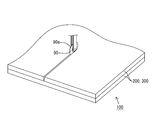
- FIG. 9 is a perspective view of a cutter wheel 90 used for forming a scribe groove.
- a scribe groove is formed on the outer surface of the liquid crystal panel assembly 100 after the etching process on the TFT array substrate assembly 200 side using a cutter wheel 90 as shown in FIG.
- the cutter wheel 90 includes a rotary blade 90a made of a single crystal of artificial diamond or the like. The outer peripheral side of the rotary blade 90a is tapered.
- FIG. 10 is a cross-sectional view schematically showing the periphery of the seal portion 40 of the liquid crystal panel assembly 100 in which the first scribe groove 200b is formed. As shown in FIG. 10, the first scribe groove 200 b is formed so as to be disposed substantially at the center with respect to a portion where adjacent seal portions 40, 40 are integrally formed. .
- Step S7 is a step (second thinning step) in which the liquid crystal panel assembly 100 is further thinned by etching and the first scribe groove 200b is grown.
- the remaining plate thickness ⁇ in the above-described step S5 (first thinning step) is removed by etching.
- assembly 200,300 is thinned so that it may become the plate
- Process S7 is performed by immersing the liquid crystal panel aggregate 100 in the etching solution 81 in the etching tank 80, as in the case of the process S5. Also in this case, as the etching process proceeds, both the thickness (plate thickness) of the TFT array substrate assembly 200 and the thickness (plate thickness) of the CF substrate assembly 300 gradually decrease (thin). The thickness of the TFT array substrate assembly 200 is gradually dissolved (etched) from the outer surface 200a side, and the thickness of the CF substrate assembly 300 is gradually dissolved from the outer surface 300a side. It becomes thin (etched).
- the liquid crystal panel aggregate 100 is removed from the etching tank 80.
- the second etching process is completed after the sheet is taken out while being accommodated in the tray 82. Thereafter, the liquid crystal panel aggregate 100 is appropriately removed from the tray 82.
- step S7 the first scribe groove 200b formed on the outer surface 200a of the TFT array substrate assembly 200 is also gradually etched.
- the first scribe groove 200b grows in the groove width direction and the groove depth direction.
- FIG. 11 is a cross-sectional view schematically showing the periphery of the seal portion 40 of the liquid crystal panel assembly 100 thinned by the second etching process.
- FIG. 11 shows the first scribe groove 200b grown by the etching process.
- the positions of the outer surfaces 200a and 300a in the respective substrate assemblies 200 and 300 before the second etching process are indicated by chain lines.
- the thickness of each of the substrate assemblies 200 and 300 is reduced by the etching process, and the first scribe groove 200b is enlarged.
- Step S8 is a step of forming the second scribe groove 300b in the CF substrate assembly 300.
- scribe grooves are formed on the outer surface of the liquid crystal panel assembly 100 after the second etching process on the CF substrate assembly 200 side, using the cutter wheel 90 (see FIG. 9).
- a plurality of planned dividing lines are also provided on the CF substrate assembly 300 side so as to partition each liquid crystal panel 10.
- the scribing groove 300b having a V-shaped cross section is formed in the CF substrate assembly 300 by rolling the rotating blade 90a of the cutter wheel 90 while pressing the rotating blade 90a on the outer surface 300a along the planned dividing line. Is done.
- FIG. 12 is a cross-sectional view schematically showing the periphery of the seal portion 40 of the liquid crystal panel assembly 100 in which the second scribe groove 300b is formed.
- the second scribe groove 300 b is formed so as to be disposed substantially at the center with respect to a portion where adjacent seal portions 40, 40 are integrally formed.
- channel 300b are mutually facing through the part in which the adjacent seal parts 40 and 40 are integrally formed.
- Step 9 is a step of dividing the liquid crystal panel aggregate 100 for each liquid crystal panel 10.
- a predetermined force is applied from the outside to the liquid crystal panel assembly 100 (see FIG. 12) in which the first scribe groove 200b and the second scribe groove 300b are formed.
- the first scribe groove 200b and the second scribe groove 300b are formed, and the portion where the thickness is thin (small) is divided.
- the portions where the adjacent seal portions 40 are integrally formed are separated from each other.
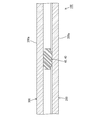
- FIG. 13 is a cross-sectional view schematically showing the liquid crystal panels 10 and 10 obtained by dividing the liquid crystal panel aggregate 100. As shown in FIG.
- the liquid crystal panel aggregate 100 is divided into individual liquid crystal panels 10 separated from each other at the first scribe groove 200 b and the second scribe groove 300 b. Note that the blank portion 201 and the like as shown in FIG. 4 included in the liquid crystal panel assembly 100 are also divided and removed in this step S9.
- the corrosion liquid intrusion detection units 70 and 70 in the adjacent liquid crystal panels 10 and 10 are also partially formed integrally as described above (see FIG. 4). Therefore, in step S9, the respective corrosive liquid intrusion detection units 70 and 70 are also separated and separated from each other.
- the corrosion liquid intrusion detection unit 70 finally formed in the liquid crystal panel 10 in this way is formed without a gap even at the outer edge portion of the TFT array substrate 20 and is suitable for detecting an etching liquid described later. .
- each liquid crystal panel 10 is divided in step S9, a plurality of liquid crystal panels 10 are obtained from the liquid crystal panel aggregate 100.
- the edge part (end surface) of each liquid crystal panel 10 is shape
- Step 10 is a step of removing the liquid crystal panel 10 in which the corrosion liquid intrusion detection unit 70 has changed color.
- the etching process is performed twice before the liquid crystal panel aggregate 100 is divided into the liquid crystal panels 10.
- the first scribe groove 200b is grown.
- a hole (through hole) penetrating the TFT array substrate assembly 200 is formed in some cases, for example, the bottom is removed.
- this hole is formed immediately above the seal portion 40, the hole is blocked by the seal portion 40, so that the etching solution enters the inside of the liquid crystal panel assembly 100 from the hole. Not to do.
- the etching liquid may enter the inside of the liquid crystal panel assembly 100 from the hole. is there.
- the etchant enters the inner surface side of the TFT array substrate assembly 200 and the etchant adheres to the terminal patterns 60 provided on each TFT array substrate 20, the terminal patterns 60 are corroded.
- the terminal pattern 60 is corroded, it causes a conduction failure and the liquid crystal panel 10 with the corroded terminal pattern 60 cannot be used as it is. Therefore, such a liquid crystal panel 10 needs to be distinguished from other liquid crystal panels in which the terminal pattern 60 is not corroded.
- each wiring constituting the terminal pattern 60 is very thin, when only a part thereof is corroded by the etching solution, the corrosion may be overlooked even if visual inspection is performed.
- each liquid crystal panel 10 of the present embodiment is provided with the corrosion liquid intrusion detection unit 70 as described above, the corrosion of the terminal pattern 60 can be easily found by visual inspection. The reason will be described below.
- the corrosion liquid intrusion detection unit 70 is disposed on the outer side (outer edge side) of the terminal pattern 60 on the inner surface of the TFT array substrate 20.
- the corrosion liquid intrusion detection unit 70 is disposed on the inner surface of the TFT array substrate 20 along the peripheral edge (outer edge) of the liquid crystal panel 10.
- the etching solution enters from the peripheral side of the liquid crystal panel 10, and therefore, when the terminal pattern 60 is corroded by the etching solution, it passes through the corrosion solution intrusion detection unit 70 located outside the terminal pattern 60. It will be.
- the corrosion liquid intrusion detection unit 70 includes a metal film on the uppermost layer (outermost layer) (see FIG. 3).
- the metal film is made of transparent ITO. When this metal film comes into contact with the etching solution (corrosion solution), it reacts with the etching solution to change (discolor) the color of the metal film.
- the corrosion liquid intrusion detection unit 70 when the corrosion liquid intrusion detection unit 70 is discolored, there is a possibility that the etching liquid has reached the terminal pattern 60 on the inner side, and the terminal pattern 60 is corroded. I can guess. In this way, the corrosion of the terminal pattern 60 can be determined by the change in the color of the corrosion liquid intrusion detection unit 70.
- the corrosion liquid intrusion detection unit 70 has a base film 72 below the metal film 71, so that the light transmittance (transparency) is somewhat suppressed. It is easy.
- the corroded liquid crystal panel 10 of the terminal pattern 60 can be easily found from the plurality of liquid crystal panels 10 by visual inspection.
- the discoloration of the corrosion liquid intrusion detection unit 70 may be confirmed directly with the naked eye, or may be confirmed using a device such as a loupe or a CCD camera.
- step S9 the liquid crystal panel 10 in which the corrosion liquid intrusion detection unit 70 has been discolored can be easily excluded from the other liquid crystal panels 10.
- the base film 72 of the corrosion liquid intrusion detection unit 70 also improves the adhesion of the metal film 71 to the plate 2.
- the liquid crystal panel 10 in which the terminal pattern 60 is corroded by the etching solution can be easily found. Therefore, according to the liquid crystal panel manufacturing method of the present embodiment, it is possible to efficiently manufacture the liquid crystal panel 10 made of only non-defective products while excluding the liquid crystal panel 10 in which the terminal pattern 60 is corroded by the etching solution.
- the corrosion liquid intrusion detection unit 70 provided in the liquid crystal panel 10 of the present embodiment can be manufactured using an existing manufacturing process. Therefore, the liquid crystal panel 10 according to the present embodiment does not require a new manufacturing process to be manufactured substantially in order to manufacture the corrosion liquid intrusion detection unit 70, and the manufacturing cost for adding the corrosion liquid intrusion detection unit 70 is low. It can be suppressed.
- the etching solution intrusion path includes not only the holes formed in the TFT array substrate assembly 200 but also the holes formed on the CF substrate assembly 300 side and the gaps at the ends of the liquid crystal panel assembly 100 (that is, Or a gap between the substrate assemblies 200 and 300).
- FIG. 14 is a plan view of the liquid crystal panel 10A of the second embodiment
- FIG. 15 is a plan view of the liquid crystal panel aggregate 100A of the second embodiment.
- the liquid crystal panel aggregate 100A shown in FIG. 15 is shown as viewed from the TFT array substrate aggregate 200 side, as in the first embodiment shown in FIG.
- the basic configuration of the liquid crystal panel 10A and the liquid crystal panel aggregate 100A of the present embodiment and the manufacturing method thereof are the same as those in the first embodiment.
- the shape (pattern) of the corrosion liquid intrusion detection unit 70A provided in the liquid crystal panel 10A is different from that of the first embodiment.
- the differences will be mainly described.
- the corrosion liquid intrusion detection unit 70 ⁇ / b> A is disposed outside the terminal pattern 60 on the inner surface of the TFT array substrate 20 as in the first embodiment.
- the corrosion liquid intrusion detection unit 70 ⁇ / b> A of the present embodiment is provided in a portion inside the outer edge of the TFT array substrate 20.
- each corrosive-solution intrusion detection part 70A in each adjacent liquid crystal panel 10A is previously formed in the TFT array board
- the corrosion liquid intrusion detection unit 70 ⁇ / b> A may be formed at least in a portion outside the terminal pattern 60, and may not necessarily be formed to fill up the outer edge portion of the TFT array substrate 20.
- FIG. 16 is a partially enlarged plan view of the corrosion liquid intrusion detection unit 70B formed in the liquid crystal panel 10B of the third embodiment.
- the basic configuration and manufacturing method of the liquid crystal panel 10B of the present embodiment are the same as those of the first embodiment.
- the liquid crystal panel 10B of the present embodiment is different from that of the first embodiment in the shape (pattern) of the corrosion liquid intrusion detection unit 10B formed on the inner surface of the TFT array substrate 20.
- the differences will be mainly described.
- the corrosion liquid intrusion detection unit 70 ⁇ / b> B is arranged outside the terminal pattern 60 on the inner surface of the TFT array substrate 20 as in the first embodiment.
- the corrosion liquid intrusion detection unit 70 ⁇ / b> B is formed in a state of being divided into a plurality at locations along the outer edge of the TFT array substrate 20. That is, the corrosion liquid intrusion detection unit 70B of the present embodiment is not a continuous shape as in the first embodiment, but has a shape that is partially interrupted.
- the corrosion liquid intrusion detection unit 70B provided in the liquid crystal panel 10B does not always need to be continuously formed, and may have a shape that is partially interrupted.
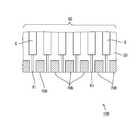
- a marker 61 is provided on the front side of each wiring 6 constituting the terminal pattern 60.
- the marker 61 is formed thinner than the wiring 6.
- FIG. 17 is a partial enlarged cross-sectional view of the corrosive liquid intrusion detection unit 70C formed in the liquid crystal panel of the fourth embodiment.
- the basic configuration and manufacturing method of the liquid crystal panel of the present embodiment are the same as those of the first embodiment.
- the configuration of the corrosion liquid intrusion detection unit 70C is different from that of the first embodiment.
- the differences will be mainly described.
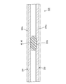
- the corrosion liquid intrusion detection unit 70C includes a metal film 71 on the uppermost layer (outermost layer) as in the first embodiment.
- a base film 72 is formed on the glass plate 2.
- the corrosion liquid intrusion detection unit 70C of the present embodiment includes an intermediate film 73 between them.
- the intermediate film 73 is made of the same material as that of the source electrode line 23 (see FIG. 1) and is manufactured in the same manufacturing process.
- the intermediate film 73 is formed so as to be sandwiched between the metal film 71 and the base film 72, the light transmittance (transparency) is suppressed by the intermediate film 73. It becomes easy to determine the color change of the portion 70C.
- FIG. 18 is a partial enlarged cross-sectional view of a corrosive liquid intrusion detection unit 70D formed on the liquid crystal panel of the fifth embodiment.
- the basic configuration and manufacturing method of the liquid crystal panel of the present embodiment are the same as those of the first embodiment.
- the configuration of the corrosion liquid intrusion detection unit 70D is different from that of the first embodiment.
- the differences will be mainly described.
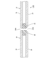
- the corrosion liquid intrusion detection unit 70D includes a metal film 71 on the uppermost layer (outermost layer) as in the first embodiment.
- a base film 72 is formed on the glass plate 2.
- the corrosion liquid intrusion detection unit 70D of the present embodiment includes two (two layers) intermediate films 73 and 74 between them.
- the intermediate film 73 is disposed on the upper side, and the intermediate film 74 is disposed on the lower side.
- the intermediate film 73 is made of the same material as the source electrode line 23 (see FIG. 1) and is manufactured in the same manufacturing process.
- the intermediate film 74 is made of the same material as the gate electrode line 74 (see FIG. 1) and is manufactured in the same manufacturing process.
- the two intermediate films 73 and 74 are formed so as to be sandwiched between the metal film 71 and the base film 72, the light transmittance (transparency) is suppressed by the intermediate films 73 and 74. Therefore, the discoloration of the corrosion liquid intrusion detection unit 70D can be easily determined.
- the metal film in the corrosion liquid intrusion detection unit is formed on the glass plate through the base film.
- the metal film is formed directly on the glass plate. It may be formed.
- the corrosion liquid intrusion detection unit is finally in a state where it is formed on the liquid crystal panel.
- the corrosion liquid intrusion detection unit is a TFT array substrate. It is good also as a structure which can finally peel from.
- the liquid crystal panels in the liquid crystal panel assembly are continuously connected to each other without a gap (for example, see FIG. 4).
- the liquid crystal panels may be connected to each other via a blank portion.
- the seal portions in the adjacent liquid crystal panels may be already separated from each other in the state of the liquid crystal panel aggregate, or the line width is increased in advance so that a part remains in the blank portion after the division.
- each seal portion may be formed.
- the corrosion liquid intrusion detection unit is provided with a metal film.
- the liquid other than the metal film whose color changes when it comes into contact with the etching liquid is entered. You may use as a detection part.
- the second scribe groove is formed in the CF substrate assembly through the second thinning process (second etching process). After that, the panel aggregate is divided for each liquid crystal panel.
- a scribe groove is first formed in the CF substrate aggregate, and then the TFT array is subjected to a second thinning step.
- a scribe groove may be formed in the substrate assembly, and then the panel assembly may be divided for each liquid crystal panel. That is, in other embodiments, the second scribe groove may be formed before the first scribe groove.
- a scribe groove is formed in each of the TFT array substrate assembly and the CF substrate assembly, and then a second thinning process is performed for each liquid crystal panel. It may be divided. That is, in another embodiment, both the first scribe groove and the second scribe groove may be formed in each substrate aggregate before the second thinning step.
- DESCRIPTION OF SYMBOLS 10 ... Liquid crystal panel, 2 ... Glass plate, 20 ... TFT array substrate (glass substrate), 21 ... Pixel electrode (transparent electrode), 21a ... Contact hole part, 22 ... Gate electrode line, 23 ... Source electrode line, 23a ... Source Electrode, 23b ... Drain electrode, 24 ... TFT, 25 ... Semiconductor film, 26 ... Gate insulating film (insulating film), 27 ... Interlayer insulating film, 28 ... Alignment film, 30 ... CF substrate, 3 ... Glass plate, 31 ... Common Electrode, 32 ... BM, 33 ... CF layer, 34 ... alignment film, 40 ... sealing part, 50 ... liquid crystal layer, 60 ... terminal pattern, 70 ... corrosion liquid intrusion detection part, 100 ... liquid crystal panel assembly, 200 ... TFT array Substrate assembly (mother glass substrate), 300 ... CF substrate assembly (mother glass substrate)
Landscapes
- Physics & Mathematics (AREA)
- Nonlinear Science (AREA)
- Mathematical Physics (AREA)
- Chemical & Material Sciences (AREA)
- Crystallography & Structural Chemistry (AREA)
- General Physics & Mathematics (AREA)
- Optics & Photonics (AREA)
- Liquid Crystal (AREA)
Abstract
本発明に係る液晶パネル10は、液晶層50と、この液晶層50の回りを囲むシール部40と、液晶層50及びシール部40を挟んで互いに向かい合う一対のガラス基板20,30と、一方のガラス基板20の内面上においてシール部40よりも外側に配される端子パターン60と、前記内面上において端子パターン60よりも外側に配されると共に、腐蝕液と接触すると変色する腐蝕液浸入検出部70とを備え、このような腐蝕液浸入検出部の変色によって、端子パターンの腐蝕を判別可能となる。
Description
本発明は、液晶パネル、液晶パネル集合体、及び液晶パネルの製造方法に関する。
近年、コンピュータ、テレビ等の家電製品の表示部として、液晶パネルが広く用いられている。液晶パネルは、一般には、薄膜トランジスタ(以下、TFT)アレイ基板とカラーフィルタ(以下、CF)基板とからなる一対の基板が、所定の間隔を置いて平行に対向して貼り合わせられ、両基板間に液晶が封止された構成をなしている。
通常、TFTアレイ基板には複数のTFTやこれに接続された画素電極がマトリクス状に形成され、CF基板にはCFがマトリクス状に形成されると共にその全面に共通電極が形成されており、これら電極間に印加する電圧を変化させることで、液晶を配向制御することができるようになっている。
このような液晶パネルを製造するにあたっては、大きなマザー基板(液晶パネル複数枚取り用の大型のガラス基板)に対して複数の液晶パネル分の画素電極やCFをそれぞれ形成する等、製造工程の途中までは、マザー基板のままで処理が行われている。
そして、携帯電話やデジタルカメラ等に用いられる小型の液晶パネルでは、マザー基板同士を貼り合せて大判(大型)パネルとした後に個々に分割することが行われている。
特に近年では、小型の前記液晶パネルに関しては、軽量化や大画面化を行うべく、薄型化及び狭額縁化が要望されている。この場合の薄型化とは、液晶パネルを構成する基板、具体的には上述したような画素電極等が形成されたTFTアレイ基板及びCF等が形成されたCF基板の薄板化である。また、狭額縁化とは、液晶パネルの表示領域における面積の拡大化、つまり表示領域を囲むパネル額縁領域の面積の縮小化である。
特許文献1には、薄型化に関する技術が開示されている。具体的には、TFTアレイ基板集合体と、CF基板集合体を、各表示領域を囲むように形成されたシール部を介して互いに貼り合わせ、両基板集合体間の複数の表示領域にそれぞれ液晶層を設けてパネル集合体(大判パネル)を作製する。
次いで、フッ酸等からなるエッチング液を用いてパネル集合体をエッチング処理することにより、各基板集合体をそれぞれ薄板化する。このようなエッチング処理においては、エッチング槽に貯留されているエッチング液中にパネル集合体を浸漬する工程が行われる。
その後、各基板集合体を、回転刃を有するカッターホイール等を用いてスクライブ溝を形成し、そのスクライブ溝に沿ってパネル集合体を分割すると、複数枚の液晶パネルが得られることになる。
これによれば、パネル集合体の状態で各基板集合体をそれぞれ薄板化することができるので、例えば、分割した後に液晶パネルを薄板化する場合と比べて、製造効率が高いという利点がある。
ただし、薄型化された状態のパネル集合体を分割するのは、薄型化されていない状態のパネル集合体を分割する場合と比べて、所定のパネル外径寸法となるように精度良く分割することが困難な場合がある。
特許文献2には、薄型化された状態のパネル集合体を精度良く分割し、液晶パネルの薄型化を行う技術が示されている。
(発明が解決しようとする課題)
しかしながら、スクライブ溝が形成された大判(大型)パネルに対してケミカルエッチングを行う際に、スクライブ溝が成長し過ぎる等して、マザー基板に貫通孔が形成されることがある。このような孔が形成されると、その孔から前記マザー基板の内面側にまでエッチング液が浸入し、TFTアレイ基板内面上に形成されている端子パターンを腐蝕させてしまうことがあり、問題となっている。
しかしながら、スクライブ溝が形成された大判(大型)パネルに対してケミカルエッチングを行う際に、スクライブ溝が成長し過ぎる等して、マザー基板に貫通孔が形成されることがある。このような孔が形成されると、その孔から前記マザー基板の内面側にまでエッチング液が浸入し、TFTアレイ基板内面上に形成されている端子パターンを腐蝕させてしまうことがあり、問題となっている。
端子パターンが腐蝕すると導通不良等が生じるため、その腐蝕した端子パターンが形成されている部分の液晶パネルは、使用できなくなる。なお、前記端子パターンは、通常、複数本の細かな配線が集まったものからなるため、その一部分のみがエッチング液によって腐蝕していても、その腐蝕部分を視覚的に検出(判別)することが難しい場合があり、問題となっている。
本発明の目的は、液晶パネルを構成する基板をケミカルエッチングによって薄板化する場合に、エッチング液(腐蝕液)によって腐蝕されている端子パターンを備えた液晶パネルを容易に判別できる技術を提供することである。
(課題を解決するための手段)
本発明に係る液晶パネルは、液晶層と、この液晶層の回りを囲むシール部と、前記液晶層及び前記シール部を挟んで互いに向かい合う一対のガラス基板と、一方の前記ガラス基板の内面上において前記シール部よりも外側に配される端子パターンと、前記内面上において前記端子パターンよりも外側に配されると共に、腐蝕液と接触すると変色する腐蝕液浸入検出部と、を備える。前記液晶パネルは、腐蝕液浸入検出部の変色によって、端子パターンの腐蝕を判別できる。
本発明に係る液晶パネルは、液晶層と、この液晶層の回りを囲むシール部と、前記液晶層及び前記シール部を挟んで互いに向かい合う一対のガラス基板と、一方の前記ガラス基板の内面上において前記シール部よりも外側に配される端子パターンと、前記内面上において前記端子パターンよりも外側に配されると共に、腐蝕液と接触すると変色する腐蝕液浸入検出部と、を備える。前記液晶パネルは、腐蝕液浸入検出部の変色によって、端子パターンの腐蝕を判別できる。
前記液晶パネルにおいて、前記腐蝕液浸入検出部が、金属膜を含んでもよい。
前記液晶パネルにおいて、前記腐蝕液浸入検出部が、金属膜と、この金属膜の下側に敷かれる下地膜とを含んでもよい。前記液晶パネルは、金属膜の下側に下地膜を備えているため、腐蝕液浸入検出部の変色の有無が判別し易い。
前記液晶パネルにおいて、前記腐蝕液浸入検出部が、金属膜と、下地膜と、これらの間で挟まれる1つ又は2つ以上の中間膜とを含んでもよい。前記液晶パネルは、金属膜と、下地膜と、これらの間で挟まれる1つ又は2つ以上の中間膜とを含んでいるため、腐蝕液浸入検出部の変色の有無が判別し易い。
前記液晶パネルにおいて、前記金属膜が、一方の前記ガラス基板の内面上に配されている透明電極と同じ材料からなると共に、前記透明電極と同じ形成工程で形成されてもよい。前記液晶パネルは、その金属膜が透明電極と同じ形成工程で形成されるため、製造効率が良い。
前記液晶パネルにおいて、前記下地膜が、一方の前記ガラス基板の内面上に配されている絶縁膜と同じ材料からなると共に、前記絶縁膜と同じ形成工程で形成されてもよい。前記液晶パネルは、その下地膜が絶縁膜と同じ形成工程で形成されるため、製造効率が良い。
前記液晶パネルにおいて、前記中間膜が、一方の前記ガラス基板の内面上に配されているゲート電極又はソース電極と同じ材料からなると共に、前記ゲート電極又はソース電極と同じ形成工程で形成されてもよい。前記液晶パネルは、その中間膜がゲート電極又はソース電極と同じ形成工程で形成されるため、製造効率が良い。
前記液晶パネルにおいて、前記腐蝕液浸入検出部が、前記端子パターンの回りを、前記シール部と共に取り囲んでもよい。前記液晶パネルは、腐蝕液浸入検出部が、端子パターンの回りをシール部と共に取り囲んでいるため、エッチング液の浸入を確実に検出できる。
また、本発明に係る液晶パネル集合体は、前記液晶パネルを、複数個まとめて製造するための液晶パネル集合体であって、一方のガラス基板同士が、互いに繋がってなる一方のマザーガラス基板と、他方のガラス基板同士が、互いに繋がってなる他方のマザーガラス基板と、前記マザーガラス基板間で挟まれる複数の液晶層と、前記マザーガラス基板間で挟まれる複数のシール部と、一方のマザーガラス基板の内面上に配される複数の端子パターンと、一方のマザーガラス基板の内面上に配される複数の腐蝕液浸入検出部と、を備える。
また、本発明に係る液晶パネルの製造方法は、前記液晶パネル集合体を、液晶パネル毎に分断するために、少なくとも一方のマザーガラス基板の外面上にスクライブ溝を形成する工程と、前記スクライブ溝に腐蝕液を接触させて、前記スクライブ溝を成長させる工程と、成長後の前記スクライブ溝に沿って、前記液晶パネル集合体が液晶パネル毎に分断される工程と、分断された各液晶パネルの中から、腐蝕液浸入検出部が前記腐蝕液によって変色したものを除外する工程と、を備える。
(発明の効果)
本発明によれば、液晶パネルを構成する基板をケミカルエッチングによって薄板化する場合に、エッチング液(腐蝕液)によって腐蝕されている端子パターンを備えた液晶パネルを容易に判別できる技術を提供できる。
本発明によれば、液晶パネルを構成する基板をケミカルエッチングによって薄板化する場合に、エッチング液(腐蝕液)によって腐蝕されている端子パターンを備えた液晶パネルを容易に判別できる技術を提供できる。
<実施形態1>
本発明の一実施形態に係る液晶パネルの製造方法、この製造方法で利用される液晶パネル集合体、及びこの製造方法で得られる液晶パネルについて、図1ないし図13を参照しつつ説明する。先ず図1及び図2を参照しつつ、本実施形態の液晶パネルの構成を説明する。
本発明の一実施形態に係る液晶パネルの製造方法、この製造方法で利用される液晶パネル集合体、及びこの製造方法で得られる液晶パネルについて、図1ないし図13を参照しつつ説明する。先ず図1及び図2を参照しつつ、本実施形態の液晶パネルの構成を説明する。
(液晶パネル)
図1は、液晶パネル10の断面図である。図1に示されるように、液晶パネル10は、主として、TFTアレイ基板(ガラス基板の一例)20、CF基板(ガラス基板の一例)30、シール部40、液晶層50等を備えている。
図1は、液晶パネル10の断面図である。図1に示されるように、液晶パネル10は、主として、TFTアレイ基板(ガラス基板の一例)20、CF基板(ガラス基板の一例)30、シール部40、液晶層50等を備えている。
TFTアレイ基板20は、透明なガラス製の板2上に、複数の画素電極(透明電極)21がマトリクス状に形成されている。各画素電極21の周囲には、走査電極線であるゲート電極線22と、画像信号電極線であるソース電極線23とが互いに交差するように形成されている。
ゲート電極線22とソース電極線23とは、それらの交差部において、ソース電極線23がゲート電極配線22の上側となるようにそれぞれ配されている。その交差部において、ゲート電極線22とソース電極線23とは、ゲート絶縁膜26を介して互いに電気的に絶縁されている。また、ゲート電極線22とソース電極線23との交差部には、スイッチング素子としてのTFT24が形成されている。TFT24は、ゲート電極線22の一部であるゲート電極22aに接続されている。
TFT24が形成されている領域のゲート絶縁膜26の上側には、半導体膜25が、ゲート電極22aに対して重畳するように形成されている。また、その半導体膜25の上側には、ソース電極線23の一部であるソース電極23aと、ドレイン電極23bとがそれぞれ形成されている。なお、ソース電極23aとドレイン電極23bとは、ゲート電極22aを挟んで互いに間隔を保った状態で、半導体膜25上に形成されている。そして、ドレイン電極23bが画素電極21のコンタクトホール部21aを介して画素電極21に接続されている。
TFT24は、ゲート電極線22のゲート電極22aより供給される走査信号電圧によって、オン・オフが切り替えられる。また、ソース電極線23のソース電極23bより供給される画像信号電圧は、オン状態のTFT24によってドレイン電極23b及びコンタクトホール部21aを介して画素電極21に供給される。
このようなTFT24は、ゲート絶縁膜26の上側に形成されている層間絶縁膜27によって覆われている。なお、この層間絶縁膜27上には、画素電極21が形成されている。画素電極21は、例えば、ITO(Indium Tin Oxide)等の透明導電膜により形成されている。この画素電極21の上側には、紫外線等を利用した配向処理が施されているポリイミド膜等からなる配向膜28が形成されている。液晶層50中に含まれている液晶物質は、この配向膜28によって配向規制される。
CF基板30は、TFTアレイ基板20と対向するように配されており、TFTアレイ基板20との間で液晶層50を挟んでいる。CF基板30は、透明なガラス製の板3上に、上述したゲート電極線22及びソース電極線23が形成された領域を遮光するように格子状のブラックマトリクス(以下、BM)32が形成されている。BM32で囲まれた領域には、赤、青、緑等のCF層(着色層)33が形成されている。
そして、CF層33及びBM32の表面を覆うように、TFTアレイ基板20の各画素電極21と対向する共通電極31が形成されている。図1において、共通電極31は、CF層33及びBM32の下側に示されている。この共通電極31も、画素電極21と同様、ITO等の透明導電膜によって形成されている。また、共通電極31の表面を覆うように、配向膜34が形成されている。この配向膜34も、TFTアレイ基板20側のものと同様、紫外線等を利用した配向処理が施されているポリイミド膜等からなり、液晶層50中に含まれている液晶物質の配向規制を行っている。
なお、このような両基板20,30によって挟まれている液晶層50は、シール部40によって封止されている。図1に示されるように、このシール部40も、両基板20,30によって挟まれている。図2は、液晶パネル10の平面図である。図2に示されるように、液晶層50の周りを囲む枠状のシール部40が形成されている。なお、図2には、CF基板30側から見た液晶パネル10が示されている。
図2に示されるように、TFTアレイ基板20、及びCF基板30は、共に矩形状(四角形状)である。ただし、図2において下側に配されているTFTアレイ基板20の方が、上側に配されているCF基板30よりも大きい。TFTアレイ基板20とCF基板30とは、それぞれ短辺側における一方の端部の位置がそろえられている。そして、短辺側における他方の端部の位置は異なっており、TFTアレイ基板30の一部が、CF基板20よりも外側にはみ出している。このはみ出した部分におけるTFTアレイ基板30の内面上には、端子パターン60が形成されている。この端子パターン60は、複数本の細かな配線からなり、アルミニウム等の金属材料からなる。なお、この端子パターン60上には、図示されない液晶パネル10を駆動させるためのドライバICが実装されている。
端子パターン60は、シール部40よりも外側におけるTFTアレイ基板20の内面上に形成されている。本実施形態の場合、端子パターン60は、ガラス製の板2上に形成されており、その一部は、CF基板30の短辺側における端部によって覆われている。この端子パターン60をなす各配線6の一端は、上述したソース電極配線22、ゲート電極配線23等に接続されている。これに対して、それらの他端は、図示されないフレキシブルプリント基板(FPC)の端子部と、異方性導電フィルム(ACF)を介して接続される。なお、端子パターン60は、TFTアレイ基板20の周縁までは形成されておらず、周縁よりも内側の部分に配されている。
また、端子パターン60よりも外側におけるTFTアレイ基板20の内面上には、腐蝕液浸入検出部70が形成されている。図2に示されるように、腐蝕液浸入検出部70は、端子パターン60を囲むように、TFTアレイ基板20の周縁に沿って設けられている。腐蝕液浸入検出部70は、連続した一本の帯状(線状)であり、その幅は、端子パターン70を構成する各配線6よりも大きく設定されている。本実施形態の場合、その幅は、シール部40の幅よりも若干細く設定されている。なお、端子パターン60は、TFTアレイ基板20の内面上において、シール部40と、腐蝕液浸入検出部70とによって取り囲まれている。
図3は、腐蝕液浸入検出部70の断面図である。図3に示されるように、腐蝕液浸入検出部70は、ガラス製の板2上に形成されている下地膜72と、この下地膜72上に形成されている金属膜71とからなる。下地膜72は、上述したゲート絶縁膜26と同じ材料からなると共に、そのゲート絶縁膜26と同じ製造工程で製造される。そして、金属膜71は、上述した画素電極(透明電極)21と同じ材料(つまり、ITO等の透明導電膜)からなると共に、その画素電極21と同じ製造工程で製造される。
腐蝕液浸入検出部70は、フォトリソグラフィ技術等のパターン形成技術を利用して、所定の場所に形成される。腐蝕液浸入検出部70は、フッ酸等からなるエッチング液(腐蝕液)と接触すると、エッチング液と反応して、変色する。
(液晶パネル集合体)
本実施形態の液晶パネル10は、1つの大型パネルの状態で、複数個まとめて製造される。図4は、液晶パネル集合体100の平面図である。ここで、液晶パネル集合体100について図4等を参照しつつ説明する。
本実施形態の液晶パネル10は、1つの大型パネルの状態で、複数個まとめて製造される。図4は、液晶パネル集合体100の平面図である。ここで、液晶パネル集合体100について図4等を参照しつつ説明する。
図4に示されるように、大型パネルとしての液晶パネル集合体100中では、複数個の液晶パネル10は、互いに配列された状態で繋がっている。各液晶パネル10における各TFTアレイ基板20は、複数個まとめて一枚の大型のガラス基板(第1マザーガラス基板)として製造される。この第1マザーガラス基板のことを、特に、TFTアレイ基板集合体と称する場合がある。また、各液晶パネル10の各CF基板30も、複数個まとめて一枚の大型のガラス基板(第2マザーガラス基板)として製造される。この第2マザーガラス基板のことを、特に、CF基板集合体と称する場合がある。これらのマザーガラス基板が、後述するように液晶層50及びシール部40等を挟んだ状態で互いに貼り合せられると、図4に示されるような、液晶パネル集合体1となる。
各液晶パネル10は、液晶パネル集合体100の表面上(つまり、マザーガラス基板の外表面上)に仮想的に設定されている複数本の分断予定線X1,X2,Y1,Y2,Y3,Y4,Y5によって、それぞれ区画されている。後述するように、これらの分断予定線X1等に沿ってスクライブ溝がそれぞれ形成される。なお、図4には、TFTアレイ基板20側のマザーガラス基板200から見た液晶パネル集合体100が示されている。CF基板20側のマザーガラス基板300についても、同様に、複数本の分断予定線が設定されている。
(液晶パネルの製造方法)
図5は、液晶パネル10の製造方法の手順を説明するフローチャートである。図5に示されるように、液晶パネル10は、工程S1ないし工程S10を経て製造される。以下、液晶パネル10の製造方法を、各工程に分けて説明する。
図5は、液晶パネル10の製造方法の手順を説明するフローチャートである。図5に示されるように、液晶パネル10は、工程S1ないし工程S10を経て製造される。以下、液晶パネル10の製造方法を、各工程に分けて説明する。
(工程S1)
工程S1は、TFTアレイ基板集合体を作製する工程である。この工程S1では、先ず、大型(大判)の透明なガラス製の板(第1マザーガラス板)上に、タングステン、チタン、アルミニウム、クロム等からなる単層又は多層の導電膜が形成される。この導電膜を形成する方法としては、スパッタリング法等の公知の手法を適用できる。そして、前記板上に設けられた導電膜は、フォトリソグラフィ技術等を利用して、所定のパターンに成形される。このうようにして、所定のパターンを成すゲート電極線22及びゲート電極22aが得られる。なお、端子パターン60も、ゲート電極線22等と同じ製造工程によって、前記板(第1マザーガラス板)の所定個所に形成される。
工程S1は、TFTアレイ基板集合体を作製する工程である。この工程S1では、先ず、大型(大判)の透明なガラス製の板(第1マザーガラス板)上に、タングステン、チタン、アルミニウム、クロム等からなる単層又は多層の導電膜が形成される。この導電膜を形成する方法としては、スパッタリング法等の公知の手法を適用できる。そして、前記板上に設けられた導電膜は、フォトリソグラフィ技術等を利用して、所定のパターンに成形される。このうようにして、所定のパターンを成すゲート電極線22及びゲート電極22aが得られる。なお、端子パターン60も、ゲート電極線22等と同じ製造工程によって、前記板(第1マザーガラス板)の所定個所に形成される。
次いで、ゲート電極線22等が形成された大型の前記ガラス板上に、ゲート絶縁膜26が形成される。このゲート絶縁膜26は、例えば、窒化シリコン等からなり、プラズマCVD法等の公知の手法を用いて形成される。なお、このゲート絶縁膜26の形成時に、腐蝕液浸入検出部70の下地膜72も形成される。そしてこのゲート絶縁膜26上に、半導体膜25、ソース電極線23、ソース電極23a、ドレイン電極23bがそれぞれ形成される。半導体膜25は、例えば、n+型のアモルファスシリコン等からなり、プラズマCVD法等の公知の手法を用いて形成される。そして、ソース電極線23、ソース電極23a、ドレイン電極23bは、上述したゲート電極線22と同様の手法を用いてそれぞれ形成される。
次いで、感光性樹脂からなる層間絶縁膜27が前記ガラス板上に形成される。この層間絶縁膜27には、コンタクトホール部21aを形成するための開口部が形成される。この開口部は、フォトリソグラフィ技術等を利用して形成される。そして、この層間絶縁膜27の表面上には、ITOからなる透明導電膜が、スパッタリング法等の公知の手法を用いて形成される。その後、この透明導電膜は、フォトリソグラフィ技術等を利用して、所定のパターンに成形されて画素電極21となる。このようにして、所定のパターンの画素電極21及びそのコンタクトホール部21aが得られる。なお、この画素電極21の形成時に、腐蝕液浸入検出部70の金属膜71も形成される。この金属膜71は、画素電極21と同じITOからなる。
画素電極21が形成された後、その画素電極21等を覆うように、配向膜28が形成される。円圧式印刷装置、インクジェット式印刷装置等の装置を用いて、ポリイミド等からなる液状の配向膜原料が塗布される。その後、塗布された配向膜原料を乾燥させ、更に、その配向膜原料に対して所定の方向から紫外線を照射して配向処理を行う。すると、画素電極21上に、配向膜28が形成される。
以上のようにして、工程S1において、複数個のTFTアレイ基板20が互いに配列された状態で繋がったTFTアレイ基板集合体(第1マザーガラス基板)200が作製される。なお、各TFTアレイ基板20の所定個所には、図示されない柱状のスペーサーが形成されている。このスペーサーによって、互いに貼り合わせられた後のTFTアレイ基板20と、CF基板30との間隔が一定に保たれる。
(工程S2)
工程S2は、CF基板集合体を作製する工程である。この工程S2では、先ず、大型(大判)の透明なガラス製の板(第2マザーガラス板)上に、BMレジスト等が塗布される。BMレジストは、黒色着色剤を分散させた感光性樹脂組成物等からなる。次いで、塗布されたBMレジストを、フォトリソグラフィ技術等を利用して、所定のパターンに成形する。このようにして、前記板(第2マザーガラス板)上に、所定のパターンを成すBM32が得られる。
工程S2は、CF基板集合体を作製する工程である。この工程S2では、先ず、大型(大判)の透明なガラス製の板(第2マザーガラス板)上に、BMレジスト等が塗布される。BMレジストは、黒色着色剤を分散させた感光性樹脂組成物等からなる。次いで、塗布されたBMレジストを、フォトリソグラフィ技術等を利用して、所定のパターンに成形する。このようにして、前記板(第2マザーガラス板)上に、所定のパターンを成すBM32が得られる。
次いで、赤色、緑色、青色等の各色の着色感材が、前記板上に塗布される。着色感材は、所定の色の着色剤(顔料)を分散させた感光性樹脂組成物等からなる。塗布された着色感材は、フォトリソグラフィ技術等を利用して、所定のパターンに成形される。このようにして、所定のパターンを成すCF層(着色層)33が得られる。次いで、CF層33及びBM32等を覆うように、ITOからなる透明導電膜が、スパッタリング法等を利用して形成される。そして、この透明導電膜が共通電極31となる。
次いで、共通電極31を覆うように配向膜34が形成される。この配向膜34は、TFTアレイ基板20(TFTアレイ基板集合体200)側に形成されるものと同様の手法により形成される。
以上のようにして、工程S2において、複数個のCF基板30が互いに配列された状態で繋がったCF基板集合体(第2マザーガラス基板)300が作製される。
(工程S3)
工程S3は、CF基板集合体300の各CF基板30上に、それぞれシール部40を形成すると共に、液晶材料を滴下する工程である。シール部40は、熱硬化性樹脂、又は光硬化性樹脂からなる。シール部40は、スクリーン印刷装置等を利用して、各CF基板30の内面上にある各配向膜34の周りを囲むような枠状のものとしてそれぞれ形成される。そして、枠状に形成されたシール部40の内側に、インクジェット方式の吐出装置等を利用して、液晶材料がそれぞれ滴下される。
工程S3は、CF基板集合体300の各CF基板30上に、それぞれシール部40を形成すると共に、液晶材料を滴下する工程である。シール部40は、熱硬化性樹脂、又は光硬化性樹脂からなる。シール部40は、スクリーン印刷装置等を利用して、各CF基板30の内面上にある各配向膜34の周りを囲むような枠状のものとしてそれぞれ形成される。そして、枠状に形成されたシール部40の内側に、インクジェット方式の吐出装置等を利用して、液晶材料がそれぞれ滴下される。
(工程S4)
工程S4は、基板集合体200,300同士を貼り合わせて、液晶パネル集合体100を作製する工程である。この工程S4では、TFTアレイ基板集合体200と、シール部40等が形成されたCF基板集合体300とが、真空チャンバ(不図示)内で対向配置される。そして、大気圧以下の減圧状態で、両基板集合体200,300が加圧される。その後、真空チャンバ内を、大気圧状態に戻すと、TFTアレイ基板集合体200及びCF基板集合体300は、大気圧と、それらの内部圧力との差によって、常時加圧された状態となる。その後、両基板集合体200,300間で挟まれている各シール部40の硬化が行われる。このようにして、TFTアレイ基板集合体200と、CF基板集合体300との貼り合わせが行われる。そして貼り合わせが完了すると、図4に示されるような、複数個の液晶パネル10が互いに配列された状態で繋がった液晶パネル集合体100が得られる。
工程S4は、基板集合体200,300同士を貼り合わせて、液晶パネル集合体100を作製する工程である。この工程S4では、TFTアレイ基板集合体200と、シール部40等が形成されたCF基板集合体300とが、真空チャンバ(不図示)内で対向配置される。そして、大気圧以下の減圧状態で、両基板集合体200,300が加圧される。その後、真空チャンバ内を、大気圧状態に戻すと、TFTアレイ基板集合体200及びCF基板集合体300は、大気圧と、それらの内部圧力との差によって、常時加圧された状態となる。その後、両基板集合体200,300間で挟まれている各シール部40の硬化が行われる。このようにして、TFTアレイ基板集合体200と、CF基板集合体300との貼り合わせが行われる。そして貼り合わせが完了すると、図4に示されるような、複数個の液晶パネル10が互いに配列された状態で繋がった液晶パネル集合体100が得られる。
図4に示されるように、液晶パネル集合体100中には、外観形状が矩形状の液晶パネル10が互いに隣接した状態で割り当てられている。そして、シール部40は、各液晶パネル10の表示領域Sをそれぞれ囲むような1つの大きな格子状のパターンとして形成されている。つまり、隣り合ったシール部40同士は、部分的に繋がった状態で設けられている。なお、上述した分断予定線X1,Y1等は、隣り合ったシール部40同士の繋がった部分の略中央を通るように、設定されている。
また、図4に示されるように、各TFTアレイ基板20の内面上に設けられている各端子パターン60は、一列に並ぶように設けられている。そして、各端子パターン60の周りを囲むように設けられている各腐蝕液浸入検出部70は、分断予定線X2,Y1等に沿って設けられている。本実施形態の場合、隣り合った腐蝕液浸入検出部70同士は、部分的に繋がった状態で設けられている。そしてこの繋がった部分の上を、各分断予定線Y1,Y2,Y3,Y4,Y5が通るように設定されている。なお、液晶パネル集合体100が、液晶パネル10毎に分断される際に、隣り合った腐蝕液浸入検出部70,70同士は、切り離されることになる。
図4に示されるように、TFTアレイ基板集合体200の端部には、液晶パネル10として利用されない余白部分201がある。なお、図4には示されていないが、CF基板集合体にも、同様な余白部分が設けられている。ただし、本実施形態の場合、CF基板集合体側に設けられている余白部分の方が、前記余白部分201よりも大きく設定されている。
余白部分201は、TFTアレイ基板集合体200における分断予定線X2よりも外側の部分からなり、この部分と対向するCF基板集合体側の余白部分との間には、これらの隙間を埋める線状のスペーサー41が設けられている。このスペーサー41は、シール部40と同じ材料からなると共に、同じ工程で製造される。このスペーサー41は、後述する液晶パネル集合体100の薄型化の際に、その端部からエッチング液が浸入することを防止している。
(工程S5)
工程S5は、エッチング処理によって液晶パネル集合体100を薄型化する工程(第1薄型化工程)である。図6は、薄型化前の液晶パネル集合体100におけるシール部40周辺を模式的に表した断面図である。この工程S5では、TFTアレイ基板集合体200及びCF基板集合体300の厚み(板厚)が、それぞれ最終的な目標の板厚T(例えば、0.05mm~0.5mm、好ましくは0.1mm~0.3mm)に、α(例えば50μm~100μm)分を残したもの(つまり、T+α)となるまで、エッチング処理によって、液晶パネル集合体100を薄型化する。
工程S5は、エッチング処理によって液晶パネル集合体100を薄型化する工程(第1薄型化工程)である。図6は、薄型化前の液晶パネル集合体100におけるシール部40周辺を模式的に表した断面図である。この工程S5では、TFTアレイ基板集合体200及びCF基板集合体300の厚み(板厚)が、それぞれ最終的な目標の板厚T(例えば、0.05mm~0.5mm、好ましくは0.1mm~0.3mm)に、α(例えば50μm~100μm)分を残したもの(つまり、T+α)となるまで、エッチング処理によって、液晶パネル集合体100を薄型化する。
図7は、液晶パネル集合体の薄型化に用いられるエッチング槽の断面図である。エッチング処理は、図7に示されるように、液晶パネル集合体100を、エッチング槽80内に充填されているエッチング液81に浸漬することによって行われる。この場合、液晶パネル集合体100は、専用のトレイ82内に収容され、そのトレイ82内に収容された状態で、エッチング液81中に浸漬される。エッチング液81としては、フッ酸等の公知のものが利用される。
トレイ81の周囲には、多数の孔82aが設けられており、これらの孔82aを介してトレイ82内部にエッチング液81が入り込むように構成されている。そして、この入り込んだエッチング液81を利用して、液晶パネル集合体100は、トレイ81内で薄型化される。
なお、エッチング槽80内の下方(底側)には、給気ポンプ(不図示)に接続された給気管83が配設されている。この給気管83には、多数の小孔83aが設けられており、各小孔83aから、気泡84を発生させている。エッチング処理の間、この気泡84によって、エッチング液81が撹拌される。なお、気泡84は、給気ポンプから供給された窒素ガス等の気体を、給気管83の小孔83aから噴出させたものからなる。
エッチング処理の進行に伴って、TFTアレイ基板集合体200の厚み(板厚)及びCF基板集合体300の厚み(板厚)は、共に徐々に小さく(薄く)なっていく。TFTアレイ基板集合体200の厚みは、その外表面200a側から徐々に溶解して(エッチングされて)薄くなり、またCF基板集合体300の厚みも、その外表面300a側から徐々に溶解して(エッチングされて)薄くなる。
そして、各基板集合体200,300の板厚が、それぞれ本工程における目標(つまり、T+α)となると、エッチング槽80の中から、液晶パネル集合体100がトレイ82に収容されたままの状態で取り出されて、1回目のエッチング処理が終了する。そして、トレイ82の中から、液晶パネル集合体100が取り出される。
図8は、1回目のエッチング処理(第1薄型化工程)によって薄型化された液晶パネル集合体100のシール部40周辺を模式的に表した断面図である。なお、図8には、エッチング処理される(薄型化)前の各基板集合体200,300における外表面200a,300aの位置が、それぞれ鎖線で示されている。図8に示されるように、エッチング処理によって、各基板集合体200,300の板厚がそれぞれ薄くなっている。
(工程S6)
工程S6は、TFTアレイ基板集合体200に第1スクライブ溝を形成する工程である。図9は、スクライブ溝の形成に用いられるカッターホイール90の斜視図である。この工程S6では、エッチング処理後の液晶パネル集合体100におけるTFTアレイ基板集合体200側の外表面上に、図9に示されるようなカッターホイール90を用いて、スクライブ溝が形成される。カッターホイール90は、人工ダイヤモンドの単結晶体等からなる回転刃90aを備えている。回転刃90aは、その外周側が先細り形状となっている。
工程S6は、TFTアレイ基板集合体200に第1スクライブ溝を形成する工程である。図9は、スクライブ溝の形成に用いられるカッターホイール90の斜視図である。この工程S6では、エッチング処理後の液晶パネル集合体100におけるTFTアレイ基板集合体200側の外表面上に、図9に示されるようなカッターホイール90を用いて、スクライブ溝が形成される。カッターホイール90は、人工ダイヤモンドの単結晶体等からなる回転刃90aを備えている。回転刃90aは、その外周側が先細り形状となっている。
カッターホイール90の回転刃90aを、分断予定線Y1等(図4参照)に沿って、外表面200a上に押し当てつつ転動させることによって、断面がV字形状のスクライブ溝200bがTFTアレイ基板集合体200に形成される。なお、TFTアレイ基板集合体200の外表面200a上に形成されるスクライブ溝200bを、特に、第1スクライブ溝200bと称する。図10は、第1スクライブ溝200bが形成された液晶パネル集合体100のシール部40周辺を模式的に表した断面図である。図10に示されるように、第1スクライブ溝200bは、隣り合ったシール部40,40同士が一体的に形成されている部分に対して、その略中央に配置されるように形成されている。
(工程S7)
工程S7は、エッチング処理による液晶パネル集合体100の更なる薄型化及び第1スクライブ溝200bの成長を行う工程(第2薄型化工程)である。この工程S7では、上述した工程S5(第1薄型化工程)において、残した板厚分αをエッチングにより除去する。そして、各基板集合体200,300が、それぞれ最終目標とする板厚Tになるように薄型化される。
工程S7は、エッチング処理による液晶パネル集合体100の更なる薄型化及び第1スクライブ溝200bの成長を行う工程(第2薄型化工程)である。この工程S7では、上述した工程S5(第1薄型化工程)において、残した板厚分αをエッチングにより除去する。そして、各基板集合体200,300が、それぞれ最終目標とする板厚Tになるように薄型化される。
工程S7は、工程S5の場合と同様、液晶パネル集合体100が、エッチング槽80内のエッチング液81中に浸漬して行われる。この場合も、エッチング処理の進行に伴って、TFTアレイ基板集合体200の厚み(板厚)及びCF基板集合体300の厚み(板厚)は、共に徐々に小さく(薄く)なっていく。TFTアレイ基板集合体200の厚みは、その外表面200a側から徐々に溶解して(エッチングされて)薄くなり、またCF基板集合体300の厚みも、その外表面300a側から徐々に溶解して(エッチングされて)薄くなる。そして、各基板集合体200,300の厚みが、それぞれ最終目標とする前記板厚Tとなるまで液晶パネル集合体100が薄型化されると、エッチング槽80の中から、液晶パネル集合体100がトレイ82に収容されたままの状態で取り出されて、2回目のエッチング処理が終了する。その後、液晶パネル集合体100は、トレイ82から適宜、取り出される。
なお、工程S7においては、TFTアレイ基板集合体200の外表面200aに形成された第1スクライブ溝200bも、徐々にエッチングされる。そして、その第1スクライブ溝200bは、溝幅方向及び溝深さ方向に拡がって成長する。図11は、2回目のエッチング処理によって薄型化された液晶パネル集合体100のシール部40周辺を模式的に表した断面図である。図11には、エッチング処理によって、成長した第1スクライブ溝200bが示されている。なお、図11には、2回目のエッチング処理が行われる前の各基板集合体200,300における外表面200a,300aの位置が、それぞれ鎖線で示されている。図11に示されるように、エッチング処理によって、各基板集合体200,300の板厚がそれぞれ薄くなっていると共に、第1スクライブ溝200bが大きくなっている。
(工程S8)
工程S8は、CF基板集合体300に第2スクライブ溝300bを形成する工程である。この工程S8では、2回目のエッチング処理後の液晶パネル集合体100におけるCF基板集合体200側の外表面上に、カッターホイール90(図9参照)を用いて、スクライブ溝が形成される。なお、CF基板集合体300側にも、各液晶パネル10を区画するように複数本の分断予定線が設けられている。カッターホイール90の回転刃90aを、これらの分断予定線に沿うように、外表面300a上に押し当てつつ転動させることによって、断面がV字形状のスクライブ溝300bがCF基板集合体300に形成される。なお、CF基板集合体300の外表面300a上に形成されるスクライブ溝300bを、特に、第2スクライブ溝300bと称する。図12は、第2スクライブ溝300bが形成された液晶パネル集合体100のシール部40周辺を模式的に表した断面図である。図11に示されるように、第2スクライブ溝300bは、隣り合ったシール部40,40同士が一体的に形成されている部分に対して、その略中央に配置されるように形成されている。そして、その隣り合ったシール部40,40同士が一体的に形成されている部分を介して、第1スクライブ溝200bと、第2スクライブ溝300bとは互いに向かい合っている。
工程S8は、CF基板集合体300に第2スクライブ溝300bを形成する工程である。この工程S8では、2回目のエッチング処理後の液晶パネル集合体100におけるCF基板集合体200側の外表面上に、カッターホイール90(図9参照)を用いて、スクライブ溝が形成される。なお、CF基板集合体300側にも、各液晶パネル10を区画するように複数本の分断予定線が設けられている。カッターホイール90の回転刃90aを、これらの分断予定線に沿うように、外表面300a上に押し当てつつ転動させることによって、断面がV字形状のスクライブ溝300bがCF基板集合体300に形成される。なお、CF基板集合体300の外表面300a上に形成されるスクライブ溝300bを、特に、第2スクライブ溝300bと称する。図12は、第2スクライブ溝300bが形成された液晶パネル集合体100のシール部40周辺を模式的に表した断面図である。図11に示されるように、第2スクライブ溝300bは、隣り合ったシール部40,40同士が一体的に形成されている部分に対して、その略中央に配置されるように形成されている。そして、その隣り合ったシール部40,40同士が一体的に形成されている部分を介して、第1スクライブ溝200bと、第2スクライブ溝300bとは互いに向かい合っている。
(工程S9)
工程9は、液晶パネル集合体100を液晶パネル10毎に分断する工程である。この工程9では、この工程9では、第1スクライブ溝200b及び第2スクライブ溝300bが形成された液晶パネル集合体100(図12参照)に、外部より所定の力が加えられる。外部より力が加えられると、第1スクライブ溝200b及び第2スクライブ溝300bが形成されて厚みが薄く(小さく)なっている部分が分断される。その際、隣り合ったシール部40,40同士が一体的に形成されている部分が、互いに分離される。図13は、液晶パネル集合体100が分断されて得られた液晶パネル10,10を模式的に表した断面図である。図13に示されるように、第1スクライブ溝200b及び第2スクライブ溝300bの部分で、互いに分離して、液晶パネル集合体100が個々の液晶パネル10に分断される。なお、液晶パネル集合体100が備えている図4に示されるような余白部分201等も、この工程S9において分断されて除去される。
工程9は、液晶パネル集合体100を液晶パネル10毎に分断する工程である。この工程9では、この工程9では、第1スクライブ溝200b及び第2スクライブ溝300bが形成された液晶パネル集合体100(図12参照)に、外部より所定の力が加えられる。外部より力が加えられると、第1スクライブ溝200b及び第2スクライブ溝300bが形成されて厚みが薄く(小さく)なっている部分が分断される。その際、隣り合ったシール部40,40同士が一体的に形成されている部分が、互いに分離される。図13は、液晶パネル集合体100が分断されて得られた液晶パネル10,10を模式的に表した断面図である。図13に示されるように、第1スクライブ溝200b及び第2スクライブ溝300bの部分で、互いに分離して、液晶パネル集合体100が個々の液晶パネル10に分断される。なお、液晶パネル集合体100が備えている図4に示されるような余白部分201等も、この工程S9において分断されて除去される。
本実施形態の場合、隣り合った各液晶パネル10,10における各腐蝕液浸入検出部70,70同士も、上述したように部分的に一体的に形成されている(図4参照)。そのため、工程S9において、各腐蝕液浸入検出部70,70も分断されて、互いに離される。このようにして最終的に液晶パネル10に形成される腐蝕液浸入検出部70は、TFTアレイ基板20の外縁部分にまで隙間なく形成されることになり、後述するエッチング液の検出に好適である。
以上のようにして、工程S9において、液晶パネル集合体100が分断されると、その液晶パネル集合体100から複数個の液晶パネル10が得られる。なお、各液晶パネル10の端部(端面)は、適宜、整形される。
(工程S10)
工程10は、腐蝕液浸入検出部70が変色した液晶パネル10を除外する工程である。上述したように、液晶パネル集合体100が各液晶パネル10に分断されるまでに、2度のエッチング処理が行われる。特に、2回目のエッチング処理では、第1スクライブ溝200bを成長させている。このように、第1スクライブ溝200bを成長させると、場合によっては、その底が抜ける等して、TFTアレイ基板集合体200を貫通する孔(貫通孔)が形成される。この孔が、例えば、シール部40の真上に形成された場合には、そのシール部40によってその孔は塞がれているため、エッチング液がその孔から液晶パネル集合体100の内側に浸入することない。しかしながら、このような孔が、シール部40が形成されていない個所(例えば、分断予定線X2上)に形成された場合、その孔からエッチング液が液晶パネル集合体100の内側に浸入することがある。特に、TFTアレイ基板集合体200の内面側にエッチング液が浸入して、各TFTアレイ基板20に設けられている端子パターン60にエッチング液が付着すると、その端子パターン60が腐蝕してしまう。端子パターン60が腐蝕すると、導通不良等の原因となるため、端子パターン60が腐蝕した液晶パネル10は、そのままの状態では利用できなくなる。そのため、このような液晶パネル10は、端子パターン60が腐蝕していない他の液晶パネルと区別する必要がある。
工程10は、腐蝕液浸入検出部70が変色した液晶パネル10を除外する工程である。上述したように、液晶パネル集合体100が各液晶パネル10に分断されるまでに、2度のエッチング処理が行われる。特に、2回目のエッチング処理では、第1スクライブ溝200bを成長させている。このように、第1スクライブ溝200bを成長させると、場合によっては、その底が抜ける等して、TFTアレイ基板集合体200を貫通する孔(貫通孔)が形成される。この孔が、例えば、シール部40の真上に形成された場合には、そのシール部40によってその孔は塞がれているため、エッチング液がその孔から液晶パネル集合体100の内側に浸入することない。しかしながら、このような孔が、シール部40が形成されていない個所(例えば、分断予定線X2上)に形成された場合、その孔からエッチング液が液晶パネル集合体100の内側に浸入することがある。特に、TFTアレイ基板集合体200の内面側にエッチング液が浸入して、各TFTアレイ基板20に設けられている端子パターン60にエッチング液が付着すると、その端子パターン60が腐蝕してしまう。端子パターン60が腐蝕すると、導通不良等の原因となるため、端子パターン60が腐蝕した液晶パネル10は、そのままの状態では利用できなくなる。そのため、このような液晶パネル10は、端子パターン60が腐蝕していない他の液晶パネルと区別する必要がある。
なお、端子パターン60を構成する各配線は非常に細いため、それらの一部分のみがエッチング液によって腐蝕されている場合、視覚的な検査を行っても、その腐蝕を見落としてしまうことがある。しかしながら、本実施形態の各液晶パネル10には、上述したようにそれぞれ腐蝕液浸入検出部70が設けられているため、端子パターン60の腐蝕を視覚的な検査で容易に見つけ出すことができる。以下、その理由を説明する。
腐蝕液浸入検出部70は、TFTアレイ基板20の内面上において、端子パターン60よりも外側(外縁側)に配されている。そして、腐蝕液浸入検出部70は、液晶パネル10の周縁(外縁)に沿うようにTFTアレイ基板20の内面上に配されている。通常、エッチング液は、液晶パネル10の周縁側から浸入してくるため、端子パターン60がエッチング液によって腐蝕された場合には、それよりも外側にある腐蝕液浸入検出部70を通過していることになる。
また、腐蝕液浸入検出部70は、その最上層(最外層)に金属膜を備えている(図3参照)。本実施形態の場合、金属膜は透明なITOからなる。この金属膜がエッチング液(腐蝕液)と接触すると、エッチング液と反応して金属膜の色が変化(変色)する。
したがって、腐蝕液浸入検出部70が変色している場合には、それよりも内側にある端子パターン60にもエッチング液が到達している可能性があり、端子パターン60が腐蝕していることが推測できる。このようにして、腐蝕液浸入検出部70の色の変化によって、端子パターン60の腐蝕を判別できる。
なお、腐蝕液浸入検出部70は、金属膜71の下側に、下地膜72があるため、それによって幾分、光透過率(透明度)が抑えられているため、金属膜71の変色が分かり易くなっている。
以上のようにして、複数個の液晶パネル10の中から、端子パターン60の腐蝕した液晶パネル10を視覚的な検査で、容易に見つけ出すことができる。なお、視覚的な検査としては、肉眼で直接、腐蝕液浸入検出部70の変色を確認してもよいし、ルーペ、CCDカメラ等の機器を利用して確認してもよい。
しがたって、工程S9では、腐蝕液浸入検出部70が変色した液晶パネル10を、その他の液晶パネル10から容易に除外できる。なお、腐蝕液浸入検出部70の下地膜72は、金属膜71の板2に対する接着性も向上させている。
以上のように、本実施形態の液晶パネルの製造方法では、エッチング液によって端子パターン60が腐蝕した液晶パネル10を、容易に見つけ出すことができる。そのため、本実施形態の液晶パネルの製造方法によれば、エッチング液によって端子パターン60が腐蝕した液晶パネル10を除外しつつ、良品のみからなる液晶パネル10を効率良く製造することができる。
また、本実施形態の液晶パネル10が備える腐蝕液浸入検出部70は、既存の製造工程を利用して製造できる。そのため、本実施形態の液晶パネル10は、腐蝕液浸入検出部70を製造するために、実質的に新しく製造工程を追加する必要がなく、腐蝕液浸入検出部70を追加するための製造コストが抑えられる。
なお、エッチング液の浸入経路としては、TFTアレイ基板集合体200に形成される孔だけではなく、CF基板集合体300側に形成される孔や、液晶パネル集合体100の端部の隙間(つまり、基板集合体200,300の隙間)等であってもよい。
<実施形態2>
次いで、図14及び図15を参照しつつ、本発明の実施形態2について説明する。図14は、実施形態2の液晶パネル10Aの平面図であり、図15は、実施形態2の液晶パネル集合体100Aの平面図である。なお、図15に示される液晶パネル集合体100Aは、図4に示される実施形態1のものと同様、TFTアレイ基板集合体200側から見た状態が示されている。本実施形態の液晶パネル10A及び液晶パネル集合体100Aの基本的な構成及びそれらの製造方法は、実施形態1におけるものとそれぞれ同様である。ただし、本実施形態においては、液晶パネル10Aに設けられる腐蝕液浸入検出部70Aの形状(パターン)が、実施形態1のものと異なっている。以下、主にその異なっている点について説明する。
次いで、図14及び図15を参照しつつ、本発明の実施形態2について説明する。図14は、実施形態2の液晶パネル10Aの平面図であり、図15は、実施形態2の液晶パネル集合体100Aの平面図である。なお、図15に示される液晶パネル集合体100Aは、図4に示される実施形態1のものと同様、TFTアレイ基板集合体200側から見た状態が示されている。本実施形態の液晶パネル10A及び液晶パネル集合体100Aの基本的な構成及びそれらの製造方法は、実施形態1におけるものとそれぞれ同様である。ただし、本実施形態においては、液晶パネル10Aに設けられる腐蝕液浸入検出部70Aの形状(パターン)が、実施形態1のものと異なっている。以下、主にその異なっている点について説明する。
図14に示されるように、腐蝕液浸入検出部70Aは、実施形態1と同様、TFTアレイ基板20の内面上において、端子パターン60よりも外側に配されている。ただし、本実施形態の腐蝕液浸入検出部70Aは、TFTアレイ基板20の外縁よりも内側の部分に設けられている。そして、図15に示されるように、隣り合った各液晶パネル10Aにおける各腐蝕液浸入検出部70Aは、互いに分離された状態で、予めTFTアレイ基板集合体200に形成されている。このように、腐蝕液浸入検出部70Aは、少なくとも端子パターン60よりも外側の部分に形成されればよく、必ずしもTFTアレイ基板20の外縁部分まで埋め尽くすように形成されなくてもよい。
<実施形態3>
次いで、図16を参照しつつ、本発明の実施形態3について説明する。図16は、実施形態3の液晶パネル10Bに形成される腐蝕液浸入検出部70Bの部分的な拡大平面図である。本実施形態の液晶パネル10Bの基本的な構成及びその製造方法は、実施形態1のものと同様である。ただし、本実施形態の液晶パネル10Bは、TFTアレイ基板20の内面上に形成される腐蝕液浸入検出部10Bの形状(パターン)が、実施形態1のものと異なっている。以下、主にその異なっている点について説明する。
次いで、図16を参照しつつ、本発明の実施形態3について説明する。図16は、実施形態3の液晶パネル10Bに形成される腐蝕液浸入検出部70Bの部分的な拡大平面図である。本実施形態の液晶パネル10Bの基本的な構成及びその製造方法は、実施形態1のものと同様である。ただし、本実施形態の液晶パネル10Bは、TFTアレイ基板20の内面上に形成される腐蝕液浸入検出部10Bの形状(パターン)が、実施形態1のものと異なっている。以下、主にその異なっている点について説明する。
図16に示されるように、本実施形態の腐蝕液浸入検出部70Bは、実施形態1と同様、TFTアレイ基板20の内面上において、端子パターン60よりも外側に配されている。ただし、この腐蝕液浸入検出部70Bは、TFTアレイ基板20の外縁に沿った個所において、複数個分かれた状態で形成されている。つまり、本実施形態の腐蝕液浸入検出部70Bは、実施形態1のもののように連続的な形状ではなく、部分的に途切れたような形状となっている。このように、液晶パネル10Bに設けられる腐蝕液浸入検出部70Bは、常に連続して形成する必要はなく、部分的に途切れるような形状であってもよい。
なお、本実施形態の場合、端子パターン60を構成する各配線6の先側に、マーカー61が設けられている。このマーカー61は、配線6よりも更に細く形成されているものである。このように、TFTアレイ基板20の内面上に、他のパターン(マーカー61)が形成されている場合は、そのパターンを避けるように、腐蝕液浸入検出部10Bが形成されてもよい。
<実施形態4>
次いで、図17を参照しつつ、本発明の実施形態4について説明する。図17は、実施形態4の液晶パネルに形成される腐蝕液浸入検出部70Cの部分的な拡大断面図である。本実施形態の液晶パネルの基本的な構成及びその製造方法は、実施形態1のものと同様である。ただし、腐蝕液浸入検出部70Cの構成が、実施形態1のものと異なっている。以下、主にその異なっている点について説明する。
次いで、図17を参照しつつ、本発明の実施形態4について説明する。図17は、実施形態4の液晶パネルに形成される腐蝕液浸入検出部70Cの部分的な拡大断面図である。本実施形態の液晶パネルの基本的な構成及びその製造方法は、実施形態1のものと同様である。ただし、腐蝕液浸入検出部70Cの構成が、実施形態1のものと異なっている。以下、主にその異なっている点について説明する。
本実施形態の腐蝕液浸入検出部70Cは、実施形態1のものと同様、その最上層(最外層)に、金属膜71を備えている。そして、ガラス製の板2上には、下地膜72が形成されている。ただし、本実施形態の腐蝕液浸入検出部70Cは、これらの間に、中間膜73を備えている。この中間膜73は、ソース電極線23(図1参照)と同じ材料からなると共に、同じ製造工程で製造される。このように、金属膜71と下地膜72との間で挟まれるように、中間膜73が形成されていると、その中間膜73によって光透過率(透明度)が抑えられるため、腐蝕液浸入検出部70Cの変色を判別し易くなる。
<実施形態5>
次いで、図18を参照しつつ、本発明の実施形態5について説明する。図18は、実施形態5の液晶パネルに形成される腐蝕液浸入検出部70Dの部分的な拡大断面図である。本実施形態の液晶パネルの基本的な構成及びその製造方法は、実施形態1のものと同様である。ただし、腐蝕液浸入検出部70Dの構成が、実施形態1のものと異なっている。以下、主にその異なっている点について説明する。
次いで、図18を参照しつつ、本発明の実施形態5について説明する。図18は、実施形態5の液晶パネルに形成される腐蝕液浸入検出部70Dの部分的な拡大断面図である。本実施形態の液晶パネルの基本的な構成及びその製造方法は、実施形態1のものと同様である。ただし、腐蝕液浸入検出部70Dの構成が、実施形態1のものと異なっている。以下、主にその異なっている点について説明する。
本実施形態の腐蝕液浸入検出部70Dは、実施形態1のものと同様、その最上層(最外層)に、金属膜71を備えている。そして、ガラス製の板2上には、下地膜72が形成されている。ただし、本実施形態の腐蝕液浸入検出部70Dは、これらの間に、2つの(2層の)中間膜73,74を備えている。中間膜73が上側に配され、中間膜74が下側に配されている。中間膜73は、ソース電極線23(図1参照)と同じ材料からなると共に、同じ製造工程で製造される。また、中間膜74は、ゲート電極線74(図1参照)と同じ材料からなると共に、同じ製造工程で製造される。このように、金属膜71と下地膜72との間で挟まれるように、2つの中間膜73,74が形成されていると、それらの中間膜73。74によって光透過率(透明度)が抑えられるため、腐蝕液浸入検出部70Dの変色を判別し易くなる。
<他の実施形態>
本発明は上記記述及び図面によって説明した実施形態に限定されるものではなく、例えば次のような実施形態も本発明の技術的範囲に含まれる。
本発明は上記記述及び図面によって説明した実施形態に限定されるものではなく、例えば次のような実施形態も本発明の技術的範囲に含まれる。
(1)上記実施形態では、腐蝕液浸入検出部における金属膜は、下地膜を介してガラス板上に形成されていたが、他の実施形態においては、ガラス板上に直に、金属膜が形成されてもよい。
(2)上記実施形態では、腐蝕液浸入検出部は、最終的に液晶パネルに形成されたままの状態であったが、他の実施形態においては、例えば、腐蝕液浸入検出部がTFTアレイ基板から最終的に剥がせる構成としてもよい。
(3)上記実施形態では、液晶パネル集合体中の各液晶パネル同士は、互いに隙間なく連続して繋がった状態であったが(例えば、図4参照)、他の実施形態においては、例えば、液晶パネル同士が互いに余白部分を介して繋がった状態であってもよい。この場合、隣り合った各液晶パネルにおけるシール部同士は、液晶パネル集合体の状態において、既に互いに離されていてもよいし、分断後に一部が余白部分に残るように予め線幅が太くなるように各シール部が形成されてもよい。
(4)上記実施形態では、腐蝕液浸入検出部は、金属膜を備えるものであったが、他の実施形態においては、エッチング液と接触すると色が変化する金属膜以外の膜を腐蝕液浸入検出部として用いてもよい。
(5)上記実施形態では、TFTアレイ基板集合体に第1スクライブ溝を形成した後に、第2薄型化工程(2回目のエッチング処理)を経て、CF基板集合体に第2スクライブ溝を形成し、その後、パネル集合体を液晶パネル毎に分断していたが、他の実施形態においては、例えば、CF基板集合体に先ずスクライブ溝を形成し、その後、第2薄型化工程を経て、TFTアレイ基板集合体にスクライブ溝を形成し、その後、パネル集合体を液晶パネル毎に分断してもよい。つまり、他の実施形態においては、第2スクライブ溝を、第1スクライブ溝よりも先に形成してもよい。
(6)更に他の実施形態においては、TFTアレイ基板集合体及びCF基板集合体の双方に、それぞれスクライブ溝を形成し、その後、第2薄型化工程を経て、パネル集合体を液晶パネル毎に分断してもよい。つまり、他の実施形態においては、第2薄型化工程の前に、第1スクライブ溝及び第2スクライブ溝の双方を各基板集合体に形成してもよい。
10…液晶パネル、2…ガラス板、20…TFTアレイ基板(ガラス基板)、21…画素電極(透明電極)、21a…コンタクトホール部、22…ゲート電極線、23…ソース電極線、23a…ソース電極、23b…ドレイン電極、24…TFT、25…半導体膜、26…ゲート絶縁膜(絶縁膜)、27…層間絶縁膜、28…配向膜、30…CF基板、3…ガラス板、31…共通電極、32…BM、33…CF層、34…配向膜、40…シール部、50…液晶層、60…端子パターン、70…腐蝕液浸入検出部、100…液晶パネル集合体、200…TFTアレイ基板集合体(マザーガラス基板)、300…CF基板集合体(マザーガラス基板)
Claims (10)
- 液晶層と、
この液晶層の回りを囲むシール部と、
前記液晶層及び前記シール部を挟んで互いに向かい合う一対のガラス基板と、
一方の前記ガラス基板の内面上において前記シール部よりも外側に配される端子パターンと、
前記内面上において前記端子パターンよりも外側に配されると共に、腐蝕液と接触すると変色する腐蝕液浸入検出部と、を備える液晶パネル。 - 前記腐蝕液浸入検出部が、金属膜を含む請求項1に記載の液晶パネル。
- 前記腐蝕液浸入検出部が、金属膜と、この金属膜の下側に敷かれる下地膜とを含む請求項1又は2に記載の液晶パネル。
- 前記腐蝕液浸入検出部が、金属膜と、下地膜と、これらの間で挟まれる1つ又は2つ以上の中間膜とを含む請求項1ないし3のいずれか一項に記載の液晶パネル。
- 前記金属膜が、一方の前記ガラス基板の内面上に配されている透明電極と同じ材料からなると共に、前記透明電極と同じ形成工程で形成される請求項1ないし5のいずれか一項に記載の液晶パネル。
- 前記下地膜が、一方の前記ガラス基板の内面上に配されている絶縁膜と同じ材料からなると共に、前記絶縁膜と同じ形成工程で形成される請求項1ないし5のいずれか一項に記載の液晶パネル。
- 前記中間膜が、一方の前記ガラス基板の内面上に配されているゲート電極又はソース電極と同じ材料からなると共に、前記ゲート電極又はソース電極と同じ形成工程で形成される請求項1ないし6のいずれか一項に記載の液晶パネル。
- 前記腐蝕液浸入検出部が、前記端子パターンの回りを、前記シール部と共に取り囲む請求項1ないし7のいずれか一項に記載の液晶パネル。
- 請求項1ないし8のいずれか一項に記載の液晶パネルを、複数個まとめて製造するための液晶パネル集合体であって、
一方のガラス基板同士が、互いに繋がってなる一方のマザーガラス基板と、
他方のガラス基板同士が、互いに繋がってなる他方のマザーガラス基板と、
前記マザーガラス基板間で挟まれる複数の液晶層と、
前記マザーガラス基板間で挟まれる複数のシール部と、
一方のマザーガラス基板の内面上に配される複数の端子パターンと、
一方のマザーガラス基板の内面上に配される複数の腐蝕液浸入検出部と、を備える液晶パネル集合体。 - 請求項9に記載の液晶パネル集合体を、液晶パネル毎に分断するために、少なくとも一方のマザーガラス基板の外面上にスクライブ溝を形成する工程と、
前記スクライブ溝に腐蝕液を接触させて、前記スクライブ溝を成長させる工程と、
成長後の前記スクライブ溝に沿って、前記液晶パネル集合体が液晶パネル毎に分断される工程と、
分断された各液晶パネルの中から、腐蝕液浸入検出部が前記腐蝕液によって変色したものを除外する工程と、を備える液晶パネルの製造方法。
Priority Applications (1)
| Application Number | Priority Date | Filing Date | Title |
|---|---|---|---|
| US14/114,110 US20140218673A1 (en) | 2011-05-09 | 2012-05-02 | Liquid crystal panel, liquid crystal panel aggregate, and manufacturing method for liquid crystal panel |
Applications Claiming Priority (2)
| Application Number | Priority Date | Filing Date | Title |
|---|---|---|---|
| JP2011-104471 | 2011-05-09 | ||
| JP2011104471 | 2011-05-09 |
Publications (1)
| Publication Number | Publication Date |
|---|---|
| WO2012153688A1 true WO2012153688A1 (ja) | 2012-11-15 |
Family
ID=47139168
Family Applications (1)
| Application Number | Title | Priority Date | Filing Date |
|---|---|---|---|
| PCT/JP2012/061589 Ceased WO2012153688A1 (ja) | 2011-05-09 | 2012-05-02 | 液晶パネル、液晶パネル集合体、及び液晶パネルの製造方法 |
Country Status (2)
| Country | Link |
|---|---|
| US (1) | US20140218673A1 (ja) |
| WO (1) | WO2012153688A1 (ja) |
Cited By (1)
| Publication number | Priority date | Publication date | Assignee | Title |
|---|---|---|---|---|
| CN106681030A (zh) * | 2016-12-09 | 2017-05-17 | 惠科股份有限公司 | 一种检测端子腐蚀状态的设备及方法 |
Citations (4)
| Publication number | Priority date | Publication date | Assignee | Title |
|---|---|---|---|---|
| JPH1172803A (ja) * | 1997-09-01 | 1999-03-16 | Sharp Corp | 液晶表示装置およびその製造方法 |
| JP2008020479A (ja) * | 2006-07-10 | 2008-01-31 | Sharp Corp | 表示装置の製造方法 |
| JP2008039866A (ja) * | 2006-08-02 | 2008-02-21 | Hitachi Displays Ltd | 液晶表示装置及び液晶表示装置の製造方法 |
| JP2008139574A (ja) * | 2006-12-01 | 2008-06-19 | Sharp Corp | 表示パネルの製造方法 |
-
2012
- 2012-05-02 US US14/114,110 patent/US20140218673A1/en not_active Abandoned
- 2012-05-02 WO PCT/JP2012/061589 patent/WO2012153688A1/ja not_active Ceased
Patent Citations (4)
| Publication number | Priority date | Publication date | Assignee | Title |
|---|---|---|---|---|
| JPH1172803A (ja) * | 1997-09-01 | 1999-03-16 | Sharp Corp | 液晶表示装置およびその製造方法 |
| JP2008020479A (ja) * | 2006-07-10 | 2008-01-31 | Sharp Corp | 表示装置の製造方法 |
| JP2008039866A (ja) * | 2006-08-02 | 2008-02-21 | Hitachi Displays Ltd | 液晶表示装置及び液晶表示装置の製造方法 |
| JP2008139574A (ja) * | 2006-12-01 | 2008-06-19 | Sharp Corp | 表示パネルの製造方法 |
Cited By (2)
| Publication number | Priority date | Publication date | Assignee | Title |
|---|---|---|---|---|
| CN106681030A (zh) * | 2016-12-09 | 2017-05-17 | 惠科股份有限公司 | 一种检测端子腐蚀状态的设备及方法 |
| WO2018103760A1 (zh) * | 2016-12-09 | 2018-06-14 | 惠科股份有限公司 | 一种检测端子腐蚀状态的设备及方法 |
Also Published As
| Publication number | Publication date |
|---|---|
| US20140218673A1 (en) | 2014-08-07 |
Similar Documents
| Publication | Publication Date | Title |
|---|---|---|
| CN102844703B (zh) | 切割引导槽形成方法、液晶母板、及切割方法 | |
| US20080136993A1 (en) | Method of Forming a Cell Identification, Display Substrate and Display Device Having the Same | |
| KR20080026404A (ko) | 어레이 기판, 이를 갖는 표시패널 및 그 제조 방법 | |
| JP5538106B2 (ja) | 液晶表示パネル | |
| JP2018018049A (ja) | 表示装置 | |
| JP5933362B2 (ja) | 液晶表示装置およびその製造方法 | |
| CN102411227A (zh) | 薄膜晶体管阵列基板、液晶显示器及其制作方法 | |
| JP2005092207A (ja) | 基板アセンブリ、基板アセンブリの製造方法及びこれを利用した表示装置及び表示装置の製造方法。 | |
| WO2020052097A1 (zh) | 阵列基板及显示面板 | |
| KR101832270B1 (ko) | 액정표시소자 및 그 제조방법 | |
| KR100957614B1 (ko) | 액정표시장치용 어레이 기판 및 그 제조 방법 | |
| TWI397739B (zh) | 液晶顯示面板 | |
| CN101097373B (zh) | 液晶显示器的母玻璃和使用母玻璃制造液晶显示器的方法 | |
| CN201489270U (zh) | 制造液晶显示面板用掩模板 | |
| US20130057812A1 (en) | Liquid crystal display and method for manufacturing the same | |
| WO2012153688A1 (ja) | 液晶パネル、液晶パネル集合体、及び液晶パネルの製造方法 | |
| TWI400524B (zh) | 一種液晶顯示製程面板與形成配向膜的方法 | |
| KR20060128272A (ko) | 액정표시장치 및 그 제조방법 | |
| KR20070002925A (ko) | 쇼트 불량 리페어 방법 및 그를 이용한 액정 표시 장치의제조 방법 | |
| WO2012144433A1 (ja) | 表示装置の製造方法、液晶表示装置の製造方法、及び液晶表示装置 | |
| KR101641356B1 (ko) | 액정 표시 패널의 제조 방법 | |
| JP2018159817A (ja) | 液晶表示装置の製造方法 | |
| KR20110100741A (ko) | 표시패널 및 그 제조방법 | |
| KR101577232B1 (ko) | 표시장치의 제조방법 | |
| US20130135549A1 (en) | Thin film transistor array substrate and liquid crystal display device and method for manufacturing the same |
Legal Events
| Date | Code | Title | Description |
|---|---|---|---|
| 121 | Ep: the epo has been informed by wipo that ep was designated in this application |
Ref document number: 12782748 Country of ref document: EP Kind code of ref document: A1 |
|
| WWE | Wipo information: entry into national phase |
Ref document number: 14114110 Country of ref document: US |
|
| NENP | Non-entry into the national phase |
Ref country code: DE |
|
| 122 | Ep: pct application non-entry in european phase |
Ref document number: 12782748 Country of ref document: EP Kind code of ref document: A1 |
|
| NENP | Non-entry into the national phase |
Ref country code: JP |