WO2012147211A1 - 多層積層パネル及びその配線部材の取付方法 - Google Patents
多層積層パネル及びその配線部材の取付方法 Download PDFInfo
- Publication number
- WO2012147211A1 WO2012147211A1 PCT/JP2011/060490 JP2011060490W WO2012147211A1 WO 2012147211 A1 WO2012147211 A1 WO 2012147211A1 JP 2011060490 W JP2011060490 W JP 2011060490W WO 2012147211 A1 WO2012147211 A1 WO 2012147211A1
- Authority
- WO
- WIPO (PCT)
- Prior art keywords
- liquid crystal
- crystal panels
- wiring member
- panel
- multilayer laminated
- Prior art date
- Legal status (The legal status is an assumption and is not a legal conclusion. Google has not performed a legal analysis and makes no representation as to the accuracy of the status listed.)
- Ceased
Links
Images




Classifications
-
- G—PHYSICS
- G02—OPTICS
- G02F—OPTICAL DEVICES OR ARRANGEMENTS FOR THE CONTROL OF LIGHT BY MODIFICATION OF THE OPTICAL PROPERTIES OF THE MEDIA OF THE ELEMENTS INVOLVED THEREIN; NON-LINEAR OPTICS; FREQUENCY-CHANGING OF LIGHT; OPTICAL LOGIC ELEMENTS; OPTICAL ANALOGUE/DIGITAL CONVERTERS
- G02F1/00—Devices or arrangements for the control of the intensity, colour, phase, polarisation or direction of light arriving from an independent light source, e.g. switching, gating or modulating; Non-linear optics
- G02F1/01—Devices or arrangements for the control of the intensity, colour, phase, polarisation or direction of light arriving from an independent light source, e.g. switching, gating or modulating; Non-linear optics for the control of the intensity, phase, polarisation or colour
- G02F1/13—Devices or arrangements for the control of the intensity, colour, phase, polarisation or direction of light arriving from an independent light source, e.g. switching, gating or modulating; Non-linear optics for the control of the intensity, phase, polarisation or colour based on liquid crystals, e.g. single liquid crystal display cells
- G02F1/133—Constructional arrangements; Operation of liquid crystal cells; Circuit arrangements
- G02F1/1333—Constructional arrangements; Manufacturing methods
- G02F1/1345—Conductors connecting electrodes to cell terminals
- G02F1/13452—Conductors connecting driver circuitry and terminals of panels
-
- G—PHYSICS
- G02—OPTICS
- G02F—OPTICAL DEVICES OR ARRANGEMENTS FOR THE CONTROL OF LIGHT BY MODIFICATION OF THE OPTICAL PROPERTIES OF THE MEDIA OF THE ELEMENTS INVOLVED THEREIN; NON-LINEAR OPTICS; FREQUENCY-CHANGING OF LIGHT; OPTICAL LOGIC ELEMENTS; OPTICAL ANALOGUE/DIGITAL CONVERTERS
- G02F1/00—Devices or arrangements for the control of the intensity, colour, phase, polarisation or direction of light arriving from an independent light source, e.g. switching, gating or modulating; Non-linear optics
- G02F1/01—Devices or arrangements for the control of the intensity, colour, phase, polarisation or direction of light arriving from an independent light source, e.g. switching, gating or modulating; Non-linear optics for the control of the intensity, phase, polarisation or colour
- G02F1/13—Devices or arrangements for the control of the intensity, colour, phase, polarisation or direction of light arriving from an independent light source, e.g. switching, gating or modulating; Non-linear optics for the control of the intensity, phase, polarisation or colour based on liquid crystals, e.g. single liquid crystal display cells
- G02F1/133—Constructional arrangements; Operation of liquid crystal cells; Circuit arrangements
- G02F1/1333—Constructional arrangements; Manufacturing methods
- G02F1/1347—Arrangement of liquid crystal layers or cells in which the final condition of one light beam is achieved by the addition of the effects of two or more layers or cells
Definitions
- the present invention relates to a multilayer laminated panel formed by laminating a plurality of liquid crystal panels and a method for attaching a wiring member to a plurality of laminated liquid crystal panels which are constituent elements thereof.
- the multilayer laminated liquid crystal panel is composed of a plurality of liquid crystal panels having single color pixels, and is formed by laminating a plurality of liquid crystal panels displaying different colors. For example, a liquid crystal panel that displays red (R), a liquid crystal panel that displays green (G), and a liquid crystal panel that displays blue (B) are stacked to form one color liquid crystal panel. .
- FIG. 1 shows a configuration of a general multilayer laminated liquid crystal panel.
- the figure includes three liquid crystal panels 101-1 to 101-3 of R, G and B.
- Each of the liquid crystal panels 101-1 to 101-3 is a COF (Chip On) in which driver ICs 103-1 to 103-3 are mounted on the junctions 104a-1 to 104a-3 and the junctions 104b-1 to 104b-3, respectively.
- Film) 102a-1 to 102a-3 and 102b-1 to 102b-3 are pressure-bonded.
- Patent Document 1 discloses a display device in which a plurality of liquid crystal panels to which wiring members are connected are stacked and arranged so that the connection positions of the wiring members do not overlap for performing three-dimensional display.
- Patent Document 2 discloses a liquid crystal display device having a configuration in which two liquid crystal panels, to which wiring members are crimped and connected, are overlapped at a specific interval in order to perform three-dimensional display.
- Patent Document 3 a liquid crystal panel having a structure in which two liquid crystal panels each having a flexible printed circuit board crimped and connected as a wiring member at a long side are provided to overlap each other with a predetermined interval for three-dimensional display.
- a display device is disclosed.
- the multilayer laminated panel shown in FIG. 1 and the display devices of Patent Documents 1 to 3 are each formed by laminating a plurality of liquid crystal panels, but each panel needs to be provided with a wiring member such as a COF.
- a wiring member such as a COF.
- one liquid crystal panel 101 is wired at a total of six locations in two liquid crystal panels 101-1 to 101-3 at two locations of the COM side joint 104 a and the SEG side joint 104 b.
- the member COF must be attached. And the crimping process for that needs to be performed 6 times.
- the present invention provides a multi-layer laminated panel in which a plurality of liquid crystal panels are laminated to reduce the cost for the connection process between the liquid crystal panel and the wiring member and the cost for the wiring member. With the goal.
- the multilayer laminated panel includes a plurality of liquid crystal panels each having a different shape and having a connection portion that does not overlap each other when laminated, and a wiring member connected to the connection portion of the plurality of liquid crystal panels.
- the wiring member is attached by fixing and laminating the plurality of liquid crystal panels, When one wiring member is connected to all of the plurality of liquid crystal panels in one step and the plurality of liquid crystal panels are stacked, a connection portion to which the wiring member provided on the liquid crystal panel is connected does not overlap. It is characterized by laminating.
- FIG. 2 is a diagram illustrating the configuration principle of the multilayer laminated panel of the present embodiment.
- three liquid crystal panels 11-1 to 11-3 having colors different from R, G, and B are fixed and laminated so that corresponding pixels overlap each other, thereby forming a multilayer laminated panel 1.
- the liquid crystal panels to be laminated are described.
- the number is not limited to three.
- the number of liquid crystal panels to be stacked may be two or four or more.
- the three liquid crystal panels 11-1 to 11-3 are provided with terminals on the COM side and the SEG side, and connecting portions 14a-1 to 14a-3 and connecting portions 14b-1 to 14b-1 connected to the wiring members 12a and 12b. 14b-3.
- the liquid crystal panels 11-1 to 11-3 used in the multilayer laminated panel 1 of the present embodiment have different shapes.
- the COM-side connecting portions 14a-1 to 14a-3 included in the liquid crystal panels 11-1 to 11-3 are provided so as not to overlap each other when the three liquid crystal panels 11-1 to 11-3 are stacked. It is.
- the connection portions 14b-1 to 14b-3 on the SEG side are provided so that they do not overlap each other when the three liquid crystal panels 11-1 to 11-3 are stacked.
- three liquid crystal panels 11-1 to 11-3 are laminated to constitute one multilayer laminated panel 1. Further, the connecting portions 14a-1 to 14b and the connecting portions 14b-1 to 14b-3 do not overlap each other when the multilayer laminated panel 1 is configured by laminating the liquid crystal panels 11-1 to 11-3. Therefore, after the three liquid crystal panels 11-1 to 11-3 are fixed and stacked, the two wiring members 12a and 12b are connected to the connection portions 14a-1 to 14a-3 and the connection portions 14b-1 to 14b-3. Can be glued in a single process.
- the wiring members 12a and 12b are each composed of one sheet on the COM side and the SEG side, and each wiring member 12a and 12b is connected to all the liquid crystal panels 11-1 to 11-3. Therefore, the driver IC 13 mounted on the wiring member 12a can drive all the liquid crystal panels 11-1 to 11-3 with one.
- FIG. 3 shows a connection process of the wiring members 12a and 12b to the laminated liquid crystal panels 11-1 to 11-3 in the manufacturing process of the multilayer laminated panel 1 of the present embodiment.
- FIG. 3 shows a view seen from the cross section A1-A2 of FIG.
- the 1-3 connecting portions 12a-1 to 12a-3 do not overlap each other.
- the laminated liquid crystal panels 11-1 to 11-3 are first placed on the receiving jig 21, and then 1 is connected to the connection portions 12a-1 to 12a-3 of the liquid crystal panels 11-1 to 11-3.
- the corresponding positions of the wiring members 12a made of one sheet of COF are installed together.
- the corresponding positions of the wiring member 12b made of a single COF are installed in the connection portions 12b-1 to 12b-3 (not shown).
- wiring is performed on the connection portions 14a-1 to 14a-3 and the connection portions 14b-1 to 14b-3 of the laminated liquid crystal panels 11-1 to 11-3 by pressing with the pressure-bonding head 22 from above.
- the members 12a and 12b are crimped.
- each of the wiring members 12a and 12b connected to the laminated liquid crystal panels 11-1 to 11-3 can be constituted by one COF.
- the liquid crystal panels 11-1 to 11-3 constituting the multilayer laminated panel 1 of this embodiment are all different in shape, and when laminated, the connection portions 14a-1 to 14a-3 and 14b-1 to 14a-3 are Do not overlap each other.
- Various shapes of such a liquid crystal panel can be considered, and two examples of specific shapes are given below.
- FIG. 4 is a diagram showing a configuration example of the multilayer laminated panel of the present embodiment configured by the liquid crystal panels 11-1 to 11-3 of the first shape example.
- each of the liquid crystal panels 11-1 to 11-3 is provided with connection portions 14a-1 to 14a-3 and 14b-1 to 14b-3 in a tab shape as shown in FIG.
- the connecting portions 14a-1 to 14a-3 and 14b-1 to 14b-3 formed in this tab shape are formed so as not to overlap each other.
- the connection portion 14a-1 of the liquid crystal panel 11-1 is provided on the right side of the side 3 on the COM side, and the connection portion 14a-2 of the liquid crystal panel 11-2 is on the side on the COM side.
- the connecting portion 14a-3 of the liquid crystal panel 11-3 is provided on the left side of the 1/3 side on the COM side.
- the connection part 14b-1 of the liquid crystal panel 11-1 is provided below the side 1/3 on the SEG side, and the connection part 14b-2 of the liquid crystal panel 11-2 is the center of the side on the SEG side.
- connection part 14b-3 of the liquid crystal panel 11-3 is provided above the side 1/3 on the SEG side.
- the connection portions 14a-1 to 14a-3 and 14b-1 to 14b-3 do not overlap in a state where the liquid crystal panels 11-1 to 11-3 are stacked.
- the wiring members connected to the connection portions 14a-1 to 14a-3 and 14b-1 to 14b-3 can be configured by one COF on each of the COM side and the SEG side.
- the connection process between the wiring members 12a and 12b and the laminated liquid crystal panels 11-1 to 11-3 can be realized by one process.
- This first shape example is particularly effective when each of the liquid crystal panels 11-1 to 11-3 is made of a material that can be easily shaped, such as a film.
- a second shape example will be described.
- FIG. 5 is a diagram illustrating a configuration example of the multilayer laminated panel of the present embodiment configured by the liquid crystal panels 11-1 to 11-3 having the second shape.
- each of the liquid crystal panels 11-1 to 11-3 is extended with different lengths on the COM side and the SEG side, and connection portions 14a-1 to 14a-3 are connected to the extended portions.
- Connection portions 14b-1 to 14b-3 are provided.
- the side on the COM side is T11 in the liquid crystal panel 11-1 stacked on the top, T12 in the liquid crystal panel 11-2 stacked on the top, and the liquid crystal stacked on the bottom.
- the panel 11-1 is stretched by T13, and the stretched length is T11> T12> T13.
- the side on the SEG side is T21 for the uppermost liquid crystal panel 11-1, T22 for the second liquid crystal panel 11-2, and for the lowermost liquid crystal panel 11-1.
- the film is stretched by T23, and the stretched length is T21 ⁇ T22 ⁇ T23.
- the COM-side extending portions 15a-1 to 15a- 3 has a stepped shape, and when viewed from above in FIG. In the second shape, connection portions 14a-1 to 14a-3 are provided in this portion. Further, the stretched portion is also formed stepwise on the SEG side, and when viewed from the bottom of FIG. 5, a portion that does not overlap with each other is generated, and connection portions 14b-1 to 14b-3 are provided in this portion.
- the wiring members 12a are connected from the upper side of FIG. 5 to the connection portions 14a-1 to 14a-3 provided so as not to overlap with each other, and the lower side of FIG. 5 is connected to the connection portions 14b-1 to 14b-3. Can be connected in one step by applying the wiring member 12b from above and pressing from above and below.
- each of the wiring members 12a and 12b is composed of one COF. Since the distances between the connection portions 14a-1 to 14a-3 and the connection portions 14b-1 to 14b-3 of the liquid crystal panels 11-1 to 11-3 are different, the wiring members 12a and 12b are connected to the connection portions 14a. -1 to 14a-3 and the connecting portions 14b-1 to 14b-3 are extended in different lengths so as to be aligned with each other and have other shapes.
- the wiring member 12a has a shape that becomes longer in order from the left.
- the wiring member 12b becomes a shape which becomes long in order from the bottom.
- the liquid crystal panels 11-1 to 11-3 of the second shape example shown in FIG. 5 are particularly applicable to a liquid crystal panel using a glass substrate that is difficult to process a complicated shape because the shape processing is easy. It is valid.
- the wiring member 12a is bonded from below on the liquid crystal panels 11-1 to 11-3 in FIG. 5, and the wiring member 12b is bonded from above on the liquid crystal panels 11-1 to 11-3 in FIG.
- the reverse configuration is also acceptable.
- the liquid crystal panel 11-1 having the connection portion 14b-1 at the bottom in the drawing is provided in the connection portions 14b-1 to 14b-3 on the tab on the SEG side.
- the liquid crystal panel 11-2 having the connection part 14b-2 in the middle in the drawing is laminated in the middle, and the liquid crystal panel 11-3 having the connection part 14b-3 in the uppermost part in the drawing. Laminated at the bottom.
- the configuration of the multilayer laminated panel 1 according to the present embodiment is not limited to such a configuration, and may be changed to an appropriate shape depending on various factors such as a usage state of the multilayer laminated panel 1 and a method of mounting on a device. Can do.
- FIG. 6 shows a case where the liquid crystal panel 11-3 shown in FIG. 4 is stacked at the top, the liquid crystal panel 11-1 is stacked next, and the liquid crystal panel 11-2 is stacked at the bottom.
- the rightmost connecting portion 14b-3 is at the top of the drawing
- the leftmost connecting portion 14b-1 is at the next level
- the middle connecting portion 14b-2 is at the bottom. Yes.
- a single wiring member 12b is connected to the connecting portions 14b-1 to 14b-3.
- the order of the liquid crystal panels to be stacked can be changed as appropriate, and the position where the connection portion is provided on the tab can be changed.
- the connection portion 14a-3 is located on the leftmost side of the liquid crystal panel 11-1, and the connection portion 14a- 2 and the liquid crystal panel 11-3, the connecting portion 14a-1 is provided on the rightmost side in the drawing.
- the liquid crystal panel 11-1 has the connection portion 14b-1 at the bottom of the drawing
- the liquid crystal panel 11-2 has the connection portion 14b-2 in the middle of the drawing
- the multilayer laminated panel 1 according to the present embodiment is not limited to such an arrangement, and may be changed to an appropriate position depending on various factors such as a usage state of the multilayer laminated panel 1 and a mounting method on a device. it can.
- the liquid crystal panel 11-1 has a connection portion 14a-1 on the rightmost side in the drawing, and the liquid crystal panel 11-2 has a connection portion 14a-2 on the leftmost side in the drawing.
- the liquid crystal panel 11-3 is provided with a connecting portion 14a-3 in the middle of the drawing.
- the liquid crystal panel 11-1 has a connecting portion 14b-1 in the middle of the drawing
- the liquid crystal panel 11-2 has a connecting portion 14b-2 at the top of the drawing
- the liquid crystal panel 11-3 Is provided with a connecting portion 14b-3 at the bottom of the figure.
- the shapes of the wiring members 12a and 12b are changed in accordance with the positions.
- connection portions 14a-1 to 14a-3 and 14b-1 to 14b-3 provided in the liquid crystal panels 11-1 to 11-3 are provided can be appropriately determined.
- each of the liquid crystal panels 11-1 to 11-3 is exemplified by a configuration in which the wiring members 12a and 12b are connected to two of the four sides. 1 is not limited to such a configuration.
- the multilayer laminated panel 1 of this embodiment The connection portions 14-1 to 14-3 provided on only one side of the liquid crystal panels 11-1 to 11-3 may be connected to one wiring member 12, or three or more sides and three pieces may be connected. It is good also as a structure which connects the above 12 wiring members.
- one wiring member is connected to one side of the liquid crystal panels 11-1 to 11-3.
- connection portions provided on a plurality of sides. It is good also as a structure connected by one wiring member.
- the COM side and the SEG side may be connected by a single wiring member.
- connection between the laminated liquid crystal panels 11-1 to 11-3 and the wiring members 12a and 12b was performed by a total of two crimping steps, one for the COM side and one for the SEG side.
- the COM side and the SEG side may be bonded at the same time, and the connection may be made in one step.
- the liquid crystal panels 11-1 to 11-3 and the wiring members 12a and 12b are connected by pressure bonding.
- the wiring in the liquid crystal panels 11-1 to 11-3 and the wiring members 12a and 12b are connected. Any method other than crimp connection may be used as long as the wiring can be accurately connected.
- the multilayer laminated panel of the present embodiment can significantly reduce the connection work process between the laminated liquid crystal panel and the wiring member in the manufacturing process. Also, the amount of wiring members can be greatly reduced. Furthermore, since the number of wiring members can be reduced, the process for connecting the multilayer laminated panel of this embodiment to a device can also be reduced.
Landscapes
- Physics & Mathematics (AREA)
- Nonlinear Science (AREA)
- Mathematical Physics (AREA)
- Chemical & Material Sciences (AREA)
- Crystallography & Structural Chemistry (AREA)
- General Physics & Mathematics (AREA)
- Optics & Photonics (AREA)
- Liquid Crystal (AREA)
Abstract
本多層積層パネルは、積層したときに接続部がそれぞれ重ならない形状の複数の液晶パネルと、前記複数の液晶パネルの接続部と接続される配線部材と、を備えることを特徴とする。
Description
本発明は、複数の液晶パネルを積層してなる多層積層パネル及びその構成要素である積層化した複数の液晶パネルへの配線部材の取付方法に関する。
カラー液晶パネルの実現したものの1つとして、多層積層液晶パネルがある。多層積層液晶パネルは、単色の画素を持つ複数の液晶パネルから成り、異なる色を表示する液晶パネルを複数枚積層させて構成する。例えば赤(R)を表示する液晶パネル、緑(G)を表示する液晶パネル、及び青(B)を表示する液晶パネルの3枚の液晶パネルを積層させて1枚のカラー液晶パネルを形成する。
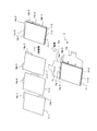
図1に一般的な多層積層液晶パネルの構成を示す。
同図は、R、G及びBの3つの液晶パネル101-1乃至101-3から成る。各液晶パネル101-1乃至101-3にはそれぞれ、接合部104a-1乃至104a-3と接合部104b-1乃至104b-3にドライバIC103-1乃至103-3がマウントされたCOF(Chip On Film)102a-1乃至102a-3と102b-1乃至102b-3が圧着されている。
同図は、R、G及びBの3つの液晶パネル101-1乃至101-3から成る。各液晶パネル101-1乃至101-3にはそれぞれ、接合部104a-1乃至104a-3と接合部104b-1乃至104b-3にドライバIC103-1乃至103-3がマウントされたCOF(Chip On Film)102a-1乃至102a-3と102b-1乃至102b-3が圧着されている。
特許文献1には、3次元表示を行うために、配線部材が接続された複数の液晶パネルを配線部材の接続位置が重ならないように積層配置した表示装置が開示されている。
また特許文献2には、3次元表示を行うために、配線部材が圧着接続された2枚の液晶パネルを特定間隔を空けて重ね合わせた構成の液晶表示装置が開示されている。
また特許文献2には、3次元表示を行うために、配線部材が圧着接続された2枚の液晶パネルを特定間隔を空けて重ね合わせた構成の液晶表示装置が開示されている。
さらに特許文献3には、3次元表示を行うために、配線部材としてフレキシブルプリント基板が長辺に圧着接続された液晶パネルが、所定の間隔を空けて2枚重ね合わせて設けられた構成の液晶表示装置が開示されている。
図1に示した多層積層パネルや、特許文献1乃至3の表示装置はそれぞれ複数の液晶パネルを積層して構成されているが、各パネルそれぞれにCOF等の配線部材を設ける必要がある。図1の場合、1つの液晶パネル101のCOM側の接合部104aとSEG側の接合部104bの2箇所、3枚の液晶パネル101-1乃至101-3で計6ヶ所にそれぞれ1枚ずつ配線部材であるCOFを取り付けなければならない。そしてそのための圧着処理は6回行う必要がある。
特許文献1乃至3の構成の液晶表示装置においても、2つの液晶パネルに1乃至2箇所に、液晶パネルと配線部材を接続する処理を計2乃至4回行う必要がある。また各液晶パネル毎に配線部材を設ける必要がある。
このように液晶パネルと配線部材を接続する処理を多数行うと、製造工程が多くなりその分コスト高となる。また各液晶パネル毎に配線部材を設ける構成の場合、配線部材が多く必要となり、やはりコスト高の要因となる。
そこで本発明は、複数の液晶パネルを積層してなる多層積層パネルにおいて、液晶パネルと配線部材との接続処理にかかるコスト及び配線部材にかかるコストを削減することが出来る多層積層パネルを提供することを目的とする。
本多層積層パネルは、それぞれ形状が異なり、積層したときに接続部がそれぞれ重ならない形状の複数の液晶パネルと、前記複数の液晶パネルの接続部と接続される配線部材と、を備えることを特徴とする。
本配線部材の取付方法は、前記複数の液晶パネルを固定して積層し、
1枚の前記配線部材を1工程で前記複数の液晶パネル全てと接続し、前記複数の液晶パネルを積層するとき、当該液晶パネルに設けた前記配線部材が接続される接続部が重ならないように積層する、ことを特徴とする。
1枚の前記配線部材を1工程で前記複数の液晶パネル全てと接続し、前記複数の液晶パネルを積層するとき、当該液晶パネルに設けた前記配線部材が接続される接続部が重ならないように積層する、ことを特徴とする。
以下、本発明の一実施形態を図面を参照しながら詳細に説明する。
図2は、本実施形態の多層積層パネルの構成原理を説明する図である。
同図は、R、G及びBと色の異なる3つの液晶パネル11-1乃至11-3を対応する各画素が重なるように固定して積層され、多層積層パネル1を構成している。なお以下の説明では3つの液晶パネル11-1乃至11-3を積層して多層積層パネル1を構成する場合を例として説明するが、本実施形態の多層積層パネル1では、積層する液晶パネルの数は3つに限定されるものではない。積層する液晶パネルの数は2つであっても、4つ以上であっても良い。
図2は、本実施形態の多層積層パネルの構成原理を説明する図である。
同図は、R、G及びBと色の異なる3つの液晶パネル11-1乃至11-3を対応する各画素が重なるように固定して積層され、多層積層パネル1を構成している。なお以下の説明では3つの液晶パネル11-1乃至11-3を積層して多層積層パネル1を構成する場合を例として説明するが、本実施形態の多層積層パネル1では、積層する液晶パネルの数は3つに限定されるものではない。積層する液晶パネルの数は2つであっても、4つ以上であっても良い。
この3つの液晶パネル11-1乃至11-3は、COM側とSEG側の端子が設けられ、配線部材12a及び12bと接続される接続部14a-1乃至14a-3と接続部14b-1乃至14b-3を備えている。そして本実施形態の多層積層パネル1で用いられる液晶パネル11-1乃至11-3は、それぞれ形状が異なる。各液晶パネル11-1乃至11-3が備えるCOM側の接続部14a-1乃至14a-3は、3つの液晶パネル11-1乃至11-3を積層したとき、それぞれが互いに重ならないように設けてある。また同様にSEG側の接続部14b-1乃至14b-3も、3つの液晶パネル11-1乃至11-3を積層したときに、それぞれが互いに重ならないように設けてある。
図2では、3つの液晶パネル11-1乃至11-3が積層されて、1つの多層積層パネル1が構成されている。また接続部14a-1乃至14bと接続部14b-1乃至14b-3は、液晶パネル11-1乃至11-3を積層して多層積層パネル1を構成したときに、それぞれ重ならない。よって3つの液晶パネル11-1乃至11-3を固定して積層後にこの接続部14a-1乃至14a-3及び接続部14b-1乃至14b-3に、2枚の配線部材12aと12bを一回の処理で接着することができる。
また配線部材12a及び12bは、COM側及びSEG側でそれぞれ1枚で構成されており、各配線部材12a及び12bは全ての液晶パネル11-1乃至11-3と接続されている。したがって配線部材12aに搭載されたドライバIC13は、液晶パネル11-1乃至11-3全てを1つでドライブすることができる。
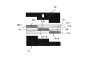
図3に本実施形態の多層積層パネル1の製造工程における積層化した液晶パネル11-1乃至11-3への配線部材12a及び12bの接続工程を示す。
図3は、図2の断面A1-A2から見た図を表している。1-3の接続部12a-1乃至12a-3は、互いに重なりあっていない。
図3は、図2の断面A1-A2から見た図を表している。1-3の接続部12a-1乃至12a-3は、互いに重なりあっていない。
よってこの積層化された液晶パネル11-1乃至11-3をまず受け治具21上に設置し、次にこの液晶パネル11-1乃至11-3の接続部12a-1乃至12a-3に1枚のCOFよりなる配線部材12aの対応位置を合わせて設置する。また同様に不図示の接続部12b-1乃至12b-3に、1枚のCOFよりなる配線部材12bの対応位置を合わせて設置する。そして最後に、上から圧着ヘッド22によって押圧することによって、積層化された液晶パネル11-1乃至11-3の接続部14a-1乃至14a-3及び接続部14b-1乃至14b-3に配線部材12a及び12bが圧着される。
またこの接続処理は1つの工程で実現することができる。
そしてまた積層化された液晶パネル11-1乃至11-3に接続される配線部材12a及び12bをそれぞれ1枚のCOFによって構成することができる。
そしてまた積層化された液晶パネル11-1乃至11-3に接続される配線部材12a及び12bをそれぞれ1枚のCOFによって構成することができる。
本実施形態の多層積層パネル1を構成する液晶パネル11-1乃至11-3は、全て形状が異なり、積層化したとき接続部14a-1乃至14a-3及び14b-1乃至14a-3は、互いに重ならない。このような液晶パネルの形状は、種々考えられるが、以下にその具体的な形状の例を2例挙げる。
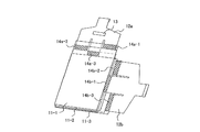
図4は、第1の形状例の液晶パネル11-1乃至11-3によって構成される本実施形態の多層積層パネルの構成例を示す図である。
第1の形状例では、各液晶パネル11-1乃至11-3は、その接続部14a-1乃至14a-3及び14b-1乃至14b-3を図4に示すようにタブ状に設ける。
第1の形状例では、各液晶パネル11-1乃至11-3は、その接続部14a-1乃至14a-3及び14b-1乃至14b-3を図4に示すようにタブ状に設ける。
このタブ状に形成された接続部14a-1乃至14a-3、及び14b-1乃至14b-3は、それぞれ互いに重ならないように形成されている。例えば図4では、COM側では、液晶パネル11-1の接続部14a-1がCOM側の辺1/3より右側に設けられ、液晶パネル11-2の接続部14a-2がCOM側の辺の中央部周辺に設けられ、液晶パネル11-3の接続部14a-3がCOM側の辺1/3より左側に設けられている。同様にSEG側では、液晶パネル11-1の接続部14b-1がSEG側の辺1/3より下側に設けられ、液晶パネル11-2の接続部14b-2がSEG側の辺の中央部周辺に設けられ、液晶パネル11-3の接続部14b-3がSEG側の辺1/3より上側に設けられている。このように設けることによって、液晶パネル11-1乃至11-3が積層された状態において、各接続部14a-1乃至14a-3、及び14b-1乃至14b-3は、重ならない。したがって各接続部14a-1乃至14a-3、及び14b-1乃至14b-3に接続される配線部材は、COM側及びSEG側それぞれ1枚のCOFによって構成することができる。またこの配線部材12a及び12bと積層された液晶パネル11-1乃至11-3との接続処理は、1つの工程によって実現することができる。
この第1の形状例は、各液晶パネル11-1乃至11-3が、フィルム等、形状加工が容易な素材で構成されているときに、特に有効である。
次に第2の形状例について説明する。
次に第2の形状例について説明する。
図5は、第2の形状の液晶パネル11-1乃至11-3によって構成される本実施形態の多層積層パネルの構成例を示す図である。
第2の形状例では、各液晶パネル11-1乃至11-3は、COM側とSEG側の辺をそれぞれ異なる長さで延伸し、この延伸した部分に接続部14a-1乃至14a-3と接続部14b-1乃至14b-3を設ける。
第2の形状例では、各液晶パネル11-1乃至11-3は、COM側とSEG側の辺をそれぞれ異なる長さで延伸し、この延伸した部分に接続部14a-1乃至14a-3と接続部14b-1乃至14b-3を設ける。
図5の例では、COM側の辺を、一番上に積層される液晶パネル11-1ではT11、2番目に積層される液晶パネル11-2ではT12、そして一番下に積層される液晶パネル11-1ではT13だけ延伸しており、その延伸した長さはT11>T12>T13となっている。またSEG側の辺は、一番上に積層される液晶パネル11-1ではT21、2番目に積層される液晶パネル11-2ではT22、そして一番下に積層される液晶パネル11-1ではT23だけ延伸しており、その延伸した長さはT21<T22<T23となっている。よって3つの液晶パネル11-1乃至11-3を上から液晶パネル11-1、液晶パネル11-2、そして液晶パネル11-3の順で積層すると、COM側の延伸部分15a-1乃至15a-3は、段々形状となり、図5の上からみると互いに重ならない部分が生じる。第2の形状ではこの部分に接続部14a-1乃至14a-3を設ける。またSEG側でもその延伸した部分が段々形状となっており、図5の下からみると互いに重ならない部分が生じ、この部分に接続部14b-1乃至14b-3を設ける。
このように重ならないように設けた接続部14a-1乃至14a-3に対して図5の上側から配線部材12aを、また接続部14b-1乃至14b-3に対しては図5の下側から配線部材12bを当て、上下から圧着することにより1つの工程で接続することができる。
このとき配線部材12a及び12bは、それぞれ1枚のCOFによって構成されている。そして各液晶パネル11-1乃至11-3の接続部14a-1乃至14a-3と接続部14b-1乃至14b-3までの距離が異なるので、配線部材12a及び12bは、それぞれの接続部14a-1乃至14a-3と接続部14b-1乃至14b-3に位置が合うように異なる長さで伸ばされ他形状をしている。図5では配線部材12aは、左から順に長くなる形状となっている。また配線部材12bは、下から順に長くなる形状となっている。
この図5に示した第2の形状例の液晶パネル11-1乃至11-3は、形状加工が容易なので、複雑な形状の加工が難しいガラス基板を用いた液晶パネルなどに適用することが特に有効である。
なお図5では、配線部材12aを液晶パネル11-1乃至11-3の図5上で下から接着し、配線部材12bを液晶パネル11-1乃至11-3の図5上で上から接着しているが、逆の構成としても構わない。
なお図4に示した第1の形状例では、SEG側のタブ上の接続部14b-1乃至14b-3において、図面上で一番下に接続部14b-1を持つ液晶パネル11-1を一番上に積層し、接続部14b-2を図面上で真ん中に持つ液晶パネル11-2を真ん中に積層し、接続部14b-3を図面上で一番上に持つ液晶パネル11-3を一番下に積層している。しかし本実施形態の多層積層パネル1の構成はこのようなものに限定されるものではなく、多層積層パネル1の使用状態や機器への実装の仕方等種々の要因によって適宜な形に変更することができる。
図6にその一例を示す。
図6は、図4に示した液晶パネル11-3を図面上で一番上に、液晶パネル11-1をその次に、液晶パネル11-2を一番下に積層して構成した場合の断面A1-A2から見た図を表している。
図6は、図4に示した液晶パネル11-3を図面上で一番上に、液晶パネル11-1をその次に、液晶パネル11-2を一番下に積層して構成した場合の断面A1-A2から見た図を表している。
この場合、図面上で一番上に一番右の接続部14b-3、其の次の段に一番左の接続部14b-1、一番下に真ん中の接続部14b-2が来ている。そして接続部14b-1乃至14b-3に1枚で構成された配線部材12bが接続されている。
このように液晶パネル11-1乃至11-3が第1の形状例の場合、適宜積層する液晶パネルの順番を変更したり、タブ上の接続部を設ける位置を変更することが出来る。
また第2の形状例において、図5においてCOM側では、液晶パネル11-1では図中の一番左に接続部14a-3を、液晶パネル11-2では図中の真ん中に接続部14a-2を、及び液晶パネル11-3では図中の一番右に接続部14a-1を設けていた。また図4においてSEG側では、液晶パネル11-1では図中の一番下に接続部14b-1を、液晶パネル11-2では図中の真ん中に接続部14b-2を、及び液晶パネル11-3では図中の一番上に接続部14b-3を設けていた。しかし本実施形態の多層積層パネル1では、このような配置に限定されるものではなく、多層積層パネル1の使用状態や機器への実装の仕方等種々の要因によって適宜な位置に変更することができる。
また第2の形状例において、図5においてCOM側では、液晶パネル11-1では図中の一番左に接続部14a-3を、液晶パネル11-2では図中の真ん中に接続部14a-2を、及び液晶パネル11-3では図中の一番右に接続部14a-1を設けていた。また図4においてSEG側では、液晶パネル11-1では図中の一番下に接続部14b-1を、液晶パネル11-2では図中の真ん中に接続部14b-2を、及び液晶パネル11-3では図中の一番上に接続部14b-3を設けていた。しかし本実施形態の多層積層パネル1では、このような配置に限定されるものではなく、多層積層パネル1の使用状態や機器への実装の仕方等種々の要因によって適宜な位置に変更することができる。
図7にその一例を示す。
図7では、COM側では、液晶パネル11-1には図中の一番右に接続部14a-1を、液晶パネル11-2には図中の一番左に接続部14a-2を、液晶パネル11-3には図中の真ん中に接続部14a-3を設けている。またSEG側では、液晶パネル11-1には図中の真ん中に接続部14b-1を、液晶パネル11-2には図中の一番上に接続部14b-2を、液晶パネル11-3には図中の一番下に接続部14b-3を設けている。またその位置に合わせて配線部材12a及び12bの形状を変更している。
図7では、COM側では、液晶パネル11-1には図中の一番右に接続部14a-1を、液晶パネル11-2には図中の一番左に接続部14a-2を、液晶パネル11-3には図中の真ん中に接続部14a-3を設けている。またSEG側では、液晶パネル11-1には図中の真ん中に接続部14b-1を、液晶パネル11-2には図中の一番上に接続部14b-2を、液晶パネル11-3には図中の一番下に接続部14b-3を設けている。またその位置に合わせて配線部材12a及び12bの形状を変更している。
このように第2の形状では、各液晶パネル11-1乃至11-3に設ける接続部14a-1乃至14a-3及び14b-1乃至14b-3を設ける位置を適宜に決定することができる。
なお上記説明では、各液晶パネル11-1乃至11-3は、4つの辺のうちの2辺に配線部材12a及び12bを接続する構成を例としてあげているが、本実施形態の多層積層パネル1はこのような構成に限定されるものではない。本実施形態の多層積層パネル1は。液晶パネル11-1乃至11-3の1辺のみに設けられた接続部14-1乃至14-3と1枚の配線部材12を接続する構成であってもよいし、3辺以上と3枚以上の配線部材12都を接続する構成としても良い。
また上記例では、液晶パネル11-1乃至11-3の1つの辺に1つの配線部材を接続する構成としていたが、本実施形態の多層積層パネル1では、複数の辺に設けられた接続部を1つの配線部材で接続する構成としても良い。例えば上記例では、COM側とSEG側を1枚の配線部材で接続する構成としても良い。
また上記例では、積層した液晶パネル11-1乃至11-3と配線部材12a及び12bとの接続は、COM側とSEG側の一回ずつ、計2回の圧着工程によって接続していたが、COM側とSEG側の圧着を同時に行い、1回の工程で接続を行うようにしても良い。
また上記例では、液晶パネル11-1乃至11-3と配線部材12a及び12bの接続を圧着によって行っていたが、液晶パネル11-1乃至11-3内の配線と配線部材12a及び12bとの配線を正確に接続できるものであれば、圧着接続以外の方法であっても良い。
このように本実施形態の多層積層パネルは、その製造工程において、積層した液晶パネルと配線部材との接続作業工程を大幅に削減することができる。また配線部材の量も大幅に削減することができる。さらには、配線部材の枚数を削減することができるので、本実施形態の多層積層パネルを機器に接続する際の工程も削減することができる。
よって、本実施形態の多層積層パネルはその製造コストだけでなく、及び本実施形態の多層積層パネルを用いる機器の製造コストをも削減することができる。
Claims (10)
- それぞれ形状が異なり、積層したときに接続部がそれぞれ重ならない形状の複数の液晶パネルと、
前記複数の液晶パネルの接続部と接続される配線部材と、
を備えることを特徴とする多層積層パネル。 - 前記複数の液晶パネルは、前記接続部をタブ状に備えることを特徴とする請求項1に記載の多層積層パネル。
- 前記複数の液晶パネルは、積層化したとき階段状となる延伸部を備え、前記接続部は前記延伸部上に設けることを特徴とする請求項1に記載の多層積層パネル。
- 前記接続部は、前記複数の液晶パネルの2辺に設けられることを特徴とする請求項1に記載の多層積層パネル。
- 前記配線部分はCOF(Chip On Film)からなることを特徴とする請求項1に記載の多層積層パネル。
- 前記配線部材は、前記複数の液晶パネル全てをドライブするドライバ部を備えることを特徴とする請求項1に記載の多層積層パネル。
- 前記配線部材は、前記複数の液晶パネルに圧着されることを特徴とする請求項1に記載の多層積層パネル。
- 前記配線部材は、前記複数の液晶パネル全てと接続されることを特徴とする請求項1に記載の多層積層パネル。
- 前記複数の液晶パネルは、色がそれぞれ異なる3つの液晶パネルであることを特徴とする請求項1に記載の多層積層パネル。
- 積層した複数の液晶パネルへの配線部材の取付方法であって、
前記複数の液晶パネルを固定して積層し、
1枚の前記配線部材を1工程で前記複数の液晶パネル全てと接続し、
前記複数の液晶パネルを積層するとき、当該液晶パネルに設けた前記配線部材が接続される接続部が重ならないように積層する
ことを特徴とする配線部材の取付方法。
Priority Applications (2)
| Application Number | Priority Date | Filing Date | Title |
|---|---|---|---|
| PCT/JP2011/060490 WO2012147211A1 (ja) | 2011-04-28 | 2011-04-28 | 多層積層パネル及びその配線部材の取付方法 |
| TW101103379A TW201243437A (en) | 2011-04-28 | 2012-02-02 | Multilayer laminate panel and method for attaching wiring member thereof |
Applications Claiming Priority (1)
| Application Number | Priority Date | Filing Date | Title |
|---|---|---|---|
| PCT/JP2011/060490 WO2012147211A1 (ja) | 2011-04-28 | 2011-04-28 | 多層積層パネル及びその配線部材の取付方法 |
Publications (1)
| Publication Number | Publication Date |
|---|---|
| WO2012147211A1 true WO2012147211A1 (ja) | 2012-11-01 |
Family
ID=47071750
Family Applications (1)
| Application Number | Title | Priority Date | Filing Date |
|---|---|---|---|
| PCT/JP2011/060490 Ceased WO2012147211A1 (ja) | 2011-04-28 | 2011-04-28 | 多層積層パネル及びその配線部材の取付方法 |
Country Status (2)
| Country | Link |
|---|---|
| TW (1) | TW201243437A (ja) |
| WO (1) | WO2012147211A1 (ja) |
Citations (1)
| Publication number | Priority date | Publication date | Assignee | Title |
|---|---|---|---|---|
| JP2002169490A (ja) * | 2000-12-01 | 2002-06-14 | Minolta Co Ltd | 積層型表示パネル及び表示装置 |
-
2011
- 2011-04-28 WO PCT/JP2011/060490 patent/WO2012147211A1/ja not_active Ceased
-
2012
- 2012-02-02 TW TW101103379A patent/TW201243437A/zh unknown
Patent Citations (1)
| Publication number | Priority date | Publication date | Assignee | Title |
|---|---|---|---|---|
| JP2002169490A (ja) * | 2000-12-01 | 2002-06-14 | Minolta Co Ltd | 積層型表示パネル及び表示装置 |
Also Published As
| Publication number | Publication date |
|---|---|
| TW201243437A (en) | 2012-11-01 |
Similar Documents
| Publication | Publication Date | Title |
|---|---|---|
| US8780580B2 (en) | Display device | |
| KR101895217B1 (ko) | 타일링 멀티 디스플레이 및 그의 제조 방법 | |
| US10076027B2 (en) | Substrate for connection and display apparatus | |
| US10405437B2 (en) | Display device | |
| WO2023065488A1 (zh) | 一种显示模组及无缝拼接显示装置 | |
| CN110767089B (zh) | 解决曲面显示装置弯曲不良的结构与方法 | |
| CN207009016U (zh) | 显示组件 | |
| TW200540509A (en) | Display device | |
| JP2015207556A (ja) | 発光装置 | |
| KR20160095310A (ko) | 유기 발광 표시 장치 및 그 제조 방법 | |
| US9953600B2 (en) | Display apparatus and method of manufacturing the same | |
| KR20190024270A (ko) | 디스플레이 장치와 이를 포함하는 멀티 스크린 디스플레이 장치 | |
| US20130115818A1 (en) | Pin structure and pin connection structure thereof | |
| CN103676249B (zh) | 用于将多层柔性电路附接至基底的方法和装置 | |
| CN112331090A (zh) | 显示面板、显示模组及拼接屏 | |
| CN103309083A (zh) | 液晶显示装置 | |
| JP2008191502A (ja) | 画像表示素子及びその製造方法 | |
| CN108398818B (zh) | 电光装置以及电子设备 | |
| JP4764293B2 (ja) | 液晶表示装置 | |
| CN102914890A (zh) | 柔性电路板 | |
| TW200528892A (en) | Panel module for an LCD module | |
| US12408528B2 (en) | Method of manufacturing spliced display screen and spliced display screen | |
| WO2012147211A1 (ja) | 多層積層パネル及びその配線部材の取付方法 | |
| JP2008112029A (ja) | 表示装置 | |
| CN113986040A (zh) | 触控显示模组及电子设备 |
Legal Events
| Date | Code | Title | Description |
|---|---|---|---|
| 121 | Ep: the epo has been informed by wipo that ep was designated in this application |
Ref document number: 11864170 Country of ref document: EP Kind code of ref document: A1 |
|
| NENP | Non-entry into the national phase |
Ref country code: DE |
|
| 122 | Ep: pct application non-entry in european phase |
Ref document number: 11864170 Country of ref document: EP Kind code of ref document: A1 |
|
| NENP | Non-entry into the national phase |
Ref country code: JP |