WO2012144043A1 - 半導体集積回路とその動作方法 - Google Patents
半導体集積回路とその動作方法 Download PDFInfo
- Publication number
- WO2012144043A1 WO2012144043A1 PCT/JP2011/059807 JP2011059807W WO2012144043A1 WO 2012144043 A1 WO2012144043 A1 WO 2012144043A1 JP 2011059807 W JP2011059807 W JP 2011059807W WO 2012144043 A1 WO2012144043 A1 WO 2012144043A1
- Authority
- WO
- WIPO (PCT)
- Prior art keywords
- output
- data
- memory
- fifo
- buffer
- Prior art date
- Legal status (The legal status is an assumption and is not a legal conclusion. Google has not performed a legal analysis and makes no representation as to the accuracy of the status listed.)
- Ceased
Links
Images










Classifications
-
- G—PHYSICS
- G06—COMPUTING OR CALCULATING; COUNTING
- G06F—ELECTRIC DIGITAL DATA PROCESSING
- G06F12/00—Accessing, addressing or allocating within memory systems or architectures
- G06F12/02—Addressing or allocation; Relocation
-
- G—PHYSICS
- G06—COMPUTING OR CALCULATING; COUNTING
- G06F—ELECTRIC DIGITAL DATA PROCESSING
- G06F11/00—Error detection; Error correction; Monitoring
- G06F11/07—Responding to the occurrence of a fault, e.g. fault tolerance
- G06F11/16—Error detection or correction of the data by redundancy in hardware
- G06F11/1629—Error detection by comparing the output of redundant processing systems
- G06F11/1641—Error detection by comparing the output of redundant processing systems where the comparison is not performed by the redundant processing components
-
- G—PHYSICS
- G06—COMPUTING OR CALCULATING; COUNTING
- G06F—ELECTRIC DIGITAL DATA PROCESSING
- G06F11/00—Error detection; Error correction; Monitoring
- G06F11/07—Responding to the occurrence of a fault, e.g. fault tolerance
- G06F11/16—Error detection or correction of the data by redundancy in hardware
- G06F11/1666—Error detection or correction of the data by redundancy in hardware where the redundant component is memory or memory area
- G06F11/167—Error detection by comparing the memory output
-
- G—PHYSICS
- G06—COMPUTING OR CALCULATING; COUNTING
- G06F—ELECTRIC DIGITAL DATA PROCESSING
- G06F11/00—Error detection; Error correction; Monitoring
- G06F11/07—Responding to the occurrence of a fault, e.g. fault tolerance
- G06F11/16—Error detection or correction of the data by redundancy in hardware
- G06F11/1675—Temporal synchronisation or re-synchronisation of redundant processing components
- G06F11/1687—Temporal synchronisation or re-synchronisation of redundant processing components at event level, e.g. by interrupt or result of polling
-
- G—PHYSICS
- G06—COMPUTING OR CALCULATING; COUNTING
- G06F—ELECTRIC DIGITAL DATA PROCESSING
- G06F2201/00—Indexing scheme relating to error detection, to error correction, and to monitoring
- G06F2201/845—Systems in which the redundancy can be transformed in increased performance
Definitions
- the present invention relates to a semiconductor integrated circuit and a method for operating the same, and more particularly, to enable continuous write data to be stored in a built-in memory during a multiple redundant operation for testing a semiconductor integrated circuit, while comparing outputs of the multiple redundant operation.
- the present invention relates to an effective technique for reducing the fact that a FIFO for comparison by a device is easily filled with write data.
- Microcontrollers are incorporated into devices such as home appliances, AV devices, mobile phones, automobiles, and industrial machines, and perform various data processing by executing data processing according to programs stored in a memory. This is a semiconductor integrated circuit for controlling the device.
- the in-vehicle microcomputer needs to detect not only these faults by diagnosing various sensors and actuators mounted on the automobile, but also detect the in-vehicle microcomputer itself.
- Non-Patent Document 1 described below describes that a master module and a checker module for comparison simultaneously execute the same processing, and the processing results are compared by a comparison circuit to detect an error.
- Patent Document 1 describes that two CPUs, two memories, and a bus comparator are used, and output signals of the two CPUs are compared by the bus comparator.
- Patent Document 2 three CPUs, three memories, three FIFOs, and three comparison circuits are used, and three output signals from three CPUs are passed through three FIFOs. It is described that the output signals of three CPUs are compared with each other by three comparison circuits.
- Patent Document 3 describes that a plurality of output signals of a plurality of CPUs are compressed by a plurality of compressors, and a plurality of compression results of the plurality of compressors are compared by a comparator.
- the plurality of output signals are supplied to the plurality of inputs of the comparator via the plurality of FIFOs, and the output signals of the plurality of CPUs are compared by the comparator.
- microcontroller microcomputer
- the present inventors first used a comparison method using comparators of output signals of a plurality of CPUs using the FIFO described in Patent Document 3 above. investigated.
- the reason is that the FIFO is a memory that stores and outputs the supplied data without compressing the data in a first-in first-out (First-In / First-Out) method, which enables high-speed storage processing and high-speed output processing. This is because.
- the compressor uses a complicated compression algorithm such as linear feedback shift register (LFSR) and cyclic redundancy check (CRC). There is a disadvantage that the compression processing period becomes long.
- LFSR linear feedback shift register
- CRC cyclic redundancy check
- the CPU which is the core of the microcomputer, has been made high speed and high performance by miniaturization of the semiconductor manufacturing process, and the processing speed of the CPU has been improved year by year.
- the problem that the compression processing period of the compressor is long in the multiple output comparison processing of the CPU for failure diagnosis of the microcomputer is a serious drawback.
- the comparison method using the comparators of the output signals of a plurality of CPUs using the FIFO described in Patent Document 3 has a small circuit scale and power consumption, and can perform high-speed storage processing and high-speed output processing. It is extremely beneficial.
- the amount of data written from the CPU to the FIFO is reduced by operating the CPU at a low speed for a diagnostic test instead of a normal high speed operation during an operation period of a fault diagnosis or a fault test of the microcomputer.
- the CPU processing speed is low speed operation that is significantly lower than the normal high speed operation, another problem that the detection probability of the CPU abnormality or failure is remarkably reduced is clarified by the examination by the present inventors. It was said.
- the present invention has been made as a result of the examination by the present inventors prior to the present invention as described above.
- an object of the present invention is to enable continuous write data to be stored in the built-in memory during the multiple redundant operation for testing the semiconductor integrated circuit, while using the output comparator of the multiple redundant operation. This is to reduce the fact that the FIFO for comparison is easily filled with write data.
- Another object of the present invention is to improve the detection probability of abnormality or failure.
- the semiconductor integrated circuit (1) includes a functional module (2), a built-in memory (3), a first buffer memory (11), and a second buffer memory (12). And a first FIFO memory (13), a second FIFO memory (14), and a comparator (15).
- the first write data output from the functional module during the first operation of the multiple redundant operation for the inspection of the semiconductor integrated circuit is supplied to the built-in memory and the first buffer memory, and the semiconductor integrated circuit includes the first write data.
- Second write data output from the functional module during the second operation of the multiple redundant operation for inspection is supplied to the built-in memory and the second buffer memory.
- the first FIFO memory selects and stores a predetermined number of output times from a plurality of data of the first output data sequentially output from the first buffer memory during the first operation, while the predetermined output Other data of the output count different from the count is not selected.
- the second FIFO memory selects and stores the predetermined number of output data from a plurality of data of the second output data sequentially output from the second buffer memory during the second operation. Other data of the output count different from the output count is not selected.
- the comparator compares the predetermined number of output data selected and output by the first FIFO memory with the predetermined output number of data selected and output by the second FIFO memory. (See FIG. 21).
- continuous write data can be stored in the built-in memory during the multiple redundant operation for the inspection of the semiconductor integrated circuit, while the output of the multiple redundant operation is compared by the comparator. It is possible to reduce the fact that the FIFO for this is easily filled with write data.
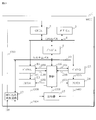
- FIG. 1 is a diagram showing a configuration of a dual core microcomputer MCU1 according to the first embodiment of the present invention.
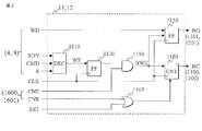
- FIG. 2 is a diagram showing a configuration of buffers A11 and B12 as buffer memories included in the dual core microcomputer MCU1 according to the first embodiment of the present invention shown in FIG.
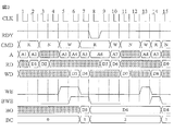
- FIG. 3 is a diagram for explaining the operation of the buffers A11 and B12 as the buffer memory shown in FIG. 2 included in the dual core microcomputer MCU1 according to the first embodiment of the present invention.
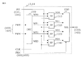
- FIG. 4 is a diagram showing the configuration of FIFO A 13 and B 14 as FIFO memories included in dual-core microcomputer MCU 1 according to the first embodiment of the present invention shown in FIG. FIG.
- FIG. 5 is a diagram for explaining the operations of the FIFOs A and B14 as the FIFO memories shown in FIG. 4 included in the dual core microcomputer MCU1 according to the first embodiment of the present invention.
- FIG. 6 is a diagram showing a configuration of the comparator 15 included in the dual core microcomputer MCU1 according to the first embodiment of the present invention shown in FIG.
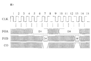
- FIG. 7 is a diagram for explaining the operation of the comparator 15 shown in FIG. 6 included in the dual core microcomputer MCU1 according to the first embodiment of the present invention.
- FIG. 8 is a diagram showing a configuration of the control unit 16 included in the dual core microcomputer MCU1 according to the first embodiment of the present invention shown in FIG.
- FIG. 9 shows a configuration of comparison control register (CCR0) 1610 shown in FIG.
- CCR0 comparison control register
- FIG. 10 shows the configuration of the first comparison control register (CCR1) 1611 and the second comparison control register (CCR2) 1612 shown in FIG. 8 included in the control unit 16 of the dual core microcomputer MCU1 according to the first embodiment of the present invention.
- FIG. 11 is a diagram showing a configuration of the comparison status register (CSR) 1613 shown in FIG. 8 included in the control unit 16 of the dual core microcomputer MCU1 according to the first embodiment of the present invention.
- 12 shows the operations of the FIFOA 13 and B14 shown in FIG. 4 and the operation of the control unit 16 shown in FIG. 8 included in the dual core microcomputer MCU1 according to the first embodiment of the invention shown in FIG.
- FIG. 13 shows the operations of the FIFOA 13 and B14 shown in FIG. 4 and the operation of the control unit 16 shown in FIG. 8 included in the dual-core microcomputer MCU1 according to the first embodiment of the invention shown in FIG.
- FIG. 14 shows the operations of the FIFOA 13 and B14 at the important timings of the operation timing charts of the FIFOA 13 and B14 shown in FIGS. 12 and 13 of the dual core microcomputer MCU1 according to the first embodiment of the invention shown in FIG.
- FIG. 15 shows the operation of the FIFOA 13 and B14 shown in FIG. 4 included in the dual core microcomputer MCU1 according to the first embodiment of the invention shown in FIG. 1 and the operation of the control unit 16 shown in FIG.
- FIG. 16 shows the operations of the FIFOA 13 and B14 shown in FIG. 4 and the operation of the control unit 16 shown in FIG. 8 included in the dual-core microcomputer MCU1 according to the first embodiment of the invention shown in FIG. It is the figure shown to the center.
- FIG. 17 shows the operations of the FIFOA 13 and B14 at the important timings of the operation timing charts of the FIFOA 13 and B14 shown in FIGS. 15 and 16 of the dual core microcomputer MCU1 according to the first embodiment of the invention shown in FIG.
- FIG. 18 shows the operation of the dual-core microcomputer MCU1 according to the first embodiment shown in FIG.
- FIG. 19 is a diagram showing another configuration of buffers A11 and B12 as buffer memories according to the second embodiment of the present invention included in dual core microcomputer MCU1 shown in FIG.
- FIG. 20 is a diagram for explaining the operation of buffer memories A11 and B12 with an arithmetic function according to the second embodiment of the present invention shown in FIG.
- FIG. 21 is a diagram showing a configuration of a single core microcomputer MCU1 according to the third embodiment of the present invention.
- FIG. 22 is a diagram showing a configuration of a triple core microcomputer MCU1 according to the fourth embodiment of the present invention.
- FIG. 23 is a diagram showing a configuration of another triple core microcomputer MCU1 according to the fifth embodiment of the present invention.
- FIG. 24 shows a dual core microcomputer MCU1 according to the first embodiment of the present invention shown in FIGS. 1 to 18 or a buffer memory A11 with an arithmetic function according to the second embodiment of the present invention shown in FIGS.
- It is a figure which shows the structure of the motor vehicle by Embodiment 6 of this invention carrying the triple microcomputer MCU1 by Embodiment 5 of invention.
- a semiconductor integrated circuit (1) includes a functional module (2), a built-in memory (3), a first buffer memory (11), and a second buffer memory (12). ), A first FIFO memory (13), a second FIFO memory (14), and a comparator (15).
- the first write data output from the functional module during the first operation of the multiple redundant operation for the inspection of the semiconductor integrated circuit is supplied to the built-in memory and the first buffer memory, and the semiconductor integrated circuit includes the first write data.
- Second write data output from the functional module during the second operation of the multiple redundant operation for inspection is supplied to the built-in memory and the second buffer memory.
- the first FIFO memory selects and stores a predetermined number of output times from a plurality of data of the first output data sequentially output from the first buffer memory during the first operation, while the predetermined output Other data of the output count different from the count is not selected.
- the second FIFO memory selects and stores the predetermined number of output data from a plurality of data of the second output data sequentially output from the second buffer memory during the second operation. Other data of the output count different from the output count is not selected.
- the comparator compares the predetermined number of output data selected and output by the first FIFO memory with the predetermined output number of data selected and output by the second FIFO memory. (See FIG. 21).
- continuous write data can be stored in the built-in memory during the multiple redundant operation for the inspection of the semiconductor integrated circuit, while the output of the multiple redundant operation is compared with the comparator. It is possible to reduce that the FIFO is easily filled with write data.
- the functional module includes at least a first functional module (2) and a second functional module (6).
- the built-in memory includes at least a first built-in memory (3) and a second built-in memory (7).
- the first write data output from the first functional module during the first operation is supplied to the first built-in memory and the first buffer memory.
- the second write data output from the second functional module during the second operation is supplied to the second built-in memory and the second buffer memory (FIG. 1). reference).
- first functional module and the second functional module are a first central processing unit (2) and a second central processing unit (6), respectively. (See Figure 1).
- the first buffer memory has a first output count of the plurality of data of the first write data sequentially supplied to the first buffer memory during the first operation. (BCA) can be counted.
- the second buffer memory is capable of counting a second output number (BCB) of the plurality of data of the second write data sequentially supplied to the second buffer memory during the second operation. (See FIGS. 2 and 3).
- BCB second output number
- the semiconductor integrated circuit further includes a control unit (16) connected to the first buffer memory, the second buffer memory, the first FIFO memory, and the second FIFO memory (see FIG. 1). ).
- the control unit includes a first register (1625) and a second register (1635) capable of storing the information (4, 8, 12,%) Of the predetermined number of outputs.
- the first FIFO memory In response to the first output count (BCA) counted by the first buffer memory matching the information (FCNA) stored in the first register, the first FIFO memory outputs the predetermined output count.
- the control unit can supply a first FIFO write enable signal (FWEA) for selecting and storing the data to the first FIFO memory.
- FWEA first FIFO write enable signal
- the second FIFO memory In response to the second output count (BCB) counted by the second buffer memory matching the information (FCNB) stored in the second register, the second FIFO memory outputs the predetermined output count.
- the control unit can supply a second FIFO write enable signal (FWEB) for selecting and storing the data to the second FIFO memory (see FIG. 8).
- the contents of the first operation and the second operation of the multiple redundant operation are executed before one of the first central processing unit and the second central processing unit. It is characterized in that it can be the contents of the normal operation that has been performed (see FIG. 18).
- the transition from the normal operation to the multiple redundant operation is performed from any one of the first central processing unit and the second central processing unit executing the normal operation. This is made possible by interruption (204) to the other (see FIG. 18).
- the first buffer memory includes a first flip-flop (1150) for storing the first output data output to the first FIFO memory, one input terminal and the other input.
- a first arithmetic circuit (1170) to which the first write data and the first output data (1101) of the output terminal of the first flip-flop are respectively supplied to the terminals, and an output terminal of the first arithmetic circuit Can be stored in the first flip-flop.
- the second buffer memory has a second flip-flop for storing the second output data output to the second FIFO memory, and the second write data and the second flip-flop at one input terminal and the other input terminal. And a second arithmetic circuit supplied with the second output data of the output terminal of each of the output terminals, and an output signal generated from the output terminal of the second arithmetic circuit can be stored in the second flip-flop. (See FIG. 19).
- a comparison result between the data of the predetermined output number output from the first FIFO memory by the comparator and the data of the predetermined output number output from the second FIFO memory is obtained.
- the semiconductor integrated circuit is determined to be normal if both data match, and the semiconductor integrated circuit is determined to be abnormal if the comparison result indicates a mismatch between both data. (See FIG. 21).
- the first central processing unit executes the instruction for the normal operation stored in the first built-in memory in parallel with the second central processing unit.
- the semiconductor integrated circuit can be operated as a multi-core microcontroller by executing an instruction for normal operation stored in a built-in memory (see FIG. 1).
- a typical embodiment of another aspect of the present invention includes a functional module (2), a built-in memory (3), a first buffer memory (11), a second buffer memory (12), This is an operation method of a semiconductor integrated circuit (1) including a first FIFO memory (13), a second FIFO memory (14), and a comparator (15).
- the first write data output from the functional module during the first operation of the multiple redundant operation for the inspection of the semiconductor integrated circuit is supplied to the built-in memory and the first buffer memory, and the semiconductor integrated circuit includes the first write data.
- Second write data output from the functional module during the second operation of the multiple redundant operation for inspection is supplied to the built-in memory and the second buffer memory.
- the first FIFO memory selects and stores a predetermined number of output times from a plurality of data of the first output data sequentially output from the first buffer memory during the first operation, while the predetermined output Other data of the output count different from the count is not selected.
- the second FIFO memory selects and stores the predetermined number of output data from a plurality of data of the second output data sequentially output from the second buffer memory during the second operation. Other data of the output count different from the output count is not selected.
- the comparator compares the predetermined number of output data selected and output by the first FIFO memory with the predetermined output number of data selected and output by the second FIFO memory. (See FIG. 21).
- continuous write data can be stored in the built-in memory during the multiple redundant operation for the inspection of the semiconductor integrated circuit, while the output of the multiple redundant operation is compared with the comparator. It is possible to reduce that the FIFO is easily filled with write data.
- FIG. 1 is a diagram showing a configuration of a dual core microcomputer MCU1 according to the first embodiment of the present invention.
- the dual-core microcomputer MCU1 according to the first embodiment of the present invention shown in FIG. 1 can compare the outputs of two CPUA2 and CPUB6.
- the internal circuit of the dual core microcomputer MCU1 shown in FIG. 1 is integrated in the semiconductor chip of the semiconductor integrated circuit.
- the CPU A2 as the first central processing unit is a processor that executes processing such as computation and data transfer by executing instructions
- the memory A3 as the first built-in memory stores instructions executed by the CPU A2 and data to be processed.
- the CPUA bus 4 as the first CPU bus is a bus for the CPUA2 to access the device such as the memory A3, and the bridge A5 as the first bus bridge is the case where the CPUA2 accesses the other device via the system bus 10 And a controller for controlling connection between the CPUA bus 4 and the system bus 10.
- the CPU B6 as the second central processing unit is a processor that executes processing such as calculation and data transfer by executing instructions
- the memory B7 as the second built-in memory stores instructions executed by the CPU B6 and data to be processed.
- the CPUB bus 8 as the second CPU bus is a bus for the CPUB6 to access devices such as the memory B7
- the bridge B9 as the second bus bridge is the case where the CPUB6 accesses other devices via the system bus 10
- the buffer A11 as the first buffer memory holds the write data output to the specific address space by the CPU A2, and counts the number of times of output.
- the buffer B12 as the second buffer memory also holds the write data that the CPU B6 outputs to a specific address space, and counts the number of outputs.
- the FIFOA 13 as the first FIFO memory holds the output data 1101 of the buffer A11, while the FIFOB 14 as the second FIFO memory holds the output data 1201 of the buffer B12.
- the technical term “specific address space” here means an address space for double-writing write data output from the CPUs A2 and B6 in the memories A3 and B7 and the buffers A11 and B12.
- the comparator 15 compares the output data 1300 of the FIFO A 13 with the output data 1400 of the FIFO B 14.
- the control unit 16 is connected to the system bus 10 and can be set by the CPU A2 and CPUB6.
- An output signal 1600 of the control unit 16 is a counter clear signal and a data holding / counting permission signal in the buffer A11, while an output signal 1601 of the control unit 16 is a counter clearing signal and a data holding and counting permission signal in the buffer B12. It is.
- the control unit 16 is supplied with a count signal 1100 output from the buffer A11 and a count signal 1200 output from the buffer B12, and the control unit 16 outputs control signals 1602 and 1603 for the FIFOA 13 and the FIFOB14.
- the comparison result signal 1500 from the comparator 15 is supplied to the control unit 16, and the comparison result is held in a register inside the control unit 16. If the comparison results do not match, the control unit 16 can output an interrupt request signal 1604 (C_INTREQ) to the interrupt generation circuit 17.
- the interrupt generation circuit 17 is connected to the system bus 10 and can be set by the CPU A2 and CPUB6. An interrupt request can be supplied from the interrupt request terminal 100 to the interrupt generation circuit 17.
- the dual-core microcomputer MCU 1 includes functional modules such as an A / D converter, a timer, and serial communication, and interrupt requests from these functional modules can be supplied to the interrupt generation circuit 17. ing.
- the interrupt generation circuit 17 priorities are set for a plurality of interrupt requests, the interrupt request with the highest priority is selected, and an interrupt request 1700 from the interrupt generation circuit 17 to the CPU A 2 and an interrupt request 1701 from the CPU B 6 are generated. Is output.
- the dual core microcomputer MCU1 causes the two CPUs A2 and B6 to execute independent data processing in parallel.
- the results of parallel processing by the two CPUs A2 and B6 can be stored in parallel in the two memories A3 and B7.
- the data in the two memories A3 and B7 can be transferred to the system bus 10 via the two bridges A5 and B9.
- the dual core microcomputer MCU1 executes the same data processing in the two CPUs A2 and B6, and detects the mismatch of the processing results. A redundant operation for detecting a failure is executed.
- the two CPUs A2 and B6 execute the same redundant task program for the same operand data.
- the two CPUs A2 and B6 When there is no failure in the dual-core microcomputer MCU1 of FIG. 1 and the two CPUs A2 and B6 are operating normally, the two CPUs A2 and B6 output to a specific address space and the memories A3 and B7 and the buffer The write data that is double-written to A11 and B12 is the same.
- the two CPUs A2 and B6 output the memory A3, Write data that is double-written in B7 and buffers A11 and B12 does not match, and failure detection is possible.
- the two FIFOAs 13 and B14 only output data of a predetermined number of times from a plurality of data sequentially output and supplied as redundant task calculation results from the two CPUs A2 and B6 via the two buffers A11 and B12. While selecting and storing, the data of the number of other outputs is discarded as non-selected. Data of a predetermined number of output times selected and output by the two FIFOAs 13 and B14 are compared by the comparator 15. If the comparison results by the comparator 15 match, it is determined that there is no failure in the dual core microcomputer MCU1 of FIG. 1, and if the comparison results by the comparator 15 do not match, the dual core microcomputer MCU1 of FIG. Is determined to have a fault.
- a plurality of data sequentially output from the two high-performance CPUs A2 and B6 causes the two FIFOAs 13 and B14 to have no free space in a short time, so that the two CPUs A2 and B6 are easily stalled or weighted. This problem can be solved.
- FIG. 2 is a diagram showing a configuration of buffers A11 and B12 as buffer memories included in the dual core microcomputer MCU1 according to the first embodiment of the present invention shown in FIG.
- the buffers A11 and B12 are supplied with the write data WD, the ready signal RDY, the command signal CMD, and the address signal A from the CPUA bus 4 and the CPUB bus 8, and the control unit 16 receives the clock signal CLK, the count enable signal CNE, and the counter reset signal.
- a CNR and a power-on reset signal RST are supplied.
- a decoder (DEC) 1110 is supplied with a ready signal RDY, a command signal CMD, and an address signal A.
- a decoder (DEC) 1110 is provided in response to a high level “1” ready signal RDY indicating that the command signal CMD is valid, a command signal CMD which is a write command, and an address signal A which accesses the buffers A11 and B12.
- a decoder (DEC) 1110 is provided in response to a high level “1” write enable signal WE.
- the write enable signal WE generated from the decoder (DEC) 1110 is supplied to the flip-flop (FF) 1120 in response to the rising edge of the clock CLK.
- the buffer write enable signal BWE generated from the output of the AND circuit 1130 is high level “1”. 1 ".
- the write data WD is stored in the flip-flop (FF) 1150 in response to the rising edge of the clock signal CLK.
- a flip-flop (FF) 1150 generates a buffer output signal BO.
- the counter (CNT) 1160 When the buffer write enable signal BWE is at the high level “1”, the counter (CNT) 1160 counts the clock signal CLK. The counter (CNT) 1160 generates a buffer count signal BC.
- the power-on reset signal RST and the counter reset signal CNR from the control unit 16 are ORed by the OR circuit 1140, and the counter (CNT) 1160 is reset by the output of the OR circuit 1140.
- the addresses of the buffers A11 and B12 as buffer memories are fixed.
- the address range from the start address to the end address can be set by the CPU A2 and CPUB6 in the address setting register. Therefore, the write data to the memories A3 and B7 at arbitrary memory addresses can be buffer-stored in the buffers A11 and B12 by decoding the address signal A in the address range set in the address setting register by the decoder (DEC) 1110. Is possible.
- DEC decoder
- FIG. 3 is a diagram for explaining the operation of the buffers A11 and B12 as the buffer memory shown in FIG. 2 included in the dual core microcomputer MCU1 according to the first embodiment of the present invention.
- the high level “1” ready signal RDY indicates that the command signal CMD is valid
- the low level “0” ready signal RDY indicates that the command signal CMD is invalid.
- the address signal A is output from the CPU A 2 or CPU B 6 to the CPU A bus 4 or CPU bus 8 in a clock cycle based on the clock signal CLK, similarly to the command signal CMD.
- the command signal CMD of the read operation R is output from the CPU A2 or the CPU B6 at the first, second, seventh, ninth and fourteenth of the clock signal CLK.
- the address signal A1, the address signal A2, the address signal A5, the address signal A6, and the address signal A9 are output from the CPU A2 or the CPU B6 at the first, second, seventh, eighth, and fourteenth of the clock signal CLK, respectively.
- the read data RD of the data D1, data D2, data D5, data D6, and data D9 at the second, third, ninth, tenth, and fifteenth of the clock signal CLK is stored in the memory A3 or the memory B7.
- CPUA2 or CPUB6 via CPUA bus 4 or CPU bus 8.
- the command signal CMD of the write operation W is output from the CPU A2 or the CPU B6 at the fifth, sixth, tenth and thirteenth clock signals CLK.
- the address signal A3, the address signal A4, the address signal A7, and the address signal A8 are output from the CPU A2 or the CPU B6 at the fifth, sixth, tenth, and thirteenth clock signal CLK, respectively. Therefore, the write data WD of the data D3, the data D4, and the data D8 is transmitted from the CPU A2 or the CPU B6 to the memory A3 or the memory A3 via the CPUA bus 4 or the CPU bus 8 at the sixth, seventh, and 14th clock signal CLK. The data is written in the memory B7 and the buffer A11 or the buffer B12.
- the tenth address signal A7 of the clock signal CLK is an address other than the memory address for accessing the memory A3 or B7 and the buffer A11 or B12.
- the tenth address signal A7 of the clock signal CLK is for accessing other devices such as a memory mapped I / O.
- the decoder (DEC) 1110 responds to the address signal A3 other than the address signal A7 for accessing other devices, the address signal A4, and the address signal A8, and the fifth and sixth periods of the clock signal CLK. And the write enable signal WE at the high level “1” are generated in the 13th period of the clock signal CLK.
- the flip-flop (FF) 1120 delays the write enable signal WE generated from the output of the decoder (DEC) 1110 by one clock of the clock signal CLK, the buffer write enable of the high level “1” delayed by this one clock.
- Signal BWE is generated from the output of AND circuit 1130.
- the write data WD of the data D3, the data D4, and the data D8 are stored in the flip-flop (FF) 1150, so that the flip-flop (FF) From the output of 1150, a buffer output signal BO of data D3, data D4, and data D8 is generated.
- the counter (CNT) 1160 outputs a buffer count signal BC as the number of times of output of the buffer output signal BO in response to the buffer write enable signal BWE having the high level “1” and the clock signal CLK.
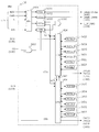
- FIG. 4 is a diagram showing the configuration of FIFO A 13 and B 14 as FIFO memories included in dual-core microcomputer MCU 1 according to the first embodiment of the present invention shown in FIG.
- the FIFO A 13 and B 14 as FIFO memories are composed of four-stage flip-flops (FF) 1310, 1320, 1330, 1340, a decoder (DEC) 1350, and a selector (SEL) 1360. Yes.
- Buffer output signals BO generated from the buffers A11 and B12 as the buffer memory shown in FIG. 2 are supplied to the data input terminals of the four-stage flip-flops (FF) 1310 to 1340.
- a FIFO write enable signal FWE and a FIFO write number signal FWN are supplied from the control unit 16 to the decoder (DEC) 1350, and write enable signals WE0, WE1, WE2, and WE3 are generated from the decoder (DEC) 1350.
- the FIFO lead number signal FRN is supplied from the control unit 16 to the selector (SEL) 1360, and the output signals FO0, FO1, FO2, and FO3 of the flip-flops (FF) 1310, 1320, 1330, and 1340 indicated by the FIFO lead number signal FRN are displayed. Is selected and becomes the FIFO output signal FO.
- FIG. 5 is a diagram for explaining the operations of the FIFOs A and B14 as the FIFO memories shown in FIG. 4 included in the dual core microcomputer MCU1 according to the first embodiment of the present invention.
- FIG. 5 shows that only the last one of the four buffer output signals BO sequentially supplied from the buffers A11 and B12 to the FIFOA 13 and B14 is stored in the FIFOA 13 and B14. That is, only the last one data input signal D4 among the four data output signals D1, D2, D3, and D4 as the four buffer output signals BO that are sequentially supplied is stored in the FIFO A13 and B14, and then supplied sequentially. Of the four data output signals D5, D6, D7, and D8 as the four buffer output signals BO, only the last one data input signal D8 is stored in the FIFOA 13 and B14.
- the FIFO write number signal FWN and the FIFO read number signal FRN are initially set to an initial value “0” by the control unit 16.
- the FIFO write enable signal FWE is controlled to the high level “1” by the control unit 16 at the rising timing of the eighth clock signal CLK, so that the fourth data input signal D4 becomes the rising edge of the ninth clock signal CLK. It is stored in the first stage flip-flop (FF) 1310 at the timing.
- the output signal FO0 of the first-stage flip-flop (FF) 1310 is selected by the selector (SEL) 1360 to be the FIFO output signal FO. Outputs the fourth data input signal D4.
- the control unit 16 performs the FIFO write number signal FWN. Is changed from the initial value “0” to the next updated value “1”.
- the comparator 15 in the dual core microcomputer MCU1 according to the first embodiment of the present invention shown in FIG. Comparison of the FIFO output signals FO of both the two FIFOA 13 and FIFOOB 14 is executed. After this comparison is executed, the fourth data input signal D4 stored in the two FIFOA 13 and FIFOB 14 becomes unnecessary. In the example shown in FIG. 5, the fourth data input signal D4 is already stored in one of the two FIFOA 13 and FIFOB 14 at the rise timing of the eighth clock signal CLK, and the rise of the eleventh clock signal CLK.
- the fourth data input signal D4 is stored in the other of the two FIFOA13 and FIFOOB14, and the comparator 15 compares the two FIFO output signals FO of the two FIFOA13 and FIFOOB14.
- the FIFO output signal FO is indefinite.
- the control unit 16 changes the FIFO read number signal FRN from the initial value “0” to the next update value “1”. To do.
- the eighth data input signal D8 Is stored in the second-stage flip-flop (FF) 1320 at the rise timing of the 14th clock signal CLK.
- the eighth data input signal D8 is stored in the second-stage flip-flop (FF) 1320 in this way because the control unit 16 changes the FIFO write number signal FWN from the initial value “0” to the update value “1”. This is because it has been changed.
- the output signal FO1 of the second-stage flip-flop (FF) 1320 is selected by the selector (SEL) 1360 and becomes the FIFO output signal FO. Outputs the eighth data input signal D8.
- FIG. 6 is a diagram showing a configuration of the comparator 15 included in the dual core microcomputer MCU1 according to the first embodiment of the present invention shown in FIG.
- the comparator 15 includes a digital comparator 1510.
- the FIFO output signal FOA (1300) of the FIFOA 13 and the FIFO output signal of the FIFO B 14 are connected to one input terminal and the other input terminal of the digital comparator 1510, respectively.
- FOB (1400) is supplied, and the comparison output signal CO is generated from the output terminal of the digital comparator 1510.
- the comparison output signal CO becomes the low level “1”, while the FIFO output signal FOA (1300) of the FIFOA 13 ) And the FIFO output signal FOB (1400) of the FIFOB 14 do not coincide with each other, the comparison output signal CO becomes the high level “1”.
- FIG. 7 is a diagram for explaining the operation of the comparator 15 shown in FIG. 6 included in the dual core microcomputer MCU1 according to the first embodiment of the present invention.
- the fourth data input signal D4 is output in the period of the fifth to seventh clock signals CLK, and the tenth to thirteenth.
- the eighth data input signal D8 is output during the period of the clock signal CLK and becomes indefinite during other periods.
- the FIFO output signal FOB (1400) of the FIFOB 14 the fourth data input signal D4 is output in the period of the seventh clock signal CLK, and the other eighth data in the period of the thirteenth clock signal CLK.
- An input signal D8 ′ (a value different from the eighth data input signal D8) is output, and becomes indefinite in other periods.
- a comparison output signal CO having a low level “0” (both inputs coincide) is generated in the period of the seventh clock signal CLK, and a high level “1” (both both) is generated in the period of the thirteenth clock signal CLK.
- the comparison output signal CO with the input mismatched is generated, and the comparison output signal CO is invalid during other periods.
- FIG. 8 is a diagram showing a configuration of the control unit 16 included in the dual core microcomputer MCU1 according to the first embodiment of the present invention shown in FIG.
- control unit 16 includes a decoder (DEC) 1614, a comparison control register (CCR0) 1610, a first comparison control register (CCR1) 1611, a second comparison control register (CCR2) 1612, The comparison state register (CSR) 1613, a 3-input AND circuit 1615, a 2-input AND circuit 1616, a first control unit (CTA) 1626, a second control unit (CTB) 1636, and the like are included.
- DEC decoder
- CCR0 comparison control register
- CCR1 first comparison control register
- CCR2 second comparison control register
- CSR The comparison state register
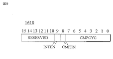
- FIG. 9 is a diagram showing a configuration of the comparison control register (CCR0) 1610 shown in FIG. 8 included in the control unit 16 of the dual core microcomputer MCU1 according to the first embodiment of the present invention.
- CCR0 comparison control register
- bits 7 to 0 of the comparison control register (CCR0) 1610 are the comparison cycle CMPCYC, and each of the plurality of buffer output signals BO sequentially generated from the buffers A11 and B12 is FIFOA13, 14 is set and how many are compared by the comparator 15 is set.
- H00 of all “0” indicates the comparison cycle 256
- set values H01 to HFF that are values excluding all “0” are the comparison cycles 1 to 255.
- the set value of the comparison cycle CMPCYC in bits 7 to 0 of the comparison control register (CCR0) 1610 shown in FIG. 9 can be determined by the value of the write data WD from the system bus 10.
- Bit 8 of the comparison control register (CCR0) 1610 in FIG. 9 is a comparison enable signal CMPEN. For example, a low level “0” indicates that comparison is prohibited and a high level “1” indicates that comparison is permitted.
- Bit 9 of the comparison control register (CCR0) 1610 in FIG. 9 is an interrupt enable signal INTEN. For example, a low level “0” indicates interrupt prohibition, and a high level “1” indicates interrupt permission.
- bits 15 to 10 of the comparison control register (CCR0) 1610 are reserved bits RESERVED.
- FIG. 10 shows the configuration of the first comparison control register (CCR1) 1611 and the second comparison control register (CCR2) 1612 shown in FIG. 8 included in the control unit 16 of the dual core microcomputer MCU1 according to the first embodiment of the present invention.
- CCR1 first comparison control register
- CCR2 second comparison control register
- bit 0 is the count enable signal CNTEN, and in the case of the first comparison control register (CCR1) 1611, it is set whether or not the output data of the CPU A2 is held in the buffer A11 and counted. In the case of the second comparison control register (CCR2) 1612, whether to count the output data of the CPU B6 in the buffer B12 is set. For example, holding and counting are not executed at the low level “0”, and holding and counting are executed at the high level “1”.
- Bit 1 in FIG. 10 is a count reset signal CNTRST. In the case of the first comparison control register (CCR1) 1611, the counter reset of the buffer A11 is executed, while in the case of the second comparison control register (CCR2) 1612, the buffer is reset.
- B12 counter reset is executed.
- the buffer counter reset is not executed at the low level “0”, and the buffer counter reset is executed at the high level “1”.
- CNTRST does not hold the written value, but detects that the high level “1” is written, and resets the counters of the buffers A11 and B12.
- bits 15 to 2 are reserved bits RESERVED.
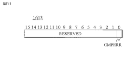
- FIG. 11 is a diagram showing a configuration of the comparison status register (CSR) 1613 shown in FIG. 8 included in the control unit 16 of the dual core microcomputer MCU1 according to the first embodiment of the present invention.
- CSR comparison status register
- bit 0 of the comparison status register (CSR) 1613 is the comparison error signal CMPERR.
- CMPERR comparison error signal
- a low level “0” indicates no comparison error (comparison result coincidence), while a high level “1”. Indicates a comparison error (comparison result mismatch).
- CMPERR comparison error signal
- bits 15 to 1 are reserved bits RESERVED.
- the ready signal RDY, the command signal CMD, and the address signal A of the system bus 10 are decoded by the decoder (DEC) 1614, the comparison control register (CCR0) 1610, the first comparison control register (CCR1) 1611, Write control of write data WD to the second comparison control register (CCR2) 1612 and the comparison status register (CSR) 1613 is executed.
- various write data WD written to the comparison control register (CCR0) 1610, the first comparison control register (CCR1) 1611, the second comparison control register (CCR2) 1612, and the comparison status register (CSR) 1613 of the control unit 16 are Can be supplied from the on-chip built-in nonvolatile memory (not shown) of the dual-core microcomputer MCU1 via the system bus 10, and via the system bus 10 and the direct memory access controller (DMAC). It can also be supplied from an off-chip external non-volatile memory (not shown) mounted on the motherboard.
- DMAC direct memory access controller
- the system bus includes a comparison control register (CCR0) 1610, a first comparison control register (CCR1) 1611, a second comparison control register (CCR2) 1612, and a comparison status register (CSR) 1613. It is also possible to add a function of executing read control to 10 and outputting read data RD to the system bus 10.
- CCR0 comparison control register
- CCR1 first comparison control register
- CCR2 second comparison control register
- CSR comparison status register
- the interrupt enable signal INTEN from the comparison control register (CCR0) 1610 and the comparison error signal CMPERR from the comparison status register (CSR) 1613 are logically ANDed by the 2-input AND circuit 1616, and an interrupt is generated from the output of the 2-input AND circuit 1616.
- a comparison error interrupt signal C_INTREQ to the circuit 17 is generated.
- the first comparison control register (CCR1) 1611 generates a count enable signal CNEA and a counter reset signal CNRA supplied to the buffer A11.
- the second comparison control register (CCR2) 1612 generates a count enable signal CNEB and a counter reset signal CNRB supplied to the buffer B12.
- the register (FC0A) 1620, the register (FC1A) 1621, the register (FC2A) 1622, and the register (FC3A) 1623 as FIFO counters store data sequentially generated from the buffer A11. This holds data indicating how many pieces of data are stored in the flip-flop (FF) 1310, flip-flop (FF) 1320, flip-flop (FF) 1330, and flip-flop (FF) 1340 of the FIFOA 13, respectively. is there.
- the register (FSTA) 1624 holds the state (data presence / absence) of the output signals FO0, FO1, FO2, and FO3 of the flip-flops (FF) 1310, 1320, 1330, and 1340 of the FIFOA 13.
- the register (FCNA) 1625 holds information on what number of buffer output signals BO to be held next in the FIFO A 13 are generated from the buffer A 11.
- a control unit (CTA) 1626 executes control of the registers 1620, 1621, 1622, 1623, 1624, and 1625 described above.
- the control unit (CTA) 1626 receives the comparison enable signal CMPEN and the comparison cycle CMPCYC from the comparison control register (CCR0) 1610, and receives the buffer count signal BCA from the buffer A11. First, when writing is performed to the comparison control register (CCR0) 1610, the comparison cycle CMPCYC is copied to the register (FCNA) 1625.
- the control unit (CTA) 1626 compares the buffer count signal BCA with the contents of the register (FCNA) 1625, and if they match, the register (FSTA) 1624 stores data in the registers 1620, 1621, 1622, and 1623 as FIFO counters.
- the buffer count signal BCA is stored in the register which is initially indicated as not including.
- the control unit (CTA) 1626 outputs the FIFO write enable signal FWEA and the FIFO write number signal FWNA to the FIFOA 13, and writes the buffer output signal BOA supplied from the buffer A11 to the FIFOA 13.
- the control unit (CTA) 1626 writes an added value of the value of the buffer count signal BCA and the value of the comparison cycle CMPCYC at that time into the register (FCNA) 1625.
- the register (FC0B) 1630, the register (FC1B) 1631, the register (FC2B) 1632, and the register (FC3B) 1633 as FIFO counters store data sequentially generated from the buffer B12. It holds data indicating how many pieces of data are stored in the flip-flop (FF) 1310, flip-flop (FF) 1320, flip-flop (FF) 1330, and flip-flop (FF) 1340 of the FIFOOB 14, respectively. is there.
- the register (FSTB) 1634 holds the states (data presence / absence) of the output signals FO0, FO1, FO2, and FO3 of the flip-flops (FF) 1310, 1320, 1330, and 1340 of the FIFOOB14.
- the register (FCNB) 1635 holds information on what number the buffer output signal BO to be held next in the FIFO B 14 is generated from the buffer B 12.
- the control unit (CTB) 1636 executes control of the registers 1630, 1631, 1632, 1633, 1634, and 1635 described above.
- the control unit (CTB) 1636 receives the comparison enable signal CMPEN and the comparison cycle CMPCYC from the comparison control register (CCR0) 1610, and receives the buffer count signal BCB from the buffer B12. First, when writing is performed to the comparison control register (CCR0) 1610, the comparison cycle CMPCYC is copied to the register (FCNB) 1635.
- the control unit (CTB) 1636 compares the buffer count signal BCB with the contents of the register (FCNB) 1635. If the two match, the register (FSTB) 1634 stores data from the registers 1630, 1631, 1632 and 1633 as FIFO counters. The buffer count signal BCB is stored in the register which is first shown as not including. At the same time, the control unit (CTB) 1636 outputs the FIFO write enable signal FWEB and the FIFO write number signal FWNB to the FIFO B 14 and writes the buffer output signal BOB supplied from the buffer B 12 to the FIFO B 14. The control unit (CTB) 1636 writes an addition value of the value of the buffer count signal BCB and the value of the comparison cycle CMPCYC at that time into the register (FCNB) 1635.
- the buffer output signal BOA supplied from the buffer A11 cannot be written to the FIFOA 13.
- the comparison by the comparator 15 is executed and a space is created in the FIFO A 13.
- the buffer count signal BCA at that time is written into the empty FIFO counter, and the added value of the value of the buffer count signal BCA and the value of the comparison cycle CMPCYC is written into the register (FCNA) 1625. Further, the buffer output signal BOA at that time is written into the FIFOA 13.
- the writing of the buffer output signal BOB from the buffer B12 is interrupted every integral multiple of the comparison cycle CMPCYC, so that the number of writes of the buffer output signal BOB is skipped. Therefore, when this skip occurs, it is necessary to notify the FIFO A 14 of the skip occurrence from the FIFO B 14.
- the FIFOA 13 notified of the occurrence of the skip updates the contents of the FIFO counter of the FIFOA 13 according to the skip. When the FIFOA 13 skips the number of writes of the buffer output signal BOA, it is necessary to notify the FIFO B 14 of the skip occurrence from the FIFO A 13.
- the FIFOB 14 notified of the occurrence of the skip updates the contents of the FIFO counter of the FIFOA 13 according to the skip. That is, the internal signal 1627 is used to notify the occurrence of a skip from the FIFOA 13 to the FIFOB 14, and the internal signal 1637 is used to notify the occurrence of a skip from the FIFOB 14 to the FIFOA 13.
- the control unit (CTA) 1626 sets the comparison enable signal CEA to the low level “0” when there is no valid data in the FIFOA 13, and sets it to the high level “1” when there is valid data in the FIFOA 13. To do. Similarly, the control unit (CTB) 1636 sets the comparison enable signal CEB to the low level “0” when there is no valid data in the FIFOB 14, while the high level “1” when there is valid data in the FIFOB 14. Set to.
- the comparison enable signal CEA and the comparison enable signal CEB become high level “1”
- the comparison output signal CO of the comparator 15 is written to the comparison error signal CMPERR of the comparison status register (CSR) 1613 via the 3-input AND circuit 1615. It is.
- the comparison error signal CMPERR in the comparison status register (CSR) 1613 can be cleared by writing the clear signal H0000 in the comparison status register (CSR) 1613.
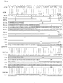
- FIG. 12 shows the operations of the FIFOA 13 and B14 shown in FIG. 4 and the operation of the control unit 16 shown in FIG. 8 included in the dual core microcomputer MCU1 according to the first embodiment of the invention shown in FIG. It is the figure shown to the center.
- FIG. 13 shows the operations of the FIFOA 13 and B14 shown in FIG. 4 and the operation of the control unit 16 shown in FIG. 8 included in the dual-core microcomputer MCU1 according to the first embodiment of the invention shown in FIG. It is the figure shown to the center.
- bits 7 to 0 of the comparison control register (CCR0) 1610 of the control unit 16 are set to the value “H04” as a predetermined initial value in the comparison cycle CMPCYC. .
- the value of the buffer count signal BCA supplied from the buffer A11 to the control unit (CTA) 1626 of the control unit 16 is “3” and is connected to the control unit (CTA) 1626.
- the contents of the register (FCNA) 1625 are “4”, and the contents of the register (FSTA) 1624 are “H0 (no data)”.
- the value of the buffer count signal BCA supplied from the buffer A11 becomes “4” and matches the content “4” of the register (FCNA) 1625 at the ninth clock signal CLK in FIG. 12, the next tenth clock signal CLK.
- the value “4” of the buffer count signal BCA is written as the content FC0A of the register (FC0A) 1620 connected to the control unit (CTA) 1626.
- the added value “8” of the value “4” of the buffer count signal BCA at this time and the value “4” of the comparison cycle CMPCYC is stored in the register (FCNA) 1625.
- the read data FOA of the FIFOA 13 is included in the first stage flip-flop ( FF) 1310 data FO0 is selected, and data D4 is output from the timing of the tenth clock signal CLK. Further, the value of the comparison enable signal CEA supplied from the control unit (CTA) 1626 to the three-input AND circuit 1615 becomes high level “1”.
- the contents of the register (FSTB) 1634 are changed from “H0 (no data)” to “H1 (FO0 has data)”.
- the read data FOB of the FIFOB 14 is included in the first flip-flop.
- the data FO0 of (FF) 1310 is selected, and the data D4 is output from the timing of the 20th clock signal CLK. Further, the value of the comparison enable signal CEB supplied from the control unit (CTB) 1636 to the 3-input AND circuit 1615 becomes the high level “1”.
- the comparator 15 compares the FIFO output signal FOA (1300) and the FIFO output signal FOB (1400), which are the same data, the first-stage flip-flop (FF) 1310 of the FIFOA 13 becomes empty.
- the read data FOB of the FIFOB 14 has a second stage flip-flop (FF).
- the data FO1 (undefined) 1320 is selected, and the FIFO output signal FOB (1400) of the FIFOOB 14 is undefined at the timing of the 21st clock signal CLK.
- the value “12” of the buffer count signal BCA at this time and the added value “16” of the value “4” of the comparison cycle CMPCYC are written to the register (FCNA) 1625, and the register The content of (FSTA) 1624 is changed from “H2 (with data in FO1)” to “H6 (with data in FO1 and FO2)”. Further, at the timing of the 30th clock signal CLK, the write enable signal FWEA supplied from the control unit (CTA) 1626 to the FIFOA 13 is already at the high level “1”, so that the FIFOA 13 outputs the buffer output supplied from the buffer A11.
- the comparison enable signal CEA and the comparison enable signal CEB are both at the high level “1” at the timing of the 31st clock signal CLK, the FIFO output signal FOA (1300) of the FIFOA 13 and the FIFO output of the FIFOB 14
- the comparison of the FIFO output signal FOA (1300) and the FIFO output signal FOB (1400), which are the same data, is performed by the comparator 15 at the timing of the 31st clock signal CLK.
- the second-stage flip-flop (FF) 1320 becomes empty, and the content of the register (FSTB) 1634 is changed from “H2 (with data in FO1)” to “H0 (no data)”. Since the value of the FIFO read number signal FRNB supplied from the control unit (CTB) 1636 to the FIFOB 14 has been changed from “1” to “2”, the read data FOB of the FIFOOB 14 has a third stage flip-flop (FF).
- the data FO2 (undefined) 1330 is selected, and the FIFO output signal FOB (1400) of the FIFOOB 14 is undefined at the timing of the 32nd clock signal CLK.
- FIG. 14 shows the operations of the FIFOA 13 and B14 at the important timings of the operation timing charts of the FIFOA 13 and B14 shown in FIGS. 12 and 13 of the dual core microcomputer MCU1 according to the first embodiment of the invention shown in FIG. FIG.
- the partial diagrams (1-A) to (6-A) of FIG. 14 are the timing (1), timing (2), and timing (3) of the operation timing charts of the FIFOA 13 and B14 shown in FIGS. ), Timing (4), timing (5), and timing (6), the operation of the FIFOA 13 is shown.
- the partial diagrams (1-B) to (6-B) in FIG. 14 show timing (1) and timing (2) in the operation timing charts of the FIFOA 13 and B14 shown in FIGS.
- the operation of the FIFOB 14 at timing (3), timing (4), timing (5), and timing (6) is shown.
- the contents of the FIFO counter register (FC0A) 1620, register (FC1A) 1621, register (FC2A) 1622, register (FC3A) 1623, and four-stage flip-flop (FIFOA13) FF) The contents of the output signals FO0, FO1, FO2, and FO3 of 1310, 1320, 1330, and 1340 are all invalid, the contents of the register (FSTA) 1624 are “H0 (no data)”, and the register (FCNA) The content of 1625 is “4”. Therefore, in the FIFOA 13 in the state shown in the partial diagram (1-A) of FIG.
- the contents of the output signals FO0, FO1, FO2, and FO3 of 1310, 1320, 1330, and 1340 are all invalid
- the contents of the register (FSTA) 1624 are “H0 (no data)”
- the content of 1635 is “4”. Therefore, in the FIFOOB 14 in the state shown in the partial diagram (1-B) of FIG.
- the buffer count signal is set as the content FC0A of the register (FC0A) 1620 of the FIFO counter.
- the added value “8” of the value “4” of the buffer count signal BCA and the value “4” of the comparison cycle CMPCYC is written to the register (FCNA) 1625, and the content of the register (FSTA) 1624 is “H0”.
- No data) is changed to“ H1 (data is in FO0)
- the FIFO write number signal FWNA value is changed from“ 0 ”to“ 1 ”.
- the buffer count signal is used as the content FC1A of the register (FC1A) 1621 of the FIFO counter.
- the added value “12” of the value “8” of the buffer count signal BCA and the value “4” of the comparison cycle CMPCYC is written into the register (FCNA) 1625, and the content of the register (FSTA) 1624 is “H1 ( “FO0 has data” is changed to “H3 (FO0 and FO1 have data)”, and the FIFO write number signal FWNA value is changed from “1” to “2”.
- the value of the FIFO write number signal FWNB is changed from “1” to “2”.
- FIG. 15 shows the operation of the FIFOA 13 and B14 shown in FIG. 4 included in the dual core microcomputer MCU1 according to the first embodiment of the invention shown in FIG. 1 and the operation of the control unit 16 shown in FIG. It is the figure shown to the center.
- FIG. 15 is an operation timing chart following the operation timing chart shown in FIG.
- FIG. 16 shows the operations of the FIFOA 13 and B14 shown in FIG. 4 and the operation of the control unit 16 shown in FIG. 8 included in the dual-core microcomputer MCU1 according to the first embodiment of the invention shown in FIG. It is the figure shown to the center.
- FIG. 16 is an operation timing chart continued from the operation timing chart shown in FIG.
- the value of the buffer count signal BCA supplied from the buffer A 11 to the control unit (CTA) 1626 of the control unit 16 is “15” and is connected to the control unit (CTA) 1626.
- the content of the register (FCNA) 1625 is “16”
- the content of the register (FSTA) 1624 is “H4 (there is data in FC2)”.
- the sixth clock signal CLK when the value of the buffer count signal BCA supplied from the buffer A11 is “16” and matches the content “16” of the register (FCNA) 1625, the next seventh clock signal CLK
- the value “16” of the buffer count signal BCA is written as the content 3A of the register (FC3A) 1623 connected to the control unit (CTA) 1626.
- an addition value “20” of the value “16” of the buffer count signal BCA at this time and the value “4” of the comparison cycle CMPCYC is written to the register (FCNA) 1625.
- the content of the register (FSTA) 1624 becomes “HC (data exists in FO2 and FO3)”.
- the value of the buffer count signal BCA supplied from the buffer A11 is “20” and matches the content “20” of the register (FCNA) 1625 in the 16th clock signal CLK, the next 17th clock signal CLK.
- the value “20” of the buffer count signal BCA is written as the content FC0A of the register (FC0A) 1620 connected to the control unit (CTA) 1626 at the timing of the clock signal CLK.
- CTA control unit
- an addition value “24” of the value “20” of the buffer count signal BCA at this time and the value “4” of the comparison cycle CMPCYC is written to the register (FCNA) 1625.
- the content of the register (FSTA) 1624 is changed from “HC (data exists in FO2 and FO3)” to “HD (data exists in FO2, FO3, FO0)”.
- the write enable signal FWEA supplied from the control unit (CTA) 1626 to the FIFOA 13 is already at the high level “1”, so that the FIFOA 13 receives the buffer supplied from the buffer A11.
- the value of the buffer count signal BCA supplied from the buffer A11 is “24”, and when it matches the content “24” of the register (FCNA) 1625, the next 23rd clock signal CLK.
- the value “24” of the buffer count signal BCA is written as the content FC1A of the register (FC0A) 1621 connected to the control unit (CTA) 1626 at the timing of the clock signal CLK.
- the added value “28” of the value “24” of the buffer count signal BCA at this time and the value “4” of the comparison cycle CMPCYC is written to the register (FCNA) 1625.
- the content of the register (FSTA) 1624 is changed from “HD (with data in FO2, FO3, FO0)” to “HF (with data in FO2, FO3, FO0, FO1)”. Furthermore, at the timing of the 21st clock signal CLK, the write enable signal FWEA supplied from the control unit (CTA) 1626 to the FIFOA 13 is already at the high level “1”, so the FIFOA 13 receives the buffer supplied from the buffer A11.
- the value of the buffer count signal BCA supplied from the buffer A11 is “28”, which matches the content “28” of the register (FCNA) 1625.
- the value of the buffer count signal BCB supplied from the buffer B12 to the control unit (CTB) 1636 of the control unit 16 is “12”, and the register (FCNB) 1635 If it matches the content “12”, the value “12” of the buffer count signal BCB is written as the content FC2B of the register (FC2B) 1632 connected to the control unit (CTB) 1636 at the timing of the next 31st clock signal CLK. It is.
- the comparison enable signal CEA and the comparison enable signal CEB are at the high level “1”
- the FIFO output signal FOA (1300) of the FIFOA 13 and the FIFO output signal FOB (1400) of the FIFOOB 14 are compared.
- the FIFOA 13 causes a vacancy in the third stage flip-flop (FF) 1330 with the 31st clock signal CLK.
- the register (FC2A) connected to the control unit (CTA) 1626 at the timing of the next 31st clock signal CLK when the value “31” of the buffer count signal BCA supplied from the buffer A11 is the 32nd clock signal CLK.
- the value “31” of the buffer count signal BCA is written as the content FC2A of 1622.
- FIG. 17 shows the operations of the FIFOA 13 and B14 at the important timings of the operation timing charts of the FIFOA 13 and B14 shown in FIGS. 15 and 16 of the dual core microcomputer MCU1 according to the first embodiment of the invention shown in FIG. FIG.
- the partial diagrams (1-A) to (6-A) in FIG. 17 are the timing (1), timing (2), and timing (3) of the operation timing charts of the FIFOA 13 and B14 shown in FIGS. ), Timing (4), timing (5), and timing (6), the operation of the FIFOA 13 is shown.
- the partial diagrams (1-B) to (6-B) in FIG. 17 show timing (1) and timing (2) in the operation timing charts of the FIFOA 13 and B14 shown in FIG. 15 and FIG.
- the operation of the FIFOB 14 at timing (3), timing (4), timing (5), and timing (6) is shown.
- the value of the buffer count signal BCA supplied from the buffer A11 to the control unit (CTA) 1626 of the control unit 16 is “15” and is connected to the control unit (CTA) 1626.
- the content of the registered register (FCNA) 1625 is “16”
- the other registers (FC0A) 1620, (FC1A) 1621, (FC3A) 1623 and the other flip-flops (FF) 1310, 1320, 1340 are invalid.
- the content of the register (FSTA) 1624 is “H4 (with data in FO2)”, the value of the FIFO read number signal FRNA is “2 (FO2)”, and the value of the FIFO write number signal Is “3 (FO3)”.
- the contents of the FIFO counter register (FC0B) 1630, the register (FC1B) 1631, the register (FC2B) 1632, the register (FC3B) 1633, and the four-stage flip-flop (FIFOB14) FF) The contents of the output signals FO0, FO1, FO2, and FO3 of 1310, 1320, 1330, and 1340 are all invalid, the contents of the register (FSTA) 1624 are “H0 (no data)”, and the register (FCNB) The content of 1635 is “12”. Accordingly, in the FIFOB 14 in the state shown in the partial diagram (1-B) of FIG.
- the value “16” of the buffer count signal BCA is the register (FC3A) 1623.
- the added value “20” of the value “16” of the buffer count signal BCA and the value “4” of the comparison cycle CMPCYC is written to the register (FCNA) 1625, and the content of the register (FSTA) 1624 is “H4”.
- the data is updated from “there is data in FO2” to “HC (there is data in FO2 and FO3)”.
- the value of the FIFO write number signal FWNA is updated from “3” to “0”, and the value of the FIFO read number signal FRNA is maintained at “2 (FO2)”.
- the value of the buffer count signal BCA supplied from the buffer A11 is “20”, which matches the content “20” of the register (FCNA) 1625. Therefore, the content of the register (FC0A) 1620
- the buffer count signal BCA value “20” is written as FC0A
- the value of the buffer count signal BCB supplied from the buffer B12 to the control unit (CTB) 1636 of the control unit 16 is “11”
- the content of the register (FCNB) 1635 is At “12”
- the content of the register (FSTB) 1634 is “0 (no data)”
- the value of the buffer count signal BCA supplied from the buffer A11 is “24”, which matches the content “24” of the register (FCNA) 1625. Therefore, the content of the register (FC0A) 1621
- the value “24” of the buffer count signal BCA is written as FC1A.
- the content of the register (FSTA) 1624 is changed from “HD (with data in FO2, FO3, FO0)” to “HF (with data in FO2, FO3, FO0, FO1)”, and the value of the FIFO write number signal FWNA Is updated from “1” to “2”.
- the value “12” of the buffer count signal BCB supplied from the buffer B12 to the control unit (CTB) 1636 of the control unit 16 and the content “12” of the register (FCNB) 1635 When they match, the value “12” of the buffer count signal BCB is written as the content FC2B of the register (FC2B) 1632.
- the addition value “16” of the value “12” of the buffer count signal BCB and the value “4” of the comparison cycle CMPCYC is written to the register (FCNB) 1635, and the contents of the register (FSTB) 1634 are “ “H0 (no data)” is changed to “H4 (FO2 has data)”.
- the value of the FIFO write number signal FWNB and the value of the FIFO read number signal FRNB are updated from “2” to “3”.
- the value “31” of the buffer count signal BCA supplied from the buffer A11 is set to the control unit. It is written as the content FC2A of the register (FC2A) 1622 connected to (CTA) 1626.
- the addition value “35” of the value “31” of the buffer count signal BCA and the value “4” of the comparison cycle CMPCYC is written to the register (FCNA) 1625, and the contents of the register (FSTA) 1624 are “HF (FO2 , FO3, FO0, and FO1 have data)).
- the value of the FIFO read number signal FRNA is maintained at “2”, and the value of the FIFO write number signal FWNA is updated from “2” to “3”.
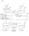
- FIG. 18 shows the operation of the dual-core microcomputer MCU1 according to the first embodiment shown in FIG. 1 by the two CPUs A2 and B6 for the failure detection operation from the parallel data processing by the two CPUs A2 and B6 for the normal operation of the dual-core microcomputer MCU1. It is a figure which shows a mode that it transfers to redundant operation.
- the CPU A2 executes the individual task 200
- the CPU B6 executes the individual task 600
- the task 200 and the task 600 are different tasks.
- the CPU A2 executes a redundant task activation process 201 in order to execute the redundant task 203 for the failure detection operation.
- the activation of the redundant task 603 for the failure detection operation of the CPUB6 can be realized by using, for example, an interrupt process from the CPUA2 to the CPUB6.
- the CPU A2 writes the set value “H0003” in the comparison control register (CCR1) 1611 and supplies the counter reset signal CNTRST and the count enable signal CNTEN to the buffer A11. That is, as shown in FIG. 10, the counter reset of the buffer A11 is executed by the count reset signal CNTRST, and the output data of the CPU A2 is held in the buffer A11 and counted by the count enable signal CNTEN.
- the CPU A2 writes the set value “H0304” in the comparison control register (CCR0) 1610, and sets the set value “1” in the interrupt enable signal INTEN and the comparison enable comparison enable signal CMPEN for the failure detection operation of the comparator 15. The value “1” is set, and the set value “4” is set in the comparison cycle comparison cycle CMPCYC.
- the CPU B 6 receives the interrupt 204 from the CPU A 2 during the execution of the individual task 600 and executes the execution preparation process 602.
- the CPU B6 writes the set value “H0003” in the comparison control register (CCR2) 1612, and supplies the counter reset signal CNTRST and the count enable signal CNTEN to the buffer B12. That is, as shown in FIG. 10, the counter reset of the buffer B12 is executed by the count reset signal CNTRST, and the output data of the CPU B6 is held in the buffer B12 and counted by the count enable signal CNTEN.
- the two CPUs A2 and B6 execute the redundant tasks 203 and 603, respectively, for the failure detection operation. That is, the two CPUs A2 and B6 execute the same redundant task program for the same operand data. Data of a predetermined number of output times selected and output by the two FIFOAs 13 and B14 are compared by the comparator 15. If the comparison results by the comparator 15 match, it is determined that there is no failure in the dual core microcomputer MCU1 of FIG. 1, and if the comparison results by the comparator 15 do not match, the dual core microcomputer MCU1 of FIG. Is determined to have a fault.
- the control unit 16 generates an interrupt request signal 1604 (C_INTREQ) in the interrupt generation circuit 17 in response to the comparison result signal 1500 (CO) of the comparator 15. Therefore, the exception generation circuit 17 notifies that the dual core microcomputer MCU1 according to the first embodiment of the present invention shown in FIG. 1 has failed and one of the two CPUs A2 and B6 is operating abnormally. Is activated in response to an interrupt request signal 1604 (C_INTREQ).
- C_INTREQ interrupt request signal
- the occurrence of a failure of the dual core microcomputer MCU1 is notified by a display device on a dashboard of a driver's seat of an automobile. Therefore, the owner of the automobile can know that the maintenance and repair of the automobile equipped with the dual core microcomputer MCU1 notified of the occurrence of the failure is necessary.
- the transition to the redundant operation by the two CPUs A2 and B6 for the failure detection operation is not limited to the reception of the interrupt 204 described above.
- redundant operation by the two CPUs A2 and B6 for failure detection operation is performed. Is possible. That is, the redundant operation by the two CPUs A2 and B6 is performed, and the parallel data processing of the two CPUs A2 and B6 in the normal operation is started only after it is determined that there is no failure in the dual core microcomputer MCU1.
- a failure detection is performed by periodically issuing a command or interrupt for starting a redundant operation from one of the two CPUs A2 and B6. It is also possible to periodically execute a redundant operation by the two CPUs A2 and B6 for operation. At this time, the contents of the redundant operation executed by the two CPUs A2 and B6 for the failure detection operation are the same as the contents of the data processing of the normal operation executed before one of the two CPUs A2 and B6. Can be done.
- FIG. 19 is a diagram showing another configuration of buffers A11 and B12 as buffer memories according to the second embodiment of the present invention included in dual core microcomputer MCU1 shown in FIG.
- the buffers A11 and B12 as buffer memories according to the second embodiment of the present invention shown in FIG. 19 are different from the buffers A11 and B12 as buffer memories according to the first embodiment of the present invention shown in FIG. Is a point.
- an arithmetic circuit (OP) 1170 not included in the buffer memory according to the first embodiment of the present invention shown in FIG. 2 is added to the buffer memories A11 and B12 according to the second embodiment of the present invention shown in FIG. ing.
- the write data WD and the buffer output signal BO of the flip-flop (FF) 1150 are supplied to one input terminal and the other input terminal of the arithmetic circuit (OP) 1170, respectively.
- the output terminal of (OP) 1170 is connected to the data input terminal of flip-flop (FF) 1150.
- the power-on reset signal RST and the counter reset signal CNR from the control unit 16 are ORed by the OR circuit 1140, and the counter (CNT) 1160 and the flip-flop (FF) are output by the output of the OR circuit 1140. 1150 is reset.
- the arithmetic circuit (OP) 1170 performs arithmetic processing on the write data WD and the buffer output signal BO supplied to one input terminal and the other input terminal, respectively, according to a predetermined arithmetic algorithm.
- An output signal based on the result of the arithmetic processing is generated from the output terminal of the arithmetic circuit (OP) 1170.
- the output signal generated from the output terminal of the arithmetic circuit (OP) 1170 is stored in the flip-flop (FF) 1150 during the period when the buffer write enable signal BWE generated from the output of the AND circuit 1130 is at the high level “1”.
- output signals depending on all values of the plurality of write data WD sequentially supplied from the CPUA2 and CPUB6 are generated from the output terminal of the arithmetic circuit (OP) 1170.
- the arithmetic circuit of the buffer memory A11 is only different in part between the plurality of write data WD sequentially supplied from the CPU A2 to the buffer memory A11 and the plurality of write data WD sequentially supplied from the CPU B6 to the buffer memory B12.
- the output signal generated from the output terminal of (OP) 1170 is different from the output signal generated from the output terminal of operation circuit (OP) 1170 of buffer memory B12.
- the detection probability of abnormality in one of the two CPUs A2 and B6 Can be significantly improved.
- arithmetic algorithm of the arithmetic circuit (OP) 1170 for the values of the plurality of write data WD sequentially supplied to the buffer memories A11 and B12 to affect the value of the buffer output signal BO logical OR or logical
- a relatively simple logical operation such as product AND or exclusive OR EXOR is selected.
- FIG. 20 is a diagram for explaining the operation of buffer memories A11 and B12 with an arithmetic function according to the second embodiment of the present invention shown in FIG.
- the operations of the buffer memories A11 and B12 with arithmetic functions according to the second embodiment of the present invention shown in FIG. 20 are different from the operations of the buffers A11 and B12 according to the first embodiment of the present invention shown in FIG. This is the point.
- the value of the buffer output signal BO of the flip-flop (FF) 1150 is the value of the arithmetic processing (OP) between the initial value BO0 and the data D3 of the write data WD.
- the value of the buffer output signal BO of the flip-flop (FF) 1150 is the arithmetic processing of the previous calculation result value BO1 and the data D4 of the write data WD.
- the value of the buffer output signal BO of the flip-flop (FF) 1150 is the arithmetic processing of the value BO2 of the previous calculation result and the data D8 of the write data WD.
- FIG. 21 is a diagram showing a configuration of a single core microcomputer MCU1 according to the third embodiment of the present invention.
- the single core microcomputer MCU1 according to the third embodiment of the present invention shown in FIG. 21 is different from the dual core microcomputer MCU1 according to the first embodiment of the present invention shown in FIG. 1 in the following points.
- the buffer B12 since the buffer B12 is connected to the CPUA bus 4, the buffer B12 receives data output from the CPUA2 to a specific address space. The number of outputs is held and held.
- a single CPU A2 executes the same redundant task program twice for the same operand data.
- the write data output from the CPU A2 to the specific address space by one operation of the first operation, that is, the double operation is double-written to the memory A3 and the buffer A11.
- the second operation that is, the other operation of the double operation, the write data output from the CPU A2 to the specific address space is double-written to the memory A3 and the buffer B12.
- the two FIFOA 13 and B14 are divided into two buffers A11 and B12 as in the first embodiment of the present invention shown in FIG.
- the CPU A2 selects and stores only a predetermined number of output data from a plurality of data sequentially output and supplied as a redundant task calculation result from the CPU A2, while discarding the other output number data as unselected Is.
- Data of a predetermined number of times of output selected and output by the two FIFOAs 13 and B14 are compared by the comparator 15. If the comparison result by the comparator 15 matches, it is determined that there is no failure in the single core microcomputer MCU1 of FIG. 21, and if the comparison result by the comparator 15 does not match, the single core microcomputer MCU1 of FIG. Is determined to have a fault.
- buffer memories A11, B12 with arithmetic functions according to the second embodiment of the present invention shown in FIGS. 19 and 20 as buffers A11, B12.
- FIG. 22 is a diagram showing a configuration of a triple core microcomputer MCU1 according to the fourth embodiment of the present invention.
- the triple microcomputer MCU1 according to the fourth embodiment of the present invention shown in FIG. 22 is different from the dual core microcomputer MCU1 according to the first embodiment of the present invention shown in FIG. 1 in the following points.
- the triple core microcomputer MCU1 includes a CPU C18 as a third central processing unit, a memory C19 as a third built-in memory, and a CPUC bus 20 as a third CPU bus.
- a bridge C21 as a third bus bridge, a buffer C22 as a third buffer memory, and a FIFOC23 as a third FIFO memory are added.
- the buffer C22 as a third buffer memory is output by the CPU C18 to a specific address space.
- the write data to be held is held and the number of outputs is counted.
- the buffer C22 as the third buffer memory also holds write data that the CPU C18 outputs to a specific address space, and counts the number of outputs.
- the FIFOC 23 as the third FIFO memory holds the output data 2201 of the buffer C22.
- the comparator 15 compares the output data 1300 of the FIFOA 13, the output data 1400 of the FIFOB 14, and the output data 2300 of the FIFO memory.
- the triple core microcomputer MCU1 causes the three CPUs A2, B6, and C18 to execute independent data processing in parallel.
- the results of parallel processing by the three CPUs A2, B6, and C18 can be stored in parallel in the three memories A3, B7, and C19.
- the data in the three memories A3, B7, and C19 can be transferred to the system bus 10 via the three bridges A5, B9, and C21.
- the dual core microcomputer MCU1 according to the fourth embodiment of the present invention shown in FIG. 22 executes the same data processing on the three CPUs A2, B6, and C18, and detects the mismatch of the processing results. Thus, the redundant operation for detecting the failure is executed.
- the three CPUs A2, B6, and C18 execute the same redundant task program for the same operand data.
- the three CPUs A2, B6, and C18 When there is no failure in the triple core microcomputer MCU1 of FIG. 22 and the three CPUs A2, B6, and C18 are operating normally, the three CPUs A2, B6, and C18 output the memory A3 to a specific address space. , B7 and C18 and the write data to be double-written to the buffers A11, B12 and C22 are the same.
- the three CPUs A2, B6, and C18 can move to a specific address space. Write data that is output and double-written in the memories A3, B7, and C18 and the buffers A11, B12, and C22 is inconsistent, and failure detection is possible.
- the three FIFOAs 13, B14, and C23 are predetermined from a plurality of data that are sequentially output and supplied as redundant task calculation results from the three CPUs A2, B6, and C18 via the three buffers A11, B12, and C22. Only the data of the number of output times is selected and stored, while the data of the other number of outputs is discarded as unselected. Data of a predetermined number of output times selected and output by the three FIFO A 13, B 14, and C 23 are compared by the comparator 15. If the comparison result by the comparator 15 matches, it is determined that there is no failure in the triple core microcomputer MCU1 in FIG. 22, and if the comparison result by the comparator 15 does not match, the triple microcomputer MCU1 in FIG.
- the buffers A11, B12, and C22 are provided with the calculation function according to the second embodiment of the present invention shown in FIG. 19 and FIG.
- the memory it is possible to remarkably improve the abnormality detection probability of the single CPU A2.
- FIG. 23 is a diagram showing a configuration of another triple core microcomputer MCU1 according to the fifth embodiment of the present invention.
- the triple microcomputer MCU1 according to the fifth embodiment of the present invention shown in FIG. 23 is different from the triple core microcomputer MCU1 according to the fourth embodiment of the present invention shown in FIG. 22 in the following points.
- the three functional blocks 24, 25, and 26 detect the coincidence / mismatch of the processing results of the three CPUs A2, B6, and C18. It is what I did.
- each of the three functional blocks 24, 25, and 26 included in the triple microcomputer MCU1 according to the fifth embodiment of the present invention shown in FIG. 23 is the same.
- each of the three functional blocks 24, 25, and 26 is controlled by the buffer A11, the buffer B12, the FIFOA 13, the FIFOOB 14, the comparator 15, and the control 15 described in the first embodiment of the present invention shown in FIGS. Part 16.
- the first functional block 24 compares the output data of the first CPU A2 and the output data of the second CPU B6, and outputs an interrupt request 2400 to the interrupt generation circuit 17 if both output data do not match.
- the second functional block 25 compares the output data of the second CPUB 6 and the output data of the third CPUC 18, and can output an interrupt request 2500 to the interrupt generation circuit 17 when both output data do not match. It is.
- the last third function block 26 compares the output data of the first CPU A2 and the output data of the third CPUC 18 and outputs an interrupt request 2600 to the interrupt generation circuit 17 if both output data do not match. Is possible.
- the interrupt generation circuit 17 can accept three interrupt requests from the three functional blocks 24, 25, and 26.
- FIG. 24 shows a dual core microcomputer MCU1 according to the first embodiment of the present invention shown in FIGS. 1 to 18 or a buffer memory A11 with an arithmetic function according to the second embodiment of the present invention shown in FIGS.
- the microcomputer MCU1 is configured to have a function of multiple redundant operations for realizing high reliability.
- the failure of the microcomputer MCU1 can be detected by using the function of multiple redundant operations.
- the calculation result of the microcomputer MCU1 according to the various embodiments of the present invention has high reliability, and therefore an automobile that requires high safety and high accuracy.
- the microcomputer MCU1 can be mounted on
- FIG. 24 shows, as an example, how the microcomputer MCU 1 according to the various embodiments of the present invention described above is mounted inside an electronic control unit (ECU: Electronic Control Unit) 29 that controls the engine 28 of the automobile 27. It is a thing. Therefore, according to the sixth embodiment of the present invention shown in FIG. 24, the control of the engine 28 of the automobile 27 can be made highly reliable and highly accurate.
- ECU Electronic Control Unit
- the present invention is also applicable to a quad-core microcomputer MCU1 having four CPUs. At this time, four buffers and four FIFOs are used, and the output signals of the four FIFOs are supplied to the comparator.
- the present invention is not limited to the multiple redundant operation for detecting the failure of the built-in CPU of the microcontroller.
- the present invention relates to various built-in functional modules of a semiconductor integrated circuit for a wide range of applications, such as a floating point unit (FPU), a number processing unit, a cryptographic processor, an MPEG decoder, a 2D image processor, and a 3D image processor.
- the present invention can be applied to a multiple redundant operation for detecting a failure of a processor or the like.
- the present invention is limited only to the multiple redundant operation for the failure detection operation in the initialization sequence at the time of power-on before the normal operation of the semiconductor integrated circuit and the multiple redundancy operation for the failure detection operation after the start of the normal operation. Is not to be done.
- the multiple redundant operation for the inspection of the semiconductor integrated circuit according to the present invention is, for example, a BIST (Built In Self Test) which is a test for discriminating between good and defective semiconductor chips of the semiconductor integrated circuit at the semiconductor wafer stage before factory shipment. It is possible to apply to.
- the present invention can be widely applied to multiple redundant operations for testing a semiconductor integrated circuit including a functional module and a built-in memory.
- Microcontroller MCU 2 ... 1st central processing unit (CPUA) 3 ... 1st built-in memory (memory A) 4 ... 1st CPU bus (CPUA bus) 5 ... 1st bus bridge (Bridge A) 6 ... Second central processing unit (CPUB) 7 ... Second built-in memory (memory B) 8 ... Second CPU bus (CPUB bus) 9 ... Second bus bridge (Bridge B) 10 ... System bus 11 ... First buffer memory (buffer A) 12 ... Second buffer memory (buffer B) 13: First FIFO memory (FIFOA) 14 ... Second FIFO memory (FIFOB) DESCRIPTION OF SYMBOLS 15 ... Comparator 16 ... Control part 17 ... Interrupt generation circuit
Landscapes
- Engineering & Computer Science (AREA)
- Theoretical Computer Science (AREA)
- Physics & Mathematics (AREA)
- General Engineering & Computer Science (AREA)
- General Physics & Mathematics (AREA)
- Quality & Reliability (AREA)
- Hardware Redundancy (AREA)
Abstract
Description
まず、本願において開示される発明の代表的な実施の形態について概要を説明する。代表的な実施の形態についての概要説明で括弧を付して参照する図面の参照符号は、それが付された構成要素の概念に含まれるものを例示するに過ぎない。
実施の形態について更に詳述する。なお、発明を実施するための形態を説明するための全図において、同一の機能を有する要素には同一の符号を付して、その繰り返しの説明を省略する。
《デュアルコアマイコンの構成》
図1は、本発明の実施の形態1によるデュアルコアマイコンMCU1の構成を示す図である。
図1に示した本発明の実施の形態1によるデュアルコアマイコンMCU1は高性能を実現するために、2個のCPUA2、B6にそれぞれ独立したデータ処理を並列に実行させる。2個のCPUA2、B6による並列処理結果は、2個のメモリA3、B7に並列に格納可能である。更に2個のメモリA3、B7のデータは、2個のブリッジA5、B9を介してシステムバス10に転送されることも可能である。
図1に示した本発明の実施の形態1によるデュアルコアマイコンMCU1は高信頼性を実現するために、2個のCPUA2、B6に同一のデータ処理を実行させその処理結果の不一致を検出して故障を検出するようにした冗長動作が実行される。
図2は、図1に示した本発明の実施の形態1によるデュアルコアマイコンMCU1に含まれるバッファメモリとしてのバッファA11、B12の構成を示す図である。
図3は、本発明の実施の形態1によるデュアルコアマイコンMCU1に含まれる図2に示したバッファメモリとしてのバッファA11、B12の動作を説明する図である。
図4は、図1に示した本発明の実施の形態1によるデュアルコアマイコンMCU1に含まれるFIFOメモリとしてのFIFOA13、B14の構成を示す図である。
図5は、本発明の実施の形態1によるデュアルコアマイコンMCU1に含まれる図4に示したFIFOメモリとしてのFIFOA13、B14の動作を説明する図である。
図6は、図1に示した本発明の実施の形態1によるデュアルコアマイコンMCU1に含まれる比較器15の構成を示す図である。
図7は、本発明の実施の形態1によるデュアルコアマイコンMCU1に含まれる図6に示した比較器15の動作を説明する図である。
図8は、図1に示した本発明の実施の形態1によるデュアルコアマイコンMCU1に含まれる制御部16の構成を示す図である。
図18は、図1に示した本発明の実施の形態1において、デュアルコアマイコンMCU1の通常動作の2個のCPUA2、B6による並列データ処理から故障検出動作のための2個のCPUA2、B6による冗長動作に移行する様子を示す図である。
《バッファメモリの他の構成》
図19は、図1に示すデュアルコアマイコンMCU1に含まれる本発明の実施の形態2によるバッファメモリとしてのバッファA11、B12の他の構成を示す図である。
図20は、図19に示した本発明の実施の形態2による演算機能付きのバッファメモリA11、B12の動作を説明する図である。
《シングルコアマイコンの構成》
図21は、本発明の実施の形態3によるシングルコアマイコンMCU1の構成を示す図である。
《トリプルコアマイコンの構成》
図22は、本発明の実施の形態4によるトリプルコアマイコンMCU1の構成を示す図である。
第3バッファメモリとしてのバッファC22は、CPUC18とが特定のアドレス空間に出力する書き込みデータを保持して、その出力回数をカウントする。第3バッファメモリとしてのバッファC22も、CPUC18が特定のアドレス空間に出力する書き込みデータを保持して、その出力回数をカウントする。第3FIFOメモリとしてのFIFOC23はバッファC22の出力データ2201を保持する。
図22に示した本発明の実施の形態4によるトリプルコアマイコンMCU1は高性能を実現するために、3個のCPUA2、B6、C18にそれぞれ独立したデータ処理を並列に実行させる。3個のCPUA2、B6、C18による並列処理結果は、3個のメモリA3、B7、C19に並列に格納可能である。更に3個のメモリA3、B7、C19のデータは、3個のブリッジA5、B9、C21を介して、システムバス10に転送されることも可能である。
図22に示す本発明の実施の形態4によるデュアルコアマイコンMCU1は高信頼性を実現するために、3個のCPUA2、B6、C18に同一のデータ処理を実行させその処理結果の不一致を検出して故障を検出するようにした冗長動作が実行される。
《他のトリプルコアマイコンの構成》
図23は、本発明の実施の形態5による他のトリプルコアマイコンMCU1の構成を示す図である。
《自動車への高信頼性マイコンの搭載》
図24は、図1乃至図18に示した本発明の実施の形態1によるデュアルコアマイコンMCU1または図19と図20とに示した本発明の実施の形態2による演算機能付きのバッファメモリA11、B12を使用したデュアルコアマイコンMCU1または図21に示した本発明の実施の形態3によるシングルコアマイコンMCU1または図22に示した本発明の実施の形態4によるトリプルマイコンMCU1または図23に示した本発明の実施の形態5によるトリプルマイコンMCU1を搭載した本発明の実施の形態6による自動車の構成を示す図である。
2…第1中央処理ユニット(CPUA)
3…第1内蔵メモリ(メモリA)
4…第1CPUバス(CPUAバス)
5…第1バスブリッジ(ブリッジA)
6…第2中央処理ユニット(CPUB)
7…第2内蔵メモリ(メモリB)
8…第2CPUバス(CPUBバス)
9…第2バスブリッジ(ブリッジB)
10…システムバス
11…第1バッファメモリ(バッファA)
12…第2バッファメモリ(バッファB)
13…第1FIFOメモリ(FIFOA)
14…第2FIFOメモリ(FIFOB)
15…比較器
16…制御部
17…割り込み発生回路
Claims (20)
- 半導体集積回路は、機能モジュールと、内蔵メモリと、第1バッファメモリと、第2バッファメモリと、第1FIFOメモリと、第2FIFOメモリと、比較器とを具備して、
前記半導体集積回路の検査のための多重冗長動作の第1動作の間に前記機能モジュールから出力される第1書き込みデータは前記内蔵メモリと前記第1バッファメモリに供給され、前記半導体集積回路の前記検査のための前記多重冗長動作の第2動作の間に前記機能モジュールから出力される第2書き込みデータは前記内蔵メモリと前記第2バッファメモリに供給され、
前記第1FIFOメモリは前記第1動作の間に前記第1バッファメモリから順次に出力される第1出力データの複数のデータから所定の出力回数のデータを選択して格納する一方、前記所定の出力回数と異なる出力回数の他のデータを非選択として、
前記第2FIFOメモリは前記第2動作の間に前記第2バッファメモリから順次に出力される第2出力データの複数のデータから前記所定の出力回数のデータを選択して格納する一方、前記所定の出力回数と異なる出力回数の他のデータを非選択として、
前記比較器は、前記第1FIFOメモリによって選択され出力される前記所定の出力回数の前記データと前記第2FIFOメモリによって選択され出力される前記所定の出力回数の前記データを比較する
ことを特徴とする半導体集積回路。 - 請求項1において、
前記機能モジュールは、第1機能モジュールと第2機能モジュールとを少なくとも含むものであり、
前記内蔵メモリは、第1内蔵メモリと第2内蔵メモリとを少なくとも含むものであり、
前記第1動作の間に前記第1機能モジュールから出力される前記第1書き込みデータは、前記第1内蔵メモリと前記第1バッファメモリとに供給されるものであり、
前記第2動作の間に前記第2機能モジュールから出力される前記第2書き込みデータは、前記第2内蔵メモリと前記第2バッファメモリとに供給される
ことを特徴とする半導体集積回路。 - 請求項2において、
前記第1機能モジュールと前記第2機能モジュールは、それぞれ第1中央処理ユニットと第2中央処理ユニットである
ことを特徴とする半導体集積回路。 - 請求項2において、
前記第1バッファメモリは、前記第1動作の間に順次に前記第1バッファメモリに供給される前記第1書き込みデータの前記複数のデータの第1出力回数をカウント可能とされ、
前記第2バッファメモリは、前記第2動作の間に順次に前記第2バッファメモリに供給される前記第2書き込みデータの前記複数のデータの第2出力回数をカウント可能とされた
ことを特徴とする半導体集積回路。 - 請求項4において、
前記半導体集積回路は、前記第1バッファメモリと前記第2バッファメモリと前記第1FIFOメモリと前記第2FIFOメモリに接続された制御部を更に具備して、
前記制御部は、前記所定の出力回数の情報を格納可能な第1レジスタと第2レジスタとを含み、
前記第1バッファメモリによってカウントされた前記第1出力回数が前記第1レジスタに格納された前記情報と一致することに応答して、前記第1FIFOメモリが前記所定の出力回数の前記データを選択して格納するための第1FIFOライトイネーブル信号を前記制御部が前記第1FIFOメモリに供給可能とされ、
前記第2バッファメモリによってカウントされた前記第2出力回数が前記第2レジスタに格納された前記情報と一致することに応答して、前記第2FIFOメモリが前記所定の出力回数の前記データを選択して格納するための第2FIFOライトイネーブル信号を前記制御部が前記第2FIFOメモリに供給可能とされた
ことを特徴とする半導体集積回路。 - 請求項3において、
前記多重冗長動作の前記第1動作と前記第2動作の内容は、前記第1中央処理ユニットと前記第2中央処理ユニットとのいずれか一方で以前に実行されていた通常動作の内容とされることが可能である
ことを特徴とする半導体集積回路。 - 請求項6において、
前記通常動作から前記多重冗長動作への移行は、前記通常動作を実行中の前記第1中央処理ユニットと前記第2中央処理ユニットとのいずれか一方から他方への割り込みによって可能とされた
ことを特徴とする半導体集積回路。 - 請求項5において、
前記第1バッファメモリは、前記第1FIFOメモリに出力される前記第1出力データを格納する第1フリップフロップと、一方の入力端子と他方の入力端子とに前記第1書き込みデータと前記第1フリップフロップの出力端子の第1出力データとがそれぞれ供給される第1演算回路とを含み、前記第1演算回路の出力端子から生成される出力信号は前記第1フリップフロップに格納可能とされ、
前記第2バッファメモリは、前記第2FIFOメモリに出力される前記第2出力データを格納する第2フリップフロップと、一方の入力端子と他方の入力端子とに前記第2書き込みデータと前記第2フリップフロップの出力端子の第2出力データとがそれぞれ供給される第2演算回路とを含み、前記第2演算回路の出力端子から生成される出力信号は前記第2フリップフロップに格納可能とされた
ことを特徴とする半導体集積回路。 - 請求項1乃至請求項8のいずれかにおいて、
前記比較器による前記第1FIFOメモリによって出力される前記所定の出力回数の前記データと前記第2FIFOメモリによって出力される前記所定の出力回数の前記データとの比較結果が両方のデータの一致を示す場合には、前記半導体集積回路は正常と判断されて、比較結果が両方のデータの不一致を示す場合には、前記半導体集積回路は異常と判断される
ことを特徴とする半導体集積回路。 - 請求項1乃至請求項8のいずれかにおいて、
前記第1中央処理ユニットは前記第1内蔵メモリに格納された前記通常動作のための命令を実行することに並列して、前記第2中央処理ユニットは前記第12内蔵メモリに格納された前記通常動作のための命令を実行することによって、前記半導体集積回路は多重コアのマイクロコントローラとして動作可能とされた
ことを特徴とする半導体集積回路。 - 半導体集積回路は、機能モジュールと、内蔵メモリと、第1バッファメモリと、第2バッファメモリと、第1FIFOメモリと、第2FIFOメモリと、比較器とを具備して、
前記半導体集積回路の検査のための多重冗長動作の第1動作の間に前記機能モジュールから出力される第1書き込みデータは前記内蔵メモリと前記第1バッファメモリに供給され、前記半導体集積回路の前記検査のための前記多重冗長動作の第2動作の間に前記機能モジュールから出力される第2書き込みデータは前記内蔵メモリと前記第2バッファメモリに供給され、
前記第1FIFOメモリは前記第1動作の間に前記第1バッファメモリから順次に出力される第1出力データの複数のデータから所定の出力回数のデータを選択して格納する一方、前記所定の出力回数と異なる出力回数の他のデータを非選択として、
前記第2FIFOメモリは前記第2動作の間に前記第2バッファメモリから順次に出力される第2出力データの複数のデータから前記所定の出力回数のデータを選択して格納する一方、前記所定の出力回数と異なる出力回数の他のデータを非選択として、
前記比較器は、前記第1FIFOメモリによって選択され出力される前記所定の出力回数の前記データと前記第2FIFOメモリによって選択され出力される前記所定の出力回数の前記データを比較する
ことを特徴とする半導体集積回路の動作方法。 - 請求項11において、
前記機能モジュールは、第1機能モジュールと第2機能モジュールとを少なくとも含むものであり、
前記内蔵メモリは、第1内蔵メモリと第2内蔵メモリとを少なくとも含むものであり、
前記第1動作の間に前記第1機能モジュールから出力される前記第1書き込みデータは、前記第1内蔵メモリと前記第1バッファメモリとに供給されるものであり、
前記第2動作の間に前記第2機能モジュールから出力される前記第2書き込みデータは、前記第2内蔵メモリと前記第2バッファメモリとに供給される
ことを特徴とする半導体集積回路の動作方法。 - 請求項12において、
前記第1機能モジュールと前記第2機能モジュールは、それぞれ第1中央処理ユニットと第2中央処理ユニットである
ことを特徴とする半導体集積回路。 - 請求項12において、
前記第1バッファメモリは、前記第1動作の間に順次に前記第1バッファメモリに供給される前記第1書き込みデータの前記複数のデータの第1出力回数をカウント可能とされ、
前記第2バッファメモリは、前記第2動作の間に順次に前記第2バッファメモリに供給される前記第2書き込みデータの前記複数のデータの第2出力回数をカウント可能とされた
ことを特徴とする半導体集積回路の動作方法。 - 請求項14において、
前記半導体集積回路は、前記第1バッファメモリと前記第2バッファメモリと前記第1FIFOメモリと前記第2FIFOメモリに接続された制御部を更に具備して、
前記制御部は、前記所定の出力回数の情報を格納可能な第1レジスタと第2レジスタとを含み、
前記第1バッファメモリによってカウントされた前記第1出力回数が前記第1レジスタに格納された前記情報と一致することに応答して、前記第1FIFOメモリが前記所定の出力回数の前記データを選択して格納するための第1FIFOライトイネーブル信号を前記制御部が前記第1FIFOメモリに供給可能とされ、
前記第2バッファメモリによってカウントされた前記第2出力回数が前記第2レジスタに格納された前記情報と一致することに応答して、前記第2FIFOメモリが前記所定の出力回数の前記データを選択して格納するための第2FIFOライトイネーブル信号を前記制御部が前記第2FIFOメモリに供給可能とされた
ことを特徴とする半導体集積回路の動作方法。 - 請求項13において、
前記多重冗長動作の前記第1動作と前記第2動作の内容は、前記第1中央処理ユニットと前記第2中央処理ユニットとのいずれか一方で以前に実行されていた通常動作の内容とされることが可能である
ことを特徴とする半導体集積回路の動作方法。 - 請求項16において、
前記通常動作から前記多重冗長動作への移行は、前記通常動作を実行中の前記第1中央処理ユニットと前記第2中央処理ユニットとのいずれか一方から他方への割り込みによって可能とされた
ことを特徴とする半導体集積回路の動作方法。 - 請求項15において、
前記第1バッファメモリは、前記第1FIFOメモリに出力される前記第1出力データを格納する第1フリップフロップと、一方の入力端子と他方の入力端子とに前記第1書き込みデータと前記第1フリップフロップの出力端子の第1出力データとがそれぞれ供給される第1演算回路とを含み、前記第1演算回路の出力端子から生成される出力信号は前記第1フリップフロップに格納可能とされ、
前記第2バッファメモリは、前記第2FIFOメモリに出力される前記第2出力データを格納する第2フリップフロップと、一方の入力端子と他方の入力端子とに前記第2書き込みデータと前記第2フリップフロップの出力端子の第2出力データとがそれぞれ供給される第2演算回路とを含み、前記第2演算回路の出力端子から生成される出力信号は前記第2フリップフロップに格納可能とされた
ことを特徴とする半導体集積回路の動作方法。 - 請求項11乃至請求項18のいずれかにおいて、
前記比較器による前記第1FIFOメモリによって出力される前記所定の出力回数の前記データと前記第2FIFOメモリによって出力される前記所定の出力回数の前記データとの比較結果が両方のデータの一致を示す場合には、前記半導体集積回路は正常と判断されて、比較結果が両方のデータの不一致を示す場合には、前記半導体集積回路は異常と判断される
ことを特徴とする半導体集積回路の動作方法。 - 請求項11乃至請求項18のいずれかにおいて、
前記第1中央処理ユニットは前記第1内蔵メモリに格納された前記通常動作のための命令を実行することに並列して、前記第2中央処理ユニットは前記第12内蔵メモリに格納された前記通常動作のための命令を実行することによって、前記半導体集積回路は多重コアのマイクロコントローラとして動作可能とされた
ことを特徴とする半導体集積回路の動作方法。
Priority Applications (3)
| Application Number | Priority Date | Filing Date | Title |
|---|---|---|---|
| US14/110,786 US9367438B2 (en) | 2011-04-21 | 2011-04-21 | Semiconductor integrated circuit and method for operating same |
| PCT/JP2011/059807 WO2012144043A1 (ja) | 2011-04-21 | 2011-04-21 | 半導体集積回路とその動作方法 |
| JP2013510786A JP5693712B2 (ja) | 2011-04-21 | 2011-04-21 | 半導体集積回路 |
Applications Claiming Priority (1)
| Application Number | Priority Date | Filing Date | Title |
|---|---|---|---|
| PCT/JP2011/059807 WO2012144043A1 (ja) | 2011-04-21 | 2011-04-21 | 半導体集積回路とその動作方法 |
Publications (1)
| Publication Number | Publication Date |
|---|---|
| WO2012144043A1 true WO2012144043A1 (ja) | 2012-10-26 |
Family
ID=47041192
Family Applications (1)
| Application Number | Title | Priority Date | Filing Date |
|---|---|---|---|
| PCT/JP2011/059807 Ceased WO2012144043A1 (ja) | 2011-04-21 | 2011-04-21 | 半導体集積回路とその動作方法 |
Country Status (3)
| Country | Link |
|---|---|
| US (1) | US9367438B2 (ja) |
| JP (1) | JP5693712B2 (ja) |
| WO (1) | WO2012144043A1 (ja) |
Families Citing this family (26)
| Publication number | Priority date | Publication date | Assignee | Title |
|---|---|---|---|---|
| US10157060B2 (en) | 2011-12-29 | 2018-12-18 | Intel Corporation | Method, device and system for control signaling in a data path module of a data stream processing engine |
| US10331583B2 (en) | 2013-09-26 | 2019-06-25 | Intel Corporation | Executing distributed memory operations using processing elements connected by distributed channels |
| KR101764680B1 (ko) * | 2014-12-29 | 2017-08-03 | 주식회사 효성 | 이중화 제어 시스템 |
| EP4557209A3 (en) * | 2015-06-10 | 2025-08-13 | Mobileye Vision Technologies Ltd. | Image processor and methods for processing an image |
| US9966124B2 (en) | 2016-09-02 | 2018-05-08 | Toshiba Memory Corporation | Memory device |
| US10558575B2 (en) | 2016-12-30 | 2020-02-11 | Intel Corporation | Processors, methods, and systems with a configurable spatial accelerator |
| US10515046B2 (en) | 2017-07-01 | 2019-12-24 | Intel Corporation | Processors, methods, and systems with a configurable spatial accelerator |
| US10515049B1 (en) | 2017-07-01 | 2019-12-24 | Intel Corporation | Memory circuits and methods for distributed memory hazard detection and error recovery |
| JP2019053600A (ja) * | 2017-09-15 | 2019-04-04 | ルネサスエレクトロニクス株式会社 | 半導体集積回路装置及びデータ比較方法 |
| US11086816B2 (en) | 2017-09-28 | 2021-08-10 | Intel Corporation | Processors, methods, and systems for debugging a configurable spatial accelerator |
| US10496574B2 (en) | 2017-09-28 | 2019-12-03 | Intel Corporation | Processors, methods, and systems for a memory fence in a configurable spatial accelerator |
| US10564980B2 (en) | 2018-04-03 | 2020-02-18 | Intel Corporation | Apparatus, methods, and systems for conditional queues in a configurable spatial accelerator |
| US11307873B2 (en) | 2018-04-03 | 2022-04-19 | Intel Corporation | Apparatus, methods, and systems for unstructured data flow in a configurable spatial accelerator with predicate propagation and merging |
| US20190349147A1 (en) * | 2018-05-10 | 2019-11-14 | Sharp Laboratories Of America, Inc. | User equipments, base stations and methods for uplink control information multiplexing in uplink |
| US10459866B1 (en) * | 2018-06-30 | 2019-10-29 | Intel Corporation | Apparatuses, methods, and systems for integrated control and data processing in a configurable spatial accelerator |
| US10891240B2 (en) | 2018-06-30 | 2021-01-12 | Intel Corporation | Apparatus, methods, and systems for low latency communication in a configurable spatial accelerator |
| US11200186B2 (en) | 2018-06-30 | 2021-12-14 | Intel Corporation | Apparatuses, methods, and systems for operations in a configurable spatial accelerator |
| US10678724B1 (en) | 2018-12-29 | 2020-06-09 | Intel Corporation | Apparatuses, methods, and systems for in-network storage in a configurable spatial accelerator |
| US10915471B2 (en) | 2019-03-30 | 2021-02-09 | Intel Corporation | Apparatuses, methods, and systems for memory interface circuit allocation in a configurable spatial accelerator |
| US10965536B2 (en) | 2019-03-30 | 2021-03-30 | Intel Corporation | Methods and apparatus to insert buffers in a dataflow graph |
| US10817291B2 (en) | 2019-03-30 | 2020-10-27 | Intel Corporation | Apparatuses, methods, and systems for swizzle operations in a configurable spatial accelerator |
| US11029927B2 (en) | 2019-03-30 | 2021-06-08 | Intel Corporation | Methods and apparatus to detect and annotate backedges in a dataflow graph |
| US11037050B2 (en) | 2019-06-29 | 2021-06-15 | Intel Corporation | Apparatuses, methods, and systems for memory interface circuit arbitration in a configurable spatial accelerator |
| US11907713B2 (en) | 2019-12-28 | 2024-02-20 | Intel Corporation | Apparatuses, methods, and systems for fused operations using sign modification in a processing element of a configurable spatial accelerator |
| US12086080B2 (en) | 2020-09-26 | 2024-09-10 | Intel Corporation | Apparatuses, methods, and systems for a configurable accelerator having dataflow execution circuits |
| US11625198B1 (en) * | 2022-04-02 | 2023-04-11 | Changxin Memory Technologies, Inc. | Detection circuit, detection method and memory device |
Citations (6)
| Publication number | Priority date | Publication date | Assignee | Title |
|---|---|---|---|---|
| JPH04138532A (ja) * | 1990-09-28 | 1992-05-13 | Nec Corp | 暴走検出回路 |
| JPH07146802A (ja) * | 1993-11-24 | 1995-06-06 | Kyosan Electric Mfg Co Ltd | 鉄道保安装置 |
| JPH08241217A (ja) * | 1995-03-07 | 1996-09-17 | Hitachi Ltd | 情報処理装置 |
| JP2004234144A (ja) * | 2003-01-29 | 2004-08-19 | Hitachi Ltd | プロセッサの動作比較装置および動作比較方法 |
| JP2007507015A (ja) * | 2003-06-24 | 2007-03-22 | ローベルト ボッシュ ゲゼルシャフト ミット ベシュレンクテル ハフツング | プロセッサユニットの少なくとも2つの動作モードを切替る方法および対応するプロセッサユニット |
| JP2010113388A (ja) * | 2008-11-04 | 2010-05-20 | Renesas Technology Corp | 処理結果を照合する比較器を有するマルチコアマイコン |
Family Cites Families (8)
| Publication number | Priority date | Publication date | Assignee | Title |
|---|---|---|---|---|
| JPH06324900A (ja) | 1993-05-10 | 1994-11-25 | Mitsubishi Electric Corp | 計算機 |
| JPH10261762A (ja) | 1997-03-19 | 1998-09-29 | Hitachi Ltd | メモリを内蔵した多重化マイクロコントローラ |
| US6289022B1 (en) * | 1997-10-21 | 2001-09-11 | The Foxboro Company | Methods and systems for fault-tolerant data transmission |
| US6820213B1 (en) * | 2000-04-13 | 2004-11-16 | Stratus Technologies Bermuda, Ltd. | Fault-tolerant computer system with voter delay buffer |
| US6799285B2 (en) * | 2001-03-19 | 2004-09-28 | Sun Microsystems, Inc. | Self-checking multi-threaded processor |
| GB2473674A (en) * | 2009-09-22 | 2011-03-23 | Sony Corp | OFDM receiver with a plurality of prediction filters to reduce noise in channel transfer function estimates |
| US9047178B2 (en) * | 2010-12-13 | 2015-06-02 | SanDisk Technologies, Inc. | Auto-commit memory synchronization |
| US9208071B2 (en) * | 2010-12-13 | 2015-12-08 | SanDisk Technologies, Inc. | Apparatus, system, and method for accessing memory |
-
2011
- 2011-04-21 US US14/110,786 patent/US9367438B2/en not_active Expired - Fee Related
- 2011-04-21 WO PCT/JP2011/059807 patent/WO2012144043A1/ja not_active Ceased
- 2011-04-21 JP JP2013510786A patent/JP5693712B2/ja not_active Expired - Fee Related
Patent Citations (6)
| Publication number | Priority date | Publication date | Assignee | Title |
|---|---|---|---|---|
| JPH04138532A (ja) * | 1990-09-28 | 1992-05-13 | Nec Corp | 暴走検出回路 |
| JPH07146802A (ja) * | 1993-11-24 | 1995-06-06 | Kyosan Electric Mfg Co Ltd | 鉄道保安装置 |
| JPH08241217A (ja) * | 1995-03-07 | 1996-09-17 | Hitachi Ltd | 情報処理装置 |
| JP2004234144A (ja) * | 2003-01-29 | 2004-08-19 | Hitachi Ltd | プロセッサの動作比較装置および動作比較方法 |
| JP2007507015A (ja) * | 2003-06-24 | 2007-03-22 | ローベルト ボッシュ ゲゼルシャフト ミット ベシュレンクテル ハフツング | プロセッサユニットの少なくとも2つの動作モードを切替る方法および対応するプロセッサユニット |
| JP2010113388A (ja) * | 2008-11-04 | 2010-05-20 | Renesas Technology Corp | 処理結果を照合する比較器を有するマルチコアマイコン |
Also Published As
| Publication number | Publication date |
|---|---|
| US9367438B2 (en) | 2016-06-14 |
| JPWO2012144043A1 (ja) | 2014-07-28 |
| JP5693712B2 (ja) | 2015-04-01 |
| US20140032860A1 (en) | 2014-01-30 |
Similar Documents
| Publication | Publication Date | Title |
|---|---|---|
| JP5693712B2 (ja) | 半導体集積回路 | |
| JP5507830B2 (ja) | マイクロコントローラ及び自動車制御装置 | |
| JP5850774B2 (ja) | 半導体集積回路装置及びそれを用いたシステム | |
| TWI651652B (zh) | 汽車用的控制裝置 | |
| CN104765650A (zh) | 数据处理装置 | |
| US9665466B2 (en) | Debug architecture for multithreaded processors | |
| JP2011513843A (ja) | 実行装置内のデータ転送のシステムおよび方法 | |
| JP2014063258A (ja) | 半導体集積回路装置及びマイクロコントローラ | |
| US8639905B2 (en) | Microcontroller and electronic control unit | |
| US10102166B2 (en) | Multiprocessor system | |
| US8621273B2 (en) | Enhanced scalable CPU for coded execution of SW in high-dependable safety relevant applications | |
| US20150046759A1 (en) | Semiconductor integrated circuit device | |
| CN108369519B (zh) | 在使用块-原子执行模型的基于处理器的系统中重放部分执行的指令块 | |
| US9785538B2 (en) | Arbitrary instruction execution from context memory | |
| JP2018112977A (ja) | マイクロコンピュータ | |
| US9305614B2 (en) | Memory device with internal combination logic | |
| US20160055001A1 (en) | Low power instruction buffer for high performance processors | |
| US20260003727A1 (en) | Scalable architecture for configurable dynamic error correction coding (ecc) memory | |
| JP2013030056A (ja) | 半導体集積回路装置 | |
| CN116361233A (zh) | 一种微控制器 |
Legal Events
| Date | Code | Title | Description |
|---|---|---|---|
| 121 | Ep: the epo has been informed by wipo that ep was designated in this application |
Ref document number: 11864085 Country of ref document: EP Kind code of ref document: A1 |
|
| ENP | Entry into the national phase |
Ref document number: 2013510786 Country of ref document: JP Kind code of ref document: A |
|
| WWE | Wipo information: entry into national phase |
Ref document number: 14110786 Country of ref document: US |
|
| NENP | Non-entry into the national phase |
Ref country code: DE |
|
| 122 | Ep: pct application non-entry in european phase |
Ref document number: 11864085 Country of ref document: EP Kind code of ref document: A1 |