WO2012141141A1 - 太陽電池、太陽電池パネルおよび太陽電池を備えた装置 - Google Patents
太陽電池、太陽電池パネルおよび太陽電池を備えた装置 Download PDFInfo
- Publication number
- WO2012141141A1 WO2012141141A1 PCT/JP2012/059704 JP2012059704W WO2012141141A1 WO 2012141141 A1 WO2012141141 A1 WO 2012141141A1 JP 2012059704 W JP2012059704 W JP 2012059704W WO 2012141141 A1 WO2012141141 A1 WO 2012141141A1
- Authority
- WO
- WIPO (PCT)
- Prior art keywords
- photoelectric conversion
- conversion layer
- solar cell
- photonic crystal
- transparent conductive
- Prior art date
- Legal status (The legal status is an assumption and is not a legal conclusion. Google has not performed a legal analysis and makes no representation as to the accuracy of the status listed.)
- Ceased
Links
Images











Classifications
-
- G—PHYSICS
- G02—OPTICS
- G02B—OPTICAL ELEMENTS, SYSTEMS OR APPARATUS
- G02B1/00—Optical elements characterised by the material of which they are made; Optical coatings for optical elements
- G02B1/002—Optical elements characterised by the material of which they are made; Optical coatings for optical elements made of materials engineered to provide properties not available in nature, e.g. metamaterials
- G02B1/005—Optical elements characterised by the material of which they are made; Optical coatings for optical elements made of materials engineered to provide properties not available in nature, e.g. metamaterials made of photonic crystals or photonic band gap materials
-
- H—ELECTRICITY
- H10—SEMICONDUCTOR DEVICES; ELECTRIC SOLID-STATE DEVICES NOT OTHERWISE PROVIDED FOR
- H10F—INORGANIC SEMICONDUCTOR DEVICES SENSITIVE TO INFRARED RADIATION, LIGHT, ELECTROMAGNETIC RADIATION OF SHORTER WAVELENGTH OR CORPUSCULAR RADIATION
- H10F10/00—Individual photovoltaic cells, e.g. solar cells
- H10F10/10—Individual photovoltaic cells, e.g. solar cells having potential barriers
- H10F10/17—Photovoltaic cells having only PIN junction potential barriers
- H10F10/172—Photovoltaic cells having only PIN junction potential barriers comprising multiple PIN junctions, e.g. tandem cells
-
- H—ELECTRICITY
- H10—SEMICONDUCTOR DEVICES; ELECTRIC SOLID-STATE DEVICES NOT OTHERWISE PROVIDED FOR
- H10F—INORGANIC SEMICONDUCTOR DEVICES SENSITIVE TO INFRARED RADIATION, LIGHT, ELECTROMAGNETIC RADIATION OF SHORTER WAVELENGTH OR CORPUSCULAR RADIATION
- H10F10/00—Individual photovoltaic cells, e.g. solar cells
- H10F10/10—Individual photovoltaic cells, e.g. solar cells having potential barriers
- H10F10/17—Photovoltaic cells having only PIN junction potential barriers
- H10F10/174—Photovoltaic cells having only PIN junction potential barriers comprising monocrystalline or polycrystalline materials
-
- H—ELECTRICITY
- H10—SEMICONDUCTOR DEVICES; ELECTRIC SOLID-STATE DEVICES NOT OTHERWISE PROVIDED FOR
- H10F—INORGANIC SEMICONDUCTOR DEVICES SENSITIVE TO INFRARED RADIATION, LIGHT, ELECTROMAGNETIC RADIATION OF SHORTER WAVELENGTH OR CORPUSCULAR RADIATION
- H10F77/00—Constructional details of devices covered by this subclass
- H10F77/10—Semiconductor bodies
- H10F77/14—Shape of semiconductor bodies; Shapes, relative sizes or dispositions of semiconductor regions within semiconductor bodies
- H10F77/147—Shapes of bodies
-
- H—ELECTRICITY
- H10—SEMICONDUCTOR DEVICES; ELECTRIC SOLID-STATE DEVICES NOT OTHERWISE PROVIDED FOR
- H10F—INORGANIC SEMICONDUCTOR DEVICES SENSITIVE TO INFRARED RADIATION, LIGHT, ELECTROMAGNETIC RADIATION OF SHORTER WAVELENGTH OR CORPUSCULAR RADIATION
- H10F77/00—Constructional details of devices covered by this subclass
- H10F77/30—Coatings
- H10F77/306—Coatings for devices having potential barriers
- H10F77/311—Coatings for devices having potential barriers for photovoltaic cells
- H10F77/315—Coatings for devices having potential barriers for photovoltaic cells the coatings being antireflective or having enhancing optical properties
-
- H—ELECTRICITY
- H10—SEMICONDUCTOR DEVICES; ELECTRIC SOLID-STATE DEVICES NOT OTHERWISE PROVIDED FOR
- H10F—INORGANIC SEMICONDUCTOR DEVICES SENSITIVE TO INFRARED RADIATION, LIGHT, ELECTROMAGNETIC RADIATION OF SHORTER WAVELENGTH OR CORPUSCULAR RADIATION
- H10F77/00—Constructional details of devices covered by this subclass
- H10F77/40—Optical elements or arrangements
- H10F77/42—Optical elements or arrangements directly associated or integrated with photovoltaic cells, e.g. light-reflecting means or light-concentrating means
- H10F77/48—Back surface reflectors [BSR]
-
- Y—GENERAL TAGGING OF NEW TECHNOLOGICAL DEVELOPMENTS; GENERAL TAGGING OF CROSS-SECTIONAL TECHNOLOGIES SPANNING OVER SEVERAL SECTIONS OF THE IPC; TECHNICAL SUBJECTS COVERED BY FORMER USPC CROSS-REFERENCE ART COLLECTIONS [XRACs] AND DIGESTS
- Y02—TECHNOLOGIES OR APPLICATIONS FOR MITIGATION OR ADAPTATION AGAINST CLIMATE CHANGE
- Y02E—REDUCTION OF GREENHOUSE GAS [GHG] EMISSIONS, RELATED TO ENERGY GENERATION, TRANSMISSION OR DISTRIBUTION
- Y02E10/00—Energy generation through renewable energy sources
- Y02E10/50—Photovoltaic [PV] energy
- Y02E10/52—PV systems with concentrators
-
- Y—GENERAL TAGGING OF NEW TECHNOLOGICAL DEVELOPMENTS; GENERAL TAGGING OF CROSS-SECTIONAL TECHNOLOGIES SPANNING OVER SEVERAL SECTIONS OF THE IPC; TECHNICAL SUBJECTS COVERED BY FORMER USPC CROSS-REFERENCE ART COLLECTIONS [XRACs] AND DIGESTS
- Y02—TECHNOLOGIES OR APPLICATIONS FOR MITIGATION OR ADAPTATION AGAINST CLIMATE CHANGE
- Y02E—REDUCTION OF GREENHOUSE GAS [GHG] EMISSIONS, RELATED TO ENERGY GENERATION, TRANSMISSION OR DISTRIBUTION
- Y02E10/00—Energy generation through renewable energy sources
- Y02E10/50—Photovoltaic [PV] energy
- Y02E10/547—Monocrystalline silicon PV cells
-
- Y—GENERAL TAGGING OF NEW TECHNOLOGICAL DEVELOPMENTS; GENERAL TAGGING OF CROSS-SECTIONAL TECHNOLOGIES SPANNING OVER SEVERAL SECTIONS OF THE IPC; TECHNICAL SUBJECTS COVERED BY FORMER USPC CROSS-REFERENCE ART COLLECTIONS [XRACs] AND DIGESTS
- Y02—TECHNOLOGIES OR APPLICATIONS FOR MITIGATION OR ADAPTATION AGAINST CLIMATE CHANGE
- Y02E—REDUCTION OF GREENHOUSE GAS [GHG] EMISSIONS, RELATED TO ENERGY GENERATION, TRANSMISSION OR DISTRIBUTION
- Y02E10/00—Energy generation through renewable energy sources
- Y02E10/50—Photovoltaic [PV] energy
- Y02E10/548—Amorphous silicon PV cells
Definitions
- the present invention relates to a tandem solar cell, a solar cell panel in which a plurality of the solar cells are arranged, and a device in which the solar cell is mounted as a power source.
- a tandem film is formed by stacking a photoelectric conversion layer using amorphous silicon (a-Si) as a medium and a photoelectric conversion layer using microcrystalline silicon ( ⁇ c-Si) as a medium to form a two-layer film.
- a-Si amorphous silicon
- ⁇ c-Si microcrystalline silicon
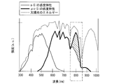
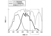
- FIG. 22 shows the relationship between the energy of sunlight at each wavelength and the sensitivity characteristics of the photoelectric conversion layer in a conventionally used tandem solar cell.
- FIG. 22 is a graph showing the relationship between the energy at each wavelength of sunlight and the sensitivity characteristics of the photoelectric conversion layer.
- the 22 indicates the intensity of energy at each wavelength of sunlight (hereinafter also simply referred to as light energy).
- the thin line indicates the sensitivity characteristic of the a-Si photoelectric conversion layer using amorphous silicon as the medium of the photoelectric conversion layer, that is, the intensity of light absorption.
- the thick line indicates that microcrystalline silicon is used as the medium of the photoelectric conversion layer.
- the sensitivity characteristic of the ⁇ c-Si photoelectric conversion layer, that is, the intensity of light absorption is shown.
- the a-Si photoelectric conversion layer absorbs light in the wavelength range of about 700 nm or less, and the intensity of light absorption increases particularly in the vicinity of the wavelength of about 500 nm.
- the ⁇ c-Si photoelectric conversion layer has light absorption in the wavelength range of about 450 nm to about 950 nm, and particularly, the light absorption intensity increases in the wavelength range of about 600 nm to about 700 nm.
- the two layers complement light absorption efficiency in a wavelength range of about 750 nm or less. So that it can absorb light efficiently.
- Patent Document 1 discloses a technique for receiving sunlight more efficiently and supplying it to a solar cell.
- FIG. 23 sectional drawing showing the outline
- the solar cell according to Patent Document 1 is made of a transparent material called a dielectric antenna provided on the surface of the solar cell (regardless of organic or inorganic, for example, polyethylene and SiO2) in a rod shape.
- a dielectric antenna provided on the surface of the solar cell (regardless of organic or inorganic, for example, polyethylene and SiO2) in a rod shape.
- the amount of external light is increased by causing interaction with light. This increases the electromotive force by capturing light that cannot be captured due to surface reflection.
- the solar cell disclosed in Patent Document 1 has the following problems. Although the solar cell described in Patent Document 1 increases the amount of light to be captured, it does not improve the light absorptance on the long wavelength side where light absorption is small, so the light absorptance on the long wavelength side is still high. There is a problem that it is low.
- the solar cell described in Patent Document 1 can take in more incident light from various angles than usual by using a dielectric antenna, thereby reducing the amount of light absorbed by the entire solar cell. It is improving.
- the solar cell described in Patent Document 1 since the captured light cannot be confined in the solar cell, even though the light can be efficiently captured, the captured light cannot be efficiently absorbed. . Therefore, there is a problem that a lot of light that is not absorbed among the taken-in light exists in the solar cell, and the light absorption rate cannot be improved efficiently.
- the present invention has been made in view of the above problems, and an object of the present invention is to provide a solar cell having an increased light absorption rate particularly at a long wavelength.
- a solar cell mainly absorbs a short-wavelength light and photoelectrically converts the first photoelectric conversion layer, and mainly absorbs a long-wavelength light.
- a second photoelectric conversion layer that performs photoelectric conversion and a plurality of columnar media, and the second photoelectric conversion layer is formed to cover the plurality of columnar media from the side opposite to the light incident side;
- a first photonic crystal is formed together with the plurality of columnar media.
- the solar cell absorbs light on the short wavelength side in the first photoelectric conversion layer, and absorbs light on the long wavelength in the second photoelectric conversion layer. For this reason, light of a wide range of wavelengths can be absorbed.
- the first photonic crystal having a refractive index difference is constituted by the second photoelectric conversion layer and the plurality of columnar media, so that the light taken into the solar cell can be captured. It can resonate (resonance effect). Further, the sun leaks from the light leaking from the first photonic crystal and the light that passes through the second conversion layer and is incident again from the surface opposite to the light incident side of the second conversion layer. The light taken into the battery can interfere with each other (interference effect).
- the solar cell can confine the captured light by the resonance effect and the interference effect of the first photonic crystal.
- the path of light passing through the second photoelectric conversion layer can be increased. Therefore (diffraction scattering effect), the light absorption rate can be increased.
- the solar cell is formed so that the second photoelectric conversion layer covers the plurality of columnar media.
- the second photoelectric conversion layer is embedded in the plurality of columnar media so as not to perform processing that damages the second photoelectric conversion layer.
- a first photonic crystal can be formed.
- the solar cell can efficiently increase the light absorption rate in the second photoelectric conversion layer, particularly the light absorption rate at a long wavelength, and improve the photoelectric conversion rate.
- the amount of electromotive force in the solar cell Can be increased.
- a solar cell panel includes a plurality of units arranged one-dimensionally or two-dimensionally, with a solar cell as one unit. Yes.
- a solar cell in which no defect is provided in the first photonic crystal is easier to manufacture than a solar cell in which a defect is provided in the first photonic crystal. Therefore, the solar cell panel in which the solar cells not provided with defects in the first photonic crystal are arranged has an advantage of being suitable for mass production.
- An apparatus provided with any of the above solar cells as a power source is also one category of the present invention.
- Such devices include portable or stationary electronic devices, home appliances, advertising towers, and the like that operate using the solar cell as a power source.
- the apparatus provided with the said solar cell panel as a power supply is also one category of this invention.
- Such devices include vehicles or advertising towers in addition to portable or stationary electronic devices or home appliances that operate using the solar cell panel as a power source.
- the solar cell according to one embodiment of the present invention mainly absorbs a short wavelength light and photoelectrically converts the first photoelectric conversion layer, and mainly absorbs a long wavelength light and performs a photoelectric conversion.
- 2 photoelectric conversion layers and a first photonic crystal, and the second photoelectric conversion layer is formed so as to cover the first photonic crystal.
- the solar cell can efficiently increase the light absorption rate in the second photoelectric conversion layer, particularly the light absorption rate at a long wavelength, and improve the photoelectric conversion rate.
- FIG. 5 is a graph showing the intensity of light resonance with respect to a normalized frequency when an electromagnetic field analysis using a finite element method is performed on the first photonic crystal structure of a solar cell according to an embodiment of the present invention. is there.
- the relationship between the energy at each wavelength of sunlight and the sensitivity characteristic of the photoelectric conversion layer when the first photonic crystal is designed to improve the light absorption rate. It is a graph to show. It is process drawing which shows the manufacturing process of the solar cell which concerns on one Embodiment of this invention. It is a top view which shows typically the structure of the 1st photonic crystal in the solar cell which concerns on other embodiment of this invention. In the solar cell concerning other embodiments of the present invention, it is a top view showing typically the structure of the 1st photonic crystal at the time of forming a defect in the 1st photonic crystal.
- the solar cell which concerns on other embodiment of this invention, it is a figure which shows distribution of the strength of the resonance in a 1st photonic crystal when not forming a defect. It is a figure which shows distribution of the intensity of resonance in the 1st photonic crystal at the time of forming a defect in the solar cell concerning other embodiments of the present invention.
- the energy at each wavelength of sunlight and the sensitivity characteristics of the photoelectric conversion layer when the first photonic crystal is configured by arranging the nanorods in a triangular lattice shape It is a graph which shows the relationship. It is sectional drawing which shows roughly the whole structure of the solar cell which concerns on further another embodiment of this invention.
- the top view which shows typically the structure of the photonic crystal arrange
- a structure of a photonic crystal in which two types of nanorods having different radii are arranged so as to form two types of square lattice structures having different sizes is schematically illustrated.
- FIG. It is a graph which shows the relationship between the energy of sunlight in each wavelength, and the sensitivity characteristic of a photoelectric converting layer.
- 10 is a cross-sectional view illustrating an outline of a solar cell according to Patent Document 1.
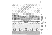
- FIG. 1 is a cross-sectional view schematically showing the overall configuration of the solar cell 1 of the present embodiment.
- the solar cell 1 can be used by converting incident light into electric current by photoelectric conversion.
- the solar cell 1 includes a first photoelectric conversion layer 11, a second photoelectric conversion layer 12, an intermediate transparent conductive film (first transparent conductive film) 13, and a transparent conductive film (second transparent conductive film) 14.
- a transparent conductive film 15 (third transparent conductive film), a transparent substrate 16, and a metal electrode 17.
- the second photoelectric conversion layer 12 has a first photonic crystal structure in which nanorods (columnar media) 20 are periodically arranged. More specifically, the second photoelectric conversion layer 12 is formed so as to cover the plurality of nanorods 20 from the side opposite to the light incident side, thereby forming a first photonic crystal together with the plurality of nanorods 20. ing.
- the first photoelectric conversion layer 11 is a semiconductor layer that mainly absorbs light of a short wavelength and performs photoelectric conversion.
- the first photoelectric conversion layer 11 has a structure in which semiconductor layers having different polarities are adjacent to each other, and the structure is not particularly limited.
- an i-type semiconductor layer (so-called intrinsic semiconductor layer) 112 is formed as a p-type.
- a pin vertical structure sandwiched between the semiconductor layer 111 and the n-type semiconductor layer 113 may be employed.
- Examples of the medium of the first photoelectric conversion layer 11 include amorphous silicon (a-Si) having a refractive index of about 3.0 to 4.0, but are not limited thereto.
- Si, Ge, GaNINGaP, (In) GeAs, GaAs, or the like may be used.
- the second photoelectric conversion layer 12 is a semiconductor layer that mainly performs photoelectric conversion by absorbing long-wavelength light.
- the second photoelectric conversion layer 12 has a structure in which semiconductor layers having different polarities are adjacent to each other.
- the i-type semiconductor layer 122 is replaced with the p-type semiconductor layer 121 and the n-type semiconductor layer 121.
- a pin vertical structure sandwiched between the semiconductor layers 123 may be employed.
- the medium of the second photoelectric conversion layer 12 include microcrystalline silicon ( ⁇ c-Si) having a refractive index of about 3.0 to 4.0, but are not limited thereto. Absent.
- polysilicon p-Si: high-purity polycrystalline silicon
- the p-type semiconductor layer 121 of the second photoelectric conversion layer 12 is formed so as to cover the first photonic crystal in which the nanorods 20 are periodically arranged. The nanorod 20 and the first photonic crystal will be described later.
- the intermediate transparent conductive film 13 is a transparent conductive film, and is disposed so as to be sandwiched between the first photoelectric conversion layer 11 and the second photoelectric conversion layer 12.
- transparent conductive films (TCO; Transparent Conducting Oxide) 14 and 15 are transparent conductive films, and are disposed with the first photoelectric conversion layer 11 and the second photoelectric conversion layer 12 interposed therebetween.
- the intermediate transparent conductive film 13 is flattened so that either one of the first photoelectric conversion layer 11 side and the second photoelectric conversion layer 12 side is flat.
- the first photoelectric conversion layer 11 side or the second photoelectric conversion layer 12 side of the intermediate transparent conductive film 13 is selected. Can be made flat. That is, by increasing the thickness of the intermediate transparent conductive film 13, the planarization process can be omitted.
- the intermediate transparent conductive film 13 and the transparent conductive films 14 and 15 are made of a medium having a refractive index smaller than that of the medium of the first photoelectric conversion layer 11 and the second photoelectric conversion layer 12.
- the medium for example, ITO (Indium) -Tin-Oxide), ZnO, SnO2 and the like.
- the transparent conductive film 14 is disposed on the transparent substrate 16 side with the first photoelectric conversion layer 11 and the second photoelectric conversion layer 12 interposed between the transparent conductive film 15 and the transparent conductive film 15.
- the first photoelectric conversion layer 11 and the second photoelectric conversion layer 12 are interposed between and the metal electrode 17 side.
- the transparent substrate 16 for example, glass having a refractive index of about 1.52 can be selected.
- the material of the metal electrode 17 a material having high light reflectivity and high electrical conductivity, for example, Ag or Al can be selected.
- the light incident on the first photoelectric conversion layer 11 and the second photoelectric conversion layer 12 through the transparent substrate 16 generates electrons and holes mainly in the i-type semiconductor layers 112 and 122, and converts the electrons into valence electrons. It is absorbed by excitation from the band to the conduction band.
- the metal electrode 17 can also function as a reflector, and light that has not been photoelectrically converted by the first photoelectric conversion layer 11 and the second photoelectric conversion layer 12 and has been transmitted through the first photoelectric conversion layer 11 and the second photoelectric conversion layer 11 again. It can also be reflected to the second photoelectric conversion layer 12.
- the metal electrode 17 By disposing the metal electrode 17 so as to cover the entire back surface of the solar cell 1, the light transmitted through the first photoelectric conversion layer 11 and the second photoelectric conversion layer 12 can be reliably reflected.
- the solar cell 1 with high absorption efficiency can be configured.
- FIG. 2 is a top view of the first photonic crystal structure when the nanorods 20 constituting the first photonic crystal are cylindrical.
- FIG. 3 is a top view of the first photonic crystal structure.
- FIG. 3A shows a first photonic crystal structure in the case where the nanorods 20 constituting the first photonic crystal are square pillars
- FIG. 3B shows the first photonic crystal structure.
- crystallization is a triangular prism is shown.
- the first photonic crystal is formed by periodically arranging a plurality of nanorods 20 on the surface of the transparent conductive film 14 (so-called two-photonic crystal). Dimension first photonic crystal). Further, the p-type semiconductor layer 121 of the second photoelectric conversion layer 12 is formed so as to cover the nanorods 20 and the transparent conductive film 14 from the side opposite to the light incident side.
- the nanorod 20 is a medium having a smaller refractive index than the medium of the second photoelectric conversion layer 12, for example, is formed in a cylindrical shape as shown in FIG. 2, and is formed in a quadrangular prism shape as shown in FIG. Alternatively, it is formed in a triangular prism shape as shown in FIG.
- a medium of the nanorod 20 for example, air or SiO 2 having a refractive index of 1.45 may be used.
- JAS organic insulating transparent resin material
- SOG Spin-on Glass
- FOX registered trademark of Toray Dow Corning
- the nanorods 201 formed in a columnar shape are arranged in a square lattice so that the arrangement interval (pitch) between adjacent nanorods 201 is equal.
- the value of the arrangement interval between adjacent nanorods 201 is also referred to as a lattice constant p (nm).
- each of the nanorods 202 formed in a quadrangular prism shape also has a square lattice shape so that the spacing between adjacent nanorods 202, that is, the lattice constant p (nm) is equal. Is arranged.
- each nanorod 207 formed in a triangular prism shape is also square so that the arrangement interval between adjacent nanorods 207, that is, the lattice constant p (nm) is equal. Arranged in a grid.
- the radius of the nanorod 20 is preferably in the range of 0.2p (diameter 0.4p) or more and 0.4p (diameter 0.8p) or less with respect to the lattice constant p.
- the first photonic crystal structure has a refractive index difference between the refractive index of the second photoelectric conversion layer 12 and the refractive index of the nanorod 20. become.
- the semiconductor layer 122 side has an uneven shape. This uneven shape is also formed in the n-type semiconductor layer 123 although it is gentle compared with the i-type semiconductor layer 122 side of the p-type semiconductor layer 121.
- a second photonic crystal structure is formed by the convex portion of the concavo-convex shape of the n-type semiconductor layer 123 and the transparent conductive film 15 of the concave portion of the n-type semiconductor layer 123.
- the case where the nanorods 20 are formed in a columnar shape will be described as an example.
- Photonic band structure A photonic band structure is generated in the first photonic crystal having the above configuration.
- the photonic band structure is represented by the relationship between the incident direction of light with respect to the first photonic crystal and the normalized frequency.
- the photonic band structure includes a photonic band gap g sandwiched between a low dielectric band and a high dielectric band as a wavelength band of light that cannot exist in the first photonic crystal.
- the normalized frequency is a parameter used because the lattice constant p of the first photonic crystal and the frequency of light are correlated, and is expressed as p / ⁇ .
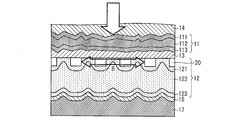
- FIG. 4 is a diagram showing the resonance effect of light by the first photonic crystal.
- FIG. 5 is a diagram showing the light confinement effect of the solar cell 1 in the present embodiment.
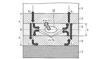
- FIG. 6 is a diagram illustrating a theoretical study model of the solar cell 1 for predicting the light absorption amount.
- the light taken into the solar cell 1 light having a short wavelength range is mainly absorbed by the first photoelectric conversion layer 11, and light not absorbed by the first photoelectric conversion layer 11 is second. Incident to the photoelectric conversion layer.
- the light incident on the second photoelectric conversion layer 12 is also referred to as incident light.
- the absorption of light in the second photoelectric conversion layer 12 will be described in particular.
- the second photoelectric conversion layer 12 of the theoretical study model in FIG. 6 includes a resonator 22 that confines incident light by resonating.
- the first photonic crystal including the nanorod 20 can be regarded as the resonator 22 shown in FIG. Further, an arrow B shown in FIG. 4 indicates that the incident light resonates only in the in-plane direction in the first photonic crystal.
- the entire first photonic crystal functions as one large resonator that resonates in the in-plane direction.
- the first photonic crystal can confine light not in a limited range of the first photonic crystal but in the entire first photonic crystal.
- the resonance effect of the resonator 22 formed in the first photonic crystal shown by the arrow B in FIG. 4 and the reflection effect by the metal electrode 17 on the back surface side (that is, incident light and metal on the second photoelectric conversion layer 12) Effect of light confinement due to the interaction with the reflected light from the electrode 17) and light confinement due to the vertical structure formed by the first photonic crystal and the second photonic crystal on the back side.
- the light incident on the second photoelectric conversion layer 12 is confined between the first photonic crystal and the metal electrode 17 as shown by an arrow A in FIG.
- the light absorption coefficient of the second photoelectric conversion layer 12 is ⁇
- the refractive index is n
- the Q value representing the magnitude of the resonance effect by the medium of the second photoelectric conversion layer 12 that can be derived from the light absorption coefficient ⁇ is Q ⁇ .
- the time change of the electric field amplitude a of the resonator 22 formed in the first photonic crystal under the modeled condition is shown as follows.
- the photonic crystal is regarded as an optical resonator, and a configuration in which the metal electrode 17 (reflectance 1.0) is disposed on the side opposite to the light incident side of the second photoelectric conversion layer is set as a modeled condition.
- the intermediate transparent conductive films 13 and 15 are assumed to have a refractive index and a light absorption rate of zero.
- the electric field amplitude of the light that passes through the first photoelectric conversion layer 11 and enters the second photoelectric conversion layer 12 is S + 1, and the light that passes from the second photoelectric conversion layer 12 to the metal electrode 17.
- the electric field amplitude is S-2
- the electric field amplitude of the light reflected by the metal electrode 17 and incident on the second photoelectric conversion layer 12 is S + 2
- the electric field of the light passing from the second photoelectric conversion layer 12 to the first photoelectric conversion layer 11 Let the amplitude be S-1.
- the square of the absolute value of each electric field amplitude represents light energy.
- the electric field amplitude of the resonator 22 formed in the first photonic crystal is a.
- the thickness from the resonator 22 to the metal electrode 17 is h
- the thickness of the second photoelectric conversion layer 12 is d
- the Q value according to the structure of the first photonic crystal is Qc.
- ⁇ indicates the phase state of light, and differs depending on the incident light and the state of the resonator 22.
- the electric field amplitude S-1, the electric field amplitude S-2, the electric field amplitude S + 1, and the electric field amplitude S + 2 are expressed by the following equations 4 to 6.
- ⁇ and ⁇ indicate the phase state of the light and differ depending on the incident light and the state of the resonator 22.
- the magnitude of light absorption in the second photoelectric conversion layer 12 including the resonator 22 is determined by the absorption of light in the second photoelectric conversion layer 12 due to resonance in the resonator 22 and the second photoelectric conversion layer 12. It can be represented by the sum of the absorption of light when passing through.
- the optimum conditions for light absorption can be obtained from the mode coupling theory considering light reflection and absorption.
- Qc can be said to be a Q value representing the strength of coupling of the first photonic crystal with the outside in the resonance mode, and can be said to be a finite time domain difference method (FDTD method: Finite Difference Time Domain method). )
- FDTD method Finite Difference Time Domain method
- the light absorption is determined by the light wavelength ⁇ c, the Q value (Qc) due to the structure of the resonator 22, the light absorption coefficient ⁇ , and the design of the first photonic crystal structure. Therefore, light absorption can be improved by optimally designing the first photonic crystal structure with respect to the light absorption coefficient ⁇ .
- the final light absorption is determined by the thickness h from the nanorod 20 to the metal electrode 17 and the height s of the nanorod 20 (see FIG. 5).
- FIG. 7 is a graph showing the intensity of light resonance with respect to the normalized frequency when an electromagnetic field analysis using the finite element method is performed on the first photonic crystal structure.
- a of FIG. 7 is a figure which shows the intensity
- (b) of FIG. 7 is from 0.25 to 0.30. It is a figure which shows the intensity
- the resonance of light with respect to the normalized frequency in the range near 0.30 is obtained.
- Strength is increasing.
- a mode in which the intensity of resonance of light increases with respect to the normalized frequency is also referred to as a resonance mode.
- the lattice constant p and the radius r of the nanorod 20 shown in FIG. 5 are obtained using the resonance mode at the lowest normalized frequency among the resonance modes obtained by electromagnetic field analysis using the finite element method. Therefore, it is preferable to design the structure of the first photonic crystal.
- FIG. 8 is a graph showing the relationship between the energy at each wavelength of sunlight and the sensitivity characteristic of the photoelectric conversion layer when the first photonic crystal is designed to improve the light absorption rate.
- the light with respect to the range indicated by the alternate long and short dash line, in particular, the light wavelength of 800 nm. Can be increased to approach the energy of sunlight.
- the second photoelectric conversion layer 12 absorbs light due to resonance. Increase effect can be obtained.
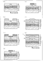
- FIG. 9 is a process diagram showing a manufacturing process of the solar cell 1.
- the medium of the first photoelectric conversion layer is a-Si
- the medium of the second photoelectric conversion layer is ⁇ c-Si
- the medium of the intermediate transparent conductive film 13 is SnO2
- the medium of the nanorod 20 is SiO2,
- the present invention is not limited to this.
- a transparent substrate 16 is formed, and SnO 2 is vapor-deposited thereon to form a transparent conductive film 14.
- a-Si is vapor-deposited on the entire surface of the transparent conductive film 14, and a p-type semiconductor layer 111 is formed by doping p-type impurities, and a-Si is vapor-deposited thereon to form an i-type semiconductor layer 112.
- the n-type semiconductor layer 113 is formed by further depositing a-Si thereon and doping an n-type impurity.
- the intermediate transparent conductive film 13 is formed by vapor-depositing SnO 2 on the n-type semiconductor layer 113. If the surface of the formed intermediate transparent conductive film 13 has an uneven shape, the surface is flattened. Further, SiO 2 which is a material for forming the nanorods 20 is deposited on the intermediate transparent conductive film 13 to form the SiO 2 layer 30.
- a pattern corresponding to the arrangement pattern of the nanorods 20 is drawn by electron beam exposure. If the photoresist 31 is a positive type photosensitive material, the arrangement pattern of the nanorods 20 is formed by removing the exposed portion by development.
- Al is deposited over the entire arrangement pattern to form an Al film 32.
- the photoresist 31 is removed to leave the Al film 32 only at the formation site of the nanorods 20.
- ICP-RIE Inductively coupled reactive ion etching
- CF4 carbon tetrafluoride
- the remaining Al film 83 is removed by wet etching using hydrochloric acid (HCl).
- ⁇ c-Si is deposited on the entire surface of the intermediate so as to cover the nanorods 20, and a p-type impurity is doped to form a p-type semiconductor layer 121.
- ⁇ c-Si is vapor-deposited on the p-type semiconductor layer 121 to form an i-type semiconductor layer 122.
- ⁇ c-Si is vapor-deposited thereon, and an n-type impurity is doped to form an n-type semiconductor layer 123. To do.
- SnO2 is vapor-deposited to form the transparent conductive film 15, and the metal electrode 17 is further laminated to complete the solar cell 1.
- the solar cell 1 absorbs light of a short wavelength in the first photoelectric conversion layer 11 and absorbs light of a long wavelength in the second photoelectric conversion layer 12, and thus absorbs light of a wide range of wavelengths. be able to.
- the first photonic crystal having a refractive index difference by the second photoelectric conversion layer 12 and the nanorod 20, the light taken into the solar cell 1 can be resonated (resonance effect). Further, the captured light diffracts or scatters when passing through the first photonic crystal due to the difference in refractive index of the first photonic crystal, so that the captured light can interfere with each other (interference effect).
- the solar cell 1 can confine the captured light by the resonance effect and the interference effect of the first photonic crystal.
- the second photoelectric conversion layer 12 is formed so as to cover the nanorods 20.
- the first photonic is not performed so as to prevent the second photoelectric conversion layer 12 from being damaged, such as embedding the nanorods 20 in the second photoelectric conversion layer 12. Crystals can be formed.
- the solar cell 1 can efficiently increase the light absorption rate in the second photoelectric conversion layer 12, particularly the light absorption rate at a long wavelength, and improve the photoelectric conversion rate.
- the amount of electromotive force in the solar cell 1 Can be increased.
- FIG. 10 is a top view schematically showing the structure of the first photonic crystal according to the present embodiment.
- the first photonic crystal according to the present embodiment is the first photonic crystal according to the first embodiment, except that cylindrical nanorods 201 are arranged in a triangular lattice shape. It has the same structure as the crystal.
- the first photonic crystal has a plurality of cylindrical nanorods 201 arranged at equal intervals with the adjacent nanorods 201 on the surface of the transparent conductive film 14. Are arranged in a triangular lattice pattern.
- the nanorod 201 has a hexagonal lattice (shown by thin lines in FIG. 10) that is composed of hexagonal vertices and centers composed of triangular lattices when viewed in plan. Then, since the lattice constant of the nanorod 201 is p (nm), two-dimensionally arranged hexagonal lattices are arranged at an arrangement interval of ⁇ 3p in the x direction and 2p in the y direction orthogonal to the x direction.
- the radius of the nanorod 201 is preferably in the range of 0.2p (diameter 0.4p) or more and 0.4p (diameter 0.8p) or less with respect to the lattice constant p.
- the first photonic crystal structure has a refractive index difference between the refractive index of the second photoelectric conversion layer 12 and the refractive index of the nanorod 201. become.
- the present invention is not limited to this, and for example, a quadrangular prism shape or a triangular prism shape. It may be formed.
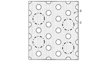
- FIG. 11 is a top view schematically showing the structure of the first photonic crystal when a defect is formed in the first photonic crystal.
- a region where the nanorods 201 are not provided, that is, a defect (also referred to as a cavity or a nanocavity) 21 is formed in a structure in which the nanorods 201 are periodically arranged.
- a defect level c is generated in the photonic band gap g of the first photonic crystal.
- Light in a wavelength band (allowable band) corresponding to the defect level c is allowed to exist in the defect 21, but is not allowed to exist in the first photonic crystal around the defect 21.
- the defect 21 becomes a minute resonator (resonator) that confines light in the wavelength band corresponding to the defect level c.
- the defect 21 is provided as a single lattice point defect that creates a region where one nanorod 201 is not provided, or a three-lattice dotted shape that creates a region where three nanorods 201 are not provided linearly. Defects etc. can be employed.
- the first photonic crystal constituted by the nanorod 201 and the defect 21 does not have a polarization characteristic or the like in a specific direction.
- the structure of the first photonic crystal is a symmetrical structure.
- the electromagnetic field obtained by the structure is desirably obtained in a concentric shape.
- FIG. 12 is a diagram showing a distribution of resonance intensity in the first photonic crystal when no defect is formed.
- FIG. 13 is a diagram showing the distribution of resonance intensity in the first photonic crystal when defects are formed.
- the defect 21 is formed in the first photonic crystal, as shown in FIG. 13, the weakly resonant portion D spreads over the entire first photonic crystal, and the strong resonant portion C is defective. Concentrate on 21. That is, when the defect 21 is formed in the first photonic crystal, resonance occurs around the defect 21.
- the portion C having strong resonance is distributed so as to concentrate on the defect 21. Therefore, by forming the defect 21 in the first photonic crystal, it is possible to obtain a resonance effect such that the portion C having strong resonance concentrates on the defect 21. In this way, light can be confined in the defect under the condition that a band gap can be obtained by the first photonic crystal formed in a triangular lattice structure.
- FIG. 14 is a graph showing the relationship between the energy at each wavelength of sunlight and the sensitivity characteristic of the photoelectric conversion layer when the first photonic crystal is formed by arranging the nanorods 20 in a triangular lattice shape.
- the intensity of light absorption with respect to the range indicated by the alternate long and short dash line, particularly the wavelength of light of 900 nm, can be close to the energy.
- the resonance method can be changed with respect to the case where the nanorods 20 constitute the first photonic crystal arranged in a square lattice shape, and can be resonated at different normalized frequencies. Further, by arranging the nanorods 20 forming the first photonic crystal in a triangular lattice shape, it is possible to design a structure of the first photonic crystal suitable for a wavelength band different from the case where the nanorods 20 are arranged in a square lattice shape. .
- the wavelength band of a band different from the case where the nanorods 20 are arranged in a square lattice form to form the first photonic crystal can be increased.
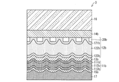
- FIG. 15 is a cross-sectional view schematically showing the overall configuration of the solar cell according to the present embodiment.
- the solar cell 2 according to this embodiment both the first photoelectric conversion layer 11 side and the second photoelectric conversion layer 12a side of the intermediate transparent conductive film 13a are formed flat.
- the nanorod 20a has the same configuration as that of the solar cell 1 of Embodiment 1 except that the nanorod 20a is formed along the surface shape of the intermediate transparent conductive film 13a.
- the intermediate transparent conductive film 13a is a transparent conductive film, and is disposed so as to be sandwiched between the first photoelectric conversion layer 11 and the second photoelectric conversion layer 12a. In addition, the intermediate transparent conductive film 13a is not processed so that both the first photoelectric conversion layer 11 side and the second photoelectric conversion layer 12a side are flat.
- the intermediate transparent conductive film 13a is made of a medium having a smaller refractive index than the medium of the first photoelectric conversion layer 11 and the second photoelectric conversion layer 12a.
- the medium include ITO (Indium-Tin-Oxide) and ZnO. , SnO2 and the like.
- the first photonic crystal is formed by periodically arranging a plurality of nanorods 20a on the surface of the transparent conductive film 14 having an uneven shape (surface shape). Further, the p-type semiconductor layer 121a of the second photoelectric conversion layer 12a is formed so as to cover the nanorod 20a and the transparent conductive film 14 from the side opposite to the light incident side, and further, the i-type semiconductor layer 122a and the n-type semiconductor layer 123a is formed.
- the nanorod 20a is a medium having a refractive index smaller than that of the medium of the second photoelectric conversion layer 12a.
- the nanorod 20a may be formed in a quadrangular prism shape or a cylindrical shape.
- air may be used, or SiO2 having a refractive index of 1.45 may be used.
- JAS transparent resin material
- HSQ Hydrophilicity Quadrature SQ
- SOG Spin-on Glass
- FOX Toray Dow Corning's registered trademark
- each nanorod 20a formed in a quadrangular prism shape or a cylindrical shape is arranged in a square lattice shape or a triangular lattice shape so that the arrangement intervals between adjacent nanorods 20a are equal to each other.
- a photonic crystal is formed.
- interval of adjacent nanorod 20a is also called the lattice constant p (nm).
- a region where the nanorods 20a are not provided, that is, defects 21 are formed in the structure in which the nanorods 20a are periodically arranged. Also good.
- the radius of the nanorod 20a is preferably in the range of 0.2p (diameter 0.4p) to 0.4p (diameter 0.8p) based on the lattice constant p.
- the first photonic crystal structure has a refractive index difference between the refractive index of the second photoelectric conversion layer 12a and the refractive index of the nanorod 20a. become.
- FIG. 16 is a cross-sectional view showing details of the shape of the intermediate transparent conductive film 13a.
- a transparent conductive film 14 having irregularities is formed on the surface on the first photoelectric conversion layer 11 side.
- the first photoelectric conversion layer 11 including the p-type semiconductor layer 111, the i-type semiconductor layer 112, and the n-type semiconductor layer 113 is formed by depositing a-Si along the uneven shape of the transparent conductive film 14. . Since the p-type semiconductor layer 111 of the first photoelectric conversion layer 11 is formed along the uneven shape of the transparent conductive film 14, the same uneven shape as the uneven shape of the transparent conductive film 14 is formed in the p-type semiconductor layer 111. Is done.
- the n-type semiconductor layer 113 of the first photoelectric conversion layer 11 has a concavo-convex shape similar to the concavo-convex shape of the transparent conductive film 14 although it is gentler than the p-type semiconductor layer 111.
- the intermediate transparent conductive film 13a is formed by vapor-depositing SnO2 along the uneven shape of the n-type semiconductor layer 113 of the first photoelectric conversion layer 11. At this time, the same uneven shape as the uneven shape of the n-type semiconductor layer 113 is formed on the surface of the intermediate transparent conductive film 13a. Thereby, although the uneven
- nanorods 20a are formed along the uneven shape on the surface of the intermediate transparent conductive film 13a. At this time, the uneven shape in the arrangement of the nanorods 20a is similar to the uneven shape of the intermediate transparent conductive film 13a.
- ⁇ c-Si is deposited, and a p-type semiconductor layer 121a is formed so as to cover the nanorods 20a from the side opposite to the light incident side. Further, ⁇ c-Si is deposited on the p-type semiconductor layer 121a to form an i-type semiconductor layer 122a and an n-type semiconductor layer 123a. At this time, the unevenness formed in the i-type semiconductor layer 122a of the p-type semiconductor layer 121a is gentler than that in the i-type semiconductor layer 122a, but is also formed in the n-type semiconductor layer 123a.
- the nanorods 20a forming the first photonic crystal are arranged along the uneven shape of the surface of the intermediate transparent conductive film 13a, the height of the light incident surface of the first photonic crystal is the light Is not uniform with respect to the incident direction. For this reason, in the first photonic crystal, a stronger light diffraction or scattering effect can be obtained, so that a strong interference effect can be obtained. Therefore, the light absorption rate can be further increased by the resonance effect and the strong interference effect in the first photonic crystal.
- the solar cell 1 As shown in FIG. 17, in the solar cell 3 according to this embodiment, the nanorods 20b and the second photoelectric conversion layer 12b are formed on the transparent substrate 16 side, and the first photoelectric conversion layer 11b is formed on the metal electrode 17 side. Except for this, the solar cell 1 has the same configuration as that of the first embodiment.
- FIG. 17 is a cross-sectional view schematically showing the overall configuration of the solar cell according to this embodiment.
- FIG. 18 is a figure which shows the detail of the transparent conductive film 14b of the solar cell 3, and the 2nd photoelectric converting layer 12b.
- a transparent conductive film 14 b having a flat surface shape is formed on the transparent substrate 16.
- nanorods 20b are periodically arranged on the planarized surface of the transparent conductive film 14b.
- a second photoelectric conversion layer 12b composed of a p-type semiconductor layer 121b, an i-type semiconductor layer 122b, and an n-type semiconductor layer 123b is formed so as to cover the nanorod 20b from the side opposite to the light incident side.
- an intermediate transparent conductive film 13b is formed next to the second photoelectric conversion layer 12b, and further, a first photoelectric conversion layer 11b including a p-type semiconductor layer 111b, an i-type semiconductor layer 112b, and an n-type semiconductor layer 113b. Is formed.
- a transparent conductive film 15b is formed, and a metal electrode 17 is formed.
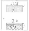
- FIG. 19 is a diagram schematically showing the incorporation of sunlight into the solar cell 3.
- FIG. 19 (a) shows the capture of sunlight when the first photonic crystal is not formed on the transparent conductive film 14b
- FIG. 19 (b) shows the first photonic crystal formed on the transparent conductive film 14b. Shows the uptake of sunlight.
- the refractive index of the transparent conductive film 14b is about 2 and the refractive index of the second photoelectric conversion layer 12b is about 3 to 4, as shown in FIG.
- a lot of incident sunlight is reflected at the boundary between the transparent conductive film 14b and the second photoelectric conversion layer 12b and is not taken into the second photoelectric conversion layer 12b. For this reason, the sunlight taken into the second photoelectric conversion layer 12b is reduced.
- the refractive index of the nanorod 20b is about 1.4 to 1.5
- the transparent conductive film 14b and the incident sunlight The refractive index difference from the photoelectric conversion layer through which the first passes can be reduced.
- the sunlight reflected at the boundary between the transparent conductive film 14b and the second photoelectric conversion layer 12b is reduced and diffracted or scattered. Sunlight taken into the second photoelectric conversion layer can be increased.
- the first photonic crystal formed on the transparent conductive film 14b performs a so-called structure function that is conventionally used to reduce light reflection at the interface of the solar cell. Therefore, by forming the first photonic crystal in the transparent conductive film 14b, the reflection of light can be reduced without forming a structure at the interface of the solar cell 3.
- the intermediate transparent conductive film 13 includes the first photoelectric conversion layer 11 side and the second photoelectric conversion layer 12 side, as in the solar cell 2 shown in FIG. Any of these surfaces may be formed flat, or any surface may not be formed flat.
- FIGS. 20 and 21 are top views schematically showing the structure of the first photonic crystal according to the present embodiment.
- the photonic crystal according to this embodiment is the same as that in Embodiment 1 except that cylindrical nanorods 203 to 206 are arranged so as to form two types of lattice structures.
- FIG. 20 shows a photonic crystal structure in which cylindrical nanorods 203 and 204 are two-dimensionally arranged on the same plane so that two types of lattice structures, a square lattice shape and a triangular lattice shape, are formed. It is a top view showing typically.
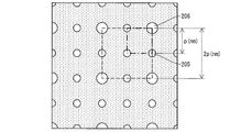
- FIG. 21 also shows a photo in which two types of cylindrical nanorods 205 and 206 having different radii are two-dimensionally arranged on the same plane so as to form two types of square lattice structures having different sizes. It is a top view which shows the structure of a nick crystal typically.
- the nanorods 203 arranged in a square lattice form a square lattice structure in which the length of one side is p (nm), that is, the lattice constant p.
- the nanorods 204 arranged in a triangular lattice form a triangular lattice structure in which the length of each side forming the hexagon is 2p (nm), that is, the lattice constant is 2p.
- the nanorod 203 and the nanorod 204 are formed in the same photonic crystal structure, and that the nanorod 203 and the nanorod 204 are not overlapped or in contact with each other.
- the radius of the nanorods 203 and 204 is preferably 0.2 times or more the lattice constant p.
- the nanorod according to the present embodiment includes two types of nanorods having different sizes, and the first lattice structure is formed by the plurality of small nanorods and one large nanorod, and the plurality of first lattices.
- the second lattice structure may be formed by large nanorods included in the structure.
- a nanorod 205 having a small radius and a nanorod 206 having a large radius have a square lattice structure (first lattice structure) in which the length of one side is p (nm), that is, the lattice constant p. Is forming.
- the nanorod 206 having a large radius forms a square lattice structure (second lattice structure) in which the length of one side is 2p (nm), that is, the lattice constant is 2p.
- the nanorod 205 and the nanorod 206 are formed in the same photonic crystal structure, and the radius of the nanorod 206 is preferably twice the radius of the nanorod 205.
- the first photonic crystal By forming the first photonic crystal in this way, there is a difference in refractive index between the refractive index of the second photoelectric conversion layer 12 and the refractive indexes of the nanorods 203 to 206 in the first photonic crystal structure. It will be.
- the refractive indexes of the nanorods 203 to 206 are preferably the same.
- the present invention is not limited to this and is formed in a quadrangular columnar shape. May be.
- the nanorods so as to have two types of lattice structures in the same photonic crystal structure, light of two types of wavelengths can be resonated in one photonic crystal. .
- the wavelength band of light that can be absorbed increases and the light absorption rate can be improved, so that the amount of electromotive force in the entire solar cell can be increased.
- the present invention is not limited to this and has three or more types of lattice structures.
- Nanorods may be placed.
- the nanorods may be arranged so as to form three types of lattice structures: a short square lattice structure with one side, a long square lattice structure with one side, and a triangular lattice structure.
- a solar cell panel in which a plurality of units are arranged one-dimensionally or two-dimensionally with the above-described solar cell as one unit is also one category of the present invention.
- a solar cell in which no defect is provided in the first photonic crystal is easier to manufacture than a solar cell in which a defect is provided in the first photonic crystal. Therefore, the solar cell panel in which the solar cells not provided with defects in the first photonic crystal are arranged has an advantage of being suitable for mass production.
- an apparatus provided with any of the above-described solar cells as a power source is also one category of the present invention.
- Such devices include portable or stationary electronic devices, home appliances, advertising towers, and the like that operate using the solar cell as a power source.
- an apparatus provided with a solar cell panel as a power source is also one category of the present invention.
- Such devices include vehicles or advertising towers in addition to portable or stationary electronic devices or home appliances that operate using the solar cell panel as a power source.
- the solar cell according to one embodiment of the present invention mainly includes a first photoelectric conversion layer that mainly absorbs light having a short wavelength and performs photoelectric conversion, and a first photoelectric layer that mainly absorbs light having a long wavelength and performs photoelectric conversion.
- the first photonic crystal is formed with the above medium.
- the solar cell absorbs light on the short wavelength side in the first photoelectric conversion layer, and absorbs light on the long wavelength in the second photoelectric conversion layer. For this reason, light of a wide range of wavelengths can be absorbed.
- the first photonic crystal having a refractive index difference is constituted by the second photoelectric conversion layer and the plurality of columnar media, so that the light taken into the solar cell can be captured. It can resonate (resonance effect). Further, the sun leaks from the light leaking from the first photonic crystal and the light that passes through the second conversion layer and is incident again from the surface opposite to the light incident side of the second conversion layer. The light taken into the battery can interfere with each other (interference effect).
- the solar cell can confine the captured light by the resonance effect and the interference effect of the first photonic crystal.
- the path of light passing through the second photoelectric conversion layer can be increased. Therefore (diffraction scattering effect), the light absorption rate can be increased.
- the solar cell is formed so that the second photoelectric conversion layer covers the plurality of columnar media.
- the second photoelectric conversion layer is embedded in the plurality of columnar media so as not to perform processing that damages the second photoelectric conversion layer.
- a first photonic crystal can be formed.
- the solar cell can efficiently increase the light absorption rate in the second photoelectric conversion layer, particularly the light absorption rate at a long wavelength, and improve the photoelectric conversion rate.
- the amount of electromotive force in the solar cell Can be increased.
- the first photoelectric conversion layer is disposed on the side opposite to the light incident side of the second photoelectric conversion layer with the first transparent conductive film interposed therebetween, and the second photoelectric conversion is performed.
- a second transparent conductive film is disposed on the light incident side of the layer, and the second photoelectric conversion layer covers the second transparent conductive film and the plurality of columnar media from the side opposite to the light incident side. It is preferable to be formed.
- the photoelectric conversion layer through which the incident light first passes is, of the two photoelectric conversion layers, the second transparent conductive film and the plurality of columnar media opposite to the light incident side. It is the 2nd photoelectric converting layer formed so that it might cover.
- the first photonic crystal is formed between the second transparent conductive film and the second photoelectric conversion layer, refraction of the second transparent conductive film and the second photoelectric conversion layer is performed. The rate difference can be reduced.
- the amount of reflected light is reduced and the light is diffracted or scattered to be taken into the second photoelectric conversion layer. be able to.
- the reflection of light can be reduced without forming a so-called structure that is conventionally used to reduce the reflection of light at the interface of the solar cell.
- the plurality of columnar media have a refractive index smaller than that of the medium of the second photoelectric conversion layer and are arranged in a square lattice pattern.
- the second photoelectric conversion layer includes the first column in which the plurality of columnar media are arranged in a square lattice shape, that is, at equal intervals in the row direction and the column direction, together with the plurality of columnar media.
- the photonic crystal is applied to light incident from a square lattice-shaped row direction and a column direction in which the plurality of columnar media are arranged on the surface constituting the first photonic crystal. It is possible to obtain the above-described effects (light confinement effect due to resonance effect and interference effect, and diffraction scattering effect).
- the component in the row direction can be regarded as the light incident from the row direction, and the component in the column direction is the light incident from the column direction. Can be considered. For this reason, the effect of the photonic crystal can be obtained for light incident from a direction having an angle with respect to the row direction as well as light incident from the row direction and the column direction.
- the plurality of columnar media in the solar cell according to one embodiment of the present invention is preferably formed in a columnar shape, a quadrangular columnar shape, or a triangular columnar shape.
- the light incident from any direction with respect to the surface constituting the first photonic crystal can resonate substantially evenly. Can do.
- the isotropic property on the light incident side is smaller than in the case where the plurality of columnar media are formed in a columnar shape. Therefore, although the resonance effect of light is reduced, the manufacturing cost can be suppressed because the manufacturing is easy.
- the shape of the columnar medium is a columnar shape, a quadrangular columnar shape or a triangular columnar shape may be determined in consideration of the trade-off relationship between the resonance effect and the manufacturing cost.
- the solar cell according to one embodiment of the present invention further includes a first transparent conductive film between the first photoelectric conversion layer and the second photoelectric conversion layer, and the plurality of columnar media includes the first transparent conductive film.
- the second photoelectric conversion layer is formed so as to cover the first transparent conductive film and the plurality of columnar media from the side opposite to the light incident side. It is preferable.
- the first photonic crystal can be formed along the surface shape of the first transparent conductive film. That is, when the first photonic crystal is formed, if the surface of the first transparent conductive film is uneven, the first photonic crystal can be formed along the uneven shape. .
- the plurality of columnar media have a refractive index smaller than that of the medium of the second photoelectric conversion layer and are arranged in a triangular lattice shape.
- the first photonic crystal in which the columnar medium is arranged in a triangular lattice shape is configured.
- the resonance method can be changed as compared with the case where the first photonic crystal in which the plurality of columnar media are arranged in a square lattice is used, and resonance is performed at different normalized frequencies. be able to.
- a first photonic crystal having a structure suitable for a wavelength band of light different from that of the first photonic crystal in which the plurality of columnar media are arranged in a square lattice pattern.
- the light absorptance of the wavelength band different from the case where the first photonic crystal in which the plurality of columnar media are arranged in a square lattice shape can be increased.
- the plurality of columnar media in the solar cell according to one embodiment of the present invention is further formed in a columnar shape or a square columnar shape.
- the light incident from any direction with respect to the surface constituting the first photonic crystal can resonate substantially evenly. Can do.
- the isotropic property in the light incident side is smaller than when the plurality of columnar media are formed in a columnar shape.
- the resonance effect of light is reduced, the manufacturing cost can be suppressed because the manufacturing is easy.
- the shape of the columnar medium is a columnar shape or a quadrangular column shape may be determined in consideration of the trade-off relationship between the resonance effect and the manufacturing cost.
- the first photonic crystal has a photonic band gap, and the triangular lattice-like portion is formed on a part of the triangular lattice so as to generate a defect level in the photonic band gap. It is preferable that the first photonic crystal has a defect in which a plurality of columnar media are not arranged.
- the second photoelectric conversion layer is formed so as to cover the first photonic crystal in which the defect is formed so as to generate a defect level in the photonic band gap.
- light having a specific wavelength corresponding to the defect level is confined in and near the defect of the first photonic crystal and causes resonance.
- the resonance effect can be concentrated on the defects of the first photonic crystal, the light absorption rate can be increased.
- the solar cell according to one embodiment of the present invention further includes a first transparent conductive film between the first photoelectric conversion layer and the second photoelectric conversion layer, and the plurality of columnar media includes the first transparent conductive film.
- the second photoelectric conversion layer is formed so as to cover the first transparent conductive film and the plurality of columnar media from the side opposite to the light incident side. It is preferable.
- the first photonic crystal can be formed along the surface shape of the first transparent conductive film. That is, when the first photonic crystal is formed, if the surface of the first transparent conductive film is uneven, the first photonic crystal can be formed along the uneven shape. .
- the solar cell which concerns on 1 aspect of this invention is further equipped with the 3rd transparent conductive film formed along the uneven
- the said 2nd photoelectric conversion It is preferable that the second photonic crystal is constituted by the concavo-convex shape of the surface of the layer and the third transparent conductive film.
- the second photoelectric conversion layer forms the first photonic crystal on the light incident side, and further forms the second photonic crystal on the side opposite to the light incident side. Will do. Accordingly, light can be further confined in the second photoelectric conversion layer by the first photonic crystal and the second photonic crystal.
- the plurality of columnar media in the solar cell according to one embodiment of the present invention are arranged to form a plurality of types of lattice structures.
- the plurality of types of lattice structures are configured include, for example, a case where the plurality of columnar media are arranged so as to have two types of lattice structures, a square lattice structure and a triangular lattice structure. be able to. Further, the plurality of columnar media may be arranged so as to have three or more types of lattice structures such as a square lattice structure with a short side, a square lattice structure with a long side, and a triangular lattice structure.
- the plurality of columnar media includes two types of columnar media, and each of the plurality of columnar media includes a plurality of small columnar media and one large columnar medium.
- the first lattice structure is formed, and the second lattice structure is formed by a large columnar medium included in the plurality of first lattice structures.
- a solar cell panel according to an aspect of the present invention is characterized in that the above-described solar cell is used as one unit and includes a plurality of units arranged one-dimensionally or two-dimensionally.
- a solar cell in which no defect is provided in the first photonic crystal is easier to manufacture than a solar cell in which a defect is provided in the first photonic crystal. Therefore, the solar cell panel in which the solar cells not provided with defects in the first photonic crystal are arranged has an advantage of being suitable for mass production.
- An apparatus provided with any of the above solar cells as a power source is also one category of the present invention.
- Such devices include portable or stationary electronic devices, home appliances, advertising towers, and the like that operate using the solar cell as a power source.
- the apparatus provided with the said solar cell panel as a power supply is also one category of this invention.
- Such devices include vehicles or advertising towers in addition to portable or stationary electronic devices or home appliances that operate using the solar cell panel as a power source.
- a combination of a configuration described in a certain claim and a configuration described in another claim is limited to a combination of the configuration described in the claim cited in the claim.
- combinations with configurations described in the claims not cited in the focused claims are possible.
- the present invention can be used for solar cells in general.
Landscapes
- Physics & Mathematics (AREA)
- Chemical & Material Sciences (AREA)
- Crystallography & Structural Chemistry (AREA)
- General Physics & Mathematics (AREA)
- Optics & Photonics (AREA)
- Photovoltaic Devices (AREA)
Abstract
本発明の一態様に係る太陽電池(1)は、主に短波長の光を吸収して光電変換する第1光電変換層(11)と、主に長波長の光を吸収して光電変換する第2光電変換層(12)と、複数のナノロッド(20)と、を備え、第2光電変換層(12)は、複数のナノロッド(20)を、光の入射側と反対側から覆うように形成され、複数のナノロッド(20)と共に第1のフォトニック結晶を構成していることを特徴としている。
Description
本発明は、タンデム方式の太陽電池、複数の上記太陽電池を配列した太陽電池パネルおよび上記太陽電池を電源として搭載した装置に関するものである。
近年、太陽電池は、一般的に、光を電気に変換する光電変換層の媒質における光吸収が、波長によって異なり、特に、長波長側の光の吸収率が低いことが課題となっている。この課題を改善するために、アモルファスシリコン(a-Si)を媒質に用いた光電変換層に、微結晶シリコン(μc-Si)を媒質に用いた光電変換層を重ねて2層製膜するタンデム方式の太陽電池が実用化されてきている。なお、タンデム方式の太陽電池は、コストの面からも、薄膜太陽電池として、有望視されている。
ここで、従来用いられているタンデム方式の太陽電池における、各波長における太陽光のエネルギーと光電変換層の感度特性との関係を図22に示す。図22は、太陽光の各波長におけるエネルギーと光電変換層の感度特性との関係を示すグラフである。
図22に示す破線は、太陽光の各波長におけるエネルギー(以降、単に光エネルギーとも呼称する)の強度を示している。また、細線は、光電変換層の媒質にアモルファスシリコンを用いたa-Si光電変換層の感度特性、すなわち、光吸収の強度を示し、太線は、光電変換層の媒質に微結晶シリコンを用いたμc-Si光電変換層の感度特性、すなわち、光吸収の強度を示している。
図22に示すように、a-Si光電変換層は、波長が700nm程度以下の範囲に光吸収があり、特に波長が500nm程度付近において光吸収の強度が大きくなる。また、μc-Si光電変換層は、波長が450nm程度から950nm程度までの範囲に光吸収があり、特に、波長が600nm程度から700nm程度までの範囲において光吸収の強度が大きくなる。図22に示すように、a-Si光電変換層及びμc-Si光電変換層を有する従来のタンデム方式の太陽電池は、波長が750nm程度以下の範囲において、光の吸収効率を2層が補完し合うので、効率よく光を吸収することができている。
また、特許文献1には、太陽光をより効率よく受信して太陽電池に供給する技術が開示されている。図23に、特許文献1に係る太陽電池の概要を表す断面図を示す。
図23に示すように、特許文献1に係る太陽電池は、太陽電池表面に設けられた、誘電体アンテナと呼ばれる透明な材料(有機又は無機を問わず、例えば、ポリエチレン及びSiO2など)をロッド状にし、光との相互作用を起こすことによって、外部からの光の取り込み量を増やしている。これにより、本来なら表面反射を起こして取り込むことのできない光を取り込み、起電力を増加させている。
しかしながら、特許文献1に開示された太陽電池には、以下のような問題点が存在する。特許文献1に記載の太陽電池は、取り込む光の量を増やしているものの、光吸収の小さい長波長側において光の吸収率を向上させるものではないため、依然として長波長側の光の吸収率が低いという問題がある。
また、特許文献1に記載の太陽電池は、誘電体アンテナを用いることにより、さまざまな角度からの入射光を通常よりも多く取り込むことができ、これによって、太陽電池全体での光の吸収量を向上させている。しかし、特許文献1に記載の太陽電池では、取り込んだ光を太陽電池内に閉じ込めておくことはできないため、効率よく光を取り込むことはできても、取り込んだ光を効率よく吸収することはできない。したがって、取り込まれた光のうち、吸収されない光が太陽電池内に多く存在してしまい、光の吸収率を効率よく向上させることができないという問題がある。
また、タンデム方式の太陽電池においても、図22の一点鎖線で囲む領域に示されるように、波長が750nm程度から950nm程度までの範囲、すなわち、長波長における光の吸収率が低いという問題がある。
本発明は、上記の問題点に鑑みてなされたものであり、その目的は、特に長波長における光の吸収率を高めた太陽電池を提供することにある。
本発明の一態様に係る太陽電池は、上記の課題を解決するために、主に短波長の光を吸収して光電変換する第1光電変換層と、主に長波長の光を吸収して光電変換する第2光電変換層と、複数の柱状の媒質と、を備え、上記第2光電変換層は、上記複数の柱状の媒質を、光の入射側と反対側から覆うように形成され、上記複数の柱状の媒質と共に第1のフォトニック結晶を構成していることを特徴としている。
上記の構成によれば、上記太陽電池は、上記第1光電変換層において短波長側の光を吸収し、上記第2光電変換層において長波長の光を吸収する。このため、広範囲の波長の光を吸収することができる。
また、上記太陽電池は、上記第2光電変換層及び上記複数の柱状の媒質によって、屈折率差が存在する上記第1のフォトニック結晶を構成することにより、上記太陽電池内に取り込んだ光を共振させることができる(共振効果)。また、上記第1のフォトニック結晶から漏れた光と、上記第2変換層を通過した後上記第2変換層の光の入射側と反対側の面から再び入射される光とにより、上記太陽電池内に取り込んだ光を互いに干渉させることができる(干渉効果)。
上記太陽電池は、この上記第1のフォトニック結晶の共振効果と、干渉効果とにより、取り込んだ光を閉じ込めることを可能としている。加えて、共振効果や干渉効果を得られない光が上記第1のフォトニック結晶を通過する際に、回折または散乱するため、第2光電変換層を通過する光の経路を増加させることができるので(回折散乱効果)、光の吸収率を増加させることができる。
さらに、上記太陽電池は、上記第2光電変換層が、上記複数の柱状の媒質を覆うように形成されている。これによって、上記太陽電池を製造する際に、上記第2光電変換層に上記複数の柱状の媒質を埋め込むなど、上記第2光電変換層に対してダメージを与えるような加工を行わないように上記第1のフォトニック結晶を形成することができる。
したがって、上記太陽電池は、上記第2光電変換層における光の吸収率、特に長波長における光の吸収率を効率的に高め、光電変換率を向上させることができ、上記太陽電池における起電力量を増大させることができる。
本発明の一態様に係る太陽電池パネルは、上記の課題を解決するために、太陽電池を1ユニットとして、一次元的または二次元的に配列された複数の上記ユニットを備えたことを特徴としている。
これにより、光の吸収率が高い太陽電池が配列されているので、光電変換率の高い太陽電池パネルを得ることができる。
特に、第1のフォトニック結晶中に欠陥を設けていない太陽電池は、第1のフォトニック結晶中に欠陥を設けた太陽電池より製造しやすい。したがって、上述した第1のフォトニック結晶中に欠陥を設けていない太陽電池が配列された太陽電池パネルは、量産に適しているというメリットを持っている。
上記太陽電池のいずれかを電源として備えた装置もまた、本発明の1つのカテゴリーである。そのような装置には、上記太陽電池を電源として動作する携帯型または据え置き型の電子機器、家電製品または広告塔などが含まれる。
また、上記太陽電池パネルを電源として備えた装置もまた、本発明の1つのカテゴリーである。そのような装置には、上記太陽電池パネルを電源として動作する携帯型または据え置き型の電子機器または家電製品のほかに、車両または広告塔なども含まれる。
本発明の一態様に係る太陽電池は、以上のように、主に短波長の光を吸収して光電変換する第1光電変換層と、主に長波長の光を吸収して光電変換する第2光電変換層と、第1のフォトニック結晶と、を備え、上記第2光電変換層は、上記第1のフォトニック結晶を覆うように形成されていることを特徴としている。
したがって、上記太陽電池は、上記第2光電変換層における光の吸収率、特に長波長における光の吸収率を効率的に高め、光電変換率を向上させることができる。
<実施形態1>
本発明に係る太陽電池の一実施形態について、図1から図9を参照して以下に説明する。但し、本実施形態に記載されている構成部品の寸法、材質、形状、その相対配置などは、特に特定的な記載がない限り、この発明の範囲をそれのみに限定する趣旨ではなく、単なる説明例に過ぎない。
本発明に係る太陽電池の一実施形態について、図1から図9を参照して以下に説明する。但し、本実施形態に記載されている構成部品の寸法、材質、形状、その相対配置などは、特に特定的な記載がない限り、この発明の範囲をそれのみに限定する趣旨ではなく、単なる説明例に過ぎない。
(太陽電池の構成)
まず、本実施形態に係る太陽電池の構成例について、図1を参照して説明する。図1は、本実施形態の太陽電池1の全体構成を概略的に示す断面図である。
まず、本実施形態に係る太陽電池の構成例について、図1を参照して説明する。図1は、本実施形態の太陽電池1の全体構成を概略的に示す断面図である。
太陽電池1は、入射された光を、光電変換することで電流に変換して用いることができる。図1に示すように、太陽電池1は、第1光電変換層11、第2光電変換層12、中間透明導電膜(第1透明導電膜)13、透明導電膜(第2透明導電膜)14、透明導電膜15(第3透明導電膜)、透明基板16、及び、金属電極17を備えている。
また、第2光電変換層12には、図1に示すように、ナノロッド(柱状の媒質)20が周期的に配置された第1のフォトニック結晶構造が形成されている。より具体的には、第2光電変換層12が、複数のナノロッド20を光の入射側と反対側から覆うように形成されることで、複数のナノロッド20と共に第1のフォトニック結晶を構成している。
第1光電変換層11は、主に短波長の光を吸収して光電変換する半導体層である。また、第1光電変換層11は、極性の異なる半導体層が隣接した構造を有しており、その構造は特に限定されないが、例えば、i型半導体層(いわゆる、真性半導体層)112をp型半導体層111とn型半導体層113とで挟んだpin縦型構造を採用してもよい。また、第1光電変換層11の媒質としては、屈折率が3.0~4.0程度のアモルファスシリコン(a-Si)を挙げることができるが、これに限定されるものではなく、例えば、Si、Ge、GaNINGaP、(In)GeAs、GaAsなどであってもよい。
第2光電変換層12は、主に長波長の光を吸収して光電変換する半導体層である。第2光電変換層12もまた、第1光電変換層11と同様に、極性の異なる半導体層が隣接した構造を有しており、例えば、i型半導体層122をp型半導体層121とn型半導体層123とで挟んだpin縦型構造を採用してもよい。また、第2光電変換層12の媒質としては、例えば、屈折率が3.0~4.0の程度の微結晶シリコン(μc-Si)を挙げることができるが、これに限定されるものではない。例えば、ポリシリコン(p-Si:高純度多結晶シリコン)であってもよい。さらに、第2光電変換層12のp型半導体層121は、ナノロッド20が周期的に配置された第1のフォトニック結晶を覆うように形成されている。なお、ナノロッド20、及び、第1のフォトニック結晶については後述する。
中間透明導電膜13は、透明な導電膜であり、第1光電変換層11及び第2光電変換層12に挟まれるように配されている。また、透明導電膜(TCO;Transparent Conducing Oxide)14、15は、透明な導電膜であり、第1光電変換層11及び第2光電変換層12を挟んで配されている。
また、図1に示すように、中間透明導電膜13における、第1光電変換層11側、又は、第2光電変換層12側の何れか1方の面が平坦になるよう、平坦化する。なお、中間透明導電膜13の厚さを、例えば、300nmから400nm程度に厚くすることによって、中間透明導電膜13の第1光電変換層11側、又は、第2光電変換層12側の何れかの面を平坦にすることができる。すなわち、中間透明導電膜13の厚さを厚くすることによって、平坦化する処理を省くことができる。
なお、中間透明導電膜13、透明導電膜14及び15は、第1光電変換層11及び第2光電変換層12の媒質よりも屈折率が小さい媒質からなり、媒質としては、例えば、ITO(Indium-Tin-Oxide)、ZnO、SnO2などを挙げることができる。また、透明導電膜14は、透明導電膜15との間に第1光電変換層11及び第2光電変換層12を挟んで透明基板16側に配され、透明導電膜15は、透明導電膜14との間に第1光電変換層11及び第2光電変換層12を挟んで金属電極17側に配されている。
透明基板16の材料としては、例えば、屈折率が1.52程度のガラスを選択できる。また、金属電極17の材料としては、光反射率が高く、電気伝導度が大きな材料、例えば、AgまたはAlなどを選択できる。
透明基板16を介して第1光電変換層11及び第2光電変換層12に入射した光は、主にi型半導体層112、122において、電子と正孔とを発生させるとともに、電子を価電子帯から導電帯へと励起することによって、吸収される。
なお、金属電極17を、反射板としても機能させることができ、第1光電変換層11及び第2光電変換層12で光電変換されず、透過してきた光を、再び第1光電変換層11及び第2光電変換層12へと反射させることもできる。金属電極17を、太陽電池1の裏面の全面を覆って配することで、第1光電変換層11及び第2光電変換層12を透過した光を確実に反射することができるので、より、光の吸収効率が高い太陽電池1を構成することができる。
(第1のフォトニック結晶の構造)
次に、ナノロッド20、及び、第1のフォトニック結晶について、図2及び図3を参照して説明する。図2は、第1のフォトニック結晶を構成するナノロッド20が円柱である場合の、第1のフォトニック結晶構造の上面図である。また、図3は、第1のフォトニック結晶構造の上面図である。図3の(a)は、第1のフォトニック結晶を構成するナノロッド20が四角柱である場合の、第1のフォトニック結晶構造を示し、図3の(b)は、第1のフォトニック結晶を構成するナノロッド20が三角柱である場合の、第1のフォトニック結晶構造を示している。
次に、ナノロッド20、及び、第1のフォトニック結晶について、図2及び図3を参照して説明する。図2は、第1のフォトニック結晶を構成するナノロッド20が円柱である場合の、第1のフォトニック結晶構造の上面図である。また、図3は、第1のフォトニック結晶構造の上面図である。図3の(a)は、第1のフォトニック結晶を構成するナノロッド20が四角柱である場合の、第1のフォトニック結晶構造を示し、図3の(b)は、第1のフォトニック結晶を構成するナノロッド20が三角柱である場合の、第1のフォトニック結晶構造を示している。
図2及び図3に示すように、本実施形態において、第1のフォトニック結晶は、複数のナノロッド20が、透明導電膜14の表面に周期的に配置されて形成されている(いわゆる、二次元第1のフォトニック結晶)。また、ナノロッド20及び透明導電膜14を、光の入射側と反対側から覆うように第2光電変換層12のp型半導体層121が形成されている。
ナノロッド20は、第2光電変換層12の媒質より屈折率が小さい媒質で、例えば、図2に示すように円柱状に形成され、図3の(a)に示すように四角柱状に形成され、又は、図3の(b)に示すように三角柱状に形成されている。ナノロッド20の媒質としては、例えば、空気であってもよいし、屈折率が1.45のSiO2であってもよい。このほかに、ナノロッド20の材料として、屈折率1.6程度のJAS(有機絶縁性の透明樹脂材料)、SOG(Spin-on Glass)材料として用いられるHSQ(Hydrogen Silsequioxane:水素シルセスオキサン)として、例えばFOX(東レ・ダウコーニング社の登録商標)などを用いることもできる。
なお、図2に示すように、円柱状に形成された各ナノロッド201は、隣接するナノロッド201との配置間隔(ピッチ)が等間隔になるよう、正方格子状に配置されている。なお、隣接するナノロッド201同士の配置間隔の値を、格子定数p(nm)とも呼称する。
図3の(a)に示すように、四角柱状に形成された各ナノロッド202もまた、隣接するナノロッド202同士の配置間隔、すなわち、格子定数p(nm)が等間隔になるよう、正方格子状に配置されている。
さらに、図3の(b)に示すように、三角柱状に形成された各ナノロッド207もまた、隣接するナノロッド207同士の配置間隔、すなわち、格子定数p(nm)が等間隔になるよう、正方格子状に配置されている。
さらに、ナノロッド20の半径は、格子定数pを基準として、0.2p(直径0.4p)以上、0.4p(直径0.8p)以下の範囲を取ることが好ましい。
このように第1のフォトニック結晶を形成することにより、第1のフォトニック結晶構造には、第2光電変換層12の屈折率と、ナノロッド20の屈折率との屈折率差が存在することになる。
また、第2光電変換層12のp型半導体層121を、ナノロッド20を光の入射側と反対側から覆うように形成することによって、図1に示すように、p型半導体層121のi型半導体層122側は、凹凸形状となる。この凹凸形状は、p型半導体層121のi型半導体層122側と比較すれば緩やかではあるが、n型半導体層123にも形成される。このn型半導体層123の凹凸形状における凸形状部分と、n型半導体層123の凹形状部分の透明導電膜15とによって、第2のフォトニック結晶構造が形成されることになる。
なお、本実施形態においては、ナノロッド20が円柱状に形成されている場合を例に挙げて説明する。
(フォトニックバンド構造)
上記のような構成を備えた第1のフォトニック結晶には、フォトニックバンド構造が生成される。フォトニックバンド構造は、第1のフォトニック結晶に対する光の入射方向と、規格化周波数との関係によって表される。
上記のような構成を備えた第1のフォトニック結晶には、フォトニックバンド構造が生成される。フォトニックバンド構造は、第1のフォトニック結晶に対する光の入射方向と、規格化周波数との関係によって表される。
より具体的には、ナノロッド20の媒質による低誘電バンドと、第2光電変換層12の媒質による高誘電バンドとが生成される。なお、フォトニックバンド構造には、第1のフォトニック結晶内で存在できない光の波長帯域として、低誘電バンドと高誘電バンドとに挟まれたフォトニックバンドギャップgが含まれている。
規格化周波数は、第1のフォトニック結晶の格子定数pと光の周波数とが相関関係にあるために用いられるパラメータであり、p/λとして表される。
(光吸収の最適条件)
次に、本実施形態に係る太陽電池1における光吸収の最適条件について、図4から図6を参照して説明する。図4は、第1のフォトニック結晶による光の共振効果を示す図である。図5は、本実施形態における太陽電池1の光の閉じ込め効果を示す図である。図6は、光吸収量を予測する、太陽電池1の理論検討モデルを示す図である。
次に、本実施形態に係る太陽電池1における光吸収の最適条件について、図4から図6を参照して説明する。図4は、第1のフォトニック結晶による光の共振効果を示す図である。図5は、本実施形態における太陽電池1の光の閉じ込め効果を示す図である。図6は、光吸収量を予測する、太陽電池1の理論検討モデルを示す図である。
まず、太陽電池1に取り込まれた光のうち、波長が短波長の範囲の光は、主に第1光電変換層11において吸収され、第1光電変換層11において吸収されなかった光が第2光電変換層に入射される。以降では、第2光電変換層12に入射される光を入射光とも呼称する。本実施形態においては、特に、第2光電変換層12における光の吸収について説明する。なお、図6における理論検討モデルの第2光電変換層12は、入射光を共振させることによって閉じ込める共振器22を備えている。
ここで、ナノロッド20を含んで構成される第1のフォトニック結晶を、図6に示す共振器22とみなすことができる。また、図4に示す矢印Bは、第1のフォトニック結晶において、入射光が面内方向にのみ共振することを示している。
つまり、第1のフォトニック結晶全体が、面内方向にて共振する1つの大きな共振器として機能する。これによって、第1フォトニック結晶は、光を、第1のフォトニック結晶の限定した範囲に閉じ込めるのではなく、第1のフォトニック結晶全体に閉じ込めることができる。
図4の矢印Bに示す、第1のフォトニック結晶において形成される共振器22の共振効果と、裏面側の金属電極17による反射効果(すなわち、第2光電変換層12への入射光と金属電極17による反射光との干渉効果)との相互作用による光閉じ込めの効果と、第1のフォトニック結晶と、裏面側の第2のフォトニック結晶とで作られる縦方向の構造による光閉じ込めの効果とによって、図5の矢印Aに示すように、第2光電変換層12に入射された光は、第1のフォトニック結晶と金属電極17との間で閉じ込められることになる。
第2光電変換層12の光吸収係数をα、屈折率をnとし、光吸収係数αから導くことのできる、第2光電変換層12の媒質による共鳴効果の大きさを表すQ値をQαとすると、光の波長λcに対して、次式のようになる。なお、Q値は、電気工学の共振のQ値と同様、電磁波としての光の共鳴効果の大きさを表す。
Qα=2πn/(λcα) ・・・式1
さらに、式1を、光速c0、及び、共振角周波数ω0(ω0=2πc0/λc)を用いて表すと、次式のように表される。ここでは、金属電極17における光の反射は、完全反射(すなわち、反射率1.0)であるとする。以降では、金属電極17において反射する光を、反射光とも呼称する。
さらに、式1を、光速c0、及び、共振角周波数ω0(ω0=2πc0/λc)を用いて表すと、次式のように表される。ここでは、金属電極17における光の反射は、完全反射(すなわち、反射率1.0)であるとする。以降では、金属電極17において反射する光を、反射光とも呼称する。
ω0/Qα=αc0/n ・・・式2
ここで、モデル化した条件で第1のフォトニック結晶において形成される共振器22の電界振幅aの時間変化を定式化した、モード結合理論による理論式を、次式に示す。なお、本実施形態においては、光の入射側の面及び入射側と反対側の面を中間透明導電膜13及び透明導電膜15でそれぞれ覆われた第2光電変換層12が、ナノロッド20と共に形成するフォトニック結晶を光共振器とみなし、第2光電変換層の光の入射側と反対側に金属電極17(反射率1.0)が配置されている構成を、モデル化した条件としている。また、中間透明導電膜13、15は屈折率及び光吸収率が0であるとする。
ここで、モデル化した条件で第1のフォトニック結晶において形成される共振器22の電界振幅aの時間変化を定式化した、モード結合理論による理論式を、次式に示す。なお、本実施形態においては、光の入射側の面及び入射側と反対側の面を中間透明導電膜13及び透明導電膜15でそれぞれ覆われた第2光電変換層12が、ナノロッド20と共に形成するフォトニック結晶を光共振器とみなし、第2光電変換層の光の入射側と反対側に金属電極17(反射率1.0)が配置されている構成を、モデル化した条件としている。また、中間透明導電膜13、15は屈折率及び光吸収率が0であるとする。
なお、図6に示すように、第1光電変換層11を抜けて第2光電変換層12に入射する光の電界振幅をS+1、第2光電変換層12から金属電極17に抜けていく光の電界振幅をS-2、金属電極17で反射して第2光電変換層12に入射する光の電界振幅をS+2、第2光電変換層12から第1光電変換層11に抜けていく光の電界振幅をS-1とする。また、それぞれの電界振幅の絶対値の2乗は、光のエネルギーを表す。
また、第1のフォトニック結晶において形成される共振器22の電界振幅をaとする。また、図5に示すように、共振器22から金属電極17までの厚みをh、第2光電変換層12の厚みをd、第1のフォトニック結晶の構造によるQ値をQcとする。

ここで、φは、光の位相状態を示し、入射光や、共振器22の状態により異なる。なお、式3において、

は、電界振幅aの時間変化(時間発展)を示している。
また、式3において、

は、共振器22中の電界変化を示している。
さらに、式3において、

は、入射光及び反射光と共振器22との結合を示している。
また、電界振幅S-1、電界振幅S-2、電界振幅S+1及び電界振幅をS+2は、下記に示す式4から式6によって表される。



ここで、β及びΔは、光の位相状態を示し、入射光や、共振器22の状態により異なる。式4から式6の数式を、電界振幅S-2を用いないようにまとめると、次式が導かれる。

なお、式7において、

は、光の吸収の大きさを示している。
また、式7において、

は、光が共振器22で共振することによる、第2光電変換層12での光の吸収を示している。
さらに、式7において、

は、光が第2光電変換層12を通過する際の、第2光電変換層12における光の吸収を示している。
すなわち、共振器22を備えた第2光電変換層12における光の吸収の大きさは、第2光電変換層12における、共振器22での共振による光の吸収と、第2光電変換層12を通過する際の光の吸収との和によって表すことができる。
また、式3及び式7から、光の吸収の大きさは、次式の条件において最大になることが導かれる。
ω0/Qc=αc0/n ・・・式8
したがって、式2及び式8から、光の吸収の大きさを最大にする場合には、Qα=Qcが最適条件となる。このようにして、光の吸収の最適条件は、光の反射と吸収とを考慮したモード結合理論から得られる。
したがって、式2及び式8から、光の吸収の大きさを最大にする場合には、Qα=Qcが最適条件となる。このようにして、光の吸収の最適条件は、光の反射と吸収とを考慮したモード結合理論から得られる。
また、Qcは、換言すれば、第1のフォトニック結晶の、共振モードにおける外部との結合の強さを表すQ値であると言え、有限時間領域差分法(FDTD法:Finite Difference Time Domain法)による電磁界シミュレーションにより、求めることができる。このシミュレーション時には、第2光電変換層の屈折率のみを考慮し、吸収については考慮しない。なお、共振モードについては後述する。
ここで、光の吸収は、光の波長λc、共振器22の構造によるQ値(Qc)、光吸収係数α、及び、第1のフォトニック結晶構造の設計により決定される。したがって、光吸収係数αに対して第1のフォトニック結晶構造を最適に設計することによって、光の吸収を向上させることができる。なお、最終的な光の吸収の大きさは、ナノロッド20から金属電極17までの厚みh、及び、ナノロッド20の高さs(図5参照)によって決まる。
(第1のフォトニック結晶構造の設計)
次に、光吸収率を向上させるための、第1のフォトニック結晶の構造の設計値について、図7及び図8を参照して説明する。図7は、第1のフォトニック結晶構造に対して有限要素法を用いた電磁界解析を行ったときの、規格化周波数に対する光の共振の強度を示すグラフである。図7の(a)は、0.00から0.30までの範囲の規格化周波数に対する光の共振の強度を示す図であり、図7の(b)は、0.25から0.30までの範囲の規格化周波数に対する光の共振の強度を示す図である。
次に、光吸収率を向上させるための、第1のフォトニック結晶の構造の設計値について、図7及び図8を参照して説明する。図7は、第1のフォトニック結晶構造に対して有限要素法を用いた電磁界解析を行ったときの、規格化周波数に対する光の共振の強度を示すグラフである。図7の(a)は、0.00から0.30までの範囲の規格化周波数に対する光の共振の強度を示す図であり、図7の(b)は、0.25から0.30までの範囲の規格化周波数に対する光の共振の強度を示す図である。
第1のフォトニック結晶構造に対して、有限要素法を用いた電磁界解析を行うと、図7の(a)に示すように、0.30付近の範囲の規格化周波数に対する光の共振の強度が大きくなっている。このように、規格化周波数に対して光の共振の強度が大きくなるモードを、共振モードとも呼称する。なお、有限要素法を用いた電磁界解析により得られた共振モードのうち、最も低い規格化周波数における共振モードを用いて、図5に示す格子定数p、及び、ナノロッド20の半径rを得ることで、第1のフォトニック結晶の構造を設計することがよい。
このとき、図7の(b)に示すように、規格化周波数が0.25から0.30までの範囲を拡大してみると、0.275の規格化周波数に対する共振モードが最も低い規格化周波数における共振モードであることがわかる。
ここで、格子定数pは、最小の共振モードが存在する規格化周波数と、光の波長との積によって求めることができる。したがって、光の波長が800nmである場合に共振による光吸収の増大効果を得ることができる格子定数pは、p=220nm(0.275×800=220)である。
また、ナノロッド20の半径rは、上述したように、格子定数pの0.2倍から0.4倍までの範囲の値であることが好ましい。したがって、例えば、ナノロッド20の半径rが格子定数pの0.4倍である場合を例に挙げると、ナノロッド20の半径rは、r=90nm(220×0.4=88であり、約90)となる。
上述のようにして得た格子定数p=200nm、及び、ナノロッドの半径r=90nmを用いて第1のフォトニック結晶の構造を設計した場合の、太陽光の各波長におけるエネルギーと第1及び第2光電変換層の感度特性との関係を、図8を参照して説明する。図8は、光吸収率を向上させるように第1のフォトニック結晶を設計した場合の、太陽光の各波長におけるエネルギーと光電変換層の感度特性との関係を示すグラフである。
図8に示すように、格子定数p=200nm、及び、ナノロッドの半径r=90nmを用いて第1のフォトニック結晶の構造を設計すると、一点鎖線で示す範囲、特に800nmの光の波長に対する光の吸収の強度を、太陽光のエネルギーに近づけるように増大させることができる。
したがって、上述したようにして導出した格子定数p、及び、ナノロッドの半径rの値を用いて第1のフォトニック結晶の構造を設計することにより、第2光電変換層12において、共振による光吸収の増大効果を得ることができる。
(太陽電池の製造工程)
最後に、太陽電池1の製造工程を詳しく説明する。図9は、太陽電池1の製造工程を示す工程図である。なお、第1光電変換層の媒質がa-Si、第2光電変換層の媒質がμc-Si、中間透明導電膜13、透明導電膜14及び15の媒質がSnO2、ナノロッド20の媒質がSiO2、である場合を例に挙げて説明するが、これに限定されるものではない。
最後に、太陽電池1の製造工程を詳しく説明する。図9は、太陽電池1の製造工程を示す工程図である。なお、第1光電変換層の媒質がa-Si、第2光電変換層の媒質がμc-Si、中間透明導電膜13、透明導電膜14及び15の媒質がSnO2、ナノロッド20の媒質がSiO2、である場合を例に挙げて説明するが、これに限定されるものではない。
まず、図9の(a)に示すように、透明基板16を形成し、その上にSnO2を蒸着して透明導電膜14を形成する。次に、透明導電膜14の表面全体にa‐Siを蒸着し、p型不純物をドープすることによりp型半導体層111を形成し、その上にa‐Siを蒸着してi型半導体層112を形成し、その上にさらにa‐Siを蒸着し、n型不純物をドープすることによりn型半導体層113を形成する。
n型半導体層113の上にSnO2を蒸着して中間透明導電膜13を形成する。なお、形成した中間透明導電膜13の表面に凹凸形状がある場合には、表面を平坦化する。さらに、ナノロッド20の形成材料であるSiO2を中間透明導電膜13の上に蒸着し、SiO2層30を形成する。
次に、図9の(b)に示すように、SiO2層30上にフォトレジスト31を塗布した後、電子ビーム露光によって、ナノロッド20の配置パターンに対応するパターンを描画する。フォトレジスト31がポジ型の感光材料であれば、露光された部分を現像によって除去することによって、ナノロッド20の配置パターンを形成する。
続いて、図9の(c)に示すように、上記配置パターンの全体にわたって、Alを蒸着し、Al膜32を形成する。
その後、図9の(d)に示すように、フォトレジスト31を除去することにより、ナノロッド20の形成部位にのみ、Al膜32を残す。
さらに、図9の(e)に示すように、四フッ化炭素(CF4)をエッチングガスとする誘導結合型反応性イオンエッチング(ICP-RIE:Inductive Coupled Plasma‐Reactive Ion Etching)を用い、残ったAl膜32をマスクとして、マスクされていないSiO2を精度よく除去する。これにより、ナノロッド20が中間透明導電膜13上に二次元的に配置された中間体が作製される。
続いて、塩酸(HCl)を用いたウェットエッチングにより、残っていたAl膜83を除去する。
次に、図9の(f)に示すように、中間体の表面全体に、ナノロッド20を覆うようにμc-Siを蒸着し、p型不純物をドープすることにより、p型半導体層121を形成する。p型半導体層121の上にμc-Siを蒸着してi型半導体層122を形成し、その上にさらにμc-Siを蒸着し、n型不純物をドープすることによりn型半導体層123を形成する。
最後に、図9の(g)に示すように、SnO2を蒸着して透明導電膜15を形成し、さらに、金属電極17を積層することにより、太陽電池1が完成する。
上記のことから、太陽電池1は、第1光電変換層11において短波長側の光を吸収し、第2光電変換層12において長波長の光を吸収するため、広範囲の波長の光を吸収することができる。
また、第2光電変換層12及びナノロッド20によって屈折率差が存在する第1のフォトニック結晶を構成することにより、太陽電池1内に取り込んだ光を共振させることができる(共振効果)。また、第1のフォトニック結晶の屈折率差により、取り込んだ光は第1のフォトニック結晶を通過する際に回折又は散乱するため、取り込んだ光を互いに干渉させることができる(干渉効果)。太陽電池1は、この第1のフォトニック結晶の共振効果と、干渉効果とにより、取り込んだ光を閉じ込めることを可能としている。
さらに、第2光電変換層12は、ナノロッド20を覆うように形成されている。これによって、太陽電池1を製造する際に、第2光電変換層12にナノロッド20を埋め込むなど、第2光電変換層12に対してダメージを与えるような加工を行わないように第1のフォトニック結晶を形成することができる。
したがって、太陽電池1は、第2光電変換層12における光の吸収率、特に長波長における光の吸収率を効率的に高め、光電変換率を向上させることができ、太陽電池1における起電力量を増大させることができる。
<実施形態2>
本発明の他の実施形態について図10から図14に基づいて説明すれば、以下の通りである。なお、説明の便宜上、実施形態1に係る構成要素と同様の機能を有する構成要素には同一の番号を付し、その説明を省略する。本実施形態では、主に、実施形態1との相違点について説明するものとする。
本発明の他の実施形態について図10から図14に基づいて説明すれば、以下の通りである。なお、説明の便宜上、実施形態1に係る構成要素と同様の機能を有する構成要素には同一の番号を付し、その説明を省略する。本実施形態では、主に、実施形態1との相違点について説明するものとする。
(第1のフォトニック結晶の構造)
図10は、本実施形態に係る第1のフォトニック結晶の構造を模式的に示す上面図である。図10に示すように、本実施形態に係る第1のフォトニック結晶は、円柱状のナノロッド201が三角格子状に配置されて形成されていること以外は、実施形態1の第1のフォトニック結晶と同じ構成である。
図10は、本実施形態に係る第1のフォトニック結晶の構造を模式的に示す上面図である。図10に示すように、本実施形態に係る第1のフォトニック結晶は、円柱状のナノロッド201が三角格子状に配置されて形成されていること以外は、実施形態1の第1のフォトニック結晶と同じ構成である。
図10に示すように、本実施形態において、第1のフォトニック結晶は、複数の円柱状のナノロッド201が、透明導電膜14の表面に、隣接するナノロッド201との配置間隔が等間隔になるよう、三角格子状に配置されている。
また、図10に示すように、ナノロッド201は、平面視した場合に、三角格子により構成される六角形の各頂点と中心とにより構成される配置を1六角格子(図10に細線で示す)とすると、ナノロッド201の格子定数はp(nm)であるから、二次元的に配置された1六角格子は、x方向に√3p、x方向に直交するy方向に2pの配置間隔で配置される。
さらに、ナノロッド201の半径は、格子定数pを基準として、0.2p(直径0.4p)以上、0.4p(直径0.8p)以下の範囲を取ることが好ましい。
このように第1のフォトニック結晶を形成することにより、第1のフォトニック結晶構造には、第2光電変換層12の屈折率と、ナノロッド201の屈折率との屈折率差が存在することになる。
なお、本実施形態では、ナノロッド20が円柱状に形成されている場合を例に挙げて説明するが、本発明は、これに限定されるものではなく、例えば、四角柱状、又は、三角柱状に形成されていてもよい。
(欠陥)
また、第1のフォトニック結晶に欠陥21を形成する場合について、図11を参照して説明する。図11は、第1のフォトニック結晶に欠陥を形成した場合の第1のフォトニック結晶の構造を模式的に示す上面図である。
また、第1のフォトニック結晶に欠陥21を形成する場合について、図11を参照して説明する。図11は、第1のフォトニック結晶に欠陥を形成した場合の第1のフォトニック結晶の構造を模式的に示す上面図である。
図11に示すように、ナノロッド201が周期的に配置された構造の中に、ナノロッド201を設けない領域、すなわち、欠陥(キャビティまたはナノキャビティと呼ぶこともある)21を形成する。欠陥21を形成することにより、第1のフォトニック結晶のフォトニックバンドギャップgの中に、欠陥準位cが生成される。この欠陥準位cに対応する波長帯域(許容バンド)の光は、欠陥21内で存在することが許される一方で、欠陥21の周囲の第1のフォトニック結晶では存在することが許されない。この結果、欠陥21は、欠陥準位cに対応する波長帯域の光を閉じ込める微小な共振器(共鳴器)となる。
欠陥21の設け方として、例えば、図11に示すように、ナノロッド201を1つ設けない領域を作る1格子点欠陥、又は、3つのナノロッド201を線状に設けない領域を作る3格子点線状欠陥などを採用することができる。
このように、ナノロッド201と欠陥21とによって構成された第1のフォトニック結晶は、特定の方向に偏光特性等を持たない。また、そうなるために、第1のフォトニック結晶の構造は、左右対称な構造としている。その構造によって得られる電磁場は、同心円状に得られることが望ましい。
(共振強さの分布)
次に、第1のフォトニック結晶に欠陥を形成する場合と、形成しない場合との、第1のフォトニック結晶における共振の強さの分布の違いについて、図12、13を参照して説明する。図12は、欠陥を形成しない場合の、第1のフォトニック結晶における共振の強さの分布を示す図である。また、図13は、欠陥を形成した場合の、第1のフォトニック結晶における共振の強さの分布を示す図である。
次に、第1のフォトニック結晶に欠陥を形成する場合と、形成しない場合との、第1のフォトニック結晶における共振の強さの分布の違いについて、図12、13を参照して説明する。図12は、欠陥を形成しない場合の、第1のフォトニック結晶における共振の強さの分布を示す図である。また、図13は、欠陥を形成した場合の、第1のフォトニック結晶における共振の強さの分布を示す図である。
図12に示すように、第1のフォトニック結晶に欠陥21を形成しない場合には、第1のフォトニック結晶全体で共振し、かつ、共振の強い部分Cと、共振の弱い部分Dとが、ナノロッド201毎に分布する。すなわち、第1フォトニック結晶に欠陥21を形成しない場合には、フォトニック結晶構造全体が1つの共振器として機能するため、フォトニック結晶全体を1つの共振器とみなすことができる。
これに対し、第1のフォトニック結晶に欠陥21を形成した場合には、図13に示すように、共振の弱い部分Dは第1のフォトニック結晶全体に広がり、共振の強い部分Cが欠陥21に集中する。すなわち、第1のフォトニック結晶に欠陥21を形成した場合には、欠陥21を中心に共振する。
具体的には、共振の強い部分Cは、欠陥21に集中するように分布している。したがって、第1のフォトニック結晶に欠陥21を形成することにより、共振の強い部分Cが欠陥21に集中するような共振効果を得ることができる。このようにして、三角格子状の構造に形成された第1のフォトニック結晶により、バンドギャップが得られる条件において、欠陥に光を閉じ込めることができる。
上述の構成によって、第2光電変換層12に進入した光のうち、欠陥準位に対応する特定波長の光は、第1のフォトニック結晶の欠陥21内およびその付近に閉じ込められ、共鳴を起こす。これにより、第1のフォトニック結晶の欠陥21に共振効果を集中させることができるため、光の吸収率を増大させることができる。
次に、光吸収率を向上させるように、ナノロッド20を三角格子状に配置することによって第1のフォトニック結晶を形成した場合の、太陽光の各波長におけるエネルギーと、第1及び第2光電変換層の感度特性との関係を、図14を参照して説明する。図14は、ナノロッド20を三角格子状に配置することによって第1のフォトニック結晶を形成した場合の、太陽光の各波長におけるエネルギーと光電変換層の感度特性との関係を示すグラフである。
図14に示すように、ナノロッド20を三角格子状に配置することによって第1のフォトニック結晶を形成すると、一点鎖線で示す範囲、特に900nmの光の波長に対する光の吸収の強度を、太陽光のエネルギーに近づけることができる。
つまり、ナノロッド20が正方格子状に配置された第1のフォトニック結晶を構成する場合に対して、共振の方法を変化させることができ、また、異なる規格化周波数で共振させることができる。また、第1のフォトニック結晶を形成するナノロッド20を三角格子状に配置することにより、正方格子状に配置する場合と異なる波長帯域に適する第1のフォトニック結晶の構造を設計することができる。
したがって、ナノロッド20を三角格子状に配置して第1のフォトニック結晶を形成することによって、ナノロッド20を正方格子状に配置して第1のフォトニック結晶を形成する場合と異なる帯域の波長帯域における光吸収率を高めることができる。
<実施形態3>
本発明のさらに他の実施形態について図15及び図16に基づいて説明すれば、以下の通りである。なお、説明の便宜上、実施形態1に係る構成要素と同様の機能を有する構成要素には同一の番号を付し、その説明を省略する。本実施形態では、主に、実施形態1との相違点について説明するものとする。
本発明のさらに他の実施形態について図15及び図16に基づいて説明すれば、以下の通りである。なお、説明の便宜上、実施形態1に係る構成要素と同様の機能を有する構成要素には同一の番号を付し、その説明を省略する。本実施形態では、主に、実施形態1との相違点について説明するものとする。
(太陽電池の構成)
図15は、本実施形態に係る太陽電池の全体構成を概略的に示す断面図である。図15に示すように、本実施形態に係る太陽電池2は、中間透明導電膜13aの第1光電変換層11側、及び、第2光電変換層12a側の何れの面も平坦に形成されておらず、ナノロッド20aが、中間透明導電膜13aの表面形状に沿って形成されていること以外は、実施形態1の太陽電池1と同じ構成である。
図15は、本実施形態に係る太陽電池の全体構成を概略的に示す断面図である。図15に示すように、本実施形態に係る太陽電池2は、中間透明導電膜13aの第1光電変換層11側、及び、第2光電変換層12a側の何れの面も平坦に形成されておらず、ナノロッド20aが、中間透明導電膜13aの表面形状に沿って形成されていること以外は、実施形態1の太陽電池1と同じ構成である。
中間透明導電膜13aは、透明な導電膜であり、第1光電変換層11及び第2光電変換層12aに挟まれるように配されている。また、中間透明導電膜13aは、第1光電変換層11側、及び、第2光電変換層12a側の何れの面も、平坦になるように加工が加えられていない。
なお、中間透明導電膜13aは、第1光電変換層11及び第2光電変換層12aの媒質よりも屈折率が小さい媒質からなり、媒質としては、例えば、ITO(Indium-Tin-Oxide)、ZnO、SnO2などを挙げることができる。
(第1のフォトニック結晶の構造)
また、本実施形態において、第1のフォトニック結晶は、複数のナノロッド20aが、凹凸形状(表面形状)のある、透明導電膜14の表面に周期的に配置されて形成されている。また、ナノロッド20a及び透明導電膜14を、光の入射側と反対側から覆うように第2光電変換層12aのp型半導体層121aが形成さ、さらに、i型半導体層122a及びn型半導体層123aが形成されている。
また、本実施形態において、第1のフォトニック結晶は、複数のナノロッド20aが、凹凸形状(表面形状)のある、透明導電膜14の表面に周期的に配置されて形成されている。また、ナノロッド20a及び透明導電膜14を、光の入射側と反対側から覆うように第2光電変換層12aのp型半導体層121aが形成さ、さらに、i型半導体層122a及びn型半導体層123aが形成されている。
ナノロッド20aは、第2光電変換層12aの媒質より屈折率が小さい媒質であり、例えば、四角柱状に形成されていてもよく、円柱状に形成されていてもよい。ナノロッド20aの媒質としては、例えば、空気であってもよいし、屈折率が1.45のSiO2であってもよい。このほかに、ナノロッド20aの材料として、屈折率1.6程度のJAS(透明樹脂材料)、SOG(Spin-on Glass)材料として用いられるHSQ(Hydrogen Silsequioxane:水素シルセスオキサン)として、例えばFOX(東レ・ダウコーニング社の登録商標)などを用いることもできる。
また、四角柱状又は円柱状に形成された各ナノロッド20aは、隣接するナノロッド20aとの配置間隔が等間隔になるよう、正方格子状、又は、三角格子状に配置されることにより、第1のフォトニック結晶を形成している。なお、隣接するナノロッド20a同士の配置間隔の値を、格子定数p(nm)とも呼称する。
さらに、ナノロッド20aが三角格子状に配置されている第1のフォトニック結晶において、ナノロッド20aが周期的に配置された構造の中に、ナノロッド20aを設けない領域、すなわち、欠陥21を形成してもよい。
また、ナノロッド20aの半径は、格子定数pを基準として、0.2p(直径0.4p)以上、0.4p(直径0.8p)以下の範囲を取ることが好ましい。
このように第1のフォトニック結晶を形成することにより、第1のフォトニック結晶構造には、第2光電変換層12aの屈折率と、ナノロッド20aの屈折率との屈折率差が存在することになる。
(中間透明導電膜の形状)
次に、中間透明導電膜13aの形状の詳細について、図16を参照し、太陽電池の製造工程を用いて説明する。図16は、中間透明導電膜13aの形状の詳細を示す断面図である。
次に、中間透明導電膜13aの形状の詳細について、図16を参照し、太陽電池の製造工程を用いて説明する。図16は、中間透明導電膜13aの形状の詳細を示す断面図である。
図16に示すように、第1光電変換層11側の表面に凹凸のある透明導電膜14が形成されている。この透明導電膜14の凹凸形状に沿って、a-Siを蒸着させることにより、p型半導体層111、i型半導体層112、n型半導体層113からなる第1光電変換層11が形成される。第1光電変換層11のp型半導体層111は、透明導電膜14の凹凸形状に沿って形成されるため、p型半導体層111には、透明導電膜14の凹凸形状と同じ凹凸形状が形成される。また、第1光電変換層11のn型半導体層113には、p型半導体層111と比較すれば緩やかにはなるが、透明導電膜14の凹凸形状と同様の凹凸形状が形成される。
第1光電変換層11のn型半導体層113の凹凸形状に沿って、SnO2を蒸着して中間透明導電膜13aを形成する。このとき、中間透明導電膜13aの表面には、n型半導体層113の凹凸形状と同じ凹凸形状が形成される。これにより、透明基板16上の透明導電膜14に形成された凹凸形状が、緩やかにはなるものの、中間透明導電膜13aの表面形状に反映されることになる。
さらに、中間透明導電膜13aの表面の凹凸形状に沿って、ナノロッド20aが形成される。このとき、ナノロッド20aの配列における凹凸形状は、中間透明導電膜13aの凹凸形状と似た形状になる。
次に、μc-Siを蒸着し、ナノロッド20aを光の入射側と反対側から覆うようにp型半導体層121aを形成する。さらに、p型半導体層121aの上にμc-Siを蒸着してi型半導体層122a、及び、n型半導体層123aを形成する。このとき、p型半導体層121aのi型半導体層122aに形成される凹凸は、i型半導体層122aと比較すれば緩やかではあるが、n型半導体層123aにも形成される。
本実施形態では、上述したように、中間透明導電膜13aの表面の凹凸形状を平坦化する必要がないため、中間透明導電膜13aの表面の凹凸形状を平坦化する場合と比較して、加工を容易にすることができる。
また、第1のフォトニック結晶を形成するナノロッド20aを中間透明導電膜13aの表面の凹凸形状に沿って配置しているため、第1のフォトニック結晶の光の入射面の高さが、光の入射方向に対して一様ではない。このため、第1のフォトニック結晶において、より強い光の回折又は散乱の効果が得られるため、強い干渉効果が得られる。したがって、第1のフォトニック結晶における共振効果と、強い干渉効果により、さらに光の吸収率をたかめることができる。
<実施形態4>
本発明のさらに他の実施形態について図17から図19に基づいて説明すれば、以下の通りである。なお、説明の便宜上、実施形態1に係る構成要素と同様の機能を有する構成要素には同一の番号を付し、その説明を省略する。本実施形態では、主に、実施形態1との相違点について説明するものとする。
本発明のさらに他の実施形態について図17から図19に基づいて説明すれば、以下の通りである。なお、説明の便宜上、実施形態1に係る構成要素と同様の機能を有する構成要素には同一の番号を付し、その説明を省略する。本実施形態では、主に、実施形態1との相違点について説明するものとする。
(太陽電池の構成)
図17に示すように、本実施形態に係る太陽電池3は、透明基板16側にナノロッド20b及び第2光電変換層12bが形成され、金属電極17側に第1光電変換層11bが形成されていること以外は、実施形態1の太陽電池1と同じ構成である。
図17に示すように、本実施形態に係る太陽電池3は、透明基板16側にナノロッド20b及び第2光電変換層12bが形成され、金属電極17側に第1光電変換層11bが形成されていること以外は、実施形態1の太陽電池1と同じ構成である。
まず、図17及び図18を参照して、太陽電池3の構成について説明する。図17は、本実施形態に係る太陽電池の全体構成を概略的に示す断面図である。また、図18は、太陽電池3の透明導電膜14b及び第2光電変換層12bの詳細を示す図である。
図17及び図18に示すように、透明基板16上に、表面形状が平坦化された透明導電膜14bが形成されている。また、透明導電膜14bの平坦化された表面には、ナノロッド20bが周期的に配置されている。さらに、ナノロッド20bを光の入射側と反対側から覆うように、p型半導体層121b、i型半導体層122b及びn型半導体層123bから構成される第2光電変換層12bが形成されている。
また、第2光電変換層12bの次に、中間透明導電膜13bが形成され、さらに、p型半導体層111b、i型半導体層112b及びn型半導体層113bから構成される第1光電変換層11bが形成されている。
さらに、第1光電変換層11bに続いて、透明導電膜15bが形成され、金属電極17が形成されている。
(太陽光の取り入れ)
第1のフォトニック結晶を透明導電膜14bの表面に形成することによる、太陽光の太陽電池3への取り込みについて、図19を参照して説明する。図19は、太陽電池3への太陽光の取り込みを模式的に示した図である。図19の(a)第1のフォトニック結晶を透明導電膜14bに形成していない場合の太陽光の取り込みを示し、(b)は、第1のフォトニック結晶を透明導電膜14bに形成している場合の太陽光の取り込みを示している。
第1のフォトニック結晶を透明導電膜14bの表面に形成することによる、太陽光の太陽電池3への取り込みについて、図19を参照して説明する。図19は、太陽電池3への太陽光の取り込みを模式的に示した図である。図19の(a)第1のフォトニック結晶を透明導電膜14bに形成していない場合の太陽光の取り込みを示し、(b)は、第1のフォトニック結晶を透明導電膜14bに形成している場合の太陽光の取り込みを示している。
例えば、透明導電膜14bの屈折率を2程度、第2光電変換層12bの屈折率を3から4程度とすると、図19の(a)に示すように、第1のフォトニック結晶を透明導電膜14bに形成していない場合、入射された太陽光のうち、透明導電膜14bと第2光電変換層12bとの境界で反射して、第2光電変換層12bに取り込まれない太陽光が多いため、第2光電変換層12bに取り込まれる太陽光が少なくなってしまう。
これに対し、例えば、ナノロッド20bの屈折率を1.4から1.5程度とすると、第1のフォトニック結晶を透明導電膜14bに形成した場合、透明導電膜14bと、入射された太陽光が最初に通過する光電変換層との屈折率差を小さくすることができる。このため、図19の(b)に示すように、入射された太陽光のうち、透明導電膜14bと第2光電変換層12bとの境界で反射する太陽光を少なくし、回折又は散乱して第2光電変換層に取り込まれる太陽光を増大させることができる。
つまり、透明導電膜14bに形成した第1のフォトニック結晶が、従来太陽電池の界面における光の反射を低減するために用いられている、いわゆるストラクチャーの機能を果たす。したがって、透明導電膜14bに第1のフォトニック結晶を形成することにより、太陽電池3の界面にストラクチャーを形成することなく、光の反射を低減することができる。
<実施形態5>
本発明のさらに他の実施形態について図20及び図21に基づいて説明すれば、以下の通りである。なお、説明の便宜上、実施形態1に係る構成要素と同様の機能を有する構成要素には同一の番号を付し、その説明を省略する。本実施形態では、主に、実施形態1との相違点について説明するものとする。
本発明のさらに他の実施形態について図20及び図21に基づいて説明すれば、以下の通りである。なお、説明の便宜上、実施形態1に係る構成要素と同様の機能を有する構成要素には同一の番号を付し、その説明を省略する。本実施形態では、主に、実施形態1との相違点について説明するものとする。
(太陽電池の構成)
本実施形態に係る太陽電池1(図1参照)において、図15に示す太陽電池2と同様に、中間透明導電膜13は、第1光電変換層11側、及び、第2光電変換層12側の何れかの面が平坦に形成されていてもよいし、また、何れの面も平坦に形成されていなくてもよい。
本実施形態に係る太陽電池1(図1参照)において、図15に示す太陽電池2と同様に、中間透明導電膜13は、第1光電変換層11側、及び、第2光電変換層12側の何れかの面が平坦に形成されていてもよいし、また、何れの面も平坦に形成されていなくてもよい。
(第1のフォトニック結晶の構造)
図20及び図21は、本実施形態に係る第1のフォトニック結晶の構造を模式的に示す上面図である。図20及び図21に示すように、本実施形態に係るフォトニック結晶は、円柱状のナノロッド203~206が、2種類の格子構造を形成するように配置されていること以外は、実施形態1における第1のフォトニック結晶と同じ構成である。
図20及び図21は、本実施形態に係る第1のフォトニック結晶の構造を模式的に示す上面図である。図20及び図21に示すように、本実施形態に係るフォトニック結晶は、円柱状のナノロッド203~206が、2種類の格子構造を形成するように配置されていること以外は、実施形態1における第1のフォトニック結晶と同じ構成である。
図20は、円柱状のナノロッド203、204が、正方格子状及び三角格子状の2種類の格子構造を形成するように、同一面に対し二次元的に配置されているフォトニック結晶の構造を模式的に示す上面図である。また、図21は、半径の異なる2種類の円柱状のナノロッド205、206が、大きさの異なる2種類の正方格子構造を形成するように、同一面に対し二次元的に配置されているフォトニック結晶の構造を模式的に示す上面図である。
図20に示すように、正方格子状に配置されたナノロッド203は、1辺の長さがp(nm)、すなわち格子定数pとなる正方格子構造を形成している。また、三角格子状に配置されたナノロッド204は、六角形を形成する各辺の長さが2p(nm)、すなわち格子定数2pとなる三角格子構造を形成している。
ここで、ナノロッド203とナノロッド204とが同一のフォトニック結晶構造内に形成されており、さらに、ナノロッド203とナノロッド204とは、重なり合ったり、接触したりしていないことが好ましい。また、ナノロッド203、204の半径は、格子定数pの0.2倍以上であることが好ましい。
また、本実施形態に係るナノロッドは、大きさの異なる2種類のナノロッドを含んでおり、複数の小さなナノロッドと1つの大きなナノロッドとによって第1の格子構造を形成すると共に、複数の第1の格子構造に含まれる大きなナノロッドによって第2の格子構造を形成してもよい。
例えば、図21に示すように、半径の小さなナノロッド205と半径の大きなナノロッド206とが、1辺の長さがp(nm)、すなわち格子定数pとなる正方格子構造(第1の格子構造)を形成している。また、半径の大きなナノロッド206は、1辺の長さが2p(nm)、すなわち格子定数2pとなる正方格子構造(第2の格子構造)を形成している。
ここで、ナノロッド205とナノロッド206とが、同一のフォトニック結晶構造内に形成されており、さらに、ナノロッド206の半径は、ナノロッド205の半径の2倍であることが好ましい。
このように第1のフォトニック結晶を形成することにより、第1のフォトニック結晶構造に、第2光電変換層12の屈折率と、ナノロッド203~206の屈折率との屈折率差が存在することになる。なお、ナノロッド203~206の屈折率は同一であることが好ましい。
なお、本実施形態においては、ナノロッド203~206が円柱状に形成されている場合を例に挙げて説明しているが、本発明はこれに限定されるものではなく、四角柱状に形成されていてもよい。
上述したように、同一のフォトニック結晶構造内に2種類の格子構造を持つようにナノロッドが配置されていることにより、1つのフォトニック結晶において、2種類の波長の光を共振させることができる。これによって、吸収することのできる光の波長帯域が増え、光の吸収率を向上させることができるため、太陽電池全体における起電力量を増大させることができる。
本実施形態では、2種類の格子構造を持つようにナノロッドを配置する場合を例に挙げて説明したが、本発明はこれに限定されるものではなく、3種類以上の格子構造を持つようにナノロッドを配置してもよい。例えば、1辺の短い正方格子構造、1辺の長い正方格子構造、及び、三角格子構造の3種類の格子構造を形成するようにナノロッドを配置してもよい。
なお、上述した太陽電池を1ユニットとして、複数のユニットが一次元的または二次元的に配列された太陽電池パネルも、本発明の1つのカテゴリーである。
これにより、光の吸収率が高い太陽電池が配列されているので、光電変換率の高い太陽電池パネルを得ることができる。
特に、第1のフォトニック結晶中に欠陥を設けていない太陽電池は、第1のフォトニック結晶中に欠陥を設けた太陽電池より製造しやすい。したがって、上述した第1のフォトニック結晶中に欠陥を設けていない太陽電池が配列された太陽電池パネルは、量産に適しているというメリットを持っている。
また、上述した太陽電池のいずれかを電源として備えた装置もまた、本発明の1つのカテゴリーである。そのような装置には、上記太陽電池を電源として動作する携帯型または据え置き型の電子機器、家電製品または広告塔などが含まれる。
さらに、太陽電池パネルを電源として備えた装置もまた、本発明の1つのカテゴリーである。そのような装置には、上記太陽電池パネルを電源として動作する携帯型または据え置き型の電子機器または家電製品のほかに、車両または広告塔なども含まれる。
〔付記事項〕
本発明の一態様に係る太陽電池は、上述のように、主に短波長の光を吸収して光電変換する第1光電変換層と、主に長波長の光を吸収して光電変換する第2光電変換層と、複数の柱状の媒質と、を備え、上記第2光電変換層は、上記複数の柱状の媒質を、光の入射側と反対側から覆うように形成され、上記複数の柱状の媒質と共に第1のフォトニック結晶を構成していることを特徴としている。
本発明の一態様に係る太陽電池は、上述のように、主に短波長の光を吸収して光電変換する第1光電変換層と、主に長波長の光を吸収して光電変換する第2光電変換層と、複数の柱状の媒質と、を備え、上記第2光電変換層は、上記複数の柱状の媒質を、光の入射側と反対側から覆うように形成され、上記複数の柱状の媒質と共に第1のフォトニック結晶を構成していることを特徴としている。
上記の構成によれば、上記太陽電池は、上記第1光電変換層において短波長側の光を吸収し、上記第2光電変換層において長波長の光を吸収する。このため、広範囲の波長の光を吸収することができる。
また、上記太陽電池は、上記第2光電変換層及び上記複数の柱状の媒質によって、屈折率差が存在する上記第1のフォトニック結晶を構成することにより、上記太陽電池内に取り込んだ光を共振させることができる(共振効果)。また、上記第1のフォトニック結晶から漏れた光と、上記第2変換層を通過した後上記第2変換層の光の入射側と反対側の面から再び入射される光とにより、上記太陽電池内に取り込んだ光を互いに干渉させることができる(干渉効果)。
上記太陽電池は、この上記第1のフォトニック結晶の共振効果と、干渉効果とにより、取り込んだ光を閉じ込めることを可能としている。加えて、共振効果や干渉効果を得られない光が上記第1のフォトニック結晶を通過する際に、回折または散乱するため、第2光電変換層を通過する光の経路を増加させることができるので(回折散乱効果)、光の吸収率を増加させることができる。
さらに、上記太陽電池は、上記第2光電変換層が、上記複数の柱状の媒質を覆うように形成されている。これによって、上記太陽電池を製造する際に、上記第2光電変換層に上記複数の柱状の媒質を埋め込むなど、上記第2光電変換層に対してダメージを与えるような加工を行わないように上記第1のフォトニック結晶を形成することができる。
したがって、上記太陽電池は、上記第2光電変換層における光の吸収率、特に長波長における光の吸収率を効率的に高め、光電変換率を向上させることができ、上記太陽電池における起電力量を増大させることができる。
本発明の一態様に係る太陽電池は、上記第2光電変換層の光の入射側と反対側に、第1透明導電膜を挟んで上記第1光電変換層が配置され、上記第2光電変換層の光の入射側に、第2透明導電膜が配置され、上記第2光電変換層は、上記第2透明導電膜及び上記複数の柱状の媒質を、光の入射側と反対側から覆うように形成されていることが好ましい。
上記の構成によれば、入射された光が最初に通過する光電変換層は、2つの光電変換層のうち、上記第2透明導電膜及び上記複数の柱状の媒質を光の入射側と反対側から覆うように形成された第2光電変換層である。また、上記第2透明導電膜と上記第2光電変換層との間に上記第1のフォトニック結晶が形成されていることから、上記第2透明導電膜と上記第2光電変換層との屈折率差を小さくすることができる。
これによって、上記第2透明導電膜から上記第2光電変換層に光が入射される際に、反射する光の量を低減させると共に、光を回折又は散乱させて上記第2光電変換層に取り込むことができる。
したがって、従来太陽電池の界面における光の反射を低減するために用いられている、いわゆるストラクチャーを形成することなく、光の反射を低減することができる。
本発明の一態様に係る太陽電池における上記複数の柱状の媒質は、さらに、上記第2光電変換層の媒質より屈折率が小さく、かつ、正方格子状に配置されていることが好ましい。
上記の構成によれば、上記第2光電変換層は、上記複数の柱状の媒質と共に、当該複数の柱状の媒質が正方格子状、すなわち、行方向及び列方向に等間隔に配置された第1のフォトニック結晶を構成している。上記第1のフォトニック結晶を構成している面に対して、上記複数の柱状の媒質が配置されている正方格子状の行方向、及び、列方向から入射される光に対して、フォトニック結晶の上記効果(共振効果および干渉効果による光の閉じ込め効果、並びに回折散乱効果)を得ることができる。
また、行方向に対して角度を有する方向から入射される光のうち、行方向の成分を行方向から入射される光とみなすことができ、列方向の成分を列方向から入射される光とみなすことができる。このため、行方向に対して角度を有する方向から入射される光に対しても、行方向、及び、列方向から入射される光と同様に、フォトニック結晶の上記効果を得ることができる。
本発明の一態様に係る太陽電池における上記複数の柱状の媒質は、さらに、円柱状、四角柱状、又は、三角柱状に形成されていることが好ましい。
上記複数の柱状の媒質を円柱状に形成することにより、上記第1のフォトニック結晶を構成している面に対して何れの方向から入射された光であっても、略均等に共振させることができる。
また、上記複数の柱状の媒質を四角柱状又は三角柱状に形成する場合は、上記複数の柱状の媒質を円柱状に形成する場合と比較して光の入射側の面内の等方性が小さくなるため、光の共振効果は低下するが、製造が容易であるため、製造コストを抑えることができる。
したがって、柱状の媒質の形状を円柱状とするか、四角柱状又は三角柱状とするかは、共振効果と製造コストとの間のトレードオフの関係を考慮して決めればよい。
本発明の一態様に係る太陽電池は、上記第1光電変換層と上記第2光電変換層との間に第1透明導電膜をさらに備え、上記複数の柱状の媒質は、上記第1透明導電膜の表面形状に沿って形成されており、上記第2光電変換層は、上記第1透明導電膜及び上記複数の柱状の媒質を、光の入射側と反対側から覆うように形成されていることが好ましい。
上記の構成によれば、上記第1のフォトニック結晶を、上記第1透明導電膜の表面形状に沿って形成することができる。つまり、上記第1のフォトニック結晶を形成する際に、上記第1透明導電膜の表面に凹凸がある場合には、その凹凸形状に沿って上記第1のフォトニック結晶を形成することができる。
このため、上記第1のフォトニック結晶を形成するために上記第1透明導電膜の表面を平坦化する必要がなく、上記第1透明導電膜の表面を平坦化する必要がある場合と比較して、容易に加工を行うことができる。
本発明の一態様に係る太陽電池における上記複数の柱状の媒質は、さらに、上記第2光電変換層の媒質より屈折率が小さく、かつ、三角格子状に配置されていることが好ましい。
上記の構成によれば、上記柱状の媒質が三角格子状に配置された第1のフォトニック結晶を構成している。
これによって、上記複数の柱状の媒質が正方格子状に配置された第1のフォトニック結晶を構成する場合に対して、共振の方法を変化させることができ、また、異なる規格化周波数で共振させることができる。
したがって、上記複数の柱状の媒質が正方格子状に配置された第1のフォトニック結晶を構成する場合と異なる光の波長帯域に適する構造の第1のフォトニック結晶を設計することができる。これにより、上記複数の柱状の媒質が正方格子状に配置された第1のフォトニック結晶を構成する場合と異なる波長帯域の光の吸収率を高めることができる。
本発明の一態様に係る太陽電池における上記複数の柱状の媒質は、さらに、円柱状、又は、四角柱状に形成されていることが好ましい。
上記複数の柱状の媒質を円柱状に形成することにより、上記第1のフォトニック結晶を構成している面に対して何れの方向から入射された光であっても、略均等に共振させることができる。
また、上記複数の柱状の媒質を四角柱状に形成する場合は、上記複数の柱状の媒質を円柱状に形成する場合と比較して光の入射側の面内の等方性が小さくなるため、光の共振効果は低下するが、製造が容易であるため、製造コストを抑えることができる。
したがって、柱状の媒質の形状を円柱状とするか、四角柱状とするかは、共振効果と製造コストとの間のトレードオフの関係を考慮して決めればよい。
本発明の一態様に係る太陽電池において、上記第1のフォトニック結晶は、フォトニックバンドギャップを持ち、上記フォトニックバンドギャップに欠陥準位を生成するように、上記三角格子状の一部分に上記複数の柱状の媒質が配置されていない領域である欠陥が形成された第1のフォトニック結晶であることが好ましい。
上記の構成によれば、フォトニックバンドギャップに欠陥準位を生成するように欠陥が形成された第1のフォトニック結晶を覆うように第2光電変換層が形成されているので、第2光電変換層に進入した光のうち、上記欠陥準位に対応する特定波長の光は、第1のフォトニック結晶の欠陥内およびその付近に閉じ込められ、共鳴を起こす。
これにより、上記第1のフォトニック結晶の欠陥に共振効果を集中させることができるため、光の吸収率を増大させることができる。
本発明の一態様に係る太陽電池は、上記第1光電変換層と上記第2光電変換層との間に第1透明導電膜をさらに備え、上記複数の柱状の媒質は、上記第1透明導電膜の表面形状に沿って形成されており、上記第2光電変換層は、上記第1透明導電膜及び上記複数の柱状の媒質を、光の入射側と反対側から覆うように形成されていることが好ましい。
上記の構成によれば、上記第1のフォトニック結晶は、上記第1透明導電膜の表面形状に沿って形成することができる。つまり、上記第1のフォトニック結晶を形成する際に、上記第1透明導電膜の表面に凹凸がある場合には、その凹凸形状に沿って上記第1のフォトニック結晶を形成することができる。
このため、上記第1のフォトニック結晶を形成するために上記第1透明導電膜の表面を平坦化する必要がなく、上記第1透明導電膜の表面を平坦化する必要がある場合と比較して、容易に加工を行うことができる。
本発明の一態様に係る太陽電池は、上記第2光電変換層の光の入射側と反対側の面の凹凸形状に沿って形成された第3透明導電膜をさらに備え、上記第2光電変換層及び上記第3透明導電膜の表面の凹凸形状によって、第2のフォトニック結晶を構成していることが好ましい。
上記の構成によれば、上記第2光電変換層は、光の入射側に上記第1のフォトニック結晶を形成し、さらに、光の入射側と反対側に上記第2のフォトニック結晶を形成することになる。これによって、上記第1のフォトニック結晶、及び、上記第2のフォトニック結晶によって、上記第2光電変換層に、より光を閉じ込めることができる。
本発明の一態様に係る太陽電池における上記複数の柱状の媒質は、複数種類の格子構造を構成するように配置されていることが好ましい。
上記複数種類の格子構造を構成する場合とは、例えば、正方格子構造、及び、三角格子構造の2種類の格子構造を持つように上記複数の柱状の媒質が配置される場合などを例に挙げることができる。また、1辺の短い正方格子構造、1辺の長い正方格子構造、及び、三角格子構造など3種類以上の格子構造を持つように上記複数の柱状の媒質が配置されてもよい。
このように、同一のフォトニック結晶内に複数種類の格子構造を持つように上記複数の柱状の媒質が配置されていることにより、1つのフォトニック結晶において、複数の波長の光を共振させることができる。これによって、吸収することのできる光の波長帯域が増え、光の吸収率を向上させることができるため、太陽電池全体における起電力量を増大させることができる。
本発明の一態様に係る太陽電池において、上記複数の柱状の媒質は、2種類の大きさの柱状の媒質を含んでおり、複数の小さな柱状の媒質と、1つの大きな柱状の媒質とによって第1の格子構造を形成すると共に、複数の上記第1の格子構造に含まれる大きな柱状の媒質によって第2の格子構造を形成することが好ましい。
本発明の一態様に係る太陽電池パネルは、上述の太陽電池を1ユニットとして、一次元的または二次元的に配列された複数の上記ユニットを備えたことを特徴としている。
これにより、光の吸収率が高い太陽電池が配列されているので、光電変換率の高い太陽電池パネルを得ることができる。
特に、第1のフォトニック結晶中に欠陥を設けていない太陽電池は、第1のフォトニック結晶中に欠陥を設けた太陽電池より製造しやすい。したがって、上述した第1のフォトニック結晶中に欠陥を設けていない太陽電池が配列された太陽電池パネルは、量産に適しているというメリットを持っている。
上記太陽電池のいずれかを電源として備えた装置もまた、本発明の1つのカテゴリーである。そのような装置には、上記太陽電池を電源として動作する携帯型または据え置き型の電子機器、家電製品または広告塔などが含まれる。
また、上記太陽電池パネルを電源として備えた装置もまた、本発明の1つのカテゴリーである。そのような装置には、上記太陽電池パネルを電源として動作する携帯型または据え置き型の電子機器または家電製品のほかに、車両または広告塔なども含まれる。
なお、ある着目した請求項に記載された構成と、その他の請求項に記載された構成との組み合わせが、その着目した請求項で引用された請求項に記載された構成との組み合わせのみに限られることはなく、本発明の目的を達成できる限り、その着目した請求項で引用されていない請求項に記載された構成との組み合わせが可能である。
本発明は上述した実施形態および実施例に限定されるものではなく、請求項に示した範囲で種々の変更が可能であり、上記実施形態にそれぞれ開示された技術的手段を適宜組み合わせて得られる他の実施形態についても本発明の技術的範囲に含まれる。
本発明は、太陽電池全般に利用することができる。
1、2、3 太陽電池
11、11a、11b 第1光電変換層
12、12a、12b 第2光電変換層
13、13a、13b 中間透明導電膜(第1透明導電膜)
14、14b 透明導電膜(第2透明導電膜)
15、15b 透明導電膜(第3透明導電膜)
16 透明基板
17 金属電極
20、20a、20b ナノロッド(柱状の媒質)
21 欠陥
22 共振器
30 SiO2層
31 フォトレジスト
32 Al膜
111、111a、111b p型半導体層
112、112a、112b i型半導体層
113、113a、113b n型半導体層
121、121a、121b p型半導体層
122、122a、122b i型半導体層
123、123a、123b n型半導体層
201、202、203、204、205、206、207 ナノロッド
11、11a、11b 第1光電変換層
12、12a、12b 第2光電変換層
13、13a、13b 中間透明導電膜(第1透明導電膜)
14、14b 透明導電膜(第2透明導電膜)
15、15b 透明導電膜(第3透明導電膜)
16 透明基板
17 金属電極
20、20a、20b ナノロッド(柱状の媒質)
21 欠陥
22 共振器
30 SiO2層
31 フォトレジスト
32 Al膜
111、111a、111b p型半導体層
112、112a、112b i型半導体層
113、113a、113b n型半導体層
121、121a、121b p型半導体層
122、122a、122b i型半導体層
123、123a、123b n型半導体層
201、202、203、204、205、206、207 ナノロッド
Claims (15)
- 主に短波長の光を吸収して光電変換する第1光電変換層と、
主に長波長の光を吸収して光電変換する第2光電変換層と、
複数の柱状の媒質と、を備え、
上記第2光電変換層は、上記複数の柱状の媒質を、光の入射側と反対側から覆うように形成され、上記複数の柱状の媒質と共に第1のフォトニック結晶を構成している
ことを特徴とする太陽電池。 - 上記第2光電変換層の光の入射側と反対側に、第1透明導電膜を挟んで上記第1光電変換層が配置され、
上記第2光電変換層の光の入射側に、第2透明導電膜が配置され、
上記第2光電変換層は、上記第2透明導電膜及び上記複数の柱状の媒質を、光の入射側と反対側から覆うように形成されている
ことを特徴とする請求項1に記載の太陽電池。 - 上記複数の柱状の媒質は、上記第2光電変換層の媒質より屈折率が小さく、かつ、正方格子状に配置されている
ことを特徴とする請求項1又は2に記載の太陽電池。 - 上記複数の柱状の媒質は、円柱状、四角柱状、又は、三角柱状に形成されている
ことを特徴とする請求項1から3の何れか1項に記載の太陽電池。 - 上記第1光電変換層と上記第2光電変換層との間に第1透明導電膜をさらに備え、
上記複数の柱状の媒質は、上記第1透明導電膜の表面形状に沿って形成されており、
上記第2光電変換層は、上記第1透明導電膜及び上記複数の柱状の媒質を、光の入射側と反対側から覆うように形成されている
ことを特徴とする請求項1に記載の太陽電池。 - 上記複数の柱状の媒質は、上記第2光電変換層の媒質より屈折率が小さく、かつ、三角格子状に配置されている
ことを特徴とする請求項1又は2に記載の太陽電池。 - 上記複数の柱状の媒質は、円柱状、又は、四角柱状に形成されている
ことを特徴とする請求項6に記載の太陽電池。 - 上記第1のフォトニック結晶は、フォトニックバンドギャップを持ち、上記フォトニックバンドギャップに欠陥準位を生成するように、上記三角格子状の一部分に上記複数の柱状の媒質が配置されていない領域である欠陥が形成された第1のフォトニック結晶であることを特徴とする請求項6又は7に記載の太陽電池。
- 上記第1光電変換層と上記第2光電変換層との間に第1透明導電膜をさらに備え、
上記複数の柱状の媒質は、上記第1透明導電膜の表面形状に沿って形成されており、
上記第2光電変換層は、上記第1透明導電膜及び上記複数の柱状の媒質を、光の入射側と反対側から覆うように形成されている
ことを特徴とする請求項6から8の何れか1項に記載の太陽電池。 - 上記第2光電変換層の光の入射側と反対側の面の凹凸形状に沿って形成された第3透明導電膜をさらに備え、
上記第2光電変換層及び上記第3透明導電膜の表面の凹凸形状によって、第2のフォトニック結晶を構成している
ことを特徴とする、請求項1に記載の太陽電池。 - 上記複数の柱状の媒質は、複数種類の格子構造を構成するように配置されている
ことを特徴とする、請求項1から10の何れか1項に記載の太陽電池。 - 上記複数の柱状の媒質は、2種類の大きさの柱状の媒質を含んでおり、複数の小さな柱状の媒質と、1つの大きな柱状の媒質とによって第1の格子構造を形成すると共に、複数の上記第1の格子構造に含まれる大きな柱状の媒質によって第2の格子構造を形成する
ことを特徴とする請求項1から11の何れか1項に記載の太陽電池。 - 請求項1から12のいずれか1項に記載の太陽電池を1ユニットとして、一次元的または二次元的に配列された複数の上記ユニットを備えたことを特徴とする太陽電池パネル。
- 請求項1から12のいずれか1項に記載の太陽電池を電源として備えたことを特徴とする装置。
- 請求項13に記載の太陽電池パネルを電源として備えたことを特徴とする装置。
Priority Applications (1)
| Application Number | Priority Date | Filing Date | Title |
|---|---|---|---|
| JP2013509904A JP5967586B2 (ja) | 2011-04-14 | 2012-04-09 | 太陽電池、太陽電池パネルおよび太陽電池を備えた装置 |
Applications Claiming Priority (2)
| Application Number | Priority Date | Filing Date | Title |
|---|---|---|---|
| JP2011090148 | 2011-04-14 | ||
| JP2011-090148 | 2011-04-14 |
Publications (1)
| Publication Number | Publication Date |
|---|---|
| WO2012141141A1 true WO2012141141A1 (ja) | 2012-10-18 |
Family
ID=47009314
Family Applications (1)
| Application Number | Title | Priority Date | Filing Date |
|---|---|---|---|
| PCT/JP2012/059704 Ceased WO2012141141A1 (ja) | 2011-04-14 | 2012-04-09 | 太陽電池、太陽電池パネルおよび太陽電池を備えた装置 |
Country Status (2)
| Country | Link |
|---|---|
| JP (1) | JP5967586B2 (ja) |
| WO (1) | WO2012141141A1 (ja) |
Cited By (2)
| Publication number | Priority date | Publication date | Assignee | Title |
|---|---|---|---|---|
| WO2014171457A1 (ja) * | 2013-04-17 | 2014-10-23 | 独立行政法人科学技術振興機構 | フォトニック結晶及びそれを利用した光機能デバイス |
| US11329174B2 (en) * | 2019-10-24 | 2022-05-10 | Samsung Electronics Co., Ltd. | Meta optical devices and methods of manufacturing the same |
Citations (3)
| Publication number | Priority date | Publication date | Assignee | Title |
|---|---|---|---|---|
| JPS59205771A (ja) * | 1983-04-25 | 1984-11-21 | エクソン・リサ−チ・アンド・エンジニアリング・カンパニ− | 太陽電池セル |
| JP2002076414A (ja) * | 2000-08-28 | 2002-03-15 | Abel Systems Inc | 太陽電池 |
| JP2010021189A (ja) * | 2008-07-08 | 2010-01-28 | Omron Corp | 光電デバイス |
-
2012
- 2012-04-09 JP JP2013509904A patent/JP5967586B2/ja not_active Expired - Fee Related
- 2012-04-09 WO PCT/JP2012/059704 patent/WO2012141141A1/ja not_active Ceased
Patent Citations (3)
| Publication number | Priority date | Publication date | Assignee | Title |
|---|---|---|---|---|
| JPS59205771A (ja) * | 1983-04-25 | 1984-11-21 | エクソン・リサ−チ・アンド・エンジニアリング・カンパニ− | 太陽電池セル |
| JP2002076414A (ja) * | 2000-08-28 | 2002-03-15 | Abel Systems Inc | 太陽電池 |
| JP2010021189A (ja) * | 2008-07-08 | 2010-01-28 | Omron Corp | 光電デバイス |
Cited By (5)
| Publication number | Priority date | Publication date | Assignee | Title |
|---|---|---|---|---|
| WO2014171457A1 (ja) * | 2013-04-17 | 2014-10-23 | 独立行政法人科学技術振興機構 | フォトニック結晶及びそれを利用した光機能デバイス |
| JPWO2014171457A1 (ja) * | 2013-04-17 | 2017-02-23 | 国立研究開発法人科学技術振興機構 | フォトニック結晶及びそれを利用した光機能デバイス |
| US10866343B2 (en) | 2013-04-17 | 2020-12-15 | Japan Science And Technology Agency | Photonic crystal and optical functional device including the same |
| US11329174B2 (en) * | 2019-10-24 | 2022-05-10 | Samsung Electronics Co., Ltd. | Meta optical devices and methods of manufacturing the same |
| US11677036B2 (en) | 2019-10-24 | 2023-06-13 | Samsung Electronics Co., Ltd. | Meta optical devices and methods of manufacturing the same |
Also Published As
| Publication number | Publication date |
|---|---|
| JP5967586B2 (ja) | 2016-08-10 |
| JPWO2012141141A1 (ja) | 2014-07-28 |
Similar Documents
| Publication | Publication Date | Title |
|---|---|---|
| JP5916823B2 (ja) | 太陽電池、太陽電池パネルおよび太陽電池を備えた装置 | |
| JP5967592B2 (ja) | 光電変換素子 | |
| Burresi et al. | Complex photonic structures for light harvesting | |
| US20140069496A1 (en) | Planar Plasmonic Device for Light Reflection, Diffusion and Guiding | |
| US9680117B2 (en) | Thin film small molecule organic photovoltaic solar cell | |
| US8698267B2 (en) | Electrode and fabricating method thereof | |
| EP2523221A1 (en) | Photoelectric transducer | |
| US20140158198A1 (en) | Thin film photovoltaic cell structure, nanoantenna, and method for manufacturing | |
| US20130014814A1 (en) | Nanostructured arrays for radiation capture structures | |
| Gomard et al. | Light harvesting by planar photonic crystals in solar cells: the case of amorphous silicon | |
| JP5967586B2 (ja) | 太陽電池、太陽電池パネルおよび太陽電池を備えた装置 | |
| Wangyang et al. | Optical absorption enhancement in silicon square nanohole and hybrid square nanowire-hole arrays for photovoltaic applications | |
| JP6037288B2 (ja) | 太陽電池、フォトニック結晶基板、太陽電池パネルおよび太陽電池を備えた装置 | |
| JP5582488B2 (ja) | 薄膜太陽電池用基板およびそれを用いた薄膜太陽電池 | |
| CN105355697A (zh) | 一种陷光结构和其制作方法以及应用该结构的薄膜太阳能电池 | |
| WO2012053491A1 (ja) | 光センサ素子内蔵の液晶表示装置 | |
| WO2013077254A1 (ja) | 太陽電池、太陽電池パネル、太陽電池を備えた装置、及び、太陽電池パネルを備えた装置 | |
| Wangyang et al. | Broadband optical absorption enhancement of hexagonal nanoconical frustum arrays texturing for c-Si film solarcells | |
| JP5842268B2 (ja) | 太陽電池 | |
| CN102460718B (zh) | 太阳能电池及其制造方法 | |
| KR101040041B1 (ko) | 공진형 태양전지 | |
| Nasser | Development of hybrid photonic and plasmonic light management interfaces for thin film semiconductor devices | |
| Bozzola | Thin film silicon solar cells with photonic light trapping | |
| CN106165119A (zh) | 吸收增强结构 |
Legal Events
| Date | Code | Title | Description |
|---|---|---|---|
| 121 | Ep: the epo has been informed by wipo that ep was designated in this application |
Ref document number: 12770976 Country of ref document: EP Kind code of ref document: A1 |
|
| ENP | Entry into the national phase |
Ref document number: 2013509904 Country of ref document: JP Kind code of ref document: A |
|
| NENP | Non-entry into the national phase |
Ref country code: DE |
|
| 122 | Ep: pct application non-entry in european phase |
Ref document number: 12770976 Country of ref document: EP Kind code of ref document: A1 |