WO2012140969A1 - 高周波フロントエンド回路 - Google Patents
高周波フロントエンド回路 Download PDFInfo
- Publication number
- WO2012140969A1 WO2012140969A1 PCT/JP2012/055182 JP2012055182W WO2012140969A1 WO 2012140969 A1 WO2012140969 A1 WO 2012140969A1 JP 2012055182 W JP2012055182 W JP 2012055182W WO 2012140969 A1 WO2012140969 A1 WO 2012140969A1
- Authority
- WO
- WIPO (PCT)
- Prior art keywords
- variable
- variable filter
- frequency
- filter
- terminal
- Prior art date
- Legal status (The legal status is an assumption and is not a legal conclusion. Google has not performed a legal analysis and makes no representation as to the accuracy of the status listed.)
- Ceased
Links
Images



Classifications
-
- H—ELECTRICITY
- H04—ELECTRIC COMMUNICATION TECHNIQUE
- H04B—TRANSMISSION
- H04B1/00—Details of transmission systems, not covered by a single one of groups H04B3/00 - H04B13/00; Details of transmission systems not characterised by the medium used for transmission
- H04B1/38—Transceivers, i.e. devices in which transmitter and receiver form a structural unit and in which at least one part is used for functions of transmitting and receiving
- H04B1/40—Circuits
-
- H—ELECTRICITY
- H04—ELECTRIC COMMUNICATION TECHNIQUE
- H04B—TRANSMISSION
- H04B1/00—Details of transmission systems, not covered by a single one of groups H04B3/00 - H04B13/00; Details of transmission systems not characterised by the medium used for transmission
- H04B1/005—Details of transmission systems, not covered by a single one of groups H04B3/00 - H04B13/00; Details of transmission systems not characterised by the medium used for transmission adapting radio receivers, transmitters andtransceivers for operation on two or more bands, i.e. frequency ranges
- H04B1/0053—Details of transmission systems, not covered by a single one of groups H04B3/00 - H04B13/00; Details of transmission systems not characterised by the medium used for transmission adapting radio receivers, transmitters andtransceivers for operation on two or more bands, i.e. frequency ranges with common antenna for more than one band
- H04B1/0057—Details of transmission systems, not covered by a single one of groups H04B3/00 - H04B13/00; Details of transmission systems not characterised by the medium used for transmission adapting radio receivers, transmitters andtransceivers for operation on two or more bands, i.e. frequency ranges with common antenna for more than one band using diplexing or multiplexing filters for selecting the desired band
Definitions
- the present invention relates to a high-frequency front-end circuit that transmits and receives a plurality of communication signals having different communication specifications.
- FIG. 1 is a circuit configuration diagram of a conventional general high-frequency front-end circuit 10P. Note that the high-frequency front-end circuit shown in FIG. 1 shows an example in which four types of communication signals are transmitted and received by a common antenna.
- the conventional high-frequency front-end circuit 10P includes a switch element 11 and SAW duplexers 121, 122, 123, and 124.
- the switch element 11 includes a common terminal P IC (ANT0) and individual terminals P IC (RF1) to individual terminals P IC (RF4).
- the switch element 11 is activated by the drive voltage input from the drive power supply terminal P IC (VDD), and based on the control signal input from the plurality of control signal input terminals P IC (Vc), the common terminal P IC (ANT0).
- VDD drive power supply terminal P IC
- Vc control signal input terminals
- ANT0 common terminal P IC
- a common antenna ANT is connected to the common terminal P IC (ANT0).
- a SAW duplexer 121 is connected to the individual terminal P IC (RF1).
- the transmission side filter of the SAW duplexer 121 is connected to the first transmission signal input terminal P M (Tx1).
- the reception side filter of the SAW duplexer 121 is connected to the first reception signal output terminal P M (Rx1).
- a SAW duplexer 122 is connected to the individual terminal P IC (RF2).
- the transmission side filter of the SAW duplexer 122 is connected to the second transmission signal input terminal P M (Tx2).
- the reception side filter of the SAW duplexer 122 is connected to the second reception signal output terminal P M (Rx2).
- a SAW duplexer 123 is connected to the individual terminal P IC (RF3).
- the transmission side filter of the SAW duplexer 123 is connected to the second transmission signal input terminal P M (Tx3).
- the reception side filter of the SAW duplexer 123 is connected to the second reception signal output terminal P M (Rx3).
- a SAW duplexer 124 is connected to the individual terminal P IC (RF4).
- the transmission side filter of the SAW duplexer 124 is connected to the fourth transmission signal input terminal P M (Tx4).
- the reception side filter of the SAW duplexer 124 is connected to the fourth reception signal output terminal P M (Rx4).
- the conventional high-frequency front-end circuit transmits a transmission signal from each transmission signal input terminal from the common antenna ANT, and outputs a reception signal received by the common antenna ANT from a desired reception signal output terminal. Yes.
- the 3GPP Third Generation Partnership Project
- W-CDMA Wide Band Code Division Multiple Access
- 3GPP2 Thr. In the Partnership ProjectThird Generation 2 standard, for example, CDMA2000 (Wide Band cdmaOne) is an FDD (Frequency Division Duplex) system
- 3GPP standard GSM Global SystemTimTimTemTimTimLetTimTlMetTimTlM) Division Long Term Evolution
- TD-SCDMA Time Division Synchronous Code Division Multiple Access
- Patent Document 1 discloses an FDD communication signal and a TDD communication. A high-frequency front-end circuit that transmits and receives signals with a common antenna is described.
- the high-frequency front-end circuit described in Patent Document 1 uses one port for using an FDD communication signal and a TDD communication signal as described in FIG. 3 of the Patent Document 1. Two ports are provided, and the ports are switched according to the communication signal to be transmitted.
- the conventional high-frequency front-end circuit uses a multi-branch switch element to cope with a plurality of communication signals (transmission signals and reception signals), or the number of types of transmission signals and reception signals. A corresponding number of duplexers are required. For this reason, a circuit scale may become large and cost reduction may become difficult.
- the configuration described in the conventional patent document 1 has to separately provide a path for a TDD communication signal and a path for an FDD communication signal, which increases the circuit scale.
- the conventional configuration cannot use a duplexer that can be used for the FDD communication signal, and a switching element is always required. In this respect as well, the circuit scale becomes large and the cost reduction becomes difficult.
- an object of the present invention is to provide a high-frequency front-end circuit capable of transmitting and receiving both FDD communication signals and TDD communication signals with a common antenna without degrading communication characteristics even with a small circuit configuration. It is to provide.
- the high-frequency front end circuit includes first and second variable filters, a common terminal, a first individual terminal, and a second individual terminal.
- Each of the first and second variable filters has a configuration capable of adjusting the pass characteristic and the impedance characteristic.
- the common variable terminal is connected to the first variable filter and the second variable filter.
- the first individual terminal is connected to the side opposite to the side to which the common terminal of the first variable filter is connected.
- the second individual terminal is connected to the side opposite to the side to which the common terminal of the second variable filter is connected.
- the impedance of the second variable filter is adjusted so that the impedance of the second variable filter in the first frequency band is open.
- the pass band of the second variable filter is adjusted to the second frequency band and the second frequency band viewed from the common terminal side is adjusted.
- the impedance of the first variable filter is adjusted so that the impedance of the one variable filter is open.
- the second high-frequency signal can be prevented from leaking from the common terminal to the first variable filter. That is, isolation between the first variable filter side and the second variable filter side can be ensured, and signal loss in the passband can be reduced.
- the first variable filter is a transmission filter for a specific communication signal
- the second variable filter is a reception filter for a specific communication signal
- the common terminal is an external filter.
- a terminal for connection to a common antenna is preferable.
- the time-division communication signal in which the frequency of the first high-frequency signal and the frequency of the second high-frequency signal overlap at least partially.
- This configuration shows a case where the frequency bands in which the configuration of the present invention works effectively overlap.
- isolation cannot be ensured only by setting the filter characteristics, but the isolation is performed by adjusting the impedance described above. Can be secured.
- the high-frequency front-end circuit includes a plurality of duplexers each composed of a transmission-side filter and a reception-side filter, and common terminals of the duplexers are connected to each other, and other than a duplexer that allows a specific communication signal to pass therethrough.
- the variable filter constituting the duplexer is preferably adjusted so that the impedance to the specific communication signal is open, or the pass band of the specific communication signal is an attenuation band.
- the first variable filter and the second variable filter have a control input terminal.
- This configuration shows a specific configuration example in which the frequency characteristics and impedance characteristics of each variable filter are adjusted by a control signal.
- a plurality of communication signals including an FDD communication signal or a TDD communication signal can be transmitted and received by a common antenna without deteriorating communication characteristics.
- 1 is a circuit configuration diagram of a high-frequency front end circuit 10 according to a first embodiment. It is a figure which shows the filter setting concept at the time of transmitting / receiving the communication signal of a FDD system. It is a figure which shows the filter setting concept at the time of transmitting / receiving the communication signal of a TDD system. It is a circuit block diagram of the high frequency front end circuit 10 which concerns on 2nd Embodiment.
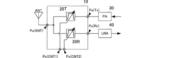
- FIG. 1 is a circuit configuration diagram of a high-frequency front end circuit 10 according to the present embodiment.
- the high-frequency front end circuit 10 includes variable filters 20T and 20R.
- the variable filter 20T corresponds to the first variable filter of the present invention
- the variable filter 20R corresponds to the second variable filter of the present invention.
- a case where the variable filter 20T is used as a transmission filter and the variable filter 20R is used as a reception filter for a specific communication signal (transmission signal and reception signal) is shown. Therefore, the variable filter 20T and the variable filter 20R constitute a variable duplexer.
- variable filters 20T and 20R have a configuration capable of adjusting the pass frequency band and the attenuation frequency band. Further, the variable filters 20T and 20R have a configuration capable of adjusting the impedance characteristics. For example, when the variable filters 20T and 20R are configured by an LC circuit composed of an inductor and a capacitor, a variable inductor capable of adjusting the inductance is used as a part of the inductor used, or a variable whose capacitance can be adjusted as a part of the capacitor used. Use capacitors.
- variable filters 20T and 20R may be provided in the variable filters 20T and 20R, so that an open state (corresponding to an open state of impedance) and a conductive state may be switched physically (mechanically).
- MEMS Micro-Electro-Mechanical Systems
- a control signal input terminal P M (CNT1) is connected to the variable filter 20T.
- the variable filter 20T can adjust the frequency characteristic and the impedance characteristic by the first control signal input from the control signal input terminal P M (CNT1).
- a control signal input terminal P M (CNT2) is connected to the variable filter 20R.
- the variable filter 20R can adjust the frequency characteristic and the impedance characteristic by the second control signal input from the control signal input terminal P M (CNT2).
- variable filters 20T and 20R are connected to a common terminal P M (ANT).
- a common antenna ANT is connected to the common terminal P M (ANT).
- the common antenna ANT transmits and receives specific communication signals to the outside.
- variable filter 20T The other end of the variable filter 20T is connected to the transmission-side individual terminal P M (Tx).
- the transmission-side individual terminal P M (Tx) is connected to the power amplifier (PA) 30.
- the power amplifier 30 amplifies the transmission signal of the specific communication signal and inputs it to the transmission-side individual terminal P M (Tx).
- the other end of the variable filter 20R is connected to the reception-side individual terminal P M (Rx).
- the reception-side individual terminal P M (Rx) is connected to the low noise amplifier (LNA) 40.
- the low noise amplifier 40 amplifies the received signal of the specific communication signal from the receiving-side individual terminal P M (Rx) and outputs the amplified signal to an external circuit.
- the high-frequency front end circuit 10 having such a configuration transmits and receives a specific communication signal by the following operation.
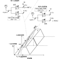
- FIG. 3 is a diagram showing a filter setting concept when transmitting / receiving an FDD communication signal.
- the variable filter 20T uses the first control signal so that the transmission frequency band is within the pass band and the reception frequency band is within the attenuation band. Bandwidth characteristics are set. Further, the band characteristics of the variable filter 20R are set so that the reception frequency band is in the pass band and the transmission frequency band is in the attenuation band. Such band setting of the variable filters 20T and 20R is maintained regardless of time during transmission and reception of FDD communication signals.
- the pass band of the variable filter 20T is adjusted to, for example, 1920 to 1980 MHz
- the pass band of the variable filter 20R is adjusted to, for example, 2110 to 2170 MHz.
- the transmission signal input from the transmission-side individual terminal P M (Tx) is subjected to filtering of unnecessary wave components by the variable filter 20T, and then passed through the common terminal P M (ANT). It is transmitted from the common antenna ANT.
- the transmission signal is attenuated by the variable filter 20R and is not propagated to the reception-side individual terminal P M (Rx).
- the received signal received by the common antenna ANT and input from the common terminal P M (ANT) is filtered from the unwanted wave component by the variable filter 20R and output from the reception-side individual terminal P M (Rx).
- the received signal is attenuated by the variable filter 20T and is not propagated to the transmission-side individual terminal P M (Tx).
- FDD communication signals having different transmission frequency bands and reception frequency bands can be transmitted and received by a single common antenna.
- FIG. 4 is a diagram showing a filter setting concept when transmitting / receiving a TDD communication signal. Note that FIG. 4 shows a case where the transmission frequency band and the reception frequency band completely match, but the present invention can also be applied to a case where the frequency bands overlap at least partially.
- variable filter 20T is set so that the transmission / reception frequency band of the communication signal is within the pass band when the variable filter 20T is transmitted.
- variable filter 20T for transmitting a TDD communication signal is set so that the transmission frequency band becomes the pass band during the transmission period (the period up to time tch in FIG. 4).
- the pass band of the variable filter 20T is set to, for example, 1900 to 1920 MHz.
- the variable filter 20R is set so that the impedance in the transmission / reception frequency band is open when the variable filter 20R side is viewed from the connection point of the variable filters 20T and 20R.
- the impedance of the variable filter 20R By setting the impedance of the variable filter 20R in this manner, the unnecessary signal component of the transmission signal input from the transmission-side individual terminal P M (Tx) is filtered by the variable filter 20T, and the common terminal P M It is transmitted from the common antenna ANT via (ANT). At this time, since the impedance on the receiving circuit side is set to be open with respect to the transmission signal, the transmission signal is not propagated to the variable filter 20R and the reception-side individual terminal P M (Rx).
- the reception frequency band of the variable filter 20R is set to be the pass band.
- the pass band of the variable filter 20R is set to, for example, 1900 to 1920 MHz.
- the impedance of the variable filter 20T is set so that the impedance in the transmission / reception frequency band is open when the variable filter 20T side is viewed from the connection point of the variable filters 20T and 20R.
- the reception signal received by the common antenna ANT and input from the common terminal P M (ANT) is subjected to unnecessary wave component filtering by the variable filter 20R. , And output from the receiving-side individual terminal P M (Rx).
- the reception signal is not propagated to the variable filter 20T and the transmission-side individual terminal P M (Tx).
- a TDD communication signal can be transmitted and received with a single common antenna.
- a high-frequency front-end circuit having a simple configuration using a common antenna, whether it is an FDD communication signal or a TDD communication signal, is used. You can send and receive.
- an FDD communication signal is transmitted and received and a case where a TDD communication signal is transmitted and received are individually described.
- the pass band of the variable filter 20T can be changed to the transmission frequency band of the FDD communication signal, and the pass band of the variable filter 20R can be changed to the reception frequency band of the FDD communication signal.
- the FDD communication signal and the TDD communication signal can be transmitted and received by the common high-frequency front-end circuit.
- a TDD communication signal can be transmitted and received by a common antenna without using a switch element.
- FIG. 5 is a circuit configuration diagram of the high-frequency front-end circuit 10A according to the present embodiment.
- the high-frequency front end circuit 10A includes variable duplexers 21L, 21M, and 21H. These variable duplexers 21L, 21M, and 21H have different ranges in which a pass band can be set.
- the frequency band of all communication signals used as the high-frequency front-end circuit 10A is set to a Low band, a Middle band, and a Hi band with reference to the frequency height.
- the variable duplexer 21L is set for the Low band
- the variable duplexer 21M is set for the Middle band
- the variable duplexer 21H is set for the Hi band.
- the variable duplexer 21L includes variable filters 20TL and 20RL.
- the common terminal of the variable duplexer 21L is connected to the common terminal P M (ANT) of the high-frequency front end circuit 10A.
- the variable filter 20TL side individual terminal of the variable duplexer 21L is connected to the first transmission side individual terminal P M (TxL) of the high-frequency front end circuit 10A.
- the variable filter 20RL side individual terminal of the variable duplexer 21L is connected to the first reception side individual terminal P M (RxL) of the high-frequency front end circuit 10A.
- the variable duplexer 21M includes variable filters 20TM and 20RM.
- the common terminal of the variable duplexer 21M is connected to the common terminal P M (ANT) of the high-frequency front end circuit 10A.
- the variable filter 20TM side individual terminal of the variable duplexer 21M is connected to the second transmission side individual terminal P M (TxM) of the high-frequency front end circuit 10A.
- the variable filter 20RM side individual terminal of the variable duplexer 21M is connected to the second reception side individual terminal P M (RxM) of the high frequency front end circuit 10A.
- the variable duplexer 21H includes variable filters 20TH and 20RH.
- the common terminal of the variable duplexer 21H is connected to the common terminal P M (ANT) of the high-frequency front end circuit 10A.
- the variable filter 20TH side individual terminal of the variable duplexer 21H is connected to the third transmission side individual terminal P M (TxH) of the high-frequency front end circuit 10A.
- the variable filter 20RH side individual terminal of the variable duplexer 21H is connected to the third reception side individual terminal P M (RxH) of the high-frequency front end circuit 10A.
- variable filter 20RL when a TDD transmission signal is input from the first transmission-side individual terminal P M (TxL), the variable filter 20RL is connected to the connection points (that is, the duplexer 21L) of the variable filters 20TL and 20RL.
- the impedance is set so that the impedance in the transmission / reception frequency band is open when the variable filter 20RL side is viewed from the common terminal).
- variable duplexers 21M and 21H retain their pass characteristics as long as the pass band of each filter does not match the band of the transmission signal input to the first transmission-side individual terminal P M (TxL). .
- the variable duplexer 21M is used in the matching band.
- 21H side (in particular, the variable duplexer 21M side having a similar operating frequency) is set so that the impedance is open.
- the impedance may be set to be open even if the passband of each filter does not match the band of the transmission signal input to the first receiving side individual terminal P M (RxL).
- a plurality of communication signals are transmitted and received by the common antenna ANT while ensuring isolation between the individual terminals. be able to. Furthermore, since the frequency range that can be processed is widened by adopting the configuration as in the present embodiment, it is possible to provide a front-end circuit that can cope with more frequency bands.
- 10, 10A, 10P high-frequency front end circuit
- 11 switch element
- 121, 122, 123, 124 SAW duplexer
- 21L, 21M, 21H Variable duplexer
- 30 Power amplifier (PA)
- 40 Low noise amplifier (LNA)
Landscapes
- Engineering & Computer Science (AREA)
- Computer Networks & Wireless Communication (AREA)
- Signal Processing (AREA)
- Transceivers (AREA)
Abstract
高周波フロントエンド回路(1)は、可変型フィルタ(20T)と可変型フィルタ(20R)を備える。可変型フィルタ(20T,20R)の一方端は共通端子(PM(ANT))に接続する。可変型フィルタ(20T)の他方端は送信側個別端子(PM(Tx))に接続し、可変型フィルタ(20R)の他方端は受信側個別端子(PM(Rx))に接続する。送信信号の伝送時、可変型フィルタ(20T,20R)の接続点から可変型フィルタ(20R)側を見たインピーダンスがオープンになるように、可変型フィルタ(20R)のインピーダンスを調整する。受信信号の伝送時、可変型フィルタ(20T,20R)の接続点から可変型フィルタ(20T)側を見たインピーダンスがオープンになるように、可変型フィルタ(20T)のインピーダンスを調整する。
Description
本発明は、通信仕様がそれぞれに異なる複数の通信信号を送受信する高周波フロントエンド回路に関する。
従来、それぞれに異なる周波数帯域利用した複数の通信信号を、共通アンテナで送受信するための高周波フロントエンド回路が各種考案されている。図1は従来の一般的な高周波フロントエンド回路10Pの回路構成図である。なお、図1に示す高周波フロントエンド回路は、四種類の通信信号を共通アンテナで送受信する例を示している。
従来の高周波フロントエンド回路10Pは、スイッチ素子11と、SAWデュプレクサ121,122,123,124を備える。スイッチ素子11は、共通端子PIC(ANT0)と、個別端子PIC(RF1)~個別端子PIC(RF4)を備える。スイッチ素子11は、駆動電源端子PIC(VDD)から入力される駆動電圧で起動し、複数の制御信号入力端子PIC(Vc)から入力される制御信号に基づいて、共通端子PIC(ANT0)に、個別端子PIC(RF1)~個別端子PIC(RF4)のいずれかを接続する。共通端子PIC(ANT0)には、共通アンテナANTが接続されている。
個別端子PIC(RF1)には、SAWデュプレクサ121が接続されている。SAWデュプレクサ121の送信側フィルタは第1送信信号入力端子PM(Tx1)に接続されている。SAWデュプレクサ121の受信側フィルタは第1受信信号出力端子PM(Rx1)に接続されている。
個別端子PIC(RF2)には、SAWデュプレクサ122が接続されている。SAWデュプレクサ122の送信側フィルタは第2送信信号入力端子PM(Tx2)に接続されている。SAWデュプレクサ122の受信側フィルタは第2受信信号出力端子PM(Rx2)に接続されている。
個別端子PIC(RF3)には、SAWデュプレクサ123が接続されている。SAWデュプレクサ123の送信側フィルタは第2送信信号入力端子PM(Tx3)に接続されている。SAWデュプレクサ123の受信側フィルタは第2受信信号出力端子PM(Rx3)に接続されている。
個別端子PIC(RF4)には、SAWデュプレクサ124が接続されている。SAWデュプレクサ124の送信側フィルタは第4送信信号入力端子PM(Tx4)に接続されている。SAWデュプレクサ124の受信側フィルタは第4受信信号出力端子PM(Rx4)に接続されている。
このような構成により、従来の高周波フロントエンド回路は、各送信信号入力端子からの送信信号を共通アンテナANTから送信し、共通アンテナANTで受信した受信信号を所望の受信信号出力端子から出力している。
ところで、現在、携帯電話の無線通信方式として、第三世代(3G)の携帯電話の3GPP(Third Generation Partnership Project)規格では、例えば、W-CDMA(Wide Band Code Division Multiple Access)、3GPP2(Third Generation Partnership ProjectThird Generation2)規格では、例えば、CDMA2000(Wide Band cdmaOne)がFDD(Frequency Division Duplex)方式であり、3GPP規格のGSM(Global System for Mobile Communications)、TD-LTE(Time Division Long Term Evolution)およびTD-SCDMA(Time Division Synchronous Code Division Multiple Access)がTDD(Time Division Duplex)方式である。
したがって、FDD方式の通信信号とTDD方式に対応した高周波フロントエンド回路が必要であり、このような高周波フロントエンド回路として、例えば、特許文献1には、FDD方式の通信信号と、TDD方式の通信信号とを、共通アンテナで送受信する高周波フロントエンド回路が記載されている。
特許文献1に記載の高周波フロントエンド回路は、当該特許文献1の図3にも記載されているように、FDD方式の通信信号を利用するための一つのポートと、TDD方式の通信信号を利用するための二つのポートが備えられており、伝送する通信信号に応じて、ポートを切り替えている。
しかしながら、上述のように、従来の高周波フロントエンド回路では、複数の通信信号(送信信号および受信信号)に対応するために、多分岐のスイッチ素子を用いたり、送信信号や受信信号の種類数に相当する数のデュプレクサを必要とする。このため、回路規模が大きくなったり、コストダウンが難しくなってしまうことがある。
また、従来の特許文献1に記載の構成は、TDD方式の通信信号に対する経路と、FDD方式の通信信号に対する経路とを、個別に備えなければならず、回路規模が大きくなってしまう。また、TDD方式の通信信号は、送信周波数帯域と受信周波数帯域とが重なり合うため、従来構成では、FDD方式の通信信号に対して利用可能なデュプレクサを利用することができず、必ずスイッチ素子を必要とし、この点においても、回路規模が大きくなったり、コストダウンが難しくなってしまう。
したがって、本発明の目的は、少ない回路構成であっても通信特性を低下させることなく、FDD方式の通信信号とTDD方式の通信信号の双方の通信信号を共通アンテナで送受信できる高周波フロントエンド回路を提供することにある。
この発明の高周波フロントエンド回路は、第1、第2可変型フィルタと、共通端子と、第1個別端子と、第2個別端子と、を備える。第1、第2可変型フィルタは、それぞれに通過特性およびインピーダンス特性を調整可能な構成からなる。共通端子は、第1可変型フィルタおよび第2可変型フィルタが接続されている。第1個別端子は、第1可変型フィルタの共通端子が接続される側と反対側に接続されている。第2個別端子は、第2可変型フィルタの共通端子が接続される側と反対側に接続されている。このような構成の上で、第1周波数帯域を利用した第1高周波信号を伝送する時には、第1可変型フィルタの通過帯域が第1周波数帯域に調整されるともに、共通端子側から見た前記第1周波数帯域での第2可変型フィルタのインピーダンスがオープンとなるように、第2可変型フィルタのインピーダンスが調整される。一方、第2周波数帯域を利用した第2高周波信号を伝送する時には、第2可変型フィルタの通過帯域が第2周波数帯域に調整されるともに、共通端子側から見た第2周波数帯域での第1可変型フィルタのインピーダンスがオープンとなるように、第1可変型フィルタのインピーダンスが調整される。
この構成では、第1高周波信号を伝送する時、例えば第1個別端子から第1高周波信号を入力して共通端子から出力する時には、第1可変型フィルタで第1高周波信号の不要波が減衰され共通端子から出力される。この際、第2可変型フィルタは、第1高周波信号の周波数に対してインピーダンスがオープンなので、第1高周波信号が第1可変型フィルタから第2可変型フィルタへ漏洩することを防止できる。一方、第2高周波信号伝送する場合、例えば共通端子から第2高周波信号を入力して第2個別端子から出力する時には、第2可変型フィルタで第2高周波信号の不要波が減衰され第2個別端子から出力される。この際、第1可変型フィルタは、第2高周波信号の周波数に対してインピーダンスがオープンなので、第2高周波信号が共通端子から第1可変型フィルタへ漏洩することを防止できる。すなわち、第1可変型フィルタ側と第2可変型フィルタ側との間のアイソレーションを確保することができ、通過帯域における信号のロスを少なくできる。
また、この発明の高周波フロントエンド回路は、第1可変型フィルタが特定の通信信号に対する送信側フィルタであり、第2可変型フィルタが特定の通信信号に対する受信側フィルタであり、共通端子が外部の共通アンテナに接続されるための端子であることが好ましい。
この構成では、特定の通信信号における送信回路と受信回路との間のアイソレーションを確保することができる。
また、この発明の高周波フロントエンド回路では、第1高周波信号の周波数と第2高周波信号の周波数とが少なくとも一部で重なっている時分割方式の通信信号に用いることが好ましい。
この構成では、本願発明の構成が有効に作用する周波数帯域が重なる場合を示しており、このような場合、フィルタ特性の設定だけではアイソレーションを確保できないが、上述のインピーダンス調整を行うことでアイソレーションを確保することができる。
また、この発明の高周波フロントエンド回路では、送信側フィルタと前記受信側フィルタとの組からなるデュプレクサを複数備え、各デュプレクサの共通端子が互いに接続されており、特定の通信信号を通過させるデュプレクサ以外のデュプレクサを構成する可変型フィルタは、該特定の通信信号に対するインピーダンスがオープンになるように、もしくは、該特定の通信信号の通過帯域が減衰帯域となるように調整されていることが好ましい。
この構成では、一種類の通信信号における送信信号および受信信号の送受信だけでなく、複数種類の通信信号を、各送信回路、受信回路間のアイソレーションを確保しながら、共通アンテナで送受信することができる。
また、この発明の高周波フロントエンド回路は、第1可変型フィルタおよび第2可変型フィルタが制御入力端子を備えることが好ましい。
この構成では、制御信号により各可変型フィルタの周波数特性やインピーダンス特性を調整する具体的な構成例を示している。
この発明によれば、少ない回路構成であっても通信特性を低下させることなく、FDD方式の通信信号、または、TDD方式の通信信号を含む複数の通信信号を共通アンテナで送受信することができる。
本発明の第1の実施形態に係る高周波フロントエンド回路について、図を参照して説明する。図1は本実施形態に係る高周波フロントエンド回路10の回路構成図である。
高周波フロントエンド回路10は、可変型フィルタ20T,20Rを備える。可変型フィルタ20Tは本発明の第1可変型フィルタに相当し、可変型フィルタ20Rは本発明の第2可変型フィルタに相当する。なお、本実施形態では、特定通信信号(送信信号および受信信号)に対して、可変型フィルタ20Tを送信側フィルタとして利用し、可変型フィルタ20Rを受信側フィルタとして利用する場合を示す。したがって、可変型フィルタ20Tと可変型フィルタ20Rとで可変型デュプレクサが構成される。
可変型フィルタ20T,20Rは、通過周波数帯域や減衰周波数帯域を調整可能な構成からなる。また、可変型フィルタ20T,20Rは、インピーダンス特性を調整可能な構成からなる。例えば、可変型フィルタ20T,20RをインダクタおよびキャパシタからなるLC回路から構成する場合、使用するインダクタの一部にインダクタンスを調整できる可変インダクタを用いたり、使用するキャパシタの一部にキャパシタンスを調整できる可変キャパシタを用いる。また、MEMS(Micro-Electro-Mechanical Systems)機構を可変型フィルタ20T,20Rに備え、物理的(機構的)に開放状態(インピーダンスがオープンの状態に相当)及び導通状態を切り替えるようにしてもよい。
可変型フィルタ20Tには、制御信号入力端子PM(CNT1)が接続されている。可変型フィルタ20Tは、制御信号入力端子PM(CNT1)から入力される第1制御信号により、周波数特性やインピーダンス特性を調整できる。
可変型フィルタ20Rには、制御信号入力端子PM(CNT2)が接続されている。可変型フィルタ20Rは、制御信号入力端子PM(CNT2)から入力される第2制御信号により、周波数特性やインピーダンス特性を調整できる。
可変型フィルタ20T,20Rの一方端は、共通端子PM(ANT)に接続されている。共通端子PM(ANT)は、共通アンテナANTが接続されている。共通アンテナANTは特定通信信号の外部に対する送受波を行う。
可変型フィルタ20Tの他方端は、送信側個別端子PM(Tx)に接続されている。送信側個別端子PM(Tx)は、パワーアンプ(PA)30に接続されている。パワーアンプ30は特定通信信号の送信信号の増幅処理を行い、送信側個別端子PM(Tx)へ入力させる。
可変型フィルタ20Rの他方端は、受信側個別端子PM(Rx)に接続されている。受信側個別端子PM(Rx)は、ローノイズアンプ(LNA)40に接続されている。ローノイズアンプ40は、受信側個別端子PM(Rx)からの特定通信信号の受信信号の増幅処理を行い、外部回路へ出力する。
このような構成からなる高周波フロントエンド回路10は、次に示すような動作により、特定通信信号の送受信を行う。
(1)特定通信信号として周波数分割(FDD)型の通信信号を送受信する場合
図3はFDD方式の通信信号を送受信する時のフィルタ設定概念を示す図である。
図3はFDD方式の通信信号を送受信する時のフィルタ設定概念を示す図である。
送信周波数と受信周波数とが異なるFDD方式の通信信号を送受信する場合、可変型フィルタ20Tは、第1制御信号により、送信周波数帯域が通過帯域内となり、受信周波数帯域が減衰帯域内となるように帯域特性が設定される。また、可変型フィルタ20Rは、受信周波数帯域が通過帯域内となり、送信周波数帯域が減衰帯域内となるように帯域特性が設定される。このような可変型フィルタ20T,20Rの帯域設定は、FDD方式の通信信号を送受信する間、時間に無関係に維持される。FDD方式にて通信を行うW-CDMAの場合、可変フィルタ20Tの通過帯域は、例えば、1920~1980MHzに調整され、可変フィルタ20Rの通過帯域は、例えば、2110~2170MHzに調整される。
このような構成とすることで、送信側個別端子PM(Tx)から入力された送信信号は、可変型フィルタ20Tで不要波成分がフィルタ処理されて、共通端子PM(ANT)を介して共通アンテナANTから送信される。この際、受信回路側においては、送信信号は、可変型フィルタ20Rで減衰されて受信側個別端子PM(Rx)には伝搬されない。
一方、共通アンテナANTで受信し、共通端子PM(ANT)から入力された受信信号は、可変型フィルタ20Rで不要波成分がフィルタ処理されて、受信側個別端子PM(Rx)から出力される。この際、送信回路側においては、受信信号は、可変型フィルタ20Tで減衰されて送信側個別端子PM(Tx)には伝搬されない。
このように、本実施形態の構成を用いれば、送信周波数帯域と受信周波数帯域とが異なるFDD方式の通信信号を、単一の共通アンテナで送受信することができる。
(2)特定通信信号としてTDD方式の通信信号を送受信する場合
図4はTDD方式の通信信号を送受信する時のフィルタ設定概念を示す図である。なお、図4では、送信周波数帯域と受信周波数帯域とが完全に一致する場合を示しているが、少なくも一部で周波数帯域が重なるような場合でも適用できる。
図4はTDD方式の通信信号を送受信する時のフィルタ設定概念を示す図である。なお、図4では、送信周波数帯域と受信周波数帯域とが完全に一致する場合を示しているが、少なくも一部で周波数帯域が重なるような場合でも適用できる。
また、以下の説明では、既定の設定として、可変型フィルタ20Tは送信時に、可変型フィルタ20Rはともに、通信信号の送受信周波数帯域が通過帯域内となるように設定される。
(2-1)送信期間
TDD方式の通信信号を送信するための可変型フィルタ20Tは、送信期間(図4における時刻tchまでの期間)中、送信周波数帯域が通過帯域となるように設定される。例えば、TDD方式にて通信を行うTD-LTEの場合は、可変型フィルタ20Tの通過帯域は、例えば、1900~1920MHzに設定される。一方で、可変型フィルタ20Rは送信期間中、可変型フィルタ20T,20Rの接続点から可変型フィルタ20R側を見て、送受信周波数帯域でのインピーダンスがオープンになるように、インピーダンスが設定される。
TDD方式の通信信号を送信するための可変型フィルタ20Tは、送信期間(図4における時刻tchまでの期間)中、送信周波数帯域が通過帯域となるように設定される。例えば、TDD方式にて通信を行うTD-LTEの場合は、可変型フィルタ20Tの通過帯域は、例えば、1900~1920MHzに設定される。一方で、可変型フィルタ20Rは送信期間中、可変型フィルタ20T,20Rの接続点から可変型フィルタ20R側を見て、送受信周波数帯域でのインピーダンスがオープンになるように、インピーダンスが設定される。
このように可変型フィルタ20Rのインピーダンスを設定することで、送信側個別端子PM(Tx)から入力された送信信号は、可変型フィルタ20Tで不要波成分がフィルタ処理されて、共通端子PM(ANT)を介して共通アンテナANTから送信される。この際、受信回路側のインピーダンスは、送信信号に対してオープンに設定されているので、送信信号は、可変型フィルタ20Rおよび受信側個別端子PM(Rx)には伝搬されない。
(2-2)受信期間
一方、受信期間(図4における時刻tch以降の期間)中においては、可変型フィルタ20Rの受信周波数帯域が通過帯域となるように設定される。例えば、TDD方式にて通信を行うTD-LTEの場合、可変型フィルタ20Rの通過帯域は、例えば、1900~1920MHzに設定される。一方で、可変型フィルタ20Tは、可変型フィルタ20T,20Rの接続点から可変型フィルタ20T側を見て、送受信周波数帯域でのインピーダンスがオープンになるように、インピーダンスが設定される。
一方、受信期間(図4における時刻tch以降の期間)中においては、可変型フィルタ20Rの受信周波数帯域が通過帯域となるように設定される。例えば、TDD方式にて通信を行うTD-LTEの場合、可変型フィルタ20Rの通過帯域は、例えば、1900~1920MHzに設定される。一方で、可変型フィルタ20Tは、可変型フィルタ20T,20Rの接続点から可変型フィルタ20T側を見て、送受信周波数帯域でのインピーダンスがオープンになるように、インピーダンスが設定される。
このように可変型フィルタ20Tのインピーダンスを設定することで、共通アンテナANTで受信し、共通端子PM(ANT)から入力された受信信号は、可変型フィルタ20Rで不要波成分がフィルタ処理されて、受信側個別端子PM(Rx)から出力される。この際、送信回路側のインピーダンスは、受信信号に対してオープンに設定されているので、受信信号は、可変型フィルタ20Tおよび送信側個別端子PM(Tx)には伝搬されない。
このように、本実施形態の構成を用いれば、TDD方式の通信信号を、単一の共通アンテナで送受信することができる。
以上のように、本実施形態の構成を用いれば、FDD方式の通信信号であっても、TDD方式の通信信号であっても、共通のアンテナを用い、簡素な構成からなる高周波フロントエンド回路で送受信することができる。
なお、上述の説明では、FDD方式の通信信号を送受信する場合とTDD方式の通信信号を送受信する場合を個別に説明した。しかしながら、例えば、既定の設定として、上述のTDDの送受信周波数帯域に、可変型フィルタ20T,20Rの通過帯域を設定しておき、FDD方式の通信信号の送受信を行う制御が入力された際に、可変型フィルタ20Tの通過帯域をFDD方式の通信信号の送信周波数帯域に変更し、可変型フィルタ20Rの通過帯域をFDD方式の通信信号の受信周波数帯域に変更するように設定することもできる。これにより、FDD方式の通信信号とTDD方式の通信信号とを共通の高周波フロントエンド回路で送受信することができる。さらに、スイッチ素子を用いずにTDD方式の通信信号を共通アンテナで送受信処理することができる。
次に、第2の実施形態に係る高周波フロントエンド回路について、図を参照して説明する。図5は本実施形態に係る高周波フロントエンド回路10Aの回路構成図である。
上述の第1の実施形態では送信側フィルタと受信側フィルタとの組を一組設けた場合を示したが、本実施形態では送信側フィルタと受信側フィルタとの組を複数設けている。
高周波フロントエンド回路10Aは、可変型デュプレクサ21L,21M,21Hを備える。これら可変型デュプレクサ21L,21M,21Hは通過帯域を設定可能な範囲が異なるものである。例えば、高周波フロントエンド回路10Aとして使用した全通信信号の周波数帯域を、周波数の高さを基準に、Lowバンド、Middleバンド、Hiバンドに設定する。そして、可変型デュプレクサ21LをLowバンド用に、可変型デュプレクサ21MをMiddleバンド用に、可変型デュプレクサ21HをHiバンド用に、それぞれ設定する。
可変型デュプレクサ21Lは、可変型フィルタ20TL,20RLからなる。可変型デュプレクサ21Lの共通端子は、高周波フロントエンド回路10Aの共通端子PM(ANT)に接続されている。可変型デュプレクサ21Lの可変型フィルタ20TL側個別端子は、高周波フロントエンド回路10Aの第1送信側個別端子PM(TxL)に接続されている。可変型デュプレクサ21Lの可変型フィルタ20RL側個別端子は、高周波フロントエンド回路10Aの第1受信側個別端子PM(RxL)に接続されている。
可変型デュプレクサ21Mは、可変型フィルタ20TM,20RMからなる。可変型デュプレクサ21Mの共通端子は、高周波フロントエンド回路10Aの共通端子PM(ANT)に接続されている。可変型デュプレクサ21Mの可変型フィルタ20TM側個別端子は、高周波フロントエンド回路10Aの第2送信側個別端子PM(TxM)に接続されている。可変型デュプレクサ21Mの可変型フィルタ20RM側個別端子は、高周波フロントエンド回路10Aの第2受信側個別端子PM(RxM)に接続されている。
可変型デュプレクサ21Hは、可変型フィルタ20TH,20RHからなる。可変型デュプレクサ21Hの共通端子は、高周波フロントエンド回路10Aの共通端子PM(ANT)に接続されている。可変型デュプレクサ21Hの可変型フィルタ20TH側個別端子は、高周波フロントエンド回路10Aの第3送信側個別端子PM(TxH)に接続されている。可変型デュプレクサ21Hの可変型フィルタ20RH側個別端子は、高周波フロントエンド回路10Aの第3受信側個別端子PM(RxH)に接続されている。
このような構成では、例えば、第1送信側個別端子PM(TxL)からTDD方式の送信信号が入力されると、可変型フィルタ20RLは、可変型フィルタ20TL,20RLの接続点(すなわちデュプレクサ21Lの共通端子)から可変型フィルタ20RL側を見て、送受信周波数帯域でのインピーダンスがオープンになるように、インピーダンスが設定される。
また、可変型デュプレクサ21M,21Hは、各フィルタの通過帯域が、第1送信側個別端子PM(TxL)に入力された送信信号の帯域と一致しなければ、そのままの通過特性が保持される。ここで、各フィルタの通過帯域が、第1送信側個別端子PM(TxL)に入力された送信信号の帯域と部分的に一致することがあれば、当該一致する帯域において、可変型デュプレクサ21M,21H側(特に、使用周波数の近い可変型デュプレクサ21M側)を見たインピーダンスがオープンになるように設定する。もちろん、各フィルタの通過帯域が、第1受信側個別端子PM(RxL)に入力された送信信号の帯域と一致しなくても、インピーダンスをオープンに設定してもよい。
このように、複数のデュプレクサ(送信側フィルタと受信側フィルタとの組)を用いる構成であっても、各個別端子間のアイソレーションを確保しながら、共通アンテナANTで複数の通信信号を送受信することができる。さらに、本実施形態のような構成とすることで、処理できる周波数範囲が広がるので、より多くの周波数帯域に対応できるフロントエンド回路を提供できるようになる。
10,10A,10P:高周波フロントエンド回路、11:スイッチ素子、121,122,123,124:SAWデュプレクサ、
20T,20R,20TL,20RL,20TM,20RM,20TH,20RH:可変型フィルタ、21L,21M,21H:可変型デュプレクサ、30:パワーアンプ(PA)、40:ローノイズアンプ(LNA)
20T,20R,20TL,20RL,20TM,20RM,20TH,20RH:可変型フィルタ、21L,21M,21H:可変型デュプレクサ、30:パワーアンプ(PA)、40:ローノイズアンプ(LNA)
Claims (5)
- 通過特性およびインピーダンス特性を調整可能な第1、第2可変型フィルタと、
前記第1可変型フィルタおよび前記第2可変型フィルタが接続される共通端子と、
前記第1可変型フィルタの前記共通端子が接続される側と反対側に接続された第1個別端子と、
前記第2可変型フィルタの前記共通端子が接続される側と反対側に接続された第2個別端子と、を備え、
第1周波数帯域を利用した第1高周波信号を伝送する時には、前記第1可変型フィルタの通過帯域が前記第1周波数帯域に調整されるともに、前記共通端子側から見た前記第1周波数帯域での前記第2可変型フィルタのインピーダンスがオープンとなるように、前記第2可変型フィルタのインピーダンスが調整され、
第2周波数帯域を利用した第2高周波信号を伝送する時には、前記第2可変型フィルタの通過帯域が前記第2周波数帯域に調整されるともに、前記共通端子側から見た前記第2周波数帯域での前記第1可変型フィルタのインピーダンスがオープンとなるように、前記第1可変型フィルタのインピーダンスが調整される、高周波フロントエンド回路。 - 前記第1可変型フィルタは特定の通信信号に対する送信側フィルタであり、
前記第2可変型フィルタは前記特定の通信信号に対する受信側フィルタであり、
前記共通端子は、外部の共通アンテナに接続されるための端子である、請求項1に記載の高周波フロントエンド回路。 - 前記特定の通信信号は、前記第1高周波信号の周波数と前記第2高周波信号の周波数とが少なくとも一部で重なっている、時分割方式の通信信号である、請求項1または請求項2に記載の高周波フロントエンド回路。
- 前記送信側フィルタと前記受信側フィルタとの組からなるデュプレクサを複数備え、
各デュプレクサの共通端子が互いに接続されており、
前記特定の通信信号を通過させるデュプレクサ以外のデュプレクサを構成する可変型フィルタは、該特定の通信信号に対するインピーダンスがオープンになるように、もしくは、該特定の通信信号の通過帯域が減衰帯域となるように調整されている、請求項2または請求項3に記載の高周波フロントエンド回路。 - 前記第1可変型フィルタおよび前記第2可変型フィルタは制御入力端子を備える、請求項1乃至請求項4のいずれかに記載の高周波フロントエンド回路。
Priority Applications (2)
| Application Number | Priority Date | Filing Date | Title |
|---|---|---|---|
| CN201280014680.1A CN103460611B (zh) | 2011-04-14 | 2012-03-01 | 高频前端电路 |
| US14/050,406 US9287918B2 (en) | 2011-04-14 | 2013-10-10 | High-frequency front-end circuit |
Applications Claiming Priority (2)
| Application Number | Priority Date | Filing Date | Title |
|---|---|---|---|
| JP2011-089749 | 2011-04-14 | ||
| JP2011089749 | 2011-04-14 |
Related Child Applications (1)
| Application Number | Title | Priority Date | Filing Date |
|---|---|---|---|
| US14/050,406 Continuation US9287918B2 (en) | 2011-04-14 | 2013-10-10 | High-frequency front-end circuit |
Publications (1)
| Publication Number | Publication Date |
|---|---|
| WO2012140969A1 true WO2012140969A1 (ja) | 2012-10-18 |
Family
ID=47009151
Family Applications (1)
| Application Number | Title | Priority Date | Filing Date |
|---|---|---|---|
| PCT/JP2012/055182 Ceased WO2012140969A1 (ja) | 2011-04-14 | 2012-03-01 | 高周波フロントエンド回路 |
Country Status (3)
| Country | Link |
|---|---|
| US (1) | US9287918B2 (ja) |
| CN (1) | CN103460611B (ja) |
| WO (1) | WO2012140969A1 (ja) |
Cited By (7)
| Publication number | Priority date | Publication date | Assignee | Title |
|---|---|---|---|---|
| WO2014167963A1 (ja) * | 2013-04-12 | 2014-10-16 | 株式会社Nttドコモ | 移動通信機器 |
| WO2015086065A1 (en) * | 2013-12-11 | 2015-06-18 | Epcos Ag | Front end circuit and method of operating a front end circuit |
| CN105379129A (zh) * | 2013-07-16 | 2016-03-02 | 株式会社村田制作所 | 前端电路 |
| CN105474537A (zh) * | 2013-05-29 | 2016-04-06 | 诺基亚技术有限公司 | 用于可调谐umts多频段滤波器的频段分组组合 |
| WO2016129401A1 (ja) * | 2015-02-13 | 2016-08-18 | 株式会社 村田製作所 | 送受信モジュール |
| JP2017512019A (ja) * | 2014-02-28 | 2017-04-27 | エプコス アクチエンゲゼルシャフトEpcos Ag | フロントエンド回路 |
| CN110022160A (zh) * | 2017-12-07 | 2019-07-16 | 英飞凌科技股份有限公司 | 用于射频滤波器的系统和方法 |
Families Citing this family (10)
| Publication number | Priority date | Publication date | Assignee | Title |
|---|---|---|---|---|
| JP2015204604A (ja) * | 2014-04-16 | 2015-11-16 | シャープ株式会社 | 通信回路および電子機器 |
| US9432852B2 (en) | 2014-09-26 | 2016-08-30 | Cellphone-Mate, Inc. | Apparatus and methods for radio frequency signal boosters for cellular and broadcast television signals with Wi-Fi signals transmission function |
| WO2016104234A1 (ja) * | 2014-12-26 | 2016-06-30 | 株式会社村田製作所 | 高周波フロントエンド回路および通信装置 |
| US9775051B2 (en) | 2015-01-02 | 2017-09-26 | Cellphone-Mate, Inc. | Apparatus and methods for radio frequency signal boosters |
| JP2018514023A (ja) * | 2015-03-17 | 2018-05-31 | アマゾン テクノロジーズ インコーポレイテッド | コンテンツ・デプロイメント、スケーリングおよびテレメトリ |
| JP6411398B2 (ja) | 2016-03-14 | 2018-10-24 | 太陽誘電株式会社 | フィルタ回路、フロントエンド回路およびモジュール |
| JP6790447B2 (ja) * | 2016-05-12 | 2020-11-25 | 株式会社村田製作所 | スイッチモジュール |
| WO2017215634A1 (en) | 2016-06-17 | 2017-12-21 | Cellphone-Mate, Inc. | Radio frequency signal boosters for vehicles |
| WO2019032813A1 (en) | 2017-08-11 | 2019-02-14 | Cellphone-Mate, Inc. | RADIO FREQUENCY SIGNAL AMPLIFIER FOR VEHICLES |
| EP4122103B1 (en) * | 2020-06-12 | 2025-12-03 | Huawei Technologies Co., Ltd. | Receiver unit, device with receiver unit, and method for suppressing interference |
Citations (5)
| Publication number | Priority date | Publication date | Assignee | Title |
|---|---|---|---|---|
| JPH0851381A (ja) * | 1994-08-04 | 1996-02-20 | Uniden Corp | 集積化が可能な高周波用ポート選択回路 |
| JPH1146102A (ja) * | 1997-05-30 | 1999-02-16 | Murata Mfg Co Ltd | 誘電体フィルタ、誘電体デュプレクサ及び通信機装置 |
| JPH11243304A (ja) * | 1997-03-12 | 1999-09-07 | Matsushita Electric Ind Co Ltd | アンテナ共用器 |
| JP2002208802A (ja) * | 2001-01-11 | 2002-07-26 | Nikko Co | 帯域可変型フィルタ回路及びそれを用いた高周波フロントエンド回路 |
| JP2003133989A (ja) * | 2001-08-10 | 2003-05-09 | Hitachi Metals Ltd | マルチバンドアンテナスイッチ回路及びマルチバンドアンテナスイッチ積層モジュール複合部品並びにこれを用いた通信装置 |
Family Cites Families (5)
| Publication number | Priority date | Publication date | Assignee | Title |
|---|---|---|---|---|
| JP3393954B2 (ja) | 1995-05-16 | 2003-04-07 | 松下電器産業株式会社 | 時分割多重fdd/tddデュアルモード無線機 |
| DE69834679T2 (de) * | 1997-03-12 | 2006-09-21 | Matsushita Electric Industrial Co., Ltd., Kadoma | Antennenweiche |
| US7057472B2 (en) | 2001-08-10 | 2006-06-06 | Hitachi Metals, Ltd. | Bypass filter, multi-band antenna switch circuit, and layered module composite part and communication device using them |
| US7212789B2 (en) * | 2002-12-30 | 2007-05-01 | Motorola, Inc. | Tunable duplexer |
| US7446629B2 (en) * | 2004-08-04 | 2008-11-04 | Matsushita Electric Industrial Co., Ltd. | Antenna duplexer, and RF module and communication apparatus using the same |
-
2012
- 2012-03-01 CN CN201280014680.1A patent/CN103460611B/zh active Active
- 2012-03-01 WO PCT/JP2012/055182 patent/WO2012140969A1/ja not_active Ceased
-
2013
- 2013-10-10 US US14/050,406 patent/US9287918B2/en active Active
Patent Citations (5)
| Publication number | Priority date | Publication date | Assignee | Title |
|---|---|---|---|---|
| JPH0851381A (ja) * | 1994-08-04 | 1996-02-20 | Uniden Corp | 集積化が可能な高周波用ポート選択回路 |
| JPH11243304A (ja) * | 1997-03-12 | 1999-09-07 | Matsushita Electric Ind Co Ltd | アンテナ共用器 |
| JPH1146102A (ja) * | 1997-05-30 | 1999-02-16 | Murata Mfg Co Ltd | 誘電体フィルタ、誘電体デュプレクサ及び通信機装置 |
| JP2002208802A (ja) * | 2001-01-11 | 2002-07-26 | Nikko Co | 帯域可変型フィルタ回路及びそれを用いた高周波フロントエンド回路 |
| JP2003133989A (ja) * | 2001-08-10 | 2003-05-09 | Hitachi Metals Ltd | マルチバンドアンテナスイッチ回路及びマルチバンドアンテナスイッチ積層モジュール複合部品並びにこれを用いた通信装置 |
Cited By (15)
| Publication number | Priority date | Publication date | Assignee | Title |
|---|---|---|---|---|
| WO2014167963A1 (ja) * | 2013-04-12 | 2014-10-16 | 株式会社Nttドコモ | 移動通信機器 |
| JP2014207552A (ja) * | 2013-04-12 | 2014-10-30 | 株式会社Nttドコモ | 移動通信機器 |
| CN105474537B (zh) * | 2013-05-29 | 2019-09-27 | 起源资产集团有限责任公司 | 用于可调谐umts多频段滤波器的频段分组组合 |
| CN105474537A (zh) * | 2013-05-29 | 2016-04-06 | 诺基亚技术有限公司 | 用于可调谐umts多频段滤波器的频段分组组合 |
| JP2016523064A (ja) * | 2013-05-29 | 2016-08-04 | ノキア テクノロジーズ オーユー | チューナブルumtsマルチバンドフィルタのためのバンドグループ化の組み合せ |
| CN105379129A (zh) * | 2013-07-16 | 2016-03-02 | 株式会社村田制作所 | 前端电路 |
| US9979419B2 (en) | 2013-07-16 | 2018-05-22 | Murata Manufacturing Co., Ltd. | Front-end circuit |
| US9948327B2 (en) | 2013-12-11 | 2018-04-17 | Snaptrack, Inc. | Front end circuit and method of operating a front end circuit |
| JP2017503401A (ja) * | 2013-12-11 | 2017-01-26 | エプコス アクチエンゲゼルシャフトEpcos Ag | フロントエンド回路およびフロントエンド回路の動作の方法 |
| WO2015086065A1 (en) * | 2013-12-11 | 2015-06-18 | Epcos Ag | Front end circuit and method of operating a front end circuit |
| JP2017512019A (ja) * | 2014-02-28 | 2017-04-27 | エプコス アクチエンゲゼルシャフトEpcos Ag | フロントエンド回路 |
| US10277259B2 (en) | 2014-02-28 | 2019-04-30 | Snaptrack, Inc. | Front-end circuit for simultaneous transmission and reception operation |
| WO2016129401A1 (ja) * | 2015-02-13 | 2016-08-18 | 株式会社 村田製作所 | 送受信モジュール |
| US10623171B2 (en) | 2015-02-13 | 2020-04-14 | Murata Manufacturing Co., Ltd. | Transmission and reception module for a plurality of frequency bands |
| CN110022160A (zh) * | 2017-12-07 | 2019-07-16 | 英飞凌科技股份有限公司 | 用于射频滤波器的系统和方法 |
Also Published As
| Publication number | Publication date |
|---|---|
| US9287918B2 (en) | 2016-03-15 |
| US20140038531A1 (en) | 2014-02-06 |
| CN103460611B (zh) | 2015-08-19 |
| CN103460611A (zh) | 2013-12-18 |
Similar Documents
| Publication | Publication Date | Title |
|---|---|---|
| WO2012140969A1 (ja) | 高周波フロントエンド回路 | |
| CN110048735B (zh) | 用于射频滤波器的系统和方法 | |
| EP2911305B1 (en) | Multiplexer | |
| US9231552B2 (en) | RF front-end module and mobile wireless terminal | |
| CN105099493B (zh) | 射频电路和移动终端 | |
| JP5725186B2 (ja) | 高周波フロントエンドモジュール | |
| US10236925B2 (en) | High frequency front-end circuit and communication device | |
| CN107852188A (zh) | 前端模块 | |
| KR101945798B1 (ko) | 고주파 프런트엔드 회로 | |
| CN110601676A (zh) | 多路复用器和通信装置 | |
| CN113557671A (zh) | 多工器、高频模块以及通信装置 | |
| JP6428184B2 (ja) | 高周波フロントエンド回路、高周波モジュール | |
| US11881844B2 (en) | Multiplexer | |
| US9768838B2 (en) | Reconfigurable RF receive diplexer | |
| US9929752B2 (en) | RF receive diplexer | |
| US8976707B2 (en) | Radio-frequency front-end module | |
| US20150263405A1 (en) | Rf triplexer architecture | |
| HK1224440A1 (zh) | 高频滤波器 |
Legal Events
| Date | Code | Title | Description |
|---|---|---|---|
| 121 | Ep: the epo has been informed by wipo that ep was designated in this application |
Ref document number: 12771211 Country of ref document: EP Kind code of ref document: A1 |
|
| NENP | Non-entry into the national phase |
Ref country code: DE |
|
| 122 | Ep: pct application non-entry in european phase |
Ref document number: 12771211 Country of ref document: EP Kind code of ref document: A1 |
|
| NENP | Non-entry into the national phase |
Ref country code: JP |