WO2012133507A1 - 有機半導体デバイスおよび電極膜 - Google Patents
有機半導体デバイスおよび電極膜 Download PDFInfo
- Publication number
- WO2012133507A1 WO2012133507A1 PCT/JP2012/058093 JP2012058093W WO2012133507A1 WO 2012133507 A1 WO2012133507 A1 WO 2012133507A1 JP 2012058093 W JP2012058093 W JP 2012058093W WO 2012133507 A1 WO2012133507 A1 WO 2012133507A1
- Authority
- WO
- WIPO (PCT)
- Prior art keywords
- organic
- layer
- electrode layer
- ratio
- semiconductor device
- Prior art date
- Legal status (The legal status is an assumption and is not a legal conclusion. Google has not performed a legal analysis and makes no representation as to the accuracy of the status listed.)
- Ceased
Links
Images



Classifications
-
- H—ELECTRICITY
- H10—SEMICONDUCTOR DEVICES; ELECTRIC SOLID-STATE DEVICES NOT OTHERWISE PROVIDED FOR
- H10K—ORGANIC ELECTRIC SOLID-STATE DEVICES
- H10K50/00—Organic light-emitting devices
- H10K50/80—Constructional details
- H10K50/805—Electrodes
- H10K50/82—Cathodes
- H10K50/826—Multilayers, e.g. opaque multilayers
Definitions
- the present invention relates to an organic semiconductor device and an electrode film, and more particularly to an organic semiconductor device and an electrode film suitable for an organic electroluminescence element (organic EL element), an organic thin film solar cell, and the like.
- organic EL element organic electroluminescence element
- organic semiconductor devices using organic substances as semiconductor devices are known.
- this type of organic semiconductor device includes an organic electroluminescence element (organic EL element) using an organic material as a light emitting material, an organic thin film solar cell using an organic material combined with a conductive polymer, fullerene, or the like.
- organic EL element organic electroluminescence element
- organic thin film solar cell using an organic material combined with a conductive polymer, fullerene, or the like.
- Patent Document 1 discloses a positive electrode substrate in which a positive electrode layer (ITO layer or the like) and an organic material layer including a light emitting layer are laminated on the surface of a transparent substrate, and a negative electrode layer (on the surface of a resin film).
- An organic EL element is disclosed in which a negative electrode film on which a Mg—Ag alloy or the like is laminated is superposed on each other and heated and pressed to bond them together.
- This document describes that the emission characteristics can be improved by providing an electron injection layer (an alkali metal compound such as LiF) on the organic layer side of the negative electrode layer.
- an electron injection layer an alkali metal compound such as LiF
- Patent Document 2 discloses an organic EL element formed by sequentially laminating an anode, a hole injection layer, a light emitting layer, a cathode layer, and an oxide insulating layer on an insulating substrate. And the point which comprised the cathode layer from the two-layer structure of the Al layer (light emitting layer side) in which Ca exists and the Al layer (on the opposite side to the light emitting layer) in which Ca does not exist is described, for example.
- JP 2005-38816 A Japanese Patent No. 413336
- the electron injection layer for improving the light emission characteristics is formed as a layer different from the negative electrode layer. For this reason, an interface is formed between the electron injection layer and the negative electrode layer, and a contact resistance is generated between the electron injection layer and the negative electrode layer. Since the organic EL element is current-driven, there arises a problem that the drive voltage becomes high due to the contact resistance.
- the organic thin film solar cell includes a positive electrode layer on one surface of an organic material layer (photoelectric conversion layer) containing a conductive organic polymer as a photoelectric conversion material and a negative electrode layer on the other surface.
- a buffer layer made of an alkali metal or the like is provided on the organic layer side.
- the organic thin film solar cell when the buffer layer and the negative electrode layer are formed as separate layers, an interface is formed between the buffer layer and the negative electrode layer, and the contact resistance between the buffer layer and the negative electrode layer. Occurs. Since the organic thin-film solar cell is current-driven, there is a problem that the power generation amount or the extraction current efficiency is lowered due to the contact resistance.
- a problem to be solved by the present invention is to provide an organic semiconductor device and an electrode film capable of improving performance while suppressing problems caused by contact resistance.
- an organic semiconductor device includes a first electrode layer on one surface of an organic material layer of an organic semiconductor and a second electrode layer on the other surface, and the second electrode layer has a volume Highly conductive metal having a resistivity of 3.0 ⁇ 10 ⁇ 6 ⁇ ⁇ cm or less, alkaline earth metal, alkali metal, alkaline earth metal halide, alkali metal halide, Co oxide, Cu oxidation
- One or more charge transport materials selected from the group consisting of metal oxides, Mo oxides, Ni oxides, amine organic compounds, hydrazone organic compounds, stilbene organic compounds, starbust organic compounds, and phthalocyanine organic compounds Are formed directly on the other surface of the organic layer by co-evaporation, and the ratio of the high electrical conductivity metal in the second electrode layer is the organic content of the second electrode layer.
- the layer side becomes smaller than the ratio of the charge transport material and the second electrode layer on the side opposite to the organic material layer becomes larger than
- the ratio of the high electrical conductivity metal on the organic layer side of the second electrode layer is 30% or less, and the ratio of the high electrical conductivity metal on the side opposite to the organic layer of the second electrode layer is 70%. % Or more is preferable.
- the ratio of the highly electrically conductive metal is 30% or less within the range of at least 10 nm inward from the organic layer side surface of the second electrode layer.
- the ratio of the highly electrically conductive metal is 70% or more within a range of at least 10 nm inward from the surface opposite to the organic layer of the second electrode layer.
- the high electrical conductivity metal is preferably one or more metals selected from Al, Ag, Au, and Cu.
- the second electrode layer is preferably formed directly on the other surface of the organic layer by co-evaporation of Al and Ca or co-evaporation of Ag and Mg.
- an electrode film according to the present invention is an electrode film used for an electrode layer of an organic semiconductor device, and has a high electrical conductivity metal having a volume resistivity of 3.0 ⁇ 10 ⁇ 6 ⁇ ⁇ cm or less, alkaline earth Metal, alkali metal, alkaline earth metal halide, alkali metal halide, Co oxide, Cu oxide, Mo oxide, Ni oxide, amine organic compound, hydrazone organic compound, stilbene organic compound , One or more charge transport materials selected from the group consisting of a starbust organic compound and a phthalocyanine organic compound, wherein the ratio of the highly conductive metal is It is smaller than the ratio of the charge transport material and rises from one side to the other side so as to be larger than the ratio of the charge transport material on the other side. It is an gist and.
- the second electrode layer is directly formed on the other surface of the organic material layer by co-evaporation of a highly electrically conductive metal and a charge transport material, so that it is possible to suppress problems due to contact resistance.
- the performance can be improved.
- the ratio of the high electrical conductivity metal is made smaller than the ratio of the charge transport material on the organic layer side of the second electrode layer, the electron injection property by the charge transport material can be improved.
- the ratio of the high electrical conductivity metal is made larger than the ratio of the charge transport material on the side of the second electrode layer opposite to the organic material layer, the oxidative degradation of the charge transport material can be suppressed, and the degradation of the second electrode layer. Prevention can be achieved.
- the organic semiconductor device according to the present invention when applied to, for example, an organic EL element, the light emission efficiency can be improved as compared with the conventional case.
- improvement in power generation characteristics can be expected as compared with the conventional case.
- the ratio of the highly conductive metal on the organic layer side of the second electrode layer is 30% or less, the effect of improving the charge injection property by the charge transport material is excellent.
- the ratio of the highly electroconductive metal on the side of the second electrode layer opposite to the organic layer is 70% or more, the effect of suppressing the deterioration of the second electrode layer due to the oxidative deterioration of the charge transport material is excellent.
- the second electrode layer is formed by co-evaporation of Al and Ca or co-evaporation of Ag and Mg, the effect of improving the performance is suppressed while suppressing problems due to contact resistance.
- the ratio of the high electrical conductivity metal can be extremely reduced on the organic layer side of the second electrode layer, and the high electrical conductivity on the opposite side of the second electrode layer to the organic layer. Since the ratio of the conductive metal can be increased to nearly 100%, it is particularly effective for improving the charge injection property by the charge transport material and preventing the deterioration of the second electrode layer.
- Al as the cathode metal of the organic EL element and causing Ca to function as an electron injection material for the organic EL element, an organic EL element having excellent light emission characteristics can be obtained.
- the electrode film according to the present invention is formed by co-evaporation of a highly electrically conductive metal and a charge transport material, and the ratio of the highly electrically conductive metal is smaller than the ratio of the charge transport material on one side. Since it rises from the one side to the other side so that it is larger than the ratio of the charge transport material on the other side, there is a problem due to contact resistance when used for the electrode layer of an organic semiconductor device.
- the performance of the organic semiconductor device can be improved while suppressing the above. At this time, on one side, the charge injection property can be improved by the charge transport material. Moreover, since the oxidative deterioration of the charge transport material is suppressed on the other surface side, it is possible to prevent deterioration of the electrode layer of the organic semiconductor device.
- FIG. 1 is a schematic view showing a cross section of an organic semiconductor device according to an embodiment of the present invention.
- the organic semiconductor device 10 includes a transparent substrate 12 made of a transparent material formed in a film shape or a plate shape, a first electrode layer 14 formed on the transparent substrate 12, An organic layer 16 formed on the first electrode layer 14 and a second electrode layer 18 formed on the organic layer 16 are provided.
- the organic material layer 16 is a part that exhibits the function of the organic semiconductor device 10, and a material corresponding to the type thereof is used.
- the organic semiconductor device 10 can be suitably used as, for example, an organic EL element or an organic thin film solar cell.
- the first electrode layer 14 formed on the transparent substrate 12 is used as an anode layer
- the second electrode layer 18 formed on the organic material layer 16 is used as a cathode layer. Is preferred.
- the organic layer 16 contains an organic light emitting material.
- the organic material layer 16 may include an organic material (host material) having a charge transporting property (hole transporting property, electron transporting property, amphoteric transporting property).
- the organic material layer 16 in the organic EL element may be composed of a single layer including these materials in a single layer, or may be composed of a plurality of layers including layers such as a layer including an organic light emitting material and a layer including a host material. May be.
- a hole transport layer including an organic material having a hole transport property is provided on the first electrode layer 14 side of the light emitting layer including the organic light emitting material.
- Examples include a configuration, a configuration including an electron transport layer including an organic material having an electron transport property on the second electrode layer 18 side of a light emitting layer including an organic light emitting material, and a configuration including both of these.
- the light emitting layer containing the organic light emitting material may further include an organic material (host material) having a charge transporting property.
- the organic material layer 16 (photoelectric conversion layer) includes an electron-donating organic material (p-type organic semiconductor material) and an electron-accepting organic material (n-type organic semiconductor material).
- Organic thin film solar cells include Schottky type organic thin film solar cells and heterojunction type organic thin film solar cells.
- the heterojunction type organic thin film solar cell includes a bilayer type and a bulk hetero type.
- the organic material layer 16 includes an organic material having an electron donating property or an organic material having an electron accepting property.
- an electron transport layer containing an electron-accepting organic material and a hole transport layer containing an electron-donating organic material are formed separately. Then, photocharge separation is caused by using a pn junction formed at these interfaces, and a photocurrent is obtained.
- an electron hole transport layer including an organic material having an electron accepting property and an organic material having an electron donating property is formed as the organic material layer 16.
- Photoelectric charge separation is caused by using a pn junction formed by a p-type organic semiconductor material and an n-type organic semiconductor material existing in a bulk state in the electron-hole transport layer, and a photocurrent is obtained.
- the second electrode layer 18 is directly formed on the organic material layer 16 having such a configuration by co-evaporation of a high electrical conductivity metal serving as an electrode material and a charge transport material added to the high electrical conductivity metal. . Note that the second electrode layer 18 may contain impurities inevitable in manufacturing, in addition to these high electrical conductivity metals and charge transport materials.
- the second electrode layer 18 is directly formed by co-evaporation of a highly electrically conductive metal and a charge transport material, and the highly electrically conductive metal and the charge transport material are each bulked in a single layer of the second electrode layer 18. Therefore, contact resistance does not occur in contact between the highly conductive metal and the charge transport material.
- an electron injection layer for improving light emission characteristics has been formed as a layer separate from the negative electrode layer.
- contact resistance occurs between the electron injection layer and the negative electrode layer. That was the problem.
- the layer made of a highly conductive metal and the layer made of a charge transport material are not formed as separate layers, the occurrence of such contact resistance can be suppressed.
- the high electrical conductivity metal is a metal having a volume resistivity of 3.0 ⁇ 10 ⁇ 6 ⁇ ⁇ cm or less.
- Specific examples include Al, Ag, Au, and Cu. These may be used alone or in combination of two or more. Among these, Al and Ag are preferable from the viewpoint of compatibility with the charge transport material.
- the charge transport material is added for the purpose of improving the charge injection property (electron injection property or hole injection property) in order to improve the performance of the second electrode layer 18.
- alkaline earth metals As materials for improving the electron injecting property, alkaline earth metals, alkali metals, halides of alkaline earth metals, halides of alkali metals, phthalocyanine-based organic compounds (organic compounds include organometallic complexes).
- examples of the alkaline earth metal suitable as the electron injection material include Mg, Ca, Sr, Ba, and the like.
- examples of the alkali metal suitable as the electron injection material include Li, Na, K, Rb, and Cs.
- alkaline earth metal halide suitable as the electron injecting material include alkaline earth metal fluorides, particularly calcium fluoride and magnesium fluoride.
- alkali metal halide suitable as the electron injecting material examples include alkali metal fluorides, particularly sodium fluoride, potassium fluoride, lithium fluoride and the like.
- examples of the phthalocyanine-based organic compound suitable as an electron injecting material include fluorinated phthalocyanine and fluorinated phthalocyanine having a metal such as Cu or Zn as a central metal. These may be used alone or in combination of two or more. Among these, Mg, Ca, Sr, and Ba are preferable from the viewpoint of excellent handleability. In the case of an organic EL element, an excellent organic EL element can be obtained by causing Mg, Ca, Sr, and Ba to function as an electron injection material.
- alkali metal fluorides and alkaline earth metal fluorides particularly sodium fluoride and lithium fluoride are preferred.
- an organic EL element it is possible to obtain an excellent organic EL element by functioning an alkali metal fluoride or an alkaline earth metal fluoride, particularly sodium fluoride or lithium fluoride as an electron injection material. it can.
- Examples of materials that improve hole injection include Co oxides, Cu oxides, Mo oxides, Ni oxides, amine organic compounds, hydrazone organic compounds, stilbene organic compounds, starbust organic compounds (these Organic compounds also include organometallic complexes.).
- Examples of metal oxides suitable as the hole injection material include Co 3 O 4 , CuO, MoO x (x is an integer), NiO x (x is an integer), and the like.
- Examples of the organic compound suitable as the hole injection material include 4,4′-bis [N-naphthyl-N-phenyl-amino] biphenyl ( ⁇ -NPD), copper phthalocyanine (CuPc), and the like. These may be used alone or in combination of two or more.
- preferred combinations for reasons such as compatibility include Al—Ca, Al—Sr, Al—Ba, and Ag—Mg.
- a more preferred combination is Al—Ca, Ag—Mg, and a particularly preferred combination is Al—Ca.
- Al As the cathode material of the organic EL element and Ca as the electron injection material of the organic EL element, an organic EL element having excellent light emission characteristics can be obtained. From the viewpoint of extending the life, Al-sodium fluoride (NaF) and Al-lithium fluoride (LiF) are preferable combinations.
- Al As the cathode material of the organic EL element and sodium fluoride or lithium fluoride as the electron injection material of the organic EL element, a balanced organic EL element that achieves both light emission characteristics and long life is obtained. be able to.
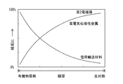
- FIG. 2 schematically shows the composition distribution in the thickness direction of the metal contained in the second electrode layer 18.
- the horizontal axis represents the film thickness of the second electrode layer 18.
- the left side of the horizontal axis is the organic layer 16 side, and the right side of the horizontal axis is the side opposite to the organic layer 16.
- the vertical axis represents the composition ratio of the highly electrically conductive metal and the charge transport material contained in the second electrode layer 18.
- the composition distribution in the film thickness direction of the metal contained in the second electrode layer 18 can be measured by ESCA analysis or the like.
- the ratio of a highly electroconductive metal is represented by molar ratio (%).
- the ratio of the highly electrically conductive metal is smaller than the ratio of the charge transport material.
- the ratio of the highly electrically conductive metal is larger than the ratio of the charge transport material.
- FIG. 2 shows an example in which the ratio of the high electrical conductivity metal is gradually increased as the distance from the organic material layer 16 increases.
- the present invention is not limited to this example. It may be inclined so that the ratio of the high electrical conductivity metal increases stepwise as the distance from the distance increases.
- the ratio of the high electrical conductivity metal is preferably 30% or less.
- the ratio of the charge transport material is relatively 70% or more, the charge injection property by the charge transport material is enhanced.
- the ratio of the highly electrically conductive metal on the organic material layer 16 side of the second electrode layer 18 is more preferably 20% or less, and further preferably 10% or less.
- the case where the ratio of a highly electroconductive metal is 0% is also included.
- the ratio of the highly electrically conductive metal is 30% or less within the range of at least 10 nm inward from the surface of the second electrode layer 18 on the organic layer 16 side.
- the charge injection property by a charge transport material can be improved more.
- the range in which the ratio of the highly electrically conductive metal is 30% or less is more preferably within 20 nm inward from the surface on the organic layer 16 side, and more preferably on the inner side from the surface on the organic layer 16 side. Within 30 nm.
- the ratio of the highly conductive metal is preferably 70% or more.
- the ratio of the charge transport material is relatively 30% or less, deterioration of the second electrode layer 18 due to oxidative deterioration of the charge transport material on the side opposite to the organic layer 16 can be suppressed.
- the ratio of the highly electrically conductive metal on the organic material layer 16 side of the second electrode layer 18 is more preferably 80% or more, and further preferably 90% or more.
- the ratio of a highly electroconductive metal is 100% is also included.
- the ratio of the highly conductive metal is 70% or more within the range of at least 10 nm inward from the surface of the second electrode layer 18 on the side opposite to the organic layer 16.
- the range in which the ratio of the highly electrically conductive metal is 70% or more is more preferably within 20 nm inward from the surface opposite to the organic material layer 16, and more preferably on the side opposite to the organic material layer 16. It is within the range within 30 nm inside from the surface.
- the ratio of the high electrical conductivity metal on the organic material layer 16 side of the second electrode layer 18 can be easily reduced. Further, it is easy to increase the ratio of the high electrical conductivity metal to nearly 100% on the opposite side of the second electrode layer 18 from the organic material layer 16. For this reason, it is particularly effective for improving the charge injection property by the charge transporting material and preventing the second electrode layer 18 from being deteriorated.
- the upper limit of the film thickness of the second electrode layer 18 is preferably 10 ⁇ m or less, more preferably 1 ⁇ m or less, and even more preferably 500 nm or less from the viewpoint of conductivity when constructed as a device.
- the lower limit of the film thickness of the second electrode layer 18 is preferably 5 nm or more, more preferably 10 nm or more, and still more preferably 50 nm or more, from the viewpoint of ensuring conductivity and ensuring uniform electron transport properties. It is good to be.
- the transparent substrate 12 of the organic semiconductor device 10 is made of a material that is transparent to visible light.
- a transparent material include a transparent ceramic material such as glass and a transparent resin material.
- Transparent resin materials include polyesters such as polyethylene terephthalate and polyethylene naphthalate, polycarbonate, polyimide, polyethersulfone, polyetherimide, polyphenylene sulfide, polysulfone, polyetheretherketone, polyamide, polymethyl methacrylate, polyarylate, and cycloolefin.
- a polymer etc. can be mentioned. These may be contained alone or in combination of two or more.
- the visible light transmittance of the transparent substrate 12 is not particularly limited, but is preferably 60% or more. More preferably, it is 70% or more.
- the thickness of the transparent substrate 12 can be appropriately determined according to the application, but there is usually no problem as long as it is within the range of 3 to 1000 ⁇ m.
- the thickness of the transparent substrate 12 is preferably 10 to 500 ⁇ m, more preferably 10 to 300 ⁇ m.
- the first electrode layer 14 is preferably formed of a material such as a metal having a high work function (for example, 4 eV or more), a conductive compound, or a mixture thereof. Typical examples of such a material include ITO (tin-doped indium oxide) and IZO (indium zinc oxide).
- the thickness of the first electrode layer 14 is usually 1 ⁇ m or less and preferably 200 nm or less.
- the resistance of the first electrode layer 14 is several hundred ⁇ / sq. The following is preferred.
- the light emitting layer is formed from an organic light emitting material, or a small amount of organic light emission on an organic material (host material) that exhibits charge transportability (hole transportability, electron transportability, or amphoteric transportability). It can form from the material which added material (dopant material).
- the light emission color can be set by selecting an organic light emitting material used for the light emitting layer.
- the thickness of the light emitting layer is preferably 200 nm or less in order to obtain practical light emission luminance.
- the light emitting layer is formed from an organic light emitting material
- a material having excellent film forming properties and excellent film stability is used as the organic light emitting material.
- organic light-emitting materials include metal complexes typified by Alq 3 (tris- (8-hydroxyquinolinato) aluminum), polyphenylene vinylene (PPV) derivatives, polyfluorene derivatives, and the like. It is done. At this time, in order to adjust the emission color, a small amount of an organic light-emitting material which is difficult to form a stable thin film by itself such as a fluorescent dye can be added. Examples of fluorescent dyes include coumarin, DCM derivatives, quinacridone, perylene, and rubrene.
- the organic light emitting material described above can be used as the organic light emitting material.
- the organic light emitting material since the amount of the organic light emitting material in the light emitting layer is relatively small, it is preferable to use a fluorescent dye or the like.
- the fluorescent dye described above can be used as the fluorescent dye.
- the host material include Alq 3 , TPD (triphenyldiamine), an electron transporting oxadiazole derivative (PBD), a polycarbonate copolymer, and polyvinyl carbazole.
- Examples of the material for forming the hole transport layer include tetraarylbenzidine compounds, triphenylene derivatives, water-soluble PEDOT: PSS (polystyrene sulfonic acid-doped polyethylene dioxythiophene), and the like.
- the thickness of the hole transport layer is preferably 20 to 100 nm.
- an electron accepting acceptor is preferably added to the hole transport layer.
- electron accepting acceptors include metal halides, Lewis acids, organic acids and the like.
- the hole transport layer can be formed by diluting in an alcohol solvent such as isopropyl alcohol, applying by spin coating, etc., heating and drying.
- the upper limit of the thickness of the organic layer 16 is preferably 1 ⁇ m or less, more preferably 500 nm or less, and even more preferably 300 nm or less from the viewpoint of obtaining practical light emission luminance.
- the lower limit of the thickness of the organic material layer 16 is preferably 1 nm or more, more preferably 5 nm or more, and further preferably 10 nm or more from the viewpoint of obtaining practical light emission luminance.
- the material for forming the photoelectric conversion layer is not particularly limited as long as it is a material having an electron donating property or an electron accepting property.
- conductive polymers such as organic single crystals such as pentacene, poly-3-methylthiophene, polyacetylene, polyphenylene and derivatives thereof, polyphenylene vinylene and derivatives thereof, polysilane and derivatives thereof, polyalkylthiophene and derivatives thereof, and the like Derivatives thereof, porphyrin derivatives, phthalocyanine derivatives, merocyanine derivatives, synthetic pigments such as chlorophyll, organometallic polymers, and the like can be mentioned.
- the organic materials having electron accepting properties include CN-poly (phenylene-vinylene), MEH-CN-PPV, -CN group or -CF 3 group-containing polymers, and -CF 3 Examples thereof include substituted polymers, poly (fluorene) derivatives, fullerene derivatives such as C60, carbon nanotubes, perylene derivatives, polycyclic quinones, and quinacridones.
- examples of the organic material having an electron-donating property include materials such as polyphenylene and derivatives thereof, polyphenylene vinylene and derivatives thereof, polysilane and derivatives thereof, polyalkylthiophene and derivatives thereof, porphyrin derivatives, phthalocyanine derivatives, and organometallic polymers. Can do.
- the upper limit of the thickness of the organic material layer 16 (photoelectric conversion layer) is preferably 1 ⁇ m or less, more preferably 500 nm or less, and still more preferably from the viewpoint of obtaining practical power generation characteristics. It is good that it is 200 nm or less.
- the lower limit of the thickness of the organic material layer 16 (photoelectric conversion layer) is preferably 1 nm or more, more preferably 5 nm or more, and further preferably 10 nm or more from the viewpoint of obtaining practical power generation characteristics. good.
- a protective layer can be further formed on the second electrode layer 18.
- the protective layer may be in the form of a film such as a hard coat or a vapor-deposited film, or in the form of a film formed by bonding or the like.
- the material for the protective layer may be any material having an insulating property, and may be transparent to visible light or may not be transparent to visible light. Specific examples include metals such as SUS, ceramics such as glass, and resins. Further, a laminate of these metals, ceramics, and resins may be used. Examples of the resin include the same ones listed in the transparent substrate 12. Moreover, an acrylic material, a silicone material, etc. suitable as a hard coat can be mentioned.
- the thickness of the protective layer is usually 3 to 1000 ⁇ m, preferably 10 to 500 ⁇ m, more preferably 10 to 300 ⁇ m.
- the first electrode layer 14 is formed on the transparent substrate 12
- the organic layer 16 is formed on the first electrode layer 14
- the first layer is formed on the organic layer 16. It can be manufactured by forming the two-electrode layer 18 and forming a protective layer on the second electrode layer 18 as necessary.
- the first electrode layer 14 can be formed by a vacuum deposition method, a sputtering method, a spin coating method, a casting method, an LB method, a pyrosol method, a spray method, or the like.
- the light emitting layer of the organic EL element in the organic material layer 16 can be formed by diluting an organic light emitting material or the like in an organic solvent, applying it by spin coating, etc., heating and drying.
- the photoelectric conversion layer of the organic thin-film solar cell in the organic material layer 16 can be formed by diluting the material forming the photoelectric conversion layer in an organic solvent, applying it by spin coating, etc., heating and drying.
- the hole transport layer of the organic material layer 16 can be formed by vacuum deposition, spin coating, casting, LB, printing, or the like.
- the protective layer may be formed directly on the second electrode layer 18 or may be formed on the second electrode layer 18 with an adhesive layer made of an adhesive or the like interposed therebetween.
- the film-like protective layer can be formed using a method such as a vacuum deposition method, a spin coating method, a casting method, an LB method, or a printing method.
- the film-like protective layer may be, for example, a method in which a film material is placed directly on the second electrode layer 18, and a part of the film material is melted and bonded to the second electrode layer 18. It can be formed using a method such as a method of laminating a film material by placing an adhesive layer made of an adhesive or the like on the two-electrode layer 18.
- the second electrode layer 18 can be formed by co-evaporation of a highly electrically conductive metal and a charge transport material. At this time, the ratio between the high electrical conductivity metal and the charge transport material is changed over time while taking into consideration the adhesion probability between the metals, and the ratio of the high electrical conductivity metal becomes the organic layer of the second electrode layer 18. As the distance from the organic material layer 16 increases, the ratio of the highly conductive metal decreases so as to be smaller than the ratio of the charge transport material on the side 16 and larger than the ratio of the charge transport material on the side opposite to the organic layer 16 of the second electrode layer 18. Try to increase the ratio.
- the initial film formation rate of the high electrical conductivity metal is lowered to near zero. More specifically, it is preferable to set the initial film formation rate of the highly conductive metal to 0.005 ⁇ / s or less. More preferably, it is 0.003 liter / s or less, More preferably, it is 0.001 liter / s or less. In addition, it is preferable to set the initial film formation rate ratio of the high electrical conductivity metal to the charge transport material (high electrical conductivity metal / charge transport material) to 1/500 or less while considering the adhesion probability between the metals. The initial film formation rate ratio is more preferably 1/750 or less, and still more preferably 1/1000 or less.
- the final film formation rate of the high electrical conductivity metal is increased. More specifically, it is preferable to set the final film formation rate of the high electrical conductivity metal to 0.500 ⁇ / s or more. More preferably, it is 1.000 kg / s or more, and further preferably 2.000 kg / s or more. In addition, it is preferable to set the final film formation rate ratio of the high electrical conductivity metal to the charge transport material (high electrical conductivity metal / charge transport material) to 500/1 or more in consideration of the probability of adhesion between metals. The film formation rate ratio at the end is more preferably 750/1 or more, and further preferably 1000/1 or more.
- the deposition rate of the high electrical conductivity metal is increased with time.
- the film formation rate of the highly electrically conductive metal may be gradually increased over time, or may be increased stepwise.
- the film formation rate program is preferably a program that approximates the following equation.
- y 1 [(r e ⁇ r s ) / t] + r s
- y 2 [(R e ⁇ R s ) / t] + R s
- y 1 Film formation rate of highly conductive metal
- y 2 Film formation rate of charge transport material
- the composition distribution as shown in FIG. 3 is obtained.
- the ratio of the highly electrically conductive metal is substantially the same as the ratio of the charge transport material (1: 1) on the organic layer 16 side of the second electrode layer 18.
- the ratio of the highly electrically conductive metal is smaller than the ratio of the charge transport material.
- the ratio of the high electrical conductivity metal decreases as the distance from the organic layer 16 increases.
- the ratio of the charge transport material increases as the distance from the organic material layer 16 increases.
- the second electrode is configured such that the ratio of the highly electrically conductive metal is larger than the ratio of the charge transport material, and as a whole, the ratio of the highly electrically conductive metal increases as the distance from the organic material layer 16 increases.
- the metal composition of layer 18 cannot be graded.
- Example 1 A polyethylene naphthalate (PEN) film having a thickness of 200 ⁇ m used as a transparent substrate was heat-dried under vacuum in a vacuum oven to remove adhering water and contained water in advance. On the surface of this transparent substrate, an indium tin oxide (ITO) layer having a thickness of 150 nm was formed as a positive electrode layer. This was subjected to ultrasonic cleaning for 5 minutes each in the order of pure water, an organic alkali cleaning solution (manufactured by Melfu: EFTRAN), pure water, an acetone solution, and an IPA solution, and then treated with a UV ozone cleaner for 10 minutes.
- ITO indium tin oxide
- a coating liquid for forming a hole transport layer [PEDOT: PSS aqueous solution (manufactured by Heraeus) diluted with ethanol] is formed on the cleaned ITO layer surface by spin coating, and then heated on a 130 ° C. hot plate. It dried for 30 minutes and formed the 60-nm-thick hole transport layer.
- a polyfluorene-based light emitting material (glass transition temperature: 116 ° C., DSC method) as a light emitting layer material is applied to the surface of the hole transport layer by a spin coat method so as to have a thickness of 80 nm, and dried to form a light emitting layer. Formed.
- the light emitting layer was formed in a glove box in a nitrogen atmosphere having an oxygen concentration of 0.01 ppm and a water concentration of -88 ° C. at a dew point.
- the negative electrode layer was formed in the glove box following the formation of the light emitting layer.
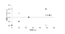
- FIG. 4 shows the relationship between the film formation rate and the elapsed time.
- the organic EL device according to the example has an ITO layer (150 nm) as a positive electrode layer, a hole transport layer (60 nm), a light emitting layer (80 nm), and an Al as a negative electrode layer on a PEN film (film thickness 200 ⁇ m). -Ca layer (200 nm) is formed in order.
- an electron injection layer having a film thickness of 35 nm is formed on the surface of the light emitting layer by vacuum evaporation, and a 35 nm-thickness electron injection layer is formed on the surface of the electron injection layer.
- a negative electrode layer having a film thickness of 165 nm was formed by evaporating Al.
- the film formation rate was set to 2.0 ⁇ / s. Except this, it carried out similarly to the Example, and obtained the organic EL element which concerns on a comparative example.
- the metal composition distribution in the negative electrode layer of the organic EL device according to the produced example was measured by ESCA analysis.
- the apparatus used for the analysis is ESCA5600 (manufactured by ULVAC-PHI).
- the measurement conditions were as follows: X-Ray: Mg conventional 300 W ⁇ 14 kV, photoelectron extraction angle: 45 °, analysis area: 800 ⁇ m, neutralizing gun: used.
- ion etching etching gas: Ar, beam pressure: 3 kV, etching interval: 2 min
- FIG. 5 shows the relationship between the etching depth direction (nm) and the Al / Ca ratio (molar ratio (%)).
- the Al ratio is smaller than the Ca ratio.
- the Al ratio is larger than the Ca ratio.
- the ratio of Ca is decreasing as it leaves
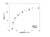
- FIG. 6 shows the relationship between the current density and the luminance of the organic EL elements according to Examples and Comparative Examples.
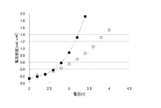
- FIG. 7 shows the relationship between the voltage and current density of the organic EL elements according to Examples and Comparative Examples.
- the organic EL element of the comparative example is one in which an electron injection layer for improving the light emission characteristics is formed as a layer different from the negative electrode layer.
- the organic EL element of the example is one in which an electron injecting Ca for improving the light emission characteristics is contained together with Al in a single negative electrode layer.
- any organic EL element contains Ca of charge injection property, it has excellent luminous efficiency (the organic EL element of the example has excellent luminous characteristics equivalent to the organic EL element of the comparative example). Show.)
- the organic EL element of the example can lower the driving voltage required to obtain the same luminance (the same current density). It could be confirmed. This is because, in the comparative example, a contact resistance is generated between the electron injection layer and the negative electrode layer, and the driving voltage is increased, whereas in the example, the contact resistance is not generated as in the comparative example. This is presumably because the rise in voltage was suppressed.
- the negative electrode layer of the example has a high electroconductive metal ratio of 30% within the range of 30 nm inward from the surface on the organic layer side (etching depth direction is 0 nm). It turns out that it is the following. Further, it can be seen that the ratio of the highly electrically conductive metal is 70% or more within the range of 30 nm or less inward from the surface opposite to the organic layer (etching depth direction is 200 nm).
- the present invention is not limited to the above-described embodiments and examples, and various modifications can be made without departing from the spirit of the present invention.
- the present invention is applied to an organic EL element has been described.
- an improvement in power generation characteristics can be expected.
Landscapes
- Physics & Mathematics (AREA)
- Optics & Photonics (AREA)
- Electroluminescent Light Sources (AREA)
- Photovoltaic Devices (AREA)
Abstract
接触抵抗による不具合を抑えつつ、性能改善を図ることが可能な有機半導体デバイスを提供する。 有機半導体デバイス10の第2電極層18は、体積抵抗率が3.0×10⁻⁶Ω・cm以下の高電気伝導性金属と、アルカリ土類金属、アルカリ金属、アルカリ土類金属のハロゲン化物、アルカリ金属のハロゲン化物、Co酸化物、Cu酸化物、Mo酸化物、Ni酸化物、アミン系有機化合物、ヒドラゾン系有機化合物、スチルベン系有機化合物、スターバスト系有機化合物、フタロシアニン系有機化合物よりなる群から選択される1以上の電荷輸送材料と、の共蒸着により有機物層16の他方面に直接形成されたものであり、第2電極層18における高電気伝導性金属の比率が、第2電極層18の有機物層16側では電荷輸送材料の比率よりも小さくなり、第2電極層18の有機物層16と反対側では電荷輸送材料の比率よりも大きくなるように、有機物層16から離れるに従い上昇するようにした。
Description
本発明は、有機半導体デバイスおよび電極膜に関し、さらに詳しくは、有機エレクトロルミネッセンス素子(有機EL素子)や有機薄膜太陽電池などに好適な有機半導体デバイスおよび電極膜に関するものである。
従来、半導体デバイスに有機物を用いた有機半導体デバイスが知られている。例えば、この種の有機半導体デバイスとして、発光材料として有機物材料を用いた有機エレクトロルミネッセンス素子(有機EL素子)や、導電性ポリマーやフラーレン等を組み合わせた有機物材料を用いた有機薄膜太陽電池などがある。
例えば、特許文献1には、透明基板の表面に、陽電極層(ITO層等)と、発光層を含む有機物層とが積層された陽電極基板と、樹脂フィルムの表面に、陰電極層(Mg-Ag合金等)が積層された陰電極フィルムとを、互いに重ね合わせて加熱・加圧して貼り合わせた有機EL素子が開示されている。同文献には、陰電極層の有機物層側に電子注入層(LiF等のアルカリ金属化合物等)を付設すると、発光特性を改良できる点が記載されている。
また、特許文献2は、絶縁性基板上に、陽極、正孔注入層、発光層、陰極層、酸化物絶縁層とを順次積層して形成した有機EL素子が開示されている。そして、陰極層を、例えば、Caが存在するAl層(発光層側)と、Caが存在しないAl層(発光層と反対側)との2層構造から構成した点が記載されている。
しかしながら、上記する従来の有機EL素子においては、発光特性を改良するための電子注入層を陰電極層とは別の層として形成している。このため、電子注入層と陰電極層との間に界面が形成されることとなり、電子注入層と陰電極層との間で接触抵抗が生じる。有機EL素子は電流駆動であるため、接触抵抗によって駆動電圧が高くなるという問題が生じる。
このことは、例えば有機薄膜太陽電池でも同様である。すなわち、有機薄膜太陽電池は、光電変換材料としての導電性有機ポリマーなどを含む有機物層(光電変換層)の一方面に陽電極層を備え、他方面に陰電極層を備えるが、陰電極層の有機物層側にアルカリ金属等からなるバッファ層を付設する場合がある。
しかしながら、有機薄膜太陽電池において、バッファ層と陰電極層とを別々の層として形成すると、バッファ層と陰電極層との間に界面が形成され、バッファ層と陰電極層との間で接触抵抗が生じる。有機薄膜太陽電池は電流駆動であるため、接触抵抗によって発電量あるいは取り出し電流効率が低下するという問題が生じる。
そこで、本発明が解決しようとする課題は、接触抵抗による不具合を抑えつつ、性能改善を図ることが可能な有機半導体デバイスおよび電極膜を提供することにある。
上記課題を解決するため、本発明に係る有機半導体デバイスは、有機半導体の有機物層の一方面に第1電極層を備えるとともに他方面に第2電極層を備え、前記第2電極層は、体積抵抗率が3.0×10⁻⁶Ω・cm以下の高電気伝導性金属と、アルカリ土類金属、アルカリ金属、アルカリ土類金属のハロゲン化物、アルカリ金属のハロゲン化物、Co酸化物、Cu酸化物、Mo酸化物、Ni酸化物、アミン系有機化合物、ヒドラゾン系有機化合物、スチルベン系有機化合物、スターバスト系有機化合物、および、フタロシアニン系有機化合物よりなる群から選択される1以上の電荷輸送材料と、の共蒸着により前記有機物層の他方面に直接形成されたものであり、前記第2電極層における高電気伝導性金属の比率が、前記第2電極層の有機物層側では前記電荷輸送材料の比率よりも小さくなり、前記第2電極層の有機物層と反対側では前記電荷輸送材料の比率よりも大きくなるように、前記有機物層から離れるに従い上昇していることを要旨とするものである。
ここで、前記第2電極層の有機物層側での高電気伝導性金属の比率は30%以下であり、前記第2電極層の有機物層と反対側での高電気伝導性金属の比率は70%以上であることが好ましい。この際、前記第2電極層の有機物層側表面から内側に少なくとも10nm以内の範囲内では、前記高電気伝導性金属の比率が30%以下であることが望ましい。また、前記第2電極層の有機物層と反対側表面から内側に少なくとも10nm以内の範囲内では、前記高電気伝導性金属の比率が70%以上であることが望ましい。
そして、前記高電気伝導性金属は、Al、Ag、Au、および、Cuから選択される1種または2種以上の金属であることが好ましい。さらに、前記第2電極層は、AlとCaとの共蒸着、あるいは、AgとMgとの共蒸着により、前記有機物層の他方面に直接形成されたものであることが好ましい。
一方、本発明に係る電極膜は、有機半導体デバイスの電極層に用いられる電極膜であって、体積抵抗率が3.0×10⁻⁶Ω・cm以下の高電気伝導性金属と、アルカリ土類金属、アルカリ金属、アルカリ土類金属のハロゲン化物、アルカリ金属のハロゲン化物、Co酸化物、Cu酸化物、Mo酸化物、Ni酸化物、アミン系有機化合物、ヒドラゾン系有機化合物、スチルベン系有機化合物、スターバスト系有機化合物、および、フタロシアニン系有機化合物よりなる群から選択される1以上の電荷輸送材料と、の共蒸着により形成され、前記高電気伝導性金属の比率が、一方面側では前記電荷輸送材料の比率よりも小さくなり、他方面側では前記電荷輸送材料の比率よりも大きくなるように、一方面側から他方面側に向かって上昇していることを要旨とするものである。
本発明に係る有機半導体デバイスによれば、高電気伝導性金属と電荷輸送材料との共蒸着で有機物層の他方面に第2電極層が直接形成されているため、接触抵抗による不具合を抑えつつ、性能改善を図ることができる。このとき、第2電極層の有機物層側で高電気伝導性金属の比率を電荷輸送材料の比率よりも小さくしているため、電荷輸送材料による電子注入性の向上を図ることができる。また、第2電極層の有機物層と反対側で高電気伝導性金属の比率を電荷輸送材料の比率よりも大きくしているため、電荷輸送材料の酸化劣化が抑えられ、第2電極層の劣化防止を図ることができる。
したがって、本発明に係る有機半導体デバイスを、例えば、有機EL素子に適用した場合には、従来に比べ、発光効率の向上を図ることができる。また例えば、有機薄膜太陽電池に適用した場合には、従来に比べ、発電特性の向上が期待できる。
ここで、第2電極層の有機物層側での高電気伝導性金属の比率が30%以下であると、電荷輸送材料による電荷注入性の向上効果に優れる。また、第2電極層の有機物層と反対側での高電気伝導性金属の比率が70%以上であると、電荷輸送材料の酸化劣化による第2電極層の劣化が抑えられる効果に優れる。
そして、AlとCaとの共蒸着、あるいは、AgとMgとの共蒸着により第2電極層が形成される場合には、接触抵抗による不具合を抑えつつ性能改善を図る効果が高い。特に、AlとCaとの共蒸着による場合には、第2電極層の有機物層側で高電気伝導性金属の比率を極めて小さくできるとともに、第2電極層の有機物層と反対側で高電気伝導性金属の比率を100%近くまで上げることができるため、電荷輸送材料による電荷注入性の向上と第2電極層の劣化防止に対して特に効果的である。また、Alを有機EL素子の陰極金属として構成し、Caを有機EL素子の電子注入材料として機能させることで、発光特性に優れた有機EL素子を得ることができる。
そして、本発明に係る電極膜によれば、高電気伝導性金属と電荷輸送材料との共蒸着により形成され、高電気伝導性金属の比率が、一方面側では電荷輸送材料の比率よりも小さくなり、他方面側では電荷輸送材料の比率よりも大きくなるように、一方面側から他方面側に向かって上昇していることから、有機半導体デバイスの電極層に用いたときには、接触抵抗による不具合を抑えつつ、有機半導体デバイスの性能改善を図ることができる。このとき、一方面側では、電荷輸送材料による電荷注入性の向上を図ることができる。また、他方面側では、電荷輸送材料の酸化劣化が抑えられるため、有機半導体デバイスの電極層の劣化防止を図ることができる。
以下に、本発明に係る有機半導体デバイスおよび電極膜について詳細に説明する。
図1は、本発明の一実施形態に係る有機半導体デバイスの断面を示した模式図である。図1に示すように、有機半導体デバイス10は、フィルム状あるいは板状に形成された透明材料よりなる透明基材12と、透明基材12の上に形成された第1電極層14と、第1電極層14の上に形成された有機物層16と、有機物層16の上に形成された第2電極層18と、を備えている。有機物層16は、有機半導体デバイス10の機能を発揮させる部位であり、その種類に応じた材料が用いられる。
有機半導体デバイス10は、例えば、有機EL素子、有機薄膜太陽電池などとして好適に用いることができる。この場合、製造上の理由などから、透明基材12の上に形成された第1電極層14を陽極層とし、有機物層16の上に形成された第2電極層18を陰極層とすることが好ましい。
有機EL素子の場合、有機物層16には有機発光材料が含まれる。有機物層16には、有機発光材料に加えて、電荷輸送性(正孔輸送性、電子輸送性、両性輸送性)を有する有機材料(ホスト材料)が含まれていても良い。有機EL素子における有機物層16は、これらの材料を単一層に含む単一層で構成されていても良いし、有機発光材料を含む層やホスト材料を含む層などの層を含む複数層で構成されていても良い。
有機EL素子において、有機物層16が複数層で構成される場合としては、有機発光材料を含む発光層の第1電極層14側に正孔輸送性を有する有機材料を含む正孔輸送層を備える構成や、有機発光材料を含む発光層の第2電極層18側に電子輸送性を有する有機材料を含む電子輸送層を備える構成や、これらの両方を備える構成などを挙げることができる。なお、有機物層16が複数層で構成される場合であっても、有機発光材料を含む発光層中に電荷輸送性を有する有機材料(ホスト材料)がさらに含まれていても良い。
有機薄膜太陽電池の場合、有機物層16(光電変換層)には、電子供与性を有する有機材料(p型有機半導体材料)や電子受容性を有する有機材料(n型有機半導体材料)が含まれる。有機薄膜太陽電池には、ショットキー型の有機薄膜太陽電池や、ヘテロ接合型の有機薄膜太陽電池がある。また、ヘテロ接合型の有機薄膜太陽電池には、バイレイヤー型のものとバルクヘテロ型のものがある。
ショットキー型の有機薄膜太陽電池の場合、有機物層16には、電子供与性を有する有機材料または電子受容性を有する有機材料が含まれる。
バイレイヤー型の有機薄膜太陽電池の場合、有機物層16として、電子受容性を有する有機材料が含まれる電子輸送層と、電子供与性を有する有機材料が含まれる正孔輸送層とを別個に形成し、これらの界面において形成されるpn接合を利用して光電荷分離を生じさせ、光電流を得る。この場合、電子輸送層と正孔輸送層との間に、異なる波長の光をそれぞれ効率よく光電流に変換するための光捕集層を設けても良い。
バルクヘテロ型の有機薄膜太陽電池の場合、有機物層16として、電子受容性を有する有機材料と電子供与性を有する有機材料とが含まれる電子正孔輸送層を形成する。電子正孔輸送層内でバルクの状態で存在するp型有機半導体材料とn型有機半導体材料によるpn接合を利用して光電荷分離を生じさせ、光電流を得る。
第2電極層18は、このような構成の有機物層16の上に、電極材料となる高電気伝導性金属と高電気伝導性金属に添加される電荷輸送材料との共蒸着により直接形成される。なお、第2電極層18は、これらの高電気伝導性金属、電荷輸送材料以外に、製造上、不可避な不純物を含んでいても良い。
第2電極層18は、高電気伝導性金属と電荷輸送材料との共蒸着により直接形成されており、高電気伝導性金属と電荷輸送材料とが第2電極層18の単一層内でそれぞれバルクの状態で存在するバルクヘテロ構造であるため、高電気伝導性金属と電荷輸送材料との接触において接触抵抗が生じることはない。従来、例えば有機EL素子においては、発光特性を改良するための電子注入層を陰電極層とは別の層として形成していたが、電子注入層と陰電極層との間で接触抵抗が生じることが問題であった。本発明においては、高電気伝導性金属よりなる層と電荷輸送材料よりなる層とを別々の層として形成するものではないため、このような接触抵抗が生じるのを抑えることができる。
高電気伝導性金属は、体積抵抗率が3.0×10⁻⁶Ω・cm以下の金属である。具体的には、Al、Ag、Au、Cuなどを挙げることができる。これらは単独で用いても良いし、2以上を組み合わせて用いても良い。これらのうちでは、電荷輸送材料との相性等の観点から、Al、Agが好ましい。
電荷輸送材料は、第2電極層18の性能改善のため、電荷注入性(電子注入性あるいは正孔注入性)を向上させるなどの目的で添加される。
電子注入性を向上させる材料としては、アルカリ土類金属、アルカリ金属、アルカリ土類金属のハロゲン化物、アルカリ金属のハロゲン化物、フタロシアニン系有機化合物(有機化合物には有機金属錯体も含まれる。)を挙げることができる。電子注入材料として好適なアルカリ土類金属としては、Mg、Ca、Sr、Baなどを挙げることができる。電子注入材料として好適なアルカリ金属としては、Li、Na、K、Rb、Csなどを挙げることができる。電子注入材料として好適なアルカリ土類金属のハロゲン化物としては、アルカリ土類金属のフッ化物、特に、フッ化カルシウム、フッ化マグネシウムなどを挙げることができる。電子注入材料として好適なアルカリ金属のハロゲン化物としては、アルカリ金属のフッ化物、特に、フッ化ナトリウム、フッ化カリウム、フッ化リチウムなどを挙げることができる。電子注入材料として好適なフタロシアニン系有機化合物としては、フッ素化フタロシアニン、中心金属としてCuやZnなどの金属を有するフッ素化フタロシアニンなどを挙げることができる。これらは単独で用いても良いし、2以上を組み合わせて用いても良い。これらのうちでは、取り扱い性に優れるなどの観点から、Mg、Ca、Sr、Baが好ましい。有機EL素子の場合には、Mg、Ca、Sr、Baを電子注入材料として機能させることで、優れた有機EL素子を得ることができる。また、化学的に安定で、長寿命化に効果があるなどの観点から、アルカリ金属のフッ化物、アルカリ土類金属のフッ化物、特に、フッ化ナトリウム、フッ化リチウムが好ましい。有機EL素子の場合には、アルカリ金属のフッ化物、アルカリ土類金属のフッ化物、特に、フッ化ナトリウム、フッ化リチウムを電子注入材料として機能させることで、優れた有機EL素子を得ることができる。
正孔注入性を向上させる材料としては、Co酸化物、Cu酸化物、Mo酸化物、Ni酸化物、アミン系有機化合物、ヒドラゾン系有機化合物、スチルベン系有機化合物、スターバスト系有機化合物(これらの有機化合物には有機金属錯体も含まれる。)を挙げることができる。正孔注入材料として好適な金属酸化物としては、Co3O4、CuO、MoOx(xは整数)、NiOx(xは整数)などを挙げることができる。正孔注入材料として好適な有機化合物としては、4,4’-ビス[N-ナフチル-N-フェニル-アミノ]ビフェニル(α-NPD)、銅フタロシアニン(CuPc)などを挙げることができる。これらは単独で用いても良いし、2以上を組み合わせて用いても良い。
高電気伝導性金属と電荷輸送材料の組み合わせのうち、相性等の理由から好ましい組み合わせとしては、Al-Ca、Al-Sr、Al-Ba、Ag-Mgを挙げることができる。より好ましい組み合わせはAl-Ca、Ag-Mgであり、特に好ましい組み合わせはAl-Caである。Alを有機EL素子の陰極材料とし、Caを有機EL素子の電子注入材料として機能させることで、発光特性に優れた有機EL素子を得ることができる。また、長寿命化の観点では、Al-フッ化ナトリウム(NaF)、Al-フッ化リチウム(LiF)が好ましい組み合わせである。Alを有機EL素子の陰極材料にし、フッ化ナトリウムまたはフッ化リチウムを有機EL素子の電子注入材料として機能させることで、発光特性と長寿命化を両立する、バランスのとれた有機EL素子を得ることができる。
そして、第2電極層18は、高電気伝導性金属の比率が厚み方向に沿って傾斜するように形成されている。図2は、第2電極層18に含まれる金属の厚み方向の組成分布を模式的に示したものである。図2において、横軸は、第2電極層18の膜厚である。横軸の左側は有機物層16側であり、横軸の右側は有機物層16と反対側である。縦軸は、第2電極層18に含まれる高電気伝導性金属と電荷輸送材料の組成比である。第2電極層18に含まれる金属の膜厚方向の組成分布は、ESCA分析などにより測定することができる。なお、高電気伝導性金属の比率は、モル比(%)で表される。
図2に示すように、第2電極層18の有機物層16側では、高電気伝導性金属の比率が電荷輸送材料の比率よりも小さくなっている。また、第2電極層18の有機物層16と反対側では、高電気伝導性金属の比率が電荷輸送材料の比率よりも大きくなっている。そして、全体として、高電気伝導性金属の比率は、有機物層16から離れるに従い上昇している。また、電荷輸送材料の比率は、有機物層16から離れるに従い減少している。
図2では、有機物層16から離れるに従い、高電気伝導性金属の比率が漸次大きくなるように傾斜している例を示しているが、本発明においては、これに限定されず、例えば有機物層16から離れるに従い、高電気伝導性金属の比率が段階的に大きくなるように傾斜していても良い。
第2電極層18の有機物層16側においては、高電気伝導性金属の比率は30%以下であることが好ましい。この場合、相対的に、電荷輸送材料の比率が70%以上となるため、電荷輸送材料による電荷注入性が高まる。この観点から、第2電極層18の有機物層16側における高電気伝導性金属の比率は、より好ましくは20%以下、さらに好ましくは10%以下である。なお、第2電極層18の有機物層16側においては、高電気伝導性金属の比率が0%である場合も含まれる。
このとき、第2電極層18の有機物層16側の表面から内側に少なくとも10nm以内の範囲内では、高電気伝導性金属の比率は30%以下であることが好ましい。これにより、電荷輸送材料による電荷注入性をより高めることができる。この観点から、高電気伝導性金属の比率が30%以下である範囲としては、より好ましくは有機物層16側の表面から内側に20nm以内の範囲内、さらに好ましくは有機物層16側の表面から内側に30nm以内の範囲内である。
第2電極層18の有機物層16と反対側においては、高電気伝導性金属の比率は70%以上であることが好ましい。この場合、相対的に、電荷輸送材料の比率が30%以下となるため、有機物層16と反対側での電荷輸送材料の酸化劣化による第2電極層18の劣化を抑えることができる。この観点から、第2電極層18の有機物層16側における高電気伝導性金属の比率は、より好ましくは80%以上、さらに好ましくは90%以上である。なお、第2電極層18の有機物層16側と反対側においては、高電気伝導性金属の比率が100%である場合も含まれる。
このとき、第2電極層18の有機物層16と反対側の表面から内側に少なくとも10nm以内の範囲内では、高電気伝導性金属の比率は70%以上であることが好ましい。これにより、有機物層16と反対側での電荷輸送材料の酸化劣化による第2電極層18の劣化を抑える効果をより高めることができる。この観点から、高電気伝導性金属の比率が70%以上である範囲としては、より好ましくは有機物層16と反対側の表面から内側に20nm以内の範囲内、さらに好ましくは有機物層16と反対側の表面から内側に30nm以内の範囲内である。
第2電極層18が、AlとCaとの共蒸着による場合には、第2電極層18の有機物層16側で高電気伝導性金属の比率を極めて小さくしやすい。また、第2電極層18の有機物層16と反対側で高電気伝導性金属の比率を100%近くまで上げやすい。このため、電荷輸送材料による電荷注入性の向上と第2電極層18の劣化防止に対して特に効果的である。
第2電極層18の膜厚の上限は、デバイスとして構築した際の導電性などの観点から、好ましくは、10μm以下、より好ましくは、1μm以下、さらに好ましくは、500nm以下であると良い。一方、第2電極層18の膜厚の下限は、導電性の確保、均一な電子輸送性の確保などの観点から、好ましくは、5nm以上、より好ましくは、10nm以上、さらに好ましくは、50nm以上であると良い。
有機半導体デバイス10の透明基材12は、可視光に対して透明な材料により形成されている。このような透明材料としては、ガラスなどの透明セラミック材料や、透明樹脂材料などを挙げることができる。透明樹脂材料としては、ポリエチレンテレフタレート、ポリエチレンナフタレート等のポリエステル、ポリカーボネート、ポリイミド、ポリエーテルスルフォン、ポリエーテルイミド、ポリフェニレンサルファイド、ポリスルホン、ポリエーテルエーテルケトン、ポリアミド、ポリメタクリル酸メチル、ポリアリレート、シクロオレフィンポリマーなどを挙げることができる。これらは1種または2種以上含まれていても良い。
透明基材12の可視光透過率としては、特に限定されるものではないが、60%以上であることが好ましい。より好ましくは70%以上である。透明基材12の厚みは、用途に応じて適宜定めることができるが、通常、3~1000μmの範囲内であれば問題ない。透明基材12の厚みとしては、好ましくは10~500μm、より好ましくは10~300μmである。
第1電極層14は、仕事関数の大きい(例えば4eV以上の)金属、導電性化合物、または、これらの混合物などの材料により形成されることが好ましい。このような材料としては、ITO(錫ドープ酸化インジウム)、IZO(インジウム亜鉛酸化物)などを代表的なものとして挙げることができる。第1電極層14の厚みは、通常、1μm以下であり、200nm以下が好ましい。第1電極層14の抵抗は、数百Ω/sq.以下が好ましい。
有機EL素子においては、発光層は、有機発光材料から形成するか、電荷輸送性(正孔輸送性、電子輸送性、または、両性輸送性)を示す有機材料(ホスト材料)に少量の有機発光材料(ドーパント材料)を添加した材料より形成することができる。発光層に用いる有機発光材料の選択により、発光色を設定することができる。発光層の厚みは、実用的な発光輝度を得るために、200nm以下が好ましい。
発光層を有機発光材料から形成する場合、有機発光材料としては、成膜性に優れ、膜の安定性に優れた材料が用いられる。このような有機発光材料としては、具体的には、例えば、Alq3(トリス-(8-ヒドロキシキノリナト)アルミニウム)に代表される金属錯体、ポリフェニレンビニレン(PPV)誘導体、ポリフルオレン誘導体などが挙げられる。この際、発光色を調節するために、蛍光色素などの単独では安定な薄膜を形成し難い有機発光材料を少量添加することもできる。蛍光色素としては、クマリン、DCM誘導体、キナクリドン、ペリレン、ルブレンなどを挙げることができる。
発光層をホスト材料とともに有機発光材料で形成する場合にも、有機発光材料としては、上述する有機発光材料を用いることができる。この場合、発光層における有機発光材料の量が相対的に少なくなることから、蛍光色素などを用いること好ましい。蛍光色素には、上述する蛍光色素を用いることができる。ホスト材料としては、上記Alq3 、TPD(トリフェニルジアミン)、電子輸送性のオキサジアゾール誘導体(PBD)、ポリカーボネート系共重合体、ポリビニルカルバゾールなどを挙げることができる。
正孔輸送層を形成する材料としては、テトラアリールベンジシン化合物、トリフェニレン誘導体、水溶性のPEDOT:PSS(ポリスチレンスルフォン酸ドープポリエチレンジオキシチオフェン)などを例示することができる。正孔輸送層の厚みは、20~100nmが好ましい。
正孔輸送層には、その正孔移動度を改善するために、電子受容性アクセプタを添加することが好ましい。電子受容性アクセプタの例としては、ハロゲン化金属、ルイス酸、有機酸などが挙げられる。正孔輸送層にPEDOT:PSSを用いる場合は、イソプロピルアルコールなどのアルコール系溶媒に希釈し、スピンコート等で塗工し、加熱して乾燥することで形成することができる。
有機EL素子においては、有機物層16の厚みの上限は、実用的な発光輝度を得るなどの観点から、好ましくは、1μm以下、より好ましくは、500nm以下、さらに好ましくは、300nm以下であると良い。一方、有機物層16の厚みの下限は、実用的な発光輝度を得るなどの観点から、好ましくは、1nm以上、より好ましくは、5nm以上、さらに好ましくは、10nm以上であると良い。
ショットキー型有機薄膜太陽電池においては、光電変換層を形成する材料は、電子供与性または電子受容性の性質を有する材料であれば特に限定されない。具体的には、ペンタセンなどの有機単結晶、ポリ-3-メチルチオフェン、ポリアセチレン、ポリフェニレンおよびその誘導体、ポリフェニレンビニレンおよびその誘導体、ポリシランおよびその誘導体、ポリアルキルチオフェンおよびその誘導体等の導電性高分子およびその誘導体、ポルフィリン誘導体、フタロシアニン誘導体、メロシアニン誘導体、クロロフィル等の合成色素、有機金属ポリマー等を挙げることができる。
ヘテロ接合型有機薄膜太陽電池において、電子受容性を有する有機材料としては、CN-ポリ(フェニレン-ビニレン)、MEH-CN-PPV、-CN基または-CF3基含有ポリマー、それらの-CF3置換ポリマー、ポリ(フルオレン)誘導体、C60などのフラーレン誘導体、カーボンナノチューブ、ペリレン誘導体、多環キノン、キナクリドンなどの材料を挙げることができる。一方、電子供与性を有する有機材料としては、ポリフェニレンおよびその誘導体、ポリフェニレンビニレンおよびその誘導体、ポリシランおよびその誘導体、ポリアルキルチオフェンおよびその誘導体、ポルフィリン誘導体、フタロシアニン誘導体、有機金属ポリマーなどの材料を挙げることができる。
有機薄膜太陽電池においては、有機物層16(光電変換層)の厚みの上限は、実用的な発電特性を得るなどの観点から、好ましくは、1μm以下、より好ましくは、500nm以下、さらに好ましくは、200nm以下であると良い。一方、有機物層16(光電変換層)の厚みの下限は、実用的な発電特性を得るなどの観点から、好ましくは、1nm以上、より好ましくは、5nm以上、さらに好ましくは、10nm以上であると良い。
本発明に係る有機半導体デバイス10においては、第2電極層18の上に、さらに保護層を形成することもできる。保護層は、ハードコートなどの塗膜や蒸着膜に例示される膜状であっても良いし、貼り合わせなどにより形成されるフィルム状であっても良い。保護層の材料は、絶縁性を有する材料であれば良く、可視光に対する透明性があるものであっても良いし、可視光に対する透明性がないものであっても良い。具体的には、SUSなどの金属、ガラスなどのセラミック、樹脂などを挙げることができる。また、これら金属、セラミック、樹脂の積層体であっても良い。樹脂としては、上記透明基材12において列挙したものと同様のものを挙げることができる。また、ハードコートとして好適な、アクリル系材料やシリコーン系材料などを挙げることができる。保護層の厚みは、通常、3~1000μmであり、好ましくは、10~500μm、より好ましくは、10~300μmであると良い。
本発明に係る有機半導体デバイス10は、例えば、透明基材12の上に第1電極層14を形成し、第1電極層14の上に有機物層16を形成し、有機物層16の上に第2電極層18を形成し、必要に応じて第2電極層18の上に保護層を形成することにより製造することができる。
第1電極層14は、真空蒸着法、スパッタ法、スピンコート法、キャスト法、LB法、パイロゾル法、スプレー法などにより形成することができる。有機物層16のうち有機EL素子の発光層は、有機発光材料等を有機溶媒に希釈し、スピンコート等で塗工し、加熱して乾燥することで形成することができる。有機物層16のうち有機薄膜太陽電池の光電変換層は、光電変換層を形成する材料を有機溶媒に希釈し、スピンコート等で塗工し、加熱して乾燥することで形成することができる。有機物層16の正孔輸送層は、真空蒸着法、スピンコート法、キャスト法、LB法、印刷法などにより形成することができる。
保護層は、第2電極層18の上に直接形成しても良いし、第2電極層18の上に接着剤などからなる接着層を介在させて形成しても良い。膜状の保護層は、例えば、真空蒸着法、スピンコート法、キャスト法、LB法、印刷法などの方法を用いて形成することができる。フィルム状の保護層は、例えば、第2電極層18の上にフィルム材を直接載置し、フィルム材の一部を溶融させて第2電極層18に接着させることにより貼り合わせる方法や、第2電極層18の上に接着剤などからなる接着層を介在させてフィルム材を載置することにより貼り合わせる方法などの方法を用いて形成することができる。
第2電極層18は、高電気伝導性金属と電荷輸送材料とを共蒸着することにより形成することができる。この際、金属間の付着確率を考慮しつつ、高電気伝導性金属と電荷輸送材料との比率を経時的に変化させて、高電気伝導性金属の比率が、第2電極層18の有機物層16側では電荷輸送材料の比率よりも小さくなり、第2電極層18の有機物層16と反対側では電荷輸送材料の比率よりも大きくなるように、有機物層16から離れるに従い高電気伝導性金属の比率を上昇させるようにする。
第2電極層18の有機物層16側で高電気伝導性金属の比率を小さくするには、高電気伝導性金属の初期の成膜レートをゼロ近くまで低くする。より具体的には、高電気伝導性金属の初期の成膜レートを0.005Å/s以下にすることが好ましい。より好ましくは0.003Å/s以下、さらに好ましくは0.001Å/s以下である。また、金属間の付着確率を考慮しつつ、電荷輸送材料に対する高電気伝導性金属の初期の成膜レート比(高電気伝導性金属/電荷輸送材料)を1/500以下にすることが好ましい。初期の成膜レート比としては、より好ましくは1/750以下、さらに好ましくは1/1000以下である。
一方、第2電極層18の有機物層16と反対側で高電気伝導性金属の比率を大きくするには、高電気伝導性金属の終期の成膜レートを高くする。より具体的には、高電気伝導性金属の終期の成膜レートを0.500Å/s以上にすることが好ましい。より好ましくは1.000Å/s以上、さらに好ましくは2.000Å/s以上である。また、金属間の付着確率を考慮しつつ、電荷輸送材料に対する高電気伝導性金属の終期の成膜レート比(高電気伝導性金属/電荷輸送材料)を500/1以上にすることが好ましい。終期の成膜レート比としては、より好ましくは750/1以上、さらに好ましくは1000/1以上である。
そして、有機物層16から離れるに従い高電気伝導性金属の比率を上昇させるようにするには、時間経過とともに高電気伝導性金属の成膜レートを上昇させる。このとき、時間経過とともに高電気伝導性金属の成膜レートを漸次上昇させても良いし、段階的に上昇させても良い。
高電気伝導性金属および電荷輸送材料の成膜レートのプログラムとして好ましい例を以下に示す。成膜レートのプログラムは、下記の式に近似するプログラムであることが好ましい。
(式1)
y1=〔(re-rs)/t〕+rs
(式2)
y2=〔(Re-Rs)/t〕+Rs
ただし、
y1:高電気伝導性金属の成膜レート
y2:電荷輸送材料の成膜レート
全体の成膜時間:t
高電気伝導性金属のスタートレート:rs
高電気伝導性金属のエンドレート:re
電荷輸送材料のスタートレート:Rs
電荷輸送材料のエンドレート:Re
(式1)
y1=〔(re-rs)/t〕+rs
(式2)
y2=〔(Re-Rs)/t〕+Rs
ただし、
y1:高電気伝導性金属の成膜レート
y2:電荷輸送材料の成膜レート
全体の成膜時間:t
高電気伝導性金属のスタートレート:rs
高電気伝導性金属のエンドレート:re
電荷輸送材料のスタートレート:Rs
電荷輸送材料のエンドレート:Re
なお、第2電極層18の成膜レートを一定にして(例えばAl:Ca=1:10で)成膜を行うと、図3に示すような組成分布となる。図3に示す組成分布は、第2電極層18の有機物層16側では、高電気伝導性金属の比率が電荷輸送材料の比率とほぼ同じ(1:1)となっている。第2電極層18の有機物層16と反対側では、高電気伝導性金属の比率が電荷輸送材料の比率よりも小さくなっている。そして、全体として、高電気伝導性金属の比率は、有機物層16から離れるに従い減少している。また、電荷輸送材料の比率は、有機物層16から離れるに従い上昇している。
したがって、成膜レートを一定にした場合には、第2電極層18の有機物層16側で、高電気伝導性金属の比率が電荷輸送材料の比率よりも小さくなり、第2電極層18の有機物層16と反対側で、高電気伝導性金属の比率が電荷輸送材料の比率よりも大きくなり、全体として、高電気伝導性金属の比率が有機物層16から離れるに従い上昇するように、第2電極層18の金属組成を傾斜させることはできない。
以下に、実施例によって本発明を説明する。
(実施例1)
透明基材として用いる厚み200μmのポリエチレンナフタレート(PEN)フィルムを、真空オーブン中、真空下で加熱乾燥して、付着水・含有水分を予め除去した。この透明基材の表面に、陽電極層として膜厚150nmのインジウム錫酸化物(ITO)層を形成した。これを、純水、有機アルカリ洗浄液(メルフ社製:エフストラン)、純水、アセトン溶液、IPA溶液の順に各5分間、超音波洗浄を行った後、UVオゾン洗浄器で10分間処理した。
透明基材として用いる厚み200μmのポリエチレンナフタレート(PEN)フィルムを、真空オーブン中、真空下で加熱乾燥して、付着水・含有水分を予め除去した。この透明基材の表面に、陽電極層として膜厚150nmのインジウム錫酸化物(ITO)層を形成した。これを、純水、有機アルカリ洗浄液(メルフ社製:エフストラン)、純水、アセトン溶液、IPA溶液の順に各5分間、超音波洗浄を行った後、UVオゾン洗浄器で10分間処理した。
次いで、洗浄したITO層表面に、正孔輸送層形成用の塗工液〔PEDOT:PSS水溶液(ヘレウス社製)をエタノールで希釈したもの〕をスピンコートにより成膜し、130℃のホットプレートで30分間乾燥し、厚み60nmの正孔輸送層を形成した。
次いで、正孔輸送層の表面に、発光層材料としてポリフルオレン系発光材料(ガラス転移温度:116℃、DSC法)を厚み80nmになるようにスピンコート法で塗布し、乾燥させ、発光層を形成した。なお、発光層の形成は、酸素濃度0.01ppm、水分濃度が露点で-88℃の窒素雰囲気のグローブボックス中で行った。
次いで、発光層の表面に、真空蒸着法により、AlとCaとを共蒸着し、膜厚200nmの陰電極層を形成した。この際、初期の成膜レートは、Al:0.2Å/s、Ca:2.0Å/s(成膜レート比 Al:Ca=1:10)、終期の成膜レートは、Al:2.0Å/s、Ca:0.2Å/s(成膜レート比 Al:Ca=10:1)、Alの成膜レート上昇速度は、6.667Å/s、Caの成膜レート下降速度は、6.667Å/s、真空度は、2.0×10-4Paに設定した。陰電極層の形成は、発光層の形成に引き続き、グローブボックス中で行った。なお、図4に、成膜レートと経過時間との関係を示す。
次いで、グローブボックス中で、作製した有機EL素子をガラス上に置き、素子の上からガラスキャップをし、周囲を紫外線硬化型接着剤を用いて封止することにより、実施例に係る有機EL素子を得た。実施例に係る有機EL素子は、PENフィルム(膜厚200μm)上に、陽電極層としてのITO層(150nm)、正孔輸送層(60nm)、発光層(80nm)、陰電極層としてのAl-Ca層(200nm)が順に形成されているものである。
(比較例)
実施例の陰電極層の形成に代えて、発光層の表面に、真空蒸着法により、Caを蒸着することにより膜厚35nmの電子注入層を形成し、電子注入層の表面に、真空蒸着法により、Alを蒸着することにより膜厚165nmの陰電極層を形成した。この際、成膜レートは、いずれも2.0Å/sとした。これ以外は実施例と同様にして、比較例に係る有機EL素子を得た。
実施例の陰電極層の形成に代えて、発光層の表面に、真空蒸着法により、Caを蒸着することにより膜厚35nmの電子注入層を形成し、電子注入層の表面に、真空蒸着法により、Alを蒸着することにより膜厚165nmの陰電極層を形成した。この際、成膜レートは、いずれも2.0Å/sとした。これ以外は実施例と同様にして、比較例に係る有機EL素子を得た。
作製した実施例に係る有機EL素子の陰電極層における金属の組成分布をESCA分析により測定した。分析に用いた装置はESCA5600(ULVAC-PHI社製)である。測定条件は、X-Ray:Mgコンベンショナル 300W×14kV、光電子取出角度:45°、分析エリア:800μm、中和銃:使用とした。また、組成分布を測定するため、陰電極層表面から透明基材側にかけてイオンエッチング(エッチングガス:Ar、ビーム圧:3kV、エッチング間隔:2min)を行った。
図5に、エッチング深さ方向(nm)とAl/Ca比率(モル比(%))との関係を示す。図5に示されるように、陰電極層の発光層側では、Alの比率がCaの比率よりも小さくなっている。また、陰電極層の発光層層と反対側では、Alの比率がCaの比率よりも大きくなっている。そして、全体として、Alの比率は、発光層から離れるに従い上昇している。また、Caの比率は、発光層から離れるに従い減少していることがわかる。
そして、実施例および比較例に係る有機EL素子について、発光特性を評価した。発光特性の評価は、0.2Vずつ電圧をあげていき、その際の輝度を測定することにより行った。図6に、実施例および比較例に係る有機EL素子の電流密度と輝度との関係を示す。また、図7に、実施例および比較例に係る有機EL素子の電圧と電流密度との関係を示す。
比較例の有機EL素子は、発光特性を改良するための電子注入層を陰電極層とは別の層として形成したものである。これに対し、実施例の有機EL素子は、単一の陰電極層に、発光特性を改良するための電子注入性のCaをAlとともに含ませたものである。図6に示すように、いずれの有機EL素子も、電荷注入性のCaを含むため、発光効率に優れる(実施例の有機EL素子は、比較例の有機EL素子と同等の優れた発光特性を示す。)。
この場合において、図7に示すように、比較例の有機EL素子に比べ、実施例の有機EL素子は、同じ輝度(同じ電流密度)を得るために必要な駆動電圧を低くすることができることが確認できた。これは、比較例では、電子注入層と陰電極層との間で接触抵抗が生じ、駆動電圧が高くなったのに対し、実施例では、比較例のような接触抵抗が生じないので、駆動電圧の上昇が抑えられたためと推察される。
なお、図5に示すように、実施例の陰電極層は、有機物層側の表面(エッチング深さ方向が0nm)から内側に30nm以内の範囲内では、高電気伝導性金属の比率は30%以下となっていることがわかる。さらに、有機物層と反対側の表面(エッチング深さ方向が200nm)から内側に30nm以内の範囲内では、高電気伝導性金属の比率は70%以上となっていることがわかる。
以上、本発明は上記実施形態、実施例に何ら限定されるものではなく、本発明の趣旨を逸脱しない範囲内で種々の改変が可能なものである。上記実施例では、本発明を有機EL素子に適用した場合について示したが、本発明を有機薄膜太陽電池に適用すれば、発電特性の向上が期待できる。
Claims (7)
- 有機半導体の有機物層の一方面に第1電極層を備えるとともに他方面に第2電極層を備えた有機半導体デバイスにおいて、
前記第2電極層は、体積抵抗率が3.0×10⁻⁶Ω・cm以下の高電気伝導性金属と、アルカリ土類金属、アルカリ金属、アルカリ土類金属のハロゲン化物、アルカリ金属のハロゲン化物、Co酸化物、Cu酸化物、Mo酸化物、Ni酸化物、アミン系有機化合物、ヒドラゾン系有機化合物、スチルベン系有機化合物、スターバスト系有機化合物、および、フタロシアニン系有機化合物よりなる群から選択される1以上の電荷輸送材料と、の共蒸着により前記有機物層の他方面に直接形成されたものであり、
前記第2電極層における高電気伝導性金属の比率が、前記第2電極層の有機物層側では前記電荷輸送材料の比率よりも小さくなり、前記第2電極層の有機物層と反対側では前記電荷輸送材料の比率よりも大きくなるように、前記有機物層から離れるに従い上昇していることを特徴とする有機半導体デバイス。 - 前記第2電極層の有機物層側での高電気伝導性金属の比率は30%以下であり、前記第2電極層の有機物層と反対側での高電気伝導性金属の比率は70%以上であることを特徴とする請求項1に記載の有機半導体デバイス。
- 前記第2電極層の有機物層側表面から内側に少なくとも10nm以内の範囲内では、前記高電気伝導性金属の比率が30%以下であることを特徴とする請求項2に記載の有機半導体デバイス。
- 前記第2電極層の有機物層と反対側表面から内側に少なくとも10nm以内の範囲内では、前記高電気伝導性金属の比率が70%以上であることを特徴とする請求項2に記載の有機半導体デバイス。
- 前記高電気伝導性金属は、Al、Ag、Au、および、Cuから選択される1種または2種以上の金属であることを特徴とする請求項1から4のいずれか1項に記載の有機半導体デバイス。
- 前記第2電極層は、AlとCaとの共蒸着、あるいは、AgとMgとの共蒸着により、前記有機物層の他方面に直接形成されたものであることを特徴とする請求項1から5のいずれか1項に記載の有機半導体デバイス。
- 有機半導体デバイスの電極層に用いられる電極膜であって、
体積抵抗率が3.0×10⁻⁶Ω・cm以下の高電気伝導性金属と、アルカリ土類金属、アルカリ金属、アルカリ土類金属のハロゲン化物、アルカリ金属のハロゲン化物、Co酸化物、Cu酸化物、Mo酸化物、Ni酸化物、アミン系有機化合物、ヒドラゾン系有機化合物、スチルベン系有機化合物、スターバスト系有機化合物、および、フタロシアニン系有機化合物よりなる群から選択される1以上の電荷輸送材料との共蒸着により形成され、
前記高電気伝導性金属の比率が、一方面側では前記電荷輸送材料の比率よりも小さくなり、他方面側では前記電荷輸送材料の比率よりも大きくなるように、一方面側から他方面側に向かって上昇していることを特徴とする電極膜。
Applications Claiming Priority (2)
| Application Number | Priority Date | Filing Date | Title |
|---|---|---|---|
| JP2011071949 | 2011-03-29 | ||
| JP2011-071949 | 2011-03-29 |
Publications (1)
| Publication Number | Publication Date |
|---|---|
| WO2012133507A1 true WO2012133507A1 (ja) | 2012-10-04 |
Family
ID=46931216
Family Applications (1)
| Application Number | Title | Priority Date | Filing Date |
|---|---|---|---|
| PCT/JP2012/058093 Ceased WO2012133507A1 (ja) | 2011-03-29 | 2012-03-28 | 有機半導体デバイスおよび電極膜 |
Country Status (1)
| Country | Link |
|---|---|
| WO (1) | WO2012133507A1 (ja) |
Citations (9)
| Publication number | Priority date | Publication date | Assignee | Title |
|---|---|---|---|---|
| JPH1126169A (ja) * | 1997-07-04 | 1999-01-29 | Tdk Corp | 有機el素子およびその製造方法 |
| JP2002367780A (ja) * | 2001-06-08 | 2002-12-20 | Nec Corp | 有機el装置及びその製造方法 |
| JP2004200047A (ja) * | 2002-12-19 | 2004-07-15 | Bridgestone Corp | 有機el素子用陰極金属膜及びその形成方法 |
| JP2005135624A (ja) * | 2003-10-28 | 2005-05-26 | Sharp Corp | 有機el素子 |
| JP2005183201A (ja) * | 2003-12-19 | 2005-07-07 | Canon Inc | 有機el素子 |
| JP2005203337A (ja) * | 2003-12-16 | 2005-07-28 | Seiko Epson Corp | 有機エレクトロルミネッセンス装置、有機エレクトロルミネッセンス装置の製造方法、および電子機器 |
| JP2006344497A (ja) * | 2005-06-09 | 2006-12-21 | Rohm Co Ltd | 有機el素子、これを用いた有機el表示装置、および有機el素子の製造方法 |
| JP2010146746A (ja) * | 2008-12-16 | 2010-07-01 | Konica Minolta Holdings Inc | 有機エレクトロルミネッセンス部材及び有機エレクトロルミネッセンス素子 |
| JP2011175889A (ja) * | 2010-02-25 | 2011-09-08 | Tokai Rubber Ind Ltd | 有機半導体デバイスおよびその製造方法 |
-
2012
- 2012-03-28 WO PCT/JP2012/058093 patent/WO2012133507A1/ja not_active Ceased
Patent Citations (9)
| Publication number | Priority date | Publication date | Assignee | Title |
|---|---|---|---|---|
| JPH1126169A (ja) * | 1997-07-04 | 1999-01-29 | Tdk Corp | 有機el素子およびその製造方法 |
| JP2002367780A (ja) * | 2001-06-08 | 2002-12-20 | Nec Corp | 有機el装置及びその製造方法 |
| JP2004200047A (ja) * | 2002-12-19 | 2004-07-15 | Bridgestone Corp | 有機el素子用陰極金属膜及びその形成方法 |
| JP2005135624A (ja) * | 2003-10-28 | 2005-05-26 | Sharp Corp | 有機el素子 |
| JP2005203337A (ja) * | 2003-12-16 | 2005-07-28 | Seiko Epson Corp | 有機エレクトロルミネッセンス装置、有機エレクトロルミネッセンス装置の製造方法、および電子機器 |
| JP2005183201A (ja) * | 2003-12-19 | 2005-07-07 | Canon Inc | 有機el素子 |
| JP2006344497A (ja) * | 2005-06-09 | 2006-12-21 | Rohm Co Ltd | 有機el素子、これを用いた有機el表示装置、および有機el素子の製造方法 |
| JP2010146746A (ja) * | 2008-12-16 | 2010-07-01 | Konica Minolta Holdings Inc | 有機エレクトロルミネッセンス部材及び有機エレクトロルミネッセンス素子 |
| JP2011175889A (ja) * | 2010-02-25 | 2011-09-08 | Tokai Rubber Ind Ltd | 有機半導体デバイスおよびその製造方法 |
Similar Documents
| Publication | Publication Date | Title |
|---|---|---|
| KR101587895B1 (ko) | 역구조 유기 전자소자 및 그의 제조방법 | |
| US10553807B2 (en) | Functional layer for organic electron device containing non-conjugated polymer having amine group, and organic electron device containing same | |
| CN102576815B (zh) | 有机电子器件及其制造方法 | |
| US20090211640A1 (en) | Electron injecting layer including superacid salt, lithium salt or mixture thereof, photovoltaic device including the electron injecting layer, method of manufacturing the photovoltaic device, and organic light-emitting device including the electron injecting layer | |
| KR20140143384A (ko) | 유기 분자로 도핑된 금속 산화물 전하 수송 물질 | |
| US20110240969A1 (en) | Organic light-emitting device | |
| US12439769B2 (en) | Perovskite photoelectric device and manufacturing method thereof | |
| JP2016058455A (ja) | 光電変換素子、光電変換素子の配線基板、光電変換素子の製造方法、および光電変換構造体 | |
| KR20130029247A (ko) | 유기 태양 전지 및 이의 제조 방법 | |
| WO2008010161A2 (en) | Stacked electro-optically active organic diode with inorganic semiconductor connection layer | |
| EP2047539B1 (en) | Electro-optically active organic diode with short protection | |
| JP2010245026A (ja) | 有機エレクトロニクスパネル | |
| KR20100099504A (ko) | 유기분자형 태양전지가 내장된 유기전기발광표시장치 및 이의 제조방법 | |
| JP5102522B2 (ja) | 有機エレクトロルミネッセンス素子 | |
| JP2011175889A (ja) | 有機半導体デバイスおよびその製造方法 | |
| US20150318480A1 (en) | Solar cell | |
| JP2014011004A (ja) | 有機半導体素子 | |
| KR102227722B1 (ko) | 광전소자용 전자 수송 재료 및 이를 포함하는 광전소자 | |
| WO2012133507A1 (ja) | 有機半導体デバイスおよび電極膜 | |
| KR101682714B1 (ko) | 전력 재활용 유기소자 및 이의 제조 방법 | |
| JP2016003302A (ja) | 組成物、電子デバイス及び電子デバイスの製造方法 | |
| KR102803734B1 (ko) | 유기 발광 소자 | |
| JP5319977B2 (ja) | 有機エレクトロルミネッセンス素子及び有機エレクトロルミネッセンス素子の製造方法 | |
| JP2015162409A (ja) | 有機半導体素子およびその製造方法 | |
| WO2010140187A1 (ja) | 光電変換素子及びその製造方法 |
Legal Events
| Date | Code | Title | Description |
|---|---|---|---|
| 121 | Ep: the epo has been informed by wipo that ep was designated in this application |
Ref document number: 12764024 Country of ref document: EP Kind code of ref document: A1 |
|
| NENP | Non-entry into the national phase |
Ref country code: DE |
|
| 122 | Ep: pct application non-entry in european phase |
Ref document number: 12764024 Country of ref document: EP Kind code of ref document: A1 |
|
| NENP | Non-entry into the national phase |
Ref country code: JP |