WO2012132253A1 - 基板処理装置 - Google Patents
基板処理装置 Download PDFInfo
- Publication number
- WO2012132253A1 WO2012132253A1 PCT/JP2012/001571 JP2012001571W WO2012132253A1 WO 2012132253 A1 WO2012132253 A1 WO 2012132253A1 JP 2012001571 W JP2012001571 W JP 2012001571W WO 2012132253 A1 WO2012132253 A1 WO 2012132253A1
- Authority
- WO
- WIPO (PCT)
- Prior art keywords
- container member
- substrate
- container
- space
- plasma
- Prior art date
- Legal status (The legal status is an assumption and is not a legal conclusion. Google has not performed a legal analysis and makes no representation as to the accuracy of the status listed.)
- Ceased
Links
Images


Classifications
-
- H—ELECTRICITY
- H05—ELECTRIC TECHNIQUES NOT OTHERWISE PROVIDED FOR
- H05H—PLASMA TECHNIQUE; PRODUCTION OF ACCELERATED ELECTRICALLY-CHARGED PARTICLES OR OF NEUTRONS; PRODUCTION OR ACCELERATION OF NEUTRAL MOLECULAR OR ATOMIC BEAMS
- H05H1/00—Generating plasma; Handling plasma
- H05H1/24—Generating plasma
- H05H1/46—Generating plasma using applied electromagnetic fields, e.g. high frequency or microwave energy
-
- H—ELECTRICITY
- H01—ELECTRIC ELEMENTS
- H01J—ELECTRIC DISCHARGE TUBES OR DISCHARGE LAMPS
- H01J37/00—Discharge tubes with provision for introducing objects or material to be exposed to the discharge, e.g. for the purpose of examination or processing thereof
- H01J37/32—Gas-filled discharge tubes
- H01J37/32009—Arrangements for generation of plasma specially adapted for examination or treatment of objects, e.g. plasma sources
- H01J37/32082—Radio frequency generated discharge
- H01J37/321—Radio frequency generated discharge the radio frequency energy being inductively coupled to the plasma
-
- H—ELECTRICITY
- H01—ELECTRIC ELEMENTS
- H01J—ELECTRIC DISCHARGE TUBES OR DISCHARGE LAMPS
- H01J37/00—Discharge tubes with provision for introducing objects or material to be exposed to the discharge, e.g. for the purpose of examination or processing thereof
- H01J37/32—Gas-filled discharge tubes
- H01J37/32431—Constructional details of the reactor
- H01J37/32532—Electrodes
- H01J37/32559—Protection means, e.g. coatings
-
- H—ELECTRICITY
- H05—ELECTRIC TECHNIQUES NOT OTHERWISE PROVIDED FOR
- H05H—PLASMA TECHNIQUE; PRODUCTION OF ACCELERATED ELECTRICALLY-CHARGED PARTICLES OR OF NEUTRONS; PRODUCTION OR ACCELERATION OF NEUTRAL MOLECULAR OR ATOMIC BEAMS
- H05H1/00—Generating plasma; Handling plasma
- H05H1/24—Generating plasma
- H05H1/46—Generating plasma using applied electromagnetic fields, e.g. high frequency or microwave energy
- H05H1/461—Microwave discharges
- H05H1/463—Microwave discharges using antennas or applicators
-
- H—ELECTRICITY
- H05—ELECTRIC TECHNIQUES NOT OTHERWISE PROVIDED FOR
- H05H—PLASMA TECHNIQUE; PRODUCTION OF ACCELERATED ELECTRICALLY-CHARGED PARTICLES OR OF NEUTRONS; PRODUCTION OR ACCELERATION OF NEUTRAL MOLECULAR OR ATOMIC BEAMS
- H05H1/00—Generating plasma; Handling plasma
- H05H1/24—Generating plasma
- H05H1/46—Generating plasma using applied electromagnetic fields, e.g. high frequency or microwave energy
- H05H1/4645—Radiofrequency discharges
- H05H1/4652—Radiofrequency discharges using inductive coupling means, e.g. coils
Definitions
- the present invention relates to a substrate processing apparatus for processing a substrate with plasma.
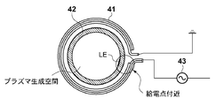
- Patent Document 1 discloses a configuration in which an antenna 41 is wound around a bell jar 42 as shown in FIG. A high frequency voltage is applied from the high frequency power supply 43 to generate plasma in a plasma generation space in the bell jar 42.
- the bell jar 42 is made of an insulating material such as quartz glass, and the outer surface of the bell jar 42 is covered with an insulating film that blocks ultraviolet light, so that ultraviolet light emitted from plasma is emitted. Is shut off.
- the electric field strength is locally high (electric field is concentrated) in the vicinity of the feeding point where the high frequency voltage is applied from the high frequency power supply 43. If the state where the electric field is concentrated continues, (1) local scraping (LE) of the bell jar may occur near the feeding point, and the replacement cycle of the bell jar 42 may be shortened. (2) In addition, when particles are generated by local scraping (LE) of the bell jar 42, the particles may adhere to the surface of the substrate disposed in the substrate processing chamber. (3) Further, due to local scraping (LE) of the bell jar 42, a high impedance portion and a low impedance portion are generated, and the distribution of plasma generated in the bell jar 42 may be non-uniform.
- the bell jar 42 is made of an insulating material such as quartz glass, and even if the insulating bell jar 42 is covered with an insulating film, the electrical characteristics do not change. For this reason, the state where the electric field strength is locally high in the vicinity of the feeding point is not solved even if the insulating film is covered, and the above problems (1) to (3) are still not solved.
- the present invention has been made in view of the above problems, and provides a technique that is excellent in productivity, can suppress the generation of particles in a space for processing a substrate, or can improve the uniformity of plasma generation. For the purpose.
- a substrate processing apparatus is a substrate processing apparatus for processing a substrate with plasma, A first container member that forms a processing space for processing a substrate, and a second container that forms a plasma generation space for plasma generation that is attached to the first container member and communicates with the processing space
- a container having a member A gas introduction part for introducing gas into the container;
- a plasma generation unit provided in an external space of the container and having an antenna that excites the gas in the plasma generation space by an electric field generated by feeding a high-frequency voltage from a power source;
- a substrate holding part capable of holding the substrate in the processing space, A coating film containing a semiconductor material is formed on the surface of the second container member disposed at a position close to the antenna.
- a technology that is excellent in productivity, can suppress the generation of particles in a space for processing a substrate, and can improve the uniformity of plasma generation.
- the substrate processing apparatus 100 includes a container 101 as a configuration for isolating a space for processing the substrate SB from the external space S3 at atmospheric pressure.
- the container 101 includes a diffusion chamber (hereinafter referred to as a first container member) 102 and a bell jar (hereinafter referred to as a second container member) 104.
- the first container member (diffusion chamber) 102 forms a processing space S1 for processing the substrate SB.
- the second container member (belger) 104 forms a plasma generation space S2 for plasma generation that communicates with the processing space S1 in a state of being attached to the first container member.
- the first container member (diffusion chamber) 102 is supported by the base member 103.
- a shield member 114 is attached to the inner wall of the first container member (diffusion chamber) 102 to prevent reaction products generated by plasma from adhering to the inner wall of the first container member (diffusion chamber) 102. It has been.
- the shield member 114 is detachable to enable efficient maintenance work.
- a substrate holding unit 106 capable of holding the substrate SB is provided.
- the substrate holding unit 106 includes an electrode for electrostatically attracting the substrate SB or applying a bias to the substrate SB, and the electrode is connected to the high-frequency power source 133 via the matching unit 131.
- the base member 103 is provided with an exhaust pipe 110.
- the exhaust pipe 110 includes an exhaust device 112 including a vacuum pump capable of reducing the processing space S1 and the plasma generation space S2 to a predetermined degree of vacuum. It is connected.
- the second container member (belger) 104 has a side wall part 120 and a ceiling part 122, and the ceiling part 122 is formed on the upper end side of the side wall part 120.
- the side wall part 120 and the ceiling part 122 are integrally formed.
- the lower end side of the side wall 120 is open, and the plasma generation space S2 and the processing space S1 can communicate with each other through this opening.
- a flange 124 is formed on the outer peripheral side in the vicinity of the opening of the side wall 120, and a seal member such as an O-ring is disposed on the seal surface 126 of the flange 124, for example.
- a seal member such as an O-ring is disposed on the seal surface 126 of the flange 124, for example.
- the gas introduction unit G-IN introduces gas into the container 101.
- a gas containing alcohol can be used alone, or a mixed gas to which an inert gas such as argon gas is added can be used.
- the antenna 130 is disposed in the external space S3 in the vicinity of the second container member (Bellja) 104 constituting the container 101.
- a high frequency voltage is supplied to the antenna 130 from a high frequency power supply 134 via a matching unit 132.
- the matching unit 132 performs impedance matching in order to efficiently supply high-frequency power to the plasma generation space S2 via the antenna even if the configuration on the second container member 104 side or the plasma in the plasma generation space S2 changes. .
- an induction electric field (hereinafter, referred to as an electric field) is generated in the plasma generation space S2 in the second container member (belger) 104.
- the gas introduced by the gas introduction part G-IN is excited in the plasma generation space by this induction electric field, and inductively coupled plasma (hereinafter “plasma”) is generated.
- An electromagnet 139 is disposed on the outer periphery of the antenna 130, and the electromagnet 139 diffuses the plasma in the plasma generation space S2 toward the substrate SB in the processing space S1.
- the antenna 130, the matching unit 132, the high frequency power source 134, and the electromagnet 139 function as a plasma generation unit for generating plasma in the plasma generation space S2.
- the second container member (belger) 104 is made of, for example, an insulating material such as quartz glass.
- the ultraviolet light passes through the second container member (belger) 104, the ultraviolet light and oxygen in the external space S3 are used. Can react to generate ozone.
- the second container member (belger) 104 is disposed at a position close to the antenna 130 disposed in the external space S3 at atmospheric pressure, and a coating film containing a semiconductor material on the surface of the second container member Is formed.
- the coating film containing the semiconductor material mitigates the concentration of the electric field generated at the feeding point of (i) the second container member (Bellja) 104 leaking to the external space S3 and (ii) the high-frequency voltage feed point. In particular, an advantageous effect is realized.
- FIG. 2 shows an example in which a coating film 200 of a semiconductor material is formed on the outer surface of the second container member (belger) 104.
- pretreatment is performed on the outer surface of the second container member (belger) 104. As a result, the outer surface is roughened by blasting.
- the coating film 200 is formed on the second container member (belger) 104 by thermal spraying.
- the semiconductor material thermal spraying material
- the semiconductor material thermal spraying material
- the thermal spraying process is advantageous in terms of reducing heat input to the second container member (belger) 104 and reducing the thermal influence on the second container member (belger) 104 as compared to the welding process. is there.
- the thermal spraying process is an advantageous process in that it can be applied only to a specific portion of the second container member (belger) 104 by masking, as in the coating process.
- a semiconductor material (spraying material) is sprayed and solidified on the outer surface of the second container member (belger) 104 roughened by blasting.
- sufficient engagement between the roughened surface irregularities and the particles of the semiconductor material (spraying material) is ensured, and the second container member (Bellja) 104 and the semiconductor material (spraying material) are in close contact with each other. The strength is improved.
- the coating range where the coating film 200 is formed is the outer surface of the second container member (belger) 104 excluding the seal surface 126.
- the seal surface 126 is excluded from the coverage area by masking. The reason why the sealing surface 126 is excluded from the covering range is that the following two points are taken into consideration.
- (I) It is considered that the sealing performance is lowered due to the formation of the coating film 200.
- the second container member (bell jar) 104 is attached to the first container member (diffusion chamber) 102 (FIG. 1) via a seal member (for example, an O-ring) that is an elastic member. For this reason, even if the coating film 200 is formed on the seal surface 126, it is considered that the effect of blocking ultraviolet light is considered to be lower than that of other outer surfaces.
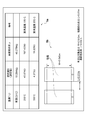
- FIG. 5 is a diagram showing the measurement results of the surface resistance when silicon (Si) is used as the semiconductor material for the thermal spraying process.
- Measurement object Sample (50 mm x 50 mm) sprayed with silicon (Si)
- Measuring equipment HIOKI 3522-50 LCR HiTESTER Shimadzu GAS CHROMATOGRAPH GC-12A (constant temperature bath)
- METEX M-3850D Thermocouple meter
- Measurement voltage 1V Except at room temperature (23 ° C. (room temperature)), a sample placed on a measurement jig (not shown) was placed in a thermostatic bath, and the resistance value R at that time was measured while gradually raising the temperature to the above measurement temperature. .
- the measurement target length W is 0.045 m (45 mm) and the length L between electrodes is 0.01 m (10 mm).
- ⁇ Bermja sprayed with Si is heated more and more during the process. Depending on the process, the temperature may exceed 300 ° C. during use, and it has been confirmed that the plasma is maintained without disappearing. If the resistance value is too low, it will be difficult to maintain a stable plasma, but even if Si is heated and the resistance value decreases, the plasma can be stably maintained at about 350 ° C.
- the coating film 200 containing the semiconductor material By forming the coating film 200 containing the semiconductor material on the outer surface of the second container member (Bellja) 104, ultraviolet light emitted from the plasma can be blocked. Thereby, it is possible to prevent ozone from being generated due to a reaction between ultraviolet light and oxygen in the atmosphere outside the substrate processing apparatus 100.
- FIG. 2 shows an example in which the coating film 200 containing a semiconductor material is directly coated on the second container member (belger) 104, but the gist of the present invention is limited to this example. It is not a thing.
- an insulating film may be coated on the second container member (belger) 104 as an intermediate layer, and the coating film 200 containing a semiconductor material may be coated on the intermediate layer.
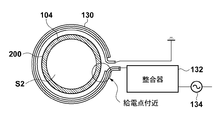
- FIG. 3 is a view showing an AA cross section of the second container member (belger) 104 in FIG. 2, the matching unit 132, and the high frequency power source 134.
- the antenna 130 shows a case of one turn.
- the antenna 130 has two terminals, a power supply terminal that receives high-frequency voltage power supply and a ground terminal that is grounded, and is disposed close to the outer periphery of the second container member (belger) 104.
- the coating film 200 of the semiconductor material By forming the coating film 200 of the semiconductor material on the outer surface of the second container member (belger) 104, the concentration of the electric field generated in the vicinity of the power supply terminal (near the power supply point) that is the power supply point of the high-frequency voltage is reduced to the second. Can be dispersed over the surface of the container member (bell jar) 104.
- the metal film of the conductor When the metal film of the conductor is formed on the outer surface of the second container member (bell jar) 104, electricity flows through the metal film, and electric power is generated inside the second container member (bell jar) 104 by electromagnetic induction. The problem of not being supplied can arise.
- the second container member 104 is formed with an insulating material film
- the second container member (belger) 104 itself is also made of an insulating material such as quartz. Even if it is coated, the electrical characteristics cannot change. For this reason, the metal film of the conductor and the film of the insulating material cannot alleviate the concentration of the electric field generated in the vicinity of the feeding point with respect to the second container member (bell jar) 104.
- the semiconductor material used as the coating film 200 has, for example, an electrical characteristic in which the volume resistivity R is in the range of 1.5 ⁇ 10 ⁇ 5 ⁇ m (1.5 ⁇ 10E- 5 ⁇ m) ⁇ R ⁇ 4000 ⁇ m.
- a semiconductor material for example, silicon
- a material for example, quartz
- the coating film 200 is formed on the outer surface of the second container member (belger) 104
- the gist of the present invention is not limited to this example, and the coating film Even if 200 is formed on the inner surface of the second container member (belger) 104, the same effect can be obtained.
- the substrate processing apparatus 100 of the present embodiment has an advantageous effect of blocking ultraviolet light emitted from the plasma and dispersing the concentration of the electric field generated in the vicinity of the feeding point over the surface of the second container member (Bellja) 104. Realize. By distributing the concentration of the electric field over the surface of the second container member 104, the occurrence of local scraping in the second container member (belger) 104 is suppressed, and the replacement cycle of the second container member 104 is extended. Can be Alternatively, particles generated in the plasma generation space S2 can be reduced by suppressing the occurrence of local shaving in the second container member (belger) 104. Alternatively, plasma with a uniform distribution can be generated in the second container member (belger) 104. According to the substrate processing apparatus 100 according to the present embodiment, it is possible to realize a substrate processing technique with high quality and excellent productivity.
- the substrate processing apparatus 100 is advantageous for substrate processing for manufacturing devices such as semiconductors and liquid crystals.
- the device manufacturing method includes a holding process of holding the substrate by the substrate holding unit 106 of the substrate processing apparatus 100 and an introducing process of introducing gas into the container 101 by the gas introducing unit G-IN of the substrate processing apparatus 100.
- the device manufacturing method includes a generation step of generating plasma by exciting a gas with the plasma generation unit of the substrate processing apparatus 100, and a processing step of processing the substrate with plasma.
Landscapes
- Physics & Mathematics (AREA)
- Engineering & Computer Science (AREA)
- Plasma & Fusion (AREA)
- Chemical & Material Sciences (AREA)
- Analytical Chemistry (AREA)
- Electromagnetism (AREA)
- Spectroscopy & Molecular Physics (AREA)
- Plasma Technology (AREA)
- Chemical Vapour Deposition (AREA)
- Drying Of Semiconductors (AREA)
Abstract
Description
基板を処理するための処理空間を形成する第1の容器部材と、前記第1の容器部材に取付けられた状態で前記処理空間と連通するプラズマ生成用のプラズマ生成空間を形成する第2の容器部材と、を有する容器と、
前記容器にガスを導入するガス導入部と、
前記容器の外部空間に設けられ、電源からの高周波電圧の給電による電界で前記プラズマ生成空間内の前記ガスを励起するアンテナを有するプラズマ生成部と、
前記処理空間において前記基板を保持することが可能な基板保持部と、を備え、
前記アンテナと近接した位置に配置されている前記第2の容器部材の表面に半導体材料を含有する被覆膜が形成されていることを特徴とする。
本発明の実施形態にかかる基板処理装置100の概略構成を、図1を参照しながら説明する。基板処理装置100は、大気圧の外部空間S3から基板SBを処理するための空間を隔離するための構成として容器101を備える。容器101は、拡散チャンバー(以下、第1の容器部材)102と、ベルジャ(以下、第2の容器部材)104と、を有する。第1の容器部材(拡散チャンバー)102は、基板SBを処理するための処理空間S1を形成する。第2の容器部材(ベルジャ)104は、第1の容器部材に取付けられた状態で処理空間S1と連通するプラズマ生成用のプラズマ生成空間S2を形成する。第1の容器部材(拡散チャンバー)102はベース部材103により支持されている。
第2の容器部材(ベルジャ)104は、大気圧の外部空間S3に配置されているアンテナ130に近接した位置に配置されており、第2の容器部材の表面に半導体材料を含有する被覆膜が形成されている。半導体材料を含有する被覆膜は、(i)第2の容器部材(ベルジャ)104から外部空間S3に漏れ出る紫外光の遮断、および(ii)高周波電圧の給電点に生じる電界の集中を緩和するという点で特に有利な効果を実現する。
(2)測定装置:HIOKI 3522-50 LCR HiTESTER
Shimadzu GAS CHROMATOGRAPH GC-12A(恒温槽)
METEX M-3850D(熱電対計)
(3)測定条件
・測定温度:23℃(室温)、200℃、350℃
・測定電圧:1V
常温時(23℃(室温))を除き、測定治具(不図示)に設置した試料を恒温槽に入れ、段階的に温度を上記の測定温度に上げながら、その時の抵抗値Rを測定した。
上記の基板処理装置100は、半導体や液晶などのデバイスを製造するための基板処理に有利である。デバイスの製造方法としては、基板処理装置100の基板保持部106により基板を保持する保持工程と、基板処理装置100のガス導入部G-INにより容器101にガスを導入する導入工程とを有する。また、デバイスの製造方法は、基板処理装置100のプラズマ生成部によりガスを励起してプラズマを生成する生成工程と、プラズマで基板を処理する処理工程と、を有する。
Claims (4)
- プラズマで基板を処理する基板処理装置であって、
基板を処理するための処理空間を形成する第1の容器部材と、前記第1の容器部材に取付けられた状態で前記処理空間と連通するプラズマ生成用のプラズマ生成空間を形成する第2の容器部材と、を有する容器と、
前記容器にガスを導入するガス導入部と、
前記容器の外部空間に設けられ、電源からの高周波電圧の給電による電界でプラズマ生成空間内の前記ガスを励起するアンテナを有するプラズマ生成部と、
前記処理空間において前記基板を保持することが可能な基板保持部と、を備え、
前記アンテナと近接した位置に配置されている前記第2の容器部材の表面に半導体材料を含有する被覆膜が形成されていることを特徴とする基板処理装置。 - 前記被覆膜の体積抵抗率Rの範囲は、1.5×10⁻⁵Ωm≦R≦4000Ωmであることを特徴とする請求項1に記載の基板処理装置。
- 前記第2の容器部材は絶縁材料で形成されており、外側表面にブラスト処理が施され、
前記被覆膜は、前記ブラスト処理が施された前記第2の容器部材の外側表面に形成されていることを特徴とする請求項1または2に記載の基板処理装置。 - 前記被覆膜には、シリコンが含有されていることを特徴とする請求項1乃至3のいずれか1項に記載の基板処理装置。
Priority Applications (4)
| Application Number | Priority Date | Filing Date | Title |
|---|---|---|---|
| KR1020137028218A KR20130135981A (ko) | 2011-03-31 | 2012-03-07 | 기판 처리 장치 |
| CN2012800156023A CN103460812A (zh) | 2011-03-31 | 2012-03-07 | 基板处理装置 |
| JP2013507120A JP5650837B2 (ja) | 2011-03-31 | 2012-03-07 | 基板処理装置 |
| US14/034,636 US20140020833A1 (en) | 2011-03-31 | 2013-09-24 | Substrate processing apparatus |
Applications Claiming Priority (2)
| Application Number | Priority Date | Filing Date | Title |
|---|---|---|---|
| JP2011079700 | 2011-03-31 | ||
| JP2011-079700 | 2011-03-31 |
Related Child Applications (1)
| Application Number | Title | Priority Date | Filing Date |
|---|---|---|---|
| US14/034,636 Continuation US20140020833A1 (en) | 2011-03-31 | 2013-09-24 | Substrate processing apparatus |
Publications (1)
| Publication Number | Publication Date |
|---|---|
| WO2012132253A1 true WO2012132253A1 (ja) | 2012-10-04 |
Family
ID=46930048
Family Applications (1)
| Application Number | Title | Priority Date | Filing Date |
|---|---|---|---|
| PCT/JP2012/001571 Ceased WO2012132253A1 (ja) | 2011-03-31 | 2012-03-07 | 基板処理装置 |
Country Status (6)
| Country | Link |
|---|---|
| US (1) | US20140020833A1 (ja) |
| JP (1) | JP5650837B2 (ja) |
| KR (1) | KR20130135981A (ja) |
| CN (1) | CN103460812A (ja) |
| TW (1) | TWI495002B (ja) |
| WO (1) | WO2012132253A1 (ja) |
Families Citing this family (2)
| Publication number | Priority date | Publication date | Assignee | Title |
|---|---|---|---|---|
| CN103477721B (zh) | 2011-04-04 | 2016-05-18 | 佳能安内华股份有限公司 | 处理装置 |
| TWI483283B (zh) * | 2013-03-08 | 2015-05-01 | Archers Inc | 電力導入裝置及其相關電漿系統 |
Citations (4)
| Publication number | Priority date | Publication date | Assignee | Title |
|---|---|---|---|---|
| JPH08330285A (ja) * | 1995-06-01 | 1996-12-13 | Dainippon Screen Mfg Co Ltd | プラズマ処理装置 |
| JPH10163180A (ja) * | 1996-10-02 | 1998-06-19 | Matsushita Electron Corp | 電子デバイスの製造装置及び電子デバイスの製造方法 |
| JP2009026885A (ja) * | 2007-07-18 | 2009-02-05 | Tokyo Electron Ltd | プラズマ処理装置及びプラズマ生成室 |
| WO2009142016A1 (ja) * | 2008-05-22 | 2009-11-26 | 株式会社イー・エム・ディー | プラズマ生成装置およびプラズマ処理装置 |
Family Cites Families (6)
| Publication number | Priority date | Publication date | Assignee | Title |
|---|---|---|---|---|
| JPH07254499A (ja) * | 1994-03-15 | 1995-10-03 | Hitachi Ltd | マイクロ波プラズマ処理装置 |
| TW279240B (en) * | 1995-08-30 | 1996-06-21 | Applied Materials Inc | Parallel-plate icp source/rf bias electrode head |
| US6056848A (en) * | 1996-09-11 | 2000-05-02 | Ctp, Inc. | Thin film electrostatic shield for inductive plasma processing |
| WO1998051127A1 (en) * | 1997-05-06 | 1998-11-12 | Thermoceramix, L.L.C. | Deposited resistive coatings |
| US6447637B1 (en) * | 1999-07-12 | 2002-09-10 | Applied Materials Inc. | Process chamber having a voltage distribution electrode |
| US6577113B2 (en) * | 2001-06-06 | 2003-06-10 | Tokyo Electron Limited | Apparatus and method for measuring substrate biasing during plasma processing of a substrate |
-
2012
- 2012-03-07 JP JP2013507120A patent/JP5650837B2/ja active Active
- 2012-03-07 KR KR1020137028218A patent/KR20130135981A/ko not_active Ceased
- 2012-03-07 CN CN2012800156023A patent/CN103460812A/zh active Pending
- 2012-03-07 WO PCT/JP2012/001571 patent/WO2012132253A1/ja not_active Ceased
- 2012-03-28 TW TW101110815A patent/TWI495002B/zh active
-
2013
- 2013-09-24 US US14/034,636 patent/US20140020833A1/en not_active Abandoned
Patent Citations (4)
| Publication number | Priority date | Publication date | Assignee | Title |
|---|---|---|---|---|
| JPH08330285A (ja) * | 1995-06-01 | 1996-12-13 | Dainippon Screen Mfg Co Ltd | プラズマ処理装置 |
| JPH10163180A (ja) * | 1996-10-02 | 1998-06-19 | Matsushita Electron Corp | 電子デバイスの製造装置及び電子デバイスの製造方法 |
| JP2009026885A (ja) * | 2007-07-18 | 2009-02-05 | Tokyo Electron Ltd | プラズマ処理装置及びプラズマ生成室 |
| WO2009142016A1 (ja) * | 2008-05-22 | 2009-11-26 | 株式会社イー・エム・ディー | プラズマ生成装置およびプラズマ処理装置 |
Also Published As
| Publication number | Publication date |
|---|---|
| TWI495002B (zh) | 2015-08-01 |
| US20140020833A1 (en) | 2014-01-23 |
| JP5650837B2 (ja) | 2015-01-07 |
| TW201301387A (zh) | 2013-01-01 |
| KR20130135981A (ko) | 2013-12-11 |
| JPWO2012132253A1 (ja) | 2014-07-24 |
| CN103460812A (zh) | 2013-12-18 |
Similar Documents
| Publication | Publication Date | Title |
|---|---|---|
| US9574270B2 (en) | Plasma processing apparatus | |
| JP5606821B2 (ja) | プラズマ処理装置 | |
| US8800484B2 (en) | Plasma processing apparatus | |
| TWI734185B (zh) | 電漿處理裝置 | |
| US20070215279A1 (en) | Plasma processing apparatus, plasma processing method, focus ring, and focus ring component | |
| US20230061699A1 (en) | Upper electrode and plasma processing apparatus | |
| US20090291563A1 (en) | Plasma processing apparatus and plasma processing method | |
| JP2010103455A (ja) | プラズマ処理装置 | |
| JP3050124B2 (ja) | プラズマ処理装置 | |
| TW201401425A (zh) | 針對被處理基體之微粒附著控制方法及處理裝置 | |
| JP5650837B2 (ja) | 基板処理装置 | |
| KR102229990B1 (ko) | 플라즈마 처리 장치용 부재 및 플라즈마 처리 장치 | |
| JP2002155371A (ja) | 半導体素子の製造方法及びその装置 | |
| TWI517243B (zh) | 電漿處理裝置 | |
| JP2008251857A (ja) | プラズマ処理装置 | |
| JP2002203836A (ja) | プラズマ処理方法及びプラズマ処理装置 | |
| JP2016058536A (ja) | プラズマ処理装置及びクリーニング方法 | |
| JP2007324186A (ja) | プラズマ処理装置 | |
| JP7182916B2 (ja) | プラズマ処理装置 | |
| WO2009116579A1 (ja) | プラズマ処理方法及びプラズマ処理装置 | |
| JP2006253312A (ja) | プラズマ処理装置 | |
| JP2007243020A (ja) | プラズマ処理装置 | |
| JP4143362B2 (ja) | プラズマ処理装置 | |
| TW202613356A (zh) | 成膜方法、保護膜及基板處理裝置 | |
| JP2026017627A (ja) | 成膜方法、保護膜及び基板処理装置 |
Legal Events
| Date | Code | Title | Description |
|---|---|---|---|
| 121 | Ep: the epo has been informed by wipo that ep was designated in this application |
Ref document number: 12762761 Country of ref document: EP Kind code of ref document: A1 |
|
| DPE1 | Request for preliminary examination filed after expiration of 19th month from priority date (pct application filed from 20040101) | ||
| ENP | Entry into the national phase |
Ref document number: 2013507120 Country of ref document: JP Kind code of ref document: A |
|
| NENP | Non-entry into the national phase |
Ref country code: DE |
|
| ENP | Entry into the national phase |
Ref document number: 20137028218 Country of ref document: KR Kind code of ref document: A |
|
| 122 | Ep: pct application non-entry in european phase |
Ref document number: 12762761 Country of ref document: EP Kind code of ref document: A1 |