WO2012132217A1 - Can通信システム、can送信装置、can受信装置、およびcan通信方法 - Google Patents
Can通信システム、can送信装置、can受信装置、およびcan通信方法 Download PDFInfo
- Publication number
- WO2012132217A1 WO2012132217A1 PCT/JP2012/001281 JP2012001281W WO2012132217A1 WO 2012132217 A1 WO2012132217 A1 WO 2012132217A1 JP 2012001281 W JP2012001281 W JP 2012001281W WO 2012132217 A1 WO2012132217 A1 WO 2012132217A1
- Authority
- WO
- WIPO (PCT)
- Prior art keywords
- bit
- logical value
- data
- transmission
- bits
- Prior art date
- Legal status (The legal status is an assumption and is not a legal conclusion. Google has not performed a legal analysis and makes no representation as to the accuracy of the status listed.)
- Ceased
Links
Images






Classifications
-
- H—ELECTRICITY
- H04—ELECTRIC COMMUNICATION TECHNIQUE
- H04L—TRANSMISSION OF DIGITAL INFORMATION, e.g. TELEGRAPHIC COMMUNICATION
- H04L12/00—Data switching networks
- H04L12/28—Data switching networks characterised by path configuration, e.g. LAN [Local Area Networks] or WAN [Wide Area Networks]
- H04L12/40—Bus networks
- H04L12/407—Bus networks with decentralised control
- H04L12/413—Bus networks with decentralised control with random access, e.g. carrier-sense multiple-access with collision detection [CSMA-CD]
-
- H—ELECTRICITY
- H04—ELECTRIC COMMUNICATION TECHNIQUE
- H04J—MULTIPLEX COMMUNICATION
- H04J3/00—Time-division multiplex systems
- H04J3/02—Details
- H04J3/06—Synchronising arrangements
- H04J3/0635—Clock or time synchronisation in a network
- H04J3/0638—Clock or time synchronisation among nodes; Internode synchronisation
-
- H—ELECTRICITY
- H04—ELECTRIC COMMUNICATION TECHNIQUE
- H04J—MULTIPLEX COMMUNICATION
- H04J3/00—Time-division multiplex systems
- H04J3/02—Details
- H04J3/06—Synchronising arrangements
- H04J3/0635—Clock or time synchronisation in a network
- H04J3/0638—Clock or time synchronisation among nodes; Internode synchronisation
- H04J3/0658—Clock or time synchronisation among packet nodes
-
- H—ELECTRICITY
- H04—ELECTRIC COMMUNICATION TECHNIQUE
- H04L—TRANSMISSION OF DIGITAL INFORMATION, e.g. TELEGRAPHIC COMMUNICATION
- H04L1/00—Arrangements for detecting or preventing errors in the information received
- H04L1/20—Arrangements for detecting or preventing errors in the information received using signal quality detector
- H04L1/205—Arrangements for detecting or preventing errors in the information received using signal quality detector jitter monitoring
-
- H—ELECTRICITY
- H04—ELECTRIC COMMUNICATION TECHNIQUE
- H04L—TRANSMISSION OF DIGITAL INFORMATION, e.g. TELEGRAPHIC COMMUNICATION
- H04L12/00—Data switching networks
- H04L12/28—Data switching networks characterised by path configuration, e.g. LAN [Local Area Networks] or WAN [Wide Area Networks]
- H04L12/40—Bus networks
- H04L12/40006—Architecture of a communication node
- H04L12/40013—Details regarding a bus controller
Definitions
- the present invention relates to a CAN communication system, a CAN transmission device, a CAN reception device, and a CAN communication method.
- Patent Document 1 discloses a CAN (Controller Area Network) basic patent.
- CAN Controller Area Network
- data transmission / reception between the transmission side and the reception side is synchronized by performing resynchronization during communication between the transmission side and the reception side.
- the mechanism of resynchronization in the CAN protocol will be specifically described.
- FIG. 13 is a diagram showing a change in data length per bit when jitter occurs in the CAN protocol.
- the data per bit in the CAN protocol bitstream includes a synchronization segment SYNC, a propagation time segment PROP, a phase buffer segment PHASE1, and a phase buffer segment PHASE2. Between the phase buffer segment PHASE1 and the phase buffer segment PHASE2, there is a sample point for sampling data.
- the upper diagram of FIG. 13 shows the data length per bit recognized based on an ideal clock.
- the lower diagram of FIG. 13 shows the data length per bit recognized based on the clock delayed by jitter.
- df shown in the lower diagram of FIG. 13 indicates a jitter ratio based on an ideal clock length.
- Bit stuffing is a protocol in which one bit is inserted after inverting the logical value when the same logical value continues for 5 bits on the bitstream. Thereby, continuation of the same logical value can be suppressed.
- Patent Document 2 discloses a technique related to resynchronization.
- the vehicular data transmission system according to this technique detects a period in which the same logic continues, and sets a resynchronization range of the data signal according to the detected period.
- the bit stuffing mechanism inserts a stuff bit that takes the inverted value of the logical value when the same logical value continues for 5 bits on the bit stream.
- the resynchronization interval is 10 bits at the longest.
- the width from when a low stuff bit is inserted after 5 low bits are inserted continuously until a falling edge is formed after a low stuff bit is inserted after 5 high bits again. This is because the width is 10 bits.
- the CAN communication system provides bit data in which a plurality of bits each taking either a first logical value or a second logical value obtained by inverting the first logical value are consecutive.
- bit data in which a stuff bit having an inverted value of the same logical value is inserted next to the bit data having a predetermined number of consecutive consecutive logical values.
- a receiving device that executes synchronization processing for synchronizing transmission and reception of the transmission data with the transmitting device, wherein the transmitting device includes the bit data In the bit data, one bit of the predetermined number minus 1 bit is continuously added to the first logical value after the bit following the predetermined number of consecutive bits in the bit data. And a transmission control unit for rewriting the data.
- the CAN transmission device is based on a CAN (Controller Area Network) protocol from a second logical value obtained by inverting a first logical value in received data to the first logical value.
- a plurality of bits each taking either the first logical value or the second logical value are continuous in a receiving apparatus that executes a synchronization process for synchronizing the transmission and reception of data in response to detection of an edge.
- bit data When transmitting bit data, based on the CAN protocol, transmission data in which a stuff bit having an inverted value of the same logical value is inserted next to a predetermined number of consecutive bits having the same logical value in the bit data
- a transmission device that transmits instead of the bit data, wherein when transmitting the bit data, a predetermined number of the first logical values are consecutive in the bit data.
- a control unit that rewrites any one of the predetermined number minus 1 bit to the first logical value in succession from the bit next to the succeeding bit.
- the transmitting device has a plurality of consecutive bits each taking either the first logical value or the second logical value obtained by inverting the first logical value.
- a stuff bit that takes the inverted value of the same logical value is next to a bit in which the same logical value continues for a predetermined number of times in the bit data.
- the inserted transmission data is received from the transmission device instead of the bit data, and an edge from the second logical value to the first logical value in the transmission data is detected based on the CAN protocol.
- a receiving device that executes a synchronization process for synchronizing transmission and reception of the transmission data with the transmitting device, wherein the receiving device detects the second logical value.
- the edge to the first logical value follows from the second logical value after the bit in which the first logical value continues for a predetermined number of times in the bit data when the transmitting device transmits the bit data. Including an edge to the first logical value in which any one of the predetermined number minus 1 bit is rewritten.
- bit data in which a plurality of bits each taking either the first logical value or the second logical value obtained by inverting the first logical value is stored.
- transmission data in which a stuff bit having an inverted value of the same logical value is inserted next to the bit data having a predetermined number of consecutive consecutive logical values In response to detection of an edge from the second logical value to the first logical value in the transmission data transmitted from the transmission device based on the CAN protocol, based on the CAN protocol.
- the stuff bit taking the inverted value of the second logical value is inserted.
- An edge from the second logical value to the first logical value can be generated at a position before the first. Therefore, the worst value of the resynchronization interval can be shortened.
- a CAN communication system a CAN transmission device, a CAN reception device, and a CAN communication method that can construct a CAN communication system at low cost using a low-accuracy clock are provided. be able to.
- FIG. 1 is a configuration diagram of a CAN communication system 101 according to the first embodiment of the present invention. In the present embodiment, a case where the CAN communication system 101 is applied to an automobile is illustrated.
- the CAN communication system 101 includes a body system control node 102, a safety system control node 103, an information system control node 104, an engine system control node 105, and a chassis system control node 106.
- the nodes 102 to 106 are connected to each other by a CAN bus, and can transmit / receive arbitrary data to / from each other.
- the body system control node 102 controls body systems such as a headlamp, an air conditioner, and a door based on data received from other nodes.
- the safety system control node 103 controls safety devices such as sensors and airbags based on data received from other nodes.
- the information system control node 104 controls information system devices such as car audio, car radio, and car television based on data received from other nodes.
- the engine system control node 105 controls the engine and engine system devices such as AT (Automatic Transmission) based on data received from other nodes.
- the chassis control node 106 controls chassis devices such as steering and brakes based on data received from other nodes. Further, each of the nodes 102 to 106 transmits data based on the control result to other nodes as necessary.
- FIG. 2 is a configuration diagram of the node 100 according to the first exemplary embodiment of the present invention.
- each of the nodes 102 to 106 has the same configuration as that of the node 100.
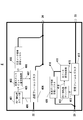
- the node 100 includes a CAN controller LSI (Large Scale Integration) 10 and a bus transceiver 14.
- the CAN controller LSI 10 includes a CAN controller module 1, a CPU (Central Processing Unit) 11, other peripheral modules 12, and an SSCG (Spread Spectrum Model Clock Generator 13).
- the CAN controller module 1 includes a bit stream control unit 2, an error management unit 3, an extended stuff bit control unit 4, a message handler 5, and a message buffer memory 6.
- the CAN controller module 1, the CPU 11, and the other peripheral modules 12 are connected to each other by a local bus 21 and can transmit / receive arbitrary data to / from each other.
- the CAN controller module 1 is accessed from the CPU 11 via the local bus 21.
- the CAN controller module 1 is connected to the CAN bus via the bus transceiver 14.
- the CAN controller module 1 transmits / receives data to / from other nodes in response to a request from the CPU 11.
- the bit stream control unit 2 calculates a CRC (Cyclic Redundancy Check) based on the transmission frame data 24 output from the extended stuff bit control unit 4.
- the bit stream control unit 2 adds a CRC to the transmission frame data 24 in accordance with the CAN protocol frame format.
- the bit stream control unit 2 inserts stuff bits into transmission frame data to which a CRC is added based on bit stuffing defined by the CAN protocol. That is, a stuff bit having a logical value inverted from the logical value is inserted after five consecutive bits having the same logical value.
- the bit stream control unit 2 outputs the transmission frame data in which the stuff bit is inserted to the bus transceiver 14 as a transmission data output (TxD) 31.
- TxD transmission data output
- the bit stream control unit 2 removes the stuff bits defined by the CAN protocol from the received data input (RxD) 30 output from the bus transceiver 14.
- the bit stream control unit 2 performs a CRC check based on the received frame data from which the stuff bits are removed from the received data input (RxD) 30.
- the bit stream control unit 2 detects an abnormality in the CRC check
- the bit stream control unit 2 outputs an abnormality notification signal 26 for notifying the abnormality to the error management unit 3.
- the bit stream control unit 2 removes the CRC from the received frame data after the CRC check.
- the bit stream control unit 2 outputs the received frame data 25 from which the CRC has been removed to the extended stuff bit control unit 4.
- bitstream control unit 2 performs resynchronization defined by the CAN protocol. That is, when the falling edge is detected in the received data input (RxD) 30, the bit stream control unit 2 causes the phase buffer segment PHASE 1 or the phase buffer segment PHASE 2 so that the falling edge is positioned in the synchronization segment SYNC. Is changed by the jump width setting value SJW to adjust the sample point.
- the error management unit 3 performs processing according to the output of the abnormality notification signal 26 from the bit stream control unit 2. This process is, for example, a process in which the error management unit 3 further notifies the CPU 11 of the abnormality, so that the CPU 11 responds to this notification to recover from the abnormality or other peripheral module 12 to recover from the abnormality. You may make it perform control of.
- the extended stuff bit control unit 4 overwrites the extended stuff bit on the transmission frame data 22 output from the message handler 5 based on a method described later. At this time, the extended stuff bit control unit 4 records the original logical value before overwriting the extended stuff bit in the redundant data area of the transmission frame data 24 and stores the transmission frame data 24 after overwriting the extended stuff bit. Output to the bitstream control unit 2.
- the extended stuff bit control unit 4 applies the extended stuff bit to the received frame data 25 output from the bit stream control unit 2 according to the original logical value recorded in the redundant data area based on the method described later. Correct to the original logical value.
- the extended stuff bit control unit 4 outputs the received frame data 23 after correction to the original logical value to the message handler 5.
- the message handler 5 acquires the transmission frame data 22 stored in the transmission buffer of the message buffer memory 6 and transfers it to the extended stuff bit control unit 4. Further, the message handler 5 stores the received frame data 23 output from the extended stuff bit control unit 4 in the reception buffer of the message buffer memory 6.
- the message buffer memory 6 has a reception buffer and a transmission buffer.
- the transmission buffer stores transmission frame data to be transmitted to other nodes.
- the reception buffer stores transmission frame data received from other nodes.
- the message buffer memory 6 has a storage device for constituting a reception buffer and a transmission buffer.
- the storage device is, for example, a register and a memory.
- the CAN controller LSI 10 controls devices included in the node 100. For example, when the node 100 is the engine system control node 105, the engine system device is controlled.
- the CPU 11 controls the devices included in the node 100 by outputting control instruction data for instructing other peripheral modules to control the devices included in the node 100 via the local bus 21.
- CPU11 determines the control content of the apparatus contained in the node 100 based on the data received from the other node, for example.
- the CPU 11 acquires data transmitted from other nodes from the reception buffer of the message buffer memory 6 via the local bus 21.
- the CPU 11 stores data to be transmitted to other nodes via the local bus 21 in the transmission buffer of the message buffer memory 6.
- the other peripheral module 12 controls the devices included in the node 100 based on the control instruction data output from the CPU 11.
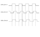
- the SSCG 13 supplies each of the clocks 41 to 43 to each circuit such as the CAN controller module 1, the CPU 11, and the other peripheral modules 12 in the CAN controller LSI 10. That is, in this Embodiment 1, the case where SSCG13 is multi-output SSCG is illustrated. As illustrated in FIG. 3, the SSCG 13 adds jitter to the clock in order to reduce noise in the clock. FIG. 3 illustrates a case where the clock 41 is an ideal clock and the clock 42 and the clock 43 are delayed by jitter. Thus, although the SSCG 13 is low EMI (Electro Magnetic Interference), the accuracy of the clock is lowered.
- EMI Electro Magnetic Interference
- the bus transceiver 14 transmits the transmission data output 31 output from the bit stream control unit 2 to another node as a bit stream.
- the bus transceiver 14 outputs the bit stream received from another node to the bit stream control unit 2 as the reception data input 30.
- FIG. 4 is a configuration diagram of the extended stuff bit control unit 4 according to the first embodiment of the present invention.
- the extended stuff bit control unit 4 includes an identical logical value count unit 401, an extended stuff bit overwrite control unit 402, a redundant data area transmission register 403, a transmission frame register 404, a redundant data area reception register 409, an identical logical value count unit 410, A data restoration control unit 411 and a reception frame register 412 are included.
- the same logical value counting unit 401 counts the number of consecutive identical logical values in the transmission frame bit read value 406 obtained by sequentially reading the transmission frame data 22 stored in the transmission frame register 404 bit by bit from the top.
- the same logical value count unit 401 detects bits having the same logical value for 5 consecutive bits, it outputs a 5-bit continuous identical logical value detection signal 405 to the extended stuff bit overwrite control unit 402.
- the extended stuff bit overwrite control unit 402 receives the same logical value of the transmission frame data 22 stored in the transmission frame register 404 in response to the output of the 5-bit consecutive identical logical value detection signal 405 from the identical logical value count unit 401. Reads the logical value of the next 5 consecutive bits and writes it to the corresponding bit in the redundant data area transmission register 403. Then, the extended stuff bit overwrite control unit 402 overwrites the same logical value of 5 consecutive bits with the next bit of the 5 consecutive bits of the same logical value. That is, the logical value before overwriting is stored in the redundant data area transmission register 403. Further, the overwritten bit becomes an extended stuff bit.
- the redundant data area transmission register 403 stores the logical values before the overwriting of the extended stuff bits as many as the number of extended stuff bits in the transmission frame data 22.
- the extended stuff bit control unit 4 stores the transmission frame data after overwriting the extended stuff bits stored in the transmission frame register 404 and the redundant data area transmission register 403 after the processing on the entire transmission frame data 22 is completed. Data obtained by concatenating the logical values before overwriting of the extended stuff bits is output to the bit stream control unit 2 as transmission frame data 24.
- a portion corresponding to the logical value before overwriting in the transmission frame data 24 is referred to as a redundant data area.
- the redundant data area transmission register 403 stores a logical value before the extension stuff bit is overwritten.
- the redundant data area transmission register 403 stores a logical value before overwriting corresponding to each of the extended stuff bits included in the transmission frame data 22.
- the transmission frame register 407 stores the transmission frame data 22 output from the message handler 5.
- the redundant data area reception register 409 stores redundant data area data among the received frame data 25 output from the bit stream control unit 2. That is, the redundant data area reception register 409 stores the logical value before overwriting corresponding to each of the extended stuff bits included in the reception frame data 25.
- the same logical value count unit 410 counts the number of consecutive identical logical values for the received frame bit read value 413 obtained by reading the data stored in the received frame register 412 bit by bit from the top in order.
- the same logical value count unit 410 detects bits of the same logical value for 5 consecutive bits, it outputs a 5-bit continuous identical logical value detection signal 414 to the original data restoration control unit 411.
- the original data restoration control unit 411 responds to the 5-bit consecutive identical logical value detection signal 414 from the identical logical value count unit 410, and among the logical values of the redundant data area output from the redundant data area reception register 409, A logical value 415 before overwriting of the next extended stuff bit of 5 bits having consecutive logical values is acquired. Then, the original data restoration control unit 411 overwrites the acquired logical value 415 on the extended stuff bit of the reception frame register 412. As a result, the logical value of the extended stuff bit is restored to the original logical value.
- the same logical value count unit 410 and the original data restoration control unit 411 perform this process on the entire data stored in the reception frame register 412.
- the extended stuff bit control unit 4 outputs the restored data stored in the reception frame register 412 to the message handler 5 as reception frame data 23 after the processing on the entire data stored in the reception frame register 412 is completed.
- the received frame register 412 stores data corresponding to the original received frame data 23 excluding the redundant data area in the received frame data 25 output from the bit stream control unit 2.
- FIG. 5 is a flowchart showing a transmission process of the extended stuff bit control unit 4 according to the first embodiment of the present invention.
- the extended stuff bit control unit 4 acquires the transmission frame data 22 from the transmission buffer of the message buffer memory 6 via the message handler 5, and stores it in the transmission frame register 404 (S1).
- the same logical value counting unit 401 reads one bit from the transmission frame data 22 stored in the transmission frame register 404 (S2). Note that 1-bit reading in step S2 and step S6 described later is performed in order from the top of the transmission frame data 22. Therefore, at the first reading, the first bit of the transmission frame data 22 is read. When the bit has already been read, the bit next to the bit read immediately before is read. Here, the order from the top of the transmission frame data 22 is equal to the transmission order of the bits included in the transmission frame data 22. The same logical value counting unit 401 determines whether or not all the transmission frame data 22 stored in the transmission frame register 404 has been read (S3).
- the extended stuff bit control unit 4 executes the process of step S12 described later.
- the same logical value counting unit 401 When it is determined that all the transmission frame data 22 has not been read (S3: No), the same logical value counting unit 401 initializes the count value of the counter to “1” (S4). The same logical value counting unit 401 sets the bit read immediately before as a reference bit that serves as a reference for counting whether or not the same logical value continues for 5 bits (S5). The same logical value counting unit 401 reads one bit from the transmission frame data 22 stored in the transmission frame register 404 (S6). The same logical value counting unit 401 determines whether or not all the transmission frame data 22 stored in the transmission frame register 404 has been read (S7).
- the extended stuff bit control unit 4 executes a process of step S12 described later.
- the same logical value counting unit 401 determines whether or not the reference bit and the bit read immediately before have the same logical value (S8).
- the same logical value count unit 401 restarts the process from step S4. In this case, the same logical value is not continuous. Therefore, the process returns to step S4, and the counting of whether or not the same logical value continues for 5 bits is restarted with the bit read immediately before as the reference bit.
- the same logical value count unit 401 counts up the counter (S9).
- the same logical value counting unit 401 determines whether or not the counter value has reached the threshold value “5” (S10).
- step S6 If the counter value is not equal to the threshold value “5” (S10: No), the same logical value counting unit 401 restarts the process from step S6. In this case, the same logical value continues from the reference bit to the bit read immediately before, but the same logical value has not yet continued for 5 bits. Therefore, returning to step S6, the logical value of the next bit is confirmed.
- the extended stuff bit overwrite control unit 402 reads the logical value of the extended stuff bit next to the bit read immediately before, and writes it in the bit corresponding to the extended stuff bit in the redundant data area transmission register 403. Then, the extended stuff bit overwrite control unit 402 overwrites the extended stuff bit with a logical value of 5 consecutive bits (S11).
- step S2 reads the next extended stuff bit (S2), sets it as a reference bit (S5), and restarts counting whether the same logical value is 5 bits continuous. .
- step S 12 the extended stuff bit control unit 4 generates transmission frame data 24 based on the data stored in the transmission frame register 404 and the data stored in the redundant data area transmission register 403, and sends it to the bit stream control unit 2. Output (S12).
- the transmission process of the extended stuff bit control unit 4 according to the first embodiment of the present invention has been described above. If the process is to overwrite the next five extended stuff bits with the same logical value, the above-described process is performed. It is not limited to a processing procedure, You may change suitably. For example, the reference bit is set and the logical value of the reference bit is compared with the logical value of the bit read immediately before, but the logical value of the bit read immediately before and the bit read before that bit You may make it compare with the logical value of. Further, for example, the execution order of the processes of step S4 and step S5 may be reversed.
- FIG. 6 is a flowchart showing a reception process of the extended stuff bit control unit 4 according to the first embodiment of the present invention.
- the extended stuff bit control unit 4 acquires the reception frame data 25 output from the bit stream control unit 2, and stores the redundant data area data in the received reception frame data 25 in the redundant data area reception register 409. The other data is stored in the reception frame register 412 (S21).
- the same logical value counting unit 410 reads 1 bit from the received frame data 25 stored in the received frame register 412 (S22). Note that 1-bit reading in step S22 and steps S26 and S31 described later is performed in order from the top of the received frame data 25. Therefore, at the first reading, the first bit of the received frame data 25 is read. When the bit has already been read, the bit next to the bit read immediately before is read. Here, the order from the head of the reception frame data 25 is equal to the reception order of the bits included in the reception frame data 25. The same logical value counting unit 410 determines whether all the data stored in the reception frame register 412 has been read (S23).
- the extended stuff bit control unit 4 executes a process of step S33 described later.
- the same logical value counting unit 410 When it is determined that all the data stored in the reception frame register 412 has not been read (S23: No), the same logical value counting unit 410 initializes the count value of the counter to “1” (S24). The same logical value counting unit 410 sets the bit read immediately before as a reference bit that serves as a reference for counting whether or not the same logical value continues for 5 bits (S25). The same logical value counting unit 410 reads one bit from the data stored in the reception frame register 412 (S26). The same logical value counting unit 410 determines whether all the data stored in the reception frame register 412 has been read (S27).
- the extended stuff bit control unit 4 executes a process of step S33 described later.
- the same logical value counting unit 410 determines whether or not the reference bit and the bit read immediately before have the same logical value. (S28).
- the same logical value count unit 410 restarts the process from step S24. In this case, the same logical value is not continuous. Therefore, the process returns to step S24, and the counting of whether or not the same logical value continues for 5 bits is restarted with the bit read immediately before as the reference bit.
- the same logical value count unit 410 counts up the counter (S29). The same logical value counting unit 410 determines whether or not the counter value has reached the threshold value “5” (S30).
- step S26 If the counter value is not equal to the threshold value “5” (S30: No), the same logical value counting unit 410 restarts the process from step S26. In this case, the same logical value continues from the reference bit to the bit read immediately before, but the same logical value has not yet continued for 5 bits. Therefore, the process returns to step S26 to confirm the logical value of the next bit.
- the same logical value continues for 5 bits from the reference bit to the bit read immediately before. That is, the bit next to the bit read immediately before is an extended stuff bit.
- the same logical value count unit 410 reads one bit of the next extended stuff bit from the received frame data 25 stored in the received frame register 412 before the extended stuff bit is restored to the logical value before being overwritten ( S31).
- the original data restoration control unit 411 reads the logical value before overwriting stored in the bit corresponding to the extended stuff bit in the redundant data area reception register 409. Then, the original data restoration control unit 411 overwrites the extended stuff bit of the reception frame register 412 with the read logical value before overwriting (S32).
- step S23 uses the bit read immediately before as the reference bit (S25), and restarts counting whether or not the same logical value continues for 5 bits.
- step S33 the extended stuff bit control unit 4 stores the received frame data 23 generated by returning the extended stuff bit of the received frame data 25 stored in the received frame register 412 to the logical value before overwriting. 5 (S33).
- the reception process of the extended stuff bit control unit 4 according to the first embodiment of the present invention has been described above, but the process of restoring the logical value before overwriting to the next 5-bit extended stuff bit in which the same logical value is continuous
- the reference bit is set and the logical value of the reference bit is compared with the logical value of the read bit.
- the logical value of the bit read immediately before and the logical value of the bit read before that bit are compared. You may make it compare with a value.
- the execution order of the processes of step S24 and step S25 may be reversed.
- Low of the same logical value is forcibly set to the next bit of the 5 bits.
- the bit next to the stuff bit can be set to Low. That is, the falling edge which is the resynchronization edge defined by the CAN protocol is created by overwriting the extended stuff bit immediately after the stuff bit to Low.
- the worst value of the resynchronization interval can be shortened from 10 bits to 6 bits. Therefore, as illustrated with reference to FIG. 3, even if the system is constructed by SSCG, a clock oscillator, or the like that generates a low-accuracy clock, the influence can be reduced. That is, even if an SSCG or a clock oscillator that generates a low-cost but low-accuracy clock is used, a CAN communication system can be constructed. Therefore, according to the first embodiment, a CAN communication system can be constructed at a low cost using a low-accuracy clock.
- the SSCG that intentionally generates a jitter-added clock is effective in reducing EMI noise, but has a problem that it cannot be used easily because the clock error between nodes becomes large. .
- noise can be reduced.
- the frequency band of FM (Frequency Modulation) radio overlaps with the operating frequency of a general MCU (Micro Control Unit), so that it is possible to reduce noise mixed in and improve sound quality. become.
- MCU Micro Control Unit
- harmonic noise has an adverse effect on the UHF (Ultra High Frequency) band.
- UHF Ultra High Frequency
- the next bit of 5 bits having the same logical value is used as an extended stuff bit, and the same logical value having 5 bits is overwritten so that the edge is overwritten.
- the worst value of the resynchronization interval is 10
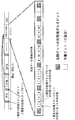
- the bit can be shortened to 9 bits. That is, in the transmission frame data 22, 4 bits (7th to 10th bits in FIG. 7) are consecutive from the next extended stuff bit of 5 bits (the 1st to 5th bits in FIG. 7) having the same logical value.
- the worst value of the resynchronization interval can be shortened by overwriting any one of the bits) with the same logical value of 5 consecutive bits.
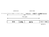
- the redundant data area of the transmission frame data 24 and the reception frame data 25 is indicated by the redundant data area of the transmission frame data 24 and the reception frame data 25.
- a 3-byte redundant data area is defined for transmission frame data 22 having a maximum size of 79 bits.
- the transmission frame data 22 includes a start of frame, an arbitration field Arb, a control field CTRL, and a data field DATA in a CAN protocol data frame.
- the logical value before overwriting is stored so as to correspond to each of the extended stuff bits of the transmission frame data.
- the logical value before overwriting the extended stuff bits is recorded in the maximum 15-bit redundant data area.
- the logical values before overwriting of the extended stuff bits in the order from the beginning to the end of the transmission frame data are stored in the respective bits in the order from the beginning to the end of the redundant data area.
- the present invention is not limited to this as long as the extended stuff bit corresponds to the logical value before overwriting. Note that the order from the beginning to the end is the order of transmission in the case of transmission as a bit stream.
- every 4 bits are provided with a bit whose logical value is the inverted value of the left adjacent bit. That is, in the redundant data area, a bit having an inverted value of the previous bit is provided for every 4 bits. According to this, it is possible to prevent 5 bits of the same logical value from continuing in the redundant data area and to prevent stuff bits from being inserted into the redundant data area. The reason for this is that if it becomes necessary to provide extended stuff bits in the redundant data area, a redundant data area corresponding to the extended stuff bit is required. Further, according to this, the resynchronization interval can be shortened.
- the redundant data area has the maximum 15-bit logical value bit before overwriting and the bit having the logical value of the inverted value of the previous bit every 4 bits. Are defined as 3 bytes long. Note that the size of the redundant data area is limited to the size exemplified here as long as all of these bits can be recorded even when the number of extended stuff bits is the largest based on the maximum size of the transmission frame data 22. I can't.
- FIG. 10 is a configuration diagram of the node 200 according to the second embodiment of the present invention. Note that description of the same contents as those of the node 100 according to the first embodiment is omitted. Moreover, since the structure of the CAN communication system concerning Embodiment 2 of this invention is the same as that of Embodiment 1, description is abbreviate
- the node 200 is different from the node 100 according to the first embodiment in that the node 200 does not include the extended stuff bit control unit 4 but includes the bit stream control unit 7 instead of the bit stream control unit 2.
- the bitstream control unit 7 further performs resynchronization at the rising edge. That is, the bit stream control unit 7 performs resynchronization at the rising edge in addition to resynchronization at the falling edge determined by the CAN protocol. Further, the message handler 5 transmits and receives transmission frame data 22 and reception frame data between the bit stream control unit 7 and the message buffer memory 6.
- FIG. 11 is a configuration diagram of the bit stream control unit 7 according to the second embodiment of the present invention.
- the bit stream control unit 7 includes a CRC encoding unit 701, a frame format shaping output control unit 702, a transmission shift register 703, both rising and falling edge detection circuits 704, a bit resynchronization control unit 705, a bit sampling unit 706, a reception shift register 707, a CRC decoding and stuff bit removing unit 708, a flip-flop group 709, and a protocol control state machine 710.
- the CRC encoding unit 701 generates a CRC based on the transmission frame data 22 output from the transmission shift register 703.
- the CRC encoding unit 701 outputs the generated CRC to the transmission shift register 703.
- the frame format shaping output control unit 702 inserts stuff bits into the data 711 output from the transmission shift register 703 and outputs the data 711 to the bus transceiver 14 as a transmission data output (TXD) 31.
- the transmission shift register 703 sequentially outputs the transmission frame data 22 output from the message handler 5 to the CRC encoding unit 701 and the sequential frame format shaping output control unit 702 bit by bit. Also, the transmission shift register 703 continues the transmission frame data 22 and sequentially outputs the CRC output from the CRC encoding unit 701 to the frame format shaping output control unit 702 bit by bit.
- the rising / falling edge detection circuit 704 detects the rising edge and the falling edge of the received data input (RxD) 30.
- the rising / falling edge detection circuit 704 outputs a bit resynchronization trigger signal 713 to the bit resynchronization control unit 705 when detecting either a rising edge or a falling edge.
- the rising / falling edge detection circuit 704 uses an XOR circuit to perform XOR between the logical value of an arbitrary bit of the received data input (RxD) 30 and the logical value of the bit next to that bit. By performing the operation, the logical value of each bit is different, and it is detected that a rising edge or a falling edge has occurred.
- both the rising and falling edge detection circuit 704 inputs the logical value of each bit to the XOR circuit, and resynchronizes the high signal output from the XOR circuit when the logical value of each bit is different.
- the trigger signal 713 is output to the bit resynchronization control unit 705.
- the bit resynchronization control unit 705 outputs a bit timing signal 714 to the bit sampling unit 706 for each sample point. Further, the bit resynchronization control unit 705 performs resynchronization in accordance with the bit resynchronization trigger signal 713 output from the rising / falling edge detection circuit 704. In other words, the bit resynchronization control unit 705 corrects the sample point based on the output timing of the bit resynchronization trigger signal 713 using the output of the bit resynchronization trigger signal 713 from the rising and falling edge detection circuit 704 as a trigger. To do. According to this, in the second embodiment, resynchronization can be performed at the rising edge in addition to the falling edge.
- the bit sampling unit 706 samples the logical value 712 of the bit output from the flip-flop group 709 in the received data input (RxD) 30. To do.
- the bit sampling unit 706 sequentially outputs the sampled logical values 715 to the reception shift register 707. That is, the reception data input (RxD) 30 sampled by the bit sampling unit 706 is sequentially output to the reception shift register 707 bit by bit.
- the reception shift register 707 sequentially outputs the reception data input (RxD) 30 output from the bit sampling unit 706 to the CRC decoding and stuff bit removal unit 708 bit by bit.
- the CRC decoding and stuff bit removing unit 708 removes the stuff bits defined by the CAN protocol from the reception data input (RxD) 30 output from the reception shift register 707.
- the CRC decoding and stuff bit removing unit 708 performs a CRC check based on the received frame data from which the stuff bits are removed from the received data input (RxD) 30.
- the CRC decoding and stuff bit removing unit 708 detects an abnormality in the CRC check
- the CRC decoding and stuff bit removing unit 708 outputs an abnormality notification signal 716 for notifying the abnormality to the protocol control state machine 710.
- the CRC decoding and stuff bit removing unit 708 removes the CRC from the received frame data after the CRC check.
- the CRC decoding and stuff bit removing unit 708 outputs the received frame data 23 from which the CRC has been removed to the extended stuff bit control unit 4.
- the flip-flop group 709 includes a plurality of flip-flops for preventing metastable propagation.
- the flip-flop group 709 sequentially outputs the received data input (RxD) 30 output from the bus transceiver 14 to the both rising and falling edge detection circuits 704 and the bit sampling unit 706 bit by bit.
- the protocol control state machine 710 outputs the abnormality notification signal 26 to the error management unit 3 in response to the output of the abnormality notification signal 716 from the CRC decoding and stuff bit removal unit 708.
- the mechanism and effect of the second embodiment will be described with reference to FIG.
- the resynchronization interval is worst in the CAN protocol according to Patent Document 1 because the resynchronization is performed only at the falling edge.
- the value was 10 bits.
- the worst value of the resynchronization interval can be shortened to 5 bits by resynchronizing even at the rising edge.
- the present invention is not limited to the above-described embodiment, and can be appropriately changed without departing from the spirit of the present invention.
- the first embodiment and the second embodiment may be implemented in combination.
- the present invention is not limited to this.
- the present invention may be applied to ships and industrial equipment.
- the case where stuff bit insertion and extended stuff bit specification are performed in response to detection of five consecutive bits of the same logical value is exemplified, but the number of bits is not limited to five bits. .
- the case where all the extended stuff bits are overwritten is exemplified, but the present invention is not limited to this.
- the overwriting may not be performed.
- the present invention is not limited to this.
- the interval between the rising edges can be shortened even if the processing related to the extended stuff bit described above is performed, so that the resynchronization interval can be shortened. it can.
- the extended stuff bit when resynchronization is performed in response to detection of a falling edge based on the CAN protocol, the extended stuff bit is overwritten even if any of the High and Low bits is continued for 5 bits.
- the extended stuff bit is overwritten when five Low bits are consecutive among High and Low. Good.
Landscapes
- Engineering & Computer Science (AREA)
- Computer Networks & Wireless Communication (AREA)
- Signal Processing (AREA)
- Quality & Reliability (AREA)
- Synchronisation In Digital Transmission Systems (AREA)
- Time-Division Multiplex Systems (AREA)
- Communication Control (AREA)
Abstract
Description
図1を参照して、本発明の実施の形態1にかかるCAN通信システム101の構成について説明する。図1は、本発明の実施の形態1にかかるCAN通信システム101の構成図である。本実施の形態では、CAN通信システム101を自動車に適用した場合について例示する。
続いて、図10を参照して、本発明の実施の形態2にかかるノード200の構成について説明する。図10は、本発明の実施の形態2にかかるノード200の構成図である。なお、実施の形態1にかかるノード100と同様の内容については説明を省略する。また、本発明の実施の形態2にかかるCAN通信システムの構成は、実施の形態1と同様であるため、説明を省略する。
2、7 ビットストリーム制御部
3 エラー管理部
4 拡張スタッフビット制御部
5 メッセージハンドラ
6 メッセージバッファメモリ
10 CANコントローラLSI
11 CPU
12 他周辺モジュール
13 SSCG
14 バストランシーバ
21 ローカルバス
22、24 送信フレームデータ
23、25 受信フレームデータ
26 異常通知信号
30 受信データ入力
31 送信データ出力
41、42、43 クロック
100、200 ノード
101 CAN通信システム
102 ボディ系制御ノード
103 安全系制御ノード
104 情報系制御ノード
105 エンジン系制御ノード
106 シャーシ系制御ノード
401、410 同一論理値カウント部
402 拡張スタッフビット上書き制御部
403 冗長データ領域送信レジスタ
404 送信フレームレジスタ
405、414 5ビット連続同一論理値検出信号
406 送信フレームビット読み出し値
409 冗長データ領域受信レジスタ
411 元データ復元制御部
412 受信フレームレジスタ
413 受信フレームビット読み出し値
415 上書き前の論理値
701 CRCエンコード部
702 フレームフォーマット整形出力制御部
703 送信シフトレジスタ
704
705 ビット再同期制御部
706 ビットサンプリング部
707 受信シフトレジスタ
708 CRCデコード及びスタッフビット除去部
709 フリップフロップ群
710 プロトコル制御ステートマシン
711 送信シフトレジスタからの出力データ
712 受信データ入力のビットの論理値712
713 ビット再同期トリガ信号
714 ビットタイミング信号
715 サンプリングした論理値
716 異常通知信号
Claims (10)
- それぞれが第1の論理値又は当該第1の論理値を反転した第2の論理値のいずれかをとる複数のビットが連続するビットデータを送信するときに、CAN(Controller Area Network)プロトコルに基づき、前記ビットデータにおいて同一の論理値が所定数連続するビットの次に、当該同一の論理値の反転値をとるスタッフビットを挿入した送信データを、前記ビットデータに代えて送信する送信装置と、
前記CANプロトコルに基づき、前記送信装置から送信された送信データにおける前記第2の論理値から前記第1の論理値へのエッジの検出に応じて、前記送信装置との間で前記送信データの送受信の同期をとる同期処理を実行する受信装置と、を備え、
前記送信装置は、前記ビットデータを送信するときに、前記ビットデータにおいて前記第1の論理値が所定数連続するビットの次のビットから連続して前記所定数-1ビットのうち、いずれかのビットを前記第1の論理値に書き換える送信制御部を有する、
CAN通信システム。 - 前記送信制御部は、前記いずれかのビットの前記第1の論理値に書き換え前の論理値を、前記送信データとともに送信し、
前記受信装置は、
前記送信装置から送信された送信データからスタッフビットを除去して、当該スタッフビットを除去したビットデータにおいて前記第1の論理値に書き換えられたビットを、前記送信データとともに送信された書き換え前の論理値に戻す受信制御部を有する、
請求項1に記載のCAN通信システム。 - 前記受信装置は、
前記送信データにおける前記第2の論理値から前記第1の論理値へのエッジを検出し、当該エッジの検出に応じてエッジ検出信号を出力するエッジ検出部と、
前記エッジ検出部からのエッジ検出信号の出力に応じて、前記同期処理を実行する同期制御部と、をさらに備え、
前記エッジ検出部は、さらに、前記送信データにおける前記第1の論理値から前記第2の論理値へのエッジを検出し、当該エッジの検出に応じて前記エッジ検出信号を出力する、
請求項1又は2に記載のCAN通信システム。 - 前記送信制御部は、前記いずれかのビットとして、前記ビットデータにおいて前記第1の論理値が所定数連続するビットの次のビットを、前記第1の論理値に書き換える、
請求項1乃至3のいずれか1項に記載のCAN通信システム。 - 前記送信制御部は、前記いずれかのビットが前記第2の論理値である場合、当該ビットを前記第1の論理値への書き換えを抑止する、
請求項1乃至4のいずれか1項に記載のCAN通信システム。 - 前記ビットデータは、前記CANプロトコルにおいて定義されるデータフレームのうち、スタートオブフレームからデータフィールドまでの79ビット以下のデータである、
請求項1乃至5のいずれか1項に記載のCAN通信システム。 - 前記第1の論理値は、Lowであり、
前記第2の論理値は、Highである、
請求項1乃至6のいずれか1項に記載のCAN通信システム。 - CAN(Controller Area Network)プロトコルに基づき、受信したデータにおける第1の論理値を反転した第2の論理値から前記第1の論理値へのエッジの検出に応じて、前記データの送受信の同期をとる同期処理を実行する受信装置に、それぞれが前記第1の論理値又は前記第2の論理値のいずれかをとる複数のビットが連続するビットデータを送信するときに、前記CANプロトコルに基づき、前記ビットデータにおいて同一の論理値が所定数連続するビットの次に、当該同一の論理値の反転値をとるスタッフビットを挿入した送信データを、前記ビットデータに代えて送信する送信装置であって、
前記ビットデータを送信するときに、前記ビットデータにおいて前記第1の論理値が所定数連続するビットの次のビットから連続して前記所定数-1ビットのうち、いずれかのビットを前記第1の論理値に書き換える制御部を有する、
CAN送信装置。 - 送信装置が、それぞれが第1の論理値又は当該第1の論理値を反転した第2の論理値のいずれかをとる複数のビットが連続するビットデータを送信するときに、CAN(Controller Area Network)プロトコルに基づき、前記ビットデータにおいて同一の論理値が所定数連続するビットの次に、当該同一の論理値の反転値をとるスタッフビットを挿入した送信データを、前記送信装置から前記ビットデータに代えて受信して、前記CANプロトコルに基づき、当該送信データにおける前記第2の論理値から前記第1の論理値へのエッジの検出に応じて、前記送信装置との間で前記送信データの送受信の同期をとる同期処理を実行する受信装置であって、
前記受信装置が検出する前記第2の論理値から前記第1の論理値へのエッジは、前記第2の論理値から、前記送信装置が、前記ビットデータを送信するときに前記ビットデータにおいて前記第1の論理値が所定数連続するビットの次のビットから連続して前記所定数-1ビットのうち、いずれかのビットを書き換えた第1の論理値へのエッジを含む、
CAN受信装置。 - それぞれが第1の論理値又は当該第1の論理値を反転した第2の論理値のいずれかをとる複数のビットが連続するビットデータを送信するときに、CAN(Controller Area Network)プロトコルに基づき、前記ビットデータにおいて同一の論理値が所定数連続するビットの次に、当該同一の論理値の反転値をとるスタッフビットを挿入した送信データを、前記ビットデータに代えて送信する送信装置と、前記CANプロトコルに基づき、前記送信装置から送信された送信データにおける前記第2の論理値から前記第1の論理値へのエッジの検出に応じて、前記送信装置との間で前記送信データの送受信の同期をとる同期処理を実行する受信装置との間のCAN通信方法であって、
前記送信装置が、前記ビットデータを送信するときに、前記ビットデータにおいて前記第1の論理値が所定数連続するビットの次のビットから連続して前記所定数-1ビットのうち、いずれかのビットを前記第1の論理値に書き換える、
CAN通信方法。
Priority Applications (2)
| Application Number | Priority Date | Filing Date | Title |
|---|---|---|---|
| JP2013507103A JPWO2012132217A1 (ja) | 2011-03-31 | 2012-02-24 | Can通信システム、can送信装置、can受信装置、およびcan通信方法 |
| US14/006,892 US20140016654A1 (en) | 2011-03-31 | 2012-02-24 | Can communication system, can transmission apparatus, can reception apparatus, and can communication method |
Applications Claiming Priority (2)
| Application Number | Priority Date | Filing Date | Title |
|---|---|---|---|
| JP2011-077032 | 2011-03-31 | ||
| JP2011077032 | 2011-03-31 |
Publications (1)
| Publication Number | Publication Date |
|---|---|
| WO2012132217A1 true WO2012132217A1 (ja) | 2012-10-04 |
Family
ID=46930013
Family Applications (1)
| Application Number | Title | Priority Date | Filing Date |
|---|---|---|---|
| PCT/JP2012/001281 Ceased WO2012132217A1 (ja) | 2011-03-31 | 2012-02-24 | Can通信システム、can送信装置、can受信装置、およびcan通信方法 |
Country Status (3)
| Country | Link |
|---|---|
| US (1) | US20140016654A1 (ja) |
| JP (1) | JPWO2012132217A1 (ja) |
| WO (1) | WO2012132217A1 (ja) |
Cited By (3)
| Publication number | Priority date | Publication date | Assignee | Title |
|---|---|---|---|---|
| CN112087418A (zh) * | 2020-07-23 | 2020-12-15 | 北京经纬恒润科技股份有限公司 | 计算报文数据填充位的方法及装置 |
| KR20220101741A (ko) * | 2019-12-02 | 2022-07-19 | 로베르트 보쉬 게엠베하 | 직렬 버스 시스템용 가입자국 및 직렬 버스 시스템에서의 통신 방법 |
| WO2025104828A1 (ja) * | 2023-11-14 | 2025-05-22 | Astemo株式会社 | 車両制御システム、車両制御装置および通信線の劣化検知方法 |
Families Citing this family (6)
| Publication number | Priority date | Publication date | Assignee | Title |
|---|---|---|---|---|
| US9298529B2 (en) * | 2014-05-29 | 2016-03-29 | Freescale Semiconductor, Inc. | Indicating internal transmitter errors in a controller area network (CAN) |
| DE102015209196A1 (de) * | 2014-09-08 | 2016-03-10 | Robert Bosch Gmbh | Verfahren zur seriellen Übertragung eines Rahmens über ein Bussystem von einem Sender zu mindestens einem Empfänger und Teilnehmern eines Bussystems |
| EP3926904A1 (en) * | 2020-06-15 | 2021-12-22 | Nxp B.V. | Controller area network apparatus |
| DE102021200080A1 (de) * | 2021-01-07 | 2022-07-07 | Robert Bosch Gesellschaft mit beschränkter Haftung | Kommunikationssteuereinrichtung für eine Teilnehmerstation für ein serielles Bussystem und Verfahren zur Kommunikation in einem seriellen Bussystem |
| IT202100015488A1 (it) * | 2021-06-14 | 2022-12-14 | St Microelectronics Srl | Microcontrollore e procedimento di funzionamento corrispondente |
| EP4213448B1 (en) * | 2022-01-18 | 2025-05-07 | Nxp B.V. | Controller area network module and method for the module |
Citations (4)
| Publication number | Priority date | Publication date | Assignee | Title |
|---|---|---|---|---|
| JPH0556052A (ja) * | 1991-08-23 | 1993-03-05 | Furukawa Electric Co Ltd:The | 多重伝送方式の受信応答方法 |
| JPH06236333A (ja) * | 1985-02-22 | 1994-08-23 | Robert Bosch Gmbh | データ処理装置に対する伝送すべきメッセージの処理方法 |
| JPH06319172A (ja) * | 1993-04-16 | 1994-11-15 | Honda Motor Co Ltd | 車両用データ伝送システム |
| JP2010124086A (ja) * | 2008-11-18 | 2010-06-03 | Daihatsu Motor Co Ltd | 車載ネットワークの通信情報形成方法 |
Family Cites Families (7)
| Publication number | Priority date | Publication date | Assignee | Title |
|---|---|---|---|---|
| CH504818A (de) * | 1968-12-11 | 1971-03-15 | Standard Telephon & Radio Ag | Verfahren zur Datenübertragung über einen Kanal einer PCM-Nachrichtenanlage |
| US4095053A (en) * | 1977-09-01 | 1978-06-13 | Bell Telephone Laboratories, Incorporated | Quasi-pulse stuffing synchronization |
| US5638411A (en) * | 1991-05-23 | 1997-06-10 | Mitsubishi Denki Kabushiki Kaisha | Stuff bit synchronization system |
| US5680422A (en) * | 1995-04-27 | 1997-10-21 | Adtran | Method and apparatus for reducing waiting time jitter in pulse stuffing synchronized digital communications |
| SE533636C2 (sv) * | 2004-10-25 | 2010-11-16 | Xinshu Man L L C | Anordning vid bussförbindelse i CAN-system |
| KR101135101B1 (ko) * | 2005-10-17 | 2012-04-16 | 엘지전자 주식회사 | 캔에서의 데이터 길이 코드를 이용한 데이터 필드 패딩방법 |
| EP2339790A1 (en) * | 2009-12-28 | 2011-06-29 | Nxp B.V. | Definition of wakeup bus messages for partial networking |
-
2012
- 2012-02-24 JP JP2013507103A patent/JPWO2012132217A1/ja active Pending
- 2012-02-24 WO PCT/JP2012/001281 patent/WO2012132217A1/ja not_active Ceased
- 2012-02-24 US US14/006,892 patent/US20140016654A1/en not_active Abandoned
Patent Citations (4)
| Publication number | Priority date | Publication date | Assignee | Title |
|---|---|---|---|---|
| JPH06236333A (ja) * | 1985-02-22 | 1994-08-23 | Robert Bosch Gmbh | データ処理装置に対する伝送すべきメッセージの処理方法 |
| JPH0556052A (ja) * | 1991-08-23 | 1993-03-05 | Furukawa Electric Co Ltd:The | 多重伝送方式の受信応答方法 |
| JPH06319172A (ja) * | 1993-04-16 | 1994-11-15 | Honda Motor Co Ltd | 車両用データ伝送システム |
| JP2010124086A (ja) * | 2008-11-18 | 2010-06-03 | Daihatsu Motor Co Ltd | 車載ネットワークの通信情報形成方法 |
Cited By (5)
| Publication number | Priority date | Publication date | Assignee | Title |
|---|---|---|---|---|
| KR20220101741A (ko) * | 2019-12-02 | 2022-07-19 | 로베르트 보쉬 게엠베하 | 직렬 버스 시스템용 가입자국 및 직렬 버스 시스템에서의 통신 방법 |
| KR102909545B1 (ko) | 2019-12-02 | 2026-01-09 | 로베르트 보쉬 게엠베하 | 직렬 버스 시스템용 가입자국 및 직렬 버스 시스템에서의 통신 방법 |
| CN112087418A (zh) * | 2020-07-23 | 2020-12-15 | 北京经纬恒润科技股份有限公司 | 计算报文数据填充位的方法及装置 |
| CN112087418B (zh) * | 2020-07-23 | 2022-08-09 | 北京经纬恒润科技股份有限公司 | 计算报文数据填充位的方法及装置 |
| WO2025104828A1 (ja) * | 2023-11-14 | 2025-05-22 | Astemo株式会社 | 車両制御システム、車両制御装置および通信線の劣化検知方法 |
Also Published As
| Publication number | Publication date |
|---|---|
| US20140016654A1 (en) | 2014-01-16 |
| JPWO2012132217A1 (ja) | 2014-07-24 |
Similar Documents
| Publication | Publication Date | Title |
|---|---|---|
| WO2012132217A1 (ja) | Can通信システム、can送信装置、can受信装置、およびcan通信方法 | |
| US10326865B2 (en) | Filter or bridge for communications between CAN and CAN-FD protocol modules | |
| JP5233165B2 (ja) | データ伝送装置 | |
| US8566632B2 (en) | Multi-rate sampling for network receiving nodes using distributed clock synchronization | |
| US7549072B2 (en) | Method and device for synchronizing the global time of a plurality of buses and a corresponding bus system | |
| US9461937B2 (en) | Method and device for a serial data transmission with additionally inserted data | |
| Hartwich et al. | The configuration of the CAN bit timing | |
| US20140325107A1 (en) | Reception apparatus, information processing apparatus and method of receiving data | |
| CN105578585B (zh) | 一种确定链路延时的方法、装置和通信设备 | |
| US11144088B2 (en) | Clocking synchronization method and apparatus | |
| CN107148760B (zh) | 将帧经由总线系统从发送器串行传输至至少一个接收器的方法和用于总线系统的参与站 | |
| WO2002054262A2 (en) | Low latency synchronization of asynchronous data | |
| CN107517069B (zh) | 跳频同步的方法、装置、接收机以及发射机 | |
| KR102204954B1 (ko) | Can 컨트롤러 및 이를 이용한 데이터 전송 방법 | |
| US8320437B2 (en) | Method and device for decoding a signal | |
| US12355672B2 (en) | Communication control device, information processing device, communication control method, and information processing method | |
| Akpinar et al. | Improved clock synchronization algorithms for the controller area network (CAN) | |
| US9111042B1 (en) | 1588 deterministic latency with gearbox | |
| US20180034748A1 (en) | Multi-function, multi-protocol fifo for high-speed communication | |
| US10728064B2 (en) | Interface circuit | |
| US7366207B1 (en) | High speed elastic buffer with clock jitter tolerant design | |
| US6434705B1 (en) | Method and apparatus for interfacing isochronous communication systems | |
| JP3085448B2 (ja) | 通信システム | |
| JP6738028B2 (ja) | 受信回路及び半導体集積回路 | |
| JP4612688B2 (ja) | 受信装置 |
Legal Events
| Date | Code | Title | Description |
|---|---|---|---|
| 121 | Ep: the epo has been informed by wipo that ep was designated in this application |
Ref document number: 12763073 Country of ref document: EP Kind code of ref document: A1 |
|
| ENP | Entry into the national phase |
Ref document number: 2013507103 Country of ref document: JP Kind code of ref document: A |
|
| WWE | Wipo information: entry into national phase |
Ref document number: 14006892 Country of ref document: US |
|
| NENP | Non-entry into the national phase |
Ref country code: DE |
|
| 122 | Ep: pct application non-entry in european phase |
Ref document number: 12763073 Country of ref document: EP Kind code of ref document: A1 |