US10728064B2 - Interface circuit - Google Patents
Interface circuit Download PDFInfo
- Publication number
- US10728064B2 US10728064B2 US16/296,042 US201916296042A US10728064B2 US 10728064 B2 US10728064 B2 US 10728064B2 US 201916296042 A US201916296042 A US 201916296042A US 10728064 B2 US10728064 B2 US 10728064B2
- Authority
- US
- United States
- Prior art keywords
- data stream
- symbol
- symbols
- edge
- dldat
- Prior art date
- Legal status (The legal status is an assumption and is not a legal conclusion. Google has not performed a legal analysis and makes no representation as to the accuracy of the status listed.)
- Active
Links
- 238000000034 method Methods 0.000 claims abstract description 20
- 230000003111 delayed effect Effects 0.000 claims abstract description 19
- 230000000630 rising effect Effects 0.000 claims abstract description 19
- 230000005540 biological transmission Effects 0.000 claims description 80
- 230000004044 response Effects 0.000 claims description 20
- 238000005070 sampling Methods 0.000 claims description 7
- 230000008859 change Effects 0.000 claims description 6
- 238000010586 diagram Methods 0.000 description 59
- 238000002955 isolation Methods 0.000 description 21
- 230000004888 barrier function Effects 0.000 description 17
- 238000013459 approach Methods 0.000 description 14
- 230000001960 triggered effect Effects 0.000 description 13
- 238000004891 communication Methods 0.000 description 11
- 101000856246 Arabidopsis thaliana Cleavage stimulation factor subunit 77 Proteins 0.000 description 9
- 238000003708 edge detection Methods 0.000 description 9
- LSJNBGSOIVSBBR-UHFFFAOYSA-N thionyl fluoride Chemical compound FS(F)=O LSJNBGSOIVSBBR-UHFFFAOYSA-N 0.000 description 9
- 101000885476 Homo sapiens DDB1- and CUL4-associated factor 13 Proteins 0.000 description 6
- 102100022736 Sperm-egg fusion protein LLCFC1 Human genes 0.000 description 6
- 230000001360 synchronised effect Effects 0.000 description 4
- 230000002123 temporal effect Effects 0.000 description 3
- 238000001514 detection method Methods 0.000 description 2
- 230000008569 process Effects 0.000 description 2
- 230000008901 benefit Effects 0.000 description 1
- 239000003990 capacitor Substances 0.000 description 1
- 230000008878 coupling Effects 0.000 description 1
- 238000010168 coupling process Methods 0.000 description 1
- 238000005859 coupling reaction Methods 0.000 description 1
- 230000007246 mechanism Effects 0.000 description 1
- 230000002028 premature Effects 0.000 description 1
- 238000011084 recovery Methods 0.000 description 1
Images


Classifications
-
- H—ELECTRICITY
- H04—ELECTRIC COMMUNICATION TECHNIQUE
- H04L—TRANSMISSION OF DIGITAL INFORMATION, e.g. TELEGRAPHIC COMMUNICATION
- H04L25/00—Baseband systems
- H04L25/38—Synchronous or start-stop systems, e.g. for Baudot code
- H04L25/40—Transmitting circuits; Receiving circuits
- H04L25/49—Transmitting circuits; Receiving circuits using code conversion at the transmitter; using predistortion; using insertion of idle bits for obtaining a desired frequency spectrum; using three or more amplitude levels ; Baseband coding techniques specific to data transmission systems
- H04L25/4917—Transmitting circuits; Receiving circuits using code conversion at the transmitter; using predistortion; using insertion of idle bits for obtaining a desired frequency spectrum; using three or more amplitude levels ; Baseband coding techniques specific to data transmission systems using multilevel codes
-
- H—ELECTRICITY
- H04—ELECTRIC COMMUNICATION TECHNIQUE
- H04L—TRANSMISSION OF DIGITAL INFORMATION, e.g. TELEGRAPHIC COMMUNICATION
- H04L25/00—Baseband systems
- H04L25/02—Details ; arrangements for supplying electrical power along data transmission lines
- H04L25/0264—Arrangements for coupling to transmission lines
- H04L25/0266—Arrangements for providing Galvanic isolation, e.g. by means of magnetic or capacitive coupling
-
- G—PHYSICS
- G06—COMPUTING; CALCULATING OR COUNTING
- G06F—ELECTRIC DIGITAL DATA PROCESSING
- G06F13/00—Interconnection of, or transfer of information or other signals between, memories, input/output devices or central processing units
- G06F13/38—Information transfer, e.g. on bus
- G06F13/40—Bus structure
- G06F13/4063—Device-to-bus coupling
- G06F13/4068—Electrical coupling
-
- G—PHYSICS
- G06—COMPUTING; CALCULATING OR COUNTING
- G06F—ELECTRIC DIGITAL DATA PROCESSING
- G06F13/00—Interconnection of, or transfer of information or other signals between, memories, input/output devices or central processing units
- G06F13/38—Information transfer, e.g. on bus
- G06F13/42—Bus transfer protocol, e.g. handshake; Synchronisation
- G06F13/4282—Bus transfer protocol, e.g. handshake; Synchronisation on a serial bus, e.g. I2C bus, SPI bus
-
- H—ELECTRICITY
- H04—ELECTRIC COMMUNICATION TECHNIQUE
- H04L—TRANSMISSION OF DIGITAL INFORMATION, e.g. TELEGRAPHIC COMMUNICATION
- H04L12/00—Data switching networks
- H04L12/28—Data switching networks characterised by path configuration, e.g. LAN [Local Area Networks] or WAN [Wide Area Networks]
- H04L12/40—Bus networks
- H04L12/40006—Architecture of a communication node
-
- H—ELECTRICITY
- H04—ELECTRIC COMMUNICATION TECHNIQUE
- H04L—TRANSMISSION OF DIGITAL INFORMATION, e.g. TELEGRAPHIC COMMUNICATION
- H04L25/00—Baseband systems
- H04L25/38—Synchronous or start-stop systems, e.g. for Baudot code
- H04L25/40—Transmitting circuits; Receiving circuits
- H04L25/49—Transmitting circuits; Receiving circuits using code conversion at the transmitter; using predistortion; using insertion of idle bits for obtaining a desired frequency spectrum; using three or more amplitude levels ; Baseband coding techniques specific to data transmission systems
- H04L25/493—Transmitting circuits; Receiving circuits using code conversion at the transmitter; using predistortion; using insertion of idle bits for obtaining a desired frequency spectrum; using three or more amplitude levels ; Baseband coding techniques specific to data transmission systems by transition coding, i.e. the time-position or direction of a transition being encoded before transmission
-
- H—ELECTRICITY
- H04—ELECTRIC COMMUNICATION TECHNIQUE
- H04L—TRANSMISSION OF DIGITAL INFORMATION, e.g. TELEGRAPHIC COMMUNICATION
- H04L7/00—Arrangements for synchronising receiver with transmitter
- H04L7/04—Speed or phase control by synchronisation signals
- H04L7/041—Speed or phase control by synchronisation signals using special codes as synchronising signal
- H04L7/042—Detectors therefor, e.g. correlators, state machines
-
- H—ELECTRICITY
- H04—ELECTRIC COMMUNICATION TECHNIQUE
- H04L—TRANSMISSION OF DIGITAL INFORMATION, e.g. TELEGRAPHIC COMMUNICATION
- H04L12/00—Data switching networks
- H04L12/28—Data switching networks characterised by path configuration, e.g. LAN [Local Area Networks] or WAN [Wide Area Networks]
- H04L12/40—Bus networks
- H04L2012/40208—Bus networks characterized by the use of a particular bus standard
- H04L2012/40215—Controller Area Network CAN
Definitions
- the present description relates to the field of data buses, in particular bus interface circuits for serial buses.
- Bus usually denotes a communication system which comprises both the specification of the bus hardware and a communication protocol, according to which the bus nodes communicate.
- Many data buses are standardized, wherein different bus standards prevail in different fields of industry. For example, CAN (Controller Area Network), LIN (Local Interchange Network) and FlexRay are often used in the automotive industry (but also in other industrial fields of use). Said examples are from the category of field buses.
- galvanic isolation is usually provided in the transmission path.
- galvanic isolation can also be useful for the purpose of overvoltage protection or for other reasons even if different voltage domains having different supply voltages are not used.
- This galvanic isolation is implemented, for example, by means of components such as optocouplers, integrated coreless transformers, coupling capacitors, etc.
- Such components can be integrated in bus interface circuits which form an interface between the bus lines and an electronic device, for example a microcontroller. At the same time, the bus interface circuit also forms an interface between two supply voltage domains.
- Known bus interface circuits can have a galvanically isolating component, for example an integrated coreless transformer, for each data stream (digital signal) to be transmitted.
- a galvanically isolating component for example an integrated coreless transformer
- the data stream to be transmitted via the bus uplink data stream
- the data stream received by the bus downlink data stream
- galvanically isolating components within the bus interface circuit but also further signals, for example status and diagnostic signals. Additional galvanically isolating components are used to transmit these signals, which results in a comparatively high chip area requirement in integrated bus interface circuits.
- the bus interface circuit has a galvanically isolating component as well as a coding circuit and a decoding circuit which are coupled via the galvanically isolating component.
- the coding circuit is designed to receive a first data stream and at least one further data stream, to code the first data stream by assigning first symbols to falling and rising edges of the first data stream, and to code the at least one further data stream by assigning second symbols to the edges or levels of said further data stream.
- a symbol sequence is constructed from the first symbols and second symbols, is supplied to the galvanically isolating component and is transmitted via the latter.
- the decoding circuit receives the symbol sequence and is designed to decode the symbol sequence and to reconstruct the first data stream and the at least one further data stream therefrom.
- the coding circuit is designed to construct the symbol sequence in such a manner that the first symbols are always delayed by the same value relative to the associated edges of the first data stream.
- a method for a bus interface circuit comprises coding a first data stream by assigning first symbols to falling and rising edges of the first data stream, and coding a further data stream by assigning second symbols to the edges or levels of said further data stream.
- a symbol sequence is constructed from the first symbols and second symbols, wherein the symbol sequence is constructed in such a manner that the first symbols are always delayed by the same value relative to the associated edges of the first data stream.
- the method also comprises transmitting the symbol sequence via a galvanically isolating component, and decoding the symbol sequence transmitted via the galvanically isolating component in order to reconstruct the first data stream and the further data stream.
- FIG. 1 illustrates an example of a bus node having a microcontroller and a bus interface circuit for a CAN bus.
- FIG. 2 is a diagram for illustrating the transmission paths used in a bus interface circuit, wherein a galvanically isolating component is used for each data stream to be transmitted.
- FIG. 3 is a diagram for illustrating the transmission paths used in a bus interface circuit, wherein a plurality of data streams are transmitted via the same galvanically isolating component.
- FIG. 4 is a block diagram of a first exemplary embodiment of a bus interface circuit for a CAN bus, wherein two or more uplink or downlink data streams are transmitted via the same coreless transformers.
- FIG. 5 uses timing diagrams to illustrate the transmission of data via a coreless transformer during transmission gaps defined in the CAN protocol.
- FIG. 6 uses timing diagrams to illustrate the transmission of data via a coreless transformer in the middle of a bit period of the CAN data stream.
- FIGS. 7-9 use exemplary timing diagrams to illustrate a scheme for simultaneously transmitting two or more data streams via a coreless transformer and a mechanism for avoiding collisions by introducing a deterministic delay.
- FIG. 10 uses a block diagram to illustrate an exemplary implementation of a coding circuit which can be used in a bus interface circuit according to FIG. 4 .
- FIG. 11 uses timing diagrams to illustrate, by way of example, the function of the coding circuit from FIG. 10 .
- FIG. 12 uses timing diagrams to illustrate, by way of example, the function of a decoding circuit which decodes the signals coded by the coding circuit from FIG. 10 .
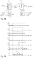
- FIG. 13 uses a block diagram to illustrate a further exemplary embodiment of a coding circuit which can be used in a bus interface circuit according to FIG. 4 , wherein the states of the low-priority data streams are stored in a register and the content of the register is transmitted, together with the state of the higher-priority data stream, in a frame via the coreless transformer.
- FIG. 3 is a diagram for illustrating the transmission paths used in a bus interface circuit, wherein a plurality of data streams are transmitted via the same galvanically isolating component.
- FIGS. 14-16 use exemplary timing diagrams to illustrate a further scheme for simultaneously transmitting two or more data streams via a coreless transformer, wherein the states of a plurality of data streams are combined in a frame.
- FIG. 17 illustrates examples of the implementation of different symbols for transmitting information via a coreless transformer.
- FIG. 18 uses exemplary timing diagrams to illustrate the interruption in a frame transmission and the start of a new frame transmission, wherein incomplete symbols are avoided by introducing a deterministic delay.
- FIG. 19 illustrates an exemplary implementation of the example from FIG. 13 in more detail.
- bus interface circuits for CAN bus systems relate to bus interface circuits for CAN bus systems. It goes without saying that the concepts described here can also be easily applied to other bus systems, for example LIN, Flexray or Profibus (Process Field Bus). The following description is therefore not restricted to CAN bus systems. It is also noted that the concepts described here can be used not only in the automotive sector but also in other industrial applications.
- FIG. 1 illustrates a general example of a bus node having a microcontroller 10 and a bus interface circuit 20 (bus interface for short) for a CAN bus (bus lines 30 ).
- the microcontroller 10 processes both the data to be transmitted via the bus and the data received by the bus, wherein the data are transmitted as serial data streams having a format corresponding to the bus protocol (for example CAN-FD protocol according to ISO 11898-1:2015).
- the data stream to be transmitted via the bus is referred to as the uplink data stream ULDAT 1 and the data stream received by the bus is referred to as the downlink data stream DLDAT 1
- the downlink data stream DLDAT 2 comes from another data source and was not received via the bus lines 30 .
- the data stream DLDAT 2 may contain, for example, status and diagnostic information (for example undervoltage warning) which can be produced by circuits contained in the bus interface 20 .
- the uplink data stream may contain, for example, status and diagnostic information which can be provided by the microcontroller 10 (or other sources), for example, and is intended to be transmitted to the other voltage domain.
- a further data stream ULDAT 2 or DLDAT 2 is transmitted only in the uplink or downlink path and only a single data stream (ULDAT 1 or DLDAT 1 ) is transmitted in the other direction.
- the bus interface 20 contains galvanic isolation 21 which is also sometimes referred to as a galvanic isolation barrier.
- the bus interface 20 is designed to receive the data stream ULDAT 1 via an external contact (for example TX pin), to transmit this data stream ULDAT 1 via the isolation barrier 21 and to convert it into a corresponding bus signal.
- this bus signal is a differential voltage signal which is provided at the external contacts (pins) CANE and CANT
- the contacts CANH and CANL are connected to the bus lines 30 (for example a twisted-pair cable).
- a data stream received by the bus is transmitted via the isolation barrier 21 and is made available to the microcontroller 10 at an external contact (for example RX pin) as a downlink data stream DLDAT 1 .
- Status and diagnostic information which is generated (in the figure) to the right of the isolation barrier 21 can also be transmitted via the isolation barrier 21 as a data stream/digital signal DLDAT 2 and can be made available to the microcontroller 10 at a further external contact (for example UV pin).
- status and diagnostic information can also be transmitted in the other direction (from the 48 V domain to the 12 V domain in the example illustrated) as a data stream/digital signal ULDAT 2 .
- the bus interface 20 can also be used as an interface between two supply voltage domains.
- all components to the right of the isolation barrier 21 are supplied via a 12 V voltage supply and all components to the left of the isolation barrier 21 are supplied via a 48 V voltage supply.
- Information is transmitted solely via the isolation barrier 21 .
- the latter may have a separate galvanically isolating component (for example a coreless transformer) for each data stream to be transmitted.
- the isolation barrier 21 comprises, for example, three coreless transformers for transmitting the data streams ULDAT 1 , DLDAT 1 and DLDAT 2 .
- FIG. 2 is a diagram for functionally illustrating an example of the transmission of data via the isolation barrier 21 within an integrated bus interface circuit 20 , wherein only the downlink data streams are illustrated. The situation is the same for uplink data streams and only the direction of the data transmission is reversed.
- two downlink data streams are transmitted in the interface circuit, a first data stream DLDAT 1 , which has a high priority, and a second data stream DLDAT 2 , which has a low priority.
- the high-priority data stream DLDAT 1 contains those data which have been received by the bus.
- This data stream DLDAT 1 has a format according to the bus protocol used, wherein comparatively high requirements with respect to jitter have to be met.
- the low-priority data stream DLDAT 2 may contain status and diagnostic data.
- the data streams DLDAT 1 and DLDAT 2 are asynchronous and are transmitted via separate galvanically isolating components in known bus interface circuits. If the isolation barrier 21 is implemented by means of coreless transformers, such a bus interface circuit comprises at least two coreless transformers for the high-priority uplink and downlink data streams and an additional coreless transformer for each further (uplink or downlink) data stream to be transmitted. In the case illustrated in FIG. 1 , this would be three coreless transformers.
- FIG. 3 is a diagram for functionally illustrating a further example of the transmission of data via the isolation barrier 21 within an integrated bus interface circuit 20 .
- the two data streams DLDAT 1 and DLDAT 2 are transmitted using the same galvanically isolating component.
- the data streams to be transmitted are coded and transmitted together (as one data stream).
- the data stream is decoded on the other side of the isolation barrier 21 , as a result of which the two data streams DLDAT 1 and DLDAT 2 are reconstructed again. If this approach is used, only a single coreless transformer is respectively required for the downlink data streams and the uplink data streams for transmitting the data.
- FIG. 4 is a block diagram of a first exemplary embodiment of a bus interface circuit for a CAN bus, wherein two or more uplink or downlink data streams are transmitted via the same coreless transformers.
- the example illustrated in FIG. 4 comprises an interface circuit 201 (physical CAN interface, CAN-PHY) which is connected to the external contacts CANH and CANL and is designed to convert a bus signal received at the external contacts CANH and CANL into a corresponding downlink data stream DLDAT 1 .
- the interface circuit 201 is also designed to receive an uplink data stream ULDAT 1 ′ and to convert it into a corresponding bus signal which is made available at the external contacts CANH and CANL.
- the interface circuit 201 substantially forms the physical layer within the Open Systems Interconnection (OSI) model (therefore the abbreviation CAN PHY).
- OSI Open Systems Interconnection
- the example illustrated in FIG. 4 also comprises coding circuits 202 and 204 .
- the coding circuit 202 is designed to receive the downlink data stream DLDAT 1 generated by the interface circuit 201 and at least one further downlink data stream DLDAT 2 and to combine the received data streams in one downlink data stream using special coding.
- the coding circuit 204 is designed, as it were, to receive the uplink data stream ULDAT 1 supplied at the external contact TX and at least one further uplink data stream ULDAT 2 and to combine the received data streams in one uplink data stream using special coding.
- the bus interface 20 also comprises an isolation barrier 21 having the coreless transformers 211 and 212 , wherein the coreless transformer 211 transmits the coded downlink data stream and the coreless transformer 212 transmits the coded uplink data stream.
- the uplink and downlink data streams transmitted via the isolation barrier 21 are supplied to the decoding circuits 203 and 205 .
- the decoding circuit 203 is designed to decode the downlink data stream transmitted via the isolation barrier 21 and to reconstruct the downlink data streams DLDAT 1 and DLDAT 2 again.
- the reconstructed downlink data streams are denoted DLDAT 1 ′ and DLDAT 2 ′.
- the reconstructed downlink data stream DLDAT 1 ′ is provided at the external contact RX.
- the decoding circuit 205 is designed to decode the uplink data stream transmitted via the isolation barrier 21 and to reconstruct the uplink data streams ULDAT 1 and ULDAT 2 again.
- the reconstructed uplink data streams are denoted ULDAT 1 ′ and ULDAT 2 ′.
- the reconstructed uplink data stream ULDAT 1 ′ is supplied to the interface circuit 201 (CAN PHY).
- the low-priority data streams ULDAT 2 and DLDAT 2 can be generated “on-chip”.
- the source of the data stream DLDAT 2 may be a circuit which is contained in the bus interface 20 , for example a circuit which generates diagnostic and status signals relating to the physical CAN interface 201 .
- the data stream ULDAT 2 can be received via an external pin of the bus interface 20 and can be supplied to the coding circuit 204 . This may be useful, for example, when low-priority data or signals are intended to be transmitted from one voltage domain (for example 48 V) to another voltage domain (for example 12 V).
- a low-priority data stream ULDAT 2 supplied via an external pin can be generated by the microcontroller 10 , for example (cf. FIG. 1 ).
- the source of the further data streams ULDAT 2 and DLDAT 2 is irrelevant for the use of the concepts described here.
- the data streams ULDAT 1 and DLDAT 1 contain the data to be transmitted via the bus in a format corresponding to the bus protocol. These data streams therefore have a comparatively high priority.
- the coding circuits 202 and 204 can therefore transmit the data streams ULDAT 1 and DLDAT 1 with preference over (that is to say with higher priority than) the further data streams ULDAT 2 and DLDAT 2 via the coreless transformers 211 and 212 in order to keep the latencies and the jitter low in the data streams ULDAT 1 and DLDAT 1 .
- coding two asynchronous data streams for example downlink data streams DLDAT 1 and DLDAT 2
- DLDAT 1 and DLDAT 2 downlink data streams
- DLDAT 2 downlink data streams
- the coding circuits 202 , 204 autonomously determine the time slots for transmitting the coded data streams.
- a first symbol is transmitted via the coreless transformer if the state of the data stream ULDAT 1 changes from dominant to recessive and a second symbol is transmitted if the state of the data stream ULDAT 1 changes from recessive to dominant.
- Other symbols are used for coding the data stream ULDAT 2 . The symbols are combined to form a symbol sequence and this symbol sequence is transmitted via the coreless transformer.
- the transmission via a coreless transformer using different symbols is known per se and is therefore not explained any further.
- the approaches described here can ensure that no conflicts occur during the transmission of two data streams if symbols are transmitted via the coreless transformer.
- the symbol sequence is constructed in the coding circuits 202 , 204 in such a manner that the symbols assigned to the edges of the high-priority data stream ULDAT 1 or DLDAT 1 are always delayed by the same value (which may also be approximately zero) relative to the associated edges in order to avoid jitter in the high-priority data stream.
- the transmission of the symbols assigned to the edges or logic levels of the low-priority data stream ULDAT 2 or DLDAT 2 is delayed in the event of an imminent collision (that is to say if two symbols would have to be transmitted at the same time without delay), as a result of which jitter is indeed produced, but is not critical in low-priority data streams.
- the high-priority data stream (for example downlink data stream DLDAT 1 ) is formatted according to a bus protocol.
- deterministic gaps in the data transmission which are stipulated in the bus protocol are used to transmit the lower-priority data stream (for example downlink data stream DLDAT 2 ) via the coreless transformer. Suitable gaps can be detected by a protocol handler PH and can be signaled to the respective coding circuit 202 or 204 .
- the protocol handler can be implemented in the microcontroller (see FIG. 1 ) which also generates the uplink data stream.
- a protocol handler may also be implemented in the bus interface 20 .
- a protocol handler may likewise be integrated in the bus interface 20 and may be coupled to the bus transceiver 210 .
- a protocol handler PH is not necessary in all exemplary embodiments and is therefore optional.
- the bus protocol provides a pause between two frames which corresponds to the length of ten bits, seven bits of which are recessive bits of the end-of-frame (EOF) field and three of which are recessive bits of the intermission-frame-space (IFS) field.
- EEF end-of-frame
- IFS intermission-frame-space
- FIG. 5 illustrates the end of a CAN frame of the data stream ULDAT 1 .
- the last bit of the data transmission is effected in the first bit of the so-called acknowledge (ACK) field which is followed by a recessive bit (ACK delimiter bit).
- ACK acknowledge
- ACK delimiter bit a recessive bit
- the transmission of the lower-priority data stream ULDAT 2 can start, for example via the coreless transformer 211 (see FIG. 4 ) (see lower diagram in FIG. 5 ).
- This data transmission should be concluded by the end of the IFS field.
- the data stream ULDAT 2 is transmitted in a time slot having the length of 9 bits of the data stream ULDAT 1 .
- a further deterministic gap can be produced after the arbitration field of a CAN frame.
- a bus node that is to say the protocol handler decides whether data continue to be transmitted or whether the transmission is stopped. If the transmission is stopped, the protocol handler “knows” that no data are transmitted to the bus until the next acknowledge delimiter bit is received.
- This gap can also be used to transmit the lower-priority data stream via the coreless transformer 212 .
- this approach functions only for uplink data streams and presupposes that the bus communication is active. If the bus is inactive, low-priority data streams cannot be transmitted either because the inactivity period is not guaranteed.
- the data streams are transmitted via a coreless transformer in an interleaved manner.
- FIG. 6 The first (upper) timing diagram shows an example of a data stream DLDAT 1 which was received by the CAN transceiver (see FIG. 4 ).
- the clock signal of the transmitter is recovered (clock recovery) on the basis of this data stream, wherein, in the example illustrated, the clock signal CLK R is synchronized with the falling edges in the data stream DLDAT 1 (see FIG. 6 , second diagram).
- a period of the clock signal corresponds to the duration of one bit in the data stream DLDAT 1 .
- the low-priority data stream DLDAT 2 is asynchronous with respect to the data stream DLDAT 1 (see FIG. 6 , third diagram). However, the data stream DLDAT 2 is synchronized by sampling it approximately in the middle of a bit period of the data stream DLDAT 1 . In the example illustrated, the low-priority data stream DLDAT 2 is sampled in sync with the rising edges of the regenerated clock signal CLK R . The sampled/synchronized low-priority data signal is denoted DLDAT 2 * (see FIG. 6 , fourth diagram).
- the edges of the data stream DLDAT 1 are coded with a positive current pulse (first symbol) and the edges of the data stream DLDAT 2 * are coded with a negative current pulse (second symbol). Since the edges of the synchronized data stream DLDAT 2 * are always in the middle of a bit period of the data stream DLDAT 1 , no collisions can occur during transmission via the coreless transformer (cf. FIG. 4 , coreless transformer 211 ).
- the current pulses (also called symbols) transmitted via the coreless transformer are illustrated in the lowermost diagram.
- the current flowing through the primary side of the coreless transformer is denoted i CT .
- edges of the signals DLDAT 1 and DLDAT 2 * are likewise distinguished by the use of different symbols. Examples of different symbols are also explained below (cf. also FIG. 11 ).
- the approach described with respect to FIG. 6 can be used to transmit both uplink data streams and downlink data streams.
- the clock signal need not be recovered from the data stream ULDAT 1 since it can be provided by the protocol handler anyway.
- it is necessary to regenerate the clock signal.
- transmission of low-priority data streams may be problematic if the bus communication is inactive because the inactivity period is not guaranteed.
- a further approach which allows the transmission of a first high-priority data stream (for example data stream DLDAT 1 ) and at least one further low-priority data stream DLDAT 2 via the same coreless transformer (cf. FIG. 4 , reference sign 211 ) is explained on the basis of the timing diagrams in FIGS. 7 to 9 .
- the temporal length T S of a symbol which is transmitted via the coreless transformer and represents an edge of a digital signal is only a fraction (approximately 10%) of the length of a bit of the high-priority data stream.
- the transmission of the edges of the high-priority data stream DLDAT 1 is delayed by a period corresponding to the symbol length T S .
- the associated symbol is transmitted a time T S later via the coreless transformer.
- This transmission is consequently concluded a time 2T S after the detected edge.
- the coreless transformer is therefore used for a period 2T S after a detected edge of the high-priority data stream DLDAT 1 and cannot be used to transmit other edges.
- FIG. 7 uses timing diagrams to illustrate a first of the data transmission, wherein an edge in the low-priority data stream DLDAT 2 occurs more than 2T S after an edge in the high-priority data stream DLDAT 1 .
- the first diagram (from the top) in FIG. 7 shows a rising edge of the data stream DLDAT 1 .
- a detected edge is indicated by a signal EDOUT, the logic level of which is set to “high” for a period 2T S in response to a detected edge in the data stream DLDAT 1 . That is to say, each detected edge triggers, in the signal EDOUT, a pulse whose length corresponds to twice the symbol length 2T S .
- This signal EDOUT is illustrated in the second diagram in FIG.
- the symbol representing the edge of the data stream DLDAT 1 is denoted S 1 in FIG. 4 (see FIG. 7 , fourth diagram).
- the subsequently occurring edge in the data stream DLDAT 2 is represented by the symbol S 2 which is transmitted without delay in the case illustrated.
- FIG. 8 illustrates a second case in which an edge of the lower-priority data stream DLDAT 2 occurs shortly after an edge of the high-priority data stream DLDAT 1 .
- “shortly after” means that the edge of the data stream DLDAT 2 occurs less than a time 2T S after an edge of the data stream DLDAT 1 , that is to say while the transmission channel is still being used (indicated by the signal EDOUT, see FIG. 8 , first, second and third diagrams).
- the transmission of the edge of the low-priority data stream DLDAT 2 is delayed by at least a time 2T S (see FIG. 8 , fifth diagram, symbol S 2 ).
- the delayed signal is denoted DLDAT 2 * (see FIG.
- the edge of the high-priority signal DLDAT 1 is again transmitted with a delay of T S (see FIG. 8 , fifth diagram, symbol S 1 ).
- the delay in the transmission of the symbol S 2 causes jitter in the low-priority data stream DLDAT 2 . This jitter is acceptable for most applications.
- the delay in the transmission of the symbol S 1 does not cause jitter in the high-priority data stream DLDAT 1 since this delay is the same for each edge.
- FIG. 9 illustrates a third case in which an edge of the lower-priority data stream DLDAT 2 occurs shortly before an edge of the high-priority data stream DLDAT 1 (see FIG. 9 , first and third diagrams).
- the example illustrated in FIG. 9 shows the advantage of the constant delay of the high-priority data stream DLDAT 1 by a symbol length T S .
- the edge in the data stream DLDAT 2 occurs at a time at which the transmission channel is not yet being used and the symbol S 2 is transmitted substantially without delay (see FIG. 9 , fourth diagram).
- the transmission of the symbol S 2 lasts for a maximum time T S and therefore cannot collide with the—always delayed—transmission of the symbol S 1 .
- the symbol S 2 will be only in the first half of the pulse in the signal EDOUT, whereas the symbol S 1 is always transmitted in the second half of the pulse in the signal EDOUT (see FIG. 9 , second and fourth diagrams).
- the introduction of a deterministic delay in the transmission of the high-priority data stream DLDAT 1 does not cause any jitter (since this delay is introduced for each individual edge) but makes it possible to avoid a collision if another symbol is already being transmitted when an edge of the data stream DLDAT 1 is detected.
- the jitter produced by the delay in the transmission of an edge of the data stream DLDAT 2 (cf. FIG. 8 ) is accepted and is not critical for most applications.
- the fifth diagram from FIG. 9 is explained further below together with FIG. 10 .
- FIG. 10 is a block diagram which shows an exemplary implementation of the coding circuit 202 in order to implement the approach illustrated in FIGS. 7-9 .
- the coding circuit 202 is in the downlink path; the coding circuit 204 in the uplink path can be implemented in the same manner.
- the coding circuit 202 has an edge detection circuit 52 which is supplied with the high-priority data stream DLDAT 1 and is designed to detect the edges contained in the data stream DLDAT 1 . For each detected edge, a pulse of the length 2T S is output at the output of the edge detection circuit 52 .
- the output signal is denoted EDOUT.
- the edge detection circuit 52 can substantially contain an edge-triggered monostable multivibrator (monoflop) which generates a pulse of the length 2T S as an output signal for each rising and falling edge.
- the coding circuit 202 has a delay element 51 which is designed to delay the data stream DLDAT 1 by a time T S .
- the delayed data stream DLDAT 1 * is supplied to the coding unit 53 which is designed to code the edges of the data stream DLDAT 1 * as symbols (cf. FIG. 7 , symbol S 1 ).
- the low-priority data stream DLDAT 2 is supplied to the delay element 54 which is designed not to delay the clock edges of the data stream DLDAT 2 if the edge detection circuit 52 does not indicate a detected edge (EDOUT is at a logic 0 level) and to delay the clock edges of the data stream DLDAT 2 by a period 2T S (or more) if the edge detection circuit 52 indicates a detected edge (EDOUT is at a logic 1 level).
- the (partially) delayed signal DLDAT 2 * is supplied to the coding unit 55 which is designed to code the edges of the data stream DLDAT 2 * as symbols (cf. FIG. 7 , symbol S 2 ).
- the outputs of the coding units 53 and 55 are supplied to a multiplexer 56 which is designed to connect either the output of the coding unit 53 (assigned to the data stream DLDAT 1 ) or the output of the coding unit 55 (assigned to the data stream DLDAT 2 ) to the input of the driver circuit 57 which converts symbols generated by the coding units 53 and 55 into corresponding current signals i CT for the coreless transformer.
- the coding circuit 53 for example, can generate a control signal MSW (cf. FIG. 9 , lowermost diagram) which causes the multiplexer 56 to switch through the coded output signal from the coding circuit 53 to the TX driver 57 if a symbol is currently intended to be transmitted. Otherwise, the output of the coding circuit 55 is switched through to the TX driver 57 .
- FIG. 11 illustrates the function of the coding circuit 202 from FIG. 10 using exemplary timing diagrams.
- the first half of the timing diagrams from FIG. 11 shows substantially the same situation as in FIG. 7 .
- the signal EDOUT from the edge detection circuit 52 exhibits a pulse of the length 2T S immediately following an edge (rising and falling) in the high-priority data stream DLDAT 1 (see FIG. 11 , first and second diagrams).
- the associated symbols S 1 and S 1 ′ are transmitted precisely a time T S after the respective edge, wherein the symbol S 1 represents a rising edge and the symbol S 1 ′ represents a falling edge (see FIG. 11 , first and third diagrams).
- edges of the low-priority data stream DLDAT 2 are not transmitted with a delay (immediately) (symbols S 2 and S 2 ′ for rising and falling edges) since the edge does not fall in the period which is indicated by the signal EDOUT and in which the coreless transformer is reserved for the transmission of the high-priority data stream DLDAT 1 .
- a symbol is represented by two short current pulses.
- FIG. 12 uses timing diagrams to show how the current pulses (symbols) transmitted via the coreless transformer are decoded again.
- the reconstructed data streams are denoted DLDAT 1 ′ and DLDAT 2 ′.
- the decoding circuit see FIG. 4 , reference sign 203 ) has received a symbol, the level at the first or second output, at which the first data stream DLDAT 1 ′ or the second data stream DLDAT 2 ′ is output, is changed depending on the received symbol.
- the level at the first output (data stream DLDAT 1 ′) is set to “high”; if a symbol S 2 is received, the level at the second output (data stream DLDAT 2 ′) is set to “high”; if a symbol S 1 ′ is received, the level at the first output (data stream DLDAT 1 ′) is set to “low” again; and, if a symbol S 2 ′ is received, the level at the second output (data stream DLDAT 2 ′) is set to “low” again.
- the original high-priority data stream DLDAT 1 is illustrated using dashed lines in the central diagram in FIG. 12 . It is seen that the reconstructed data stream DLDAT 1 ′ has been delayed by a time 2T S . However, this delay is deterministic and does not cause any jitter.
- the alternative approach described below makes it possible to transmit a plurality of low-priority signals DLDAT 2 , DLDAT 3 , DLDAT 4 together with a high-priority signal DLDAT 1 via a coreless transformer.
- edges of the high-priority signal DLDAT 1 are transmitted without a significant delay or—alternatively—always with the same constant delay (in a similar manner to the examples from FIGS. 7-9 ) in order to avoid generating jitter.
- the logic values of the low-priority signals DLDAT 2 , DLDAT 3 , DLDAT 4 are combined in one data frame and are transmitted together with the edge of the high-priority signal DLDAT 1 .
- the frame is regularly transmitted, for example if one of the logic levels of the signals DLDAT 2 , DLDAT 3 , DLDAT 4 changes and/or if a particular period has elapsed.
- a collision may potentially occur if, during the transmission of a frame, an edge occurs in the high-priority signal DLDAT 1 .
- the following examples are used to explain how such a conflict can be resolved.
- FIG. 13 is a simplified block diagram of an exemplary implementation of a bus interface circuit 2 similar to FIG. 4 .
- the uplink path may have substantially the same structure (cf. FIG. 4 ).
- the illustrated example is substantially the same as the example from FIG. 4 , wherein registers 61 , 62 which can store the logic levels of the low-priority signals DLDAT 2 , DLDAT 3 , DLDAT 4 are additionally provided.
- the coding circuit 202 reads the content of the register 61 and composes the information contained therein to form a frame.
- the decoding circuit 203 receives the symbols received via the coreless transformer 211 and reconstructs the high-priority signal DLDAT 1 ′ and the low-priority signals DLDAT 2 , DLDAT 3 , DLDAT 4 , wherein the binary values of the signals DLDAT 2 , DLDAT 3 , DLDAT 4 are written to the register 62 .
- the reconstructed signals DLDAT 2 ′, DLDAT 3 ′, DLDAT 4 ′ can be tapped off at the output of the register 62 .
- the registers 61 and 62 may be implemented as shift registers, for example.
- FIG. 14 contains exemplary timing diagrams of the high-priority signal DLDAT 1 , the sampling signal SMP which blocks updating of the content of the register 61 during the transmission of a frame, the low-priority signals DLDAT 2 , DLDAT 3 , DLDAT 4 , the register content REG DAT of the register 61 and the symbols transmitted via the coreless transformer (signal i CT ).
- the transmission of a frame is triggered by the detection of an edge in the high-priority signal DLDAT 1 . In the present example, the transmission is carried out virtually without a significant delay.
- the signal SMP exhibits a pulse of the length T F which corresponds substantially to the temporal length of a frame. During this time T F , updating of the register 61 is blocked in order to keep the register content consistent.
- the content of the register is initially “100” (high level of the signal DLDAT 2 , low level of the signal DLDAT 3 and low level of the signal DLDAT 4 ) and subsequently changes to “101” (high level of the signal DLDAT 2 , low level of the signal DLDAT 3 and high level of the signal DLDAT 4 ).
- the signal DLDAT 4 changes from “0” to “1” already at the time t x , but the register 61 is updated only thereafter, after the transmission of the frame has been concluded (that is to say with the falling edge of the signal SMP).
- the transmission of the frame is triggered by the detection of an edge in the signal DLDAT 1 and begins without a significant delay in the present example.
- a frame begins with a start symbol SOF (Start of Frame) and ends with a closing symbol EOF (End of Frame). 0 symbols and 1 symbols are transmitted according to the content of the register 61 between the symbols SOF and EOF.
- FIG. 15 illustrates, as a further example, a situation in which the content of the register 61 (that is to say one of the low-priority signals DLDAT 2 , DLDAT 3 , DLDAT 4 ) changes in a phase in which no communication is taking place on the CAN bus.
- the first transmission of a frame illustrated in FIG. 15 (lower diagram) is triggered by a rising edge in the high-priority signal DLDAT 1 .
- the second transmission of a frame is triggered by a falling edge in the high-priority signal DLDAT 1 .
- the start symbols SOF 1 and SOF 2 which in this case respectively represent a rising and a falling edge of the signal DLDAT 1 .
- the content of the register 61 changes at the time t y . Since no communication is taking place on the CAN bus at this time, the transmission of a frame is triggered in this situation by the change in the content of the register 61 .
- the third transmission of a frame illustrated in FIG. 15 again begins with the start symbol SOF 2 for a falling edge. Since the state of the signal DLDAT 1 is already a low level, the signal DLDAT 1 is not influenced by the third frame transmission, but rather only the register content is transmitted. Additionally or alternatively, further frames can be transmitted at predefined intervals of time as long as no communication is taking place on the CAN bus.
- the transmission of the first frame is triggered by a rising edge in the signal DLDAT 1
- the frame begins with the start symbol SOF 1 which indicates a rising edge.
- the content of the register 61 subsequently changes without communication taking place on the bus.
- the transmission of the second frame is therefore triggered by the change in the register content.
- a falling edge is detected in the high-priority signal DLDAT 1 and the frame transmission must be aborted.
- the frame abort is signaled by the signal FSTOP (short pulse at the time t z ) which is triggered by the detected falling edge.
- the incompletely transmitted frame is identified by virtue of the fact that a start symbol (symbol SOF 2 in the example illustrated) is received without a closing symbol EOF having been received beforehand.
- the incompletely received frame is discarded in the decoder.
- FIG. 17 illustrates examples of the data symbols (0 symbol and 1 symbol) and the start symbols SOF 1 and SOF 2 which represent rising and falling edges.
- FIG. 17 contains four diagrams, wherein (from left to right) a 0 symbol, a 1 symbol, a start symbol SOF 1 for rising edges and a start symbol SOF 2 for falling edges are respectively illustrated.
- the closing symbols EOF 1 , EOF 2 can be the same as the associated start symbols SOF 1 and SOF 2 .
- the data symbols are formed by long current pulses, whereas the start symbols are formed by short current pulses. In all cases, the symbol length is always T S .
- the start symbol SOF 2 is produced in the event of a premature abort of the 0 symbol at the time t A (for example the time of a detected falling edge in the high-priority signal).
- this start symbol which is incorrectly identified in the decoder as SOF 2 begins a time T J before the time t A , which results in corresponding jitter.
- a deterministic delay (dead time, latency) of one symbol length T S can be introduced—in a similar manner to that in the examples according to FIGS. 7-9 .
- an (already started) transmission of a symbol can therefore always be concluded before the transmission of a new frame begins.
- An example of this approach is illustrated in FIG. 18 .
- the first two timing diagrams (from the top) from FIG. 18 show the high-priority data stream DLDAT 1 with a falling edge at the time t A and the data stream DLDAT 1 * delayed by a symbol length T S .
- the edge occurs at the time t A while a frame is currently being transmitted via the cureless transformer (see third diagram from FIG. 18 ).
- An immediate abort of the frame transmission at the time t A would abort the transmission of the 0 symbol after approximately the first third of the symbol, which would cause a situation like in the first diagram in FIG. 17 (early start symbol causes jitter).
- the current transmission of a symbol can be correctly completed in the event of a frame abort before the transmission of the new frame begins.
- This approach causes unproblematic additional latency, which corresponds to the delay T S , but does not cause any jitter.
- the frame abort is indicated by a pulse in the signal FSTOP (fourth diagram in FIG. 18 ).
- FIG. 19 illustrates an exemplary implementation of the coding circuit 202 from FIG. 13 in more detail.
- the coding circuit 202 comprises a frame composition unit 63 which receives the high-priority data stream DLDAT 1 , the content REG DAT of the register 6 and a trigger signal TRIG.
- the frame composition unit 63 can be designed to compose a frame representing the current state of the high-priority data stream DLDAT 1 and the register content REG DAT in response to the trigger signal TRIG.
- a frame is initially only a sequence of symbols which is supplied to the coding unit 53 .
- the coding unit 53 is designed to convert the symbols into an accordingly modulated driver signal (cf., for example, FIG. 17 ).
- the driver 57 is connected downstream of the coding unit 53 and, in accordance with the driver signal, generates a modulated current i CT which is supplied to the primary side of the coreless transformer and is transmitted the coreless transformer.
- the transmission of a frame is triggered by the trigger signal TRIG.
- the trigger signal TRIG is an OR combination (by means of OR gate 66 ) of the output signals from an edge detection unit 52 , a timer 64 and a circuit 65 which indicates a change in the content of the register 61 (see FIG. 13 ).
- the transmission of a frame is therefore triggered the following events: (a) an edge is detected in the high-priority signal DLDAT 1 , (b) the content of the register 61 has changed and (c) a defined time has elapsed since the last transmission (indicated by timer 64 ). If—as in the example from FIG.
- a deterministic delay is intended to be introduced between an edge in the data stream DLDAT 1 and the transmission of a frame, the delay can be achieved by means of a delay element 51 between the edge detection unit 52 and the OR gate 66 .
- a frame abort is signaled by the signal FSTOP which is generated by the edge detection unit 52 when an edge is detected and is supplied to the coding circuit 53 .
- the coding circuits 202 and 204 can be implemented in many different ways. The implementations shown in FIGS. 4, 10, 13 and 18 should be understood merely as examples, and it goes without saying that a person skilled in the art will find various other implementations which perform substantially the same function which has been explained in detail in connection with the timing diagrams illustrated in the figures.
- the coding circuits 202 and 204 and the decoding circuits 203 and 205 can be implemented by means of known digital circuit components and programmable circuits (for example programmable logic circuits). In some exemplary embodiments, at least some components of the coding circuits and/or decoding circuits can be implemented by means of a processor and suitable firmware.
- the examples described here relate to the transmission of data streams via a coreless transformer in the downlink path (that is to say to the microcontroller, cf. FIG. 1 ). Even if not explicitly illustrated, data streams are transmitted in the uplink path (that is to say from the microcontroller, cf. FIG. 1 ) in a similar manner. It goes without saying that other galvanically isolating components, for example optocouplers, capacitive components, etc., can also be used instead of coreless transformers in the exemplary embodiments described here. It is also noted that the implementations illustrated in FIGS. 4, 10, 13 and 19 should be understood merely as examples, and a person skilled in the art is able to easily find other or modified implementations which perform substantially the same function.
Abstract
Description
Claims (21)
Applications Claiming Priority (3)
| Application Number | Priority Date | Filing Date | Title |
|---|---|---|---|
| DE102018106085 | 2018-03-15 | ||
| DE102018106085.8A DE102018106085B3 (en) | 2018-03-15 | 2018-03-15 | interface circuit |
| DE102018106085.8 | 2018-03-15 |
Publications (2)
| Publication Number | Publication Date |
|---|---|
| US20190288886A1 US20190288886A1 (en) | 2019-09-19 |
| US10728064B2 true US10728064B2 (en) | 2020-07-28 |
Family
ID=67224549
Family Applications (1)
| Application Number | Title | Priority Date | Filing Date |
|---|---|---|---|
| US16/296,042 Active US10728064B2 (en) | 2018-03-15 | 2019-03-07 | Interface circuit |
Country Status (3)
| Country | Link |
|---|---|
| US (1) | US10728064B2 (en) |
| CN (1) | CN110275853B (en) |
| DE (1) | DE102018106085B3 (en) |
Families Citing this family (1)
| Publication number | Priority date | Publication date | Assignee | Title |
|---|---|---|---|---|
| US10778481B1 (en) * | 2019-03-25 | 2020-09-15 | Delphi Technologies Ip Limited | Adaptable can transceiver and system |
Citations (3)
| Publication number | Priority date | Publication date | Assignee | Title |
|---|---|---|---|---|
| US20110026612A1 (en) * | 2009-07-31 | 2011-02-03 | Stmicroelectronics S.R.L. | Receiver for signal communication apparatus and related signal communication apparatus |
| US20110289248A1 (en) | 2010-05-21 | 2011-11-24 | National Semiconductor Corporation | Isolated communication bus and related protocol |
| US20150229149A1 (en) * | 2014-02-13 | 2015-08-13 | Infineon Technologies Austria Ag | Switched Mode Power Supply Circuit |
Family Cites Families (6)
| Publication number | Priority date | Publication date | Assignee | Title |
|---|---|---|---|---|
| US6608574B1 (en) * | 2002-03-29 | 2003-08-19 | Siemens Energy & Automation, Inc. | Device, system, and method for compensating for isolation and cable delays in an SSI encoder interface circuit |
| US9322883B2 (en) * | 2012-04-09 | 2016-04-26 | Jabil Circuit, Inc. | Battery monitoring system using time-based signals |
| US8928383B2 (en) * | 2013-03-15 | 2015-01-06 | Analog Devices, Inc. | Integrated delayed clock for high speed isolated SPI communication |
| JP2014232954A (en) * | 2013-05-28 | 2014-12-11 | オリンパスメディカルシステムズ株式会社 | Digital data transmitter |
| US9531280B2 (en) * | 2014-05-09 | 2016-12-27 | Avago Technologies General Ip (Singapore) Pte. Ltd. | Isolation device and system |
| JP2017147538A (en) * | 2016-02-16 | 2017-08-24 | 三菱電機株式会社 | Isolator and isolation method |
-
2018
- 2018-03-15 DE DE102018106085.8A patent/DE102018106085B3/en active Active
-
2019
- 2019-03-07 US US16/296,042 patent/US10728064B2/en active Active
- 2019-03-15 CN CN201910199969.9A patent/CN110275853B/en active Active
Patent Citations (3)
| Publication number | Priority date | Publication date | Assignee | Title |
|---|---|---|---|---|
| US20110026612A1 (en) * | 2009-07-31 | 2011-02-03 | Stmicroelectronics S.R.L. | Receiver for signal communication apparatus and related signal communication apparatus |
| US20110289248A1 (en) | 2010-05-21 | 2011-11-24 | National Semiconductor Corporation | Isolated communication bus and related protocol |
| US20150229149A1 (en) * | 2014-02-13 | 2015-08-13 | Infineon Technologies Austria Ag | Switched Mode Power Supply Circuit |
Non-Patent Citations (1)
| Title |
|---|
| Office Action, in the German language, from counterpart German Application No. 102018106085.8, dated Jan. 10, 2019, 4 pp. |
Also Published As
| Publication number | Publication date |
|---|---|
| DE102018106085B3 (en) | 2019-08-01 |
| US20190288886A1 (en) | 2019-09-19 |
| CN110275853A (en) | 2019-09-24 |
| CN110275853B (en) | 2023-11-03 |
Similar Documents
| Publication | Publication Date | Title |
|---|---|---|
| KR101885935B1 (en) | Method and apparatus for serial data transmission at a switchable data rate | |
| Di Natale et al. | Understanding and using the controller area network communication protocol: theory and practice | |
| US9252969B2 (en) | Method for transmitting data | |
| RU2597502C2 (en) | Method and device for memory size adapted serial data transfer | |
| US9461937B2 (en) | Method and device for a serial data transmission with additionally inserted data | |
| JP6324618B2 (en) | Method for serially transmitting a frame from a transmitting side to at least one receiving side and a subscriber station of the bus system via a bus system | |
| CN106464559B (en) | High speed embedded protocol for distributed control system | |
| US20140298133A1 (en) | Method and device for serially transferring data, having switchable data encoding | |
| RU2562363C2 (en) | Method of controlling access to transmission medium for busbar and communication device | |
| WO2016054245A1 (en) | Confirming data accuracy in a distributed control system | |
| US20160224501A1 (en) | Adaptation device for a bus system, and method for operating a can subscriber station and a can fd subscriber station in a bus system | |
| RU2678715C2 (en) | Data transmission protocol with protocol exception state | |
| EP3599743B1 (en) | Method and device for communicating data frames on a multi-master bus | |
| TW201322689A (en) | Method for operating a communications assembly | |
| CN112422295B (en) | Ethernet interface and related system, method and equipment | |
| KR20220012988A (en) | Error detection test apparatus for subscriber station of serial bus system and test method of error detection mechanism in communication in serial bus system | |
| EP2458772A2 (en) | Method and system for synchronizing a network using existing network cables | |
| EP2985955A1 (en) | Controller area network (can) device and method for emulating classic can error management | |
| US10728064B2 (en) | Interface circuit | |
| CN112823496B (en) | Frame masking unit, subscriber station for a serial bus system and method for communication in a serial bus system | |
| EP2940935B1 (en) | Controller area network (CAN) device and method for controlling CAN traffic | |
| CN112859663A (en) | Fieldbus system with switchable slew rate | |
| CN113542082A (en) | Bus transceiver | |
| KR20230045061A (en) | Subscriber stations for serial bus systems and communication methods in serial bus systems |
Legal Events
| Date | Code | Title | Description |
|---|---|---|---|
| FEPP | Fee payment procedure |
Free format text: ENTITY STATUS SET TO UNDISCOUNTED (ORIGINAL EVENT CODE: BIG.); ENTITY STATUS OF PATENT OWNER: LARGE ENTITY |
|
| AS | Assignment |
Owner name: INFINEON TECHNOLOGIES AG, GERMANY Free format text: ASSIGNMENT OF ASSIGNORS INTEREST;ASSIGNORS:MANGST, MAXIMILIAN;PIHET, ERIC;HINDERER, THORSTEN;REEL/FRAME:048894/0446 Effective date: 20190327 |
|
| STPP | Information on status: patent application and granting procedure in general |
Free format text: DOCKETED NEW CASE - READY FOR EXAMINATION |
|
| STPP | Information on status: patent application and granting procedure in general |
Free format text: NON FINAL ACTION MAILED |
|
| STPP | Information on status: patent application and granting procedure in general |
Free format text: RESPONSE TO NON-FINAL OFFICE ACTION ENTERED AND FORWARDED TO EXAMINER |
|
| STPP | Information on status: patent application and granting procedure in general |
Free format text: NOTICE OF ALLOWANCE MAILED -- APPLICATION RECEIVED IN OFFICE OF PUBLICATIONS |
|
| STPP | Information on status: patent application and granting procedure in general |
Free format text: PUBLICATIONS -- ISSUE FEE PAYMENT RECEIVED |
|
| STPP | Information on status: patent application and granting procedure in general |
Free format text: PUBLICATIONS -- ISSUE FEE PAYMENT VERIFIED |
|
| STCF | Information on status: patent grant |
Free format text: PATENTED CASE |
|
| MAFP | Maintenance fee payment |
Free format text: PAYMENT OF MAINTENANCE FEE, 4TH YEAR, LARGE ENTITY (ORIGINAL EVENT CODE: M1551); ENTITY STATUS OF PATENT OWNER: LARGE ENTITY Year of fee payment: 4 |