WO2012131884A1 - マルチコアプロセッサシステム - Google Patents
マルチコアプロセッサシステム Download PDFInfo
- Publication number
- WO2012131884A1 WO2012131884A1 PCT/JP2011/057715 JP2011057715W WO2012131884A1 WO 2012131884 A1 WO2012131884 A1 WO 2012131884A1 JP 2011057715 W JP2011057715 W JP 2011057715W WO 2012131884 A1 WO2012131884 A1 WO 2012131884A1
- Authority
- WO
- WIPO (PCT)
- Prior art keywords
- application
- memory
- processor system
- core processor
- memory area
- Prior art date
Links
Images


Classifications
-
- G—PHYSICS
- G06—COMPUTING; CALCULATING OR COUNTING
- G06F—ELECTRIC DIGITAL DATA PROCESSING
- G06F12/00—Accessing, addressing or allocating within memory systems or architectures
- G06F12/14—Protection against unauthorised use of memory or access to memory
- G06F12/1458—Protection against unauthorised use of memory or access to memory by checking the subject access rights
- G06F12/1483—Protection against unauthorised use of memory or access to memory by checking the subject access rights using an access-table, e.g. matrix or list
-
- G—PHYSICS
- G06—COMPUTING; CALCULATING OR COUNTING
- G06F—ELECTRIC DIGITAL DATA PROCESSING
- G06F11/00—Error detection; Error correction; Monitoring
- G06F11/07—Responding to the occurrence of a fault, e.g. fault tolerance
- G06F11/16—Error detection or correction of the data by redundancy in hardware
- G06F11/1658—Data re-synchronization of a redundant component, or initial sync of replacement, additional or spare unit
-
- G—PHYSICS
- G06—COMPUTING; CALCULATING OR COUNTING
- G06F—ELECTRIC DIGITAL DATA PROCESSING
- G06F21/00—Security arrangements for protecting computers, components thereof, programs or data against unauthorised activity
- G06F21/70—Protecting specific internal or peripheral components, in which the protection of a component leads to protection of the entire computer
- G06F21/78—Protecting specific internal or peripheral components, in which the protection of a component leads to protection of the entire computer to assure secure storage of data
-
- G—PHYSICS
- G06—COMPUTING; CALCULATING OR COUNTING
- G06F—ELECTRIC DIGITAL DATA PROCESSING
- G06F11/00—Error detection; Error correction; Monitoring
- G06F11/07—Responding to the occurrence of a fault, e.g. fault tolerance
- G06F11/16—Error detection or correction of the data by redundancy in hardware
- G06F11/1666—Error detection or correction of the data by redundancy in hardware where the redundant component is memory or memory area
- G06F11/167—Error detection by comparing the memory output
-
- G—PHYSICS
- G06—COMPUTING; CALCULATING OR COUNTING
- G06F—ELECTRIC DIGITAL DATA PROCESSING
- G06F11/00—Error detection; Error correction; Monitoring
- G06F11/07—Responding to the occurrence of a fault, e.g. fault tolerance
- G06F11/16—Error detection or correction of the data by redundancy in hardware
- G06F11/20—Error detection or correction of the data by redundancy in hardware using active fault-masking, e.g. by switching out faulty elements or by switching in spare elements
-
- G—PHYSICS
- G06—COMPUTING; CALCULATING OR COUNTING
- G06F—ELECTRIC DIGITAL DATA PROCESSING
- G06F12/00—Accessing, addressing or allocating within memory systems or architectures
- G06F12/14—Protection against unauthorised use of memory or access to memory
- G06F12/1458—Protection against unauthorised use of memory or access to memory by checking the subject access rights
- G06F12/1491—Protection against unauthorised use of memory or access to memory by checking the subject access rights in a hierarchical protection system, e.g. privilege levels, memory rings
Definitions
- the present invention relates to a multi-core processor system that protects software.
- FIG. 10 is an explanatory diagram showing an operation example when the software for the single core processor system operates on the multi-core processor system.
- the explanatory diagram denoted by reference numeral 1001 describes the case where the application 1003 operates on a single core processor system
- the explanatory diagram denoted by reference numeral 1002 describes the case where the application 1003 operates on a multi-core processor system.
- the main thread 1004 in the application 1003 calls the function f (x) and uses the result of f (x). Therefore, the main thread 1004 activates a thread 1005 for offload processing that executes f (x), and after the thread 1005 ends, uses the result of f (x) to continue the processing.
- the thread is a basic unit for managing processing performed by the CPU.
- the main thread 1004 activates the thread 1005 at time t1. Subsequently, after the thread 1005 finishes the processing of f (x) at time t2, the main thread 1004 uses the result at time t3.
- the main thread 1004 executed by the CPU (Central Processing Unit) # 1 starts the thread 1005 on the CPU # 2 at time t1.
- CPU # 2 assumes a state in which a thread 1005 and another thread are allocated.
- the thread 1005 ends the processing of f (x) at time t3.
- the main thread 1004 When the application 1003 is a highly reliable application, the main thread 1004 has a synchronization process inserted before using the result of f (x). As a result, the main thread 1004 executes the synchronization process before using the result of the thread f (x) at time t2. The main thread 1004 that has executed the synchronization process waits until the thread 1005 finishes the process, and can safely execute the process.
- FIG. 11 is an explanatory diagram when a library that has been called on a single-core processor system is called on a multi-core processor system.
- An explanatory diagram denoted by reference numeral 1101 indicates a case where the library A operates on a single core processor system
- an explanatory diagram denoted by reference numeral 1102 indicates a case where the library A operates on a multicore processor system.
- the application X calls the library A.
- Application Y calls library A and library B.
- the library A called on the single core processor system does not have to be specially managed.
- the app X is executed by the CPU # 1
- the app Y is executed by the CPU # 2.
- the library A takes measures such as performing exclusive control on the context 1103 of the library A.
- the library A on the CPU # 1 performs exclusive control with the library A of the CPU # 2 using the IPC (Inter-Processor Communication) 1105 # 1 and the IPC 1105 # 2 through the interface 1104 # 1.
- IPC Inter-Processor Communication
- a system is divided into domains, and a safety domain that is a group of high-reliability apps that perform safe operations and a guarantee that safe operations are performed Divide into non-secure domains that will not be low-trust apps.
- a safety domain a technique for accessing safety data that cannot be accessed by a non-secure domain in a memory is disclosed (for example, refer to Patent Documents 1 and 2 below).
- a technique for protecting data for example, as an example of a flash memory, a technique for finding an unused spare block and making it an error block for a protection area is disclosed.
- a technique for protecting data for example, a technique is disclosed in which a memory duplication area is provided to prevent destruction of important programs and data (see, for example, Patent Documents 3 and 4 below). ).
- the multi-core processor system When the above-described conventional technology is applied and a high-reliability app and a low-reliability app are executed, the multi-core processor system operates by dividing the high-reliability app and the low-reliability app. Therefore, the multi-core processor system to which the conventional technology is applied has a problem that it is difficult to operate a high-reliability app and a low-reliability app together.
- An object of the present invention is to provide a multi-core processor system in which a high-reliability application and a low-reliability application can be mixedly operated in order to solve the above-described problems caused by the prior art.
- a plurality of CPUs, a memory, and a memory protection controller disposed between the plurality of CPUs and the memory are included.
- a multi-core processor system is proposed in which the memory protect controller accesses a first memory area by an access request from a plurality of CPUs when executing an application, and accesses a second memory area secured at the time of system boot.
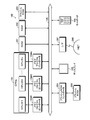
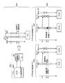
- FIG. 1 is an explanatory diagram illustrating an operation example when a failure occurs in the multi-core processor system 100 according to the present embodiment and an operation example of restoration processing.
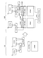
- FIG. 2 is a block diagram illustrating a hardware example of the multi-core processor system 100.
- FIG. 3 is a block diagram illustrating an example of functions of the multi-core processor system 100.
- FIG. 4 is an explanatory diagram showing an example of functions inside the memory protect controller 106.
- FIG. 5 is an explanatory diagram showing an example of registration of the memory protect controller 106.
- FIG. 6 is a flowchart illustrating an example of a processing procedure when the multi-core processor system 100 is activated.
- FIG. 1 is an explanatory diagram illustrating an operation example when a failure occurs in the multi-core processor system 100 according to the present embodiment and an operation example of restoration processing.
- FIG. 2 is a block diagram illustrating a hardware example of the multi-core processor system 100.
- FIG. 3 is a block diagram illustrating an example of functions of
- FIG. 7 is a flowchart (part 1) illustrating an example of a processing procedure when switching applications in the multi-core processor system 100.
- FIG. 8 is a flowchart (part 2) illustrating an example of a processing procedure when switching applications in the multi-core processor system 100.
- FIG. 9 is a flowchart illustrating an example of a processing procedure when an error occurs in the multi-core processor system 100.
- FIG. 10 is an explanatory diagram showing an operation example when software for a single core processor system operates on a multicore processor system.
- FIG. 11 is an explanatory diagram when a library that has been called on a single-core processor system is called on a multi-core processor system.
- FIG. 1 is an explanatory diagram illustrating an operation example when a failure occurs in the multi-core processor system 100 according to the present embodiment and an operation example of restoration processing.
- an explanatory diagram denoted by reference numeral 101 shows an operation example when a failure occurs in the multi-core processor system 100
- an explanatory diagram denoted by reference numeral 102 shows an operation example of restoration processing of the multi-core processor system 100.
- the multi-core processor system 100 in FIG. 1 includes CPUs 103 serving as a plurality of cores and a memory 104.
- the multi-core processor system 100 is assumed to be a mobile terminal such as a mobile phone.
- CPUs 103 include CPU # 1 and CPU # 2.
- the symbol accompanied by the suffix “#n” indicates that the symbol corresponds to the nth CPU.
- the CPUs 103 and the memory 104 are connected by a bus 105. Further, the CPU # 1 and the CPU # 2 can communicate with the memory protect controller 106 # 1 and the memory protect controller 106 # 2, respectively.
- the memory protect controller 106 is a device that operates according to the designated form of the two forms of the double access form and the access through form. When there is an instruction for a double access mode, the memory protect controller 106 has a function of accessing an address in the protected memory area while accessing the original request destination address of the application. When there is an instruction of the access through form, the memory protect controller 106 accesses the original request destination address of the application.
- the multi-core processor system 100 executes the low-reliability application 111 and the high-reliability application 112. Specifically, CPU # 1 executes the low-reliability application 111, and CPU # 2 executes the high-reliability application 112.
- the multi-core processor system 100 reserves a low-reliability application memory area 122 in the user area 121 as an area for storing the context of the low-reliability application 111.
- the multi-core processor system 100 reserves a highly reliable application memory area 123 in the user area 121 as an area in which the context of the highly reliable application 112 is stored.
- the context is data used by the application such as a program counter and a stack pointer that are values of the CPU registers.
- the multi-core processor system 100 secures a protect area 124 that is an area different from the user area 121, and secures a highly reliable application memory area 125 in the protect area 124.
- the highly reliable application memory area 125 stores the same data as the highly reliable application memory area 123.
- the CPU # 2 registers the double access mode in the memory protect controller 106 # 2 at the timing when the highly reliable application 112 executes.
- the memory protect controller 106 # 2 in the double access mode writes the written contents to the highly reliable application memory area 123 and also writes the same contents to the highly reliable application memory area 125.
- the low-reliability application 111 performs illegal writing and destroys the data in the high-reliability application memory area 123 with the high-reliability application memory area 123 protected as described above. is doing.
- the CPU # 2 tries to read and execute the high-reliability application memory area 123 when executing the high-reliability application 112, but the data in the high-reliability application memory area 123 does not indicate a correct value, 112 is forcibly terminated.
- the program counter in the high-reliability application memory area 123 is rewritten to an illegal address
- the CPU # 2 tries to execute the value of the illegal address as an execution code, and the high-reliability application 112 is forcibly terminated.
- the OS may hang other than when the trusted application 112 is forcibly terminated due to unauthorized writing.
- the operation when the OS hangs will be described with reference to FIG.
- an explanatory diagram denoted by reference numeral 102 shows a restoration process after data destruction.
- the CPU # 2 detects that an error has occurred in the highly reliable application 112, the CPU # 2 determines whether or not the highly reliable application 112 is being executed.
- the CPU # 2 compares the high-reliability application memory area 123 and the high-reliability application memory area 125. If there is a difference, the CPU # 2 sets the high-reliability application memory area 123 as the high-reliability application memory area 123. Overwrite with the memory area 125. As a result, the data that has been illegally written is restored to normal data, and the CPU # 2 can continue the high-reliability application 112, so that the high-reliability application 112 can be protected.
- FIG. 2 is a block diagram illustrating a hardware example of the multi-core processor system 100.
- the multi-core processor system 100 includes CPUs 103 equipped with a plurality of CPUs, a ROM (Read-Only Memory) 201, and a RAM (Random Access Memory) 202.
- the multi-core processor system 100 includes a flash ROM 203, a flash ROM controller 204, and a flash ROM 205.
- the memory 104 may be all or a part of the RAM 202. Further, the memory 104 may include a ROM 201, a flash ROM 203, and a flash ROM 205.
- the multi-core processor system 100 includes a display 206, an I / F (Interface) 207, and a keyboard 208 as input / output devices for users and other devices. Each unit is connected by a bus 105.
- the CPUs 103 control the entire multi-core processor system 100.
- the CPUs 103 refers to all CPUs in which single core processors are connected in parallel.
- the CPUs 103 include CPU # 1 to CPU #x.
- X is an integer of 2 or more.
- a multi-core processor system is a computer system including a processor having a plurality of cores. If a plurality of cores are mounted, a single processor having a plurality of cores may be used, or a processor group in which single core processors are arranged in parallel may be used. In the present embodiment, an example in which CPUs that are single-core processors are arranged in parallel will be described.
- CPU # 1 to CPU #x can communicate with the memory protect controller 106, respectively. Further, each of CPU # 1 to CPU #x may have a dedicated cache memory.
- the ROM 201 stores a program such as a boot program.
- the RAM 202 is used as a work area for the CPUs 103.
- the flash ROM 203 stores system software such as an OS (Operating System), application software, and the like.
- OS Operating System
- the multi-core processor system 100 receives the new OS by the I / F 207 and updates the old OS stored in the flash ROM 203 to the received new OS.
- the flash ROM controller 204 controls reading / writing of data with respect to the flash ROM 205 according to the control of the CPUs 103.
- the flash ROM 205 stores data written under the control of the flash ROM controller 204.
- data image data and video data acquired by the user using the multi-core processor system 100 through the I / F 207 and a program for executing the software protection method according to the present embodiment may be stored.
- the flash ROM 205 for example, a memory card, an SD card, or the like can be adopted.
- the display 206 displays data such as a document, an image, and function information as well as a cursor, an icon, or a tool box.
- the display 206 can employ a TFT liquid crystal display or the like.
- the I / F 207 is connected to a network 209 such as a LAN (Local Area Network), a WAN (Wide Area Network), or the Internet through a communication line, and is connected to another device via the network 209.
- the I / F 207 controls an internal interface with the network 209 and controls input / output of data from an external device.
- a modem or a LAN adapter can be used as the I / F 207.
- the keyboard 208 has keys for inputting numbers, various instructions, etc., and inputs data.
- the keyboard 208 may be a touch panel type input pad or a numeric keypad.
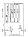
- FIG. 3 is a block diagram illustrating an example of functions of the multi-core processor system 100.
- the multi-core processor system 100 can access the reliable white list 301 as a storage area accessed from each function.
- the multi-core processor system 100 includes a securing unit 311, a detection unit 312, a comparison unit 313, a notification unit 314, a registration unit 315, a detection unit 316, a detection unit 317, a comparison unit 318, and a restoration unit 319.
- the functions (the securing unit 311 to the restoring unit 319) serving as the control unit realize the functions by the CPU # 1 to CPU #x executing the program stored in the storage device.
- the storage device is, for example, the ROM 201, the RAM 202, the flash ROM 203, the flash ROM 205, etc. shown in FIG.
- the function may be realized by execution by another CPU via the I / F 207.
- the securing unit 311 has the function of the CPU # 2 that executes the high-reliability application 112, but the function of any one of the CPU # 1, CPU # 3 to CPU #x There may be.
- the detection unit 312 to the restoration unit 319 may be functions included in all the CPUs CPU # 1 to CPU #x.
- the CPU # 2 executes hypervisor # 2, OS # 2, and kernel # 2.
- the hypervisor # 2 is a program that directly operates on hardware such as the CPU # 2.
- the hypervisor # 2 can execute a privileged instruction that directly refers to the register in the CPU # 2, reads the register information in the CPU # 2, and rewrites the register information in the CPU # 2. It is a program.
- the kernel # 2 is a core function of the OS # 2, for example, manages resources of the multi-core processor system 100 and allows software such as threads to access the hardware.
- OS # 2 is a program for controlling CPU # 2.
- a library that accesses resources in the multi-core processor system 100, an API (Application Programming Interface), and the like are provided to the application.
- API Application Programming Interface
- CPU # 1, CPU # 3 to CPU #x also execute the hypervisor, OS, and kernel.
- the securing unit 311 to the notification unit 314 and the detection unit 316 are included in the function of the kernel # 2
- the registration unit 315 and the detection unit 317 to the restoration unit 319 are included in the function of the hypervisor # 2.
- the high reliability white list 301 is a list for registering a predetermined application.
- the predetermined application to be registered is the high-reliability application 112 that has been verified for operation in the multi-core processor system 100.
- the high reliability application 112 is an application preinstalled in the multi-core processor system 100.
- an application provided by a manufacturer that manufactures the multi-core processor system 100, a communication carrier that provides the network 209, or the like may be registered as a highly reliable application. For example, when the multi-core processor system 100 downloads an application from the network 209 and the identification information indicating that the manufacturer or the communication carrier provides is attached, the downloaded application is registered in the reliable white list 301. Also good.
- the content registered in the high-reliability white list 301 may be, for example, the name of an application, or, if a file system exists, a file path in which the application program is stored.
- the securing unit 311 corresponds to a first memory area that is accessed by a plurality of CPUs when an application is executed at the time of system boot, and a second memory area that is similarly accessed when a plurality of CPUs access the first memory area.
- the first memory area is a memory area that is an access destination of the running application, and is the user area 121 shown in FIG.
- the second memory area becomes a protect area 124 that serves as an area for protecting data in the user area 121.
- the timing for securing the second memory may be at the time of system boot or when the application is activated.
- the multi-core processor system 100 assumes a mobile phone or the like, and does not assume that many applications are activated simultaneously.
- the maximum value of N is, for example, 8 or 16.
- N may be the number of CPUs 103.
- the address of the reserved area is stored in a storage area such as the register of the CPU # 2, the cache memory, and the RAM 202.
- the detection unit 312 has a function of detecting one of an event that the application has started, an event that the application has ended, and an event that the application has been switched. For example, the detection unit 312 detects an event that the highly reliable application 112 is activated. The detected event is stored in a storage area such as the register of CPU # 2, the cache memory, and the RAM 202.
- the comparison unit 313 has a function of comparing an application to be executed with an application registered in a predetermined application list when an event is detected by the detection unit 312. For example, the comparison unit 313 compares the high-reliability application 112 to be executed with the applications registered in the high-reliability white list 301.
- the comparison result is stored in a storage area such as a register of CPU # 2, a cache memory, and RAM 202.
- the notification unit 314 When the comparison result by the comparison unit 313 indicates a match, the notification unit 314 provides an instruction for the memory protect controller 106 # 2 to access the first memory region and the second memory region for the access from the application to be executed. It has a function to notify # 2. For example, it is assumed that the high-reliability application 112 and the application registered in the high-reliability white list 301 indicate a match. At this time, the notification unit 314 notifies the hypervisor # 2 of an instruction for the memory protect controller 106 # 2 to access the high-reliability application memory area 123 and the high-reliability application memory area 125 for access from the high-reliability application 112. .
- the notification unit 314 notifies the hypervisor # 2 of an instruction for the memory protect controller 106 # 2 to access the first memory area regarding the access from the executed application. May be.
- the notification unit 314 notifies the instruction to add the area for the activated application in the second memory area when the application is activated and the comparison result by the comparison unit 313 of the activated application indicates a match. Also good.
- the notification unit 314 may notify an instruction to release the completed application area in the second memory area when the application is completed and the comparison result of the completed application comparison unit 313 indicates a match. .
- the notified contents may be stored in a storage area such as a register of CPU # 2, a cache memory, or RAM 202.
- the registration unit 315 has a function of registering the instruction notified by the notification unit 314 in the memory protect controller 106 # 2. For example, when the instruction of the double access mode that is the first access mode is notified, the registration unit 315 registers the double access mode in the memory protect controller 106 # 2. Specifically, the registration unit 315 registers in a register in the memory protect controller 106 # 2.
- the registration unit 315 registers the access through form in the memory protect controller 106 # 2. Specific registration contents will be described with reference to FIG.
- the information indicating that the registration has been performed may be stored in a storage area such as the register of CPU # 2, the cache memory, and the RAM 202.
- the detecting unit 316 has a function of detecting that the application in the own CPU has been forcibly terminated. For example, the detection unit 316 detects that a highly reliable application 112 has been forcibly terminated due to a segment error or the like indicating that an inaccessible memory has been accessed. Information that the application has been forcibly terminated is stored in a storage area such as a register of CPU # 2, a cache memory, and RAM 202.
- the detection unit 317 has a function of detecting that OS # 2 is hung. For example, the detection unit 317 periodically monitors OS # 2, and detects that OS # 2 is hung when there is no response from OS # 2. Note that the OS being hung is in an abnormal state and cannot respond to the request.
- the OS hang state is also called kernel panic. Information that OS # 2 is hung is stored in a storage area such as a register of CPU # 2, a cache memory, and RAM202.
- the comparison unit 318 has a function of comparing the first memory area and the second memory area when the detection unit 316 detects forced termination of the application or when the detection unit 317 detects a hang of OS # 2. Have. For example, the comparison unit 318 compares the data in the high-reliability application memory area 123 and the high-reliability application memory area 125. Further, the comparison unit 318 may compare the first memory area and the second memory area when the application being executed is registered in the high-reliability white list 301. The comparison result is stored in a storage area such as a register of CPU # 2, a cache memory, and RAM 202.
- the restoration unit 319 has a function of restoring the first memory area based on the comparison result by the comparison unit 318. For example, when the comparison result by the comparison unit 318 indicates a mismatch, the restoration unit 319 restores the first memory area by overwriting the difference of the comparison result in the first memory area. Note that the result of the restoration may be stored in a storage area such as the register of the CPU # 2, the cache memory, or the RAM 202.
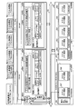
- FIG. 4 is an explanatory diagram showing an example of functions inside the memory protect controller 106.
- the memory protect controller 106 # 1 will be described as an example, but the memory protect controller 106 # 2 to the memory protect controller 106 # x also have the same functions as the memory protect controller 106 # 1.
- the memory protect controller 106 # 1 includes a storage unit 401 # 1, a determination unit 402 # 1, and a conversion unit 403 # 1.
- the storage unit 401 stores an access mode of the memory protect controller 106 and a protected area corresponding to the application.
- the storage unit 401 # 1 includes a control register 404 # 1 and storage registers 405 # 1_1 to 405 # 1_y.
- y is an integer of 1 or more.
- y may be the maximum value of the number of applications that can be executed simultaneously by CPU # 1.
- the multi-core processor system 100 according to the present embodiment is assumed to be a mobile phone or the like, and is not assumed to execute a large number of applications simultaneously like a personal computer. Therefore, the maximum number of applications that are simultaneously activated on each CPU is also a number that does not assume that many applications are activated simultaneously.
- y is a value of N or less. For example, y is a value such as 4 or 8.
- the control register 404 # 1 includes two fields: an access mode flag and a protected area management number.
- the access form flag field stores an identifier indicating access form information of either a double access form for accessing two addresses or an access through form for performing normal access. For example, as a specific identifier, “1” may mean a double access mode.
- the protected area management number field when two addresses are accessed, a value indicating which storage register 405 # 1 is applied among the storage registers 405 # 1_1 to 405 # 1_y is stored. For example, when “1” is stored in the protected area management number field, the conversion unit 403 # 1 performs conversion using the setting of the storage register 405 # 1_1.
- Storage registers 405 # 1_1 to 405 # 1_y are registers that store a protection area for each application. Further, the storage registers 405 # 1_1 to 405 # 1_y correspond to management number_1 to management number_y, respectively. Subsequently, each field of the storage register 405 # 1 will be described.
- the storage register 405 # 1 includes four fields: a used bit, an application ID, a mask address, and a protect address.
- in-use bit field a bit indicating whether or not the corresponding storage register 405 # 1 is in use is stored.
- application ID field identification information of an application being executed by CPU # 1 is stored.
- mask address field an address indicating a memory range accessed by the application is stored. The specific size of the memory range is determined by the memory management mechanism of the OS.
- protect address field an address to the protect area of the application being executed by the CPU # 1 is stored.
- the determination unit 402 # 1 has a function of determining whether or not to perform address conversion according to the access mode information stored in the storage unit 401 # 1. Specifically, the determination unit 402 # 1 accesses two addresses if the access form flag field is a double access form, and does not perform address conversion if the access form flag field is an access through form. , Address through.
- the conversion unit 403 # 1 has a function of performing address conversion for one access destination when the determination unit 402 # 1 determines that it is a double access mode. Specifically, the conversion unit 403 # 1 performs address conversion with reference to the mask address field of the storage register 405 # 1 corresponding to the management number set in the protected area management number field and the protected address field. For example, the conversion unit 403 converts the converted address according to the following equation (1).
- the conversion unit 403 performs conversion as follows according to (1).
- the memory protect controller 106 # 1 may perform a double access mode for the write request access among the read request access and the write request access from the CPU # 1. The reason is that even if a double access mode related to read request access is performed in the state where no error has occurred, the same value is returned, so that read access to an address for which conversion is not performed is sufficient.
- FIG. 5 is an explanatory diagram showing a registration example of the memory protect controller 106.
- the multi-core processor system 100 shown in FIG. 5 is registered in the high-reliability white list 301, and the applications A and C that are high-reliability apps and the low-reliability apps that are not registered in the high-reliability white list 301 B, app D, app E are running.
- Application A and application B are assigned to CPU # 1
- application C to application E are assigned to CPU # 2.
- CPU # 1 is executing application A
- CPU # 2 is executing application D.
- the application IDs of application A to application E are 0x0001, 0x0002, 0x0003, 0x0004, and 0x0005, respectively.
- Kernel # 1 reserves a memory area 0x00000000 to 0x00500000 as a kernel occupation area 501 when the OS boots. Subsequently, the kernel # 1 secures the protected area 124 before securing the user area 121 serving as the application operation space. For example, it is assumed that the number N of simultaneous application executions of the multi-core processor system 100 is 5 and the memory size M allowed for one application is 1 [M bytes].
- the protected area 124 is an area that cannot be accessed from the application. For this reason, for example, when the application A and the application B try to access the protected area 124 through the OS # 1, the kernel # 1 issues a segment error indicating that an unmanaged area of the OS # 1 is accessed. Become. As described above, the multi-core processor system 100 can prevent unauthorized writing of the protected area 124 by a low-reliability application by setting the protected area 124 to an area other than the user area 121.
- the area to be the protected area 124 may not be a continuous range and fixed, and may be secured in a distributed manner as long as the memory protect controller 106 can manage the dynamic area during execution of the multi-core processor system 100. It may change to. In the present embodiment, in order to simplify the description, the description will be made with the area serving as the protected area 124 being a continuous range and fixed.
- the multi-core processor system 100 reserves an area for storing the context of each application in the user area 121 when the applications A to E are activated.
- the kernel # 1 secures the application A memory area 502 when the application A is activated, and secures the application B memory area 503 when the application B is activated.
- the kernel # 2 secures the application C memory area 504 when the application C is activated, secures the application D memory area 505 when the application D is activated, and secures the application E memory area 506 when the application E is activated.
- the top addresses of the application A memory area 502 to the application E memory area 506 are 0x05000000, 0x05010000, 0x05020000, 0x05030000, and 0x05040000, respectively.
- the multi-core processor system 100 also secures a memory area in the protected area 124 when a highly reliable application is activated. Specifically, the hypervisor # 1 receiving the instruction from the kernel # 1 secures the application A memory area 507 when the application A is activated.
- the hypervisor # 1 sets a value in the storage register 405 # 1_1. Specifically, the hypervisor # 1 sets in use in the in use bit field and sets 0x0001, which is the application ID of the application A, in the application ID field. Subsequently, the hypervisor # 1 sets 0x0000ffff in the mask address field, and sets 0x01000000, which is the start address of the application A memory area 507, in the protect address field.
- the hypervisor # 2 reserves the application C memory area 508 when the application C is activated. Further, the hypervisor # 2 sets a value in the storage register 405 # 2_1. Specifically, the hypervisor # 2 sets in use in the in use bit field, and sets 0x0003, which is the application ID of the application C, in the application ID field. Subsequently, the hypervisor # 2 sets 0x0000ffff in the mask address field and sets 0x01020000 which is the start address of the application C memory area 508 in the protect address field.
- the multi-core processor system 100 finishes the application activation stage and transitions to a state in which it actually operates.
- CPU # 1 executes the applications in the order of application A, application B, application A,.
- kernel # 1 sets the access mode to the double access mode.
- the kernel # 1 also includes the switched application ID in the instruction content.
- the hypervisor # 1 Upon receipt of the instruction, the hypervisor # 1 registers the double access mode in the memory protect controller 106 # 1. Specifically, the hypervisor # 1 sets the access mode flag of the memory protect controller 106 # 1 to the double access mode. In addition, the hypervisor # 1 sets the management number of the storage register 405 # 1 that matches the instructed application ID in the protected area management number field. By such an operation, the multi-core processor system 100 synchronizes with the operation that can be switched between the application A, the application B,... By the OS # 1, and the double access mode and the access through mode by the memory protect controller 106 # 1. It works with ...
- the multi-core processor system 100 accesses two address spaces of 0x05000000 and 0x01000000.
- the bandwidth of CPU access is such that a bus of 128 [bit] band is set for a 64 [bit] CPU. This is a rough state where the entire bandwidth of the bus is not used. Therefore, by coordinating with the data packing function that combines two 64 [bit] accesses into one 128 [bit] in the bus 105, deterioration of bus access performance can be avoided.
- CPU # 2 executes the application in the order of application C, application D, application E, application C,.
- the application D is not registered in the high-reliability white list 301. Therefore, the kernel # 2 generates an application switching event and sets the access mode to the access-through mode.
- the kernel # 2 includes the switched application ID in the instruction content.
- the hypervisor # 2 registers the access through form in the memory protect controller 106 # 2. Specifically, the hypervisor # 2 sets the access form flag of the memory protect controller 106 # 2 to the access through form.
- the execution subject that executes an example of the processing procedure at the time of startup shown in FIG. 6 may be any CPU among CPU # 1 to CPU #x, but for simplification of explanation, CPU # 1
- the description will be made assuming the case of execution.
- the execution subject that executes the application switching processing procedure and the error processing procedure shown in FIGS. 7 to 9 is executed by all CPUs CPU # 1 to CPU #x. Therefore, description will be made assuming that CPU # 1 executes.
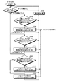
- FIG. 6 is a flowchart illustrating an example of a processing procedure when the multi-core processor system 100 is started up.
- the kernel # 1 starts to boot (step S601)
- the kernel # 1 starts the memory management mechanism (step S602).
- the kernel # 1 reserves an address space of N ⁇ M [bytes] by the memory management mechanism (step S603).
- the kernel # 1 After securing, the kernel # 1 notifies the secured address space to the hypervisor # 1 (step S604), performs normal operation (step S605), and ends the processing at the time of startup. Note that in normal operation, the user area 121 is secured, or an application that is started at the beginning of booting is started.
- the hypervisor # 1 Upon receiving the notification of the address space, the hypervisor # 1 sets the notified address space as the protected area 124 (step S606), and ends the processing at the time of activation. Thereby, the multi-core processor system 100 can secure a memory protection area of a highly reliable application.
- FIG. 7 and 8 show an example of a processing procedure when switching the application of the multi-core processor system 100.
- FIG. FIG. 7 shows an example of the processing procedure of the kernel # 1
- FIG. 8 shows an example of the processing procedure of the hypervisor # 1.
- FIG. 7 is a flowchart (part 1) illustrating an example of a processing procedure when switching applications in the multi-core processor system 100.
- the kernel # 1 determines whether or not an event has occurred (step S701). If no event has occurred (step S701: no event has occurred), the kernel # 1 executes step S701 again after a predetermined time. Note that the kernel # 1 may execute another process of the kernel # 1 at a certain time.
- step S701 application activation event
- step S702 determines whether the activated application is registered in the reliable white list 301 (step S702). If registered (step S702: Yes), the kernel # 1 notifies the hypervisor # 1 of an instruction to add a management number (step S704). In step S704, the kernel # 1 includes the application ID of the activated application in the instruction content.
- kernel # 1 executes normal processing (step S703), and proceeds to the processing of step S701. If not registered (step S702: No), the kernel # 1 proceeds to the process of step S703.
- the normal process of the application activation event is, for example, a process of securing an area for storing the context of the activated application in the user area 121.
- step S701 application end event
- step S705 the kernel # 1 determines whether or not the ended application is registered in the reliable white list 301 (step S705). If registered (step S705: Yes), the kernel # 1 notifies the hypervisor # 1 of a management number release instruction (step S706). In step S706, kernel # 1 includes the application ID of the completed application in the instruction content.
- step S705 After notification or if not registered (step S705: No), the kernel # 1 proceeds to the process of step S703.
- the normal process of the application end event is, for example, a process of releasing an area for storing the context of the completed application that is secured in the user area 121.
- step S701 application switching event
- the kernel # 1 determines whether or not the switched application is registered in the reliable white list 301 (step S707). If registered (step S707: Yes), the kernel # 1 notifies the hypervisor # 1 of a dual access mode instruction (step S708). In step S708, kernel # 1 includes the application ID of the application after switching in the instruction content. After the notification, the kernel # 1 proceeds to the process of step S703. If not registered (step S707: No), the kernel # 1 notifies the hypervisor # 1 of an access through type instruction (step S709). After the notification, the kernel # 1 proceeds to the process of step S703.
- the CPU registers and the like are saved in the area for storing the context of the application before switching, and the value of the register saved in the area for storing the context of the application after switching is set in the CPU register.
- the multi-core processor system 100 can instruct the memory protection controller 106 to change the setting in response to an event such as application activation, termination, and switching.
- FIG. 8 is a flowchart (part 2) illustrating an example of a processing procedure at the time of application switching in the multi-core processor system 100.
- the hypervisor # 1 sets the control register 404 # 1 and the storage register 405 # 1 in the memory protect controller 106 # 1. Therefore, in the description of each step, for the sake of simplification of description, description that the setting destination register is a register in the memory protect controller 106 # 1 is omitted.
- Hypervisor # 1 confirms the instruction content (step S801). If the instruction content is an instruction to add a management number (step S801: an instruction to add a management number), the hypervisor # 1 uses an unused storage register 405 # 1 among the storage registers 405 # 1_1 to 405 # 1_y. Is determined (step S802).
- step S802 If there is an unused storage register 405 # 1 (step S802: Yes), the hypervisor # 1 sets the in-use bit field of the found storage register 405 # 1 to being used (step S803). Subsequently, the hypervisor # 1 sets the application ID field of the found storage register 405 # 1 to the application ID included in the instruction content (step S804). Further, the hypervisor # 1 sets an unassigned address in the protected address field of the found storage register 405 # 1 (step S805), and proceeds to the process of step S801. When the storage register 405 # 1 does not exist (step S802: No), the hypervisor # 1 proceeds to the process of step S801.
- the unallocated address in the process of step S805 is an address of a memory area that is not allocated as a memory area of another highly reliable application in the protected area 124.
- the mask address in the present embodiment is always a fixed value. Therefore, for example, in step S606 described above, hypervisor # 1 sets 0x0000ffff in the mask address fields of storage registers 405 # 1_1 to 405 # 1_y as the setting location of the mask address field.
- the hypervisor # 1 When the instruction content is a management number release instruction (step S801: management number release instruction), the hypervisor # 1 includes the application ID field in the instruction content among the storage registers 405 # 1_1 to 405 # 1_y. The storage register 405 # 1 that matches the application ID that has been stored is selected (step S806). After selection, the hypervisor # 1 sets the value of the protected address field of the selected storage register 405 # 1 to an unassigned address (step S807). Subsequently, the hypervisor # 1 sets the in-use bit field of the selected storage register 405 # 1 to unused (step S808), and proceeds to the processing of step S801.
- step S801 dual access mode instruction
- the hypervisor # 1 stores the application ID field of the storage register 405 # 1 that matches the application ID included in the instruction content.
- the management number is set in the protect management number field (step S809).
- the hypervisor # 1 sets the access mode flag to the double access mode (step S810), and proceeds to the process of step S801.
- step S801 access through type instruction
- the hypervisor # 1 sets the access type flag to the access through type (step S811), and proceeds to the process of step S801.
- the multi-core processor system 100 changes the access mode in synchronization with each event of the application in order to change the setting to the memory protection controller 106 in response to an event such as activation, termination, and switching of the application. it can.
- FIG. 9 illustrates an example of a processing procedure when an error occurs.
- the operation verification of the low-reliability application executed by CPU # 2 was insufficient, it is assumed that a failure occurs as a result of the low-reliability application writing to another memory area. Yes.
- the first state is a state where a highly reliable application is terminated with a simple program error. For example, when an error occurs with respect to a highly reliable application running on OS # 1, OS # 1 can detect the occurrence of the error and notify hypervisor # 1.
- the second state is when OS # 1 hangs. When OS # 1 hangs, it is impossible to detect the failure state of a highly reliable application. Therefore, the hypervisor # 1 operating independently of the OS # 1 detects whether the OS # 1 is hung by the period monitoring.
- FIG. 9 is a flowchart illustrating an example of a processing procedure when an error occurs in the multi-core processor system 100.
- the kernel # 2 executes the low reliability application (step S901). It is assumed that illegal execution is performed in the user area 121 by this execution and a failure occurs.
- kernel # 1 detects a segment error (step S902). After detection, the kernel # 1 temporarily stops the multi-core processor system 100 (step S903), and instructs the hypervisor # 1 to perform recovery notification (step S904).
- the hypervisor # 1 determines whether the running application is registered in the reliable white list 301 or not. Is determined (step S905). If registered (step S905: Yes), the hypervisor # 1 compares the data in the memory area of the running application in the protected area 124 with the data in the memory area of the running application in the user area 121 (step S906). .
- the hypervisor # 1 determines whether or not the comparison results match (step S907). If they do not match (step S907: No), the hypervisor # 1 restores the data of the running application in the user area 121 (step S908). Specifically, the hypervisor # 1 overwrites the difference of the comparison result in the memory area of the running application in the user area 121. As a result, data that has been illegally written is restored to normal data.
- step S905 If it is not registered in the high-reliability white list 301 (step S905: No), if the comparison results match (step S907: Yes), or after data restoration, the hypervisor # 1 is hung OS # 1 It is determined whether or not (step S909). If it is hung (step S909: Yes), the hypervisor # 1 performs a warm start of the OS # 1 (step S910), and ends the processing at the time of the error. As a specific warm start method, checkpoint restart technology or hibernation technology can be applied.
- step S909 the hypervisor # 1 notifies the kernel # 1 that the multicore processor system 100 is released from the suspension (step S911), and ends the processing at the time of the error.
- the kernel # 1 which has received the suspension cancellation, cancels the suspension of the multi-core processor system 100 (step S912), and ends the processing at the time of the error.
- the multi-core processor system 100 can restore the data and continue the operation when an error occurs in the high-reliability application due to the memory destruction due to the illegal writing.
- the multi-core processor system can perform recovery by using both the high-reliability app and the low-reliability application because the low-reliability app can destroy the first memory area and recover using the second memory area even if a failure occurs. .
- the software protection method executed by the multi-core processor system according to the present embodiment can safely inherit the software assets in the single-core processor system to the multi-core processor system environment.
- the multi-core processor system according to the present embodiment is operated in a normal operation state without occurrence of biased unfavorable scheduling such as not causing a low-reliability app to be executed during execution of a high-reliability app. Can do.
- a recovery process occurs when a failure occurs, and a load-intensive process is not executed in a normal operation state, so that the overall performance is not deteriorated.
- the multi-core processor system can access a list that stores a predetermined application, and may compare an application to be executed with an application stored in the list. Thereby, the multi-core processor system can determine whether or not the application to be executed is a highly reliable application.
- the multi-core processor system has a memory protection controller corresponding to a CPU that executes an application so as to access the first memory area and the second memory area when the application to be executed matches the application stored in the list. You may register. Thereby, the multi-core processor system can protect data of a highly reliable application.
- the multi-core processor system may register with the memory protect controller corresponding to the CPU executing the application so as to access the first memory area when the application to be executed and the application stored in the list do not match.
- the multi-core processor system can effectively use the protected area reserved for data protection without protecting the data for the low-reliability application that does not need to protect the data.
- the multi-core processor system may restore the first memory area based on the comparison result between the first memory area and the second memory area in response to the abnormality detection of the own system. Thereby, the multi-core processor system can recover the faulty application.
- the multi-core processor system may protect an app that has been verified for operation in a multi-core processor system environment as a highly reliable app.
- An unreliable application may destroy the first memory area itself.
- the second memory area is also destroyed.
- the multi-core processor system can recover the failure of the high-reliability app generated by the operation of the low-reliability app by targeting the high-reliability app verified as having no defects.
- the present embodiment can be applied even if the target is a library. Can do.
- the software protection method executed by the multi-core processor system described in this embodiment can be realized by executing a program prepared in advance on a computer such as a personal computer or a workstation.
- a software protection program for executing the software protection method is recorded on a computer-readable recording medium such as a hard disk, a CD-ROM, a DVD, or a memory card, and is executed by being read from the recording medium by the computer.
- the software protection program may be distributed through a network such as the Internet.
- the memory protect controller 106 described in the present embodiment is a special purpose IC (hereinafter simply referred to as “ASIC”) such as a standard cell or a structured ASIC (Application Specific Integrated Circuit), or a PLD (Programmable) such as an FPGA. It can also be realized by Logic Device. Specifically, for example, the function (memory unit 401 to conversion unit 403) of the above-described memory protect controller 106 is defined by HDL description, and the HDL description is logically synthesized and given to the ASIC or PLD to protect the memory. Controller 106 can be manufactured.
Abstract
Description
図2は、マルチコアプロセッサシステム100のハードウェア例を示すブロック図である。図2において、マルチコアプロセッサシステム100は、CPUを複数搭載するCPUs103と、ROM(Read‐Only Memory)201と、RAM(Random Access Memory)202と、を含む。また、マルチコアプロセッサシステム100は、フラッシュROM203と、フラッシュROMコントローラ204と、フラッシュROM205と、を含む。なお、メモリ104は、RAM202の全てであってもよいし、または一部であってもよい。さらに、メモリ104は、ROM201、フラッシュROM203、フラッシュROM205を含んでいてもよい。
次に、マルチコアプロセッサシステム100の機能例について説明する。図3は、マルチコアプロセッサシステム100の機能例を示すブロック図である。なお、マルチコアプロセッサシステム100は、各機能からアクセスされる記憶領域として、高信頼ホワイトリスト301にアクセス可能である。
⇔変換後のアドレス=0x01000100
100 マルチコアプロセッサシステム
104 メモリ
105 バス
106 メモリプロテクトコントローラ
111 低信頼アプリ
112 高信頼アプリ
121 ユーザ領域
122 低信頼アプリメモリ領域
123 高信頼アプリメモリ領域
124 プロテクト領域
125 高信頼アプリメモリ領域
301 高信頼ホワイトリスト
311 確保部
312 検出部
313 比較部
314 通知部
315 登録部
316 検出部
317 検出部
318 比較部
319 復元部
Claims (10)
- 複数のCPUと、
メモリと、
前記複数のCPUと前記メモリとの間に配置されるメモリプロテクトコントローラと、
を含み、
前記メモリプロテクトコントローラは、
アプリケーション実行時に前記複数のCPUのアクセス要求によって第1メモリ領域にアクセスするとともに、システムブート時に確保された第2メモリ領域にアクセスすること
を特徴とするマルチコアプロセッサシステム。 - 所定のアプリケーションのリストを格納するテーブルと、
実行されるアプリケーションと前記リストのアプリケーションとを比較する比較部と、
を含むことを特徴とする請求項1に記載のマルチコアプロセッサシステム。 - 比較結果が一致を示すとき、前記実行されるアプリケーションについて、前記第1メモリ領域と前記第2メモリ領域とをアクセスする指示を登録すること
を特徴とする請求項2に記載のマルチコアプロセッサシステム。 - 比較結果が不一致を示すとき、前記実行されるアプリケーションについて、前記第1メモリ領域のみをアクセスする指示を登録すること
を特徴とする請求項2に記載のマルチコアプロセッサシステム。 - 自システムの異常の検出に応答して、前記実行されるアプリケーションが実行中であるときに前記第1メモリ領域と前記第2メモリ領域との比較結果に基づいて前記第1メモリ領域を復元すること
を特徴とする請求項1乃至請求項4の何れか一に記載のマルチコアプロセッサシステム。 - 前記所定のアプリケーションは、マルチコアプロセッサシステム環境での動作検証が行われたアプリケーションであること
を特徴とする請求項1乃至請求項5の何れか一に記載のマルチコアプロセッサシステム。 - 前記複数のCPUの数がN(Nは2以上の整数)であり、アプリケーション実行時に割り当てられる前記メモリのメモリ領域がM(Mは1以上の整数)バイトであるとき、前記第2メモリ領域の大きさはN×Mであること
を特徴とする請求項1乃至請求項6の何れか一に記載のマルチコアプロセッサシステム。 - 複数のCPUと、
メモリと、
前記複数のCPUと前記メモリとの間に配置されるメモリプロテクトコントローラと、
を含み、
前記メモリプロテクトコントローラは、
アクセス形態情報が第1アクセス形態を示す場合には、アプリケーション実行において第1メモリ領域へのアクセスと同様に第2メモリ領域をアクセスし、
アクセス形態情報が第2アクセス形態を示す場合には、アプリケーション実行において前記第1メモリ領域のみをアクセスすること
を特徴とするマルチコアプロセッサシステム。 - 前記アプリケーションとリストに登録されるアプリケーションとの比較結果に基づいて前記アクセス形態情報が設定されること
を特徴とする請求項8に記載のマルチコアプロセッサシステム。 - 前記比較結果が一致を示すとき、前記アクセス形態情報が第1アクセス形態に設定され、
前記比較結果が不一致を示すとき、前記アクセス形態情報が第2アクセス形態に設定されること
を特徴とする請求項9に記載のマルチコアプロセッサシステム。
Priority Applications (4)
| Application Number | Priority Date | Filing Date | Title |
|---|---|---|---|
| PCT/JP2011/057715 WO2012131884A1 (ja) | 2011-03-28 | 2011-03-28 | マルチコアプロセッサシステム |
| CN201180069869.6A CN103493022B (zh) | 2011-03-28 | 2011-03-28 | 多核处理器系统 |
| JP2013506906A JP5716824B2 (ja) | 2011-03-28 | 2011-03-28 | マルチコアプロセッサシステム |
| US14/036,758 US20140025903A1 (en) | 2011-03-28 | 2013-09-25 | Multi-core processor system |
Applications Claiming Priority (1)
| Application Number | Priority Date | Filing Date | Title |
|---|---|---|---|
| PCT/JP2011/057715 WO2012131884A1 (ja) | 2011-03-28 | 2011-03-28 | マルチコアプロセッサシステム |
Related Child Applications (1)
| Application Number | Title | Priority Date | Filing Date |
|---|---|---|---|
| US14/036,758 Continuation US20140025903A1 (en) | 2011-03-28 | 2013-09-25 | Multi-core processor system |
Publications (1)
| Publication Number | Publication Date |
|---|---|
| WO2012131884A1 true WO2012131884A1 (ja) | 2012-10-04 |
Family
ID=46929719
Family Applications (1)
| Application Number | Title | Priority Date | Filing Date |
|---|---|---|---|
| PCT/JP2011/057715 WO2012131884A1 (ja) | 2011-03-28 | 2011-03-28 | マルチコアプロセッサシステム |
Country Status (4)
| Country | Link |
|---|---|
| US (1) | US20140025903A1 (ja) |
| JP (1) | JP5716824B2 (ja) |
| CN (1) | CN103493022B (ja) |
| WO (1) | WO2012131884A1 (ja) |
Families Citing this family (5)
| Publication number | Priority date | Publication date | Assignee | Title |
|---|---|---|---|---|
| US9760712B2 (en) * | 2014-05-23 | 2017-09-12 | Vmware, Inc. | Application whitelisting using user identification |
| US10387668B2 (en) | 2014-07-08 | 2019-08-20 | International Business Machines Corporation | Data protected process cores |
| JP6360387B2 (ja) * | 2014-08-19 | 2018-07-18 | ルネサスエレクトロニクス株式会社 | プロセッサシステム、エンジン制御システム及び制御方法 |
| CN104199777B (zh) * | 2014-09-11 | 2017-10-03 | 福州瑞芯微电子股份有限公司 | 一种中央处理器系统验证方法及装置 |
| CN112462926B (zh) * | 2020-12-09 | 2021-07-30 | 北京元心科技有限公司 | 移动终端中的电源管理方法、装置、电子设备及计算机存储介质 |
Citations (6)
| Publication number | Priority date | Publication date | Assignee | Title |
|---|---|---|---|---|
| JPH05108493A (ja) * | 1991-10-17 | 1993-04-30 | Shikoku Nippon Denki Software Kk | メモリ制御方式 |
| JPH05143467A (ja) * | 1991-11-22 | 1993-06-11 | Mitsubishi Electric Corp | 冗長構成切替方法および冗長構成切替装置 |
| JP2003316752A (ja) * | 2002-04-25 | 2003-11-07 | Nec Corp | マルチプロセッサシステムおよびリソース割り当て方法 |
| JP2009251967A (ja) * | 2008-04-07 | 2009-10-29 | Toyota Motor Corp | マルチコアシステム |
| JP2009271597A (ja) * | 2008-04-30 | 2009-11-19 | Toshiba Corp | プロセッサ |
| JP2010118010A (ja) * | 2008-11-14 | 2010-05-27 | Nomura Research Institute Ltd | 情報取得仲介プログラム、オペレーティングシステム、情報取得仲介方法 |
Family Cites Families (10)
| Publication number | Priority date | Publication date | Assignee | Title |
|---|---|---|---|---|
| US6449699B2 (en) * | 1999-03-29 | 2002-09-10 | International Business Machines Corporation | Apparatus and method for partitioned memory protection in cache coherent symmetric multiprocessor systems |
| JP3968227B2 (ja) * | 2001-10-05 | 2007-08-29 | ソフトバンクテレコム株式会社 | 情報処理方法および情報処理装置 |
| US7149862B2 (en) * | 2002-11-18 | 2006-12-12 | Arm Limited | Access control in a data processing apparatus |
| US20050080999A1 (en) * | 2003-10-08 | 2005-04-14 | Fredrik Angsmark | Memory interface for systems with multiple processors and one memory system |
| EP1763744B1 (en) * | 2004-04-30 | 2017-07-19 | BlackBerry Limited | System and method of owner application control of electronic devices |
| US7406711B2 (en) * | 2005-09-02 | 2008-07-29 | Motorola, Inc. | Method and apparatus for enforcing independence of processors on a single IC |
| US7953914B2 (en) * | 2008-06-03 | 2011-05-31 | International Business Machines Corporation | Clearing interrupts raised while performing operating system critical tasks |
| US8296526B2 (en) * | 2009-06-17 | 2012-10-23 | Mediatek, Inc. | Shared memory having multiple access configurations |
| CN201716716U (zh) * | 2009-12-15 | 2011-01-19 | 深圳市杰和科技发展有限公司 | 一种基本输入输出系统只读存储器数据的备份系统 |
| US8438338B2 (en) * | 2010-08-15 | 2013-05-07 | International Business Machines Corporation | Flexible use of extended cache using a partition cache footprint |
-
2011
- 2011-03-28 WO PCT/JP2011/057715 patent/WO2012131884A1/ja active Application Filing
- 2011-03-28 JP JP2013506906A patent/JP5716824B2/ja not_active Expired - Fee Related
- 2011-03-28 CN CN201180069869.6A patent/CN103493022B/zh not_active Expired - Fee Related
-
2013
- 2013-09-25 US US14/036,758 patent/US20140025903A1/en not_active Abandoned
Patent Citations (6)
| Publication number | Priority date | Publication date | Assignee | Title |
|---|---|---|---|---|
| JPH05108493A (ja) * | 1991-10-17 | 1993-04-30 | Shikoku Nippon Denki Software Kk | メモリ制御方式 |
| JPH05143467A (ja) * | 1991-11-22 | 1993-06-11 | Mitsubishi Electric Corp | 冗長構成切替方法および冗長構成切替装置 |
| JP2003316752A (ja) * | 2002-04-25 | 2003-11-07 | Nec Corp | マルチプロセッサシステムおよびリソース割り当て方法 |
| JP2009251967A (ja) * | 2008-04-07 | 2009-10-29 | Toyota Motor Corp | マルチコアシステム |
| JP2009271597A (ja) * | 2008-04-30 | 2009-11-19 | Toshiba Corp | プロセッサ |
| JP2010118010A (ja) * | 2008-11-14 | 2010-05-27 | Nomura Research Institute Ltd | 情報取得仲介プログラム、オペレーティングシステム、情報取得仲介方法 |
Also Published As
| Publication number | Publication date |
|---|---|
| JPWO2012131884A1 (ja) | 2014-07-24 |
| CN103493022A (zh) | 2014-01-01 |
| CN103493022B (zh) | 2016-05-04 |
| JP5716824B2 (ja) | 2015-05-13 |
| US20140025903A1 (en) | 2014-01-23 |
Similar Documents
| Publication | Publication Date | Title |
|---|---|---|
| EP2989579B1 (en) | Redundant system boot code in a secondary non-volatile memory | |
| US9880908B2 (en) | Recovering from compromised system boot code | |
| JP4916576B2 (ja) | マルチオペレーティングシステム(os)起動装置及びマルチos起動プログラム及び記録媒体及びマルチos起動方法 | |
| US10733288B2 (en) | Verifying controller code and system boot code | |
| US8028174B2 (en) | Controlling update of content of a programmable read-only memory | |
| JP5203967B2 (ja) | メモリ障害を処理するために、センサーネットワークで使用可能な方法及びシステム | |
| US10032029B2 (en) | Verifying integrity of backup file in a multiple operating system environment | |
| JP6736456B2 (ja) | 情報処理装置およびプログラム | |
| US9205809B2 (en) | Vehicle unit and method for operating the vehicle unit | |
| US8146150B2 (en) | Security management in multi-node, multi-processor platforms | |
| US8327415B2 (en) | Enabling byte-code based image isolation | |
| JP5716824B2 (ja) | マルチコアプロセッサシステム | |
| WO2015174512A1 (ja) | 情報処理装置、情報処理監視方法、プログラム、及び記録媒体 | |
| JP6984710B2 (ja) | コンピュータ装置およびメモリ管理方法 | |
| JP2009157542A (ja) | 情報処理装置及びそのスタックポインタ更新方法 | |
| WO2007022687A1 (fr) | Système et procédé de contrôle de sécurité de système d’exploitation | |
| JP5920509B2 (ja) | コントローラの制御プログラム、およびコントローラの制御方法 | |
| WO2010032330A1 (ja) | 情報処理装置及びそのメモリ保護方法 | |
| US20080313489A1 (en) | Flash memory-hosted local and remote out-of-service platform manageability | |
| JP6462540B2 (ja) | ドライバ装置、情報処理システム、プログラムおよび方法 | |
| JP5565187B2 (ja) | 情報処理装置および割込み制御プログラム | |
| JP2020140689A (ja) | 計算機、オペレーティングシステム及び方法 | |
| US20240134720A1 (en) | Apparatus, and method | |
| JP5454686B2 (ja) | マルチコアプロセッサシステム、復元プログラム、および復元方法 | |
| JP2009271597A (ja) | プロセッサ |
Legal Events
| Date | Code | Title | Description |
|---|---|---|---|
| WWE | Wipo information: entry into national phase |
Ref document number: 201180069869.6 Country of ref document: CN |
|
| 121 | Ep: the epo has been informed by wipo that ep was designated in this application |
Ref document number: 11862026 Country of ref document: EP Kind code of ref document: A1 |
|
| ENP | Entry into the national phase |
Ref document number: 2013506906 Country of ref document: JP Kind code of ref document: A |
|
| NENP | Non-entry into the national phase |
Ref country code: DE |
|
| 122 | Ep: pct application non-entry in european phase |
Ref document number: 11862026 Country of ref document: EP Kind code of ref document: A1 |