WO2012127956A1 - 演算増幅器回路並びにそれを用いた表示パネルドライバ及び表示装置 - Google Patents
演算増幅器回路並びにそれを用いた表示パネルドライバ及び表示装置 Download PDFInfo
- Publication number
- WO2012127956A1 WO2012127956A1 PCT/JP2012/053937 JP2012053937W WO2012127956A1 WO 2012127956 A1 WO2012127956 A1 WO 2012127956A1 JP 2012053937 W JP2012053937 W JP 2012053937W WO 2012127956 A1 WO2012127956 A1 WO 2012127956A1
- Authority
- WO
- WIPO (PCT)
- Prior art keywords
- channel
- channel mos
- voltage
- differential pair
- amplifier circuit
- Prior art date
- Legal status (The legal status is an assumption and is not a legal conclusion. Google has not performed a legal analysis and makes no representation as to the accuracy of the status listed.)
- Ceased
Links
Images





Classifications
-
- H—ELECTRICITY
- H03—ELECTRONIC CIRCUITRY
- H03F—AMPLIFIERS
- H03F3/00—Amplifiers with only discharge tubes or only semiconductor devices as amplifying elements
- H03F3/45—Differential amplifiers
- H03F3/45071—Differential amplifiers with semiconductor devices only
- H03F3/45076—Differential amplifiers with semiconductor devices only characterised by the way of implementation of the active amplifying circuit in the differential amplifier
- H03F3/45179—Differential amplifiers with semiconductor devices only characterised by the way of implementation of the active amplifying circuit in the differential amplifier using MOSFET transistors as the active amplifying circuit
- H03F3/45183—Long tailed pairs
-
- G—PHYSICS
- G09—EDUCATION; CRYPTOGRAPHY; DISPLAY; ADVERTISING; SEALS
- G09G—ARRANGEMENTS OR CIRCUITS FOR CONTROL OF INDICATING DEVICES USING STATIC MEANS TO PRESENT VARIABLE INFORMATION
- G09G3/00—Control arrangements or circuits, of interest only in connection with visual indicators other than cathode-ray tubes
- G09G3/20—Control arrangements or circuits, of interest only in connection with visual indicators other than cathode-ray tubes for presentation of an assembly of a number of characters, e.g. a page, by composing the assembly by combination of individual elements arranged in a matrix no fixed position being assigned to or needed to be assigned to the individual characters or partial characters
- G09G3/34—Control arrangements or circuits, of interest only in connection with visual indicators other than cathode-ray tubes for presentation of an assembly of a number of characters, e.g. a page, by composing the assembly by combination of individual elements arranged in a matrix no fixed position being assigned to or needed to be assigned to the individual characters or partial characters by control of light from an independent source
- G09G3/36—Control arrangements or circuits, of interest only in connection with visual indicators other than cathode-ray tubes for presentation of an assembly of a number of characters, e.g. a page, by composing the assembly by combination of individual elements arranged in a matrix no fixed position being assigned to or needed to be assigned to the individual characters or partial characters by control of light from an independent source using liquid crystals
- G09G3/3611—Control of matrices with row and column drivers
- G09G3/3685—Details of drivers for data electrodes
- G09G3/3688—Details of drivers for data electrodes suitable for active matrices only
-
- H—ELECTRICITY
- H03—ELECTRONIC CIRCUITRY
- H03F—AMPLIFIERS
- H03F2203/00—Indexing scheme relating to amplifiers with only discharge tubes or only semiconductor devices as amplifying elements covered by H03F3/00
- H03F2203/45—Indexing scheme relating to differential amplifiers
- H03F2203/45366—Indexing scheme relating to differential amplifiers the AAC comprising multiple transistors parallel coupled at their gates only, e.g. in a cascode dif amp, only those forming the composite common source transistor
-
- H—ELECTRICITY
- H03—ELECTRONIC CIRCUITRY
- H03F—AMPLIFIERS
- H03F2203/00—Indexing scheme relating to amplifiers with only discharge tubes or only semiconductor devices as amplifying elements covered by H03F3/00
- H03F2203/45—Indexing scheme relating to differential amplifiers
- H03F2203/45506—Indexing scheme relating to differential amplifiers the CSC comprising only one switch
-
- H—ELECTRICITY
- H03—ELECTRONIC CIRCUITRY
- H03F—AMPLIFIERS
- H03F2203/00—Indexing scheme relating to amplifiers with only discharge tubes or only semiconductor devices as amplifying elements covered by H03F3/00
- H03F2203/45—Indexing scheme relating to differential amplifiers
- H03F2203/45646—Indexing scheme relating to differential amplifiers the LC comprising an extra current source
-
- H—ELECTRICITY
- H03—ELECTRONIC CIRCUITRY
- H03F—AMPLIFIERS
- H03F2203/00—Indexing scheme relating to amplifiers with only discharge tubes or only semiconductor devices as amplifying elements covered by H03F3/00
- H03F2203/45—Indexing scheme relating to differential amplifiers
- H03F2203/45674—Indexing scheme relating to differential amplifiers the LC comprising one current mirror
Definitions
- the present invention relates to an operational amplifier circuit, a display panel driver and a display device using the operational amplifier circuit, and more particularly to improvement of transient characteristics of the operational amplifier circuit.
- one of circuits that significantly affects the image quality of a display image is an operational amplifier circuit used as an output amplifier.
- an operational amplifier circuit used as an output amplifier.
- Rail-to-Rail operation As an output amplifier of a panel display device, there is an operational amplifier circuit corresponding to a so-called Rail-to-Rail operation that allows any of an input voltage and an output voltage to take any voltage from a negative power supply voltage to a positive power supply voltage.
- Rail-to-Rail operation There are two known circuit configurations for realizing Rail-to-Rail operation: one is a differential pair of P-channel MOS transistors (also referred to as a “P-channel differential pair”) in the input differential stage. And a differential pair of N-channel MOS transistors (also referred to as “N-channel differential pair”), and the other is only a differential pair of depletion type N-channel MOS transistors. It is the structure to provide.
- FIG. 1 is a circuit diagram showing a circuit configuration of a typical Rail-to-Rail amplifier in which both a P-channel MOS transistor differential pair and an N-channel MOS transistor differential pair are provided in an input differential stage.
- the circuit configuration as shown in FIG. 1 is disclosed, for example, in US Pat. No. 5,311,145, and is described as a reference circuit in textbooks of CMOS analog circuits and prominent documents other than this patent document. Yes.
- the circuit configuration of this operational amplifier is roughly divided into an input differential stage (first stage), an intermediate stage, and a final stage.
- the input differential stage includes an N-channel differential pair formed by N-channel MOS transistors MN1 and MN2, and a P-channel differential pair formed by P-channel MOS transistors MP1 and MP2.
- N-channel MOS transistors MN1, MN2 has a source connected in common, between the commonly connected sources and the negative supply voltage V SS terminal (ground terminal), the constant current source I1 is connected.
- the P channel MOS transistors MP1 and MP2 have their sources connected in common, and a constant current source I2 is connected between the commonly connected source and the power supply terminal of the positive power supply voltage V DD .
- the intermediate stage has two folded cascode current mirrors that function as active loads, and a floating current source I3.
- P-channel MOS transistors MP3 to MP6 constitute a first folded cascode current mirror
- N-channel MOS transistors MN3 to MN6 constitute a second folded cascode current mirror.
- the constant voltage source V1 supplies a voltage bias to the P channel MOS transistors MP5 and MP6, and the constant voltage source V2 supplies a voltage bias to the N channel MOS transistors MN5 and MN6.
- the intermediate node A is connected to the drain of the differential N-channel MOS transistor MN1, and the node B is connected to the drain of the N-channel MOS transistor MN2.
- the node C in the intermediate stage is connected to the drain of the P channel MOS transistor MP1 in the differential stage
- the node D is connected to the drain of the P channel MOS transistor MP2.
- the final stage is configured as a class AB amplifier controlled by constant voltage sources V3 and V4, and includes N-channel MOS transistors MN7 and MN8 and P-channel MOS transistors MP7 and MP8.
- the P-channel MOS transistor MP7 and the N-channel MOS transistor MN7 function as a floating constant current source.
- the source of the P channel MOS transistor MP7 and the drain of the N channel MOS transistor MN7 are connected to the drain of the P channel MOS transistor MP6, and the drain of the P channel MOS transistor MP7 and the source of the N channel MOS transistor MN7 are the drain of the N channel MOS transistor MN6. It is connected to the.
- the P-channel MOS transistor MP8 is an output transistor having a source connected to the power supply terminal of the positive power supply voltage V DD , a gate connected to the source of the P-channel MOS transistor MP7, and a drain connected to the output terminal OUT.
- N-channel MOS transistor MN8 has a source connected to a power supply terminal of the negative power supply voltage V SS, a gate connected to the source of N-channel MOS transistor MN7, which is an output transistor having a drain is connected to the output terminal OUT.
- One end of the phase compensation capacitor C1 is connected to the node B in the intermediate stage, and the other end is connected to the output terminal OUT.
- phase compensation capacitor C2 One end of the phase compensation capacitor C2 is connected to the node D in the intermediate stage, and the other end is connected to the output terminal OUT.
- the idling current of this class AB amplifier is determined by the current flowing through the floating constant current sources (MP7, MN7) and the voltage bias supplied from the third and fourth constant voltage sources.
- the operational amplifier circuit of FIG. 1 operates as follows to realize a Rail-to-Rail operation.
- the P-channel differential pair (MP1, MP2) When the input voltage is low, the P-channel differential pair (MP1, MP2) operates. Conversely, when the input voltage is high, the N-channel differential pair (MN1, MN2) operates. At an intermediate input voltage, the P-channel differential pair (MP1, MP2) and the N-channel differential pair (MN1, MN2) operate together. That is, in the operation of the negative power supply voltage V SS neighborhood, only P-channel differential pair (MP1, MP2) is operated, N-channel differential pair (MN1, MN2) does not operate.
- N-channel MOS transistor generally has an enhancement-type transistor characteristic, so that the gate-source voltage needs to be higher than the threshold voltage (V T ) of the transistor in order to operate. Because. However, if the input voltage is a negative power supply voltage V SS voltage close, i.e., when the gate voltage of the input differential transistors are near 0V also becomes near 0V its source potential, N-channel differential pair (MN1 It can be understood that MN2) does not operate.
- the operational amplifier circuit of FIG. 1 can operate in the entire range from the negative power supply voltage VSS to the positive power supply voltage VDD .
- FIG. 2 is a circuit diagram showing a configuration of an operational amplifier circuit provided with only a differential pair of depletion type N-channel MOS transistors.
- Such a configuration is disclosed in, for example, Japanese Patent Application Laid-Open No. 2007-202127.
- depletion type N-channel MOS transistors MN1 and MN2 having sources connected in common and gates connected to input terminals In ⁇ and In + and an N-channel MOS transistor MN1.
- a constant current source I1 connected between the commonly connected sources and the power supply terminal of the negative power supply voltage V SS of the MN2.
- N channel MOS transistors MN ⁇ b> 1 and MN ⁇ b> 2 are of a depletion type, the symbol indicating the N channel MOS transistor is circled.
- the back gates of the N-channel MOS transistors MN1 and MN2 are connected to the negative power supply terminal (V SS ).
- the intermediate stage includes a floating current source I3, N-channel MOS transistors MN3 and MN4, and P-channel MOS transistors MP3, MP4, MP5, MP6, and MP7.
- N-channel MOS transistors MN3 and MN4 constitute a current mirror
- P-channel MOS transistors MP3, MP4, MP5 and MP6 constitute a folded cascode type current mirror.
- the constant voltage source V1 supplies a voltage bias to the P channel MOS transistors MP5 and MP6.
- the final stage includes N-channel MOS transistors MN7 and MN8 and P-channel MOS transistors MP7 and MP8.
- the P-channel MOS transistor MP7 and the N-channel MOS transistor MN7 function as a floating constant current source (Floating Current Source).
- the N channel MOS transistor MN8 and the P channel MOS transistor MP8 are output transistors that drive the output terminal OUT.
- the final stage further includes C2 as a phase compensation capacitor.
- the operational amplifier circuit of FIG. 2 uses a depletion type N-channel transistor as a differential pair, and uses a folded cascode type current mirror as its active load, thereby realizing a Rail-to-Rail operation. This will be described in detail below.
- the commonly connected gates of the P channel MOS transistors MP3 and MP4 and the drain of the P channel MOS transistor MP5 are connected in common to constitute the input terminal of the folded cascode type current mirror.
- the commonly connected source of the P channel MOS transistors MP3 and MP4 becomes a common terminal of the folded cascode type current mirror, and the drain of the P channel MOS transistor MP6 becomes the output terminal of the cascode current mirror circuit.
- This folded cascode type current mirror functions as an active load connected to the output of the input differential stage. When a general cascode current mirror is operated as a normal active load, the input and output terminals of the cascode current mirror are used.
- the output of the differential stage is connected to the node, that is, the drain of each of the P-channel MOS transistors MP3 and MP4.
- the operational amplifier circuit configured as shown in FIG. 2 has an input voltage range from approximately negative power supply voltage VSS to approximately positive power supply voltage V DD , and is a circuit capable of so-called Rail-to-Rail operation.
- VSS negative power supply voltage
- V DD positive power supply voltage
- V DS (sat) MP1 / 2 is a drain-source voltage at the saturation point of the P-channel MOS transistors MP1 and MP2, and V DS (sat) (MN1 / 2) is an N-channel type.
- V GS (MN1 / 2) is a gate-source voltage of the N-channel MOS transistor MN1 / 2.
- the gate-source voltage V GS of the MOS transistor is given by the following equation (2) in consideration of the substrate bias effect:
- ⁇ is the mobility
- C 0 is the gate insulating film capacitance (F / cm 2 ) per unit area
- ⁇ 0 is the permittivity of free space (8.86 ⁇ 10 ⁇ 14 F / cm)
- ⁇ s is the relative permittivity of the semiconductor (3.9)
- q is the charge amount of electrons (1.6 ⁇ 10 ⁇ 12 C)
- V T0 is the substrate bias
- V B is 0V It is a threshold voltage in a certain case
- ID is a drain-source current
- ⁇ is a gain coefficient
- ⁇ is a coefficient representing a substrate bias effect.
- the threshold value of the N-channel MOS transistor is ⁇ 0.15 V and exhibits depletion characteristics.
- the voltage between the common source of the N-channel MOS transistors MN1 and MN2 and the back gate (in this case, the substrate) is about 0.1V, and there is almost no substrate bias effect. Therefore, if equation (2) is substituted into the right side of equation (1), V DS (sat) (I1) is 0.1 V, and V GS (MN1 / 2) is about ⁇ 0.1 V.
- V DS (sat) (I1) is 0.1 V
- V GS (MN1 / 2) is about ⁇ 0.1 V.
- This means that the minimum allowable voltage of the input voltage Vin is approximately 0 V (V SS ).
- the influence of the remarkable substrate bias effect due to the increase in the voltage between the back gate and the source of the MOS transistor and the output of the input differential stage are not fallen (instead of being received by the current mirror circuit serving as a normal active load).
- the input voltage range can be expanded to V DD even in a differential stage using a depletion type transistor.
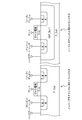
- FIG. 3 is a diagram schematically showing a cross section of the configuration of an enhancement-type normal N-channel MOS transistor and a depletion-type non-doped N-channel MOS transistor.
- a P-type impurity is ion-implanted into a P-type semiconductor substrate to form a P-well (HV (high voltage) P_well), and the N-type source and drain are formed in the P-well.
- the non-doped N-channel MOS transistor impurity implantation for forming a P well is not performed in the channel region, and the impurity concentration of the channel region remains the substrate impurity concentration. Although it depends on the source impurity concentration and the substrate impurity concentration, the non-doped N-channel MOS transistor exhibits depletion characteristics, and the threshold voltage at this time is about ⁇ 0.15V. Further, the substrate bias effect can be obtained by connecting the back gate of the N-channel MOS transistor to the negative power supply terminal (V SS ).
- the negative power supply voltage VSS is applied to the back gate of the N-channel MOS transistor, when the source voltage rises to about 10V, a remarkable substrate bias effect occurs, and the threshold voltage is about ⁇ 0.15V to about +0. . Change to a few volts. As described above, it is important to realize the Rail-to-Rail operation that the threshold voltage changes due to the substrate bias effect in the non-doped N-channel depletion MOS transistor.
- the operational amplifier circuit having both the P-channel differential pair and the N-channel differential pair in FIG. 1 in the differential stage is excellent in the symmetry of the rising / falling characteristics of the output voltage, but has a large chip size.
- the deviation characteristics of the voltage region in the vicinity of the negative power supply voltage VSS and the positive power supply voltage VDD are a problem.
- the operational amplifier circuit having only the depletion type (non-doped) N-channel MOS transistor differential stage of FIG. 2 in the differential stage is excellent in deviation characteristics and chip size, but has a problem in symmetry of rising / falling characteristics.
- the operational amplifier circuits of FIGS. 1 and 2 have advantages and disadvantages, and it is desired to provide an operational amplifier circuit with improved output voltage deviation characteristics and rising / falling characteristics.
- an operational amplifier circuit includes a P-channel differential pair including a pair of P-channel MOS transistors for receiving an input voltage and an N-channel including a pair of depletion-type N-channel MOS transistors for receiving an input voltage.
- An input differential stage including a differential pair and a switch means, and an output unit that outputs an output voltage in response to a current flowing through the P-channel differential pair and the N-channel differential pair.
- the switch means cuts off a bias current flowing through the P-channel differential pair in response to a control signal synchronized with a change in input voltage.
- a display panel driver for driving a data line of a display panel includes a D / A conversion circuit that generates a grayscale voltage corresponding to display data that is digital data, and a grayscale voltage And an operational amplifier circuit for outputting a driving voltage to the data line.
- the operational amplifier circuit includes a P-channel differential pair including a pair of P-channel MOS transistors for receiving a gradation voltage, an N-channel differential pair including a pair of depletion-type N-channel MOS transistors for receiving the gradation voltage, and switching means And an output section that outputs a drive voltage in response to a current flowing through the P-channel differential pair and the N-channel differential pair.
- the switch means cuts off the bias current flowing through the P-channel differential pair in response to the control signal synchronized with the change in the gradation voltage.
- the display device includes a display panel having data lines and a display panel driver for driving the data lines.
- the display panel driver includes a D / A conversion circuit that generates a gradation voltage corresponding to display data that is digital data, and an operational amplifier circuit that outputs a driving voltage corresponding to the gradation voltage to a data line.
- the operational amplifier circuit includes a P-channel differential pair including a pair of P-channel MOS transistors for receiving the gray scale voltage, an N-channel differential pair including a pair of depletion type N-channel MOS transistors for receiving the gray scale voltage, and switching means. And an output section that outputs a drive voltage in response to a current flowing through the P-channel differential pair and the N-channel differential pair.
- the switch means cuts off the bias current flowing through the P-channel differential pair in response to the control signal synchronized with the change in the gradation voltage.
- an operational amplifier circuit in which both the deviation characteristic of the output voltage and the symmetry of the rising / falling characteristic are improved.
- 1 is a circuit diagram showing a configuration of an operational amplifier circuit according to an embodiment of the present invention. It is a circuit diagram which shows the voltage follower using an operational amplifier circuit. When an N-channel differential pair is used for an input differential stage, and when a P-channel differential pair is used for an input differential stage, they are diagrams showing respective output waveforms. It is a circuit diagram explaining the operation
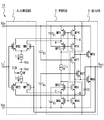
- FIG. 4 is a circuit diagram showing a configuration of the operational amplifier circuit 10 according to the embodiment of the present invention.
- the operational amplifier circuit 10 of the present embodiment is configured as a voltage follower, and generally includes an input differential stage 1, an intermediate stage 2, and an output stage 3.
- the input differential stage 1 includes depletion type N-channel MOS transistors MN1 and MN2 constituting an N-channel differential pair, P-channel MOS transistors MP1 and MP2 constituting a P-channel differential pair, a switch SW, and a constant current.
- Sources I1 and I2 are provided.
- N-channel MOS transistors MN1 and MN2 are depletion type by adding a circle to the symbol indicating the N-channel MOS transistor. .
- N-channel MOS transistors MN1, MN2 has a source are commonly connected, a constant current source I1 is connected between the commonly connected sources and the negative supply voltage V SS terminal (ground terminal).
- the depletion type N channel MOS transistors MN1 and MN2 may be configured as non-doped type N channel MOS transistors shown in FIG.
- the constant current source I1 supplies a bias current to the N-channel MOS transistors MN1 and MN2.
- the sources of the P-channel MOS transistors MP1 and MP2 are connected in common, and a constant current source I2 is connected between the commonly connected source and the terminal of the positive power supply voltage (V DD ).
- the constant current source I2 supplies a bias current to the P channel MOS transistors MP1 and MP2.
- the gates of the N channel MOS transistor MN1 and the P channel MOS transistor MP1 are commonly connected to the output terminal OUT, and the gates of the N channel MOS transistor MN2 and the P channel MOS transistor MP2 are commonly connected to the input terminal In +. Yes.
- a switch SW is connected in series with the constant current source I2 between the common connection source of the P-channel MOS transistors MP1 and MP2 and the terminal of the positive power supply voltage (V DD ).
- the switch SW is Emphasize the differences in the additions.
- the switch SW is turned on in synchronization with the timing at which the input voltage input to the input terminal In + changes, and is turned off after the input voltage is stabilized. As will be described later, such an operation is important for improving both the output voltage deviation characteristic and the rising / falling characteristic.
- the intermediate stage 2 includes P-channel MOS transistors MP3 to MP6, N-channel MOS transistors MN3 to MN6, and a floating current source I3.
- P-channel MOS transistors MP3 to MP6 constitute a folded cascode current mirror that functions as an active load of the N-channel differential pair of input differential stage 1.
- the sources and gates are commonly connected, the commonly-connected sources are connected to the terminal of the positive power supply voltage V DD , and the commonly-connected gate is the P-channel MOS transistor MP3.
- the drain of the P-channel MOS transistor MP5 and the source of the P-channel MOS transistor MP3 are connected to the node A, and the drain of the N-channel differential pair N-channel MOS transistor MN1 is connected to the node A.
- the drain of the P channel MOS transistor MP6 and the source of the P channel MOS transistor MP4 are connected to the node B, and the drain of the N channel MOS transistor MN2 of the N channel differential pair is connected to the node B.
- the gates of the P-channel MOS transistors MP3 and MP4 are commonly connected, and a bias voltage is supplied from the constant voltage source V1 to the commonly connected gates.
- N-channel MOS transistors MN3 to MN6 form a folded cascode current mirror that functions as an active load of the P-channel differential pair of the input differential stage 1.
- N-channel MOS transistors MN5, MN6 the source and between gates are commonly connected, a source connected in common is connected to a terminal of the negative power supply voltage V SS, the commonly connected gates of the N-channel MOS transistor MN3 Connected to the drain.
- the drain of the N channel MOS transistor MN5 and the source of the N channel MOS transistor MN3 are connected to the node C, and the drain of the P channel MOS transistor MP1 of the P channel differential pair is connected to the node C.
- the drain of N-channel MOS transistor MN6 and the source of N-channel MOS transistor MN4 are connected to node D, and the drain of P-channel MOS transistor MP2 of the P-channel differential pair is connected to node D.
- the gates of the N-channel MOS transistors MN3 and MN4 are commonly connected, and a bias voltage is supplied from the constant voltage source V2 to the commonly connected gates.
- the floating current source I3 is connected between the drain of the P-channel MOS transistor MP3 and the drain of the N-channel MOS transistor MN3.
- the output stage 3 includes a P-channel MOS transistors MP7, MP8, and N-channel MOS transistors MN7, MN8, and a phase compensation capacitor C 2.
- P-channel MOS transistor MP7 and N-channel MOS transistor MN7 form a floating current source.
- the P channel MOS transistor MP7 has a source connected to the drain of the P channel MOS transistor MP4 and a drain connected to the drain of the N channel MOS transistor MN4.
- N channel MOS transistor MN7 has a drain connected to the drain of P channel MOS transistor MP4 and a source connected to the drain of N channel MOS transistor MN4. Bias voltages are supplied from constant voltage sources V3 and V4 to the gates of the P-channel MOS transistor MP7 and the N-channel MOS transistor MN7, respectively.
- phase compensation capacitor C 2 between the N-channel MOS transistor MN3 ⁇ node D and N-channel MOS transistor of the folded cascaded current mirror comprised of MN6 MN8 is connected, P-channel MOS Note that no phase compensation capacitor is connected between node B of the folded cascade type current mirror composed of transistors MP3 to MP6 and P-channel MOS transistor MP8. As will be described later, in the operational amplifier circuit 10 of the present embodiment, it is not necessary to provide a phase compensation capacitor between the node B of the folded cascade type current mirror and the P-channel MOS transistor MP8.
- the operational amplifier circuit 10 (FIG. 4) of the present embodiment is decisively different from the conventional operational amplifier circuit of FIG. 1 in that the N channel differential pair (MN1, MN2) is composed of a depletion type N channel MOS transistor. And that the bias current flowing through the P-channel differential pair (MP1, MP2) is on / off controlled by the switch SW.
- the N-channel differential pair (MN1) composed of a depletion type N-channel MOS transistor , MN2) is operated to obtain Rail-to-Rail characteristics.
- the threshold V T of the N channel MOS transistor is ⁇ 0.15V
- the source voltage of the N channel MOS transistors MN1 and MN2 is a positive voltage of about 0.1V when the input voltage is at the level of the negative power supply voltage V SS (GND).
- the constant current source I1 that supplies a bias current to the N-channel differential pair operates at the last minute. That is, the input voltage at the negative supply voltage V SS vicinity, N-channel differential pair operates.
- the gate-source voltage becomes a positive voltage (for example, +0.5 V) due to the influence of the substrate bias effect (the third term of the equation (2) described above).
- the source-drain voltage of the N-channel MOS transistors MN1 and MN2 constituting the N-channel differential pair can be secured to 0.3 V or more, It is possible to operate in the pentode region. Accordingly, the input differential stage operates normally even when the input voltage is near the positive power supply voltage V DD .
- the operational amplifier circuit 10 of this embodiment improves the symmetry of the rise / fall characteristics by temporarily operating both the N-channel differential stage and the P-channel differential stage at the rise and fall. .
- the rising / falling waveform is not so much related to the driving capability of the P-channel MOS transistor constituting the P-channel differential pair, that is, the transistor size. Therefore, the minimum transistor size (or minimum gate width) allowed in the process of integrating the operational amplifier circuit 10 is sufficient for the P-channel MOS transistors MP1 and MP2 of the P-channel differential pair.
- the use of the P-channel MOS transistors MP1 and MP2 having the minimum transistor size as the P-channel differential pair is preferable from the viewpoint of reducing the chip size.
- FIGS. 8A and 8B The results of actually simulating this deviation characteristic are shown in FIGS. 8A and 8B.
- FIG. 8A is a deviation characteristic when there is no switch SW connected to the P-channel differential pair (that is, the conventional operational amplifier circuit of FIG. 1).
- FIG. 8B shows the bias current flowing through the P-channel differential pair as the switch SW. It is a deviation characteristic at the time of interruption
- the operational amplifier circuit 10 of this embodiment can dramatically improve the deviation characteristics as compared with the conventional operational amplifier circuit of FIG. 1.
- the operational amplifier circuit 10 of the present embodiment is more balanced than the conventional operational amplifier circuit of FIG. 1 in terms of the rising and falling characteristics of the output waveform. Have confirmed.
- the configuration of the operational amplifier circuit 10 of this embodiment has an advantage that the number of phase compensation capacitors can be reduced as compared with the conventional operational amplifier circuit of FIG.
- the operational amplifier circuit 10 (FIG. 4) of this embodiment requires only one phase compensation capacitor C 2. Not. This is because in a stable state where the switch (SW) is turned off, the circuit operation is the same as that of the conventional operational amplifier circuit of FIG. 2, and one phase compensation capacitor is sufficient.
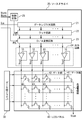
- FIG. 9 is a block diagram showing an example of a schematic configuration of a liquid crystal display device in which the operational amplifier circuit 10 of the present embodiment is applied to the data line driver.
- the liquid crystal display device includes a data line driver 20, a gate line driver 30, and an LCD panel 40.
- the data line driver 20 responds to display data S IN (data indicating the gradation of each pixel of the LCD panel 40) and various control signals supplied from the LCD controller (not shown) and data of the LCD panel 40.
- the line 41 is driven.
- the control signals sent from the LCD controller include a vertical synchronization signal Vsync, a horizontal synchronization signal Hsync, and a polarity signal POL.
- the polarity signal POL is a signal that specifies the polarity of the drive voltage that the data line driver 20 outputs to each data line 41.
- the polarity of the driving voltage is defined with reference to the potential of the common electrode of the liquid crystal display panel 40 (common potential V COM ).
- the gate line driver 30 drives the gate line 42 of the LCD panel 40.
- the LCD panel 40 includes a pixel 43 at each position where the data line 41 and the gate line 42 intersect, and displays an image corresponding to the display data.
- the data line driver 20 includes a data register circuit 21, a latch circuit 22, a D / A conversion circuit 23, an output circuit 24, and a control circuit 25.
- Data register circuit 21 sequentially receives the display data S IN to be transferred from the LCD controller (not shown) serially outputs in parallel.
- Latch circuit 22 latches the display data S IN from the data register circuit 21 in response to a strobe signal STB supplied from the control circuit 25.
- D / A converter circuit 23 performs D / A conversion on the display data S IN supplied from the latch circuit 22, generates the gray voltages corresponding to the display data S IN.
- the polarity of the output gradation voltage is selected according to the polarity signal POL.
- the output circuit 24 performs impedance conversion on the gradation voltage received from the D / A conversion circuit 23 to generate a drive voltage supplied to the data line 41.
- the operational amplifier circuit 10 described above is used in the output circuit 24. That is, the operational amplifier circuit 10 receives the gradation voltage from the D / A conversion circuit 23 as an input voltage, and outputs the drive voltage supplied to the data line 41 as an output voltage.
- the operational amplifier circuit 10 of the output circuit 24 changes.
- the input voltage changes. That is, if the switch SW of the input differential stage 1 of the operational amplifier circuit 10 is controlled according to the assertion of the strobe signal STB, the switch SW can be selectively turned on only when the output voltage rises or falls. .
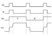
- FIG. 10 is a timing chart showing an example of control of the switch SW.
- the switch SW for operating the P-channel differential pair is turned on for a certain period in synchronization with the rising edge of the strobe signal STB.
- both the P-channel differential pair and the N-channel differential pair are operating only while the switch SW is on.
- the strobe signal STB is a signal synchronized with the start of each horizontal period.
- the strobe signal STB can be generated by delaying the horizontal synchronization signal Hsync by several clocks. Note that the period during which the switch SW is on does not have to be the same as the pulse width of the strobe signal STB, and can be arbitrarily adjusted as long as the switch SW is turned off after the output voltage is stabilized.
- the influence of the on / off of the switch SW by switching the on / off of the switch SW gently. That is, when the switch SW is turned off in the operation of FIG. 10, the influence of noise on the output waveform can be reduced by controlling so that the bias current of the P-channel differential pair gradually decreases. For example, when a P-channel MOS transistor is used as the switch SW, if the gate voltage of the P-channel MOS transistor is gradually pulled up from the Low level to the High level, the influence of ON / OFF of the switch SW can be reduced.
- the operational amplifier circuit 10 of the present embodiment controls the output voltage by controlling both the P-channel differential pair and the N-channel differential pair to operate only during the period when the output transitions. It is possible to improve the balance between the rising characteristic and the falling characteristic of.
- the operational amplifier circuit 10 of this embodiment controls the deviation characteristic by controlling only the N-channel differential pair composed of the depletion-type N-channel MOS transistor after the output is stabilized. Can be improved.
- the operational amplifier circuit 10 of this embodiment can halve the number of phase compensation capacitors compared to the conventional operational amplifier circuit of FIG.
- the effect of the phase compensation capacitance on the chip size is large, and the fact that the phase compensation capacitance is halved leads to a reduction in the chip size. This is preferable in that the cost can be suppressed.
- FIG. 11 is a circuit diagram showing a modification of the operational amplifier circuit of the present invention. 4 is derived from the conventional operational amplifier circuit of FIG. 1, whereas the operational amplifier circuit of FIG. 11 is derived from the conventional operational amplifier circuit of FIG. Specifically, the operational amplifier circuit 10A of FIG. 11 has a configuration in which an intermediate stage of the conventional operational amplifier circuit of FIG. 2 is connected to the input differential stage 1 of the operational amplifier circuit 10 of FIG.
- the intermediate stage 2A of the operational amplifier circuit 10A of FIG. 11 includes a Widdler type current mirror composed of N channel MOS transistors MN5 and MN6 instead of the folded cascode type current mirror composed of N channel MOS transistors. .
- the sources and gates of the N-channel MOS transistors MN5 and MN6 are commonly connected, the commonly connected source is the terminal of the negative power supply voltage VSS , and the commonly connected gate is the drain of the N-channel MOS transistor MN5. It is connected to the.
- the drain of N channel MOS transistor MN5 is connected to node C, and the drain of N channel MOS transistor MN6 is connected to node D.
- the node C is a node to which the drain of the P-channel MOS transistor MP1 of the input differential stage 1 is connected
- the node D is a node to which the drain of the P-channel MOS transistor MP2 is connected.
- the basic operation of the operational amplifier circuit 10A shown in FIG. 11 is the same as that of the operational amplifier circuit 10 shown in FIG. 4, and the timing control relationship of the switch SW is also the same.
- the operational amplifier circuit 10A of FIG. 11 differs from the operational amplifier circuit 10 of FIG. 4 only in the active load of the P-channel differential pair provided in the intermediate stage 2A. That is, in the operational amplifier circuit 10 of FIG. 4, a folded cascode current mirror composed of an N-channel MOS transistor is used as an active load of the P-channel differential pair, whereas the operational amplifier circuit 10A of FIG. So, a simple Widdler current mirror is used.
- a Widoler type current mirror (not a folded cascode type) may be used as in the operational amplifier circuit 10A of FIG.
- the active load connected to the P-channel differential pair is a Widdler type. Therefore, as in the operational amplifier circuit 10 shown in FIG.
- the voltage source V2 is not necessary. This has the advantage that the circuit configuration is simplified and the power consumption can be reduced. Further, by using a Widdler type current mirror instead of the folded cascode type current mirror, there is an effect that the number of elements used can be reduced and the chip size can be reduced. This leads to a cost reduction effect.
- the output stage 3 (MN7, MN8, MP7, MP8) can be changed in any circuit.
- the half of the voltage V DD / 2 is supplied to the source of the N-channel MOS transistor MN8 of the output stage 3 instead of the power supply voltage V DD.
- a voltage V DD / 2 that is half of the power supply voltage V DD may be supplied to the source of the P-channel MOS transistor MP8 in the output stage 3.
- a circuit configuration in which only the output stage supplies power at a reduced voltage is disclosed in, for example, Japanese Unexamined Patent Application Publication No. 2009-244830, and the present invention can also be applied to such a circuit.
- a configuration in which the switch SW is provided between the constant current source I2 and the terminal of the positive power supply voltage V DD is illustrated, but the position of the switch SW is the same as that of the constant current source I2 and the positive power supply voltage. It is not limited between the terminals of the voltage V DD and can be changed to various positions where the bias current can be cut off.
- a switch SW may be provided between the common connection source of the P-channel MOS transistors MP1 and MP2 and the constant current source I2.
- switches may be provided between the node C of the intermediate stage 2 and the drain of the P-channel MOS transistor MP1, and at two places, the node D of the intermediate stage 2 and the drain of the P-channel MOS transistor MP2.
Landscapes
- Engineering & Computer Science (AREA)
- Power Engineering (AREA)
- Amplifiers (AREA)
Abstract
演算増幅器回路が、入力電圧を受け取る一対のPチャネルMOSトランジスタを含むPチャネル差動対と、入力電圧を受け取る一対のディプレッション型のNチャネルMOSトランジスタを含むNチャネル差動対と、スイッチ手段とを備える入力差動段と、Pチャネル差動対とNチャネル差動対に流れる電流に応答して出力電圧を出力する出力部とを具備する。スイッチ手段は、入力電圧の変化に同期した制御信号に応答してPチャネル差動対を流れるバイアス電流を遮断する。
Description
本発明は、演算増幅器回路並びにそれを用いた表示パネルドライバ及び表示装置に関し、特に、演算増幅器回路の過渡特性の改善に関する。
最近の液晶表示装置その他のパネル表示装置において、表示画像の画質に顕著に影響を及ぼす回路の一つが出力アンプとして使用される演算増幅器回路である。表示画像の画質の向上のためには、例えば、偏差特性や、出力信号の立ち上がり及び立ち下がりの対称性が良好であることが望ましく、このような特性を持つ演算増幅器回路の提供が望まれる。
パネル表示装置の出力アンプとして、入力電圧及び出力電圧のいずれもが負電源電圧から正電源電圧までの任意の電圧をとることを許容する、いわゆるRail-to-Rail動作に対応した演算増幅器回路が使用されることがある。Rail-to-Rail動作を実現するための回路構成としては、2つが知られている:一つは、入力差動段にPチャネルMOSトランジスタの差動対(「Pチャネル差動対」ともいう。)とNチャネルMOSトランジスタの差動対(「Nチャネル差動対」ともいう。)の両方を設ける回路構成であり、もう一つは、ディプレッションタイプのNチャネルMOSトランジスタの差動対のみを設ける構成である。
図1は、入力差動段にPチャネルMOSトランジスタの差動対とNチャネルMOSトランジスタ差動対の両方を設ける、典型的なRail-to-Railアンプの回路構成を示す回路図である。図1のような回路構成は、例えば、米国特許第5,311,145号に開示されており、この特許文献以外にもCMOSアナログ回路の教科書や著名な文献等に、参考回路として記載されている。図1を参照すると、この演算増幅器の回路構成は、入力差動段(初段)、中間段及び最終段と大きく3つに分けられる。
図1を参照すると、入力差動段は、NチャネルMOSトランジスタMN1、MN2で構成されたNチャネル差動対と、PチャネルMOSトランジスタMP1、MP2で構成されたPチャネル差動対とを備えている。NチャネルMOSトランジスタMN1、MN2は、ソースが共通に接続され、共通接続されたソースと負電源電圧VSSの端子(接地端子)との間に、定電流源I1が接続されている。一方、PチャネルMOSトランジスタMP1、MP2は、ソースが共通接続され、共通接続されたソースと正電源電圧VDDの電源端子との間に、定電流源I2が接続されている。PチャネルMOSトランジスタMP1のゲートとNチャネルMOSトランジスタMN1のゲートは、入力端子IN-に共通接続されており、PチャネルMOSトランジスタMP2のゲートとNチャネルMOSトランジスタMN2のゲートは、入力端子IN+に共通接続されている。
中間段は、能動負荷として機能する2つのフォールデッドカスコード型カレントミラーと、浮遊電流源I3とを有する。PチャネルMOSトランジスタMP3~MP6は、第1のフォールデッドカスコード型カレントミラーを構成しており、NチャネルMOSトランジスタMN3~MN6は、第2のフォールデッドカスコード型カレントミラーを構成している。定電圧源V1は、PチャネルMOSトランジスタMP5、MP6に電圧バイアスを供給し、定電圧源V2は、NチャネルMOSトランジスタMN5、MN6に電圧バイアスを供給している。中間段のノードAは差動段のNチャネルMOSトランジスタMN1のドレインに接続され、ノードBは、NチャネルMOSトランジスタMN2のドレインに接続されている。同様に、中間段のノードCは差動段のPチャネルMOSトランジスタMP1のドレインに接続され、ノードDは、PチャネルMOSトランジスタMP2のドレインに接続されている。
最終段は、定電圧源V3、V4で制御されたAB級増幅器として構成されており、NチャネルMOSトランジスタMN7、MN8とPチャネルMOSトランジスタMP7、MP8とを備えている。PチャネルMOSトランジスタMP7とNチャネルMOSトランジスタMN7は、浮遊定電流源(Floating Current Source)として機能する。PチャネルMOSトランジスタMP7のソースとNチャネルMOSトランジスタMN7のドレインはPチャネルMOSトランジスタMP6のドレインに接続され、PチャネルMOSトランジスタMP7のドレインとNチャネルMOSトランジスタMN7のソースはNチャネルMOSトランジスタMN6のドレインに接続されている。PチャネルMOSトランジスタMP8は、ソースが正電源電圧VDDの電源端子に接続され、ゲートがPチャネルMOSトランジスタMP7のソースに接続され、ドレインが出力端子OUTに接続されている出力トランジスタである。NチャネルMOSトランジスタMN8は、ソースが負電源電圧VSSの電源端子に接続され、ゲートがNチャネルMOSトランジスタMN7のソースに接続され、ドレインが出力端子OUTに接続されている出力トランジスタである。位相補償容量C1は、一端が中間段のノードBに接続され、他端が出力端子OUTに接続されている。位相補償容量C2は、一端が中間段のノードDに接続され、他端が出力端子OUTに接続されている。このAB級増幅器のアイドリング電流は、浮遊定電流源(MP7、MN7)を流れる電流と第3と第4の定電圧源から供給される電圧バイアスで決定される。
図1の演算増幅器回路は、以下のように動作してRail-to-Rail動作を実現している。入力電圧が低い時には、Pチャネル差動対(MP1、MP2)が動作する。反対に入力電圧が高い時にはNチャネル差動対(MN1、MN2)が動作する。その中間の入力電圧では、Pチャネル差動対(MP1、MP2)及びNチャネル差動対(MN1、MN2)がともに動作する。すなわち、負電源電圧VSS近傍の動作においては、Pチャネル差動対(MP1、MP2)のみが動作し、Nチャネル差動対(MN1、MN2)は動作しない。これは、NチャネルMOSトランジスタは、一般的には、エンハンスメントタイプのトランジスタ特性であるため、動作するためには、ゲート-ソース間電圧がトランジスタの閾値電圧(VT)よりも高くなる必要があるためである。しかし、入力電圧が負電源電圧VSS近傍の電圧である場合、すなわち、入力差動トランジスタのゲート電圧が0V近辺である場合には、そのソース電位も0V近辺となり、Nチャネル差動対(MN1、MN2)が動作しないことが理解できる。また、入力電圧が正電源電圧VDD近傍の電圧である場合、すなわち、入力差動トランジスタのゲート電圧がVDD近辺である場合には、そのソース電位も正電源電圧VDD近辺となり、Pチャネル差動対(MP1、MP2)が動作しないことが理解できる。入力電圧が約VTN~VDD-VTP(VTN:NチャネルMOSトランジスタの閾値電圧、VTP:PチャネルMOSトランジスタの閾値電圧)の時は、Pチャネル差動段(MP1、MP2)、Nチャネル差動段(MN1、MN2)の両方が動作する。したがって、図1の演算増幅器回路は、負電源電圧VSSから正電源電圧VDDの全範囲で動作可能である。
一方、図2は、ディプレッション型のNチャネルMOSトランジスタの差動対のみを設けた演算増幅器回路の構成を示す回路図である。このような構成は、例えば、特開2007-202127号公報に開示されている。図2を参照すると、入力差動段は、ソースが共通接続され、各々のゲートが入力端子In-、In+に接続されたディプレッション型のNチャネルMOSトランジスタMN1、MN2と、NチャネルMOSトランジスタMN1、MN2の共通接続されたソースと負電源電圧VSSの電源端子との間に接続された定電流源I1を備えている。ここで、図2においては、NチャネルMOSトランジスタMN1、MN2がディプレッション型であることを明示するために、NチャネルMOSトランジスタを示す記号に丸が付されていることに留意されたい。NチャネルMOSトランジスタMN1、MN2のバックゲートは、負電源端子(VSS)に接続されている。
中間段は、浮遊電流源I3と、NチャネルMOSトランジスタMN3、MN4と、PチャネルMOSトランジスタMP3、MP4、MP5、MP6、MP7とを備えている。NチャネルMOSトランジスタMN3、MN4はカレントミラーを構成しており、また、PチャネルMOSトランジスタMP3、MP4、MP5、MP6は、フォールデッドカスコード型カレントミラーを構成している。定電圧源V1は、PチャネルMOSトランジスタMP5、MP6に電圧バイアスを供給している。
最終段は、NチャネルMOSトランジスタMN7、MN8とPチャネルMOSトランジスタMP7、MP8とを備えている。PチャネルMOSトランジスタMP7とNチャネルMOSトランジスタMN7は、浮遊定電流源(Floating Current Source)として機能する。NチャネルMOSトランジスタMN8、PチャネルMOSトランジスタMP8は、出力端子OUTを駆動する出力トランジスタである。最終段は、更に、位相補償容量としてC2を備えている。
図2の演算増幅器回路は、差動対にディプレッション型Nチャネルトランジスタを用い、その能動負荷としてフォールデッドカスコード型カレントミラーを用いることで、Rail-to-Rail動作を実現している。以下、この詳細な説明を行う。
PチャネルMOSトランジスタMP3、MP4の共通接続されたゲートとPチャネルMOSトランジスタMP5のドレインを共通接続して、フォールデッドカスコード型カレントミラーの入力端子が構成されている。そして、PチャネルMOSトランジスタMP3、MP4の共通接続されたソースが、フォールデッドカスコード型カレントミラーの共通端子となり、PチャネルMOSトランジスタMP6のドレインが、カスコードカレントミラー回路の出力端子となる。このフォールデッドカスコード型カレントミラーは、入力差動段の出力に接続された能動負荷の働きをする。一般のカスコード型カレントミラーを通常の能動負荷として動作させる時は、カスコード型カレントミラーの入力端子と出力端子を使用するが、フォールデッドカスコード型カレントミラーの場合は、縦積みされたカレントミラーの中間ノード、すなわち、PチャネルMOSトランジスタMP3、MP4の各々のドレインに差動段の出力が接続される。これにより、以下に詳述されるように、入力差動段の入力電圧範囲を広くすることが可能となる。図2のように構成された演算増幅器回路は、入力電圧範囲が、ほぼ負電源電圧VSSからほぼ正電源電圧VDDまでとなり、いわゆるRail-to-Rail動作が可能な回路となる。このように、Nチャネルディプレッション型MOSトランジスタの差動段と、フォールデッドカスコード型カレントミラーとを組み合わせることにより、負電源電圧VSSから正電源電圧VDDまでの全電源範囲の入力電圧で動作することを、図2を参照して説明する。
まず、1つの差動対でRail-to-Rail動作が実現できる理由について説明する。図2の演算増幅器回路において、反転入力端子In-を出力端子OUTに接続する、いわゆるボルテージフォロワ接続がなされているとして、正転入力端子In+に入力される電圧をVinとすると、入力できる電圧範囲は、次式(1)で与えられる:
 ここで、VDS(sat)(MP1/2)は、Pチャンネル型MOSトランジスタMP1、MP2の飽和点でのドレイン-ソース間電圧であり、VDS(sat)(MN1/2)はNチャンネル型MOSトランジスタMN1/2の飽和点でのドレイン-ソース間電圧であり、VDS(sat)(I2)は定電流源I2を構成するNチャンネル型MOSトランジスタの飽和点でのドレイン-ソース間電圧(5極管領域で動作するぎりぎりの電圧)であり、VGS(MN1/2)はNチャンネル型MOSトランジスタMN1/2のゲート-ソース間電圧である。
また、MOSトランジスタのゲート-ソース間電圧VGSは、基板バイアス効果を考慮すると、次式(2)で与えられる:
 ただし、μは移動度であり、C0は単位面積当たりのゲート絶縁膜容量(F/cm2)であり、ε0は、自由空間の誘電率(8.86×10-14F/cm)であり、εsは、半導体の比誘電率(3.9)であり、qは電子の電荷量(1.6×10-12C)であり、VT0は、基板バイアスVBが0Vである場合の閾値電圧であり、IDは、ドレイン-ソース間電流であり、βは利得係数であり、γは基板バイアス効果を表す係数である。
仮にNチャンネルMOSトランジスタの閾値が-0.15Vであり、ディプレッション特性を示すとする。入力Vinが0V近辺の時は、NチャネルMOSトランジスタMN1、MN2の共通ソースとバックゲート(この場合は、サブストレート)間の電圧は、0.1V程度で、基板バイアス効果がほとんどない。従って、式(2)を式(1)の右辺に代入すると、VDS(sat)(I1)が0.1Vであるとして、VGS(MN1/2)が約-0.1Vになるから、次式が成立する:
 これは、入力電圧Vinの許容される最低電圧がほぼ0V(VSS)であることを意味している。
一方、正電源電圧VDD近辺の入力電圧が入力された場合には、差動段のNチャネルMOSトランジスタMN1、MN2の共通ソースとバックゲートの間に正電源電圧VDD近くの電圧がかかる。LCDデータ線ドライバの場合は、正電源電圧VDDが10V以上になり、式(2)の第3項のバックゲート効果により、ゲート-ソース間電圧は約+0.5Vにもなる。これを式(1)の左辺に代入すると、
 となり、入力電圧の許容される最高電圧がほぼ正電源電圧VDDであることがわかる。
このように、MOSトランジスタのバックゲート-ソース間の電圧の増加による顕著な基板バイアス効果の影響と、入力差動段の出力を(通常の能動負荷となるカレントミラー回路で受けるのではなく)フォールデッドカスコード型カレントミラーで受けることにより、ディプレッション型のトランジスタを使った差動段でも、入力電圧範囲をVDDまで拡大することが可能となる。
中間段と出力段の動作に関しては、前述の図1の演算増幅器回路の場合とほぼ同じなので、その説明を省略する。
特開2007-202127号公報における演算増幅器回路では、差動段のNチャンネル型ディプレッションMOSトランジスタをノンドープトランジスタ構造で実現している。以下、このノンドープ構造のディプレッション型NチャネルMOSトランジスタについて説明する。図3は、エンハンスメント型の通常のNチャネルMOSトランジスタと、ディプレッション型のノンドープ構造のNチャネルMOSトランジスタの構成の断面を模式的に示す図である。右側の通常のNチャネルMOSトランジスタにおいては、P型の半導体基板にP型の不純物をイオン注入してPウェル(HV(high voltage)P_well)が形成され、そのPウェルにN型のソース及びドレインが形成される。一方、ノンドープ型のNチャネルMOSトランジスタにおいては、チャネル領域に対してPウェルを形成するための不純物注入を行わず、チャネル領域の不純物濃度は基板不純物濃度のままである。ソース不純物濃度と基板不純物濃度にもよるが、ノンドープ型のNチャネルMOSトランジスタは、ディプレッション特性を示し、このときの閾値電圧は、約―0.15Vとなる。さらに、NチャネルMOSトランジスタのバックゲートを負電源端子(VSS)に接続することで、基板バイアス効果が得られる。NチャネルMOSトランジスタのバックゲートには負電源電圧VSSを印加しているので、ソース電圧が10V程度に上昇した場合、顕著な基板バイアス効果が生じ、閾値電圧が約-0.15Vから約+0.数Vに変化する。上述のように、ノンドープ型のNチャネルディプレッションMOSトランジスタにおいて基板バイアス効果によって閾値電圧が変化することが、Rail-to-Rail動作を実現する上で重要である。
しかし、図1のPチャネル差動対とNチャネル差動対の両方を差動段に備えた演算増幅器回路は、出力電圧の立ち上がり/立ち下がり特性の対称性には優れるが、チップサイズが大きくなり、更に負電源電圧VSS及び正電源電圧VDD近辺の電圧領域の偏差特性が問題である。一方、図2のディプレッション型(ノンドープ型)のNチャンネルMOSトランジスタ差動段のみを差動段に備えた演算増幅器回路は偏差特性とチップサイズに優れるが、立ち上がり/立ち下がり特性の対称性に問題がある。図1、図2の演算増幅器回路は一長一短であり、出力電圧の偏差特性と立ち上がり/立ち下がり特性の両方が向上された演算増幅器回路の提供が望まれている。
本発明の一の観点においては、演算増幅器回路が、入力電圧を受け取る一対のPチャネルMOSトランジスタを含むPチャネル差動対と、入力電圧を受け取る一対のディプレッション型のNチャネルMOSトランジスタを含むNチャネル差動対と、スイッチ手段とを備える入力差動段と、Pチャネル差動対とNチャネル差動対に流れる電流に応答して出力電圧を出力する出力部とを具備する。スイッチ手段は、入力電圧の変化に同期した制御信号に応答してPチャネル差動対を流れるバイアス電流を遮断する。
本発明の他の観点では、表示パネルのデータ線を駆動するための表示パネルドライバが、デジタルデータである表示データに対応する階調電圧を生成するD/A変換回路と、階調電圧に対応する駆動電圧をデータ線に出力する演算増幅器回路とを備えている。演算増幅器回路は、階調電圧を受け取る一対のPチャネルMOSトランジスタを含むPチャネル差動対と、階調電圧を受け取る一対のディプレッション型のNチャネルMOSトランジスタを含むNチャネル差動対と、スイッチ手段とを備える入力差動段と、Pチャネル差動対とNチャネル差動対に流れる電流に応答して駆動電圧を出力する出力部とを具備している。スイッチ手段は、階調電圧の変化に同期した制御信号に応答してPチャネル差動対を流れるバイアス電流を遮断する。
本発明の更に他の観点では、表示装置が、データ線を備える表示パネルと、データ線を駆動する表示パネルドライバとを具備する。表示パネルドライバは、デジタルデータである表示データに対応する階調電圧を生成するD/A変換回路と、階調電圧に対応する駆動電圧をデータ線に出力する演算増幅器回路とを備えている。演算増幅器回路は、階調電圧を受け取る一対のPチャネルMOSトランジスタを含むPチャネル差動対と、階調電圧を受け取る一対のディプレッション型のNチャネルMOSトランジスタを含むNチャネル差動対と、スイッチ手段とを備える入力差動段と、Pチャネル差動対とNチャネル差動対に流れる電流に応答して駆動電圧を出力する出力部とを具備する。スイッチ手段は、階調電圧の変化に同期した制御信号に応答してPチャネル差動対を流れるバイアス電流を遮断する。
本発明によれば、出力電圧の偏差特性と立ち上がり/立ち下がり特性の対称性の両方が向上された演算増幅器回路が提供される。
(演算増幅器回路の回路構成)
図4は、本発明の一実施形態の演算増幅器回路10の構成を示す回路図である。本実施形態の演算増幅器回路10は、ボルテッジフォロアとして構成されており、概略的には、入力差動段1と、中間段2と、出力段3とで構成される。
図4は、本発明の一実施形態の演算増幅器回路10の構成を示す回路図である。本実施形態の演算増幅器回路10は、ボルテッジフォロアとして構成されており、概略的には、入力差動段1と、中間段2と、出力段3とで構成される。
入力差動段1は、Nチャネル差動対を構成するディプレッション型のNチャネルMOSトランジスタMN1、MN2と、Pチャネル差動対を構成するPチャネルMOSトランジスタMP1、MP2と、スイッチSWと、定電流源I1、I2とを備えている。ここで、図4においても図2と同様に、NチャネルMOSトランジスタを示す記号に丸を付すことにより、NチャネルMOSトランジスタMN1、MN2がディプレッション型であることを明示されていることに留意されたい。NチャネルMOSトランジスタMN1、MN2は、そのソースが共通接続されており、共通接続されたソースと負電源電圧VSSの端子(接地端子)の間に定電流源I1が接続されている。ディプレッション型であるNチャネルMOSトランジスタMN1、MN2は、図3に図示されている、ノンドープ型のNチャネルMOSトランジスタとして構成されてもよい。定電流源I1は、NチャネルMOSトランジスタMN1、MN2にバイアス電流を供給する。PチャネルMOSトランジスタMP1、MP2も同様に、そのソースが共通接続されており、共通接続されたソースと正電源電圧(VDD)の端子の間に定電流源I2が接続されている。定電流源I2は、PチャネルMOSトランジスタMP1、MP2にバイアス電流を供給する。NチャネルMOSトランジスタMN1と、PチャネルMOSトランジスタMP1のゲートは、出力端子OUTに共通接続されており、NチャネルMOSトランジスタMN2とPチャネルMOSトランジスタMP2のゲートは、入力端子In+に共通接続されている。加えて、PチャネルMOSトランジスタMP1、MP2の共通接続ソースと正電源電圧(VDD)の端子の間に、定電流源I2と直列にスイッチSWが、接続されている。
図4の演算増幅器回路の入力差動段1の構成は、図1の演算増幅器回路の入力差動段と比較すると、NチャネルMOSトランジスタMN1、MN2がディプレッション型である点、及び、スイッチSWが追加されている点で異なることを強調しておく。スイッチSWは、入力端子In+に入力される入力電圧が変化するタイミングに同期してオンされ、入力電圧が安定した後にオフされる。後述されるように、このような動作が、出力電圧の偏差特性と立ち上がり/立ち下がり特性の両方を向上するために重要である。
中間段2は、PチャネルMOSトランジスタMP3~MP6と、NチャネルMOSトランジスタMN3~MN6と、浮遊電流源I3とを備えている。
PチャネルMOSトランジスタMP3~MP6は、入力差動段1のNチャネル差動対の能動負荷として機能するフォールデッドカスコート型カレントミラーを構成している。PチャネルMOSトランジスタMP5、MP6は、ソース同士及びゲート同士が共通接続されており、共通接続されたソースは正電源電圧VDDの端子に接続され、共通接続されたゲートはPチャネルMOSトランジスタMP3のドレインに接続されている。PチャネルMOSトランジスタMP5のドレインとPチャネルMOSトランジスタMP3のソースは、ノードAに接続されており、そのノードAにNチャネル差動対のNチャネルMOSトランジスタMN1のドレインが接続される。同様に、PチャネルMOSトランジスタMP6のドレインとPチャネルMOSトランジスタMP4のソースは、ノードBに接続されており、そのノードBにNチャネル差動対のNチャネルMOSトランジスタMN2のドレインが接続される。PチャネルMOSトランジスタMP3、MP4は、ゲート同士が共通接続されており、その共通接続されたゲートには、定電圧源V1からバイアス電圧が供給されている。
同様に、NチャネルMOSトランジスタMN3~MN6は、入力差動段1のPチャネル差動対の能動負荷として機能するフォールデッドカスコート型カレントミラーを構成している。NチャネルMOSトランジスタMN5、MN6は、ソース同士及びゲート同士が共通接続されており、共通接続されたソースは負電源電圧VSSの端子に接続され、共通接続されたゲートはNチャネルMOSトランジスタMN3のドレインに接続されている。NチャネルMOSトランジスタMN5のドレインとNチャネルMOSトランジスタMN3のソースは、ノードCに接続されており、そのノードCにPチャネル差動対のPチャネルMOSトランジスタMP1のドレインが接続される。同様に、NチャネルMOSトランジスタMN6のドレインとNチャネルMOSトランジスタMN4のソースは、ノードDに接続されており、そのノードDにPチャネル差動対のPチャネルMOSトランジスタMP2のドレインが接続される。NチャネルMOSトランジスタMN3、MN4は、ゲート同士が共通接続されており、その共通接続されたゲートには、定電圧源V2からバイアス電圧が供給されている。浮遊電流源I3は、PチャネルMOSトランジスタMP3のドレインとNチャネルMOSトランジスタMN3のドレインの間に接続される。
出力段3は、PチャネルMOSトランジスタMP7、MP8と、NチャネルMOSトランジスタMN7、MN8と、位相補償容量C2とを備えている。PチャネルMOSトランジスタMP7、NチャネルMOSトランジスタMN7は、浮遊電流源を構成している。PチャネルMOSトランジスタMP7は、ソースがPチャネルMOSトランジスタMP4のドレインに接続され、ドレインがNチャネルMOSトランジスタMN4のドレインに接続されている。NチャネルMOSトランジスタMN7は、ドレインがPチャネルMOSトランジスタMP4のドレインに接続され、ソースがNチャネルMOSトランジスタMN4のドレインに接続されている。PチャネルMOSトランジスタMP7、NチャネルMOSトランジスタMN7のゲートには、それぞれ、定電圧源V3、V4からバイアス電圧が供給される。
出力段3において、NチャネルMOSトランジスタMN3~MN6で構成されたフォールデッドカスケード型カレントミラーのノードDとNチャネルMOSトランジスタMN8の間に位相補償容量C2が接続されている一方で、PチャネルMOSトランジスタMP3~MP6で構成されたフォールデッドカスケード型カレントミラーのノードBとPチャネルMOSトランジスタMP8の間には位相補償容量が接続されていないことに留意されたい。後述のように、本実施形態の演算増幅器回路10では、フォールデッドカスケード型カレントミラーのノードBとPチャネルMOSトランジスタMP8の間に位相補償容量を設ける必要がない。
(演算増幅器回路の定常動作)
以下、本実施形態の演算増幅器回路10の動作について詳細に説明する。本実施形態の演算増幅器回路10(図4)が、図1の従来の演算増幅器回路と決定的に異なる点は、Nチャネル差動対(MN1、MN2)がディプレッション型のNチャンネルMOSトランジスタで構成されていることと、Pチャネル差動対(MP1、MP2)を流れるバイアス電流がスイッチSWでオン/オフ制御される回路構成になっていることである。
以下、本実施形態の演算増幅器回路10の動作について詳細に説明する。本実施形態の演算増幅器回路10(図4)が、図1の従来の演算増幅器回路と決定的に異なる点は、Nチャネル差動対(MN1、MN2)がディプレッション型のNチャンネルMOSトランジスタで構成されていることと、Pチャネル差動対(MP1、MP2)を流れるバイアス電流がスイッチSWでオン/オフ制御される回路構成になっていることである。
スイッチSWがオフした状態、即ち、Pチャネル差動対(MP1、MP2)を流れるバイアス電流が遮断されている状態においても、ディプレッション型のNチャンネルMOSトランジスタで構成されたNチャネル差動対(MN1、MN2)を動作させることでRail-to-Rail特性が得られる。これは、図2の回路を参照して説明した通りである。すなわち、NチャネルMOSトランジスタの閾値VTが-0.15Vと仮定すると、入力電圧が負電源電圧VSS(GND)レベルの時にはNチャネルMOSトランジスタMN1、MN2のソース電圧が約0.1Vの正電圧となり、Nチャネル差動対にバイアス電流を供給する定電流源I1がぎりぎり動作する。即ち、入力電圧が負電源電圧VSS近傍でも、Nチャネル差動対が動作する。
一方、入力電圧が正電源電圧VDDの場合には、基板バイアス効果の影響(上述した式(2)の第3項)でゲート-ソース間電圧が正の電圧(例えば+0.5V)となる。このことと中間段2でフォールデッドカスコード型カレントミラーが使用されている効果により、Nチャネル差動対を構成するNチャネルMOSトランジスタMN1、MN2のソース-ドレイン間電圧が0.3V以上確保でき、5極管領域で動作させることが可能になる。従って、入力電圧が正電源電圧VDD近傍でも入力差動段として正常な動作をする。以上のことより、入力電圧が負電源電圧VSS(GND)から正電源電圧VDDの全範囲において正常に動作する、いわゆるRail-to-Rail動作が可能となる。従って、定常状態の動作においては、Pチャネル差動対がオフした状態でも、何ら問題ない。
(演算増幅器回路の過渡特性)
しかしながら、入力電圧が過渡的に変化する場合には、Nチャネル差動対(MN1、MN2)のみを動作させると、出力電圧の立ち上がり/立ち下がり特性(立ち上がり時間tr、立ち下がり時間tf)が対称にならないという問題が発生する。このことはNチャネル差動対の共通接続されたソースと基板間に生じる寄生容量によるものである。以下にその説明を行う。
しかしながら、入力電圧が過渡的に変化する場合には、Nチャネル差動対(MN1、MN2)のみを動作させると、出力電圧の立ち上がり/立ち下がり特性(立ち上がり時間tr、立ち下がり時間tf)が対称にならないという問題が発生する。このことはNチャネル差動対の共通接続されたソースと基板間に生じる寄生容量によるものである。以下にその説明を行う。
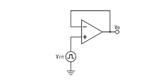
まず、図5Aを参照して、入力差動段にNチャネル差動対のみを使用した演算増幅器回路及びPチャネル差動対のみを使用した演算増幅器回路にパルス入力を入れる場合について議論する。当該演算増幅器回路は、ボルテージフォロワとして構成されているものとする。図5Bに図示されているように、Nチャネル差動対のみが入力差動段として使用される場合に、入力電圧が立ちあげられると、出力電圧は、瞬時にステップ状に立ち上がり、その後、比較的に速いスルーレート(SR+)で出力電圧が上昇する。一方、立ち下がり時は、遅いスルーレート(SR-)で出力電圧がだらだら低下する。Pチャンネル差動対のみが使用される場合は全くこの逆で、立ち上がり時は出力電圧がだらだら上がり、立ち下がり時は出力電圧が瞬時にステップ状に立ち下がり、その後、比較的に速いスルーレートで立ち下がる。
上述した現象は、初段の共通ソースと定電流源に付加される寄生容量(Cs:input tail
capacitance)の影響によるものでありIEEE J.Solid-State Circuits, vol.SC-9,
PP314-332, Dec.1974に詳細が示されている。以下では、この文献に従って、図6のNチャネル差動対を有する差動増幅器回路を例にとって解析を行う。
capacitance)の影響によるものでありIEEE J.Solid-State Circuits, vol.SC-9,
PP314-332, Dec.1974に詳細が示されている。以下では、この文献に従って、図6のNチャネル差動対を有する差動増幅器回路を例にとって解析を行う。
(1)立ち下がり波形解析
まず、立ち下がり波形の解析を行う。前述したように入力差動段(M1、M2)の共通ソースと定電流源(電流値2I1)に付加される寄生容量Csが立ち下がり波形に影響するので、この寄生容量Csを加味して解析を行う必要がある。立ち下がり時はNチャネルMOSトランジスタM1がオフし、NチャネルMOSトランジスタM2がオンする。この状態ではNチャネルMOSトランジスタM2がソースフォロワとして動作する。従って、NチャネルMOSトランジスタM2のゲートでの信号波形とソースでの信号波形はほぼ同じと考えられる。従って、次の式(3)が成り立つ:

まず、立ち下がり波形の解析を行う。前述したように入力差動段(M1、M2)の共通ソースと定電流源(電流値2I1)に付加される寄生容量Csが立ち下がり波形に影響するので、この寄生容量Csを加味して解析を行う必要がある。立ち下がり時はNチャネルMOSトランジスタM1がオフし、NチャネルMOSトランジスタM2がオンする。この状態ではNチャネルMOSトランジスタM2がソースフォロワとして動作する。従って、NチャネルMOSトランジスタM2のゲートでの信号波形とソースでの信号波形はほぼ同じと考えられる。従って、次の式(3)が成り立つ:
ここで、PチャネルMOSトランジスタM3、M4で構成されるカレントミラーの動作により、位相補償容量Ccを流れる電流icは、NチャネルMOSトランジスタM2に流れる電流と同一なので、式(3)と併せて次式(4)、(5)が成り立つ:

式(4)、(5)より、次式(6)が得られる:
 式(6)をisについて解くと、式(7):
 が得られる。よって、次式(8)が成り立つ:
 この式(8)は、寄生容量Cs(tail容量)の存在により、立ち下がり時のスルーレートが遅くなるということを意味している(見かけの容量がCs+Ccになる)。
(2)立ち上がり波形解析
一方、図7に図示されているように、入力に高さVip、立ち上がり時間t1のパルス波形を入力したとすると、この期間、位相補償容量Ccに流れる電流はtail容量に流れる電流isが加算されて2I1+isとなるから、出力電圧Vo(t)は、次式(9)で得られる:
 立ち上がり時は、NチャネルMOSM1がonしているのでM1がソースフォロワの働きをし、基本的にはゲートに入力された波形(vin(t))とソースの波形が同じになる。従って、tail容量(Cs)に流れる電流is(t)は、式(10)で表わされる:

一方、図7に図示されているように、入力に高さVip、立ち上がり時間t1のパルス波形を入力したとすると、この期間、位相補償容量Ccに流れる電流はtail容量に流れる電流isが加算されて2I1+isとなるから、出力電圧Vo(t)は、次式(9)で得られる:
式(9)と式(10)から、式(11)が得られる:
 式(11)を解くと、下記式(12)が得られる:

この式(12)の意味するところは、最初にCsVip/Ccの「飛び」があり、それに続き、立ち上がり時のスルーレートSR+が(式(8)で求められる値よりも速い)2I1/Ccになることを示している。このように、Nチャネル差動段のみを使用した場合はtail容量の影響により、立ち下がり時間と立ち上がり時間に差が出る。従って、LCDドライバの出力アンプの用途のように、立ち下がりと立ち上がりの対称性を要求される用途には、Nチャネル差動段のみを使用する入力差動段は適さない。
これに対し、Pチャンネル差動段とNチャンネル差動段とを両方使用する場合には、上述した特性が互いにキャンセルされ、結果として立ち上がりと立ち下がり特性が対称になることがシミュレーションで確認できている。本実施形態の演算増幅器回路10は、立ち上がり、立ち下がり時に一時的にNチャネル差動段とPチャネル差動段の両方を動作させることにより、立ち上がり/立ち下がり特性の対称性を向上させている。
ここで、立ち上がり/立ち下がり波形は、Pチャネル差動対を構成するPチャネルMOSトランジスタの駆動能力、即ち、トランジスタサイズにはあまり関係ない。従って、Pチャネル差動対のPチャネルMOSトランジスタMP1、MP2は、当該演算増幅器回路10を集積化するプロセスにおいて許容される最小のトランジスタサイズ(又は最小のゲート幅)で十分である。最小のトランジスタサイズのPチャネルMOSトランジスタMP1、MP2をPチャネル差動対として使用することは、チップサイズの低減の観点で好ましい。
(演算増幅器回路の偏差特性)
その一方で、出力が安定状態に入った時に、この最小サイズのPチャネルMOSトランジスタで構成されているPチャネル差動対が動作していると、今度は出力電圧の偏差特性が劣化してしまう。従って、出力電圧が安定した後は、出力偏差で悪影響を与える最小サイズのPチャネル差動段の動作を停止させることで、偏差特性の優れたディプレッション型NチャネルMOSトランジスタを使ったNチャネル差動段のみを動作させるように演算増幅器回路10の動作が切り替えられる。これにより偏差特性はNチャネル差動段のみで決定されるので特性が良好となる。
その一方で、出力が安定状態に入った時に、この最小サイズのPチャネルMOSトランジスタで構成されているPチャネル差動対が動作していると、今度は出力電圧の偏差特性が劣化してしまう。従って、出力電圧が安定した後は、出力偏差で悪影響を与える最小サイズのPチャネル差動段の動作を停止させることで、偏差特性の優れたディプレッション型NチャネルMOSトランジスタを使ったNチャネル差動段のみを動作させるように演算増幅器回路10の動作が切り替えられる。これにより偏差特性はNチャネル差動段のみで決定されるので特性が良好となる。
この偏差特性を実際にシミュレーションした結果が図8A、図8Bである。図8AがPチャネル差動対に接続されたスイッチSWがない場合(即ち、図1の従来の演算増幅器回路)の偏差特性で、図8Bは、Pチャネル差動対を流れるバイアス電流をスイッチSWで遮断した場合の偏差特性である。図8A、図8Bの比較から理解されるように、本実施形態の演算増幅器回路10は、図1の従来の演算増幅器回路と比較すると、偏差特性を飛躍的に改善できることがわかる。またここでは図には示していないが、出力波形の立ち上がり特性と立ち下がり特性についても、本実施形態の演算増幅器回路10の方が、図1の従来の演算増幅器回路と比べてバランスがとれることを確認している。
加えて、本実施形態の演算増幅器回路10の構成は、図1の従来の演算増幅器回路と比較すると、位相補償容量の数を低減できるという利点がある。図1の従来の演算増幅器回路では、2つの位相補償容量C1、C2が設けられているが、本実施形態の演算増幅器回路10(図4)は、1つの位相補償容量C2しか必要でない。これは、スイッチ(SW)がオフする安定状態においては、回路動作が図2の従来の演算増幅器回路と同じになり、位相補償容量は1つで十分だからである。
(入力差動段のスイッチSWの制御)
本実施形態の演算増幅器回路10において、入力差動段1のスイッチSWは、入力電圧の変化に応答して出力電圧が立ち上がり、又は立ち下がる時のみに選択的にオンされることが望ましい。ここで、演算増幅器回路の多くの用途では、入力電圧が変化するタイミングが予め定まっているので、入力電圧が変化するタイミングに同期した制御信号に応答してスイッチSWを動作させれば、所望の動作を実現できる。例えば、液晶表示装置のデータ線ドライバ(データ線を駆動するドライバ)の出力アンプとして演算増幅器回路が使用される場合、(時分割駆動が行われない場合には)各水平期間の初めにおいて入力電圧が変化する。従って、水平期間の初めに変化する制御信号、例えば、極性信号POL及びストローブ信号STBに応答して入力差動段1のスイッチSWを制御することにより、出力電圧が立ち上がり、又は立ち下がる時のみにスイッチSWを選択的にオンさせることができる。以下では、本実施形態の演算増幅器回路10をデータ線ドライバに適用した液晶表示装置について説明する。
本実施形態の演算増幅器回路10において、入力差動段1のスイッチSWは、入力電圧の変化に応答して出力電圧が立ち上がり、又は立ち下がる時のみに選択的にオンされることが望ましい。ここで、演算増幅器回路の多くの用途では、入力電圧が変化するタイミングが予め定まっているので、入力電圧が変化するタイミングに同期した制御信号に応答してスイッチSWを動作させれば、所望の動作を実現できる。例えば、液晶表示装置のデータ線ドライバ(データ線を駆動するドライバ)の出力アンプとして演算増幅器回路が使用される場合、(時分割駆動が行われない場合には)各水平期間の初めにおいて入力電圧が変化する。従って、水平期間の初めに変化する制御信号、例えば、極性信号POL及びストローブ信号STBに応答して入力差動段1のスイッチSWを制御することにより、出力電圧が立ち上がり、又は立ち下がる時のみにスイッチSWを選択的にオンさせることができる。以下では、本実施形態の演算増幅器回路10をデータ線ドライバに適用した液晶表示装置について説明する。
図9は、データ線ドライバに本実施形態の演算増幅器回路10が適用された液晶表示装置の概略的な構成の例を示すブロック図である。当該液晶表示装置は、データ線ドライバ20とゲート線ドライバ30と、LCDパネル40とを備えている。データ線ドライバ20は、LCDコントローラ(図示されない)から供給される表示データSIN(LCDパネル40の各画素の階調を示すデータ)と各種の制御信号とに応答して、LCDパネル40のデータ線41を駆動する。LCDコントローラから送られてくる制御信号は、垂直同期信号Vsync、水平同期信号Hsync、極性信号POLを含んでいる。極性信号POLは、データ線ドライバ20が各データ線41に出力する駆動電圧の極性を指定する信号である。本明細書では、駆動電圧の極性が、液晶表示パネル40の共通電極の電位(共通電位VCOM)を基準として定義されることに留意されたい。一方、ゲート線ドライバ30は、LCDパネル40のゲート線42を駆動する。LCDパネル40は、データ線41とゲート線42とが交差する位置のそれぞれに画素43を備えており、表示データに対応する画像を表示する。
データ線ドライバ20は、データレジスタ回路21と、ラッチ回路22と、D/A変換回路23と、出力回路24と、制御回路25とを備えている。データレジスタ回路21は、LCDコントローラ(図示されない)からシリアルに転送される表示データSINを順次に受け取り、パラレルに出力する。ラッチ回路22は、制御回路25から供給されるストローブ信号STBに応答してデータレジスタ回路21から表示データSINをラッチする。D/A変換回路23は、ラッチ回路22から供給される表示データSINに対してD/A変換を行い、各表示データSINに対応する階調電圧を発生する。出力される階調電圧の極性は、極性信号POLに応じて選択される。ここで、階調電圧の極性も、上述の共通電位VCOMを基準として定義されることに留意されたい。出力回路24は、D/A変換回路23から受け取った階調電圧に対してインピーダンス変換を行ってデータ線41に供給される駆動電圧を生成する。上述の演算増幅器回路10は、出力回路24において使用される。即ち、演算増幅器回路10は、D/A変換回路23から階調電圧を入力電圧として受け取る一方で、データ線41に供給される駆動電圧を出力電圧として出力する。
このような構成のデータ線ドライバ20では、ストローブ信号STBがアサートされるとラッチ回路22の出力が変化し、D/A変換回路23の出力が変化し、従って、出力回路24の演算増幅器回路10の入力電圧が変化することになる。即ち、ストローブ信号STBのアサートに応じて演算増幅器回路10の入力差動段1のスイッチSWを制御すれば、出力電圧が立ち上がり、又は立ち下がる時のみにスイッチSWを選択的にオンすることができる。
図10は、スイッチSWの制御の一例を示すタイミングチャートである。図10に図示されている制御では、Pチャネル差動対を動作させるスイッチSWが、ストローブ信号STBの立ち上がりに同期させて、ある一定期間オンされる。これにより、スイッチSWがオンしている間のみPチャネル差動対とNチャネル差動対の両方が動作していることになる。一方、スイッチSWがオフしている期間は、Nチャネル差動対のみが動作していることになる。ここで、ストローブ信号STBは、各水平期間の開始に同期した信号であり、例えば、水平同期信号Hsyncを数クロックだけ遅らせて生成することができる。なお、スイッチSWがオンしている期間は、ストローブ信号STBのパルス幅と同じである必要はなく、出力電圧が安定した後にスイッチSWがオフされれば、任意に調節可能である。
ここで、スイッチSWのオン/オフを緩やかに切り替えることによりスイッチSWのオン/オフによる影響を小さく抑えることが望ましい。すなわち、図10の動作においてスイッチSWを断にする時、Pチャネル差動対のバイアス電流が徐々に小さくなるような制御をすることにより、出力波形に及ぼすノイズの影響を小さくすることができる。例えば、スイッチSWとしてPチャネルMOSトランジスタを使用する場合には、当該PチャネルMOSトランジスタのゲート電圧を徐々にLowレベルからHighレベルにプルアップすれば、スイッチSWのオン/オフの影響を低減できる。
以上に説明されているように、本実施形態の演算増幅器回路10は、出力が遷移する期間のみPチャネル差動対とNチャネル差動対の両方が動作するように制御することにより、出力電圧の立ち上がり特性と立ち下がり特性のバランスを向上させることができる。その一方で、本実施形態の演算増幅器回路10は、出力が安定した後においてディプレッション型のNチャネルMOSトランジスタで構成されたNチャネル差動対のみを動作させるように制御することにより、偏差特性を向上させることができる。
また、Pチャネル差動対として最小サイズ(最小のゲート幅)のPチャネルMOSトランジスタを使うことにより、演算増幅器回路10のサイズの増大を抑制し、コストダウンを図ることができる。
加えて、本実施形態の演算増幅器回路10は、位相補償容量の数を図1の従来の演算増幅器回路に比べて半分にすることができる。位相補償容量が占めるチップサイズへの影響は大きく、位相補償容量が半分になるということはチップサイズを小さくすることにつながる。これは、コストを抑えることができる点で好適である。
(演算増幅器回路の変形例)
なお、本発明は、上記の実施形態に限定されるものではなく、本発明の演算増幅器回路は、当業者には自明的な様々な変形がなされて実施され得る。例えば、中間段2及び出力段3の構成は、様々に変形され得る。
なお、本発明は、上記の実施形態に限定されるものではなく、本発明の演算増幅器回路は、当業者には自明的な様々な変形がなされて実施され得る。例えば、中間段2及び出力段3の構成は、様々に変形され得る。
図11は、本発明の演算増幅器回路の一変形例を示す回路図である。図4の演算増幅器回路10が、図1の従来の演算増幅器回路から派生したものであるのに対し、図11の演算増幅器回路は、図2の従来の演算増幅器回路から派生したものである。具体的には、図11の演算増幅器回路10Aは、図4の演算増幅器回路10の入力差動段1に、図2の従来の演算増幅器回路の中間段を接続した構成を有している。
図11の演算増幅器回路10Aの中間段2Aは、NチャネルMOSトランジスタで構成されたフォールデッドカスコード型カレントミラーの代わりに、NチャネルMOSトランジスタMN5、MN6で構成されたウィドラー型カレントミラーを備えている。NチャネルMOSトランジスタMN5、MN6のソース同士及びゲート同士は、共通接続されており、共通接続されたソースは負電源電圧VSSの端子に、共通接続されたゲートは、NチャネルMOSトランジスタMN5のドレインに接続されている。NチャネルMOSトランジスタMN5のドレインは、ノードCに接続され、NチャネルMOSトランジスタMN6のドレインは、ノードDに接続される。ここで、上述の通り、ノードCは、入力差動段1のPチャネルMOSトランジスタMP1のドレインが接続されるノードであり、ノードDは、PチャネルMOSトランジスタMP2のドレインが接続されるノードである。
図11の演算増幅器回路10Aの基本的な動作は、図4の演算増幅器回路10と同じであり、スイッチSWのタイミング制御の関係も同じである。図11の演算増幅器回路10Aの、図4の演算増幅器回路10との違いは、中間段2Aに設けられるPチャネル差動対の能動負荷だけである。即ち、図4の演算増幅器回路10では、Pチャネル差動対の能動負荷として、NチャネルMOSトランジスタで構成されたフォールデッドカスコード型カレントミラーが使用されるのに対し、図11の演算増幅器回路10Aでは、簡単なウィドラー型カレントミラーが使用されている。これは、ディプレッションタイプのNチャネルMOSトランジスタで構成されたNチャネル差動対の能動負荷に対しては、Rail-to-Rail動作を実現するためにフォールデッドカスコード型カレントミラーの使用が必須であるが、通常のエンハンスメントタイプのPチャネルMOSトランジスタで構成されるPチャネル差動対の能動負荷としては、フォールデッドカスコード型カレントミラーの使用は必ずしも必要ないからである。これは、エンハンスメント特性を持つPチャネルMOSトランジスタMP1、MP2は上式の式(2)の第3項の基板バイアス効果により十分なゲート-ソース間電圧が得られ、ゲート電位が負電源電圧VSS(GND)近傍になってもゲート電位が3V以上の電位になるからである。この時、PチャネルMOSトランジスタMP1、MP2のドレイン電圧は約1V程度なので、ドレイン-ソース間電圧は2V程度となって、PチャネルMOSトランジスタMP1、MP2は、十分、5極管領域で正常に動作する。従って、Pチャネル差動対の能動負荷としては、図11の演算増幅器回路10Aのように、(フォールデッドカスコード型でなく)ウィドラー型のカレントミラーを使用してもよい。
図11の演算増幅器回路10Aでは、Pチャネル差動対に接続される能動負荷がウィドラータイプであることから、図4の演算増幅器回路10のようにフォールデッドカスコード型カレントミラーには必須の定電圧源V2が必要ではない。これは、回路構成が簡単になり、また、低消費電力化が図れるという利点もある。更に、フォールデッドカスコード型カレントミラーの代わりにウィドラー型カレントミラーを使用することにより、使用素子数が低減され、チップサイズ削減に貢献することができるという効果もある。これは、コストダウンの効果に繋がる。
以上、本発明の演算増幅器回路の回路例を2つ挙げたが、いずれの回路においても出力段3(MN7、MN8、MP7、MP8)を変更することができることはいうまでもない。具体的な実施形態として、出力段の消費電力を下げる目的で例えば出力段3のNチャネルMOSトランジスタMN8のソースに、電源電圧VDDの代わりに、その半分の電圧VDD/2を供給することができる。他の実施形態では、出力段3のPチャネルMOSトランジスタMP8のソースに電源電圧VDDの半分の電圧VDD/2を供給してもよい。このように出力段のみ電源電圧を下げて供給する回路構成は、例えば特開2009-244830号公報に開示されており、このような回路においても、本発明を適用することが可能である。
更に、上記の実施形態では、定電流源I2と正電源電圧VDDの端子の間にスイッチSWが設けられた構成が図示されているが、スイッチSWの位置は、定電流源I2と正電源電圧VDDの端子の間に限られず、バイアス電流を遮断可能な様々な位置に変更され得る。例えば、PチャネルMOSトランジスタMP1、MP2の共通接続ソースと定電流源I2の間にスイッチSWが設けられてもよい。また、中間段2のノードCとPチャネルMOSトランジスタMP1のドレインの間、及び、中間段2のノードDとPチャネルMOSトランジスタMP2のドレインの2箇所に、スイッチが設けられてもよい。
10:演算増幅器回路
1:入力差動段
2:中間段
3:出力段
MP1~MP8、M3、M4:PチャネルMOSトランジスタ
MN1~MN8、M1、M2:NチャネルMOSトランジスタ
I1、I2:定電流源
浮遊電流源:I3
V1~V4:定電圧源
SW:スイッチ
20:データ線ドライバ
21:データレジスタ回路
22:ラッチ回路
23:D/A変換回路
24:出力回路
25:制御回路
30:ゲート線ドライバ
40:LCDパネル
41:データ線
42:ゲート線
1:入力差動段
2:中間段
3:出力段
MP1~MP8、M3、M4:PチャネルMOSトランジスタ
MN1~MN8、M1、M2:NチャネルMOSトランジスタ
I1、I2:定電流源
浮遊電流源:I3
V1~V4:定電圧源
SW:スイッチ
20:データ線ドライバ
21:データレジスタ回路
22:ラッチ回路
23:D/A変換回路
24:出力回路
25:制御回路
30:ゲート線ドライバ
40:LCDパネル
41:データ線
42:ゲート線
Claims (7)
- 入力電圧を受け取る一対のPチャネルMOSトランジスタを含むPチャネル差動対と、前記入力電圧を受け取る一対のディプレッション型のNチャネルMOSトランジスタを含むNチャネル差動対と、スイッチ手段とを備える入力差動段と、
前記Pチャネル差動対と前記Nチャネル差動対に流れる電流に応答して出力電圧を出力する出力部
とを具備し、
前記スイッチ手段は、前記入力電圧の変化に同期した制御信号に応答して前記Pチャネル差動対を流れるバイアス電流を遮断する
演算増幅器回路。 - 請求項1に記載の演算増幅器回路であって、
前記スイッチ手段は、前記入力電圧が変化するタイミングでオンし、前記入力電圧の変化が終了したタイミングにオフする
演算増幅器回路。 - 請求項1又は2に記載の演算増幅器回路であって、
前記一対のPチャネルMOSトランジスタは、当該演算増幅器回路が集積化されるプロセスにおいて許容される最小のトランジスタサイズを有している
演算増幅器回路。 - 請求項1乃至3のいずれかに記載の演算増幅器回路であって、
前記出力回路部は、
前記Nチャネル差動対に接続された能動負荷を含む中間段と、
前記中間段の出力に応答して前記出力電圧を出力する出力段
とを備え、
前記能動負荷は、PチャネルMOSトランジスタで構成されたフォールデッドカスコード型カレントミラーを備える
演算増幅器回路。 - 請求項1乃至4のいずれかに記載の演算増幅器回路であって、
前記スイッチ手段が、前記バイアス電流を遮断する際に、前記バイアス電流を徐々に低減するように構成された
演算増幅器回路。 - 表示パネルのデータ線を駆動するための表示パネルドライバであって、
デジタルデータである表示データに対応する階調電圧を生成するD/A変換回路と、
前記階調電圧に対応する駆動電圧を前記データ線に出力する演算増幅器回路
とを備え、
前記演算増幅器回路は、
前記階調電圧を受け取る一対のPチャネルMOSトランジスタを含むPチャネル差動対と、前記階調電圧を受け取る一対のディプレッション型のNチャネルMOSトランジスタを含むNチャネル差動対と、スイッチ手段とを備える入力差動段と、
前記Pチャネル差動対と前記Nチャネル差動対に流れる電流に応答して駆動電圧を出力する出力部
とを具備し、
前記スイッチ手段は、前記階調電圧の変化に同期した制御信号に応答して前記Pチャネル差動対を流れるバイアス電流を遮断する
表示パネルドライバ。 - データ線を備える表示パネルと、
前記データ線を駆動する表示パネルドライバ
とを具備し、
前記表示パネルドライバは、
デジタルデータである表示データに対応する階調電圧を生成するD/A変換回路と、
前記階調電圧に対応する駆動電圧を前記データ線に出力する演算増幅器回路
とを備え、
前記演算増幅器回路は、
前記階調電圧を受け取る一対のPチャネルMOSトランジスタを含むPチャネル差動対と、前記階調電圧を受け取る一対のディプレッション型のNチャネルMOSトランジスタを含むNチャネル差動対と、スイッチ手段とを備える入力差動段と、
前記Pチャネル差動対と前記Nチャネル差動対に流れる電流に応答して駆動電圧を出力する出力部
とを具備し、
前記スイッチ手段は、前記階調電圧の変化に同期した制御信号に応答して前記Pチャネル差動対を流れるバイアス電流を遮断する
表示装置。
Applications Claiming Priority (2)
| Application Number | Priority Date | Filing Date | Title |
|---|---|---|---|
| JP2011062032 | 2011-03-22 | ||
| JP2011-062032 | 2011-03-22 |
Publications (1)
| Publication Number | Publication Date |
|---|---|
| WO2012127956A1 true WO2012127956A1 (ja) | 2012-09-27 |
Family
ID=46879119
Family Applications (1)
| Application Number | Title | Priority Date | Filing Date |
|---|---|---|---|
| PCT/JP2012/053937 Ceased WO2012127956A1 (ja) | 2011-03-22 | 2012-02-20 | 演算増幅器回路並びにそれを用いた表示パネルドライバ及び表示装置 |
Country Status (1)
| Country | Link |
|---|---|
| WO (1) | WO2012127956A1 (ja) |
Cited By (2)
| Publication number | Priority date | Publication date | Assignee | Title |
|---|---|---|---|---|
| CN109358690A (zh) * | 2018-10-09 | 2019-02-19 | 湖南国科微电子股份有限公司 | 跨导恒定控制电路及轨对轨运算放大器 |
| US20240242651A1 (en) * | 2023-01-18 | 2024-07-18 | LAPIS Technology Co., Ltd. | Digital-to-analog converter, data driver, and display device |
Citations (2)
| Publication number | Priority date | Publication date | Assignee | Title |
|---|---|---|---|---|
| JP2011004309A (ja) * | 2009-06-22 | 2011-01-06 | Renesas Electronics Corp | 差動信号受信回路および表示装置 |
| JP2011035559A (ja) * | 2009-07-30 | 2011-02-17 | Renesas Electronics Corp | 差動増幅器回路、並びに、それを用いたデータ線ドライバ及び液晶表示装置 |
-
2012
- 2012-02-20 WO PCT/JP2012/053937 patent/WO2012127956A1/ja not_active Ceased
Patent Citations (2)
| Publication number | Priority date | Publication date | Assignee | Title |
|---|---|---|---|---|
| JP2011004309A (ja) * | 2009-06-22 | 2011-01-06 | Renesas Electronics Corp | 差動信号受信回路および表示装置 |
| JP2011035559A (ja) * | 2009-07-30 | 2011-02-17 | Renesas Electronics Corp | 差動増幅器回路、並びに、それを用いたデータ線ドライバ及び液晶表示装置 |
Cited By (4)
| Publication number | Priority date | Publication date | Assignee | Title |
|---|---|---|---|---|
| CN109358690A (zh) * | 2018-10-09 | 2019-02-19 | 湖南国科微电子股份有限公司 | 跨导恒定控制电路及轨对轨运算放大器 |
| CN109358690B (zh) * | 2018-10-09 | 2021-03-12 | 湖南国科微电子股份有限公司 | 跨导恒定控制电路及轨对轨运算放大器 |
| US20240242651A1 (en) * | 2023-01-18 | 2024-07-18 | LAPIS Technology Co., Ltd. | Digital-to-analog converter, data driver, and display device |
| US12205508B2 (en) * | 2023-01-18 | 2025-01-21 | LAPIS Technology Co., Ltd. | Digital-to-analog converter, data driver, and display device |
Similar Documents
| Publication | Publication Date | Title |
|---|---|---|
| US10777119B2 (en) | Semiconductor device | |
| US6919743B2 (en) | Drive circuit with low current consumption | |
| JP5143431B2 (ja) | 出力偏差の改善された出力バッファ及びこれを備えた平板表示装置用のソースドライバ | |
| US7535294B2 (en) | Offset cancellation amplifier, display employing the offset cancellation amplifier and method for controlling the offset cancellation amplifier | |
| US8581894B2 (en) | Output circuit, data driver and display device | |
| US6897726B2 (en) | Differential circuit, amplifier circuit, and display device using the amplifier circuit | |
| US7683714B2 (en) | Differential amplifier and display device using the same | |
| US20050248405A1 (en) | Differential circuit, amplifier circuit, driver circuit and display device using those circuits | |
| US20120133438A1 (en) | Differential amplifier and data driver | |
| JP4564285B2 (ja) | 半導体集積回路 | |
| JP2009168841A (ja) | 演算増幅器及び駆動回路、液晶表示装置の駆動方法 | |
| RU2449468C1 (ru) | Схема компаратора и устройство отображения, снабженное ею | |
| US20110205193A1 (en) | Operational amplifier with decreased through current, and display panel driver and display device incorporating the same | |
| US20110007058A1 (en) | Differential class ab amplifier circuit, driver circuit and display device | |
| US11232762B2 (en) | Semiconductor device and data driver | |
| CN101989842A (zh) | 运算放大器和使用运算放大器的半导体器件 | |
| JP2005354266A (ja) | 電圧比較器回路 | |
| JP2010041374A (ja) | 差動増幅回路 | |
| CN101989841A (zh) | 差分放大器电路、使用其的数据线驱动器及液晶显示设备 | |
| JP2008104063A (ja) | バッファ回路 | |
| US7737782B1 (en) | Operational amplifier circuit | |
| US20060103433A1 (en) | Voltage comparator circuit with symmetric circuit topology | |
| US7999574B2 (en) | Level conversion circuit and solid-state imaging device using the same | |
| JP2013141113A (ja) | 電圧比較回路 | |
| US10607560B2 (en) | Semiconductor device and data driver |
Legal Events
| Date | Code | Title | Description |
|---|---|---|---|
| 121 | Ep: the epo has been informed by wipo that ep was designated in this application |
Ref document number: 12760693 Country of ref document: EP Kind code of ref document: A1 |
|
| NENP | Non-entry into the national phase |
Ref country code: DE |
|
| 122 | Ep: pct application non-entry in european phase |
Ref document number: 12760693 Country of ref document: EP Kind code of ref document: A1 |
|
| NENP | Non-entry into the national phase |
Ref country code: JP |