WO2012127748A1 - 炭化珪素基板 - Google Patents
炭化珪素基板 Download PDFInfo
- Publication number
- WO2012127748A1 WO2012127748A1 PCT/JP2011/079348 JP2011079348W WO2012127748A1 WO 2012127748 A1 WO2012127748 A1 WO 2012127748A1 JP 2011079348 W JP2011079348 W JP 2011079348W WO 2012127748 A1 WO2012127748 A1 WO 2012127748A1
- Authority
- WO
- WIPO (PCT)
- Prior art keywords
- substrate
- silicon carbide
- sic
- base substrate
- layer
- Prior art date
- Legal status (The legal status is an assumption and is not a legal conclusion. Google has not performed a legal analysis and makes no representation as to the accuracy of the status listed.)
- Ceased
Links
Images







Classifications
-
- H—ELECTRICITY
- H10—SEMICONDUCTOR DEVICES; ELECTRIC SOLID-STATE DEVICES NOT OTHERWISE PROVIDED FOR
- H10D—INORGANIC ELECTRIC SEMICONDUCTOR DEVICES
- H10D30/00—Field-effect transistors [FET]
- H10D30/60—Insulated-gate field-effect transistors [IGFET]
- H10D30/64—Double-diffused metal-oxide semiconductor [DMOS] FETs
- H10D30/66—Vertical DMOS [VDMOS] FETs
-
- C—CHEMISTRY; METALLURGY
- C30—CRYSTAL GROWTH
- C30B—SINGLE-CRYSTAL GROWTH; UNIDIRECTIONAL SOLIDIFICATION OF EUTECTIC MATERIAL OR UNIDIRECTIONAL DEMIXING OF EUTECTOID MATERIAL; REFINING BY ZONE-MELTING OF MATERIAL; PRODUCTION OF A HOMOGENEOUS POLYCRYSTALLINE MATERIAL WITH DEFINED STRUCTURE; SINGLE CRYSTALS OR HOMOGENEOUS POLYCRYSTALLINE MATERIAL WITH DEFINED STRUCTURE; AFTER-TREATMENT OF SINGLE CRYSTALS OR A HOMOGENEOUS POLYCRYSTALLINE MATERIAL WITH DEFINED STRUCTURE; APPARATUS THEREFOR
- C30B29/00—Single crystals or homogeneous polycrystalline material with defined structure characterised by the material or by their shape
- C30B29/10—Inorganic compounds or compositions
- C30B29/36—Carbides
-
- C—CHEMISTRY; METALLURGY
- C30—CRYSTAL GROWTH
- C30B—SINGLE-CRYSTAL GROWTH; UNIDIRECTIONAL SOLIDIFICATION OF EUTECTIC MATERIAL OR UNIDIRECTIONAL DEMIXING OF EUTECTOID MATERIAL; REFINING BY ZONE-MELTING OF MATERIAL; PRODUCTION OF A HOMOGENEOUS POLYCRYSTALLINE MATERIAL WITH DEFINED STRUCTURE; SINGLE CRYSTALS OR HOMOGENEOUS POLYCRYSTALLINE MATERIAL WITH DEFINED STRUCTURE; AFTER-TREATMENT OF SINGLE CRYSTALS OR A HOMOGENEOUS POLYCRYSTALLINE MATERIAL WITH DEFINED STRUCTURE; APPARATUS THEREFOR
- C30B33/00—After-treatment of single crystals or homogeneous polycrystalline material with defined structure
- C30B33/06—Joining of crystals
-
- H—ELECTRICITY
- H10—SEMICONDUCTOR DEVICES; ELECTRIC SOLID-STATE DEVICES NOT OTHERWISE PROVIDED FOR
- H10D—INORGANIC ELECTRIC SEMICONDUCTOR DEVICES
- H10D12/00—Bipolar devices controlled by the field effect, e.g. insulated-gate bipolar transistors [IGBT]
- H10D12/01—Manufacture or treatment
- H10D12/031—Manufacture or treatment of IGBTs
-
- H—ELECTRICITY
- H10—SEMICONDUCTOR DEVICES; ELECTRIC SOLID-STATE DEVICES NOT OTHERWISE PROVIDED FOR
- H10D—INORGANIC ELECTRIC SEMICONDUCTOR DEVICES
- H10D12/00—Bipolar devices controlled by the field effect, e.g. insulated-gate bipolar transistors [IGBT]
- H10D12/01—Manufacture or treatment
- H10D12/031—Manufacture or treatment of IGBTs
- H10D12/032—Manufacture or treatment of IGBTs of vertical IGBTs
-
- H—ELECTRICITY
- H10—SEMICONDUCTOR DEVICES; ELECTRIC SOLID-STATE DEVICES NOT OTHERWISE PROVIDED FOR
- H10D—INORGANIC ELECTRIC SEMICONDUCTOR DEVICES
- H10D30/00—Field-effect transistors [FET]
- H10D30/01—Manufacture or treatment
- H10D30/021—Manufacture or treatment of FETs having insulated gates [IGFET]
- H10D30/028—Manufacture or treatment of FETs having insulated gates [IGFET] of double-diffused metal oxide semiconductor [DMOS] FETs
- H10D30/0291—Manufacture or treatment of FETs having insulated gates [IGFET] of double-diffused metal oxide semiconductor [DMOS] FETs of vertical DMOS [VDMOS] FETs
-
- H—ELECTRICITY
- H10—SEMICONDUCTOR DEVICES; ELECTRIC SOLID-STATE DEVICES NOT OTHERWISE PROVIDED FOR
- H10D—INORGANIC ELECTRIC SEMICONDUCTOR DEVICES
- H10D62/00—Semiconductor bodies, or regions thereof, of devices having potential barriers
- H10D62/80—Semiconductor bodies, or regions thereof, of devices having potential barriers characterised by the materials
- H10D62/83—Semiconductor bodies, or regions thereof, of devices having potential barriers characterised by the materials being Group IV materials, e.g. B-doped Si or undoped Ge
- H10D62/832—Semiconductor bodies, or regions thereof, of devices having potential barriers characterised by the materials being Group IV materials, e.g. B-doped Si or undoped Ge being Group IV materials comprising two or more elements, e.g. SiGe
- H10D62/8325—Silicon carbide
-
- H—ELECTRICITY
- H10—SEMICONDUCTOR DEVICES; ELECTRIC SOLID-STATE DEVICES NOT OTHERWISE PROVIDED FOR
- H10P—GENERIC PROCESSES OR APPARATUS FOR THE MANUFACTURE OR TREATMENT OF DEVICES COVERED BY CLASS H10
- H10P50/00—Etching of wafers, substrates or parts of devices
-
- H—ELECTRICITY
- H10—SEMICONDUCTOR DEVICES; ELECTRIC SOLID-STATE DEVICES NOT OTHERWISE PROVIDED FOR
- H10P—GENERIC PROCESSES OR APPARATUS FOR THE MANUFACTURE OR TREATMENT OF DEVICES COVERED BY CLASS H10
- H10P90/00—Preparation of wafers not covered by a single main group of this subclass, e.g. wafer reinforcement
- H10P90/19—Preparing inhomogeneous wafers
- H10P90/1904—Preparing vertically inhomogeneous wafers
- H10P90/1906—Preparing SOI wafers
- H10P90/1914—Preparing SOI wafers using bonding
-
- H—ELECTRICITY
- H10—SEMICONDUCTOR DEVICES; ELECTRIC SOLID-STATE DEVICES NOT OTHERWISE PROVIDED FOR
- H10D—INORGANIC ELECTRIC SEMICONDUCTOR DEVICES
- H10D12/00—Bipolar devices controlled by the field effect, e.g. insulated-gate bipolar transistors [IGBT]
- H10D12/411—Insulated-gate bipolar transistors [IGBT]
- H10D12/441—Vertical IGBTs
-
- H—ELECTRICITY
- H10—SEMICONDUCTOR DEVICES; ELECTRIC SOLID-STATE DEVICES NOT OTHERWISE PROVIDED FOR
- H10D—INORGANIC ELECTRIC SEMICONDUCTOR DEVICES
- H10D30/00—Field-effect transistors [FET]
- H10D30/80—FETs having rectifying junction gate electrodes
- H10D30/83—FETs having PN junction gate electrodes
- H10D30/831—Vertical FETs having PN junction gate electrodes
-
- H—ELECTRICITY
- H10—SEMICONDUCTOR DEVICES; ELECTRIC SOLID-STATE DEVICES NOT OTHERWISE PROVIDED FOR
- H10D—INORGANIC ELECTRIC SEMICONDUCTOR DEVICES
- H10D62/00—Semiconductor bodies, or regions thereof, of devices having potential barriers
- H10D62/10—Shapes, relative sizes or dispositions of the regions of the semiconductor bodies; Shapes of the semiconductor bodies
- H10D62/13—Semiconductor regions connected to electrodes carrying current to be rectified, amplified or switched, e.g. source or drain regions
- H10D62/149—Source or drain regions of field-effect devices
- H10D62/151—Source or drain regions of field-effect devices of IGFETs
- H10D62/156—Drain regions of DMOS transistors
- H10D62/157—Impurity concentrations or distributions
-
- H—ELECTRICITY
- H10—SEMICONDUCTOR DEVICES; ELECTRIC SOLID-STATE DEVICES NOT OTHERWISE PROVIDED FOR
- H10D—INORGANIC ELECTRIC SEMICONDUCTOR DEVICES
- H10D64/00—Electrodes of devices having potential barriers
- H10D64/60—Electrodes characterised by their materials
- H10D64/66—Electrodes having a conductor capacitively coupled to a semiconductor by an insulator, e.g. MIS electrodes
- H10D64/68—Electrodes having a conductor capacitively coupled to a semiconductor by an insulator, e.g. MIS electrodes characterised by the insulator, e.g. by the gate insulator
- H10D64/693—Electrodes having a conductor capacitively coupled to a semiconductor by an insulator, e.g. MIS electrodes characterised by the insulator, e.g. by the gate insulator the insulator comprising nitrogen, e.g. nitrides, oxynitrides or nitrogen-doped materials
-
- H—ELECTRICITY
- H10—SEMICONDUCTOR DEVICES; ELECTRIC SOLID-STATE DEVICES NOT OTHERWISE PROVIDED FOR
- H10D—INORGANIC ELECTRIC SEMICONDUCTOR DEVICES
- H10D8/00—Diodes
- H10D8/01—Manufacture or treatment
- H10D8/051—Manufacture or treatment of Schottky diodes
-
- H—ELECTRICITY
- H10—SEMICONDUCTOR DEVICES; ELECTRIC SOLID-STATE DEVICES NOT OTHERWISE PROVIDED FOR
- H10D—INORGANIC ELECTRIC SEMICONDUCTOR DEVICES
- H10D8/00—Diodes
- H10D8/60—Schottky-barrier diodes
-
- Y—GENERAL TAGGING OF NEW TECHNOLOGICAL DEVELOPMENTS; GENERAL TAGGING OF CROSS-SECTIONAL TECHNOLOGIES SPANNING OVER SEVERAL SECTIONS OF THE IPC; TECHNICAL SUBJECTS COVERED BY FORMER USPC CROSS-REFERENCE ART COLLECTIONS [XRACs] AND DIGESTS
- Y10—TECHNICAL SUBJECTS COVERED BY FORMER USPC
- Y10T—TECHNICAL SUBJECTS COVERED BY FORMER US CLASSIFICATION
- Y10T428/00—Stock material or miscellaneous articles
- Y10T428/18—Longitudinally sectional layer of three or more sections
-
- Y—GENERAL TAGGING OF NEW TECHNOLOGICAL DEVELOPMENTS; GENERAL TAGGING OF CROSS-SECTIONAL TECHNOLOGIES SPANNING OVER SEVERAL SECTIONS OF THE IPC; TECHNICAL SUBJECTS COVERED BY FORMER USPC CROSS-REFERENCE ART COLLECTIONS [XRACs] AND DIGESTS
- Y10—TECHNICAL SUBJECTS COVERED BY FORMER USPC
- Y10T—TECHNICAL SUBJECTS COVERED BY FORMER US CLASSIFICATION
- Y10T428/00—Stock material or miscellaneous articles
- Y10T428/18—Longitudinally sectional layer of three or more sections
- Y10T428/183—Next to unitary sheet of equal or greater extent
- Y10T428/187—Continuous sectional layer
Definitions
- the present invention relates to a silicon carbide substrate, and more particularly to a silicon carbide substrate capable of achieving a reduction in the manufacturing cost of a semiconductor device using the silicon carbide substrate.
- Silicon carbide is a wide band gap semiconductor having a large band gap as compared to silicon which has conventionally been widely used as a material for constituting a semiconductor device. Therefore, by adopting silicon carbide as a material forming the semiconductor device, it is possible to achieve high breakdown voltage of the semiconductor device, reduction of on-resistance, and the like.
- a semiconductor device employing silicon carbide as a material also has an advantage in that the decrease in characteristics when used under a high temperature environment is smaller than a semiconductor device employing silicon as a material.
- silicon carbide does not have a liquid phase at normal pressure.
- the crystal growth temperature is as high as 2000 ° C. or higher, which makes it difficult to control growth conditions and to stabilize the growth conditions. Therefore, it is difficult to increase the diameter of the silicon carbide single crystal while maintaining high quality, and it is not easy to obtain a large diameter high quality silicon carbide substrate.
- one batch of manufacturing a semiconductor device using the silicon carbide substrate There is a problem that the number of products produced per unit decreases and the manufacturing cost of the semiconductor device increases.
- an object of the present invention is to provide a silicon carbide substrate capable of achieving a reduction in the manufacturing cost of a semiconductor device using a silicon carbide substrate.
- the silicon carbide substrate according to the present invention includes a base substrate having a diameter of 70 mm or more, and a plurality of SiC substrates made of single crystal silicon carbide and arranged side by side in plan view on the base substrate.
- the main surface of the SiC substrate opposite to the base substrate has an off angle of 20 ° or less with respect to the ⁇ 0001 ⁇ plane.
- a plurality of SiC substrates made of single crystal silicon carbide are arranged side by side in plan view on a large diameter base substrate having a diameter of 70 mm or more. Describing from another viewpoint, a plurality of SiC substrates are arranged side by side along the main surface of the base substrate.
- the size of high quality is not sufficient.
- a plurality of SiC substrates made of silicon carbide single crystal can be arranged side by side.
- Such a silicon carbide substrate can be handled as a large diameter substrate having a high quality SiC layer.
- the manufacturing process of the semiconductor device can be made efficient.
- the main surface of the SiC substrate opposite to the base substrate has an off angle of 20 ° or less with respect to the ⁇ 0001 ⁇ plane. Therefore, in the manufacturing process of the semiconductor device, it becomes easy to form an epitaxial growth layer on the main surface of the SiC substrate while suppressing the occurrence of surface defects.
- the silicon carbide substrate of the present invention it is possible to provide a silicon carbide substrate capable of realizing reduction in manufacturing cost of a semiconductor device using the silicon carbide substrate.
- adjacent ones of the plurality of SiC substrates be disposed in contact with each other. More specifically, it is preferable that, for example, the plurality of SiC substrates are spread in a matrix in plan view.
- the end faces of the adjacent SiC substrates are substantially perpendicular to the main surface of the SiC substrate.
- the silicon carbide substrate can be easily manufactured.
- the angle between the end face and the main surface is 85 ° or more and 95 ° or less, it can be determined that the end face and the main surface are substantially perpendicular.
- the base substrate and the SiC substrate may be in contact with each other.
- a current can directly flow between the SiC substrate and the base substrate.
- the base substrate may be made of silicon carbide.
- the base substrate may be made of single crystal silicon carbide or may be made of polycrystalline silicon carbide (including a silicon carbide sintered body).
- crystals may be discontinuous between the base substrate and the SiC substrate.
- the combination of the crystal forming the SiC substrate and the crystal forming the base substrate can be freely selected.
- the base substrate is made of single crystal silicon carbide, and the surface orientation of the SiC substrate and the surface orientation of the base substrate are different in the surface where the plurality of SiC substrates and the base substrate are in contact. It is a state in which the base substrate is made of polycrystalline silicon carbide.
- defects may be discontinuous between the base substrate and the SiC substrate. Since this suppresses the propagation of defects in the base substrate into the SiC substrate, the high quality of the SiC substrate (ie, even when the relatively low quality (ie, relatively defective) base substrate is employed). It is possible to maintain the condition with few defects.
- the diameter of the base substrate may be 4 inches or more. Thereby, the manufacturing process of the semiconductor device can be further streamlined.
- the main surface of the SiC substrate opposite to the base substrate may have an off angle of 5 ° or more with respect to the ⁇ 0001 ⁇ plane.
- the micropipe density of the SiC substrate may be 1 cm ⁇ 2 or less.
- the dislocation density of the SiC substrate may be 1 ⁇ 10 4 cm ⁇ 2 or less.
- the stacking fault density of the SiC substrate may be 0.1 cm -1 or less.
- the silicon carbide substrate of the present invention it is possible to provide a silicon carbide substrate which can realize the reduction of the manufacturing cost of the semiconductor device using the silicon carbide substrate.
- FIG. 5 is a schematic cross sectional view for illustrating the method for manufacturing the silicon carbide substrate.
- FIG. 5 is a schematic cross sectional view for illustrating the method for manufacturing the silicon carbide substrate.
- FIG. 5 is a schematic cross sectional view for illustrating the method for manufacturing the silicon carbide substrate.
- FIG. 5 is a schematic cross sectional drawing which shows the other structure of a silicon carbide board
- FIG. 10 is a schematic cross-sectional view showing still another structure of the silicon carbide substrate. It is a flowchart which shows the outline of the manufacturing method of the silicon carbide substrate of FIG. It is a schematic sectional drawing which shows the structure of vertical MOSFET. It is a flowchart which shows the outline of the manufacturing method of vertical MOSFET. It is a schematic sectional drawing for demonstrating the manufacturing method of vertical MOSFET. It is a schematic sectional drawing for demonstrating the manufacturing method of vertical MOSFET. It is a schematic sectional drawing for demonstrating the manufacturing method of vertical MOSFET.
- silicon carbide substrate 1 in the present embodiment is formed of base substrate 10 made of silicon carbide (for example, single crystal silicon carbide) having a diameter of 70 mm or more, and single crystal silicon carbide. And a plurality of SiC substrates 20 arranged side by side in plan view.
- the main surface 20A of the SiC substrate 20 opposite to the base substrate 10 has an off angle of 20 ° or less with respect to the ⁇ 0001 ⁇ plane.
- silicon carbide substrate 1 of the present embodiment a plurality of SiC substrates 20 made of single crystal silicon carbide are arranged side by side in plan view on base substrate 10 having a large diameter of 70 mm or more, for example, defects
- a plurality of SiC substrates of high quality but not sufficiently large in size can be arranged side by side on a large-diameter base substrate 10 made of silicon carbide crystals of high density and low quality. Therefore, silicon carbide substrate 1 can be handled as a large diameter substrate having a high quality SiC layer. And, by using this silicon carbide substrate 1, the manufacturing process of the semiconductor device can be made efficient.
- the main surface 20A of the SiC substrate 20 opposite to the base substrate 10 has an off angle of 20 ° or less with respect to the ⁇ 0001 ⁇ plane. Therefore, in the semiconductor device manufacturing process, it is easy to form an epitaxial growth layer on main surface 20A of SiC substrate 20 while suppressing the occurrence of surface defects.
- silicon carbide substrate 1 in the present embodiment is a silicon carbide substrate capable of achieving a reduction in the manufacturing cost of a semiconductor device using a silicon carbide substrate.
- silicon carbide substrate 1 in the present embodiment as shown in FIG. 1, base substrate 10 and SiC substrate 20 are in contact with each other. Thereby, even when silicon carbide substrate 1 is used for manufacturing a vertical semiconductor device, it is possible to flow a current directly between SiC substrate 20 and base substrate 10.
- base substrate 10 is made of silicon carbide.
- the difference in physical properties such as the linear expansion coefficient between SiC substrate 20 and base substrate 10 is reduced.
- silicon carbide substrate 1 is stable in the manufacturing process of the semiconductor device including the step of heating to a high temperature.
- crystals may be discontinuous between base substrate 10 and SiC substrate 20.
- the combination of the crystal forming SiC substrate 20 and the crystal forming base substrate 10 can be freely selected.
- defects may be discontinuous between base substrate 10 and SiC substrate 20.
- propagation of defects in base substrate 10 into SiC substrate 20 is suppressed, so that high quality of SiC substrate 20 can be maintained even when base substrate 10 of relatively low quality is employed.
- base substrate 10 preferably has a diameter of 4 inches or more, more preferably 6 inches or more. Thereby, the manufacturing process of the semiconductor device can be further streamlined.
- main surface 20A of SiC substrate 20 may have an off angle of 5 ° or more with respect to the ⁇ 0001 ⁇ plane. Thereby, step flow growth in forming an epitaxial growth layer on SiC substrate 20 in the manufacturing process of the semiconductor device is facilitated, and the occurrence of step bunching and the like can be suppressed.
- main surface 20A of SiC substrate 20 may have an off angle of less than 10 ° with respect to the ⁇ 0001 ⁇ plane. Thereby, in the manufacturing process of the semiconductor device, it becomes much easier to form an epitaxial growth layer on main surface 20A of SiC substrate 20 while suppressing the occurrence of surface defects.
- a substrate preparation step is performed as step (S10).
- base substrate 10 made of, for example, silicon carbide and a plurality of SiC substrates 20 made of single crystal silicon carbide are prepared.
- SiC substrate 20 is aligned with the desired surface orientation of main surface 20A. Select the plane orientation of the main surface of.
- SiC substrate 20 having an off angle of, for example, about 8 ° with respect to the ⁇ 0001 ⁇ plane of the main surface is prepared.
- base substrate 10 a substrate having an impurity concentration of, for example, greater than 2 ⁇ 10 19 cm ⁇ 3 is employed.
- a substrate planarization process is implemented as a process (S20).
- this step (S20) main surfaces (bonding surfaces) of base substrate 10 and SiC substrate 20 to be in contact with each other in step (S30) described later are planarized by polishing, for example.
- this step (S20) is not an essential step, by carrying out this step, the gap between base substrate 10 and SiC substrate 20 facing each other becomes smaller, and base substrate 10 and SiC substrate 20 are thus obtained. And the uniformity of the reaction (bonding) in the bonding surface in the step (S40) to be described later. As a result, base substrate 10 and SiC substrate 20 can be bonded more reliably.
- the surface roughness Ra of the bonding surface is preferably less than 100 nm, and more preferably less than 50 nm. Furthermore, by setting the surface roughness Ra of the bonding surface to less than 10 nm, a more reliable bonding can be achieved.
- a lamination step is performed as a step (S30).
- the plurality of SiC substrates 20 are mounted so as to be in contact with main surface 10A of base substrate 10, and a laminated substrate is manufactured.
- step (S40) a bonding step is performed as a step (S40).
- base substrate 10 and SiC substrate 20 are bonded by heating the above-mentioned laminated substrate.
- Silicon carbide substrate 1 in the first embodiment can be easily manufactured by the above process.
- the gap formed between the base substrate 10 and the SiC substrate 20 is preferably 100 ⁇ m or less. Even if the planarity of the base substrate 10 and the SiC substrate 20 is high, slight warpage, waviness, and the like exist. Therefore, in the laminated substrate, a gap is formed between base substrate 10 and SiC substrate 20. If the gap exceeds 100 ⁇ m, the bonding state between the base substrate 10 and the SiC substrate 20 may be uneven. Therefore, by setting the gap formed between base substrate 10 and SiC substrate 20 to 100 ⁇ m or less, uniform bonding between base substrate 10 and SiC substrate 20 can be achieved more reliably.
- the laminated substrate is preferably heated to a temperature range equal to or higher than the sublimation temperature of silicon carbide.
- base substrate 10 and SiC substrate 20 can be bonded more reliably.
- the gap formed between base substrate 10 and SiC substrate 20 in the laminated substrate to 100 ⁇ m or less, homogeneous bonding by sublimation of SiC can be achieved.
- the heating temperature of a multilayer substrate in a process (S40) is 1800 degreeC or more and 2500 degrees C or less.
- the heating temperature is lower than 1800 ° C., bonding of base substrate 10 and SiC substrate 20 takes a long time, and the manufacturing efficiency of silicon carbide substrate 1 is reduced.
- the heating temperature exceeds 2500 ° C., the surfaces of base substrate 10 and SiC substrate 20 may be roughened, and the generation of crystal defects in silicon carbide substrate 1 to be produced may be increased.
- the heating temperature of the laminated substrate in the step (S 40) is preferably 1900 ° C. or more and 2100 ° C. or less.
- the atmosphere at the time of the heating in a process (S40) is inert gas atmosphere. More preferably, the atmosphere is an inert gas atmosphere containing at least one selected from the group consisting of argon, helium and nitrogen.
- silicon carbide substrate 1 in the second embodiment has basically the same structure as silicon carbide substrate 1 in the first embodiment, and exhibits the same effect. However, silicon carbide substrate 1 in the second embodiment is different from that in the first embodiment in the manufacturing method thereof.
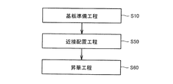
- a substrate preparation step is first performed as step (S10).
- step (S10) a plurality of SiC substrates are prepared as in the case of the first embodiment, and a raw material substrate made of silicon carbide is prepared.
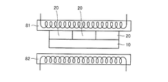
- the proximity placement step is performed as a step (S50).
- SiC substrate 20 and raw material substrate 11 are held by first heater 81 and second heater 82 arranged to face each other.
- SiC substrate 20 and raw material substrate 11 are arranged close to each other so that their main surfaces face each other at an interval of 1 ⁇ m to 1 cm, for example, an interval of about 1 mm.
- a sublimation process is implemented as process (S60).
- the SiC substrate 20 is heated to a predetermined substrate temperature by the first heater 81.
- the raw material substrate 11 is heated to a predetermined raw material temperature by the second heater 82.
- SiC is sublimated from the surface of the raw material substrate by heating the raw material substrate 11 to the raw material temperature.
- the substrate temperature is set lower than the raw material temperature. Specifically, for example, the substrate temperature is set to be lower by about 1 ° C. to 100 ° C. than the raw material temperature.
- the substrate temperature is, for example, not less than 1800 ° and not more than 2500 ° C.
- step (S60) is completed, and silicon carbide substrate 1 shown in FIG. 1 is completed.
- silicon carbide substrate 1 in the third embodiment basically has the same configuration as silicon carbide substrate 1 in the first embodiment, and exhibits the same effect.
- silicon carbide substrate 1 in the third embodiment is different from that of the first embodiment in that SiC bonding layer 40 as an intermediate layer is formed between base substrate 10 and SiC substrate 20. There is.
- SiC bonding layer 40 as an intermediate layer made of silicon carbide is arranged between base substrate 10 and SiC substrate 20.
- the base substrate 10 and the SiC substrate 20 are connected by the SiC bonding layer 40. Due to the presence of the SiC bonding layer 40, the silicon carbide substrate 1 in which the base substrate 10 and the SiC substrate 20 are stacked can be easily manufactured.
- a substrate preparation step is first carried out as step (S10) in the same manner as in the first embodiment, and base substrate 10 and a plurality of substrates are prepared.
- a SiC substrate 20 is prepared.
- a Si layer forming step is performed as a step (S11).
- a Si layer having a thickness of, for example, about 100 nm is formed on one main surface of base substrate 10 prepared in step (S10).
- the formation of this Si layer can be performed, for example, by sputtering.
- a lamination step is performed as a step (S30).
- the plurality of SiC substrates 20 prepared in step (S10) are arranged side by side in plan view on the Si layer formed in step (S11).
- a laminated substrate in which the SiC substrate 20 is laminated on the base substrate 10 with the Si layer interposed therebetween is obtained.
- step (S70) a heating step is performed as a step (S70).
- the laminated substrate produced in step (S30) is heated to about 1500 ° C., for example, in a mixed gas atmosphere of hydrogen gas and propane gas at a pressure of 1 ⁇ 10 3 Pa, for about 3 hours. It is held.
- carbon is mainly supplied to the above-mentioned Si layer by diffusion from the base substrate 10 and the SiC substrate 20, and a SiC bonding layer 40 is formed as shown in FIG.
- silicon carbide substrate 1 in the third embodiment in which base substrate 10 and SiC substrate 20 are connected by SiC bonding layer 40 can be easily manufactured.
- silicon carbide substrate 1 in the fourth embodiment basically has the same configuration as silicon carbide substrate 1 in the first embodiment, and exhibits the same effect.
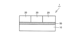
- silicon carbide substrate 1 in the fourth embodiment is different from that of the first embodiment in that ohmic contact layer 50 as an intermediate layer is formed between base substrate 10 and SiC substrate 20. There is.
- ohmic contact layer 50 as an intermediate layer formed by silicidation of at least a part of the metal layer is arranged between base substrate 10 and SiC substrate 20. It is done. The base substrate 10 and the SiC substrate 20 are connected by the ohmic contact layer 50. By the presence of ohmic contact layer 50, silicon carbide substrate 1 in which base substrate 10 and SiC substrate 20 are stacked can be easily manufactured.
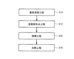
- a substrate preparation step is first carried out as step (S10) in the same manner as in the first embodiment, and base substrate 10 and a plurality of substrates are prepared.
- a SiC substrate 20 is prepared.
- a metal layer formation process is implemented as process (S12).
- a metal layer is formed, for example, by vapor-depositing a metal on one main surface of base substrate 10 prepared in step (S10).
- the metal layer contains at least one selected from metals which form silicides when heated, such as nickel, molybdenum, titanium, aluminum, and tungsten.
- a lamination step is performed as a step (S30).
- the plurality of SiC substrates 20 prepared in step (S10) are placed on the metal layer formed in step (S12).
- a laminated substrate in which the SiC substrate 20 is laminated on the base substrate 10 with the metal layer interposed therebetween is obtained.
- a heating step is performed as a step (S70).
- the laminated substrate produced in step (S30) is heated to about 1000 ° C. in an inert gas atmosphere such as argon.
- an inert gas atmosphere such as argon.
- the metal layer a region in contact with base substrate 10 and a region in contact with the SiC substrate
- ohmic contact layer 50 is formed.
- silicon carbide substrate 1 in the fifth embodiment in which base substrate 10 and SiC substrate 20 are connected by ohmic contact layer 50 can be easily manufactured.
- the intermediate layer is not limited thereto.
- carbon adhesive may be substituted for these.
- a SiC-based adhesive which is formed of an organic compound containing a silicon atom and a carbon atom in its structure to be silicon carbide by heat treatment.
- base substrate 10 and SiC substrate 20 may be bonded by thermocompression bonding.
- base substrate 10 in the said embodiment, what consists of various raw materials is employable.
- base substrate 10 when base substrate 10 is made of silicon carbide, base substrate 10 may be any of a sintered body, an amorphous, a polycrystal, and a single crystal.
- main surface 10A on the side facing SiC substrate 20 may be a ⁇ 0001 ⁇ plane or may have an off angle with respect to the ⁇ 0001 ⁇ plane. In this case, the off angle can be set arbitrarily, but for example, a value of 2 ° or less, more specifically, 1 ° or 2 ° can be adopted.
- the main surface 10A may be a surface on the Si surface side or a surface on the C surface side.
- the surface on the Si surface side refers to a surface having an angle of less than 90 ° with the Si surface, that is, the (0001) surface.
- the surface on the C surface side refers to a surface having an angle of less than 90 ° with the C surface, ie, the (000-1) surface.
- SiC substrate 20 in the above embodiment is made of single crystal silicon carbide.
- the main surface 20A opposite to the base substrate 10 may be a ⁇ 0001 ⁇ plane or may have an off angle with respect to the ⁇ 0001 ⁇ plane.
- the off angle can be set arbitrarily, but for example, a value such as 8 ° or less, more specifically 8 ° or 4 ° can be adopted, and an off angle of 4 ° or less such as 3 ° or 2 ° Corners may be employed.
- the main surface 20A may be a surface on the Si surface side or a surface on the C surface side.
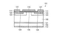
- a semiconductor device 101 is a vertical DiMOSFET (Double Implanted MOSFET), and includes a substrate 102, a buffer layer 121, a breakdown voltage holding layer 122, ap region 123, an n + region 124, and p + A region 125, an oxide film 126, a source electrode 111 and an upper source electrode 127, a gate electrode 110, and a drain electrode 112 formed on the back side of the substrate 102 are provided.
- a vertical DiMOSFET Double Implanted MOSFET
- buffer layer 121 made of silicon carbide is formed on the surface of substrate 102 made of silicon carbide of n type conductivity.
- substrate 102 the silicon carbide substrate of the present invention including silicon carbide substrate 1 described in the first to fourth embodiments is employed.
- buffer layer 121 is formed on SiC substrate 20 of silicon carbide substrate 1.
- Buffer layer 121 has n type conductivity and its thickness is, for example, 0.5 ⁇ m.
- concentration of the n-type conductive impurity in buffer layer 121 can be, for example, 5 ⁇ 10 17 cm ⁇ 3 .
- a breakdown voltage holding layer 122 is formed on the buffer layer 121.
- This withstand voltage holding layer 122 is made of silicon carbide of n type conductivity, and its thickness is, for example, 10 ⁇ m. Further, as the concentration of the n-type conductive impurity in breakdown voltage holding layer 122, a value such as 5 ⁇ 10 15 cm ⁇ 3 can be used, for example.
- p regions 123 of p type conductivity are formed spaced apart from each other. Inside p region 123, n + region 124 is formed in the surface layer of p region 123. In addition, a p + region 125 is formed at a position adjacent to the n + region 124. Over the n + region 124 in one p region 123, the breakdown voltage holding layer 122 exposed between the p region 123 and the two p regions 123, the other p region 123, and the n + region 124 in the other p region 123 The oxide film 126 is formed to extend to the top. Gate electrode 110 is formed on oxide film 126.
- the source electrode 111 is formed on the n + region 124 and the p + region 125.
- An upper source electrode 127 is formed on the source electrode 111.
- the drain electrode 112 is formed on the back surface which is the surface opposite to the surface on which the buffer layer 121 is formed.
- the silicon carbide substrate of the present invention such as silicon carbide substrate 1 described in the first to fourth embodiments above is employed as substrate 102. That is, semiconductor device 101 includes substrate 102 as a silicon carbide substrate, buffer layer 121 and withstand voltage holding layer 122 as epitaxial growth formed on substrate 102, and source electrode 111 formed on withstand voltage holding layer 122. Have.
- the substrate 102 is a silicon carbide substrate of the present invention, such as the silicon carbide substrate 1.
- the silicon carbide substrate of the present invention is a silicon carbide substrate that can realize the reduction of the manufacturing cost of the semiconductor device using the silicon carbide substrate. Therefore, the semiconductor device 101 is a semiconductor device whose manufacturing cost is reduced.
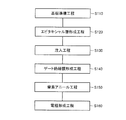
- a substrate preparation step (S110) is performed.
- a substrate 102 (see FIG. 13) having a main surface made of silicon carbide and having an off angle of about 8 ° with respect to the (0001) plane is prepared.
- the silicon carbide substrate of the present invention including the silicon carbide substrate 1 described in the first to fourth embodiments is prepared.
- the substrate 102 for example, a substrate having n type conductivity and a substrate resistance of 0.02 ⁇ cm may be used.
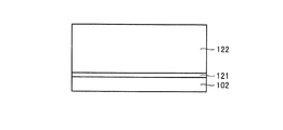
- buffer layer 121 is formed on the surface of substrate 102.
- Buffer layer 121 is formed on SiC substrate 20 of silicon carbide substrate 1 employed as substrate 102 (see FIGS. 1, 7 and 9).
- Buffer layer 121 is made of silicon carbide of n type conductivity, and forms an epitaxial growth layer having a thickness of 0.5 ⁇ m, for example.
- the concentration of the conductive impurity in buffer layer 121 can have a value of, for example, 5 ⁇ 10 17 cm ⁇ 3 .
- a withstand voltage holding layer 122 is formed on the buffer layer 121 as shown in FIG.
- a layer made of silicon carbide of n conductivity type is formed by epitaxial growth.
- a value such as 10 ⁇ m can be used as the thickness of pressure resistant holding layer 122.
- concentration of the n-type conductive impurity in breakdown voltage holding layer 122 for example, a value such as 5 ⁇ 10 15 cm ⁇ 3 can be used.
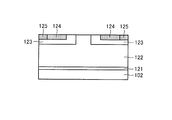
- the injection step (S130) is performed. More specifically, p-type region 123 is implanted as shown in FIG. 14 by implanting an impurity of p-type conductivity into breakdown voltage holding layer 122 using an oxide film formed by photolithography and etching as a mask. Form. Further, after removing the used oxide film, an oxide film having a new pattern is formed again using photolithography and etching. Then, an n + -type region 124 is formed by implanting an n-type conductive impurity into a predetermined region using the oxide film as a mask. Further, p + -type region 125 is formed by implanting a conductive impurity of p-type conductivity by a similar method. As a result, a structure as shown in FIG. 14 is obtained.
- activation annealing is performed.
- conditions such as a heating temperature of 1700 ° C. and a heating time of 30 minutes can be used using, for example, argon gas as an atmosphere gas.
- the gate insulating film forming step (S140) is performed. Specifically, as shown in FIG. 15, an oxide film 126 is formed to cover the withstand voltage holding layer 122, the p region 123, the n + region 124, and the p + region 125.
- a condition for forming this oxide film 126 for example, dry oxidation (thermal oxidation) may be performed.
- dry oxidation thermal oxidation
- conditions for this dry oxidation conditions such as a heating temperature of 1200 ° C. and a heating time of 30 minutes can be used.
- a nitrogen annealing step (S150) is performed. Specifically, the annealing process is performed with the atmosphere gas as nitrogen monoxide (NO). As temperature conditions of annealing treatment, for example, the heating temperature is set to 1100 ° C., and the heating time is set to 120 minutes. As a result, nitrogen atoms are introduced in the vicinity of the interface between the oxide film 126 and the lower breakdown voltage holding layer 122, the p region 123, the n + region 124, and the p + region 125.
- annealing may be performed using argon (Ar) gas which is an inert gas. Specifically, argon gas may be used as the atmosphere gas, and the heating temperature may be 1100 ° C., and the heating time may be 60 minutes.
- an electrode formation step (S160) is performed. Specifically, referring to FIG. 11, gate electrode 110, source electrode 111, drain electrode 112, and upper source electrode 127 are formed, and semiconductor device 101 is completed.
- the vertical MOSFET is described as an example of the semiconductor device that can be manufactured using the silicon carbide substrate of the present invention, but the semiconductor device that can be manufactured is not limited to this.
- various semiconductor devices such as JFET (Junction Field Effect Transistor), IGBT (Insulated Gate Bipolar Transistor), Schottky barrier diode, etc. can be manufactured using the silicon carbide substrate of the present invention. It is.
- a semiconductor device can be manufactured using the silicon carbide substrate of the present invention. That is, in the semiconductor device of the present invention, an epitaxial growth layer as an active layer is formed on the silicon carbide substrate of the present invention. More specifically, the semiconductor device of the present invention includes the silicon carbide substrate of the present invention, an epitaxial growth layer formed on the silicon carbide substrate, and an electrode formed on the epitaxial growth layer. That is, the semiconductor device of the present invention is formed on the base substrate, the SiC substrate made of single crystal silicon carbide and disposed on the base substrate, the epitaxial growth layer formed on the SiC substrate, and the epitaxial layer. And an electrode. The main surface of the SiC substrate opposite to the base substrate has an off angle of 20 ° or less with respect to the ⁇ 0001 ⁇ plane.
- the silicon carbide substrate of the present invention can be particularly advantageously applied to a silicon carbide substrate used for manufacturing a semiconductor device for which reduction in manufacturing cost is required.
- Reference Signs List 1 silicon carbide substrate, 10 base substrate, 10A main surface, 11 raw material substrate, 20 SiC substrate, 20A main surface, 40 SiC bonding layer, 50 ohmic contact layer, 81 first heater, 82 second heater, 101 semiconductor device, 102 Substrate, 110 gate electrode, 111 source electrode, 112 drain electrode, 121 buffer layer, 122 withstand voltage holding layer, 123 p region, 124 n + region, 125 p + region, 126 oxide film, 127 upper source electrode.
Landscapes
- Chemical & Material Sciences (AREA)
- Engineering & Computer Science (AREA)
- Crystallography & Structural Chemistry (AREA)
- Materials Engineering (AREA)
- Metallurgy (AREA)
- Organic Chemistry (AREA)
- Inorganic Chemistry (AREA)
- Recrystallisation Techniques (AREA)
- Crystals, And After-Treatments Of Crystals (AREA)
- Electrodes Of Semiconductors (AREA)
Abstract
Description
まず、本発明の一実施の形態である実施の形態1について説明する。図1を参照して、本実施の形態における炭化珪素基板1は、直径70mm以上の炭化珪素(たとえば単結晶炭化珪素)からなるベース基板10と、単結晶炭化珪素からなり、ベース基板10上に平面的に見て並べて配置された複数のSiC基板20とを備えている。そして、SiC基板20のベース基板10とは反対側の主面20Aは、{0001}面に対するオフ角が20°以下となっている。
次に、本発明の他の実施の形態である実施の形態2について説明する。図1を参照して、実施の形態2における炭化珪素基板1は、実施の形態1における炭化珪素基板1と基本的には同様の構造を有し、同様の効果を奏する。しかし、実施の形態2における炭化珪素基板1は、その製造方法において実施の形態1の場合とは異なっている。
次に、本発明のさらに他の実施の形態である実施の形態3について説明する。図7を参照して、実施の形態3における炭化珪素基板1は、基本的には実施の形態1における炭化珪素基板1と同様の構成を有し、同様の効果を奏する。しかし、実施の形態3における炭化珪素基板1は、ベース基板10とSiC基板20との間に中間層としてのSiC接合層40が形成されている点において、実施の形態1の場合とは異なっている。
次に、本発明のさらに他の実施の形態である実施の形態4について説明する。図9を参照して、実施の形態4における炭化珪素基板1は、基本的には実施の形態1における炭化珪素基板1と同様の構成を有し、同様の効果を奏する。しかし、実施の形態4における炭化珪素基板1は、ベース基板10とSiC基板20との間に中間層としてのオーミックコンタクト層50が形成されている点において、実施の形態1の場合とは異なっている。
次に、上記本発明の炭化珪素基板を用いて作製される半導体装置の一例を実施の形態5として説明する。図11を参照して、本発明による半導体装置101は、縦型DiMOSFET(Double Implanted MOSFET)であって、基板102、バッファ層121、耐圧保持層122、p領域123、n+領域124、p+領域125、酸化膜126、ソース電極111および上部ソース電極127、ゲート電極110および基板102の裏面側に形成されたドレイン電極112を備える。具体的には、導電型がn型の炭化珪素からなる基板102の表面上に、炭化珪素からなるバッファ層121が形成されている。基板102としては、上記実施の形態1~4において説明した炭化珪素基板1を含む本発明の炭化珪素基板が採用される。そして、上記実施の形態1~4の炭化珪素基板1が採用される場合、バッファ層121は、炭化珪素基板1のSiC基板20上に形成される。バッファ層121は導電型がn型であり、その厚みはたとえば0.5μmである。また、バッファ層121におけるn型の導電性不純物の濃度はたとえば5×1017cm-3とすることができる。このバッファ層121上には耐圧保持層122が形成されている。この耐圧保持層122は、導電型がn型の炭化珪素からなり、たとえばその厚みは10μmである。また、耐圧保持層122におけるn型の導電性不純物の濃度としては、たとえば5×1015cm-3といった値を用いることができる。
Claims (7)
- 直径70mm以上のベース基板(10)と、
単結晶炭化珪素からなり、前記ベース基板上に平面的に見て並べて配置された複数のSiC基板(20)とを備え、
前記SiC基板(20)の前記ベース基板(10)とは反対側の主面(20A)は、{0001}面に対するオフ角が20°以下となっている、炭化珪素基板(1)。 - 前記ベース基板(10)と前記SiC基板(20)とは互いに接触している、請求項1に記載の炭化珪素基板(1)。
- 前記ベース基板(10)は炭化珪素からなっている、請求項1に記載の炭化珪素基板(1)。
- 前記ベース基板(10)と前記SiC基板(20)との間において、結晶が不連続となっている、請求項3に記載の炭化珪素基板(1)。
- 前記ベース基板(10)と前記SiC基板(20)との間において、欠陥が不連続となっている、請求項4に記載の炭化珪素基板(1)。
- 前記ベース基板(10)の直径は4インチ以上である、請求項1に記載の炭化珪素基板(1)。
- 前記SiC基板(20)の前記ベース基板(10)とは反対側の主面は、{0001}面に対するオフ角が5°以上となっている、請求項1に記載の炭化珪素基板(1)。
Priority Applications (3)
| Application Number | Priority Date | Filing Date | Title |
|---|---|---|---|
| CN2011800213549A CN102869816A (zh) | 2011-03-22 | 2011-12-19 | 碳化硅衬底 |
| JP2012536628A JPWO2012127748A1 (ja) | 2011-03-22 | 2011-12-19 | 炭化珪素基板 |
| DE112011105073T DE112011105073T5 (de) | 2011-03-22 | 2011-12-19 | Siliziumkarbidsubstrat |
Applications Claiming Priority (2)
| Application Number | Priority Date | Filing Date | Title |
|---|---|---|---|
| JP2011-062123 | 2011-03-22 | ||
| JP2011062123 | 2011-03-22 |
Publications (1)
| Publication Number | Publication Date |
|---|---|
| WO2012127748A1 true WO2012127748A1 (ja) | 2012-09-27 |
Family
ID=46877569
Family Applications (1)
| Application Number | Title | Priority Date | Filing Date |
|---|---|---|---|
| PCT/JP2011/079348 Ceased WO2012127748A1 (ja) | 2011-03-22 | 2011-12-19 | 炭化珪素基板 |
Country Status (6)
| Country | Link |
|---|---|
| US (1) | US20120244307A1 (ja) |
| JP (1) | JPWO2012127748A1 (ja) |
| CN (1) | CN102869816A (ja) |
| DE (1) | DE112011105073T5 (ja) |
| TW (1) | TW201239142A (ja) |
| WO (1) | WO2012127748A1 (ja) |
Cited By (1)
| Publication number | Priority date | Publication date | Assignee | Title |
|---|---|---|---|---|
| JP2014154885A (ja) * | 2013-02-12 | 2014-08-25 | Infineon Technologies Ag | 複合材ウェハおよびその製造方法 |
Families Citing this family (4)
| Publication number | Priority date | Publication date | Assignee | Title |
|---|---|---|---|---|
| JP5814881B2 (ja) * | 2012-07-31 | 2015-11-17 | 株式会社東芝 | トランジスタ及びその製造方法 |
| JP6331634B2 (ja) * | 2014-04-17 | 2018-05-30 | 住友電気工業株式会社 | 炭化珪素半導体装置の製造方法 |
| DE112015006024B9 (de) * | 2015-01-21 | 2025-04-24 | Sumitomo Electric Industries, Ltd. | Verfahren zum Herstellen eines Siliziumkarbid-Einkristalls, Siliziumkarbid-Einkristallsubstrat und Siliziumkarbid-Epitaxiesubstrat |
| JP6816710B2 (ja) * | 2015-10-13 | 2021-01-20 | 住友電気工業株式会社 | 半導体積層体 |
Citations (4)
| Publication number | Priority date | Publication date | Assignee | Title |
|---|---|---|---|---|
| JPH1187200A (ja) * | 1997-09-05 | 1999-03-30 | Toshiba Corp | 半導体基板及び半導体装置の製造方法 |
| JP2003527298A (ja) * | 2000-03-13 | 2003-09-16 | トゥー‐シックス・インコーポレイテッド | タイル張りされた種結晶の相互成長による大型単結晶種結晶の作製 |
| WO2010087518A1 (ja) * | 2009-01-30 | 2010-08-05 | 新日本製鐵株式会社 | エピタキシャル炭化珪素単結晶基板及びその製造方法 |
| WO2010131568A1 (ja) * | 2009-05-11 | 2010-11-18 | 住友電気工業株式会社 | 炭化珪素基板、半導体装置および炭化珪素基板の製造方法 |
Family Cites Families (6)
| Publication number | Priority date | Publication date | Assignee | Title |
|---|---|---|---|---|
| JPS63260014A (ja) * | 1986-12-09 | 1988-10-27 | Sharp Corp | 炭化珪素単結晶薄膜の形成方法 |
| JPS63277596A (ja) * | 1987-05-07 | 1988-11-15 | Sharp Corp | 炭化珪素単結晶の成長方法 |
| JPH0322526A (ja) * | 1989-06-20 | 1991-01-30 | Sharp Corp | 炭化珪素半導体装置の製造方法 |
| US6270573B1 (en) * | 1997-08-27 | 2001-08-07 | Matsushita Electric Industrial Co., Ltd. | Silicon carbide substrate, and method for producing the substrate, and semiconductor device utilizing the substrate |
| DE60020737T2 (de) * | 1999-09-06 | 2006-03-16 | Sixon Inc. | Sic-einkristall und herstellungsverfahren dafür |
| JP2009081352A (ja) * | 2007-09-27 | 2009-04-16 | Seiko Epson Corp | 半導体基板の製造方法及び半導体基板 |
-
2011
- 2011-12-19 JP JP2012536628A patent/JPWO2012127748A1/ja active Pending
- 2011-12-19 WO PCT/JP2011/079348 patent/WO2012127748A1/ja not_active Ceased
- 2011-12-19 CN CN2011800213549A patent/CN102869816A/zh active Pending
- 2011-12-19 DE DE112011105073T patent/DE112011105073T5/de not_active Ceased
-
2012
- 2012-01-04 TW TW101100352A patent/TW201239142A/zh unknown
- 2012-03-21 US US13/425,889 patent/US20120244307A1/en not_active Abandoned
Patent Citations (4)
| Publication number | Priority date | Publication date | Assignee | Title |
|---|---|---|---|---|
| JPH1187200A (ja) * | 1997-09-05 | 1999-03-30 | Toshiba Corp | 半導体基板及び半導体装置の製造方法 |
| JP2003527298A (ja) * | 2000-03-13 | 2003-09-16 | トゥー‐シックス・インコーポレイテッド | タイル張りされた種結晶の相互成長による大型単結晶種結晶の作製 |
| WO2010087518A1 (ja) * | 2009-01-30 | 2010-08-05 | 新日本製鐵株式会社 | エピタキシャル炭化珪素単結晶基板及びその製造方法 |
| WO2010131568A1 (ja) * | 2009-05-11 | 2010-11-18 | 住友電気工業株式会社 | 炭化珪素基板、半導体装置および炭化珪素基板の製造方法 |
Cited By (1)
| Publication number | Priority date | Publication date | Assignee | Title |
|---|---|---|---|---|
| JP2014154885A (ja) * | 2013-02-12 | 2014-08-25 | Infineon Technologies Ag | 複合材ウェハおよびその製造方法 |
Also Published As
| Publication number | Publication date |
|---|---|
| US20120244307A1 (en) | 2012-09-27 |
| JPWO2012127748A1 (ja) | 2014-07-24 |
| TW201239142A (en) | 2012-10-01 |
| CN102869816A (zh) | 2013-01-09 |
| DE112011105073T5 (de) | 2013-12-24 |
Similar Documents
| Publication | Publication Date | Title |
|---|---|---|
| JP5344037B2 (ja) | 炭化珪素基板および半導体装置 | |
| WO2011046021A1 (ja) | 炭化珪素基板の製造方法および炭化珪素基板 | |
| JP2011243770A (ja) | 炭化珪素基板、半導体装置、炭化珪素基板の製造方法 | |
| WO2011142158A1 (ja) | 炭化珪素基板の製造方法、半導体装置の製造方法、炭化珪素基板および半導体装置 | |
| TW201201279A (en) | Silicon carbide substrate manufacturing method and manufacturing device | |
| JPWO2011052320A1 (ja) | 炭化珪素基板の製造方法および炭化珪素基板 | |
| JPWO2010131571A1 (ja) | 半導体装置 | |
| WO2012127748A1 (ja) | 炭化珪素基板 | |
| JPWO2011077797A1 (ja) | 炭化珪素基板 | |
| JPWO2011092893A1 (ja) | 炭化珪素基板の製造方法 | |
| JP2011243618A (ja) | 炭化珪素基板の製造方法、半導体装置の製造方法、炭化珪素基板および半導体装置 | |
| JP2011256053A (ja) | 複合基板およびその製造方法 | |
| WO2011152089A1 (ja) | 炭化珪素基板の製造方法、半導体装置の製造方法、炭化珪素基板および半導体装置 | |
| JP2011243617A (ja) | 炭化珪素基板の製造方法、半導体装置の製造方法、炭化珪素基板および半導体装置 | |
| JP2011243771A (ja) | 炭化珪素基板の製造方法、半導体装置の製造方法、炭化珪素基板および半導体装置 | |
| WO2011086734A1 (ja) | 炭化珪素基板の製造方法 | |
| JP2011243640A (ja) | 炭化珪素基板の製造方法、半導体装置の製造方法、炭化珪素基板および半導体装置 | |
| JP2011086660A (ja) | 炭化珪素基板の製造方法および炭化珪素基板 |
Legal Events
| Date | Code | Title | Description |
|---|---|---|---|
| WWE | Wipo information: entry into national phase |
Ref document number: 201180021354.9 Country of ref document: CN |
|
| ENP | Entry into the national phase |
Ref document number: 2012536628 Country of ref document: JP Kind code of ref document: A |
|
| 121 | Ep: the epo has been informed by wipo that ep was designated in this application |
Ref document number: 11861409 Country of ref document: EP Kind code of ref document: A1 |
|
| WWE | Wipo information: entry into national phase |
Ref document number: 1120111050739 Country of ref document: DE Ref document number: 112011105073 Country of ref document: DE |
|
| 122 | Ep: pct application non-entry in european phase |
Ref document number: 11861409 Country of ref document: EP Kind code of ref document: A1 |