WO2012124677A1 - High-voltage integrated circuit device - Google Patents
High-voltage integrated circuit device Download PDFInfo
- Publication number
- WO2012124677A1 WO2012124677A1 PCT/JP2012/056373 JP2012056373W WO2012124677A1 WO 2012124677 A1 WO2012124677 A1 WO 2012124677A1 JP 2012056373 W JP2012056373 W JP 2012056373W WO 2012124677 A1 WO2012124677 A1 WO 2012124677A1
- Authority
- WO
- WIPO (PCT)
- Prior art keywords
- region
- contact
- conductivity type
- mosfet
- disposed
- Prior art date
Links
Images


Classifications
-
- H—ELECTRICITY
- H01—ELECTRIC ELEMENTS
- H01L—SEMICONDUCTOR DEVICES NOT COVERED BY CLASS H10
- H01L21/00—Processes or apparatus adapted for the manufacture or treatment of semiconductor or solid state devices or of parts thereof
- H01L21/70—Manufacture or treatment of devices consisting of a plurality of solid state components formed in or on a common substrate or of parts thereof; Manufacture of integrated circuit devices or of parts thereof
- H01L21/71—Manufacture of specific parts of devices defined in group H01L21/70
- H01L21/76—Making of isolation regions between components
- H01L21/761—PN junctions
-
- G—PHYSICS
- G05—CONTROLLING; REGULATING
- G05F—SYSTEMS FOR REGULATING ELECTRIC OR MAGNETIC VARIABLES
- G05F3/00—Non-retroactive systems for regulating electric variables by using an uncontrolled element, or an uncontrolled combination of elements, such element or such combination having self-regulating properties
- G05F3/02—Regulating voltage or current
-
- H—ELECTRICITY
- H01—ELECTRIC ELEMENTS
- H01L—SEMICONDUCTOR DEVICES NOT COVERED BY CLASS H10
- H01L27/00—Devices consisting of a plurality of semiconductor or other solid-state components formed in or on a common substrate
- H01L27/02—Devices consisting of a plurality of semiconductor or other solid-state components formed in or on a common substrate including semiconductor components specially adapted for rectifying, oscillating, amplifying or switching and having at least one potential-jump barrier or surface barrier; including integrated passive circuit elements with at least one potential-jump barrier or surface barrier
- H01L27/04—Devices consisting of a plurality of semiconductor or other solid-state components formed in or on a common substrate including semiconductor components specially adapted for rectifying, oscillating, amplifying or switching and having at least one potential-jump barrier or surface barrier; including integrated passive circuit elements with at least one potential-jump barrier or surface barrier the substrate being a semiconductor body
- H01L27/08—Devices consisting of a plurality of semiconductor or other solid-state components formed in or on a common substrate including semiconductor components specially adapted for rectifying, oscillating, amplifying or switching and having at least one potential-jump barrier or surface barrier; including integrated passive circuit elements with at least one potential-jump barrier or surface barrier the substrate being a semiconductor body including only semiconductor components of a single kind
- H01L27/085—Devices consisting of a plurality of semiconductor or other solid-state components formed in or on a common substrate including semiconductor components specially adapted for rectifying, oscillating, amplifying or switching and having at least one potential-jump barrier or surface barrier; including integrated passive circuit elements with at least one potential-jump barrier or surface barrier the substrate being a semiconductor body including only semiconductor components of a single kind including field-effect components only
- H01L27/088—Devices consisting of a plurality of semiconductor or other solid-state components formed in or on a common substrate including semiconductor components specially adapted for rectifying, oscillating, amplifying or switching and having at least one potential-jump barrier or surface barrier; including integrated passive circuit elements with at least one potential-jump barrier or surface barrier the substrate being a semiconductor body including only semiconductor components of a single kind including field-effect components only the components being field-effect transistors with insulated gate
- H01L27/092—Devices consisting of a plurality of semiconductor or other solid-state components formed in or on a common substrate including semiconductor components specially adapted for rectifying, oscillating, amplifying or switching and having at least one potential-jump barrier or surface barrier; including integrated passive circuit elements with at least one potential-jump barrier or surface barrier the substrate being a semiconductor body including only semiconductor components of a single kind including field-effect components only the components being field-effect transistors with insulated gate complementary MIS field-effect transistors
- H01L27/0921—Means for preventing a bipolar, e.g. thyristor, action between the different transistor regions, e.g. Latchup prevention
-
- H—ELECTRICITY
- H01—ELECTRIC ELEMENTS
- H01L—SEMICONDUCTOR DEVICES NOT COVERED BY CLASS H10
- H01L27/00—Devices consisting of a plurality of semiconductor or other solid-state components formed in or on a common substrate
- H01L27/02—Devices consisting of a plurality of semiconductor or other solid-state components formed in or on a common substrate including semiconductor components specially adapted for rectifying, oscillating, amplifying or switching and having at least one potential-jump barrier or surface barrier; including integrated passive circuit elements with at least one potential-jump barrier or surface barrier
- H01L27/04—Devices consisting of a plurality of semiconductor or other solid-state components formed in or on a common substrate including semiconductor components specially adapted for rectifying, oscillating, amplifying or switching and having at least one potential-jump barrier or surface barrier; including integrated passive circuit elements with at least one potential-jump barrier or surface barrier the substrate being a semiconductor body
- H01L27/08—Devices consisting of a plurality of semiconductor or other solid-state components formed in or on a common substrate including semiconductor components specially adapted for rectifying, oscillating, amplifying or switching and having at least one potential-jump barrier or surface barrier; including integrated passive circuit elements with at least one potential-jump barrier or surface barrier the substrate being a semiconductor body including only semiconductor components of a single kind
- H01L27/085—Devices consisting of a plurality of semiconductor or other solid-state components formed in or on a common substrate including semiconductor components specially adapted for rectifying, oscillating, amplifying or switching and having at least one potential-jump barrier or surface barrier; including integrated passive circuit elements with at least one potential-jump barrier or surface barrier the substrate being a semiconductor body including only semiconductor components of a single kind including field-effect components only
- H01L27/088—Devices consisting of a plurality of semiconductor or other solid-state components formed in or on a common substrate including semiconductor components specially adapted for rectifying, oscillating, amplifying or switching and having at least one potential-jump barrier or surface barrier; including integrated passive circuit elements with at least one potential-jump barrier or surface barrier the substrate being a semiconductor body including only semiconductor components of a single kind including field-effect components only the components being field-effect transistors with insulated gate
- H01L27/092—Devices consisting of a plurality of semiconductor or other solid-state components formed in or on a common substrate including semiconductor components specially adapted for rectifying, oscillating, amplifying or switching and having at least one potential-jump barrier or surface barrier; including integrated passive circuit elements with at least one potential-jump barrier or surface barrier the substrate being a semiconductor body including only semiconductor components of a single kind including field-effect components only the components being field-effect transistors with insulated gate complementary MIS field-effect transistors
- H01L27/0922—Combination of complementary transistors having a different structure, e.g. stacked CMOS, high-voltage and low-voltage CMOS
Definitions
- the present invention relates to a high voltage integrated circuit device.
- High voltage integrated circuit devices are well known as means for driving on / off the switching power device that constitutes the upper arm of a bridge circuit for reverse power conversion (DC / AC conversion) such as a PWM inverter.
- a bridge circuit for reverse power conversion such as a PWM inverter.
- High-voltage junctions that do not perform potential insulation with transformers and photocouplers are used. Utilized element isolation HVIC is employed.
- FIG. 9 is an explanatory diagram showing a connection example of a switching power device that constitutes a power conversion device such as an inverter and a conventional HVIC that drives the switching power device.
- FIG. 9 shows an example of a half bridge in which two switching power devices (in this case, IGBTs 114 and 115: insulated gate bipolar transistors) are connected in series.
- the power converter shown in FIG. 9 alternately outputs a high potential or a low potential from the Vs terminal, which is the output terminal, by alternately turning on the IGBT 115 of the upper arm and the IGBT 114 of the lower arm of this half bridge, and the L load AC power is supplied to 118.
- the IGBT 114 and the IGBT 115 are operated so that the IGBT 115 of the upper arm is turned on and the IGBT 114 of the lower arm is turned off.
- the IGBT 114 and the IGBT 115 are operated such that the upper arm IGBT 115 is turned off and the lower arm IGBT 114 is turned on.
- the diodes connected in reverse parallel to the IGBTs 114 and 115 are free-wheeling diode FWDs (Free Wheel Diodes) 116 and 117, respectively.
- the gate signal to the IGBT 114 of the lower arm is output from L-OUT with reference to GND, and the gate signal to the IGBT 115 of the upper arm is based on the potential of the Vs terminal. Output from H-OUT.
- the HVIC 111 In order to output a signal from H-OUT on the basis of electricity at the Vs terminal, the HVIC 111 needs to have a level shift function.
- Vss in FIG. 9 indicates the high potential side of the high voltage power supply (main circuit power supply).
- GND is a ground (ground).
- Vs is an intermediate potential that varies from the Vss potential to the GND potential.
- H-VDD is a high potential side of the low voltage power supply 113 with the potential of the Vs terminal as a reference.
- L-VDD is the high potential side of the low voltage power supply 112 with respect to GND.
- H-IN is an input signal and an input terminal input to the gate of the low-side C-MOS circuit connected to the level-up circuit.
- L-IN is an input signal and an input terminal input to the gate of the low-side C-MOS circuit connected to the gate of the IGBT 114 of the lower arm.
- H-OUT is the output signal and output terminal of the high-side C-MOS circuit that outputs to the gate of the IGBT 115 of the upper arm.
- L-OUT is an output signal output to the gate of the lower arm IGBT 114 and an output terminal.
- ALM-IN is an input signal and an input terminal for the detection signal 119 when the temperature or overcurrent of the IGBT 115 of the upper arm is detected.
- ALM-OUT is an output signal and an output terminal of the detection signal leveled down.
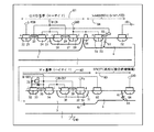
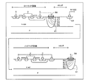
- FIG. 10 and 11 are circuit diagrams showing the level shift circuit and its peripheral circuits.
- FIG. 10 is a circuit diagram including a level-up circuit
- FIG. 11 is a circuit diagram including a level-down circuit.
- reference numeral 120 denotes a terminal on the high potential side of the low voltage power supply 113 with the Vs terminal as a reference.
- it means that electrons or holes are majority carriers in the layers and regions with n or p, respectively.
- + and ⁇ attached to n and p mean that the impurity concentration is higher and lower than that of the layer or region not attached thereto.
- peripheral circuits low-side (low-side circuit portion) C-MOS circuits (PMOS and NMOS) that transmit an input signal of the level shift circuit, and output signals (level-up circuit or level-down circuit) of the level shift circuit (level-up circuit or level-down circuit)
- a high-side (high-side circuit unit) C-MOS circuit (PMOS and NMOS) that transmits an output signal from the output unit 101 to the IGBT 115 of the upper arm is shown.
- Reference numeral 71 in FIG. 10 is a level shift resistor.
- Reference numeral 75 denotes a diode that boosts a boost trap capacitor (not shown), and is a boost trap diode that is boosted by a booster wrap voltage (corresponding to the voltage of the low voltage power supply 113) from the Vs voltage.
- the voltage of the low voltage power supply 113 and the voltage of the low voltage power supply 112 are the same.
- the level down circuit includes a p-channel MOSFET 43 and a level shift resistor 72.
- a diode 76 is connected to the level shift resistor 72 in parallel.
- the ALM-IN signal is input to the gate of the C-MOS circuit of the high side circuit section, and the output signal of the C-MOS circuit is input to the gate of the p-channel MOSFET 43 of the level down circuit.
- the p-channel MOSFET 43 is turned on / off.
- a signal from the output unit 102 of the level down circuit to the low side (low side circuit unit) is output.
- an ALM-OUT signal level-down from the output of the CMOS circuit in the low side circuit section is output from the low side circuit section as a detection signal.
- the HVIC 111 shown in FIG. 9 has terminals (H-VDD, H-OUT, ALM-IN, L-VDD, L-OUT, GND, H-IN, ALM-OUT, L-) for inputting / outputting the above signals. IN). These correspond to the terminals in FIGS. 10 and 11.
- the bridge circuit manufactured by combining the half-bridge circuit composed of the switching power devices (IGBTs 114 and 115) shown in FIG. 9 is an inverter for motor control, a large capacity PDP (plasma display panel), and a liquid crystal panel. It is widely used in many fields such as power supply applications such as inverters for home appliances such as air conditioners and lighting.
- FIG. 12 is a circuit diagram showing in detail a level shift circuit of a conventional high voltage integrated circuit device. 12A is a level-up circuit diagram, and FIG. 12B is a level-down circuit diagram.
- the level-up circuit shown in FIG. 12A includes a level shift resistor 71 and an n-channel MOSFET 41 to which the level shift resistor 71 and the drain are connected, and the connection between the level shift resistor 71 and the n-channel MOSFET 41 is leveled up.
- the circuit is configured as an output unit 101.
- the diode 75 is connected in parallel.
- the diode 75 when an overvoltage is applied to the H-VDD terminal, the diode 75 has a function of preventing an excessive voltage from being applied to the gate of the MOSFET of the C-MOS circuit in the high side circuit section. In general, a Zener diode is frequently used as the diode 75.
- the n-channel MOSFET 41 includes a body diode 42 connected in antiparallel.
- the level down circuit shown in FIG. 12B includes a drain of the p-channel MOSFET 43 and a level shift resistor 72 connected to the drain, and the connection between the level shift resistor 72 and the p-channel MOSFET 43 is a level down circuit.
- the output unit 102 is configured.
- a diode 76 is connected to the level shift resistor 72 in parallel.
- the diode 76 when an overvoltage is applied to the H-VDD terminal when the MOSFET 43 is on, the diode 76 has a function of preventing an overvoltage from being applied to the gate of the MOSFET of the C-MOS circuit in the low side circuit section.
- the n-channel MOSFET 43 includes a body diode 44 connected in antiparallel.
- FIG. 13 is a cross-sectional view showing the main parts of the logic part of the high-side circuit part, the logic part of the low-side circuit part, and the level-up circuit part of the self-isolation type high voltage integrated circuit device.
- n ⁇ region 2 and n region 3 which are n well regions are formed in the surface layer of p type semiconductor substrate 1 connected to the GND potential.
- n ⁇ region 2 for example, a C-MOS circuit or the like constituting the logic part of the low side circuit part 91 is formed.
- n region 3 for example, a C-MOS circuit or the like constituting the logic unit of the level shift circuit unit 94 or the high side circuit unit 92 is formed.
- the level-shifting (here, level-up) n-channel MOSFET 41 is in contact with the n ⁇ region 4, a p region 51 serving as a base region, an n + region 53 that is a source formed in the p region 51, and a p contact region 54.
- the gate electrode 55 is formed on the n + region 52, which is the drain formed in the n ⁇ region 4, and on the p region 51 sandwiched between the n + region 53 and the n + region 52 through a gate oxide film. Composed.
- reference numerals 22 and 32 are n + regions
- reference numerals 28 and 38 are p + regions.
- Reference numeral 56 denotes a p + region as a first contact region
- reference numeral 62 denotes an n + region as a second contact region
- reference numeral 93 denotes a high breakdown voltage junction termination region.
- Reference numerals 45 and 46 are parasitic pn diodes
- reference numerals a to j are electrodes.
- the n + region 52 which is the drain of the n-channel MOSFET 41 is connected to the H-VDD terminal via the level shift resistor 71 by the surface metal wiring. Further, the connection portion between the n + region 52 that is the drain and the level shift resistor 71 becomes the output portion 101 of the level-up circuit. Since the output unit 101 outputs a low potential when the level shift n-channel MOSFET 41 is turned on and outputs a high potential when the level shift n-channel MOSFET 41 is turned off, the output unit 101 can perform a level shift operation that is signal transmission between different reference potentials.
- V S0 L0 ⁇ dI / dt (1)
- V spy is the battery voltage across the high-side low voltage power supply 113 or bootstrap capacitor (not shown)
- V fd is the forward voltage drop across the parasitic pn diodes 45 and 46.
- the negative surge voltage V S0 applied is the product of the parasitic inductance component (L1) due to the wiring on the printed circuit board, the cable up to the L load 118, etc., and dI1 / dt according to the off-period of the on-current I1 flowing in the IGBT 115.
- This spike-like negative surge voltage V S0 is applied to the Vs terminal in proportion to (L1 ⁇ (dI1 / dt)).
- the applied voltage is about ⁇ 100 V, and the applied period is about several hundred ns to 1 ⁇ s.
- a circuit for protecting a high voltage integrated circuit for driving a half-bridge power transistor is disclosed.
- the circuit is intended for circuits that anticipate excessive negative swings at the output node and is a high voltage integrated circuit chip with a resistor between the substrate and ground that limits the current during the negative voltage spike (eg, (See Patent Document 1 below.)
- the drain of the switching element belonging to the level shifter, the level shift resistor, and the current limiting resistor are connected in series, and the level shift resistor and the current limiting resistor are connected to the output unit of the level up circuit.
- the level shift resistor and the current limiting resistor are connected to the output unit of the level up circuit.
- a p + -type impurity region is formed adjacent to the p-well for forming the n-channel MOSFET in the C-MOS logic in the high-side circuit portion formed of the n-well formed on the p-substrate and connected to the Vs potential. .
- an n + type impurity region and a p + type impurity region connected to the H-VDD potential are provided on the n well.
- the conventional high voltage integrated circuit device described above has the following problems.
- the Vss voltage is about 1200 V and the H-VDD potential is about 20 V higher than the Vs potential
- the IGBT 115 of the upper arm operates and the lower arm
- a current flows from the upper arm IGBT 115 to the L load 118.
- the p semiconductor substrate 1 and the p region 61 are at the GND potential. Therefore, when the potential of the Vs terminal is lowered until both the n region 3 which is the n well region and the n ⁇ region 4 which is the n ⁇ well region are lower than the GND potential, the parasitic pn composed of the p semiconductor substrate 1 and the n region 3
- the diode 45 and the parasitic pn diode 46 composed of the p region 61 and the n ⁇ region 4 are forward biased, and a large current flows.
- Patent Document 1 a resistor for limiting current is connected between the ground (ground) terminal and the substrate, and the connection at other locations is not mentioned. Since this resistor is formed of a polysilicon layer, when a large pulse current (several A to several tens of A) due to a negative surge voltage flows transiently to a parasitic diode between the Vs terminal and the ground terminal, the polysilicon is There is a possibility that the layer is melted by overcurrent and the HVIC is destroyed.
- Patent Document 2 a diode is connected to reduce the effect of reverse bias, and a resistor that limits the current of the body diode and the parasitic diode when the H-VDD potential becomes negative due to the L load. There is no mention of the layout method.
- Patent Document 3 a current limiting resistor is connected to a path between a high potential side (H-VDD) and a low potential side (ground) of a Vs reference low voltage power source of a level shift circuit, whereby n It has been proposed that the body diode of the channel MOSFET and the parasitic diode itself are destroyed by overcurrent, and that the portion having a small current capacity of the level shift circuit is prevented from being overcurrent destroyed. However, there is no mention of preventing parasitic malfunction (false inversion) of the Vs-based high-side logic (C-MOS circuit) and the ground-based low-side logic (C-MOS circuit).
- n + -type and p + -type impurity regions are fixed to the H-VDD potential and the VS potential in the high-side well region in order to prevent parasitic malfunction of the Vs-based high-side logic due to the negative surge voltage. It is clearly stated that However, there is no mention of preventing malfunction of the logic part of the low side circuit part.
- FIG. 14 is an explanatory diagram showing a malfunction of the low side circuit portion and the high side circuit portion of the conventional high voltage integrated circuit device.
- the cross-sectional configuration of the HVIC shown in FIG. 14 corresponds to the cross-sectional configuration of the HVIC shown in FIG. 13, and is a cross-sectional configuration of the low side circuit portion 91, the high breakdown voltage junction termination region (HVJT) 93 and the high side circuit portion 92.
- HVJT high breakdown voltage junction termination region
- FIG. 14 the level-up circuit shown in FIG. 13 is not shown.
- the potential of n ⁇ region 2 below 24 is pulled down by a voltage drop.
- the low-side circuit unit 91 also has a parasitic pnp bipolar transistor 79 having the p + region 24 which is the drain of the p-channel MOSFET constituting the logic unit as an emitter, the n ⁇ region 2 as a base, and the p semiconductor substrate 1 as a collector. Turns on. For this reason, there is a possibility that malfunction such as inversion of the output logic of the L-OUT terminal or destruction due to latch-up of the low side circuit unit 91 may occur.
- the holes of minority carriers that have entered the n ⁇ region 4 flow into the p + regions 33 and 34 that are the source and drain of the p-channel MOSFET that constitutes the logic portion of the high side circuit portion 92, or the p offset region.
- the parasitic npn transistor composed of the n + region 37 that is the source of the n-channel MOSFET, the p region 31 that is the p offset region, and the n region 3 is turned on, and the logic portion of the high side circuit portion 92 malfunctions. And there is a risk of destruction due to latch-up.
- Reference numerals 25, 29, 35, and 39 in FIG. 14 are gate electrodes.
- the present invention is a low-side circuit (connected to the ground reference and internal power supply, L-VDD power supply when a negative voltage is applied to the H-VDD terminal or the Vs terminal). It is an object of the present invention to provide a high voltage integrated circuit device capable of preventing malfunction and destruction of a part.
- a high voltage integrated circuit device has the following characteristics.
- a second conductivity type low-side circuit portion connected to a low-voltage power source based on the GND potential is disposed.
- a second conductivity type high-side circuit portion connected to a low-voltage power supply with an intermediate potential higher than the GND potential as a reference is disposed on the semiconductor substrate, apart from the low-side circuit portion.
- a first conductivity type region that is electrically connected to the GND potential is disposed so as to surround the high side circuit portion, and forms a high breakdown voltage junction termination region together with an outer peripheral portion of the low side circuit portion.
- a first pickup electrode is disposed in the first conductivity type region.
- a second pickup electrode connected to the high potential side of the low voltage power source with the intermediate potential as a reference is disposed inside the high breakdown voltage junction termination region and on the outer periphery of the high side circuit portion.
- a first conductivity type first high-concentration contact region that is in ohmic contact with the first pickup electrode is provided.
- a second conductivity type second high-concentration contact region that is in ohmic contact with the second pickup electrode is provided.
- At least one of the first high-concentration contact region and the second high-concentration contact region is a universal contact region having a configuration in which p regions and n regions are alternately arranged along the surface of the semiconductor substrate. It is set as the structure which is.
- a high voltage integrated circuit device has the following characteristics.
- a second conductivity type first semiconductor region having a low-side circuit portion disposed on the first conductivity type semiconductor substrate is provided.
- a second conductive type second semiconductor region having a high side circuit portion disposed apart from the first semiconductor region is provided on the semiconductor substrate.
- a second MOSFET having a second conductivity type source region and a second conductivity type drain region disposed in a surface layer of the third semiconductor region.
- a MOS circuit is provided.
- a third MOSFET having a first conductivity type source region and a first conductivity type drain region disposed on a surface layer of the second semiconductor region; and a third MOSFET disposed on a surface layer of the second semiconductor region apart from the third MOSFET.
- a second MOSFET having a first conductivity type fourth semiconductor region and a fourth MOSFET having a second conductivity type source region and a second conductivity type drain region disposed in a surface layer of the fourth semiconductor region.
- a MOS circuit is provided.
- a fifth semiconductor region of a first conductivity type having a higher impurity concentration than that of the semiconductor substrate is provided on the surface layer of the semiconductor substrate and surrounds the second semiconductor region.
- a first conductivity type first contact region having a higher impurity concentration than the fifth semiconductor region is disposed on a surface layer of the fifth semiconductor region.
- the fifth semiconductor region and the outer periphery of the second semiconductor region constitute a high breakdown voltage junction termination region.
- a second contact region of a second conductivity type having a higher impurity concentration than the second semiconductor region is disposed on the surface layer of the second semiconductor region and inside the high breakdown voltage junction termination region.
- a third contact region of a second conductivity type that is in contact with the source region of the first MOSFET is disposed on the surface layer of the first semiconductor region.
- a fourth contact region of the first conductivity type that is in contact with the source region of the second MOSFET is disposed on the surface layer of the third semiconductor region.
- a fifth contact region of the second conductivity type that is in contact with the source region of the third MOSFET is disposed on the surface layer of the second semiconductor region.
- a sixth contact region of the first conductivity type that is in contact with the source region of the fourth MOSFET is disposed on the surface layer of the fourth semiconductor region.
- a first pickup electrode that is in ohmic contact with the first contact region is disposed on the first contact region.
- a second pickup electrode that is in ohmic contact with the second contact region is disposed on the second contact region.
- a first source electrode in contact with the source region and the third contact region of the first MOSFET is provided.
- a first drain electrode in contact with the drain region of the first MOSFET is provided.
- a second source electrode in contact with the source region and the fourth contact region of the second MOSFET is provided.
- a second drain electrode in contact with the drain region of the second MOSFET is provided.
- a third source electrode in contact with the source region and the fifth contact region of the third MOSFET is provided.
- a third drain electrode in contact with the drain region of the third MOSFET is provided.
- a fourth source electrode in contact with the source region and the sixth contact region of the fourth MOSFET is provided.
- a fourth drain electrode in contact with the drain region of the fourth MOSFET is provided.
- the second source electrode and the first pickup electrode are connected to a GND terminal.
- the third source electrode and the second pickup electrode are connected to a high potential side terminal.
- the high voltage integrated circuit device is characterized in that, in the above-mentioned invention, one of the p region and the n region constituting the universal contact region is surrounded by the other region.
- the high voltage integrated circuit device is characterized in that, in the above-described invention, the planar shapes of the p region and the n region constituting the universal contact region are both strips.
- a conductivity type different from a conductivity type of the first conductivity type region in the p region and the n region constituting the universal contact region is greater than the depth of the first conductivity type region.
- the depth of is not less than the depth of the fifth semiconductor region.
- the high side circuit section uses a connection point between the switching element of the upper arm and the switching element of the lower arm constituting the half bridge circuit as a reference potential. It is a circuit part for driving the switching element of the said upper arm connected to the power supply.
- the high potential side terminal is connected to the high potential side of the power source.
- the GND terminal is connected to a GND potential.
- the amount of carriers flowing into the low-side circuit unit is reduced by setting the pickup region in the region fixed to the GND potential outside the high-voltage junction termination region surrounding the high-side circuit unit as the universal contact region. Therefore, malfunction of the logic part of the low side circuit part and destruction due to latch-up can be prevented.
- the pickup region of the region fixed to the high potential side power supply of the high side circuit unit, which is disposed on the outer periphery of the high side circuit unit is a universal contact region, The amount of carriers flowing into the low side circuit portion can be reduced, and the malfunction of the logic portion of the low side circuit portion and the breakdown due to latch-up can be prevented.
- the high voltage integrated circuit device of the present invention it is possible to prevent malfunction and destruction of the low side circuit section.
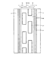
- FIG. 1 is a cross-sectional view showing a main part of a high voltage integrated circuit device according to a first embodiment of the present invention.
- FIG. 2 is a plan view showing a planar pattern of the first universal contact region.
- FIG. 3 is an explanatory diagram showing the behavior of electrons and holes when a negative surge voltage is applied via the H-VDD terminal.
- FIG. 4 is a cross-sectional view showing a main part of the high voltage integrated circuit device according to Embodiment 2 of the present invention.
- FIG. 5 is a plan view showing a planar pattern of the second universal contact region.
- FIG. 6 is an explanatory diagram showing the behavior of electrons and holes when a negative surge voltage is applied via the H-VDD terminal.
- FIG. 7 is a cross-sectional view showing the main parts of the high voltage integrated circuit device according to Embodiment 3 of the present invention.
- FIG. 8 is a cross-sectional view showing the main parts of the high voltage integrated circuit device according to Embodiment 4 of the present invention.
- FIG. 9 is an explanatory diagram showing a connection example of a switching power device that constitutes a power conversion device such as an inverter and a conventional HVIC that drives the switching power device.
- FIG. 10 is a circuit diagram showing the level-up circuit and its peripheral circuits.
- FIG. 11 is a circuit diagram showing a level-down circuit and its peripheral circuits.
- FIG. 12 is a circuit diagram showing in detail a level shift circuit of a conventional high voltage integrated circuit device.
- FIG. 13 is a cross-sectional view showing the main parts of the logic part of the high-side circuit part, the logic part of the low-side circuit part, and the level-up circuit part of the self-isolation type high voltage integrated circuit device.
- FIG. 14 is an explanatory diagram showing a malfunction of the low side circuit portion and the high side circuit portion of the conventional high voltage integrated circuit device.
- FIG. 15 is a plan view showing an example of the planar structure of the main part of the high voltage integrated circuit device of the present invention.
- FIG. 16 is a cross-sectional view showing another example of the main part of the high voltage integrated circuit device of the present invention.
- (Embodiment 1) 1 is a cross-sectional view showing a main part of a high voltage integrated circuit device according to a first embodiment of the present invention.
- an n region 3 serving as an n well region which is a high side floating potential region is formed on one main surface side (hereinafter referred to as a surface layer) inside the p semiconductor substrate 1.
- an n ⁇ region 4 to be a high breakdown voltage junction termination region 93 and an n ⁇ region 2 constituting an L-VDD potential region on the low side are formed.
- This high-voltage integrated circuit device 100 corresponds to the HVIC 111 that is the drive element shown in FIG. 9, and in particular, controls the IGBT 115 of the upper arm of the half bridge shown in FIG. 10 and the high-side circuit shown in FIG. It corresponds to the part. In FIG. 1, the level-up circuit is not shown. Further, the high-voltage integrated circuit device 100 can be provided with the level-down circuit shown in FIG. 11 as necessary.
- n region 3 which is the high side floating potential region
- a high side circuit portion 92 connected to a low voltage power source based on the intermediate potential Vs is formed as shown in FIGS.
- n ⁇ region 2 of the L-VDD potential region on the low side a low side circuit portion 91 connected to a GND-based low voltage power supply is formed as shown in FIGS.
- p region 61 is formed so as to surround n ⁇ region 4 and to be in contact with n region 3.
- a first universal contact region 58 is formed in which a p + region 56 and an n + region 57 are disposed in contact with each other along the surface of the p semiconductor substrate 1.
- the p region 61 is a fixed potential region for fixing the potential of the p semiconductor substrate 1 to the GND potential.
- the impurity concentration of p region 61 is higher than the impurity concentration of p semiconductor substrate 1 and lower than the impurity concentration of p + region 56.
- the first universal contact region 58 is in ohmic contact with the first pickup electrode 59 connected to the GND terminal.
- the first pickup electrode 59 and the first universal contact region 58 constitute a first universal contact structure.
- n + region 62 that is a contact region is formed in the surface layer of the n region 3.
- a second pickup electrode 69 that is in ohmic contact with the n + region 62 is formed.
- the n + region 62 is a fixed potential region for fixing to the potential on the high potential side of the power supply of the high side circuit section using the intermediate potential Vs as the reference potential.
- the impurity concentration of n + region 62 is higher than the impurity concentration of n region 3.
- the high breakdown voltage junction termination region 93 surrounds the n region 3 and the n ⁇ region 2 is arranged outside thereof.
- the low-side circuit unit 91 includes a first C-MOS circuit including a first p-channel MOSFET and a first n-channel MOSFET.
- the first p-channel MOSFET has a p + region 23 (source), a p + region 24 (drain), a first source electrode 81 and a first drain electrode 82.
- the first source electrode 81 is in ohmic contact with the p + region 23.
- the first drain electrode 82 is in ohmic contact with the p + region 24.
- the first n-channel MOSFET has an n + region 27 (source), an n + region 26 (drain), a second source electrode 83 and a second drain electrode 84.
- Second source electrode 83 is in ohmic contact with n + region 27.
- the second drain electrode 84 is in ohmic contact with the n + region 26.
- the high side circuit unit 92 includes a second C-MOS circuit including a second p-channel MOSFET and a second n-channel MOSFET.
- the second p-channel MOSFET has a p + region 33 (source), a p + region 34 (drain), a third source electrode 85 and a third drain electrode 86.
- Third source electrode 85 is in ohmic contact with p + region 33.
- Third drain electrode 86 is in ohmic contact with p + region 34.
- the second n-channel MOSFET has an n + region 37 (source), an n + region 36 (drain), a fourth source electrode 87, and a fourth drain electrode 88.
- the fourth source electrode 87 is in ohmic contact with the n + region 37.
- the fourth drain electrode 88 is in ohmic contact with the n + region 36.
- n + region 22, the p + region 28, the n + region 32, and the p + region 38 are contact regions, and the first source electrode 81, the second source electrode 83, the third source electrode 85, and the fourth source electrode 87. Each makes ohmic contact.
- the first pickup electrode 59 is connected to the second source electrode 83 and further connected to the GND terminal.
- the second pickup electrode 69 is connected to the third source electrode 85 and further connected to the H-VDD terminal.
- the first pickup electrode 59 is disposed on the low-side circuit portion 91 side of the high breakdown voltage junction termination region 93.
- the second pickup electrode 69 is disposed on the high-side circuit portion 92 side of the high breakdown voltage junction termination region 93.
- the first drain electrode 82 and the second drain electrode 84 are connected to each other and further connected to the L-OUT terminal.
- the third drain electrode 86 and the fourth drain electrode 88 are connected to each other, and further connected to the H-OUT terminal.
- phosphorus impurities or boron impurities are ion-implanted through a patterning step, and then, for example, a predetermined diffusion depth is formed in a diffusion step at a high temperature (about 1100 to 1200 ° C.). This is a well region that has been diffused.
- a p offset region serving as a base region is formed in the surface layer of the n ⁇ region 2 that is the L-VDD potential region in which the low side circuit portion 91 is formed.
- a first n-channel MOSFET is formed in the p region 21. Boron impurities are ion-implanted in this p region 21 through a patterning process, and then, for example, the n ⁇ regions 2, 4, n region 3 and p region 61 at a high temperature (about 1100 to 1200 ° C.) are formed. It diffuses to a predetermined diffusion depth in a diffusion process different from the diffusion process.
- n + region 62 that is a contact region for making ohmic contact with the H-VDD terminal, for example, arsenic is ion-implanted to a surface concentration of about 1 ⁇ 10 20 / cm 3 , and then, for example, 750 to 900 ° C. It is formed with a predetermined depth by a certain annealing process.
- the n + region 22 for making ohmic contact with the L-VDD terminal and the n + regions 27 and 26 of the source / drain of the first n-channel MOSFET constituting the low-side circuit unit 91 are also provided. It is formed by ion implantation and annealing. That is, through a patterning process for forming an n + region, for example, arsenic is ion-implanted so as to have a surface concentration of about 1 ⁇ 10 20 / cm 3 .
- the p + regions 23 and 24 that are the source and drain of the first p-channel MOSFET constituting the low side circuit portion 91 and the p + region 28 that is the contact region are also subjected to a patterning process for forming the p + region.
- a patterning process for forming the p + region For example, BF 2 is ion-implanted so that the surface concentration is about 1 ⁇ 10 20 / cm 3 .
- p + regions 23, 24, and 28 are formed with a predetermined diffusion depth by an annealing process of about 750 to 900 ° C., which is the same as described above.
- a p offset region (p region 31) that is a base region is formed on the surface layer of the n region 3 that is the high side floating potential region in which the high side circuit portion 92 is formed.
- a second n-channel MOSFET is formed in the p region 31.
- the p region 31 is formed in the same manner as the p region 21, for example.
- the n + region 32 for making ohmic contact with the H-VDD terminal and the n + regions 37 and 36 of the source / drain of the second n-channel MOSFET constituting the high side circuit portion 92 include n + regions 22, 27, 26.
- the p + regions 33 and 34 that are the source and drain of the second p-channel MOSFET constituting the high side circuit portion 92 and the p + region 38 that is the contact region are formed in the same manner as the p + regions 23, 24, and 28.
- FIG. 2 is a plan view showing a planar pattern of the first universal contact region shown in FIG.
- FIG. 2 shows a planar pattern of the first universal contact region 58 formed in the surface layer of the p region 61.
- the first universal contact region 58 includes a p + region 56 and an n + region 57 formed in the surface layer of the p region 61 constituting the parasitic pn diode 46.
- the p + region 56 and the n + region 57 are contact regions and are formed so as to be in contact with each other.
- the p + region 56 and the n + region 57 are formed using individual ion implantation masks.
- the n + region 57 at a deeper depth than the p + region 56 from the surface of the p + region 56 may be selectively formed.
- a first universal contact structure is formed on the first universal contact region 58 by bringing a metal electrode as the first pickup electrode 59 into ohmic contact.
- FIG. 2 shows a first universal contact region 58 having a planar layout in which a large number of n + regions 57 arranged in an island shape are disposed so as to be surrounded by the p + region 56. .
- n + compared to the p + region 56 It is desirable to increase the ratio of the region 57 or to form an n offset region described later in the fourth embodiment.
- n + regions 57 are alternately overlapped in the direction from the n + region 62 (H-VDD terminal) to the p region 61 in a short island shape instead of a line shape. It is desirable to arrange two or more layers (in FIG. 2, for example, a double structure).
- the planar shape of the n + region 57 arranged in an island shape may be a circle, a rectangle, or a polygon.
- the p + region 56 and the n + region 57 are formed in contact with each other in a stripe shape (for example, a stripe shape).
- the first universal contact region 58 is subjected to a patterning process using a planar pattern shown in FIG. 2, and the p + region 56 is individually ion-implanted so that, for example, BF 2 has a surface concentration of about 1 ⁇ 10 20 / cm 3. Ions are implanted using a mask. Subsequently, the n + region 57 is ion-implanted using, for example, an individual ion implantation mask so that arsenic has a surface concentration of about 1 ⁇ 10 20 / cm 3 .
- the p + region 56 and the n + region 57 are formed with a diffusion depth of about 0.2 ⁇ m to 0.5 ⁇ m by the same annealing process at about 750 ° C. to 900 ° C. as described above.
- the same annealing process at about 750 ° C. to 900 ° C. as described above.
- one impurity is not compensated by one impurity.
- FIG. 3 is an explanatory diagram showing the behavior of electrons and holes when a negative surge voltage is applied via the H-VDD terminal. Electrons are injected as minority carriers from the n ⁇ region 4 of the parasitic pn diode 46 composed of the p region 61 and the n ⁇ region 4 into the p region 61, and the electrons flow into the n ⁇ region 2 through the p region 61. At this time, some of the electrons that have entered the p region 61 in the middle of the movement path of electrons flowing from the n ⁇ region 4 to the n ⁇ region 2 have a higher junction barrier (about 0.6 V higher) than the p region 61. That is, it is trapped in the n + region 57 having a low electron energy barrier and extracted by the first pickup electrode 59.
- the amount of electrons flowing into the n ⁇ region 2 is reduced, so that malfunction of the logic part of the low-side circuit part 91 and destruction due to latch-up can be prevented.
- the amount of holes emitted from the p + region 56 of the first universal contact region 58 to the p region 61 is suppressed because the n + region 57 is adjacent to the p + region 56. Therefore, the amount of holes injected from the p region 61 of the parasitic pn diode 46 to the n ⁇ region 4 is also reduced, and the malfunction of the logic portion of the high side circuit portion 92 and the breakdown due to latch-up can be prevented.
- the area required for forming the first universal contact region 58 is the same as the area of the p + region 56 which is the conventional first contact region shown in FIG. For this reason, the chip size does not increase and the manufacturing cost does not increase.
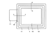
- FIG. 15 is a plan view showing an example of the planar structure of the main part of the high voltage integrated circuit device of the present invention.
- the cross-sectional structure taken along section line AA corresponds to the cross-sectional view shown in FIG.
- the cross-sectional structure taken along the cutting line BB corresponds to the cross-sectional view shown in FIG.
- the first universal contact region 58 is formed with the same planar layout.
- the n + region 62 that is the second contact region is formed over the entire circumference so as to surround the high side circuit portion 92, but may not be formed over the entire circumference.
- the n + region 62 is at least between the C-MOS circuit of the high side circuit portion 92 and the high breakdown voltage junction termination region. It is desirable to provide it.
- the n + region 62 is formed with the same planar layout.
- FIG. 16 is a cross-sectional view showing another example of the main part of the high voltage integrated circuit device of the present invention.
- a high voltage integrated circuit device 100 shown in FIG. 16 is manufactured using an epitaxial substrate in which an n epitaxial growth layer (n epi) is formed on a p support substrate.
- n epi n epitaxial growth layer
- a p region 61 that penetrates the n epitaxial growth layer and reaches the p support substrate is formed, and a first universal contact region 58 composed of a p + region 56 and an n + region 57 is formed in the surface layer. Is done.
- the high voltage integrated circuit device according to the following second to fourth embodiments may be a high voltage integrated circuit device manufactured using an epitaxial substrate.
- the first universal contact region 58 is formed as the pickup region fixed to the GND potential outside the high breakdown voltage junction termination region 93 surrounding the high side circuit portion 92.
- the amount of carriers flowing into the low-side circuit unit 91 can be reduced, and the logic unit of the low-side circuit unit 91 can be prevented from malfunctioning or being destroyed due to latch-up.
- FIG. 4 is a cross-sectional view showing a main part of the high voltage integrated circuit device according to Embodiment 2 of the present invention.
- the high voltage integrated circuit device 200 according to the second embodiment is different from the high voltage integrated circuit device 100 according to the first embodiment of FIG. 1 in that the second voltage is also below the second pickup electrode 69 to which the H-VDD terminal is connected.
- the universal contact region 68 is formed.
- Second universal contact region 68 includes n + regions 62 and p + regions 63 that are alternately arranged in contact with each other along the surface of p semiconductor substrate 1.
- the plane pattern of the first universal contact region 58 is the same as the plane pattern (FIG. 2) of the first universal contact region of the first embodiment.
- FIG. 5 is a plan view showing a planar pattern of the second universal contact region.
- the second universal contact region 68 has a rectangular planar shape so as to be surrounded by the n + region 62 and has a planar layout in which a large number of p + regions 63 arranged in an island shape are disposed.
- the planar shape of the p + region 63 arranged in an island shape may be a circle, a rectangle, or a polygon.
- the p + region 63 and the n + region 62 are formed in contact with each other in a stripe shape (for example, a stripe shape).
- the second universal contact region 68 that is in ohmic contact with the H-VDD terminal is subjected to the patterning process using the planar pattern shown in FIG. 5 to form the n + region 62 with, for example, arsenic having a surface concentration of about 1 ⁇ 10 20 / cm 3 . Ion implantation is performed. Subsequently, for example, BF 2 is ion-implanted into the p + region 63 so as to have a surface concentration of about 1 ⁇ 10 20 / cm 3 . Thereafter, the second universal contact region 68 is formed by diffusion at a depth of about 0.2 ⁇ m to 0.5 ⁇ m in an annealing process of about 750 ° C. to 900 ° C., for example.
- FIG. 6 is an explanatory diagram showing the behavior of electrons and holes when a negative surge voltage is applied via the H-VDD terminal. Since there is a p + region 63 adjacent to the n + region 62 of the second universal contact region 68, the current flowing through the parasitic pn diode 46 composed of the p region 61 and the n ⁇ region 4 out of the n + region 62 to n. - the amount of electrons emitted into the region 4 is suppressed. Therefore, the amount of electrons injected from n ⁇ region 4 into p region 61 is reduced.
- the electrons that have entered the p region 61 are extracted from the n + region 57 constituting the first universal contact region 58. For this reason, the amount of electrons entering the n ⁇ region 2 is smaller than that of the high voltage integrated circuit device 100 of FIG. As a result, it is possible to further prevent the malfunction of the logic part of the low side circuit part 91 and the breakdown due to the latch-up.
- p region 61 and n - flows into the n region 3 through the space 4 - from p region 61 of the parasitic pn diode 46 consisting of region 4 which n - holes as minority carriers are injected into the region 4, the n .
- some of the holes are trapped in the p + region 63 having a higher junction barrier (about 0.6 V higher) than the n region 3 and extracted by the second pickup electrode 69.
- the amount of holes emitted from the p + region 56 of the first universal contact region 58 to the p region 61 is suppressed because the n + region 57 is adjacent to the p + region 56. Therefore, the amount of holes injected from the p region 61 of the parasitic pn diode 46 to the n ⁇ region 4 is also reduced, and malfunction of the logic unit of the high side circuit unit 92 and destruction due to latch-up can be prevented.
- the area necessary for forming the first universal contact region 58 and the second universal contact region 68 is p + region 56 which is the conventional first contact region and n which is the second contact region shown in FIG.
- the area of the + region 62 is the same. For this reason, the chip size does not increase and the manufacturing cost does not increase.
- the second universal contact region 68 is formed as a pickup region that is disposed on the outer peripheral portion of the high side circuit portion 92 and is fixed to the potential on the high potential side of the power source of the high side circuit portion 92, thereby forming the low side circuit portion.
- the amount of carriers flowing into 91 can be reduced, and the malfunction of the logic part of the low side circuit part 91 and the breakdown due to latch-up can be prevented.
- FIG. 7 is a cross-sectional view showing the main parts of the high voltage integrated circuit device according to Embodiment 3 of the present invention.
- the high voltage integrated circuit device 300 according to the third embodiment is different from the high voltage integrated circuit device 200 according to the second embodiment in FIG. 4 in that only the second universal contact region 68 is formed, and the first universal contact region 58 is formed. Is not formed.
- the second universal contact region 68 By forming the second universal contact region 68, when a negative surge voltage is applied to the HVDD terminal via the Vs terminal, as described with reference to FIG. 6 in the second embodiment, the p region 61 The amount of electrons injected into the substrate is reduced. As a result, the amount of electrons flowing into the n ⁇ region 2 is reduced, and malfunction and destruction of the logic part of the low side circuit part 91 can be prevented.
- the area required for forming the second universal contact region 68 is the same as the area of the n + region 62 which is the conventional second contact region of FIG. For this reason, the chip size does not increase and the manufacturing cost does not increase.
- FIG. 8 is a cross-sectional view showing the main parts of the high voltage integrated circuit device according to Embodiment 4 of the present invention.
- the high voltage integrated circuit device 400 according to the fourth embodiment is different from the high voltage integrated circuit device 100 according to the first embodiment of FIG. 1 in that the p + is replaced with the n + region 57 of the first universal contact region 58.
- the third universal contact region 98 having the n offset region 97 having a diffusion depth deeper than the region 56 is formed.
- the n offset region 97 penetrates the p region 61 and reaches the p semiconductor substrate 1.
- This n offset region 97 is, for example, a high temperature (about 1100 to 1200 ° C.) diffusion process for forming the p region 21 which is a p offset region, or high acceleration ion implantation of about 1 MeV and driving of the n + region 57. It is formed with a diffusion depth of about 0.6 ⁇ m to 5 ⁇ m by the same annealing process of about 750 ° C. to 900 ° C. as in the process.
- n offset region 97 By providing this n offset region 97, when a negative surge voltage is input, electrons which are minority carriers flowing through the parasitic pn diode 46 composed of the p region 61 and the n ⁇ region 4 are efficiently trapped in the n offset region 97. Thus, the amount of electrons flowing into the logic part (n ⁇ region 2) of the low side circuit part 91 can be effectively reduced.
- the present invention is not limited to the first to fourth embodiments described above, but a high-breakdown-voltage n-channel MOSFET which is a logic unit or level shifter element of an internal power supply circuit (internal reference voltage circuit) set lower than the L-VDD potential. This is also effective in the logic section of a pulse generator circuit for driving the gates of the first and second gates. In the present invention, these circuits are included in the low-side circuit unit 91.
- the high voltage integrated circuit device is a high voltage integrated circuit used for transmitting an on / off drive signal to the gate of a power device in, for example, a PWM inverter, a switching power supply or the like. It is useful for a device, and in particular, prevents malfunction caused by an overcurrent flowing in a circuit.
Abstract
Description
図1は、この発明の実施の形態1にかかる高耐圧集積回路装置の要部を示す断面図である。図1に示す高耐圧集積回路装置100において、p半導体基板1の内部の一方の主面側(以下、表面層とする)には、ハイサイド浮遊電位領域であるnウェル領域となるn領域3と、高耐圧接合終端領域93となるn-領域4と、ローサイド側のL-VDD電位領域を構成するn-領域2とが形成されている。 (Embodiment 1)
1 is a cross-sectional view showing a main part of a high voltage integrated circuit device according to a first embodiment of the present invention. In the high withstand voltage integrated
図4は、この発明の実施の形態2にかかる高耐圧集積回路装置の要部を示す断面図である。実施の形態2にかかる高耐圧集積回路装置200が図1の実施の形態1にかかる高耐圧集積回路装置100と異なるのは、H-VDD端子が接続する第2ピックアップ電極69下にも第2ユニバーサルコンタクト領域68が形成されている点である。第2ユニバーサルコンタクト領域68は、p半導体基板1の表面に沿って互いに接して交互に配置されるn+領域62とp+領域63とからなる。尚、説明を省略するが、第1ユニバーサルコンタクト領域58の平面パターンは、実施の形態1の第1ユニバーサルコンタクト領域の平面パターン(図2)と同じである。 (Embodiment 2)
FIG. 4 is a cross-sectional view showing a main part of the high voltage integrated circuit device according to
図7は、この発明の実施の形態3にかかる高耐圧集積回路装置の要部を示す断面図である。実施の形態3にかかる高耐圧集積回路装置300が図4の実施の形態2にかかる高耐圧集積回路装置200と異なるのは、第2ユニバーサルコンタクト領域68のみを形成し、第1ユニバーサルコンタクト領域58を形成していない点である。 (Embodiment 3)
FIG. 7 is a cross-sectional view showing the main parts of the high voltage integrated circuit device according to
図8は、この発明の実施の形態4にかかる高耐圧集積回路装置の要部を示す断面図である。実施の形態4にかかる高耐圧集積回路装置400が図1の実施の形態1にかかる高耐圧集積回路装置100と異なるのは、第1ユニバーサルコンタクト領域58のn+領域57に代えて、p+領域56よりも拡散深さが深いnオフセット領域97を有する第3ユニバーサルコンタクト領域98を形成した点である。nオフセット領域97は、p領域61を貫通しp半導体基板1に達する。 (Embodiment 4)
FIG. 8 is a cross-sectional view showing the main parts of the high voltage integrated circuit device according to
2,4 n-領域
3 n領域
21,61 p領域
22,26,27,32,36,37,57,62 n+領域
23,24,28,33,34,38,56,63 p+領域
58 第1ユニバーサルコンタクト領域
59 第1ピックアップ電極
68 第2ユニバーサルコンタクト領域
69 第2ピックアップ電極
81 第1ソース電極
82 第1ドレイン電極
83 第2ソース電極
84 第2ドレイン電極
85 第3ソース電極
86 第3ドレイン電極
87 第4ソース電極
88 第4ドレイン電極
91 ローサイド回路部
92 ハイサイド回路部
93 高耐圧接合終端領域
97 nオフセット領域
98 第3ユニバーサルコンタクト領域
100,200,300,400 高耐圧集積回路装置 1
Claims (7)
- 第1導電型の半導体基板と、
前記半導体基板上に配置された、GND電位を基準とする低電圧電源に接続された第2導電型のローサイド回路部と、
前記半導体基板上に前記ローサイド回路部と離れて配置された、GND電位よりも高い中間電位を基準とする低電圧電源に接続される第2導電型のハイサイド回路部と、
GND電位に電気的に接続され、かつ前記ハイサイド回路部を取り囲んで配置され、前記ローサイド回路部の外周部と共に高耐圧接合終端領域を形成する第1導電型領域と、
前記第1導電型領域に配置された第1ピックアップ電極と、
前記高耐圧接合終端領域の内側であって前記ハイサイド回路部の外周部に配置され、前記中間電位を基準とする低電圧電源の高電位側に接続された第2ピックアップ電極と、
前記第1ピックアップ電極にオーミック接触する第1導電型の第1高濃度コンタクト領域と、
前記第2ピックアップ電極にオーミック接触する第2導電型の第2高濃度コンタクト領域と、
を備え、
前記第1高濃度コンタクト領域および前記第2高濃度コンタクト領域の少なくとも一方の領域が、前記半導体基板の表面に沿ってp領域とn領域とが互いに接して交互に配置された構成のユニバーサルコンタクト領域であることを特徴とする高耐圧集積回路装置。 A first conductivity type semiconductor substrate;
A low-side circuit portion of a second conductivity type disposed on the semiconductor substrate and connected to a low-voltage power source based on the GND potential;
A second-conductivity-type high-side circuit portion connected to a low-voltage power source with an intermediate potential higher than the GND potential disposed on the semiconductor substrate apart from the low-side circuit portion;
A first conductivity type region that is electrically connected to a GND potential and is disposed so as to surround the high-side circuit unit and forms a high-breakdown-voltage junction termination region together with an outer peripheral portion of the low-side circuit unit;
A first pickup electrode disposed in the first conductivity type region;
A second pickup electrode disposed inside the high withstand voltage junction termination region and at an outer peripheral portion of the high side circuit portion, and connected to a high potential side of a low voltage power source based on the intermediate potential;
A first high-concentration contact region of a first conductivity type in ohmic contact with the first pickup electrode;
A second high-concentration contact region of a second conductivity type in ohmic contact with the second pickup electrode;
With
A universal contact region having a configuration in which at least one of the first high-concentration contact region and the second high-concentration contact region is alternately arranged with p regions and n regions in contact with each other along the surface of the semiconductor substrate A high voltage integrated circuit device characterized by the above. - 第1導電型の半導体基板と、
前記半導体基板上に配置されたローサイド回路部を備えた第2導電型の第1半導体領域と、
前記半導体基板上に前記第1半導体領域と離れて配置されたハイサイド回路部を備えた第2導電型の第2半導体領域と、
前記第1半導体領域の表面層に配置された第1導電型のソース領域および第1導電型のドレイン領域を有する第1MOSFETと、前記第1半導体領域の表面層に前記第1MOSFETと離れて配置された第1導電型の第3半導体領域と、前記第3半導体領域の表面層に配置された第2導電型のソース領域および第2導電型のドレイン領域を有する第2MOSFETと、からなる第1C-MOS回路と、
前記第2半導体領域の表面層に配置された第1導電型のソース領域および第1導電型のドレイン領域を有する第3MOSFETと、前記第2半導体領域の表面層に前記第3MOSFETと離れて配置された第1導電型の第4半導体領域と、前記第4半導体領域の表面層に配置された第2導電型のソース領域および第2導電型のドレイン領域を有する第4MOSFETと、からなる第2C-MOS回路と、
前記半導体基板の表面層に配置され前記第2半導体領域を囲み、前記半導体基板より高不純物濃度の第1導電型の第5半導体領域と、
前記第5半導体領域の表面層に配置された、前記第5半導体領域より高不純物濃度の第1導電型の第1コンタクト領域と、
前記第5半導体領域と前記第2半導体領域の外周部とにより構成される高耐圧接合終端領域と、
前記第2半導体領域の表面層であって前記高耐圧接合終端領域の内側に配置された、前記第2半導体領域より高不純物濃度の第2導電型の第2コンタクト領域と、
前記第1半導体領域の表面層に配置され、前記第1MOSFETのソース領域と接する第2導電型の第3コンタクト領域と、
前記第3半導体領域の表面層に配置され、前記第2MOSFETのソース領域と接する第1導電型の第4コンタクト領域と、
前記第2半導体領域の表面層に配置され、前記第3MOSFETのソース領域と接する第2導電型の第5コンタクト領域と、
前記第4半導体領域の表面層に配置され、前記第4MOSFETのソース領域と接する第1導電型の第6コンタクト領域と、
前記第1コンタクト領域上に配置され当該第1コンタクト領域とオーミック接触する第1ピックアップ電極と、
前記第2コンタクト領域上に配置され当該第2コンタクト領域とオーミック接触する第2ピックアップ電極と、
前記第1MOSFETのソース領域および第3コンタクト領域に接する第1ソース電極と、
前記第1MOSFETのドレイン領域に接する第1ドレイン電極と、
前記第2MOSFETのソース領域および第4コンタクト領域に接する第2ソース電極と、
前記第2MOSFETのドレイン領域に接する第2ドレイン電極と、
前記第3MOSFETのソース領域および第5コンタクト領域に接する第3ソース電極と、
前記第3MOSFETのドレイン領域に接する第3ドレイン電極と、
前記第4MOSFETのソース領域および第6コンタクト領域に接する第4ソース電極と、
前記第4MOSFETのドレイン領域に接する第4ドレイン電極と、
前記第2ソース電極および前記第1ピックアップ電極が接続されたGND端子と、
前記第3ソース電極および前記第2ピックアップ電極が接続された高電位側端子と、
を備え、
前記第1コンタクト領域および前記第2コンタクト領域の少なくとも一方の領域が、前記半導体基板の表面に沿ってp領域とn領域とが互いに接して交互に配置された構成のユニバーサルコンタクト領域であることを特徴とする高耐圧集積回路装置。 A first conductivity type semiconductor substrate;
A first semiconductor region of a second conductivity type having a low side circuit portion disposed on the semiconductor substrate;
A second conductivity type second semiconductor region comprising a high side circuit portion disposed on the semiconductor substrate apart from the first semiconductor region;
A first MOSFET having a first conductivity type source region and a first conductivity type drain region disposed in a surface layer of the first semiconductor region; and being disposed apart from the first MOSFET in a surface layer of the first semiconductor region. A first conductivity type third semiconductor region, and a second MOSFET having a second conductivity type source region and a second conductivity type drain region disposed in a surface layer of the third semiconductor region. A MOS circuit;
A third MOSFET having a first conductivity type source region and a first conductivity type drain region disposed on a surface layer of the second semiconductor region; and a third MOSFET disposed on a surface layer of the second semiconductor region apart from the third MOSFET. And a second MOSFET having a first conductivity type fourth semiconductor region and a fourth MOSFET having a second conductivity type source region and a second conductivity type drain region disposed in a surface layer of the fourth semiconductor region. A MOS circuit;
A fifth semiconductor region of a first conductivity type disposed on a surface layer of the semiconductor substrate, surrounding the second semiconductor region, and having a higher impurity concentration than the semiconductor substrate;
A first contact region of a first conductivity type having a higher impurity concentration than the fifth semiconductor region, disposed in a surface layer of the fifth semiconductor region;
A high-breakdown-voltage junction termination region constituted by the fifth semiconductor region and the outer periphery of the second semiconductor region;
A second contact region of a second conductivity type having a higher impurity concentration than the second semiconductor region, disposed on the inner surface of the high-breakdown-voltage junction termination region on the surface layer of the second semiconductor region;
A third contact region of a second conductivity type disposed in a surface layer of the first semiconductor region and in contact with a source region of the first MOSFET;
A fourth contact region of a first conductivity type disposed on a surface layer of the third semiconductor region and in contact with a source region of the second MOSFET;
A fifth contact region of a second conductivity type disposed in a surface layer of the second semiconductor region and in contact with a source region of the third MOSFET;
A sixth contact region of a first conductivity type disposed on a surface layer of the fourth semiconductor region and in contact with a source region of the fourth MOSFET;
A first pickup electrode disposed on the first contact region and in ohmic contact with the first contact region;
A second pickup electrode disposed on the second contact region and in ohmic contact with the second contact region;
A first source electrode in contact with a source region and a third contact region of the first MOSFET;
A first drain electrode in contact with a drain region of the first MOSFET;
A second source electrode in contact with a source region and a fourth contact region of the second MOSFET;
A second drain electrode in contact with the drain region of the second MOSFET;
A third source electrode in contact with a source region and a fifth contact region of the third MOSFET;
A third drain electrode in contact with the drain region of the third MOSFET;
A fourth source electrode in contact with a source region and a sixth contact region of the fourth MOSFET;
A fourth drain electrode in contact with the drain region of the fourth MOSFET;
A GND terminal to which the second source electrode and the first pickup electrode are connected;
A high potential side terminal to which the third source electrode and the second pickup electrode are connected;
With
At least one of the first contact region and the second contact region is a universal contact region having a configuration in which p regions and n regions are alternately arranged in contact with each other along the surface of the semiconductor substrate. High voltage integrated circuit device characterized. - 前記ユニバーサルコンタクト領域を構成する前記p領域および前記n領域のうちの一方の領域が他方の領域に囲まれていることを特徴とする請求項1または2に記載の高耐圧集積回路装置。 3. The high breakdown voltage integrated circuit device according to claim 1, wherein one of the p region and the n region constituting the universal contact region is surrounded by the other region.
- 前記ユニバーサルコンタクト領域を構成する前記p領域および前記n領域の平面形状が共に帯状であることを特徴とする請求項1または2に記載の高耐圧集積回路装置。 The high withstand voltage integrated circuit device according to claim 1 or 2, wherein the planar shape of the p region and the n region constituting the universal contact region are both strips.
- 前記ユニバーサルコンタクト領域を構成する前記p領域および前記n領域のうちの、前記第1導電型領域の導電型と異なる導電型の領域の深さは、前記第1導電型領域の深さ以上の深さであることを特徴とする請求項1に記載の高耐圧集積回路装置。 Of the p region and the n region constituting the universal contact region, the depth of a region of a conductivity type different from the conductivity type of the first conductivity type region is greater than the depth of the first conductivity type region. The high withstand voltage integrated circuit device according to claim 1, wherein
- 前記ユニバーサルコンタクト領域を構成する前記p領域および前記n領域のうちの、前記第5半導体領域の導電型と異なる導電型の領域の深さは、前記第5半導体領域の深さ以上の深さであることを特徴とする請求項2に記載の高耐圧集積回路装置。 Of the p region and the n region constituting the universal contact region, the depth of the region having a conductivity type different from the conductivity type of the fifth semiconductor region is greater than the depth of the fifth semiconductor region. The high voltage integrated circuit device according to claim 2, wherein the high voltage integrated circuit device is provided.
- 前記ハイサイド回路部は、ハーフブリッジ回路を構成する上アームのスイッチング素子および下アームのスイッチング素子の接続点を基準電位とする電源に接続された、前記上アームのスイッチング素子を駆動するための回路部であり、
前記高電位側端子は、前記電源の高電位側に接続され、
前記GND端子は、GND電位に接続されていることを特徴とする請求項2に記載の高耐圧集積回路装置。 The high-side circuit unit is a circuit for driving the switching element of the upper arm connected to a power source having a reference potential at a connection point of the switching element of the upper arm and the switching element of the lower arm constituting the half bridge circuit. Department,
The high potential side terminal is connected to the high potential side of the power source,
The high withstand voltage integrated circuit device according to claim 2, wherein the GND terminal is connected to a GND potential.
Priority Applications (4)
| Application Number | Priority Date | Filing Date | Title |
|---|---|---|---|
| CN201280001968.5A CN102986027B (en) | 2011-03-15 | 2012-03-13 | High voltage integrated circuit equipment |
| JP2012532398A JP5099282B1 (en) | 2011-03-15 | 2012-03-13 | High voltage integrated circuit device |
| EP12757637.9A EP2581938B1 (en) | 2011-03-15 | 2012-03-13 | High-voltage integrated circuit device |
| US13/738,652 US8633563B2 (en) | 2011-03-15 | 2013-01-10 | High-voltage integrated circuit device |
Applications Claiming Priority (2)
| Application Number | Priority Date | Filing Date | Title |
|---|---|---|---|
| JP2011056577 | 2011-03-15 | ||
| JP2011-056577 | 2011-03-15 |
Related Child Applications (1)
| Application Number | Title | Priority Date | Filing Date |
|---|---|---|---|
| US13/738,652 Continuation US8633563B2 (en) | 2011-03-15 | 2013-01-10 | High-voltage integrated circuit device |
Publications (1)
| Publication Number | Publication Date |
|---|---|
| WO2012124677A1 true WO2012124677A1 (en) | 2012-09-20 |
Family
ID=46830744
Family Applications (1)
| Application Number | Title | Priority Date | Filing Date |
|---|---|---|---|
| PCT/JP2012/056373 WO2012124677A1 (en) | 2011-03-15 | 2012-03-13 | High-voltage integrated circuit device |
Country Status (5)
| Country | Link |
|---|---|
| US (1) | US8633563B2 (en) |
| EP (1) | EP2581938B1 (en) |
| JP (1) | JP5099282B1 (en) |
| CN (1) | CN102986027B (en) |
| WO (1) | WO2012124677A1 (en) |
Cited By (5)
| Publication number | Priority date | Publication date | Assignee | Title |
|---|---|---|---|---|
| WO2015029456A1 (en) * | 2013-09-02 | 2015-03-05 | 富士電機株式会社 | Semiconductor device |
| JP2015065274A (en) * | 2013-09-25 | 2015-04-09 | 株式会社デンソー | Junction isolation semiconductor integrated circuit and manufacturing method of the same |
| JP2016004883A (en) * | 2014-06-16 | 2016-01-12 | 富士電機株式会社 | Semiconductor integrated circuit device |
| JP2017045966A (en) * | 2015-08-28 | 2017-03-02 | ルネサスエレクトロニクス株式会社 | Semiconductor device |
| TWI629785B (en) * | 2016-12-29 | 2018-07-11 | 新唐科技股份有限公司 | High voltage junction terminating structure of high voltage integrated circuit |
Families Citing this family (8)
| Publication number | Priority date | Publication date | Assignee | Title |
|---|---|---|---|---|
| US9502401B2 (en) | 2013-08-16 | 2016-11-22 | Infineon Technologies Austria Ag | Integrated circuit with first and second switching devices, half bridge circuit and method of manufacturing |
| US20150236090A1 (en) * | 2014-02-14 | 2015-08-20 | Nxp B.V. | Transistor with reducted parasitic |
| JP6413467B2 (en) * | 2014-08-19 | 2018-10-31 | 富士電機株式会社 | Semiconductor device |
| US9698147B2 (en) * | 2015-02-25 | 2017-07-04 | Sii Semiconductor Corporation | Semiconductor integrated circuit device having low and high withstanding-voltage MOS transistors |
| TWI576981B (en) * | 2015-06-25 | 2017-04-01 | 聯華電子股份有限公司 | Semiconductor structure suitable for electrostatic discharge protection application |
| JP6972691B2 (en) * | 2017-06-19 | 2021-11-24 | 富士電機株式会社 | Semiconductor devices and methods for manufacturing semiconductor devices |
| US10636872B1 (en) * | 2018-10-31 | 2020-04-28 | Globalfoundries Inc. | Apparatus and method to prevent integrated circuit from entering latch-up mode |
| CN111326578B (en) * | 2018-12-13 | 2022-08-02 | 中芯集成电路(宁波)有限公司 | Gate drive integrated circuit |
Citations (8)
| Publication number | Priority date | Publication date | Assignee | Title |
|---|---|---|---|---|
| JPH11214532A (en) * | 1998-01-27 | 1999-08-06 | Matsushita Electric Works Ltd | Semiconductor device |
| JP2001025235A (en) | 1999-07-07 | 2001-01-26 | Mitsubishi Electric Corp | Driving gear and power converter |
| JP3346763B2 (en) | 1999-11-24 | 2002-11-18 | インターナショナル・レクチファイヤー・コーポレーション | High voltage integrated circuit chip |
| JP2005175454A (en) * | 2003-11-19 | 2005-06-30 | Matsushita Electric Ind Co Ltd | Sustaining driver of plasma display, and its control circuit |
| JP2005252235A (en) * | 2004-02-04 | 2005-09-15 | Matsushita Electric Ind Co Ltd | Semiconductor device |
| JP2006140302A (en) * | 2004-11-12 | 2006-06-01 | Matsushita Electric Ind Co Ltd | Drive circuit and data line driver |
| JP2008301160A (en) | 2007-05-31 | 2008-12-11 | Fuji Electric Device Technology Co Ltd | Level shift circuit and semiconductor device |
| JP2009147378A (en) | 2009-03-24 | 2009-07-02 | Mitsubishi Electric Corp | Semiconductor device |
Family Cites Families (13)
| Publication number | Priority date | Publication date | Assignee | Title |
|---|---|---|---|---|
| JP3808116B2 (en) * | 1995-04-12 | 2006-08-09 | 富士電機デバイステクノロジー株式会社 | High voltage IC |
| JP4068746B2 (en) * | 1998-12-25 | 2008-03-26 | 株式会社ルネサステクノロジ | Semiconductor integrated circuit device |
| CN1171317C (en) * | 1999-04-30 | 2004-10-13 | 罗姆股份有限公司 | Semicondcutor device having bipolar transistors |
| EP1368875A1 (en) * | 2001-03-16 | 2003-12-10 | Sarnoff Corporation | Electrostatic discharge protection structures having high holding current for latch-up immunity |
| US6576959B2 (en) * | 2001-04-10 | 2003-06-10 | Texas Instruments Incorporated | Device and method of low voltage SCR protection for high voltage failsafe ESD applications |
| US6444511B1 (en) * | 2001-05-31 | 2002-09-03 | Taiwan Semiconductor Manufacturing Company | CMOS output circuit with enhanced ESD protection using drain side implantation |
| JP3951815B2 (en) * | 2001-06-11 | 2007-08-01 | 富士電機デバイステクノロジー株式会社 | Semiconductor device |
| US8513087B2 (en) * | 2002-08-14 | 2013-08-20 | Advanced Analogic Technologies, Incorporated | Processes for forming isolation structures for integrated circuit devices |
| US20060220168A1 (en) * | 2005-03-08 | 2006-10-05 | Monolithic Power Systems, Inc. | Shielding high voltage integrated circuits |
| JP2007081009A (en) * | 2005-09-13 | 2007-03-29 | Matsushita Electric Ind Co Ltd | Drive circuit and data line driver |
| JP5431255B2 (en) | 2009-07-02 | 2014-03-05 | 信越化学工業株式会社 | Antifoam |
| KR101060128B1 (en) * | 2009-09-11 | 2011-08-29 | (주) 트리노테크놀로지 | MOS gate power semiconductor device |
| US8476736B2 (en) * | 2011-02-18 | 2013-07-02 | Taiwan Semiconductor Manufacturing Company, Ltd. | Low leakage diodes |
-
2012
- 2012-03-13 CN CN201280001968.5A patent/CN102986027B/en active Active
- 2012-03-13 WO PCT/JP2012/056373 patent/WO2012124677A1/en active Application Filing
- 2012-03-13 JP JP2012532398A patent/JP5099282B1/en active Active
- 2012-03-13 EP EP12757637.9A patent/EP2581938B1/en active Active
-
2013
- 2013-01-10 US US13/738,652 patent/US8633563B2/en active Active
Patent Citations (8)
| Publication number | Priority date | Publication date | Assignee | Title |
|---|---|---|---|---|
| JPH11214532A (en) * | 1998-01-27 | 1999-08-06 | Matsushita Electric Works Ltd | Semiconductor device |
| JP2001025235A (en) | 1999-07-07 | 2001-01-26 | Mitsubishi Electric Corp | Driving gear and power converter |
| JP3346763B2 (en) | 1999-11-24 | 2002-11-18 | インターナショナル・レクチファイヤー・コーポレーション | High voltage integrated circuit chip |
| JP2005175454A (en) * | 2003-11-19 | 2005-06-30 | Matsushita Electric Ind Co Ltd | Sustaining driver of plasma display, and its control circuit |
| JP2005252235A (en) * | 2004-02-04 | 2005-09-15 | Matsushita Electric Ind Co Ltd | Semiconductor device |
| JP2006140302A (en) * | 2004-11-12 | 2006-06-01 | Matsushita Electric Ind Co Ltd | Drive circuit and data line driver |
| JP2008301160A (en) | 2007-05-31 | 2008-12-11 | Fuji Electric Device Technology Co Ltd | Level shift circuit and semiconductor device |
| JP2009147378A (en) | 2009-03-24 | 2009-07-02 | Mitsubishi Electric Corp | Semiconductor device |
Non-Patent Citations (1)
| Title |
|---|
| See also references of EP2581938A4 |
Cited By (13)
| Publication number | Priority date | Publication date | Assignee | Title |
|---|---|---|---|---|
| US9793886B2 (en) | 2013-09-02 | 2017-10-17 | Fuji Electric Co., Ltd. | Semiconductor device for high-voltage circuit |
| CN105190866A (en) * | 2013-09-02 | 2015-12-23 | 富士电机株式会社 | Semiconductor device |
| WO2015029456A1 (en) * | 2013-09-02 | 2015-03-05 | 富士電機株式会社 | Semiconductor device |
| US10396775B2 (en) | 2013-09-02 | 2019-08-27 | Fuji Electric Co., Ltd. | Semiconductor device for high-voltage circuit |
| JP5987991B2 (en) * | 2013-09-02 | 2016-09-07 | 富士電機株式会社 | Semiconductor device |
| JPWO2015029456A1 (en) * | 2013-09-02 | 2017-03-02 | 富士電機株式会社 | Semiconductor device |
| JP2015065274A (en) * | 2013-09-25 | 2015-04-09 | 株式会社デンソー | Junction isolation semiconductor integrated circuit and manufacturing method of the same |
| JP2016004883A (en) * | 2014-06-16 | 2016-01-12 | 富士電機株式会社 | Semiconductor integrated circuit device |
| CN105321944B (en) * | 2014-06-16 | 2019-07-05 | 富士电机株式会社 | Conductor integrated circuit device |
| CN105321944A (en) * | 2014-06-16 | 2016-02-10 | 富士电机株式会社 | Semiconductor integrated circuit |
| JP2017045966A (en) * | 2015-08-28 | 2017-03-02 | ルネサスエレクトロニクス株式会社 | Semiconductor device |
| TWI629785B (en) * | 2016-12-29 | 2018-07-11 | 新唐科技股份有限公司 | High voltage junction terminating structure of high voltage integrated circuit |
| US10573713B2 (en) | 2016-12-29 | 2020-02-25 | Nuvoton Technology Corporation | High voltage junction terminating structure of high voltage integrated circuit |
Also Published As
| Publication number | Publication date |
|---|---|
| EP2581938A1 (en) | 2013-04-17 |
| JPWO2012124677A1 (en) | 2014-07-24 |
| EP2581938A4 (en) | 2014-12-31 |
| US8633563B2 (en) | 2014-01-21 |
| JP5099282B1 (en) | 2012-12-19 |
| EP2581938B1 (en) | 2020-01-08 |
| US20130127524A1 (en) | 2013-05-23 |
| CN102986027A (en) | 2013-03-20 |
| CN102986027B (en) | 2016-03-02 |
Similar Documents
| Publication | Publication Date | Title |
|---|---|---|
| JP5099282B1 (en) | High voltage integrated circuit device | |
| US9478543B2 (en) | Semiconductor integrated circuit | |
| JP6447139B2 (en) | High voltage integrated circuit device | |
| US8704328B2 (en) | High-voltage integrated circuit device | |
| JP5757145B2 (en) | Semiconductor device | |
| US9412732B2 (en) | Semiconductor device | |
| JP6237901B2 (en) | Semiconductor integrated circuit device | |
| JP5435138B2 (en) | High voltage integrated circuit device | |
| TWI557876B (en) | Semiconductor device | |
| US20150021711A1 (en) | Semiconductor device | |
| JP2014138091A (en) | Semiconductor device and manufacturing method of the same | |
| US9608072B2 (en) | Semiconductor device | |
| US8698247B2 (en) | Semiconductor device | |
| WO2018030008A1 (en) | Semiconductor integrated circuit | |
| JP2010010264A (en) | Semiconductor device | |
| JP2009177004A (en) | Semiconductor device | |
| JPH05267672A (en) | Semiconductor device |
Legal Events
| Date | Code | Title | Description |
|---|---|---|---|
| WWE | Wipo information: entry into national phase |
Ref document number: 201280001968.5 Country of ref document: CN |
|
| ENP | Entry into the national phase |
Ref document number: 2012532398 Country of ref document: JP Kind code of ref document: A |
|
| 121 | Ep: the epo has been informed by wipo that ep was designated in this application |
Ref document number: 12757637 Country of ref document: EP Kind code of ref document: A1 |
|
| WWE | Wipo information: entry into national phase |
Ref document number: 2012757637 Country of ref document: EP |
|
| NENP | Non-entry into the national phase |
Ref country code: DE |