WO2012124507A1 - 結晶体、基板およびその作製方法 - Google Patents
結晶体、基板およびその作製方法 Download PDFInfo
- Publication number
- WO2012124507A1 WO2012124507A1 PCT/JP2012/055343 JP2012055343W WO2012124507A1 WO 2012124507 A1 WO2012124507 A1 WO 2012124507A1 JP 2012055343 W JP2012055343 W JP 2012055343W WO 2012124507 A1 WO2012124507 A1 WO 2012124507A1
- Authority
- WO
- WIPO (PCT)
- Prior art keywords
- crystal
- concavo
- orientation
- convex structure
- axis
- Prior art date
- Legal status (The legal status is an assumption and is not a legal conclusion. Google has not performed a legal analysis and makes no representation as to the accuracy of the status listed.)
- Ceased
Links
Images


Classifications
-
- C—CHEMISTRY; METALLURGY
- C30—CRYSTAL GROWTH
- C30B—SINGLE-CRYSTAL GROWTH; UNIDIRECTIONAL SOLIDIFICATION OF EUTECTIC MATERIAL OR UNIDIRECTIONAL DEMIXING OF EUTECTOID MATERIAL; REFINING BY ZONE-MELTING OF MATERIAL; PRODUCTION OF A HOMOGENEOUS POLYCRYSTALLINE MATERIAL WITH DEFINED STRUCTURE; SINGLE CRYSTALS OR HOMOGENEOUS POLYCRYSTALLINE MATERIAL WITH DEFINED STRUCTURE; AFTER-TREATMENT OF SINGLE CRYSTALS OR A HOMOGENEOUS POLYCRYSTALLINE MATERIAL WITH DEFINED STRUCTURE; APPARATUS THEREFOR
- C30B1/00—Single-crystal growth directly from the solid state
- C30B1/02—Single-crystal growth directly from the solid state by thermal treatment, e.g. strain annealing
- C30B1/04—Isothermal recrystallisation
-
- B—PERFORMING OPERATIONS; TRANSPORTING
- B82—NANOTECHNOLOGY
- B82Y—SPECIFIC USES OR APPLICATIONS OF NANOSTRUCTURES; MEASUREMENT OR ANALYSIS OF NANOSTRUCTURES; MANUFACTURE OR TREATMENT OF NANOSTRUCTURES
- B82Y30/00—Nanotechnology for materials or surface science, e.g. nanocomposites
-
- C—CHEMISTRY; METALLURGY
- C30—CRYSTAL GROWTH
- C30B—SINGLE-CRYSTAL GROWTH; UNIDIRECTIONAL SOLIDIFICATION OF EUTECTIC MATERIAL OR UNIDIRECTIONAL DEMIXING OF EUTECTOID MATERIAL; REFINING BY ZONE-MELTING OF MATERIAL; PRODUCTION OF A HOMOGENEOUS POLYCRYSTALLINE MATERIAL WITH DEFINED STRUCTURE; SINGLE CRYSTALS OR HOMOGENEOUS POLYCRYSTALLINE MATERIAL WITH DEFINED STRUCTURE; AFTER-TREATMENT OF SINGLE CRYSTALS OR A HOMOGENEOUS POLYCRYSTALLINE MATERIAL WITH DEFINED STRUCTURE; APPARATUS THEREFOR
- C30B29/00—Single crystals or homogeneous polycrystalline material with defined structure characterised by the material or by their shape
- C30B29/10—Inorganic compounds or compositions
- C30B29/16—Oxides
- C30B29/22—Complex oxides
- C30B29/32—Titanates; Germanates; Molybdates; Tungstates
-
- C—CHEMISTRY; METALLURGY
- C30—CRYSTAL GROWTH
- C30B—SINGLE-CRYSTAL GROWTH; UNIDIRECTIONAL SOLIDIFICATION OF EUTECTIC MATERIAL OR UNIDIRECTIONAL DEMIXING OF EUTECTOID MATERIAL; REFINING BY ZONE-MELTING OF MATERIAL; PRODUCTION OF A HOMOGENEOUS POLYCRYSTALLINE MATERIAL WITH DEFINED STRUCTURE; SINGLE CRYSTALS OR HOMOGENEOUS POLYCRYSTALLINE MATERIAL WITH DEFINED STRUCTURE; AFTER-TREATMENT OF SINGLE CRYSTALS OR A HOMOGENEOUS POLYCRYSTALLINE MATERIAL WITH DEFINED STRUCTURE; APPARATUS THEREFOR
- C30B33/00—After-treatment of single crystals or homogeneous polycrystalline material with defined structure
- C30B33/02—Heat treatment
-
- C—CHEMISTRY; METALLURGY
- C01—INORGANIC CHEMISTRY
- C01P—INDEXING SCHEME RELATING TO STRUCTURAL AND PHYSICAL ASPECTS OF SOLID INORGANIC COMPOUNDS
- C01P2002/00—Crystal-structural characteristics
- C01P2002/30—Three-dimensional structures
- C01P2002/34—Three-dimensional structures perovskite-type (ABO3)
-
- C—CHEMISTRY; METALLURGY
- C04—CEMENTS; CONCRETE; ARTIFICIAL STONE; CERAMICS; REFRACTORIES
- C04B—LIME, MAGNESIA; SLAG; CEMENTS; COMPOSITIONS THEREOF, e.g. MORTARS, CONCRETE OR LIKE BUILDING MATERIALS; ARTIFICIAL STONE; CERAMICS; REFRACTORIES; TREATMENT OF NATURAL STONE
- C04B2235/00—Aspects relating to ceramic starting mixtures or sintered ceramic products
- C04B2235/70—Aspects relating to sintered or melt-casted ceramic products
- C04B2235/74—Physical characteristics
- C04B2235/76—Crystal structural characteristics, e.g. symmetry
- C04B2235/768—Perovskite structure ABO3
-
- H—ELECTRICITY
- H10—SEMICONDUCTOR DEVICES; ELECTRIC SOLID-STATE DEVICES NOT OTHERWISE PROVIDED FOR
- H10P—GENERIC PROCESSES OR APPARATUS FOR THE MANUFACTURE OR TREATMENT OF DEVICES COVERED BY CLASS H10
- H10P14/00—Formation of materials, e.g. in the shape of layers or pillars
- H10P14/60—Formation of materials, e.g. in the shape of layers or pillars of insulating materials
- H10P14/69—Inorganic materials
- H10P14/692—Inorganic materials composed of oxides, glassy oxides or oxide-based glasses
- H10P14/6938—Inorganic materials composed of oxides, glassy oxides or oxide-based glasses the material containing at least one metal element, e.g. metal oxides, metal oxynitrides or metal oxycarbides
- H10P14/69398—Inorganic materials composed of oxides, glassy oxides or oxide-based glasses the material containing at least one metal element, e.g. metal oxides, metal oxynitrides or metal oxycarbides the material having a perovskite structure, e.g. BaTiO3
-
- Y—GENERAL TAGGING OF NEW TECHNOLOGICAL DEVELOPMENTS; GENERAL TAGGING OF CROSS-SECTIONAL TECHNOLOGIES SPANNING OVER SEVERAL SECTIONS OF THE IPC; TECHNICAL SUBJECTS COVERED BY FORMER USPC CROSS-REFERENCE ART COLLECTIONS [XRACs] AND DIGESTS
- Y10—TECHNICAL SUBJECTS COVERED BY FORMER USPC
- Y10T—TECHNICAL SUBJECTS COVERED BY FORMER US CLASSIFICATION
- Y10T428/00—Stock material or miscellaneous articles
- Y10T428/24—Structurally defined web or sheet [e.g., overall dimension, etc.]
- Y10T428/24355—Continuous and nonuniform or irregular surface on layer or component [e.g., roofing, etc.]
Definitions
- the present invention relates to a crystalline body, a substrate and a method for producing the same. More specifically, the present invention relates to a crystal body, a substrate, and a method for manufacturing the same, the surface of which is provided with a concavo-convex structure using oxide crystals.
- nanostructures such as quantum dots and quantum wires (hereinafter referred to as “nanostructures”) aiming at expression of new functions that can not be obtained in bulk and enhancement of existing performance.
- One of the well-known structures utilized to form such nanostructures is the step and terrace structure formed on the surface of a single crystal substrate.
- the terrace of the step-terrace structure is a flat surface at the atomic layer level, and the step is a unit cell of the substrate material or an integral multiple or half integral multiple of the height difference.
- the step-and-terrace structure is used as a structure that triggers formation of a nanostructure having regular or periodic repetition.
- one-dimensional Research has been conducted to produce quantum wires (nanowires) and the like.
- Non-patent Document 1 As a method of producing the above-mentioned step terrace structure into an oxide crystal, there is known a method of combining an annealing step at around 1000 ° C. in the atmosphere and a wet etching step with an acid. For example, by etching the surface of a (100) -oriented single crystal substrate of strontium titanate (SrTiO 3 ) with BHF (buffered hydrofluoric acid), a step terrace structure having a terraced surface terminated by TiO 2 is obtained. It is reported that it can be obtained (Non-patent Document 1).
- Patent Document 1 Japanese Patent Application Laid-Open No. 2000-159600
- a substrate of strontium titanate extends in the [001] axial direction by using a substrate cut out in a plane orientation inclined from the (100) plane. It is disclosed that the step terrace structure of the step is produced (Patent Document 1, paragraph [0018]). Patent Document 1 also discloses that the step height in the step-terrace structure changes with the heat treatment time (the same, paragraphs [0019], [0020]).
- the step-terrace structure is formed by the conventional method described in Non-Patent Document 1
- Certain miscut angles are relevant. Therefore, the in-plane direction of the step terrace structure is independent of the direction of the crystal axis of the crystal substrate.
- the value of the miscut angle is often in the range of 0.3 to 0.5 degrees.
- the nanostructure formed from it has the purpose of controlling the functionality of the device, even though it has a step-terrace structure that is formed to have an orientation independent of the crystal axis of the substrate due to the miscut angle would be difficult to use.
- electronic properties such as electrical conductivity and magnetization generally used in devices reflect the anisotropy of the crystal itself, and the same applies to oxides. That is, even if a nanostructure is formed that reflects the anisotropy due to the shape due to the step-terrace structure using the miscut angle, the anisotropy based on the quantum effect due to the shape of the nanostructure and the originality based on the crystal Anisotropies are determined independently of one another.
- the anisotropy due to the quantum effect and the original anisotropy may or may not mutually offset each other due to the miscut angle. For this reason, there is a problem that the function due to the quantum effect of the device utilizing the step-terrace structure due to the conventional miscut angle does not appear as intended or is influenced by the production lot of the substrate.
- the shape of the step terrace structure since the step terrace structure according to the method disclosed in Patent Document 1 (Japanese Patent Laid-Open No. 2000-159600) extends in the [001] axis direction of the substrate surface, the shape of the step terrace structure, It has the potential to reduce the uncertainty arising in relation to the crystallographic axis.
- the shape disclosed in Patent Document 1 remains in the conventional step terrace structure. That is, in the shape of the surface disclosed in Patent Document 1, as in the conventional step-terrace structure, the step portion and the terrace portion are alternately arranged in one direction, and the step portion has a surface of one type.
- the terrace part also has a total of two types of faces that make one type of orientation. Therefore, it is not easy to express one-dimensional properties such as quantum wires using the step-terrace structure.
- Patent Document 1 Describing in more detail based on the disclosure of Patent Document 1, first, a method of intentionally inclining the (100) plane by a minute angle (off angle) is employed.
- the off-angle is described by taking an angle such as 2 degrees, 5.7 degrees or 6 degrees as an example (Patent Document 1, paragraphs [0017] to [0020]).
- the off angle is 2 °
- the difference in height between the average step height of about 3 unit crystal lattice layers is realized .
- the off angle is 6 degrees
- the step height becomes about 3 to 5 unit crystal lattice layer, and the off angle is 5.7 degrees.
- steps of approximately 6 unit crystal lattice layers are formed on average.
- the shape thus formed is a normal step-and-terrace structure extending in one direction of the substrate surface, that is, a step-and-terrace structure in which the step portion and the terrace portion each have two types of surfaces (one type each) Patent document 1, FIG.4 (c).
- FIG. 9 is a schematic cross-sectional view showing the relationship between a crystal having an off angle of about 45 degrees and a surface.
- FIG. 9A shows the case where the geometrically exact 45 degree off-angle is provided.
- FIG. 9 (b) also exemplifies the case where the miscut angle as a residual error at the time of fabrication is superimposed on the off angle of 45 degrees.
- a crystal lattice is abbreviated as a line connecting lattice points of a cubic basic unit cell. Further, the surface of the crystal is shown in the left and right direction on the paper surface of FIG.
- the (110) plane serving as the surface is a stable surface, and the surface of the substrate is terminated by the (110) plane. And even if a step occurs, it becomes a step based on the miscut angle as shown in FIG. 9 (b).
- the actual miscut angle can not be specified as in the conventional miscut angle described above. Therefore, the approach of increasing the off angle can not produce a structure extending in the [001] axis orientation. Also, even if this approach obtains a step extending in a certain direction, for example, the [001] axis direction, the height difference realized by the step is the unit cell size as illustrated in FIG. 9 (b). It remains at about x (1/2) 1/2 , that is, about 0.28 nm in the case of SrTiO 3 .
- the present invention has been made in view of the above problems.
- the present invention provides a crystal having a concavo-convex structure extending in the direction of the crystal axis clearly corresponding to the crystal axis direction, a substrate having the same, and a method of manufacturing the same, thereby providing electronic physical properties etc. It contributes to the development of various devices to be used.
- the inventor of the present application discovered a novel phenomenon in which a concavo-convex structure showing increased height difference is formed as compared to the conventional step-and-terrace structure. And, it has been found that the structure of the crystal surface obtained as a result of the phenomenon is effective for solving the above-mentioned problems.
- it comprises an oxide crystal exposed and a surface extending in a direction including the crystal axis of the oxide crystal, the surface extending along the crystal axis.
- a crystal substrate comprising the crystal of the above each aspect.
- a method of producing a crystalline body having a concavo-convex structure on the surface, the crystalline body having an oxide crystal exposed and extending in a direction including the crystal axis of the oxide crystal comprising the steps of: preparing a roughened surface; and forming a concavo-convex structure constituted by at least three types of oriented surfaces extending along the crystal axis direction by annealing.
- the surface constituting the concavo-convex structure includes at least three types of oriented surfaces extending along the crystal axis.
- the direction of the face is specified by the direction of the normal vector of each face and the direction of the normal vector is determined for each local face, It means that there are three types of normal vectors.
- the directions which are coincident with each other by reversing by 180 degrees, that is, the directions antiparallel to each other are different.
- the plane in which the front and back of the surface of the plane is reversed is considered to be a plane that faces in the other direction.
- the inversion is considered to be separate for identification of "orientation”, and it is strictly distinguished from the "direction" in which the inversion is identified.
- a crystalline body is any substance that is at least partially crystalline.
- the most extreme of the crystals in each of the above embodiments is a single crystal object.
- crystalline objects containing various types of lattice defects, polycrystals separated by grain boundaries of sufficiently large size compared to feature sizes that determine performance with respect to properties used, and An object having microcrystals is also included in the crystal in each of the above aspects.
- the crystalline form is not limited to substances of single composition.
- the oxide crystal is a crystal of a compound having a composition containing oxygen, which is not particularly limited in composition, such as a metal oxide having a cubic perovskite structure.
- the crystallographic axis is, for example, a crystallographic axis such as a [001] axis in the cubic perovskite structure, and any one of three basic vectors usually present three unit cells of the crystal.
- An axis that contains Here, that a surface extends along the crystal axis direction means that a plane defining the spread of the surface includes a direction axis parallel to the crystal axis.
- discrepancies due to angular errors caused by various causes are allowed.
- the annealing treatment performed on the crystal generally refers to the treatment of heating the crystal at a controlled temperature for a certain period of time. Therefore, for example, even if the treatment is performed for other purposes besides heating, it is included in the annealing treatment of each aspect of the present invention as long as it brings about a temperature rise of the crystal for a certain period of time.
- an uneven structure having a height difference exceeding the height difference due to the step terrace structure is provided in the oxide crystal.
- the crystalline substance of any aspect of the present invention, the substrate, or the method for producing the same makes it possible to use both the substance's original anisotropy due to crystal axes and the anisotropy due to surface shape.
- FIG. 1 (a) is a side view viewed in the in-plane [001] axis
- FIG. 1 (b) is a side view in which the back is directed to the in-plane [1-20] axis.
- Examples of the crystal according to an embodiment of the present invention A schematic view showing a surface shape in the case where a surface formed with a concavo-convex structure formed in a low temperature sample is cut along a plane orthogonal to the extending direction of the concavo-convex structure. is there. It is an AFM image of the SrTiO 3 (210) single crystal substrate surface after annealing at 1180 ° C. in an embodiment of the present invention.
- Examples of the crystal according to an embodiment of the present invention A schematic view showing a surface shape in the case where a surface formed with a concavo-convex structure formed in a high temperature sample is cut in a plane orthogonal to the extending direction of the concavo-convex structure. is there.
- FIG. 9 (a) is a schematic view showing the relationship between a crystal having an off angle of about 45 degrees and the surface by a cross section, and FIG. 9 (a) is a case where the geometrically exactly has an off angle of 45 degrees; (B) is the case where the miscut angle is superimposed on the 45 degree off angle.
- crystalline body 1 a crystalline body in which a concavo-convex structure is formed on the surface of a (210) -oriented single-crystal plate of strontium titanate (SrTiO 3 ) having a cubic perovskite structure will be described.
- the produced crystalline substance is hereinafter referred to as crystalline substance 1.
- FIG. 1 is a schematic cross-sectional view showing a unit cell of a (210) -oriented oxide crystal of cubic perovskite structure.
- SrTiO 3 used for the crystal 1 has a cubic Perovskite structure.
- This cubic perovskite structure is also a crystal structure in the case where the crystalline substance 1 is another substance, and therefore will be described by the expression that does not lose generality.
- the cubic Perovskite structure is generally denoted as ABO 3, and in a cubic unit cell, A occupies a vertex, B a body center, and O (oxygen) occupies each position of a face center.
- a site the site at the top
- B site the atom that occupies it is called an A atom.
- the atom at the B site in the body core is also called B atom.
- SrTiO 3 Sr is an A atom and Ti is a B atom.
- the cross section of the surface of the crystal is drawn in the left-right direction of the figure.
- the plane including the [1-20] axis and the [001] axis of the crystal lattice is oriented, that is, the (210) plane.
- the [1-20] axis and the [001] axis are referred to as an in-plane [1-20] axis and an in-plane [001] axis, respectively, in order to clarify that they are the in-plane axes of the surface of the crystal.
- the [210] axis is drawn in the vertical direction of the figure toward the paper surface.
- the direction of the [210] axis is called a direction perpendicular to the plane, since it is a direction normal to the direction in which the surface of the crystal extends.
- 1 (a) and 1 (b) are side views of the unit cell (FIG. 1 (a)) viewed from the in-plane [001] axis, and the back of the unit cell in the in-plane [1-20] axis It is a side view (FIG.1 (b)) of the unit cell of the crystal which looked at.
- the angle between the (210) plane and the (100) plane is about 26.56 degrees.
- atomic planes are alternately stacked with AO-BO 2 -AO.
- FIG. 1 (b) illustrates the intervals indicated by d (210) and 3d (210). Furthermore, the length in the surface orthogonal direction considering the periodicity at the in-plane atomic position is 0.873 nm, which is 5d (210).
- Another second comparative sample have different material and crystal 1 (LaAlO 3) 0.3 - ( SrAl 0.5 Ta 0.5 O 3) 0.7 ( hereinafter referred to as "LSAT") However, a crystal having the same (210) plane orientation as the crystal 1 was observed.
- Example of first comparative example In the crystal of SrTiO 3 (100) orientation of the sample of the first comparative example, the same step-terrace structure as the conventional one is obtained under the conditions of annealing temperature of 1180 to 1200 ° C. for 12 hours in the atmosphere. Was confirmed by AFM (atomic force microscope).
- the height difference due to the formed step is about 0.4 nm corresponding to the unit cell of SrTiO 3 , and the direction in which the step edge extends on the surface of the crystal and the direction in which the crystal axis is on the surface of the crystal are about I made an angle of 30 degrees.
- the step edge and the direction of the crystal axis did not match.
- the direction of the surface of the step portion and the direction of the surface of the terrace portion are each composed of one type of two types of system surfaces,
- the shape was a step or sawtooth shape.
- the direction in which the above-mentioned step edge extends on the surface of the crystal is 20 degrees in the crystal of (100) orientation of SrTiO 3 of another lot manufactured for the (100) surface orientation. I have confirmed. That is, the direction of the step edge could not be controlled in the crystal of (100) orientation of SrTiO 3 under the same conditions as in the first comparative sample.
- the direction of the surface of the step portion and the direction of the surface of the terrace portion are composed of two types of surfaces, one for each type.
- the shape was a step or sawtooth shape.
- the extending direction at the above-mentioned step edge or crystal surface is 10 degrees in the crystal of (210) plane orientation of LSAT of another lot manufactured by the same target cutting angle. There is. That is, the direction of the step edge could not be controlled in the crystal of (210) plane orientation of LSAT under the same conditions as the second comparative sample.
- Example: Formation of nanostructures from crystals of SrTiO 3 (210) plane orientation The above comparative example shows that the annealing temperature required to form a step-and-terrace structure differs depending on the crystalline substance and the cut out surface orientation of the crystalline body. Therefore, a crystal of SrTiO 3 (210) plane orientation is adopted as an example of the present embodiment, and the annealing temperature is set to 1100 ° C. and 1180 ° C., and two samples for the example are manufactured.
- a sample of crystalline SrTiO 3 (210) 1 prepared by annealing at 1100 ° C. for 12 hours is referred to as “example low temperature sample”.
- Another sample is a sample obtained by subjecting the low temperature sample of the embodiment of crystal body 1 prepared once to an additional annealing treatment. This sample is referred to as "example high temperature sample”.
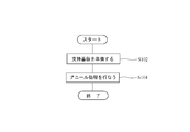
- FIG. 2 is a flow chart showing the method for producing a crystal of the present embodiment.
- a crystal having a surface in which SrTiO 3 is exposed on the surface is prepared as an oxide crystal (S102).
- S102 oxide crystal
- This surface is made to be the (210) plane of SrTiO 3 , and necessarily, the surface extends in the direction including the crystal axis of the [001] axis.
- annealing is performed (S104). Details of this annealing process will be described later.
- a concavo-convex structure constituted by planes of at least three types of orientations extending along the crystal axis [001] axis direction is formed on the surface of the crystal.
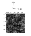
- FIG. 3 shows an AFM image of the surface of a commercially available SrTiO 3 (210) single crystal substrate.
- an AFM image is an image in which each pixel has a half tone originally, in this paper surface, the half tone is expressed by the density of fine black and white pixels.
- the surface is flat at the sub-nm level, and ordered structures such as steps and terraces can not be seen.
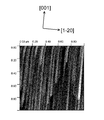
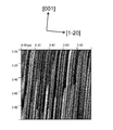
- FIG. 4 shows an AFM image of the surface 10 L of the crystal 1 prepared by annealing the low temperature sample of the embodiment, that is, the commercially available SrTiO 3 (210) single crystal substrate.
- the halftone is represented by the density of fine black and white pixels on the paper, as in FIG.
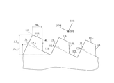
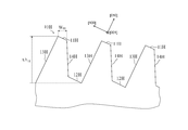
- FIG. 5: is a schematic diagram which shows the surface shape at the time of cut
- an elongated ridge with a width W L of about 40 nm is extended in the [001] axial direction with a length of 1 ⁇ m or more.
- the concavo-convex structure formed in the low temperature sample of the example is a top face 11L which is the top of the concavities and a bottom face which is the bottom. It has been confirmed that it is formed to include two surfaces 12L and a slope face 13L and a slope 14L forming a step between them.
- the top plane 11L and the bottom plane 12L are planes parallel to each other and parallel to the (100) plane of the crystal lattice and directed to the same side. The orientations of such top surface 11L and bottom surface 12L are counted as one type in the present application.
- the graded surface 13L is a plane parallel to the (010) plane of the crystal lattice.
- RHEED reflection high energy electron diffraction
- the RHEED pattern an arrowhead type corresponding to a facet generated by the (100) plane and the (010) plane of the crystal lattice at a position on the diffraction pattern screen different from the peak generated by the specular component of the surface 10L.
- Diffraction patterns i.e. characteristic diffraction patterns with sloping streaks on both sides were observed (not shown).
- a step terrace structure with only two types of surfaces is a terrace with a (010) surface connecting the bottom surface 12L and the virtual surface 12A and a partial step below the slope 13L. It is formed. At this time, the surface corresponding to the slope 14L is not formed.
- the height difference ⁇ h A in that case is, for example, a value about the lattice constant of the unit cell.
- the concavo-convex structure obtained in the low temperature sample of the example has a height difference of about 3 nm which is increased compared to the height difference ⁇ h A caused by the step-like step terrace structure composed of the two types of oriented surfaces. has a surface shape of the unevenness is repeated the difference Delta] h L.
- step difference is drawn as one inclined surface in the schematic diagram of FIG. 5, it was unclear in practice what kind of surface it was.
- the top surface 11L and the bottom surface 12L on both sides of the slope 14L are a pair of surfaces having a difference in height, which are discontinuous in the same direction.
- the slope 14L of FIG. 5 has some surface that increases in height from the bottom surface 12L to the top surface 11L. Therefore, the slope 14L includes at least one type of orientation surface (whether it is a flat surface or a curved surface) which is different from the orientation of the top surface 11L and the bottom surface 12L and the orientation of the slope 13L.
- the slope 14L may be a reverse face parallel to the slope 13L.
- the slope 14L is a surface having a direction different from that of the slope 13L.
- the surface 10L of the low temperature sample of the embodiment includes the concavo-convex structure including at least three types of oriented faces and extending in the direction of the [001] axis. That is, the top surface 11L and the bottom surface 12L facing in the first direction, the second direction slope 13L different from the first direction, and the first direction both have at least three types of directions.
- the slope surface 14L of the third orientation different from the orientation of the third embodiment forms a concavo-convex structure.
- the top surface 11L, the bottom surface 12L, and the slopes 13L and 14L are surfaces extending in the extending direction of the concavo-convex structure, that is, the [001] axis.
- Example of crystal 1 A high temperature sample was produced. Then, in the high temperature sample of the example, it was confirmed from the low temperature sample of the example that the shape changed while maintaining the schematic configuration of the concavo-convex structure of the surface 10L.
- FIG. 6 is an AFM image of the surface 10 H of the example high temperature sample of the crystal 1. It is the same as FIGS. 3 and 4 that the halftone is expressed by the density of fine black and white pixels on the paper.
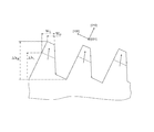
- FIG. 7 is a schematic diagram which shows the surface shape of an Example high temperature sample by the figure similar to FIG. On the surface 10H of the embodiment hot sample, uneven structure elongated convex portion of the width W H of the order of a width of about 20nm extends in the [001] axis direction longer than 1 ⁇ m are formed.
- the height difference of the concavo-convex structure of the surface 10H is measured in the in-plane [1-20] axis direction, it is confirmed that a height difference ⁇ h H of about 6 nm is generated. Note that this height difference is about 12 height differences in terms of unit cells of SrTiO 3 .
- the step edge is formed along the [001] axis direction as in the low temperature sample of the embodiment of the crystal 1.
- the surface 10H in the high temperature sample of the embodiment also had a concavo-convex structure including at least three types of oriented faces and extending in the direction of the [001] axis.
- the surface shape of the high temperature sample of the example had a concavo-convex shape substantially similar to the surface shape of the low temperature sample of the example of FIG. 5. That is, the concavo-convex structure includes two surfaces, ie, a top surface 11L which is the top of the concavities and a bottom surface 12L which is the bottom, and slopes 13L and 14L which form a step between them. Was formed. Also, the orientations of these faces were the same. These configurations were determined by combining the RHEED pattern showing the arrowhead type diffraction pattern corresponding to the facets generated by the (100) plane and the (010) plane, and the AFM image of FIG.
- the effect of the temperature in the annealing process was confirmed.
- the annealing treatment is performed at high temperature, the width of the elongated convex portion is narrowed, and the height difference of the concavo-convex structure is increased.
- the annealing temperature can control the width of the elongated convex portion and the aspect ratio of the height difference of the concavo-convex structure.
- the concavo-convex structure having at least three types of planes extending along the crystal axis is formed to extend generally parallel to the surface of the SrTiO 3 (210) crystal body.
- the first finding is that in the (100) -oriented SrTiO 3 crystal investigated as the first comparative sample, it is reported that Sr or SrO which is an oxide thereof is deposited on the surface by annealing in the air. is there. On the contrary, as far as the inventor knows, such a precipitation phenomenon has not been reported in the (100) oriented LSAT crystal.
- SrTiO 3 and LSAT have different properties under the respective thermal equilibrium conditions determined by the oxygen partial pressure in the air and the annealing temperature. That is, it is thermodynamically stable that SrTiO 3 forms Sr defects in the vicinity of the surface of the crystal body in a thermal equilibrium state and deposits the Sr as it is or as an oxide on the surface.
- LSAT is stable in the state of thermal equilibrium without generating such a defect at the A site.
- the surface energy of the (100) plane is minimum in the Perovskite structure. That is, the precipitated Sr or SrO which is an oxide thereof is likely to be deposited on the (100) plane or the equivalent (010) plane by the thermal energy given at the time of annealing.
- the crystal body 1 which is a SrTiO 3 crystal body of (210) plane orientation, Sr or its oxide with respect to the (100) plane and the (010) plane
- the in-plane [1-20] axis direction left and right direction of the paper surface of FIG. 1A
- the height difference is a step edge (step portion) formed along the [001] axis direction.
- the crystal surface immediately after polishing is randomly controlled whether the terminal surface is SrO or TiO 2, which is different.
- Those components forming the height difference immediately after the polishing also migrate on the surface to find a stable position, also by the thermal energy given by the annealing.
- the deposition on the surface grown anisotropically by Sr or SrO can grow to a height difference as high as several units because it becomes stable in terms of surface energy. If the height difference is too large, the surface energy becomes unstable, and the upper limit of the height difference is determined within that range.
- the reason why the concavo-convex structure is not formed in the comparative example is as follows. First, in the crystal of (100) orientation in the sample of the first comparative example in which the in-plane is four-fold symmetric, such anisotropic growth does not occur, and thus no nanostructure is formed along the crystal axis direction. . In addition, in the LSAT (210) plane orientation crystal sample of the second comparative example, there is no precipitate layer that is an initial trigger, and the (100) plane or (010) plane does not grow anisotropically, so the surface is flattened. It is considered to be a thing. Thus, the inventor believes that adopting so-called asymmetrical off-types such as (210) plane orientation is greatly useful for the development of a novel uneven structure.
- the shape of the surface 10 depends on the final temperature, regardless of the initial state, that is, the as-polished crystal or the crystal that has undergone some kind of annealing. is there. And like the embodiment low temperature sample and the embodiment high temperature sample, it is possible to adjust the width and height difference of the elongated convex portion in the concavo-convex structure by the difference of the annealing temperature.
- FIG. 8 is a schematic view showing how the width of the elongated convex portion and the height difference are controlled by the annealing temperature. The shape that is in thermal equilibrium with the surface 10 is dependent on the annealing temperature.
- the width and height difference of the elongated convex portion of the concavo-convex structure are adjusted. As shown in FIG. 8, when the annealing temperature is high, the height difference of the concavo-convex structure becomes high, and the width of the elongated convex portion becomes narrow. At this time, the period of the unevenness does not change in both the example low temperature sample and the example high temperature sample.
- the concavo-convex structure In order to characterize it as a surface shape separate from the conventional step-terrace structure, another example is different from the above-described example in which the concavo-convex structure observed in the example low temperature sample and the example high temperature sample is focused on the direction of the surface described above. It can also be defined by expression.
- the height of the surface is another aspect that characterizes this relief structure. That is, in the characteristic concavo-convex structure of the present embodiment, the top surface 11L and 11H (hereinafter collectively referred to as "top surface 11" as the same direction of the surfaces of at least three types of directions). And bottom surfaces 12L and 12H (the same, “bottom surface 12”).
- the bottom surface 12 is located between the series of the top surface 11, and the bottom surface 12 is not coplanar with any of the top surfaces 11 on both sides sandwiching it, and the height is low. It has become. Also by such expression, it is possible to define the concavo-convex structure of the present embodiment. Further, in the schematic views of FIGS. 5 and 7, the state in which the concavo-convex structure is formed in a substantially constant cycle has been described, but the concavo-convex structure in the crystal of this embodiment has a shape of such a constant cycle. Is not limited.
- First Embodiment Modified Example The present embodiment can be variously modified. For example, similar crystals can be provided using materials other than strontium titanate described above.
- the examination results of the first embodiment described above apply based on the examination of the extent to which a specific condition is searched.
- Sr-based material a cubic perovskite material (referred to as "Sr-based material") containing Sr (strontium) as an A atom.
- Typical Sr-based materials include materials having the composition formulas of SrFeO 3 , SrVO 3 , SrMnO 3 , and SrCoO 3 .
- SrCrO 3 is not included here. This is because it is difficult to take the state of Cr 4 + .
- what is cubic in SrMnO 3 is limited to the case of a polycrystal.
- SrMnO 3 also has the same crystalline material as that described in the first embodiment, since polycrystalline crystals are also sufficient to constitute a practical device depending on the grain size. It is possible.
- materials having a composition of ABO 3 other than Sr-based are also selected.
- the selection criteria in this case, like Sr, is that point defects are generated by annealing under appropriate conditions such as in the atmosphere.
- Such a material is typically a cubic perovskite material (referred to as a "Ti-based material") containing Ti (titanium) as an A atom.
- the Ti-based material includes a substance having a composition formula of CaTiO 3 , BaTiO 3 , and PbTiO 3 .
- Another typical material is cubic perovskite material (referred to as "K-based material") containing K (potassium) as an A atom.
- the K-based materials include the respective substances of the composition formulas of KNbO 3 and KTaO 3 . In the K-based material, precipitation due to the composition of K 3 O occurs.
- the crystalline body 1 according to the first embodiment described above can be used as various devices utilizing a configuration unique to quantum phenomena generated by the crystalline body 1 itself.
- the crystalline body of the first embodiment described above can use the crystalline body as a substrate. That is, the surface shape and the unique crystal structure associated with the concavo-convex structure of the crystal body 1 of the first embodiment can also be used to exhibit the quantum size effect in the additional object formed thereon .
- the additional object for example, is formed only at the top of the elongated convex portion, is formed along the uneven structure, or is uneven It can be formed to fill the recess and planarize.
- a concavo-convex structure capable of utilizing both anisotropy due to crystal axes and anisotropy due to shape is produced. Ru.
- the concavo-convex structure of the crystal body in the present embodiment is formed along the crystal axis.
- the present invention can be used as a crystal, a substrate, and a method of manufacturing the same, which have a concavo-convex structure that imparts a new function or high performance to a device.
Landscapes
- Chemical & Material Sciences (AREA)
- Engineering & Computer Science (AREA)
- Materials Engineering (AREA)
- Crystallography & Structural Chemistry (AREA)
- Physics & Mathematics (AREA)
- Metallurgy (AREA)
- Organic Chemistry (AREA)
- Thermal Sciences (AREA)
- Nanotechnology (AREA)
- Inorganic Chemistry (AREA)
- Composite Materials (AREA)
- Condensed Matter Physics & Semiconductors (AREA)
- General Physics & Mathematics (AREA)
- Crystals, And After-Treatments Of Crystals (AREA)
Abstract
Description
本実施形態として、立方晶ペロフスカイト構造をとるチタン酸ストロンチウム(SrTiO3)の(210)面方位の単結晶板の表面に、凹凸構造を形成する結晶体について説明する。作製される結晶体を以下、結晶体1という。
まず、図1を参照して、本実施形態の結晶体1において採用される立方晶ペロフスカイト構造であるSrTiO3(210)面方位の単結晶における単位胞について説明する。図1は、立方晶ペロフスカイト構造の(210)面方位の酸化物結晶体の単位胞を示す概略断面図である。例えば、結晶体1に用いるSrTiO3は、立方晶ペロフスカイト構造をとる。この立方晶ペロフスカイト構造は、結晶体1が他の物質である場合の結晶構造でもあるため、一般性を失わない表現によって説明する。
d(210)=a・sinθ 式1
から求められる。このd(210)の値は、結晶体1がSrTiO3であれば、aに約0.3905nm、θに約26.56度を代入することにより、0.1746nmと求められる。また、立方晶のユニットセルが(100)面から26.56度傾いたという見方をすると、面直方向の間隔は、3d(210)である0.5238nmとなる。図1(b)には、d(210)および3d(210)によって示されている間隔を例示している。さらに、面内原子位置における周期性まで考慮した面直方向の長さは5d(210)である0.873nmとなる。
非特許文献1に関連して上述したように、従来、酸化物表面では大気中での1000℃前後でのアニール処理と酸によるウエットエッチング工程によりミスカット角によるステップ・テラス構造が形成される。そこで、アニール処理により結晶体の表面がどのように変化するかを、二つのサンプルを対象に観察した。具体的には、第1比較例サンプルとして、結晶体1と同じSrTiO3を材質とし、図1に示したものとは面方位が異なり(100)面方位である結晶体を観察対象とした。もう一つの第2比較例サンプルとして、結晶体1とは物質が異なり(LaAlO3)0.3-(SrAl0.5Ta0.5O3)0.7(以下「LSAT」と表記する)であるものの、結晶体1と同じく(210)面方位である結晶体を観察対象とした。
第1比較例サンプルのSrTiO3の(100)面方位の結晶体においては、大気雰囲気中、結晶体の到達温度1180~1200℃、12時間アニール、という条件によって、従来と同様のステップ・テラス構造が形成されたことをAFM(原子間力顕微鏡)により確認した。形成されたステップによる高低差はSrTiO3の単位胞に相当する約0.4nmであり、ステップエッジが結晶体の表面において延びる方向と、その結晶体の表面において結晶軸となる方向とは、約30度の角度をなしていた。このように、第1比較例サンプルにおいては、ステップエッジと結晶軸の方向とは一致していなかった。また、第1比較例サンプルにおいて形成されたステップ・テラス構造は、ステップ部の面の向きと、テラス部の面の向きが各1種類の系2種の向きの面から構成されており、その形状は、階段状またはのこぎり歯状の形状であった。さらに、上述のステップエッジが結晶体表面において延びる方向は、(100)面方位を目標に作製された別ロットのSrTiO3の(100)面方位の結晶体では、20度となったことを別途確認している。つまり、第1比較例サンプルと同様の条件のSrTiO3の(100)面方位の結晶体ではステップエッジの方向は制御することができなかった。
第2比較例サンプルのLSATの(210)面方位の結晶体においては、大気雰囲気中、結晶体の到達温度1100℃、12時間アニール、という条件によって従来のステップ・テラス構造が形成されたことをAFMにより確認した。形成されたステップによる高低差は、LSATの単位胞あるいはその2倍に相当する約0.5~1nmであり、ステップエッジが結晶体表面において延びる方向と、その結晶体表面において結晶軸となる方向とは、約40度の角度をなしていた。第1比較例サンプルにおいは、ステップエッジと結晶軸の方向とは一致していなかった。さらに、第2比較例サンプルにおいて形成されたステップ・テラス構造は、ステップ部の面の向きと、テラス部の面の向きが各1種類の計2種の向きの面から構成されており、その形状は、階段状またはのこぎり歯状の形状であった。さらに、上述のステップエッジか結晶体表面において延びる方向は、同一の目標切り出し角によって作製された別ロットのLSATの(210)面方位の結晶体では、10度となったことを別途確認している。つまり、第2比較例サンプルと同様の条件のLSATの(210)面方位の結晶体においてはステップエッジの方向は制御できなかった。
以上の比較例は、ステップ・テラス構造を形成するために必要となるアニール温度が結晶体の物質、結晶体の切り出された面方位によって異なることを示している。そこで、本実施形態の実施例としてSrTiO3(210)面方位の結晶体を採用し、アニール温度を1100℃および1180℃と設定して実施例のための二つのサンプルを作製した。1100℃で12時間アニールを行って作製したSrTiO3(210)の結晶体1のサンプルを、以下「実施例低温サンプル」という。もう一つのサンプルは、一旦製造した結晶体1の実施例低温サンプルに追加のアニール処理を施したサンプルである。このサンプルを、「実施例高温サンプル」という。
上述した比較例および実施例の実験結果に基づいて、結晶体1の表面10Lおよび10H(以下、集合的に「表面10」と記す)において凹凸構造が形成されるメカニズムについて説明する。まず、第1比較例サンプルと第2比較例サンプルの双方におけるステップ・テラス構造はいずれも結晶軸方向に沿って形成されてはいない。これらに対し、実施例では、結晶体1のいずれのサンプルにおいても、結晶体1の表面10の結晶軸に沿った凹凸構造が形成されている。このように、結晶体1における凹凸構造が形成されるための条件には、物質と面方位との組み合わせが関係していることがわかる。
次に、実施例に基づいて、アニール処理(図2、S104)において凹凸構造の形状を制御する手法について説明する。実施例にて説明したように、結晶体1の実施例低温サンプルと実施例高温サンプルでは、凹凸構造の細長凸部の幅と高低差とが異なっている。ここで、実際に作製した結晶体1の実施例高温サンプルは、低温(1100℃)にて一度アニール処理された実施例低温サンプルに対して追加の高温(1180℃)でアニール処理を行なったものである。ただし、十分な時間だけ実施したアニール処理では、表面10の形状は最終の温度に依存し、初期状態、つまり研磨したままの結晶体であったか何らかのアニール処理を経た結晶体であったか、には無関係である。そして、実施例低温サンプルと実施例高温サンプルのように、アニール温度の違いによって、凹凸構造における細長凸部の幅や高低差を調整することが可能である。図8は、アニール温度により細長凸部の幅と高低差とが制御される様子を示す模式図である。表面10に対して熱平衡状態となる形状は、アニール温度に依存している。そのため、アニール温度を調整することによって凹凸構造の細長凸部の幅や高低差が調整される。図8に示すように、アニール温度を高温にすると、凹凸構造の高低差が高くなり、細長凸部の幅が狭くなる。このとき、実施例低温サンプルと実施例高温サンプルとの両者において、凹凸の周期は変化していない。したがって、結晶体1の凹凸構造の部分に発現する量子現象を利用したり、または、結晶体1の凹凸構造を利用して他のナノ構造を形成して量子現象を利用する場合には、凹凸構造の高低差や細長凸部の幅を所望の形状になるようにある程度制御することが可能である。
結晶構造に沿って形成されるステップ部の高低差が大きすぎる場合には、アニール後に酸を用いてウエットエッチングを行なうことにより、堆積されたSrあるいはその酸化物であるSrOを除去し、ステップ部の高低差を1単位胞にまで小さくすることも可能である。すなわち、低めのアニール温度でナノ構造を形成してから酸によるウエットエッチングを行う、という工程を数回繰り返すことによっても、所望の高低差に制御することが可能である。
従来のステップ・テラス構造とは別個の表面形状として特徴付けるために、上述した実施例低温サンプルと実施例高温サンプルにおいて観察された凹凸構造を、上述した面の向きに着目するものとは異なる別の表現によって規定することもできる。例えば、面の高さは、この凹凸構造を特徴付ける別の側面(aspect)である。すなわち、本実施形態の特徴的な凹凸構造には、少なくとも3種の向きの面のうちの同一の向きの面として、頂部面11Lおよび11H(以下、集合的に、「頂部面11」と記す)、ならびに、底部面12Lおよび12H(同、「底部面12」)が存在する。そして、頂部面11の連なりの間に底部面12が位置し、底部面12が、それを挟む両側の頂部面11のいずれとも同一平面になく不連続で高さが低くなっているような面となっている。このような表現によっても、本実施形態の凹凸構造を規定することが可能である。また、図5および図7の模式図においては、ほぼ一定の周期に凹凸構造が形成されている状態を説明したが、本実施形態の結晶体における凹凸構造はこのような一定の周期の形状には限定されない。
本実施形態は、種々の変形を行なうことができる。例えば、上述したチタン酸ストロンチウム以外の材料を用いて同様の結晶体を提供することもできる。特に、ペロフスカイト構造として、ABO3の組成を持つ材質では上述した第1実施形態の検討結果が、具体的な条件を探索する程度の検討によって当てはまる。
上述した第1実施形態の結晶体は、その結晶体を基板として用いることができる。つまり、第1実施形態の結晶体1の凹凸構造に伴う表面形状や特有の結晶構造を、その上に形成される付加的な物体に量子論的なサイズ効果を発現させるために用いることもできる。この際、付加的な物体が形成される態様には特段の限定はなく、付加的な物体、例えば、細長凸部の頂部のみに形成されたり、凹凸構造に沿って形成されたり、凹凸構造の凹部をうめて平坦化するように形成されることが可能である。
2 ペロフスカイト型マンガン酸化物薄膜
10L、10H 表面
11L、11H 頂部面
12L、12H 底部面
12A 仮想面
13L、13H、14L、14H 法面
Claims (8)
- 酸化物結晶を露出させ該酸化物結晶の結晶軸を含む方向に延びている表面を備えてなり、
該表面が、該結晶軸に沿って延びる少なくとも3種の向きの面によって構成される凹凸構造を有している
結晶体。 - 前記酸化物結晶がペロフスカイト構造の結晶構造を有しており、
前記結晶軸が該酸化物結晶の[001]軸であり、
前記凹凸構造が該酸化物結晶の(210)面に対し概して平行に広がっている、
請求項1に記載の結晶体。 - 前記酸化物結晶がチタン酸ストロンチウム(SrTiO3)であり、
前記凹凸構造が1100℃以上の到達温度でアニール処理することによって形成されたものである
請求項2に記載の結晶体。 - 前記少なくとも3種の向きの面が、
第1の向きの頂部面と
該第1の向きの底部面と、
前記第1の向きと異なる第2の向きの法面と、
前記第1の向きとも前記第2の向きとも異なる第3の向きの法面と
を有することにより、前記凹凸構造をなしている
請求項1に記載の結晶体。 - 前記凹凸構造が、2種の向きの面からなる階段状のステップ・テラス構造によって生じる高低差に比較して増大された高低差で繰り返す凹凸の表面形状を有している
請求項1乃至請求項3のいずれか1項に記載の結晶体。 - 請求項1乃至請求項4のいずれか1項に記載の結晶体
を備える
結晶基板。 - 表面に凹凸構造を有する結晶体の製造方法であって、
酸化物結晶を露出させ該酸化物結晶の結晶軸を含む方向に延びている表面を有する結晶体を準備する工程と、
前記結晶軸方向に沿って延びる少なくとも3種の向きの面によって構成される凹凸構造を、アニールによって形成する工程と
を含む結晶体の製造方法。 - 前記酸化物結晶が(210)面方位のチタン酸ストロンチウム(SrTiO3)であり、
前記凹凸構造を形成する工程が、1100℃以上の到達温度でアニールする工程である
請求項7に記載の結晶体の製造方法。
Priority Applications (4)
| Application Number | Priority Date | Filing Date | Title |
|---|---|---|---|
| CN201280013341.1A CN103429799B (zh) | 2011-03-14 | 2012-03-02 | 晶体物质、基材,及生产晶体物质的方法 |
| US14/002,587 US8932699B2 (en) | 2011-03-14 | 2012-03-02 | Crystalline substance, substrate, and method for producing crystalline substance |
| JP2013504650A JP5725156B2 (ja) | 2011-03-14 | 2012-03-02 | 結晶体、基板およびその作製方法 |
| DE112012001248.8T DE112012001248T5 (de) | 2011-03-14 | 2012-03-02 | Kristalline Substanz, Substrat und Verfahren zur Herstellung der kristallinen Substanz |
Applications Claiming Priority (2)
| Application Number | Priority Date | Filing Date | Title |
|---|---|---|---|
| JP2011-055007 | 2011-03-14 | ||
| JP2011055007 | 2011-03-14 |
Publications (1)
| Publication Number | Publication Date |
|---|---|
| WO2012124507A1 true WO2012124507A1 (ja) | 2012-09-20 |
Family
ID=46830582
Family Applications (1)
| Application Number | Title | Priority Date | Filing Date |
|---|---|---|---|
| PCT/JP2012/055343 Ceased WO2012124507A1 (ja) | 2011-03-14 | 2012-03-02 | 結晶体、基板およびその作製方法 |
Country Status (5)
| Country | Link |
|---|---|
| US (1) | US8932699B2 (ja) |
| JP (1) | JP5725156B2 (ja) |
| CN (1) | CN103429799B (ja) |
| DE (1) | DE112012001248T5 (ja) |
| WO (1) | WO2012124507A1 (ja) |
Families Citing this family (4)
| Publication number | Priority date | Publication date | Assignee | Title |
|---|---|---|---|---|
| JP5472533B2 (ja) * | 2011-05-19 | 2014-04-16 | 富士電機株式会社 | 熱電変換構造体およびその製造方法 |
| CN103746071B (zh) * | 2014-01-09 | 2018-01-19 | 北京工业大学 | 一种自组装LaAlO3纳米线、制备及应用 |
| US12247317B2 (en) | 2019-09-04 | 2025-03-11 | The Johns Hopkins University | Functional metal oxides and methods of making same |
| US12074235B2 (en) * | 2019-09-11 | 2024-08-27 | Wisconsin Alumni Research Foundation | Seeded solid-phase crystallization of transparent conducting vanadate perovskites |
Citations (4)
| Publication number | Priority date | Publication date | Assignee | Title |
|---|---|---|---|---|
| JPH07267800A (ja) * | 1994-03-25 | 1995-10-17 | Shinkosha:Kk | 単結晶の表面処理方法 |
| JP2000086400A (ja) * | 1998-09-09 | 2000-03-28 | Inst Of Physical & Chemical Res | 酸化物単結晶基板の製造方法、及び電子デバイス |
| JP2000159600A (ja) * | 1998-11-24 | 2000-06-13 | Agency Of Ind Science & Technol | 単位結晶格子長の階段を有する基板及びその作製方法 |
| JP2006069820A (ja) * | 2004-08-31 | 2006-03-16 | Japan Science & Technology Agency | 酸化物結晶の処理方法及び酸化物結晶 |
Family Cites Families (4)
| Publication number | Priority date | Publication date | Assignee | Title |
|---|---|---|---|---|
| US5855668A (en) | 1994-03-25 | 1999-01-05 | Kabushiki Kaisha Shinkosha | Surface treating method of single crystal |
| JP3401558B2 (ja) * | 1999-12-14 | 2003-04-28 | 独立行政法人産業技術総合研究所 | エピタキシャル複合構造体およびこのものを利用した素子 |
| US7906229B2 (en) * | 2007-03-08 | 2011-03-15 | Amit Goyal | Semiconductor-based, large-area, flexible, electronic devices |
| JP2006096649A (ja) * | 2004-08-30 | 2006-04-13 | Tokyo Institute Of Technology | 金属酸化物単結晶基板表面の平坦化方法及び金属酸化物単結晶基板 |
-
2012
- 2012-03-02 WO PCT/JP2012/055343 patent/WO2012124507A1/ja not_active Ceased
- 2012-03-02 DE DE112012001248.8T patent/DE112012001248T5/de not_active Ceased
- 2012-03-02 JP JP2013504650A patent/JP5725156B2/ja not_active Expired - Fee Related
- 2012-03-02 CN CN201280013341.1A patent/CN103429799B/zh not_active Expired - Fee Related
- 2012-03-02 US US14/002,587 patent/US8932699B2/en not_active Expired - Fee Related
Patent Citations (4)
| Publication number | Priority date | Publication date | Assignee | Title |
|---|---|---|---|---|
| JPH07267800A (ja) * | 1994-03-25 | 1995-10-17 | Shinkosha:Kk | 単結晶の表面処理方法 |
| JP2000086400A (ja) * | 1998-09-09 | 2000-03-28 | Inst Of Physical & Chemical Res | 酸化物単結晶基板の製造方法、及び電子デバイス |
| JP2000159600A (ja) * | 1998-11-24 | 2000-06-13 | Agency Of Ind Science & Technol | 単位結晶格子長の階段を有する基板及びその作製方法 |
| JP2006069820A (ja) * | 2004-08-31 | 2006-03-16 | Japan Science & Technology Agency | 酸化物結晶の処理方法及び酸化物結晶 |
Also Published As
| Publication number | Publication date |
|---|---|
| US8932699B2 (en) | 2015-01-13 |
| JPWO2012124507A1 (ja) | 2014-07-17 |
| CN103429799A (zh) | 2013-12-04 |
| CN103429799B (zh) | 2016-04-20 |
| US20130337228A1 (en) | 2013-12-19 |
| DE112012001248T5 (de) | 2014-01-09 |
| JP5725156B2 (ja) | 2015-05-27 |
Similar Documents
| Publication | Publication Date | Title |
|---|---|---|
| US9761785B2 (en) | Stylo-epitaxial piezoelectric and ferroelectric devices and method of manufacturing | |
| JP6498821B1 (ja) | 膜構造体及びその製造方法 | |
| US8866367B2 (en) | Thermally oxidized seed layers for the production of {001} textured electrodes and PZT devices and method of making | |
| JP5156065B2 (ja) | 圧電単結晶素子 | |
| CN103069056B (zh) | 氧化物基材及其制备方法 | |
| US20130093290A1 (en) | Stylo-Epitaxial Piezoelectric and Ferroelectric Devices and Method of Manufacturing | |
| KR20060083985A (ko) | 압전단결정, 압전단결정소자 및 그 제조방법 | |
| WO2022168800A1 (ja) | 積層構造体及びその製造方法 | |
| JP5725156B2 (ja) | 結晶体、基板およびその作製方法 | |
| JP6881790B2 (ja) | 膜構造体及びその製造方法 | |
| JP2021185614A (ja) | 成膜装置 | |
| JP2000208828A (ja) | 圧電体薄膜素子およびその製造方法 | |
| JP4522013B2 (ja) | 単結晶サファイア基板の熱処理方法 | |
| JP5720698B2 (ja) | ペロフスカイト型マンガン酸化物薄膜 | |
| WO2019093471A1 (ja) | 膜構造体及びその製造方法 | |
| KR100797214B1 (ko) | 압전 단결정소자 및 그 제조방법 | |
| JP5725036B2 (ja) | ペロフスカイト型マンガン酸化物薄膜およびその製造方法 | |
| JP3705695B2 (ja) | 層状ペロブスカイト構造の誘電体薄膜の作製方法、層状ペロブスカイト構造の誘電体薄膜及び層状ペロブスカイト構造の誘電体薄膜を有する電子部品 | |
| JP7338082B1 (ja) | 圧電体膜基板の製造方法および圧電体膜基板 | |
| Bachelet et al. | Self-patterned oxide nanostructures grown by post-deposition thermal annealing on stepped surfaces | |
| JP4977640B2 (ja) | 機能性酸化物構造体、及び機能性酸化物構造体の製造方法 | |
| US12320032B2 (en) | Ferroelectric thin film and forming method thereof | |
| JP2010168280A (ja) | 単結晶サファイア基板 | |
| DE112017003384T5 (de) | Piezoelektrischer Film und piezoelektrisches Element mit einem solchen Film | |
| KR20070023609A (ko) | ZnO계 화합물 반도체 결정의 제조방법, 및 ZnO계화합물 반도체기판 |
Legal Events
| Date | Code | Title | Description |
|---|---|---|---|
| WWE | Wipo information: entry into national phase |
Ref document number: 201280013341.1 Country of ref document: CN |
|
| 121 | Ep: the epo has been informed by wipo that ep was designated in this application |
Ref document number: 12757945 Country of ref document: EP Kind code of ref document: A1 |
|
| WWE | Wipo information: entry into national phase |
Ref document number: 14002587 Country of ref document: US |
|
| ENP | Entry into the national phase |
Ref document number: 2013504650 Country of ref document: JP Kind code of ref document: A |
|
| WWE | Wipo information: entry into national phase |
Ref document number: 1120120012488 Country of ref document: DE Ref document number: 112012001248 Country of ref document: DE |
|
| 122 | Ep: pct application non-entry in european phase |
Ref document number: 12757945 Country of ref document: EP Kind code of ref document: A1 |